Embed Size (px)
Citation preview
Electronic Design Process SymposiumApril 2015
Dileep Bhandarkar, Ph. D.
IEEE Life Fellow
Disclaimer
This presentation is based on personal
Experiences over the last 40+ years in industry
and
Is not presented on behalf of
current or past employers.
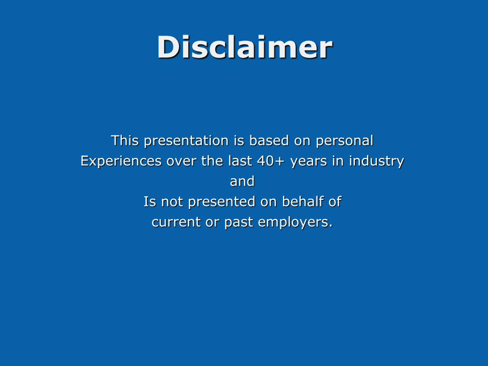
Disruptions Come from Below!
Mainframes
Minicomputers
RISC Systems
Desktop PCs
Notebooks
Smart Phones
Volume
Perf
orm
ance
Bell’s Law: hardware technology, networks, and interfaces allows new, smaller, more specialized computing devices to be introduced to serve a computing need.
The First 50 Yearsafter
Shockley’s Transistor Invention
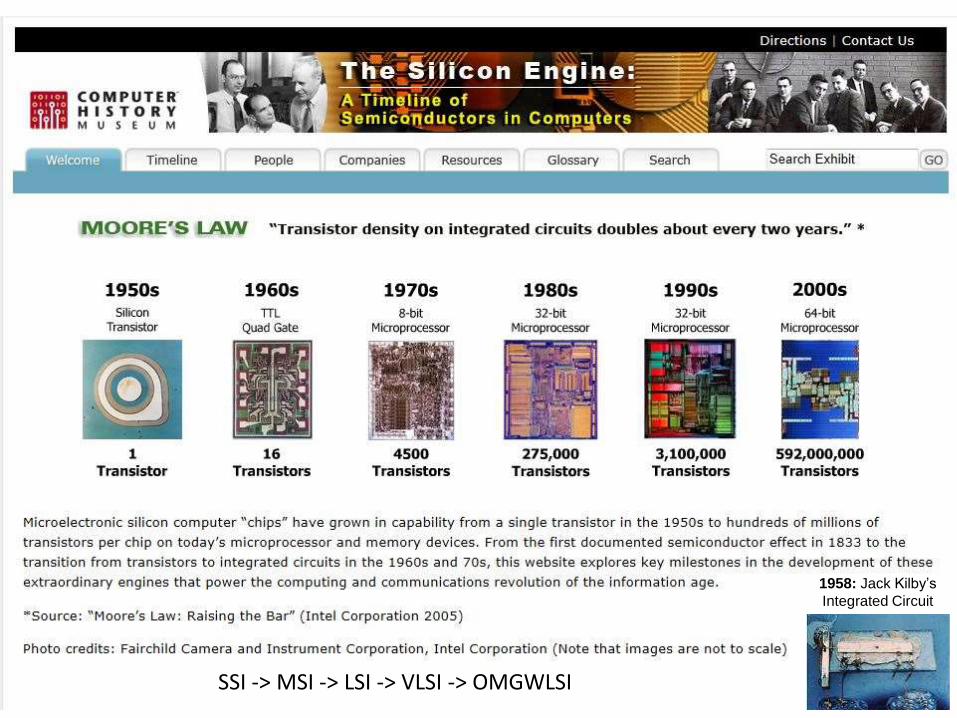
1958: Jack Kilby’s
Integrated Circuit
SSI -> MSI -> LSI -> VLSI -> OMGWLSI

Dennard ScalingDevice or Circuit Parameter Scaling Factor
Device dimension tox, L, W 1/K
Doping concentration Na K
Voltage V 1/K
Current I 1/K
Capacitance eA/t 1/K
Delay time per circuit VC/I 1/K
Power dissipation per circuit VI 1/K2
Power density VI/A 1
Dennard’s 1974 paper summarizes transistor or circuit parameter changes under ideal MOSFET device scaling conditions, where K is the unitless scaling constant.
The benefits of scaling : as transistors get smaller, they can switch faster and use less power. Each new generation of process technology was expected to reduce minimum feature size by
approximately 0.7x (K ~1.4). A 0.7x reduction in linear features size provided roughly a 2x increase in transistor density.
Dennard scaling broke down around 2004 with unscaled interconnect delays and our inability to scale the voltage and the current due to reliability concerns.
But our the ability to etch smaller transistors has continued spawning multicore designs.
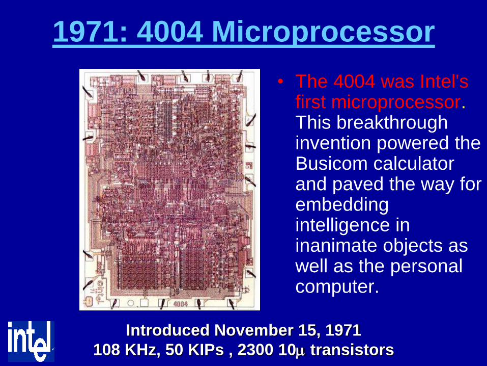
1971: 4004 Microprocessor
• The 4004 was Intel's first microprocessor. This breakthrough invention powered the Busicom calculator and paved the way for embedding intelligence in inanimate objects as well as the personal computer.
Introduced November 15, 1971
108 KHz, 50 KIPs , 2300 10m transistors
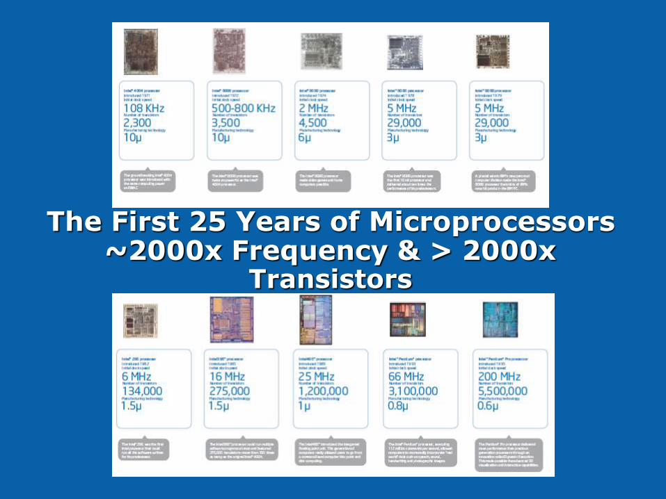
The First 25 Years of Microprocessors~2000x Frequency & > 2000x
Transistors
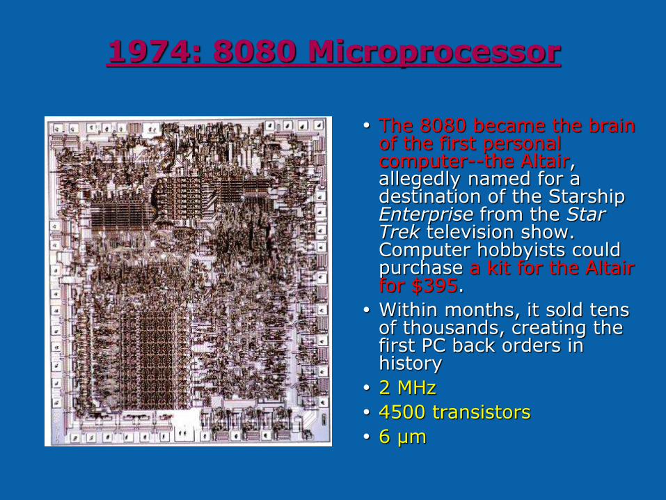
1974: 8080 Microprocessor
The 8080 became the brain of the first personal computer--the Altair, allegedly named for a destination of the Starship Enterprise from the Star Trek television show. Computer hobbyists could purchase a kit for the Altair for $395.
Within months, it sold tens of thousands, creating the first PC back orders in history
2 MHz
4500 transistors
6 µm
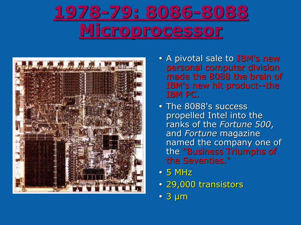
1978-79: 8086-8088 Microprocessor
A pivotal sale to IBM's new personal computer division made the 8088 the brain of IBM's new hit product--the IBM PC.
The 8088's success propelled Intel into the ranks of the Fortune 500, and Fortune magazine named the company one of the "Business Triumphs of the Seventies."
5 MHz
29,000 transistors
3 µm
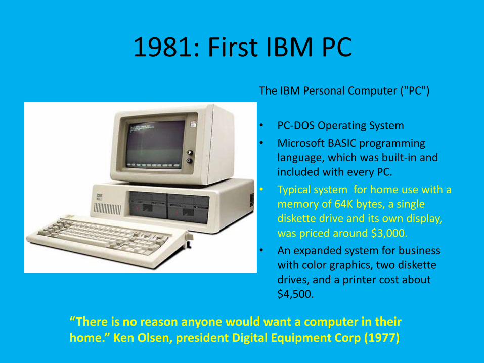
1981: First IBM PC
The IBM Personal Computer ("PC")
• PC-DOS Operating System
• Microsoft BASIC programming language, which was built-in and included with every PC.
• Typical system for home use with a memory of 64K bytes, a single diskette drive and its own display, was priced around $3,000.
• An expanded system for business with color graphics, two diskette drives, and a printer cost about $4,500.
“There is no reason anyone would want a computer in their home.” Ken Olsen, president Digital Equipment Corp (1977)
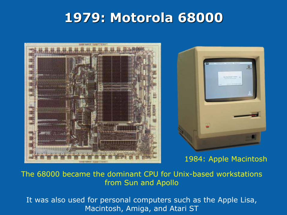
1979: Motorola 68000
The 68000 became the dominant CPU for Unix-based workstations from Sun and Apollo
It was also used for personal computers such as the Apple Lisa, Macintosh, Amiga, and Atari ST
1984: Apple Macintosh
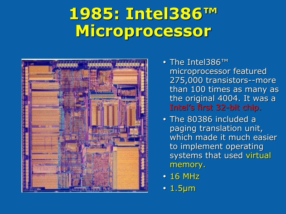
1985: Intel386™ Microprocessor
The Intel386™ microprocessor featured 275,000 transistors--more than 100 times as many as the original 4004. It was a Intel’s first 32-bit chip.
The 80386 included a paging translation unit, which made it much easier to implement operating systems that used virtual memory.
16 MHz
1.5µm
14
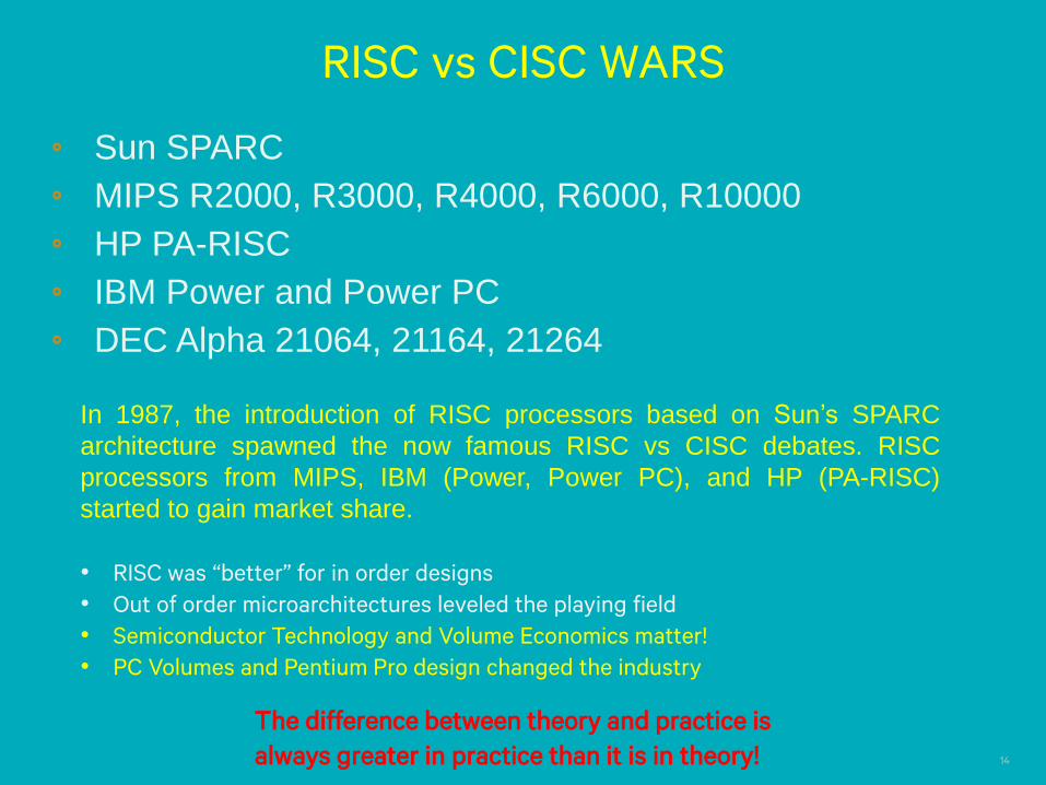
RISC vs CISC WARS
Sun SPARC
MIPS R2000, R3000, R4000, R6000, R10000
HP PA-RISC
IBM Power and Power PC
DEC Alpha 21064, 21164, 21264
In 1987, the introduction of RISC processors based on Sun’s SPARC
architecture spawned the now famous RISC vs CISC debates. RISC
processors from MIPS, IBM (Power, Power PC), and HP (PA-RISC)
started to gain market share.
• RISC was “better” for in order designs
• Out of order microarchitectures leveled the playing field
• Semiconductor Technology and Volume Economics matter!
• PC Volumes and Pentium Pro design changed the industry
The difference between theory and practice is
always greater in practice than it is in theory!
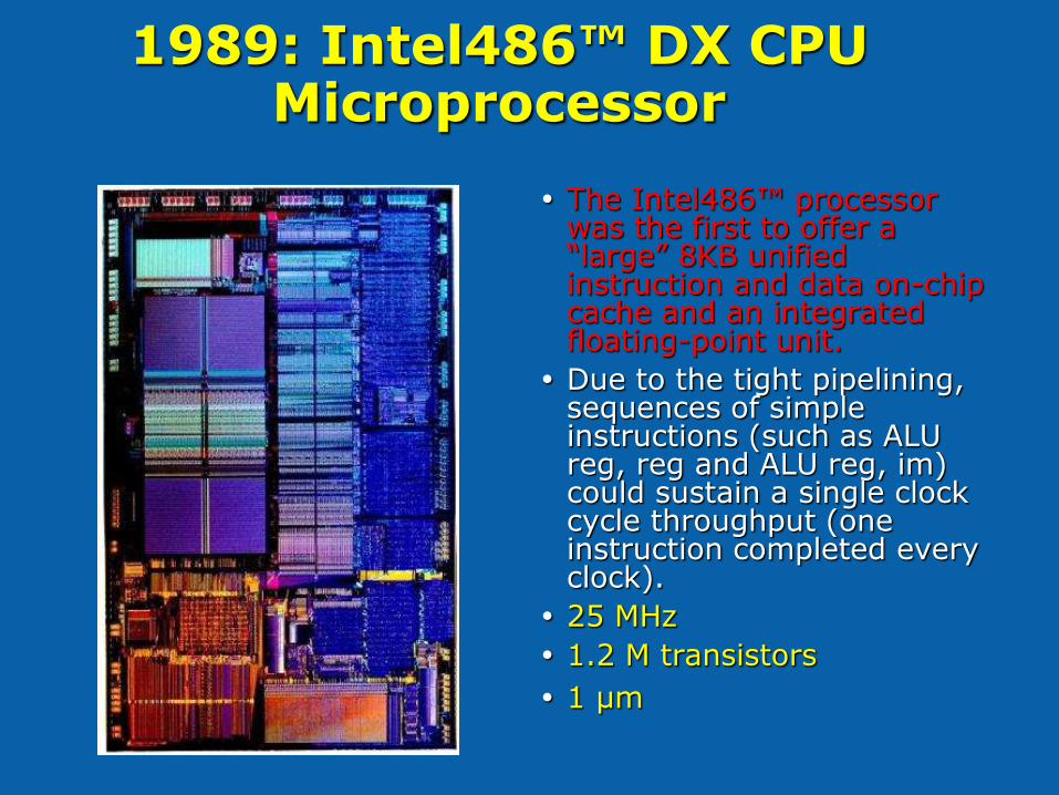
1989: Intel486™ DX CPU Microprocessor
The Intel486™ processor was the first to offer a “large” 8KB unified instruction and data on-chip cache and an integrated floating-point unit.
Due to the tight pipelining, sequences of simple instructions (such as ALU reg, reg and ALU reg, im) could sustain a single clock cycle throughput (one instruction completed every clock).
25 MHz
1.2 M transistors
1 µm
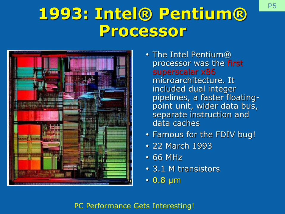
1993: Intel® Pentium® Processor
The Intel Pentium® processor was the first superscalar x86 microarchitecture. It included dual integer pipelines, a faster floating-point unit, wider data bus, separate instruction and data caches
Famous for the FDIV bug!
22 March 1993
66 MHz
3.1 M transistors
0.8 µm
P5
PC Performance Gets Interesting!
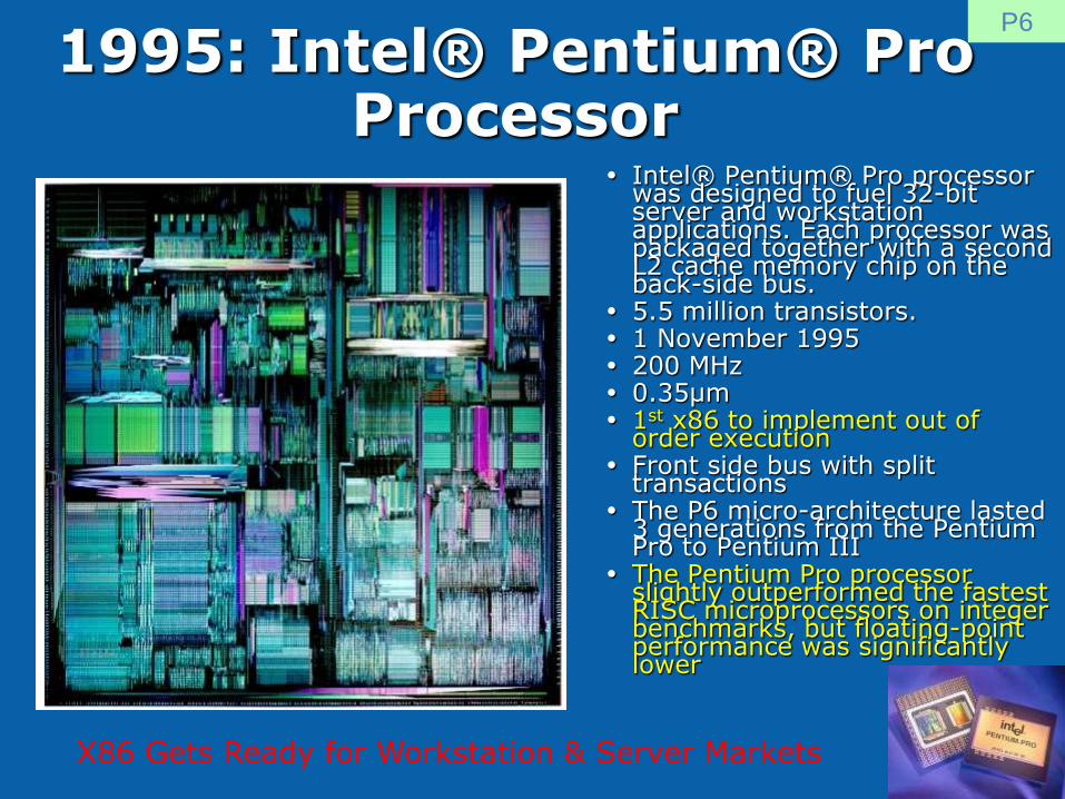
1995: Intel® Pentium® Pro Processor
Intel® Pentium® Pro processor was designed to fuel 32-bit server and workstation applications. Each processor was packaged together with a second L2 cache memory chip on the back-side bus.
5.5 million transistors. 1 November 1995 200 MHz 0.35µm 1st x86 to implement out of
order execution Front side bus with split
transactions The P6 micro-architecture lasted
3 generations from the Pentium Pro to Pentium III
The Pentium Pro processor slightly outperformed the fastest RISC microprocessors on integer benchmarks, but floating-point performance was significantly lower
P6
X86 Gets Ready for Workstation & Server Markets
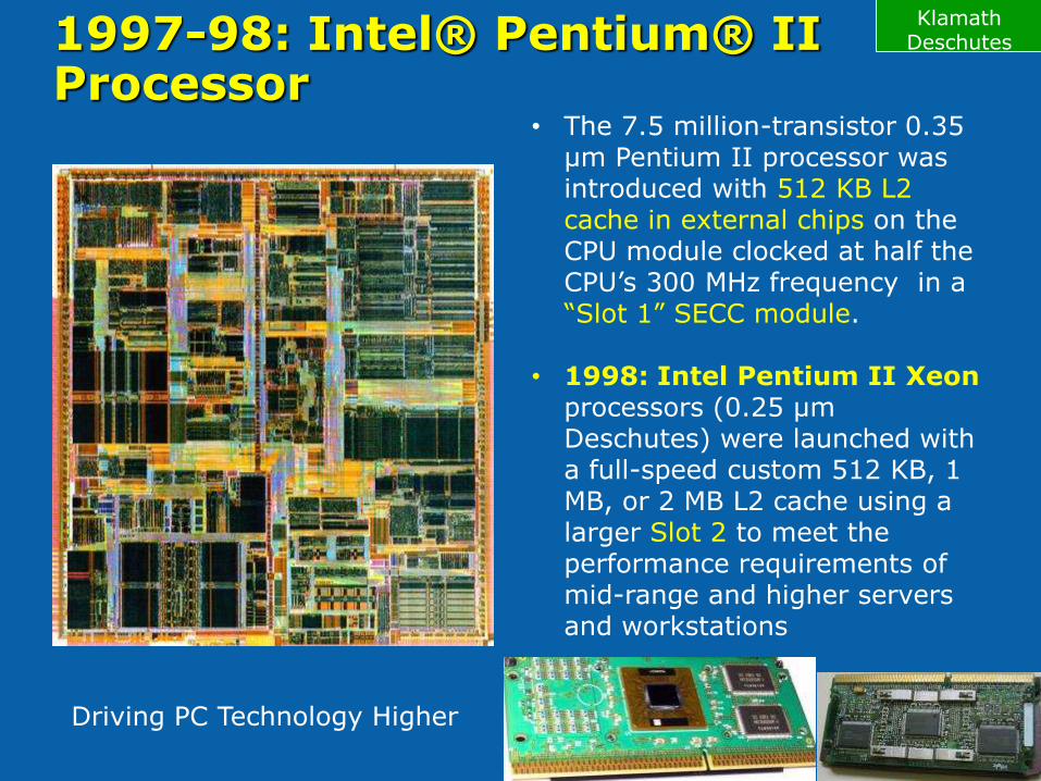
1997-98: Intel® Pentium® II Processor
• The 7.5 million-transistor 0.35 µm Pentium II processor was introduced with 512 KB L2 cache in external chips on the CPU module clocked at half the CPU’s 300 MHz frequency in a “Slot 1” SECC module.
• 1998: Intel Pentium II Xeonprocessors (0.25 µm Deschutes) were launched with a full-speed custom 512 KB, 1 MB, or 2 MB L2 cache using a larger Slot 2 to meet the performance requirements of mid-range and higher servers and workstations
KlamathDeschutes
Driving PC Technology Higher
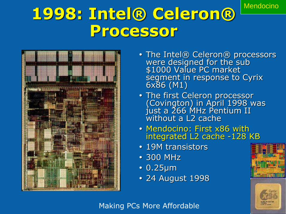
1998: Intel® Celeron® Processor
The Intel® Celeron® processors were designed for the sub $1000 Value PC market segment in response to Cyrix 6x86 (M1)
The first Celeron processor (Covington) in April 1998 was just a 266 MHz Pentium II without a L2 cache
Mendocino: First x86 with integrated L2 cache -128 KB
19M transistors
300 MHz
0.25µm
24 August 1998
Mendocino
Making PCs More Affordable

Clock Frequency Uber Alis
21
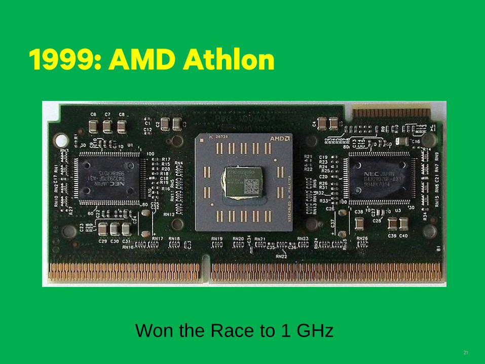
1999: AMD Athlon
Won the Race to 1 GHz
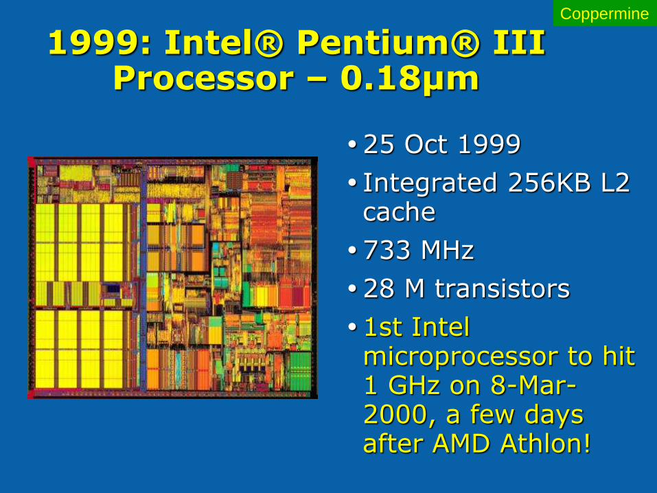
1999: Intel® Pentium® III Processor – 0.18µm
25 Oct 1999
Integrated 256KB L2 cache
733 MHz
28 M transistors
1st Intel microprocessor to hit 1 GHz on 8-Mar-2000, a few days after AMD Athlon!
Coppermine
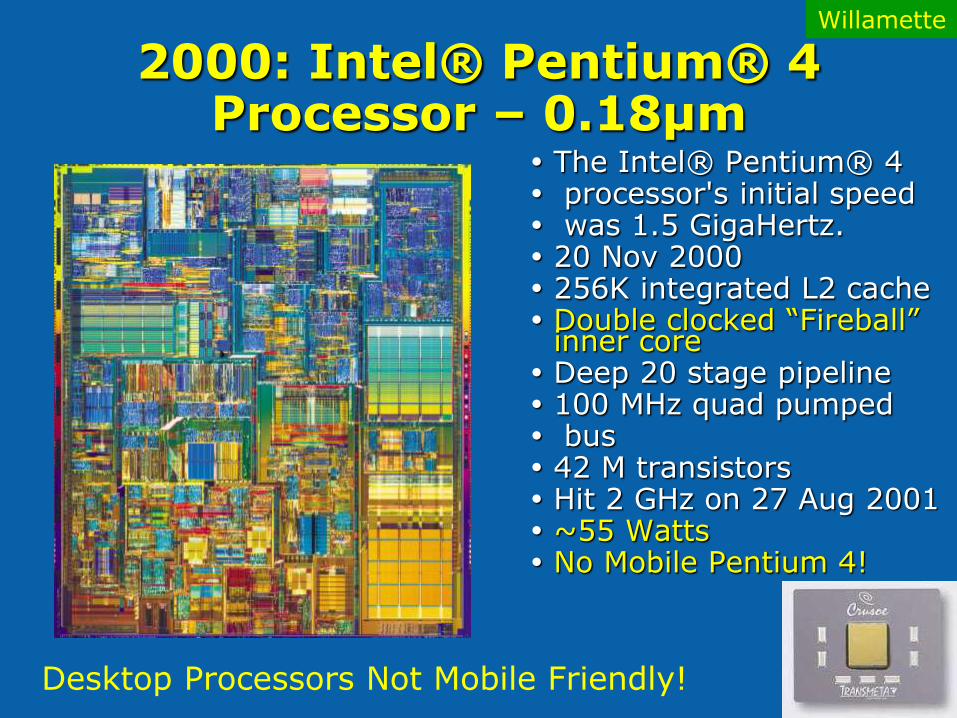
2000: Intel® Pentium® 4 Processor – 0.18µm
The Intel® Pentium® 4 processor's initial speed was 1.5 GigaHertz. 20 Nov 2000 256K integrated L2 cache Double clocked “Fireball”
inner core Deep 20 stage pipeline 100 MHz quad pumped bus 42 M transistors Hit 2 GHz on 27 Aug 2001 ~55 Watts No Mobile Pentium 4!
Willamette
Desktop Processors Not Mobile Friendly!
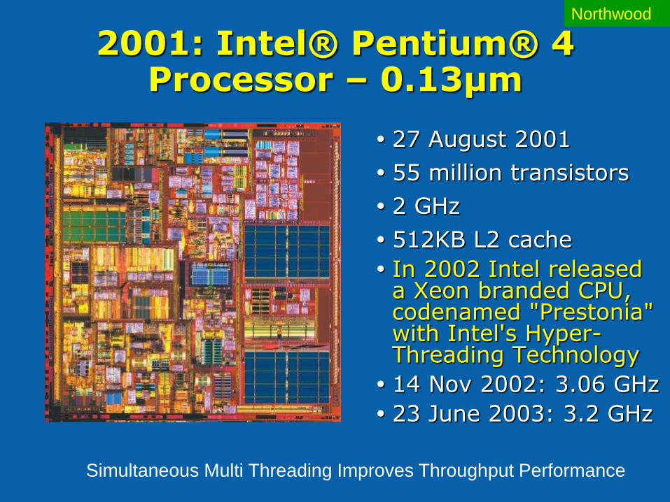
2001: Intel® Pentium® 4 Processor – 0.13µm
27 August 2001
55 million transistors
2 GHz
512KB L2 cache
In 2002 Intel released a Xeon branded CPU, codenamed "Prestonia" with Intel's Hyper-Threading Technology
14 Nov 2002: 3.06 GHz
23 June 2003: 3.2 GHz
Northwood
Simultaneous Multi Threading Improves Throughput Performance
25
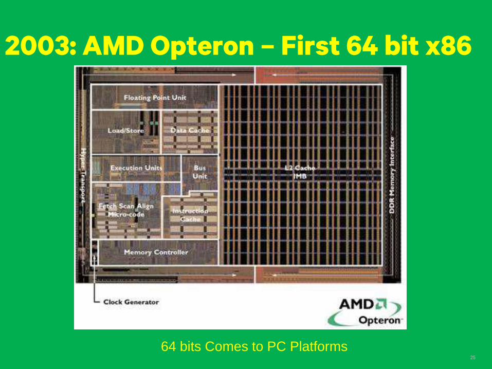
2003: AMD Opteron – First 64 bit x86
64 bits Comes to PC Platforms
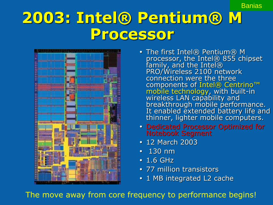
2003: Intel® Pentium® M Processor
The first Intel® Pentium® M processor, the Intel® 855 chipset family, and the Intel® PRO/Wireless 2100 network connection were the three components of Intel® Centrino™ mobile technology, with built-in wireless LAN capability and breakthrough mobile performance. It enabled extended battery life and thinner, lighter mobile computers.
Dedicated Processor Optimized for Notebook Segment
12 March 2003
130 nm
1.6 GHz
77 million transistors
1 MB integrated L2 cache
Banias
The move away from core frequency to performance begins!
THE MULTICORE ERA
NEW DEVICE STRUCTURES
ENERGY EFFICIENCY
Post Dennard Scaling
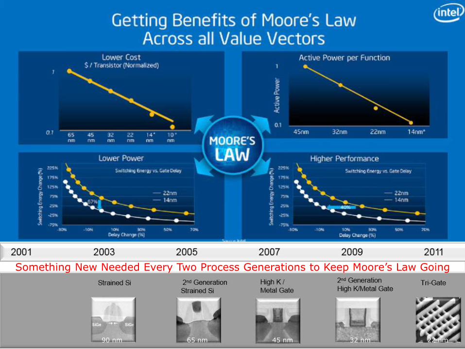
90 nm 65 nm 45 nm 32 nm 22 nm
Something New Needed Every Two Process Generations to Keep Moore’s Law Going
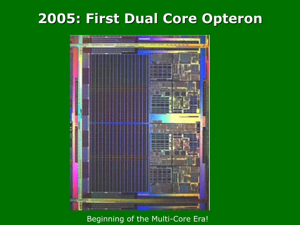
2005: First Dual Core Opteron
Beginning of the Multi-Core Era!
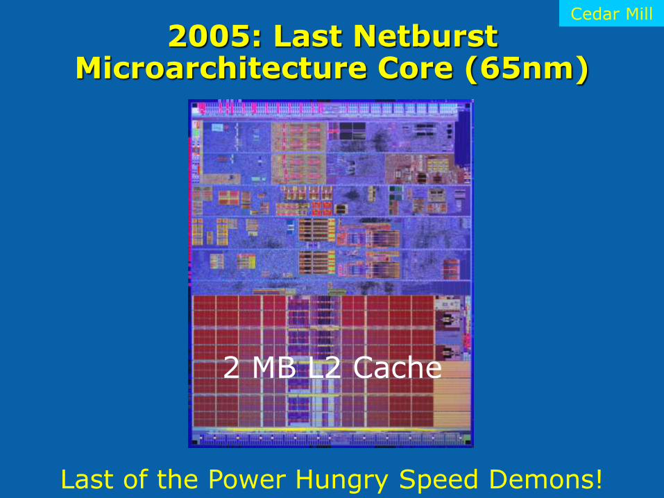
2005: Last NetburstMicroarchitecture Core (65nm)
Cedar Mill
2 MB L2 Cache
Last of the Power Hungry Speed Demons!
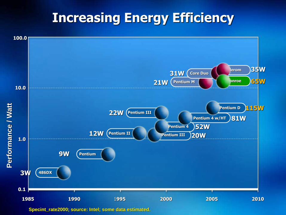
Increasing Energy Efficiency
1985 1990 1995 2000 2005 2010
0.1
1.0
10.0
100.0
3W
Pentium M
Core DuoMerom
486DX
Pentium
Pentium II
Pentium III
Pentium III
Pentium 4
Pentium 4 w/HT
Pentium D
Conroe
9W
12W 20W
52W
81W
115W22W
21W
31W35W
65W
Perf
orm
an
ce /
Watt
Specint_rate2000; source: Intel; some data estimated.
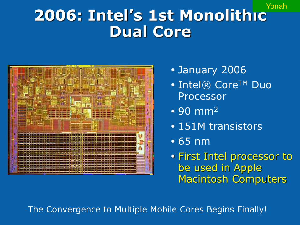
2006: Intel’s 1st Monolithic Dual Core
January 2006
Intel® CoreTM Duo Processor
90 mm2
151M transistors
65 nm
First Intel processor to be used in Apple Macintosh Computers
Yonah
The Convergence to Multiple Mobile Cores Begins Finally!
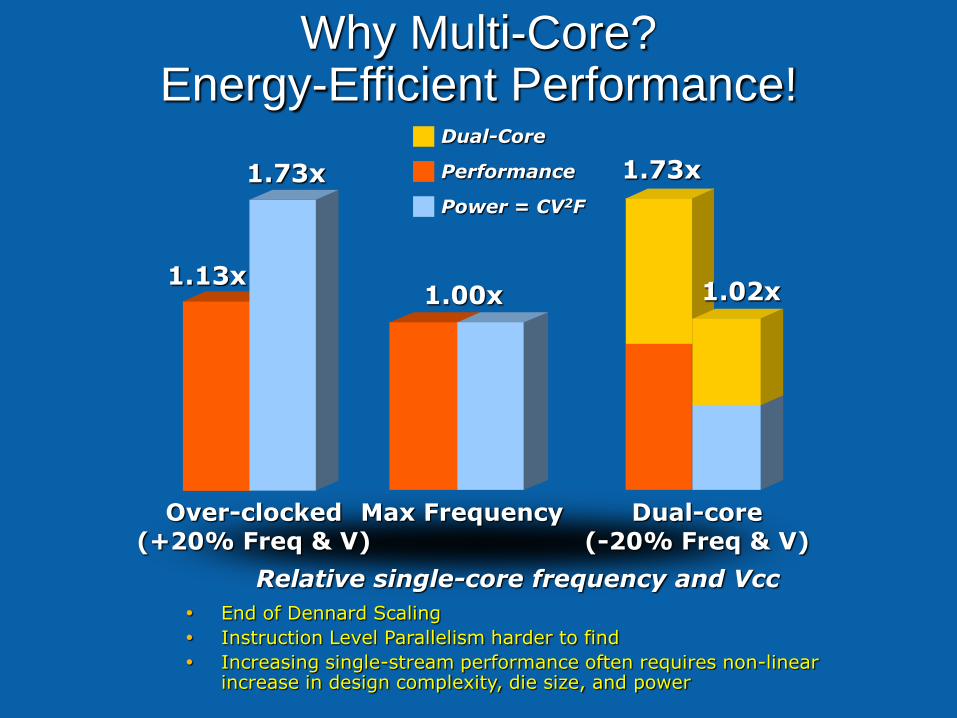
Over-clocked(+20% Freq & V)
1.00x
Relative single-core frequency and Vcc
1.73x
1.13x
Max Frequency
Power = CV2F
Performance
Why Multi-Core?Energy-Efficient Performance!
Dual-core(-20% Freq & V)
1.02x
1.73x
Dual-Core
End of Dennard Scaling
Instruction Level Parallelism harder to find
Increasing single-stream performance often requires non-linear increase in design complexity, die size, and power
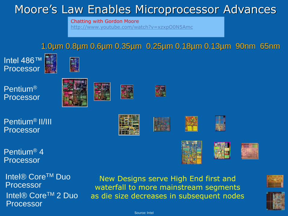
1.0µm 0.8µm 0.6µm 0.35µm 0.25µm 0.18µm 0.13µm 90nm 65nm
Moore’s Law Enables Microprocessor Advances
Source: Intel
Intel 486™ Processor
Pentium®
Processor
Pentium® II/IIIProcessor
Pentium® 4Processor
Intel® CoreTM Duo Processor
Intel® CoreTM 2 Duo Processor
Chatting with Gordon Moore http://www.youtube.com/watch?v=xzxpO0N5Amc
New Designs serve High End first and waterfall to more mainstream segments
as die size decreases in subsequent nodes
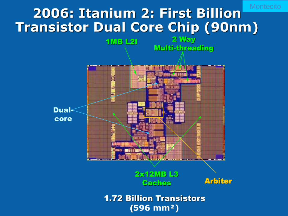
1MB L2I
Dual-
core
2x12MB L3
Caches
1.72 Billion Transistors
(596 mm²)
2 Way
Multi-threading
2006: Itanium 2: First Billion Transistor Dual Core Chip (90nm)
Arbiter
Montecito
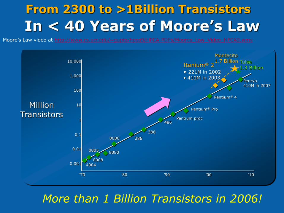
In < 40 Years of Moore’s Law
4004
8008
80808085
8086 286
386
486Pentium proc
Pentium® Pro
Pentium® 4
Itanium® 2• 221M in 2002
• 410M in 2003
0.001
0.01
0.1
1
10
100
1,000
10,000
’70 ’80 ’90 ’00 ’10
MillionTransistors
More than 1 Billion Transistors in 2006!
Montecito1.7 Billion Tulsa
1.3 Billion
Penryn410M in 2007
From 2300 to >1Billion Transistors
Moore’s Law video at http://www.cs.ucr.edu/~gupta/hpca9/HPCA-PDFs/Moores_Law_Video_HPCA9.wmv
4 is Better Than 2!
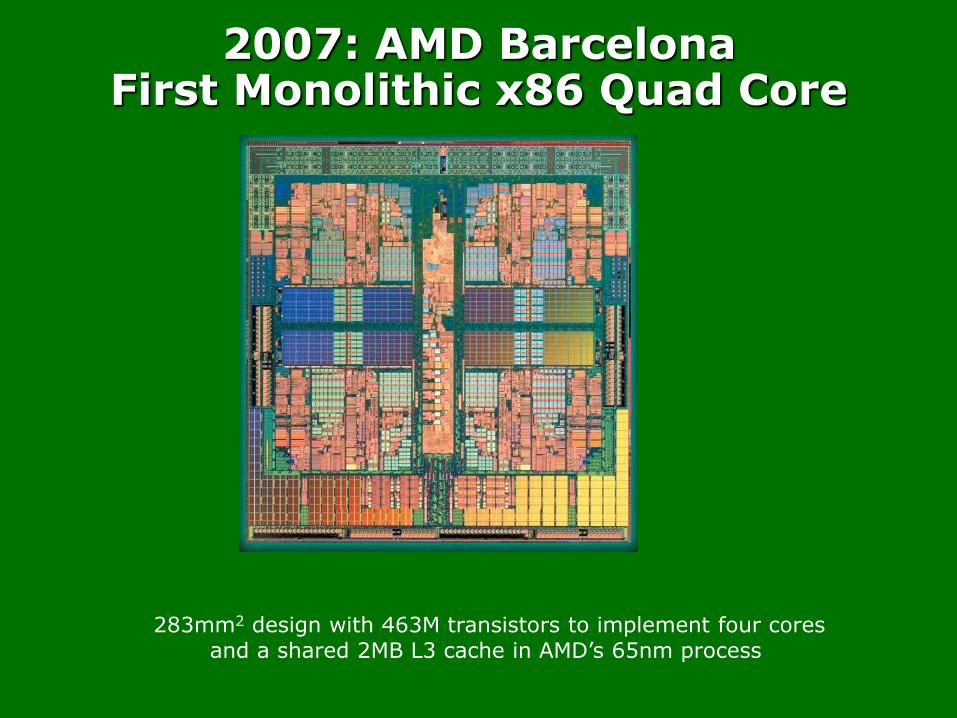
2007: AMD BarcelonaFirst Monolithic x86 Quad Core
283mm2 design with 463M transistors to implement four cores and a shared 2MB L3 cache in AMD’s 65nm process
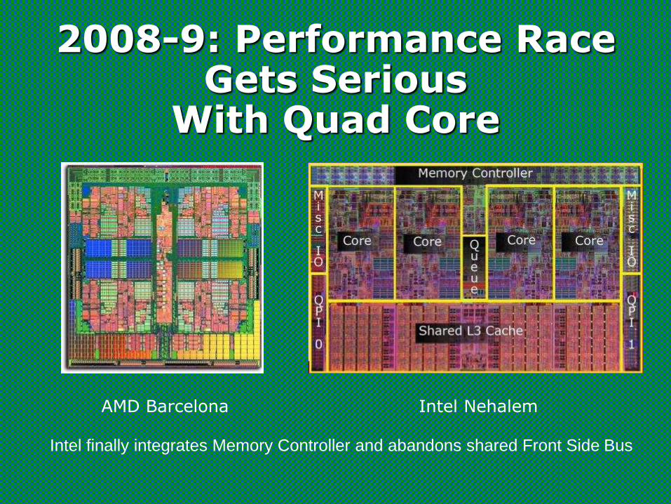
2008-9: Performance Race Gets Serious
With Quad Core
Intel finally integrates Memory Controller and abandons shared Front Side Bus
Intel NehalemAMD Barcelona
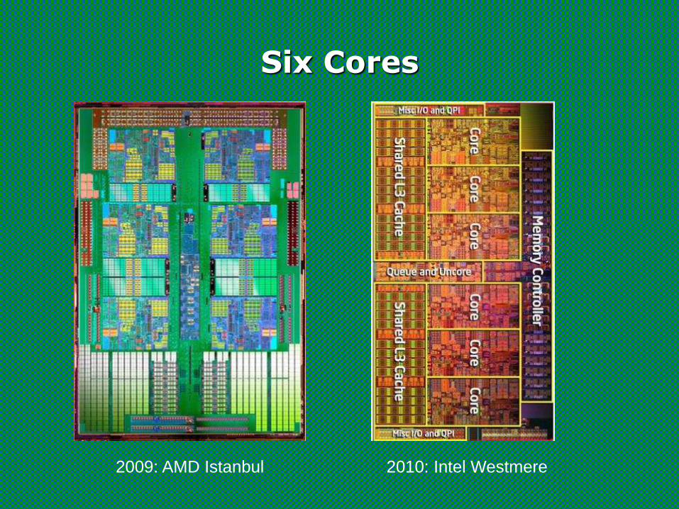
Six Cores
2009: AMD Istanbul 2010: Intel Westmere
SIZE MATTERSSMALL & LIGHT
LOW POWER
Mobile Computing Era
42
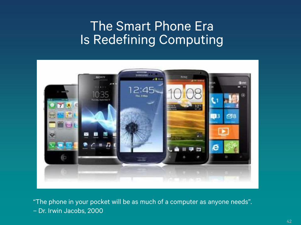
The Smart Phone EraIs Redefining Computing
“The phone in your pocket will be as much of a computer as anyone needs”.
– Dr. Irwin Jacobs, 2000
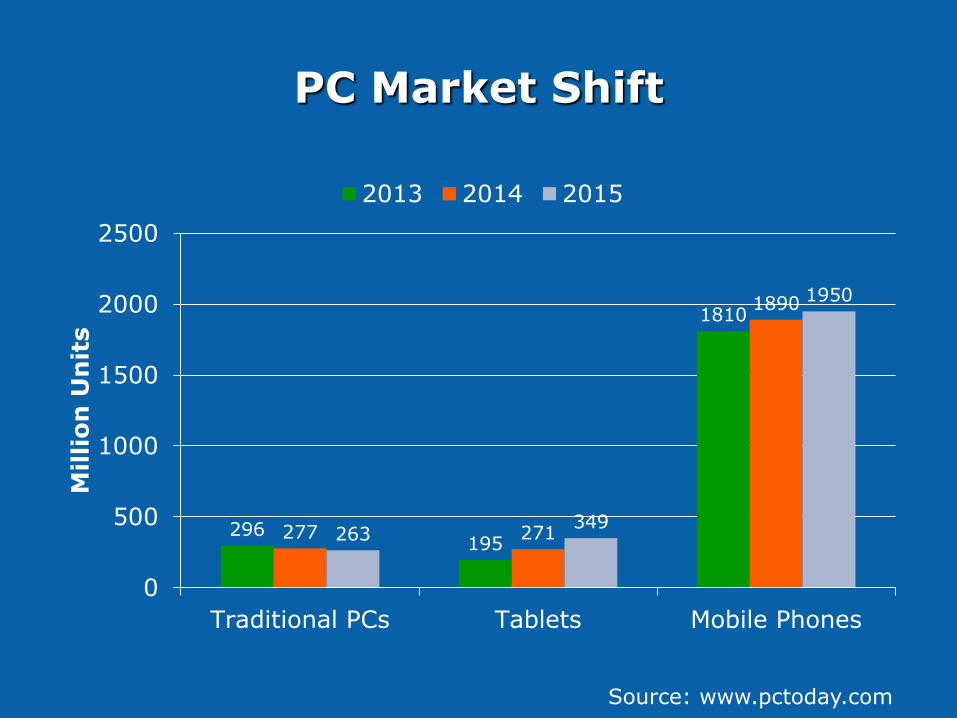
PC Market Shift
296195
1810
277 271
1890
263349
1950
0
500
1000
1500
2000
2500
Traditional PCs Tablets Mobile Phones
Millio
n U
nit
s
2013 2014 2015
Source: www.pctoday.com
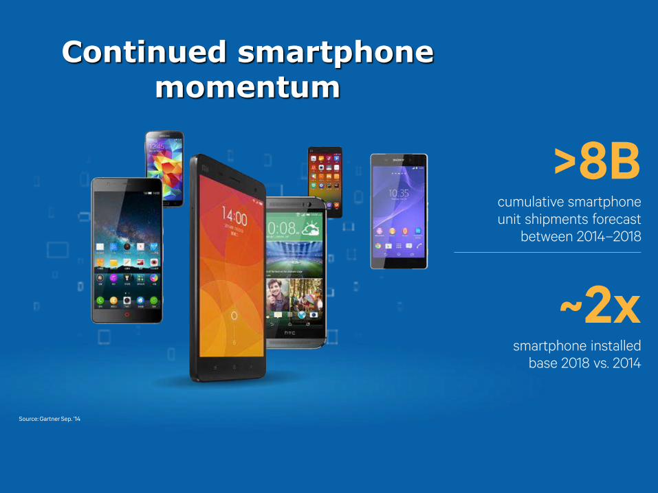
Continued smartphonemomentum
>8Bcumulative smartphone
unit shipments forecast
between 2014–2018
~2xsmartphone installed
base 2018 vs. 2014
Source: Gartner Sep. ’14
2011
2015
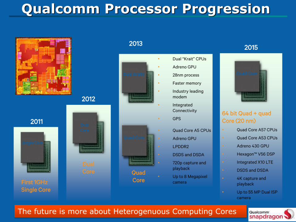
Qualcomm Processor Progression
2012
Dual
Core
Dual
Core
First 1GHz
Single Core
Single Core
2013
Quad Core
Dual Kraits
• Quad Core A5 CPUs
• Adreno GPU
• LPDDR2
• DSDS and DSDA
• 720p capture and
playback
• Up to 8 Megapixel
camera
• Dual “Krait” CPUs
• Adreno GPU
• 28nm process
• Faster memory
• Industry leading
modem
• Integrated
Connectivity
• GPS
Quad Core
64 bit Quad + quad
Core (20 nm)
• Quad Core A57 CPUs
• Quad Core A53 CPUs
• Adreno 430 GPU
• Hexagon™ V56 DSP
• Integrated X10 LTE
• DSDS and DSDA
• 4K capture and
playback
• Up to 55 MP Dual ISP
camera
Quad
Core
The future is more about Heterogenuous Computing Cores
Memory Scheduling & QoS
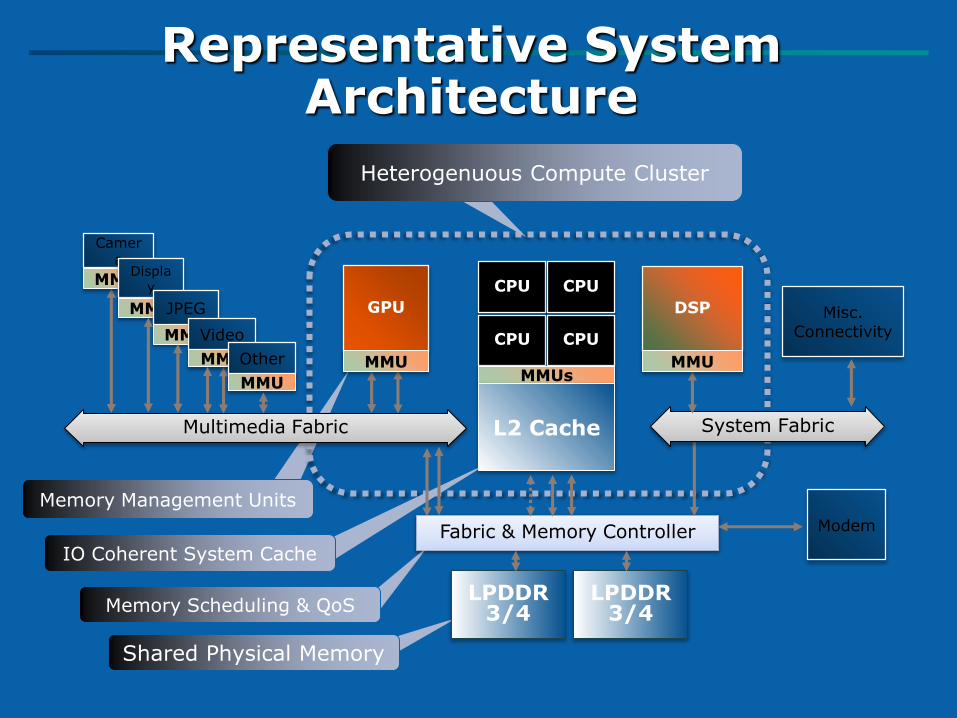
Representative System Architecture
Shared Physical Memory
IO Coherent System Cache
Heterogenuous Compute Cluster
Multimedia Fabric
Fabric & Memory Controller
System Fabric
LPDDR3/4
LPDDR3/4
CPU
GPU
CPU
CPU
CPU
MMUMMUs
L2 Cache
Misc.Connectivity
Modem
Memory Management Units
Camera
MMUDispla
y
MMUJPEG
MMUVideo
MMUOther
MMU
DSP
MMU
47© 2013 Qualcomm Technologies, Inc. All Rights Reserved.
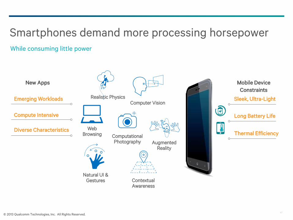
Smartphones demand more processing horsepower
While consuming little power
Thermal Efficiency
Long Battery Life
Sleek, Ultra-Light
Computational Photography
Realistic Physics
Augmented Reality
Contextual Awareness
Natural UI & Gestures
Computer Vision
New Apps
Diverse Characteristics
Emerging Workloads
Compute Intensive
Mobile Device
Constraints
Web Browsing
48© 2013 Qualcomm Technologies, Inc. All Rights Reserved.
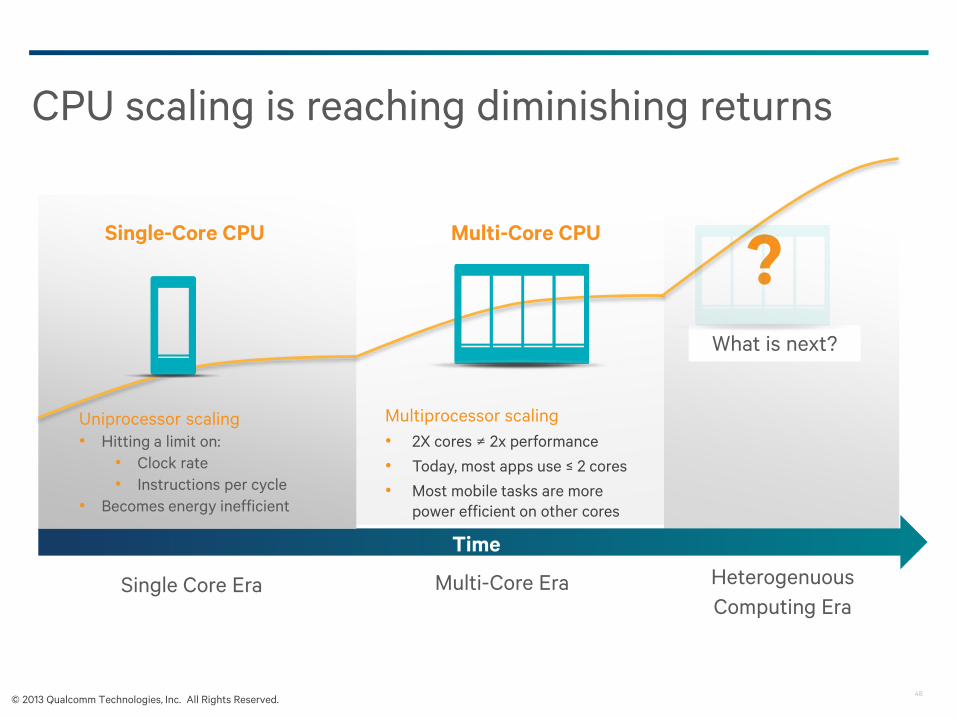
CPU scaling is reaching diminishing returns
Time
Single Core Era
Uniprocessor scaling
• Hitting a limit on:
• Clock rate
• Instructions per cycle
• Becomes energy inefficient
Single-Core CPU
Multi-Core Era
Multiprocessor scaling
• 2X cores ≠ 2x performance
• Today, most apps use ≤ 2 cores
• Most mobile tasks are more
power efficient on other cores
Multi-Core CPU
Multi-Core Era
What is next?
?
Heterogenuous
Computing Era
49© 2013 Qualcomm Technologies, Inc. All Rights Reserved.
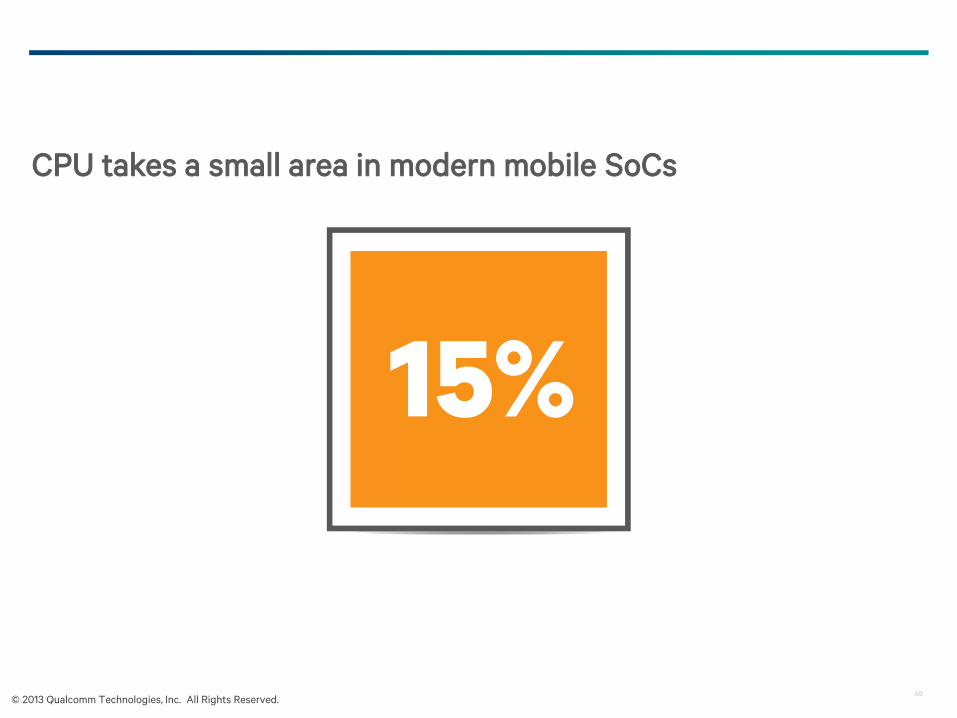
CPU takes a small area in modern mobile SoCs
50© 2013 Qualcomm Technologies, Inc. All Rights Reserved.
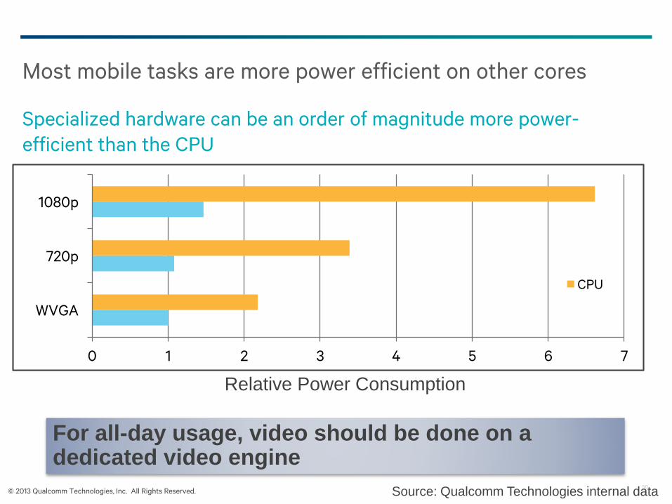
Most mobile tasks are more power efficient on other cores
Specialized hardware can be an order of magnitude more power-
efficient than the CPU
Relative Power Consumption
0 1 2 3 4 5 6 7
WVGA
720p
1080p
CPU
For all-day usage, video should be done on a dedicated video engine
Source: Qualcomm Technologies internal data
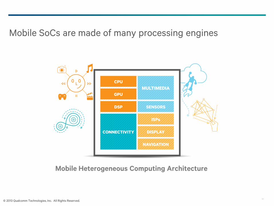
51© 2013 Qualcomm Technologies, Inc. All Rights Reserved.
CPU
GPU
DSP
CONNECTIVITY
ISPs
DISPLAY
NAVIGATION
SENSORS
MULTIMEDIA
Mobile SoCs are made of many processing engines
Mobile Heterogeneous Computing Architecture
52© 2013 Qualcomm Technologies, Inc. All Rights Reserved.
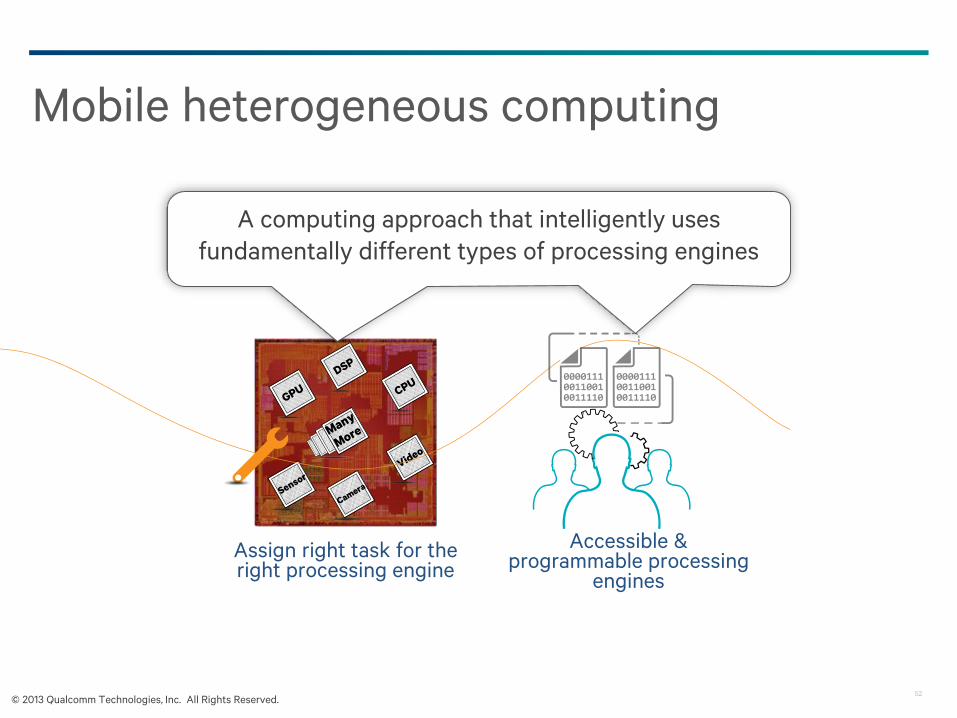
Mobile heterogeneous computing
A computing approach that intelligently uses
fundamentally different types of processing engines
Assign right task for the right processing engine
Accessible & programmable processing
engines
53© 2013 Qualcomm Technologies, Inc. All Rights Reserved.
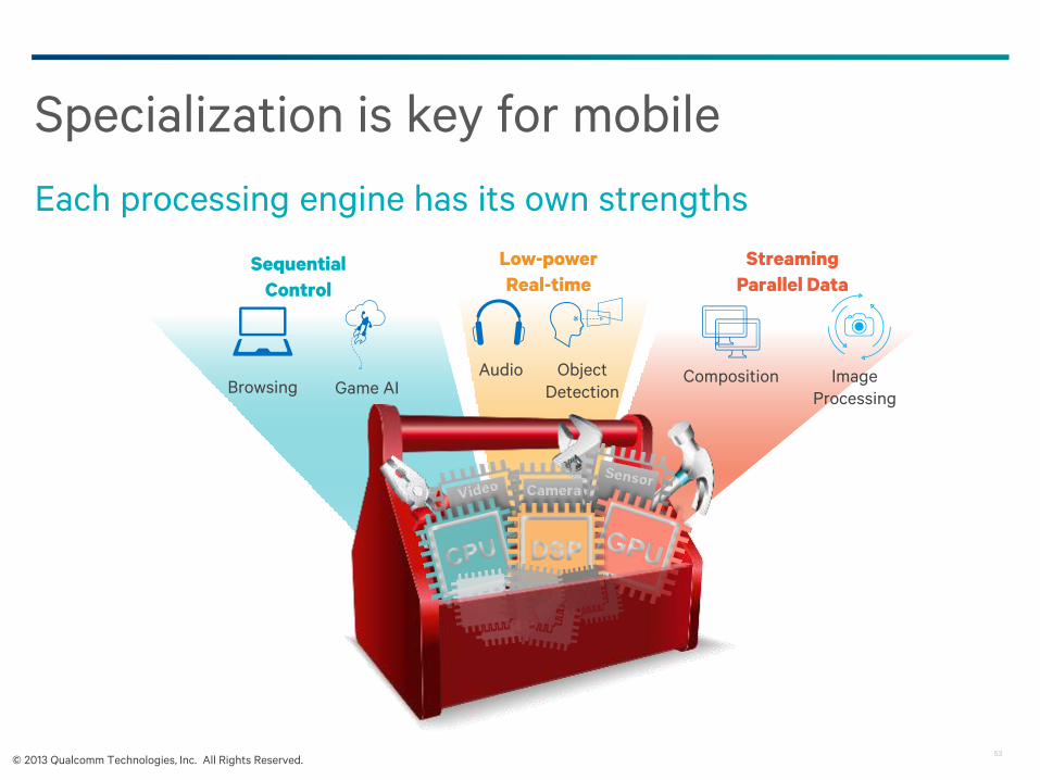
Specialization is key for mobile
Each processing engine has its own strengths
Sequential
Control
Game AIObject
Detection
Audio Image
Processing
Composition
Low-power
Real-time
Streaming
Parallel Data
Browsing
54© 2013 Qualcomm Technologies, Inc. All Rights Reserved.
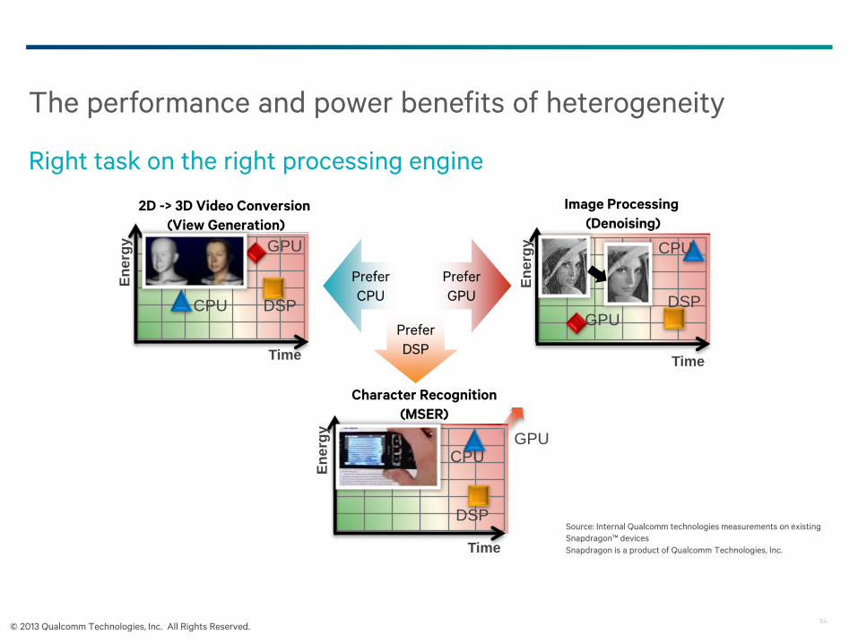
The performance and power benefits of heterogeneity
Right task on the right processing engine
Image Processing
(Denoising)
Character Recognition
(MSER)
2D -> 3D Video Conversion
(View Generation)
En
erg
y
Time
En
erg
y
Time
En
erg
y
Time
GPUDSP
GPU
CPU DSP
CPU
DSP
GPU
CPU
Prefer
DSP
Prefer
CPU
Prefer
GPU
Source: Internal Qualcomm technologies measurements on existing
Snapdragon™ devices
Snapdragon is a product of Qualcomm Technologies, Inc.
55© 2013 Qualcomm Technologies, Inc. All Rights Reserved.
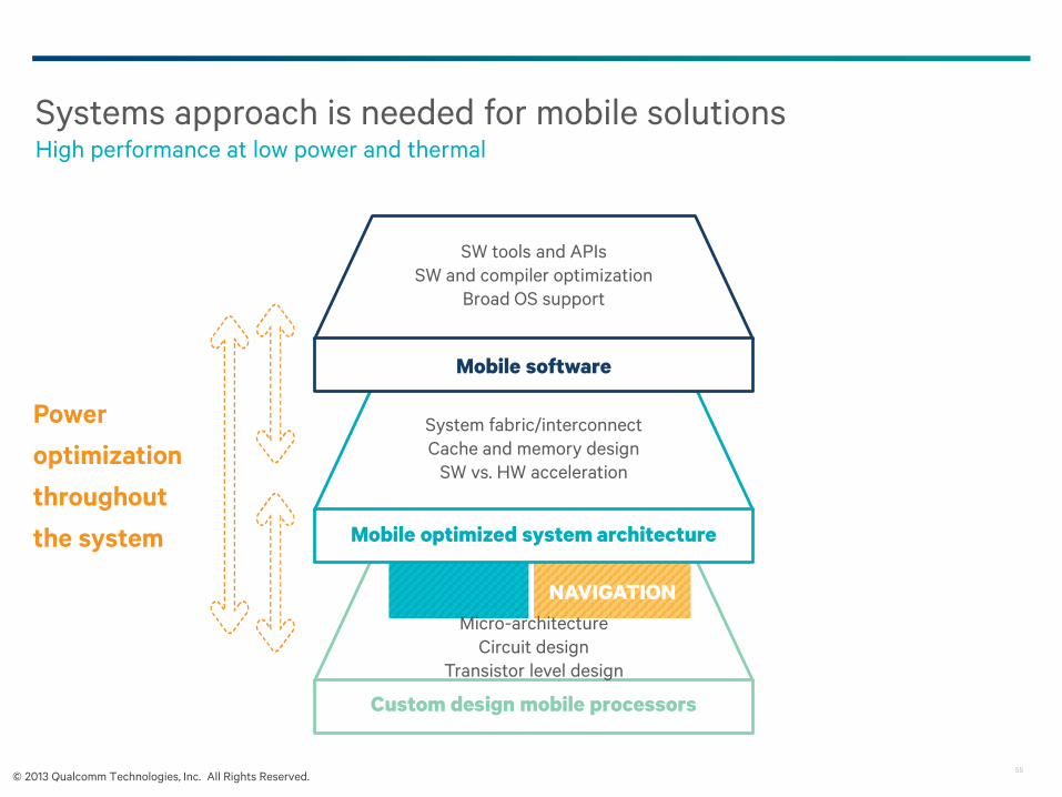
Systems approach is needed for mobile solutionsHigh performance at low power and thermal
CPU
GPU
DSP
CONNECTI
VITY
ISPs
DISPLAY
NAVIGATION
SENSORS
MULTIMEDI
A
Custom design mobile processors
Micro-architecture
Circuit design
Transistor level design
Mobile optimized system architecture
System fabric/interconnect
Cache and memory design
SW vs. HW acceleration
Mobile software
SW tools and APIs
SW and compiler optimization
Broad OS support
Power
optimization
throughout
the system
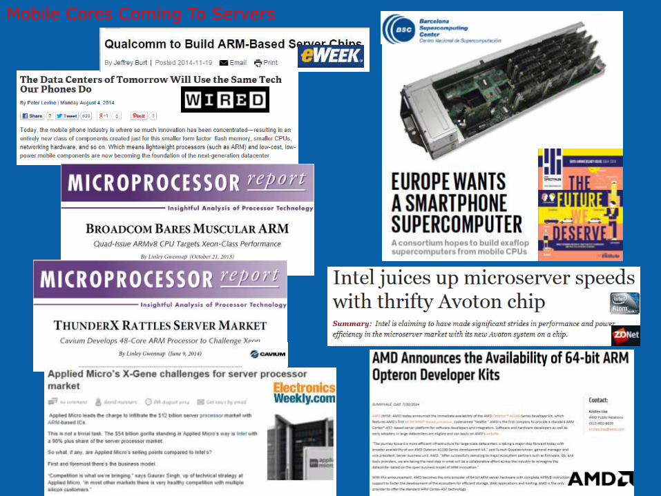
Mobile Cores Coming To Servers
Where is The Industry Today?
14 nm is in production but ramping slower than previous generations
– Future Generations will be even harder!
Costs per wafer increasing
–Capital, more process steps, increased mask costs
– Cost per transistor decreasing
PC sales slowing; Server volume growing
Mobile computing (Smartphones & Tablets) & IoT are driving growth at lower price points
Moore’s Law will slow down beyond 10 nm
– Economics, Physics, Materials, Power
– What is the best use for increased transistor density?
– Heterogenuous Processing Engines Everywhere?
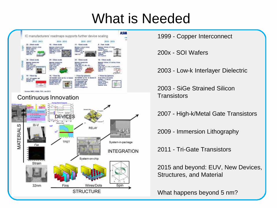
1999 - Copper Interconnect
200x - SOI Wafers
2003 - Low-k Interlayer Dielectric
2003 - SiGe Strained Silicon
Transistors
2007 - High-k/Metal Gate Transistors
2009 - Immersion Lithography
2011 - Tri-Gate Transistors
2015 and beyond: EUV, New Devices,
Structures, and Material
What happens beyond 5 nm?
What is Needed
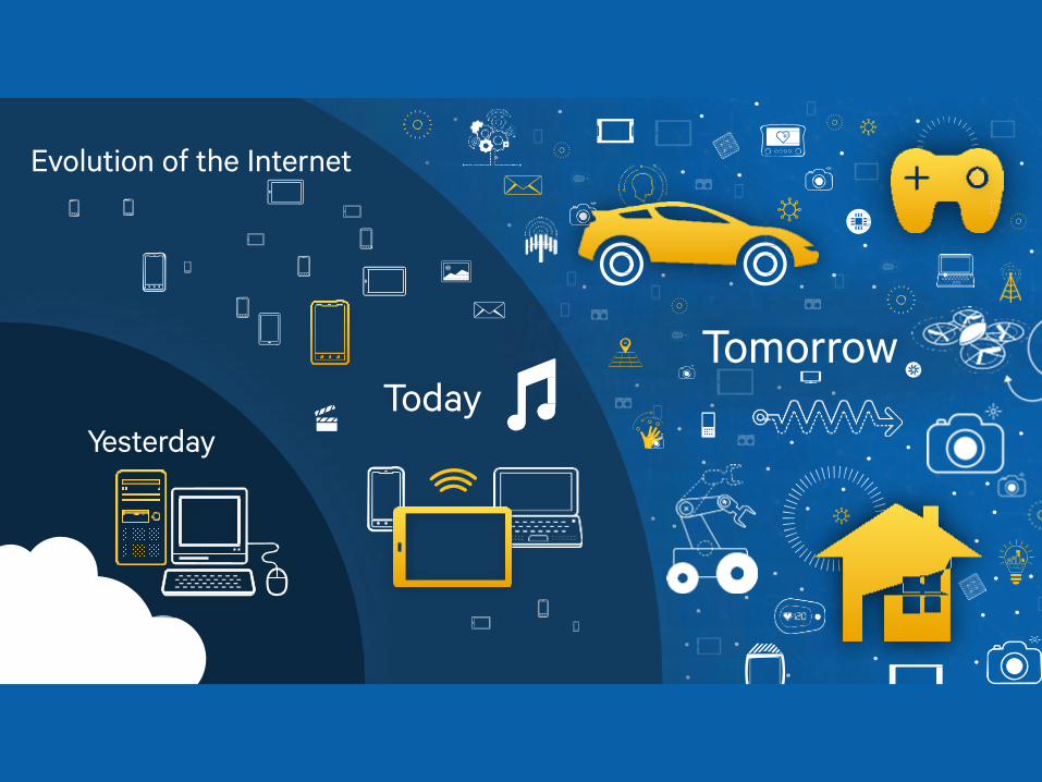
Evolution of the Internet
TodayYesterday
Tomorrow