Embed Size (px)
Citation preview
ARTICLE IN PRESS
Nuclear Instruments and Methods in Physics Research A 520 (2004) 274–276
*Corresp
303-497-304
E-mail a
0168-9002/$
doi:10.1016
Dilute Al–Mn alloys for superconductor device applications
S.T. Ruggieroa,*, A. Williamsa, W.H. Rippardb, A.M. Clarkb, S.W. Deikerb,B.A. Youngc, L.R. Valeb, J.N. Ullomb
aDepartment of Physics, University of Notre Dame, Notre Dame, IN 46556, USAbNational Institute of Standards and Technology, Boulder, CO 80305, USA
c Department of Physics, Santa Clara University, Santa Clara, CA 95053, USA
Abstract
We discuss results on the superconducting and electron-transport properties of Mn-doped Al produced by sputter
deposition. The critical temperature of Al has been systematically reduced to below 50 mK by doping with 1000–
3000 ppm Mn. Values of the a parameter are in the range of 450–500, indicating sharp normal-to-superconductor
transitions. This material is thus of significant interest for both transition-edge sensors operating in the 100mK regime
and superconductor/insulator/superconductor and superconductor/insulator/normal devices, in the latter case where
appropriately doped Al–Mn replaces the normal metal.
r 2003 Elsevier B.V. All rights reserved.
PACS: 74.62.Dh; 73.40.Gk; 85.25.j
Keywords: Mn doped al; Transition-edge sensors; SIS devices
Transition-edge sensors (TES) require films withsuperconducting transition temperatures below1K. One approach to meeting this need is to useelemental superconductors, including W(Tc ¼ 80 mK) [1,2], Ti (Tc ¼ 370 mK) [3], and Ir(Tc ¼ 90–330 mK) [1,4–7]. Perhaps more widelyused are bi-layer systems such as Ti/Au [8,9], Mo/Cu [10], Mo/Au [11,12], and Ir/Au [13]. However,reproducibility has remained an issue with bothelemental and bilayer systems. Ion implantation ofW films with Co, Fe and Ni [14] has also beensuccessfully employed, although the reproduciblepreparation of W films with low critical tempera-tures is required.
onding author. Tel.: +1-303-497-4319; fax: +1-
2.
ddress: [email protected] (S.T. Ruggiero).
- see front matter r 2003 Elsevier B.V. All rights reserve
/j.nima.2003.11.236
Our work introduces a new approach toproducing films with superconducting transitiontemperatures in the 100 mK regime—with Al filmsdoped with Mn in the 1000—3000 ppm regime.The films were prepared by simple co-depositionfrom two sputter targets: one with a relatively high(3000 ppm) concentration of Mn and a secondtarget of pure Al. The sputter guns were tilted tointersect at a point equidistant from each gun,where substrates were placed. Sputtering rateswere B0.2 nm/s from each gun. Films wereprepared on oxidized, 3 in. diameter Si wafers,which could be rotated to produce films withuniform Mn doping. Systematic studies of filmuniformity have yet to be conducted.
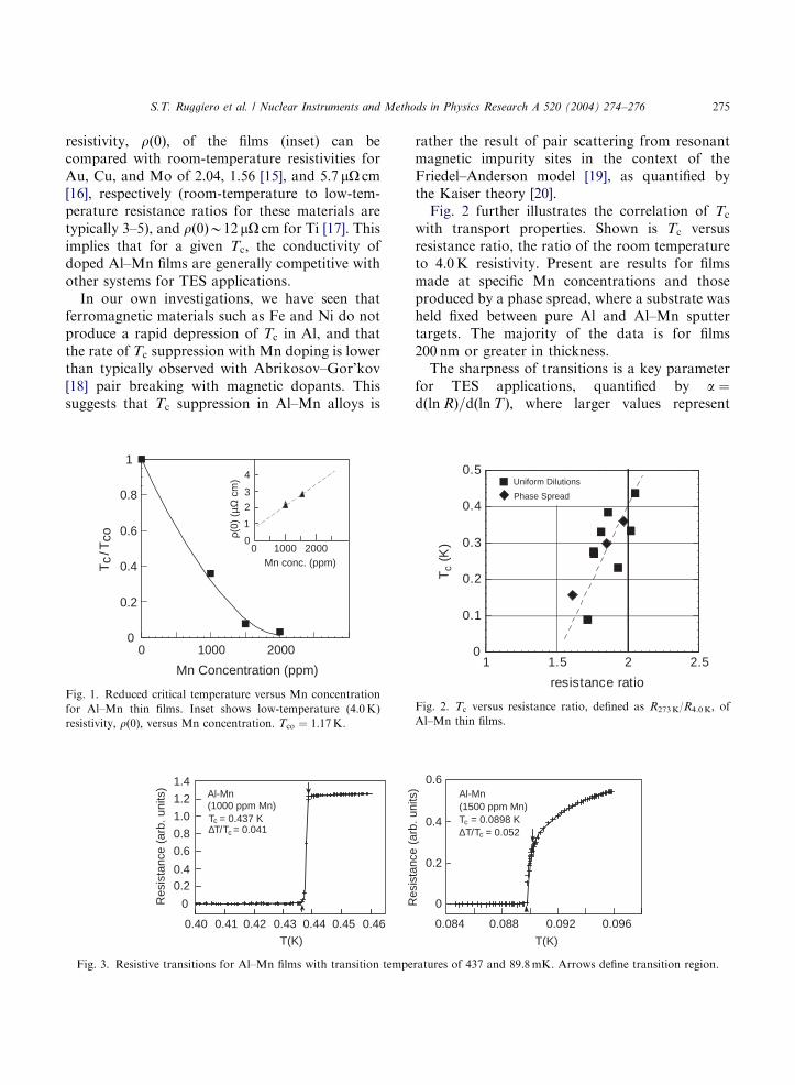
Shown in Fig. 1 is Tc versus Mn concentration,the latter established with Rutherford backscatter-ing. Results for the low-temperature (4.0 K)
d.
ARTICLE IN PRESS
S.T. Ruggiero et al. / Nuclear Instruments and Methods in Physics Research A 520 (2004) 274–276 275
resistivity, rð0Þ; of the films (inset) can becompared with room-temperature resistivities forAu, Cu, and Mo of 2.04, 1.56 [15], and 5.7 mO cm[16], respectively (room-temperature to low-tem-perature resistance ratios for these materials aretypically 3–5), and rð0ÞB12 mO cm for Ti [17]. Thisimplies that for a given Tc; the conductivity ofdoped Al–Mn films are generally competitive withother systems for TES applications.
In our own investigations, we have seen thatferromagnetic materials such as Fe and Ni do notproduce a rapid depression of Tc in Al, and thatthe rate of Tc suppression with Mn doping is lowerthan typically observed with Abrikosov–Gor’kov[18] pair breaking with magnetic dopants. Thissuggests that Tc suppression in Al–Mn alloys is
0
0.2
0.4
0.6
0.8
1
0 1000 2000
0
1
2
3
4
0 1000 2000Mn conc. (ppm)T
c/T
co ρ(0)
(µΩ
cm
)
Mn Concentration (ppm)
Fig. 1. Reduced critical temperature versus Mn concentration
for Al–Mn thin films. Inset shows low-temperature (4.0K)
resistivity, rð0Þ; versus Mn concentration. Tco ¼ 1:17K.
1.4
1.2
1.0
0.8
0.6
0.40.2
0
0.460.450.440.430.420.410.40
∆T/Tc = 0.041Tc = 0.437 K
Al-Mn(1000 ppm Mn)
T(K)
Res
ista
nce
(arb
. uni
ts)
Fig. 3. Resistive transitions for Al–Mn films with transition tempe
rather the result of pair scattering from resonantmagnetic impurity sites in the context of theFriedel–Anderson model [19], as quantified bythe Kaiser theory [20].
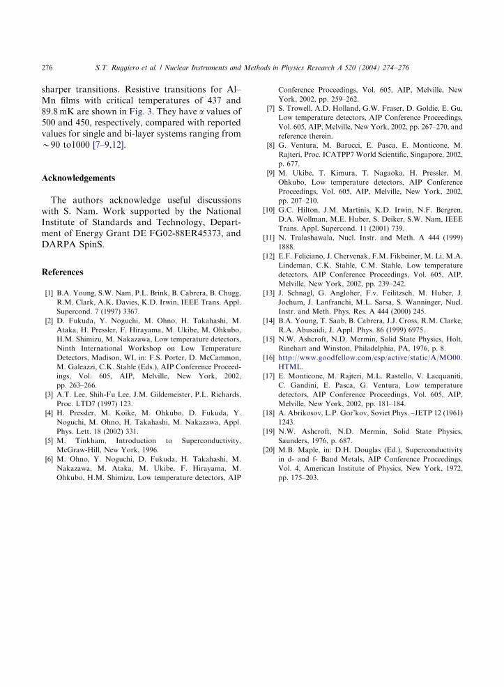
Fig. 2 further illustrates the correlation of Tc
with transport properties. Shown is Tc versusresistance ratio, the ratio of the room temperatureto 4.0 K resistivity. Present are results for filmsmade at specific Mn concentrations and thoseproduced by a phase spread, where a substrate washeld fixed between pure Al and Al–Mn sputtertargets. The majority of the data is for films200 nm or greater in thickness.
The sharpness of transitions is a key parameterfor TES applications, quantified by a ¼dðln RÞ=dðln TÞ; where larger values represent
0
0.1
0.2
0.3
0.4
0.5
1 1.5 2 2.5
Uniform Dilutions
Phase Spread
Tc
(K)
resistance ratio
Fig. 2. Tc versus resistance ratio, defined as R273K/R4.0 K, of
Al–Mn thin films.
0.6
0.4
0.2
0
0.0960.0920.0880.084
∆T/Tc = 0.052Tc = 0.0898 K
Al-Mn(1500 ppm Mn)
T(K)
Res
ista
nce
(arb
. uni
ts)
ratures of 437 and 89.8mK. Arrows define transition region.
ARTICLE IN PRESS
S.T. Ruggiero et al. / Nuclear Instruments and Methods in Physics Research A 520 (2004) 274–276276
sharper transitions. Resistive transitions for Al–Mn films with critical temperatures of 437 and89.8 mK are shown in Fig. 3. They have a values of500 and 450, respectively, compared with reportedvalues for single and bi-layer systems ranging fromB90 to1000 [7–9,12].
Acknowledgements
The authors acknowledge useful discussionswith S. Nam. Work supported by the NationalInstitute of Standards and Technology, Depart-ment of Energy Grant DE FG02-88ER45373, andDARPA SpinS.
References
[1] B.A. Young, S.W. Nam, P.L. Brink, B. Cabrera, B. Chugg,
R.M. Clark, A.K. Davies, K.D. Irwin, IEEE Trans. Appl.
Supercond. 7 (1997) 3367.
[2] D. Fukuda, Y. Noguchi, M. Ohno, H. Takahashi, M.
Ataka, H. Pressler, F. Hirayama, M. Ukibe, M. Ohkubo,
H.M. Shimizu, M. Nakazawa, Low temperature detectors,
Ninth International Workshop on Low Temperature
Detectors, Madison, WI, in: F.S. Porter, D. McCammon,
M. Galeazzi, C.K. Stahle (Eds.), AIP Conference Proceed-
ings, Vol. 605, AIP, Melville, New York, 2002,
pp. 263–266.
[3] A.T. Lee, Shih-Fu Lee, J.M. Gildemeister, P.L. Richards,
Proc. LTD7 (1997) 123.
[4] H. Pressler, M. Koike, M. Ohkubo, D. Fukuda, Y.
Noguchi, M. Ohno, H. Takahashi, M. Nakazawa, Appl.
Phys. Lett. 18 (2002) 331.
[5] M. Tinkham, Introduction to Superconductivity,
McGraw-Hill, New York, 1996.
[6] M. Ohno, Y. Noguchi, D. Fukuda, H. Takahashi, M.
Nakazawa, M. Ataka, M. Ukibe, F. Hirayama, M.
Ohkubo, H.M. Shimizu, Low temperature detectors, AIP
Conference Proceedings, Vol. 605, AIP, Melville, New
York, 2002, pp. 259–262.
[7] S. Trowell, A.D. Holland, G.W. Fraser, D. Goldie, E. Gu,
Low temperature detectors, AIP Conference Proceedings,
Vol. 605, AIP, Melville, New York, 2002, pp. 267–270, and
reference therein.
[8] G. Ventura, M. Barucci, E. Pasca, E. Monticone, M.
Rajteri, Proc. ICATPP7 World Scientific, Singapore, 2002,
p. 677.
[9] M. Ukibe, T. Kimura, T. Nagaoka, H. Pressler, M.
Ohkubo, Low temperature detectors, AIP Conference
Proceedings, Vol. 605, AIP, Melville, New York, 2002,
pp. 207–210.
[10] G.C. Hilton, J.M. Martinis, K.D. Irwin, N.F. Bergren,
D.A. Wollman, M.E. Huber, S. Deiker, S.W. Nam, IEEE
Trans. Appl. Supercond. 11 (2001) 739.
[11] N. Tralashawala, Nucl. Instr. and Meth. A 444 (1999)
1888.
[12] E.F. Feliciano, J. Chervenak, F.M. Fikbeiner, M. Li, M.A.
Lindeman, C.K. Stahle, C.M. Stahle, Low temperature
detectors, AIP Conference Proceedings, Vol. 605, AIP,
Melville, New York, 2002, pp. 239–242.
[13] J. Schnagl, G. Angloher, F.v. Feilitzsch, M. Huber, J.
Jochum, J. Lanfranchi, M.L. Sarsa, S. Wanninger, Nucl.
Instr. and Meth. Phys. Res. A 444 (2000) 245.
[14] B.A. Young, T. Saab, B. Cabrera, J.J. Cross, R.M. Clarke,
R.A. Abusaidi, J. Appl. Phys. 86 (1999) 6975.
[15] N.W. Ashcroft, N.D. Mermin, Solid State Physics, Holt,
Rinehart and Winston, Philadelphia, PA, 1976, p. 8.
[16] http://www.goodfellow.com/csp/active/static/A/MO00.
HTML.
[17] E. Monticone, M. Rajteri, M.L. Rastello, V. Lacquaniti,
C. Gandini, E. Pasca, G. Ventura, Low temperature
detectors, AIP Conference Proceedings, Vol. 605, AIP,
Melville, New York, 2002, pp. 181–184.
[18] A. Abrikosov, L.P. Gor’kov, Soviet Phys. –JETP 12 (1961)
1243.
[19] N.W. Ashcroft, N.D. Mermin, Solid State Physics,
Saunders, 1976, p. 687.
[20] M.B. Maple, in: D.H. Douglas (Ed.), Superconductivity
in d- and f- Band Metals, AIP Conference Proceedings,
Vol. 4, American Institute of Physics, New York, 1972,
pp. 175–203.