Embed Size (px)
Citation preview
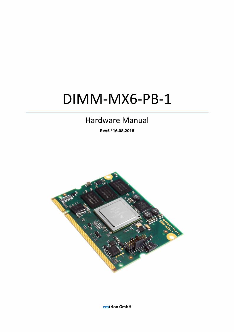
DIMM-MX6-PB-1 Hardware Manual
Rev5 / 16.08.2018
emtrion GmbH
DIMM-MX6-PB-1(Rev5) 2/34
© Copyright 2018 emtrion GmbH
All rights reserved. This documentation may not be photocopied or recorded on any electronic
media without written approval. The information contained in this documentation is subject to
change without prior notice. We assume no liability for erroneous information or its consequences.
Trademarks used from other companies refer exclusively to the products of those companies.
Revision: 5 / 16.08.2018 Rev Date/Signature Changes
1 25.04.2018/Bue First revision 2 01.06.2018/Bue Corrected I2C2 usage and PMIC 3 20.06.2018/Bue Processor Bus settings corrected 4 14.08.2018/We Description of GPIO7 corrected in chapters 4.18, 5.1 and 6.1 5 16.08.2018/Bue 3 spare GPIOs added in chapter 4.18
SPI and Audio pin description corrected in chapter 6.1
DIMM-MX6-PB-1(Rev5) 3/34
Contents
1 Introduction ................................................................................................................................................................ 5
2 Block Diagram ............................................................................................................................................................ 6
3 Handling Precautions .............................................................................................................................................. 7
4 Functional Description ........................................................................................................................................... 8
4.1 Processor ............................................................................................................................................................. 8
4.1.1 Processor Clocks ..................................................................................................................................... 9
4.1.2 Boot Mode ................................................................................................................................................ 9
4.2 NOR-Flash ........................................................................................................................................................... 9
4.3 NAND-Flash ........................................................................................................................................................ 9
4.4 DDR3 SDRAM .................................................................................................................................................. 10
4.5 Processor Bus.................................................................................................................................................. 10
4.6 Ethernet ............................................................................................................................................................ 10
4.7 USB Host ........................................................................................................................................................... 11
4.8 USB Device ...................................................................................................................................................... 11
4.9 Graphic Displays ............................................................................................................................................ 11
4.9.1 LVDS ......................................................................................................................................................... 12
4.9.2 HDMI ........................................................................................................................................................ 13
4.10 Touch Interface .............................................................................................................................................. 13
4.11 Audio Interface .............................................................................................................................................. 13
4.12 SD-Card Interface .......................................................................................................................................... 13
4.13 Serial Ports ....................................................................................................................................................... 14
4.14 I²C- Bus .............................................................................................................................................................. 14
4.15 SPI Interface .................................................................................................................................................... 14
4.16 CAN .................................................................................................................................................................... 15
4.17 SATA .................................................................................................................................................................. 15
4.18 General Purpose I/Os ................................................................................................................................... 15
4.19 DIP Switches, Status LED ............................................................................................................................ 16
4.20 Interrupts ......................................................................................................................................................... 16
4.21 Reset .................................................................................................................................................................. 16
4.22 Power Supply ................................................................................................................................................. 17
4.23 Connectors ...................................................................................................................................................... 18
4.23.1 SODIMM Connector ........................................................................................................................... 18
4.23.2 Extension Connector .......................................................................................................................... 18
4.23.3 Debug Connector ................................................................................................................................ 18
5 Pin Assignments ..................................................................................................................................................... 19
5.1 J1, SODIMM ..................................................................................................................................................... 19
5.2 J3, Extension Connector 2 ......................................................................................................................... 22
5.3 J4, Debug Connector ................................................................................................................................... 23
6 Signal Characteristics ........................................................................................................................................... 24
6.1 J1, SODIMM Connector ............................................................................................................................... 24
6.2 J3, Extension Connector ............................................................................................................................. 30
6.3 J4, Debug Connector ................................................................................................................................... 31
DIMM-MX6-PB-1(Rev5) 4/34
7 Technical Characteristics .................................................................................................................................... 32
7.1 Electrical Specifications .............................................................................................................................. 32
7.2 Environmental Specifications ................................................................................................................... 32
7.3 Mechanical Specifications ......................................................................................................................... 32
8 Dimensional Drawing .......................................................................................................................................... 33
9 References ................................................................................................................................................................ 34
DIMM-MX6-PB-1(Rev5) 5/34
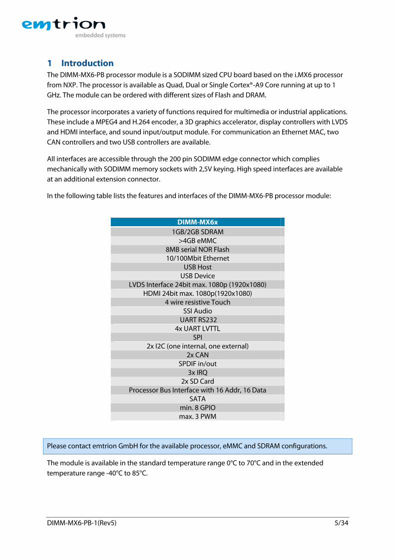
1 Introduction The DIMM-MX6-PB processor module is a SODIMM sized CPU board based on the i.MX6 processor
from NXP. The processor is available as Quad, Dual or Single Cortex®-A9 Core running at up to 1
GHz. The module can be ordered with different sizes of Flash and DRAM.
The processor incorporates a variety of functions required for multimedia or industrial applications.
These include a MPEG4 and H.264 encoder, a 3D graphics accelerator, display controllers with LVDS
and HDMI interface, and sound input/output module. For communication an Ethernet MAC, two
CAN controllers and two USB controllers are available.
All interfaces are accessible through the 200 pin SODIMM edge connector which complies
mechanically with SODIMM memory sockets with 2,5V keying. High speed interfaces are available
at an additional extension connector.
In the following table lists the features and interfaces of the DIMM-MX6-PB processor module:
DIMM-MX6x
1GB/2GB SDRAM >4GB eMMC
8MB serial NOR Flash 10/100Mbit Ethernet
USB Host USB Device
LVDS Interface 24bit max. 1080p (1920x1080) HDMI 24bit max. 1080p(1920x1080)
4 wire resistive Touch SSI Audio
UART RS232 4x UART LVTTL
SPI 2x I2C (one internal, one external)
2x CAN SPDIF in/out
3x IRQ 2x SD Card
Processor Bus Interface with 16 Addr, 16 Data SATA
min. 8 GPIO max. 3 PWM
Please contact emtrion GmbH for the available processor, eMMC and SDRAM configurations.
The module is available in the standard temperature range 0°C to 70°C and in the extended
temperature range -40°C to 85°C.
DIMM-MX6-PB-1(Rev5) 6/34
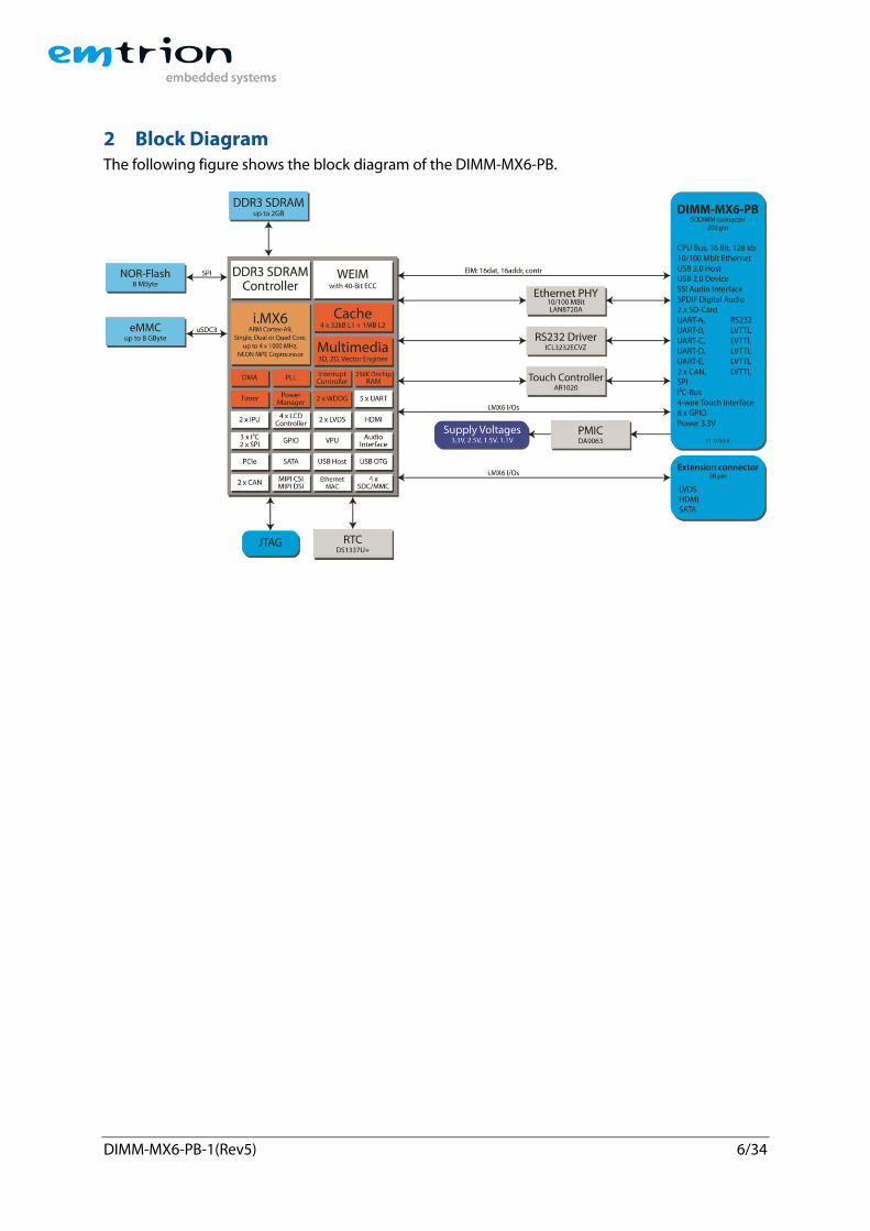
2 Block Diagram The following figure shows the block diagram of the DIMM-MX6-PB.
DIMM-MX6-PB-1(Rev5) 7/34
3 Handling Precautions Please read the following notes prior to installing the DIMM-MX6-PB processor module. They apply
to all ESD (electrostatic discharge) sensitive components:
The DIMM-MX6x does not need any configurations before installation.
The module does not provide any on-board ESD protection circuitry – this must be
provided by the product it is used in.
Before installing the module it is recommended that you discharge yourself by touching a
grounded object.
Be sure all tools required for installation are electrostatically discharged as well.
Before installing (or removing) the module, unplug the power cable from your mains
supply.
Handle the board with care and try to avoid touching its components or tracks.
DIMM-MX6-PB-1(Rev5) 8/34
4 Functional Description
4.1 Processor
The DIMM-MX6-PB processor module uses the processor i.MX6x from NXP [1]. It includes up to 4
ARM Cortex® A9 cores and runs up to 1 GHz.
In addition to the CPU core with MMU, FPU and Caches, this processor provides a lot of features
such as:
NAND Flash controller
DDR3 SDRAM controller
Ethernet MAC 10/100Mbit with IEEE1588 support
USB 2.0 Host with high-speed mode
USB 2.0 OTG with high-speed mode
2 SD Card host controllers
Two Image Processing Units which includes
o Two Video input modules with camera capturing module
o LCD Controller for TFT displays up to 1080p (1920x1080) @60Hz and 16/18/24 bpp
o 24bit LVDS display port up to WXGA (1366x768) @60Hz and 16/18/24 bpp
o 24bit HDMI port up to 1080p (1920x1080) @60Hz and 16/18/24 bpp
o 2D and 3D graphic hardware accelerator
o NEON SIMD media accelerator
4 wire Touch controller
Two CAN controllers
5 UARTs with 2x 32 byte FIFO
I2C bus interfaces
SPI interfaces
IrDA interfaces
Watchdog timer
Real time clock
Sound interface with I2S format
Sound interface SPDIF in and out
SATA controller
32-bit timer
JTAG debug interface
Further details of the processor can be found in the i.MX6x Reference Manual [1].
DIMM-MX6-PB-1(Rev5) 9/34
4.1.1 Processor Clocks
The 24MHz main clock is generated by a crystal. Eight internal PLLs multiply the 24 MHz main clock
to generate the internal clocks. All clocks within the processor are derived from theses frequencies,
via various software configurable dividers.
The core clock (PLL1) can be up to 1.2 GHz. For power management, the core clock can be varied.
It must be considered that the core voltage should be adapted if the core frequency is varied.
More information about the i.MX6 clock system is described in the CCM chapter of the i.MX6
Reference Manual [1].
The RTC_XTALI clock input of the CPU is supplied by a 32.768 kHz clock from the RTC chip. That RTC
chip is connected to a 32.768 kHz crystal. This clock swings even when the main supply is switched
off and an auxiliary voltage (2,3V – 3,3V) is connected at the BAT pin of the SODIMM connector.
4.1.2 Boot Mode
The DIMM-MX6x Uboot can be booted either from the onboard serial NOR-Flash or external via the
USB Device interface. The boot mode is configured via the DIP Switch SW1.
SW1-1 SW1-2 Boot source
0 (OFF) 1 (ON) Serial NOR-Flash 1 (ON) 0 (OFF) (USB) Serial
4.2 NOR-Flash
An 8 MB serial NOR flash of type MX25L6445 from Macronix is used as primary boot device. It is
connected to the interface ECSPI4.
The integrated i.MX6 bootloader is configured for booting from the serial NOR flash. Booting from
NOR Flash is enabled if the DIP switch SW1-1 is OFF and SW1-2 is ON.
Besides the Uboot module specific configuration data, like a MAC address, the serial number etc,
are also stored in the serial NOR Flash.
Hardware write protection of the NOR flash is realized by the port pin GPIO6-11 of the i.MX6. A low
level protects the flash device. During and after Reset the pin is driven low by the processor.
Besides the hardware protection the chip also supports a software protection.
4.3 NAND-Flash
To store the operating system and application data, an eMMC is used on the DIMM-MX6-PB
module. It is connected to the SDHC3 interface of the processor with 8 data lines. The signalling
level is fixed at 3.3V therefore higher data rates are not supported.
The eMMC is reset either by the global reset signal RESO#, by SDHC3 reset function or GPIO7-8 if
the pin SD3_RST is configured as a GPIO output. A low level at the signal SD3_RST resets the eMMC.
DIMM-MX6-PB-1(Rev5) 10/34
By default a eMMC with 4 GB capacity is fit.
4.4 DDR3 SDRAM DDR3 SDRAM is available as main memory. The RAM memory has a 64bit width interface and is
clocked with 528MHz.
The SDRAM size can be selected between 512MB and 2GB, depending on the ordering code. The
following table shows the address range of the different RAM sizes.
RAM size Start address End address
512MB 0x10000000 0x2FFFFFFF 1GB 0x10000000 0x4FFFFFFF 2GB 0x10000000 0x8FFFFFFF
Please contact emtrion GmbH for your required RAM size.
4.5 Processor Bus
The processor bus interface of the iMX6 is routed to the SODIMM connector. The interface is
realized as an asynchronous SRAM interface with 16 bit data and 16 addresses lines. 32 MHz clock,
control signals and one chip select signal are also routed to the SODIMM connector.
The address space is in the range 0x08000000 … 0x0801FFFF.
The following table describes the processor bus interface signals.
Signal Description
A[15:0]* Address bus D[15:0] Data bus
CKIO 32 MHz bus clock WAIT# active low wait input signal
CS# active low chip select RD# active low read signal
WE0# active low selection for lower data byte D[7:0] WE1# active low selection for higher data byte D[15:8]
RD/WR# Low active write enable signal
* These signals are used as boot configuration pins during reset. During reset these signals must
not be driven externally.
4.6 Ethernet The Ethernet interface is realized with the processor internal Media Access Controller (MAC) and an
external Physical Layer Interface (PHY) LAN8720A from SMSC. An RMII interface is used for
communication between the MAC and the PHY.
DIMM-MX6-PB-1(Rev5) 11/34
The Ethernet interface supports the operating modes 100BASE-TX or 10BASE-T, both half- and full
duplex. HP Auto-MDIX is also supported.
The registers of the Ethernet PHY are accessed via the Media Independent Interface (MII).
The Ethernet signal lines (ETH_TDP, ETH_TDM, ETH_RDP, ETH_RDM) as well as two LED status
signals (SPEED_LED#, LINK_LED#) that indicate the link status and the transfer speed are connected
to the SODIMM connector. An appropriate transformer must be added externally.
The signal LINK_LED# indicates if data packages are transferred. (“0” = traffic). The signal is an open
drain output signal.
The signal SPEED_LED# indicates if the data is transferred with 100Mbit/s. (“0” = 100Mbit/s). The
signal is an open drain output signal.
The RMII 50MHz Ethernet clock is generated by the PLL6 (ENET PLL) of the i.MX6 and it is routed to
the processor internal MAC and to Ethernet PHY.
The Ethernet PHY can be reset either by the global reset signal RESO# or by the GPIO7-9 if the i.MX6
pin SD4_CMD is configured as a GPIO output. A low at this pin resets the Ethernet PHY.
4.7 USB Host The USB Host interface is realized by the internal host controller of the i.MX6x. The interface is USB
2.0 compliant, supporting data transfer rates low-speed (1,5Mbps), full-speed (12 Mbps) and high-
speed (480Mbps).
To switch VBUS supply the control line USBH_PEN# is connected to the SODIMM connector. A
logical “0” at the processor GPIO3-31 switches the power on. The signal USBH_OC# reports an
overcurrent from the power switch at the pin GPIO3-30 (“0” = overcurrent).
The data lines and the control lines are available at the SODIMM connector. A USB power switch
must be added externally. The data lines are internally terminated with 15-K pulldown resistors.
The external VBUS signal must be fed back to the pin USBH_VBUS of the SODIMM connector.
4.8 USB Device The USB Device interface is realized by the internal device controller of the i.MX6x. The interface is
USB 2.0 compliant, supporting data transfers at low-speed (1,5Mbps), full-speed (12 Mbps) and
high-speed (480Mbps).
The data lines and the control line USBF_VBUS are available at the SODIMM connector.
4.9 Graphic Displays The DIMM-MX6-PB has two display ports. The first is a 24bit HDMI display port and the second is a
24bit LVDS display port.
DIMM-MX6-PB-1(Rev5) 12/34
The i.MX6 includes two Image Processing Units (IPU). One IPU can display up to two different
images. Maximum four independent images can be displayed on the two available display ports.
This can be configured via software.
More information about the i.MX6 Multimedia system is described in the Multimedia and IPU
chapter of the i.MX6 Reference Manual [1].
4.9.1 LVDS
The LCD controller of the i.MX6x can drive the LVDS interface with resolutions up to FullHD
(1920x1080) at 16/18/24bpp. The pixel clock for the display data can be generated by an internal
clock or via the external LCD_CLK_IN.
The LVDS interface can be used by both IPU1 display units (IPU1_DI0 and IPU1_DI1) and both IPU2
display units (IPU2_DI0 and IPU2_DI1).
The LVDS lines are available at the extension connector J3. The following table list the LVDS signals:
signal Description
LVDS_CLK_P/N Differential LVDS clock LVDS_TX0_P/N First differential LVDS data signal pair LVDS_TX1_P/N Second differential LVDS data signal pair LVDS_TX2_P/N Third differential LVDS data signal pair LVDS_TX3_P/N Fourth differential LVDS data signal pair;
Only used in 24bit mode
In 24 bit mode the colour mapping can be changed depending of the used display. The following
table shows the default 18/24bit colour mapping in the SPWG/PSWG/VESA mode.
signal Slot0 Slot1 Slot2 Slot3 Slot4 Slot5 Slot6
LVDS_TX0 G0 R5 R4 R3 R2 R1 R0 LVDS_TX1 B1 B0 G5 G4 G3 G2 G1 LVDS_TX2 DE VS HS B5 B4 B3 B2
LVDS_TX3 (only for 24bit) CTL B7 B6 G7 G6 R7 R6
The following table shows the 24bit colour mapping in the JEIDA mode.
signal Slot0 Slot1 Slot2 Slot3 Slot4 Slot5 Slot6
LVDS_TX0 G2 R7 R6 R5 R4 R3 R2 LVDS_TX1 B3 B2 G7 G6 G5 G4 G3 LVDS_TX2 DE VS HS B7 B6 B5 B4 LVDS_TX3 CTL B1 B0 G1 G0 R1 R0
DIMM-MX6-PB-1(Rev5) 13/34
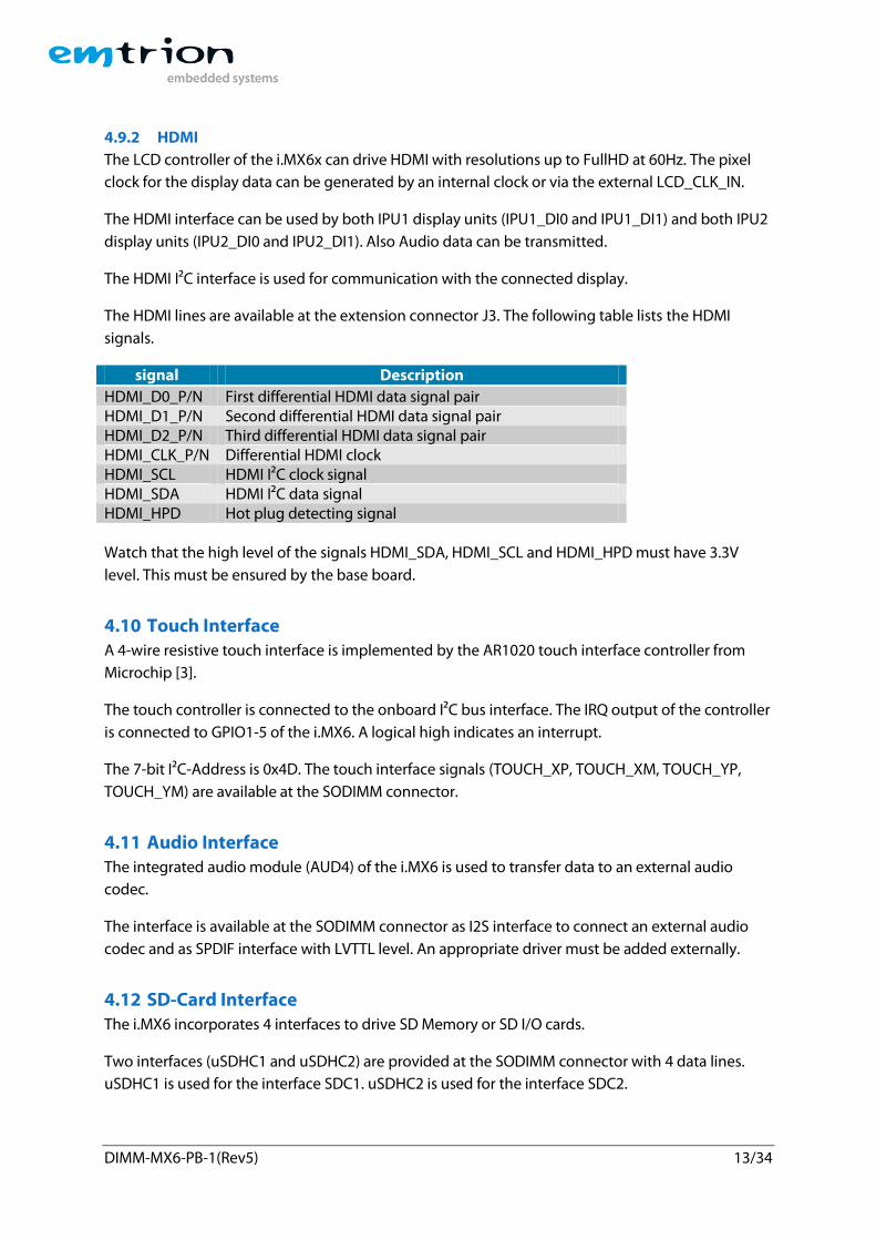
4.9.2 HDMI
The LCD controller of the i.MX6x can drive HDMI with resolutions up to FullHD at 60Hz. The pixel
clock for the display data can be generated by an internal clock or via the external LCD_CLK_IN.
The HDMI interface can be used by both IPU1 display units (IPU1_DI0 and IPU1_DI1) and both IPU2
display units (IPU2_DI0 and IPU2_DI1). Also Audio data can be transmitted.
The HDMI I²C interface is used for communication with the connected display.
The HDMI lines are available at the extension connector J3. The following table lists the HDMI
signals.
signal Description
HDMI_D0_P/N First differential HDMI data signal pair HDMI_D1_P/N Second differential HDMI data signal pair HDMI_D2_P/N Third differential HDMI data signal pair HDMI_CLK_P/N Differential HDMI clock HDMI_SCL HDMI I²C clock signal HDMI_SDA HDMI I²C data signal HDMI_HPD Hot plug detecting signal Watch that the high level of the signals HDMI_SDA, HDMI_SCL and HDMI_HPD must have 3.3V
level. This must be ensured by the base board.
4.10 Touch Interface A 4-wire resistive touch interface is implemented by the AR1020 touch interface controller from
Microchip [3].
The touch controller is connected to the onboard I²C bus interface. The IRQ output of the controller
is connected to GPIO1-5 of the i.MX6. A logical high indicates an interrupt.
The 7-bit I²C-Address is 0x4D. The touch interface signals (TOUCH_XP, TOUCH_XM, TOUCH_YP,
TOUCH_YM) are available at the SODIMM connector.
4.11 Audio Interface The integrated audio module (AUD4) of the i.MX6 is used to transfer data to an external audio
codec.
The interface is available at the SODIMM connector as I2S interface to connect an external audio
codec and as SPDIF interface with LVTTL level. An appropriate driver must be added externally.
4.12 SD-Card Interface The i.MX6 incorporates 4 interfaces to drive SD Memory or SD I/O cards.
Two interfaces (uSDHC1 and uSDHC2) are provided at the SODIMM connector with 4 data lines.
uSDHC1 is used for the interface SDC1. uSDHC2 is used for the interface SDC2.
DIMM-MX6-PB-1(Rev5) 14/34
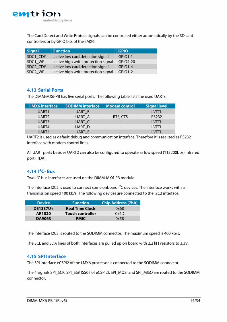
The Card Detect and Write Protect signals can be controlled either automatically by the SD card
controllers or by GPIO bits of the i.MX6:
Signal Function GPIO
SDC1_CD# active low card detection signal GPIO1-1 SDC1_WP active high write protection signal GPIO4-20 SDC2_CD# active low card detection signal GPIO1-4 SDC2_WP active high write protection signal GPIO1-2
4.13 Serial Ports The DIMM-MX6-PB has five serial ports. The following table lists the used UARTs:
i.MX6 interface SODIMM interface Modem control Signal level
UART1 UART_B - LVTTL UART2 UART_A RTS, CTS RS232 UART3 UART_C - LVTTL UART4 UART_D - LVTTL UART5 UART_E - LVTTL
UART2 is used as default debug and communication interface. Therefore it is realized as RS232
interface with modem control lines.
All UART ports besides UART2 can also be configured to operate as low speed (115200bps) Infrared
port (IrDA).
4.14 I²C- Bus Two I²C bus interfaces are used on the DIMM-MX6-PB module.
The interface I2C2 is used to connect some onboard I²C devices. The interface works with a
transmission speed 100 kb/s. The following devices are connected to the I2C2 interface:
Device Function Chip Address (7bit)
DS1337U+ Real Time Clock 0x68 AR1020 Touch controller 0x4D DA9063 PMIC 0x58
The interface I2C3 is routed to the SODIMM connector. The maximum speed is 400 kb/s.
The SCL and SDA lines of both interfaces are pulled up on board with 2.2 k resistors to 3.3V.
4.15 SPI Interface The SPI interface eCSPI2 of the i.MX6 processor is connected to the SODIMM connector.
The 4 signals SPI_SCK, SPI_SS# (SS0# of eCSPI2), SPI_MOSI and SPI_MISO are routed to the SODIMM
connector.
DIMM-MX6-PB-1(Rev5) 15/34
4.16 CAN The i.MX6 processor includes two CAN controllers, which comply with the CAN protocol
specification 2.0B, supporting both standard and extended message frames.
The TX and RX signals are routed to the SODIMM connector as LVTTL signals. A CAN transceiver
must be added externally. The maximum baud rate is 1Mbps.
4.17 SATA The i.MX6x includes a SATA controller and a SATA phy. The SATA controller is compliant with the
SATA specification 3.0 at 1,5Gb/s and 3,0Gb/s.
The SATA signals are routed to the extension connector J3. The AC coupling capacitors are located
on the DIMM-MX6-PB module.
More details of the SATA controller can be found in the i.MX6x Reference Manual [1].
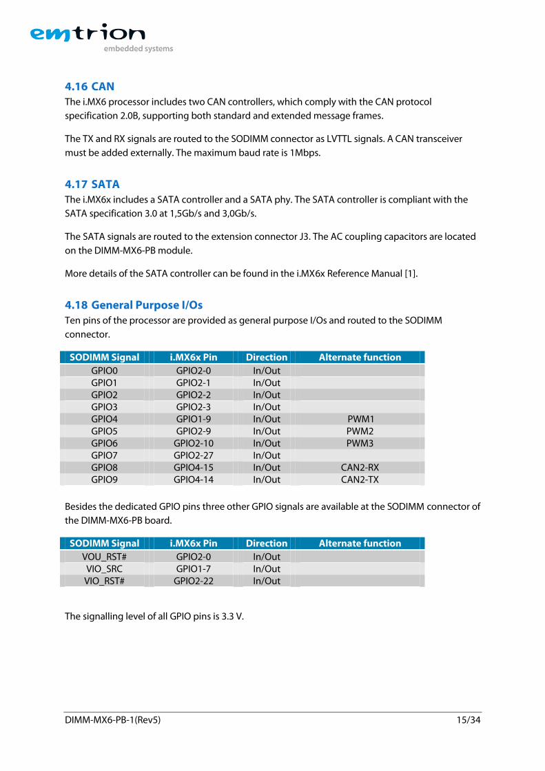
4.18 General Purpose I/Os Ten pins of the processor are provided as general purpose I/Os and routed to the SODIMM
connector.
SODIMM Signal i.MX6x Pin Direction Alternate function
GPIO0 GPIO2-0 In/Out GPIO1 GPIO2-1 In/Out GPIO2 GPIO2-2 In/Out GPIO3 GPIO2-3 In/Out GPIO4 GPIO1-9 In/Out PWM1 GPIO5 GPIO2-9 In/Out PWM2 GPIO6 GPIO2-10 In/Out PWM3 GPIO7 GPIO2-27 In/Out GPIO8 GPIO4-15 In/Out CAN2-RX GPIO9 GPIO4-14 In/Out CAN2-TX
Besides the dedicated GPIO pins three other GPIO signals are available at the SODIMM connector of
the DIMM-MX6-PB board.
SODIMM Signal i.MX6x Pin Direction Alternate function
VOU_RST# GPIO2-0 In/Out VIO_SRC GPIO1-7 In/Out VIO_RST# GPIO2-22 In/Out
The signalling level of all GPIO pins is 3.3 V.
DIMM-MX6-PB-1(Rev5) 16/34
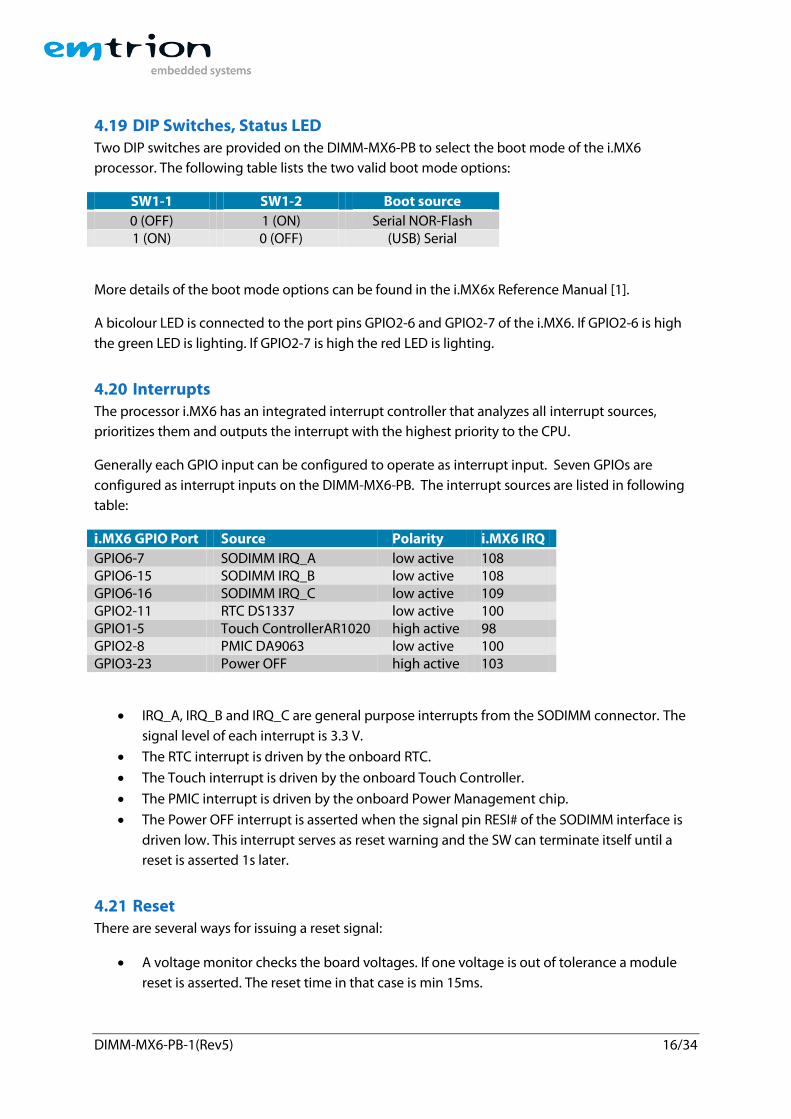
4.19 DIP Switches, Status LED Two DIP switches are provided on the DIMM-MX6-PB to select the boot mode of the i.MX6
processor. The following table lists the two valid boot mode options:
SW1-1 SW1-2 Boot source
0 (OFF) 1 (ON) Serial NOR-Flash 1 (ON) 0 (OFF) (USB) Serial
More details of the boot mode options can be found in the i.MX6x Reference Manual [1].
A bicolour LED is connected to the port pins GPIO2-6 and GPIO2-7 of the i.MX6. If GPIO2-6 is high
the green LED is lighting. If GPIO2-7 is high the red LED is lighting.
4.20 Interrupts The processor i.MX6 has an integrated interrupt controller that analyzes all interrupt sources,
prioritizes them and outputs the interrupt with the highest priority to the CPU.
Generally each GPIO input can be configured to operate as interrupt input. Seven GPIOs are
configured as interrupt inputs on the DIMM-MX6-PB. The interrupt sources are listed in following
table:
i.MX6 GPIO Port Source Polarity i.MX6 IRQ
GPIO6-7 SODIMM IRQ_A low active 108 GPIO6-15 SODIMM IRQ_B low active 108 GPIO6-16 SODIMM IRQ_C low active 109 GPIO2-11 RTC DS1337 low active 100 GPIO1-5 Touch ControllerAR1020 high active 98 GPIO2-8 PMIC DA9063 low active 100 GPIO3-23 Power OFF high active 103
IRQ_A, IRQ_B and IRQ_C are general purpose interrupts from the SODIMM connector. The
signal level of each interrupt is 3.3 V.
The RTC interrupt is driven by the onboard RTC.
The Touch interrupt is driven by the onboard Touch Controller.
The PMIC interrupt is driven by the onboard Power Management chip.
The Power OFF interrupt is asserted when the signal pin RESI# of the SODIMM interface is
driven low. This interrupt serves as reset warning and the SW can terminate itself until a
reset is asserted 1s later.
4.21 Reset There are several ways for issuing a reset signal:
A voltage monitor checks the board voltages. If one voltage is out of tolerance a module
reset is asserted. The reset time in that case is min 15ms.
DIMM-MX6-PB-1(Rev5) 17/34
The active low signal RESI# at the SODIMM connector and the signal JTAG_RESI# at the
debug connector, can assert a reset if this signal is asserted longer than 1s. Immediately
after the falling edge a Power OFF interrupt is asserted, that can be used by the SW to shut
down itself until the reset is asserted.
A processor internal SW reset is available at a processor pin, if the pin function SYSTEM_RST
is enabled. In that case the RESO# pin is asserted if a SW reset is asserted.
All resets are hardware resets of the whole board. All resets except the internal SW reset issue a
processor cold reset. The internal SW reset issues a processor warm reset.
The duration of the reset signal is min. 15ms. For resetting external devices the reset signal is
available as an output (RESO#) at the SODIMM connector.
4.22 Power Supply The typical power consumption (all 4 cores) is 1,5A (tbc) at +3,3V, +/- 5%, which must be supplied
via the SODIMM connector. The onboard required voltages for the processor and the other parts
are generated on board via a Power Management (PMIC) chip and the i.MX6 processor. The PMIC
generates the input voltages for the i.MX6. The i.MX6 internal LDO’s generate the power supply
voltages for the i.MX6 cores and modules.
The voltages generated by the PMIC can be configured via the I²C interface. The voltages
generated by the i.MX6 can be configured via processor internal registers. During operation the
voltages can be varied depending on the core frequencies and die temperature.
More details about DVFS (Dynamic Voltage and Frequency Scaling) and power supply variation are
described in the chapter 26 of the i.MX6 Reference Manual [1].
The SODIMM BAT pin is the battery input pin for the RTC power supply. The typical power
consumption of the RTC via the BAT pin is < 1µA.
DIMM-MX6-PB-1(Rev5) 18/34
4.23 Connectors The module DIMM-MX6-PB incorporates three connectors. J1 is the SODIMM connector, J3 is an
extension connector and J4 is the JTAG debug connector.
The connector J3 is located on the bottom side of the CPU module.
4.23.1 SODIMM Connector
Most signals of the board are available at the SODIMM connector.
The DIMM interface is a 200 pos SODIMM connector that fits mechanically into a regular DDR1
SODIMM memory socket with 2,5V keying. These sockets are available from various manufacturers.
Usage details of the connector and its electrical and mechanical characteristics can be found in
following chapter 5.1 of this document.
Notes:
The pin out of the SODIMM connector is NOT compatible with memory sockets. Insertion into a
socket with wrong pin out may damage the DIMM-MX6-PB and the carrier board.
Most of the pins are directly connected with the processor i.MX6.
4.23.2 Extension Connector
The serial high speed interfaces LVDS, SATA and HDMI are routed to the extension connector J3.
More details about the pin assignment and the connector types are described in chapter 5.2. The
signal characteristics are described in chapter Fehler! Verweisquelle konnte nicht gefunden
erden..
4.23.3 Debug Connector
All ARM debug interface and the Boot Mode signals are available at the 20 pin header J4.
Please contact emtrion GmbH for further details how to connect an emulator to J4.
DIMM-MX6-PB-1(Rev5) 19/34
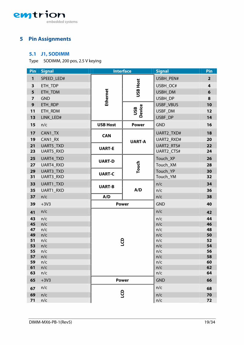
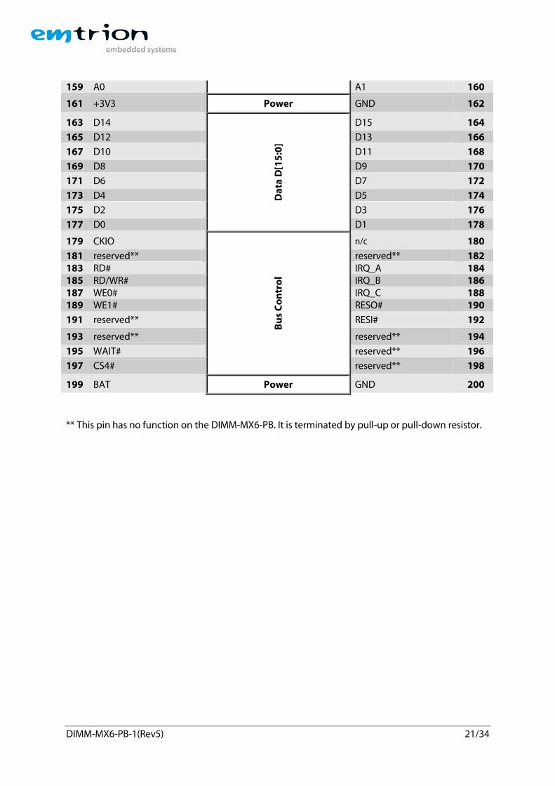
5 Pin Assignments
5.1 J1, SODIMM
Type SODIMM, 200 pos, 2.5 V keying
Pin Signal Interface Signal Pin
1 SPEED_LED#
Eth
ern
et
US
B H
ost
USBH_PEN# 2
3 ETH_TDP USBH_OC# 4
5 ETH_TDM USBH_DM 6
7 GND USBH_DP 8
9 ETH_RDP
US
B
De
vic
e USBF_VBUS 10
11 ETH_RDM USBF_DM 12
13 LINK_LED# USBF_DP 14
15 n/c USB Host Power GND 16
17 CAN1_TX CAN
UART-A
UART2_TXD# 18
19 CAN1_RX UART2_RXD# 20
21 UART5_TXD UART-E
UART2_RTS# 22 23 UART5_RXD UART2_CTS# 24
25 UART4_TXD UART-D
To
uch
Touch_XP 26
27 UART4_RXD Touch_XM 28
29 UART3_TXD UART-C
Touch_YP 30 31 UART3_RXD Touch_YM 32
33 UART1_TXD UART-B
A/D
n/c 34
35 UART1_RXD n/c 36
37 n/c A/D n/c 38
39 +3V3 Power GND 40
41 n/c
LC
D
n/c 42
43 n/c n/c 44 45 n/c n/c 46 47 n/c n/c 48 49 n/c n/c 50 51 n/c n/c 52 53 n/c n/c 54 55 n/c n/c 56 57 n/c n/c 58 59 n/c n/c 60 61 n/c n/c 62 63 n/c n/c 64
65 +3V3 Power GND 66
67 n/c
LC
D n/c 68
69 n/c n/c 70 71 n/c n/c 72
DIMM-MX6-PB-1(Rev5) 20/34
73 n/c n/c 74 75 n/c n/c 76
77 VOU_RST#*
CS
I1
n/c 78
79 n/c n/c 80 81 n/c n/c 82 83 n/c n/c 84 85 n/c n/c 86 87 n/c n/c 88 89 VIO_SRC n/c 90 91 VIO_RST# n/c 92
93 +3V3 Power GND 94
95 SDC2_D0 S
DC
2
SD
C1
SDC1_D0 96
97 SDC2_D1 SDC1_D1 98 99 SDC2_D2 SDC1_D2 100
101 SDC2_D3 SDC1_D3 102 103 SDC2_CMD SDC1_CMD 104 105 SDC2_CLK SDC1_CLK 106 107 SDC2_CD# SDC1_CD# 108 109 SDC2_WP SDC1_WP 110
111 SPI_SS# SPI
SPI_MISO 112
113 SPI_SCK SPI_MOSI 114
115 I2C3_SCL
I2C
Au
dio
AUDIO_BCK 116
117 I2C3_SDA AUDIO_LRC 118
119 SPDIF_IN
SP
DIF
AUDIO_DATI 120 121 SPDIF_OUT AUDIO_DATO 122
123 GND Power n/c 124
125 CAN2_RX
GP
IO
CAN2_TX 126
127 GPIO6 GPIO7 128
129 GPIO4 GPIO5 130 131 GPIO2 GPIO3 132 133 GPIO0 GPIO1 134
135 +3V3 Power GND 136
137 n/c
Ad
dre
ss A
[23
:0]
n/c 138
139 n/c n/c 140
141 n/c n/c 142
143 n/c n/c 144
145 A14 A15 146
147 A12 A13 148 149 A10 A11 150
151 A8 A9 152
153 A6 A7 154
155 A4 A5 156
157 A2 A3 158
DIMM-MX6-PB-1(Rev5) 21/34
159 A0 A1 160
161 +3V3 Power GND 162
163 D14
Da
ta D
[15
:0]
D15 164
165 D12 D13 166
167 D10 D11 168
169 D8 D9 170
171 D6 D7 172
173 D4 D5 174
175 D2 D3 176
177 D0 D1 178
179 CKIO
Bu
s C
on
tro
l
n/c 180
181 reserved** reserved** 182 183 RD# IRQ_A 184 185 RD/WR# IRQ_B 186 187 WE0# IRQ_C 188 189 WE1# RESO# 190
191 reserved** RESI# 192
193 reserved** reserved** 194
195 WAIT# reserved** 196
197 CS4# reserved** 198
199 BAT Power GND 200
** This pin has no function on the DIMM-MX6-PB. It is terminated by pull-up or pull-down resistor.
DIMM-MX6-PB-1(Rev5) 22/34
5.2 J3, Extension Connector 2 Type 30-pin connector, Molex 529910308 (Receptacle) Corresponding header at carrier board: Molex 537480308
Pin Signal Pin Signal
1 SATA_RXN 2 LVDS_TX2_N
3 SATA_RXP 4 LVDS_TX2_P
5 SATA_TXP 6 LVDS_TX0_N
7 SATA_TXN 8 LVDS_TX0_P
9 GND 10 GND
11 HDMI_D2_P 12 LVDS_TX1_N
13 HDMI_D2_N 14 LVDS_TX1_P
15 HDMI_D1_P 16 GND
17 HDMI_D1_N 18 LVDS_CLK_N
19 HDMI_D0_P 20 LVDS_CLK_P
21 HDMI_D0_N 22 GND
23 HDMI_CLK_P 24 LVDS_TX3_N
25 HDMI_CLK_N 26 LVDS_TX3_P
27 HDMI_SCL 28 GND
29 HDMI_SDA 30 HDMI_HPD
DIMM-MX6-PB-1(Rev5) 23/34
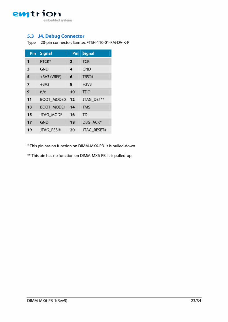
5.3 J4, Debug Connector Type 20-pin connector, Samtec FTSH-110-01-FM-DV-K-P
Pin Signal Pin Signal
1 RTCK* 2 TCK
3 GND 4 GND
5 +3V3 (VREF) 6 TRST#
7 +3V3 8 +3V3
9 n/c 10 TDO
11 BOOT_MODE0 12 JTAG_DE#**
13 BOOT_MODE1 14 TMS
15 JTAG_MODE 16 TDI
17 GND 18 DBG_ACK*
19 JTAG_RESI# 20 JTAG_RESET#
* This pin has no function on DIMM-MX6-PB. It is pulled-down.
** This pin has no function on DIMM-MX6-PB. It is pulled-up.
DIMM-MX6-PB-1 (Rev5) 24/34
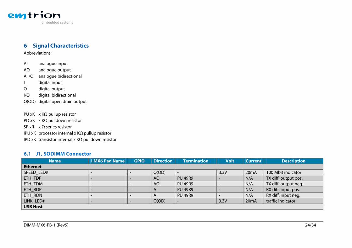
6 Signal Characteristics Abbreviations:
AI analogue input
AO analogue output
A I/O analogue bidirectional
I digital input
O digital output
I/O digital bidirectional
O(OD) digital open drain output
PU xK x KΩ pullup resistor
PD xK x KΩ pulldown resistor
SR xR x Ω series resistor
IPU xK processor internal x KΩ pullup resistor
IPD xK transistor internal x KΩ pulldown resistor
6.1 J1, SODIMM Connector
Name i.MX6 Pad Name GPIO Direction Termination Volt Current Description Ethernet SPEED_LED# - - O(OD) - 3.3V 20mA 100 Mbit indicator
ETH_TDP - - AO PU 49R9 - N/A TX diff. output pos. ETH_TDM - - AO PU 49R9 - N/A TX diff. output neg. ETH_RDP - - AI PU 49R9 - N/A RX diff. input pos. ETH_RDN - - AI PU 49R9 - N/A RX diff. input neg. LINK_LED# - - O(OD) - 3.3V 20mA traffic indicator USB Host
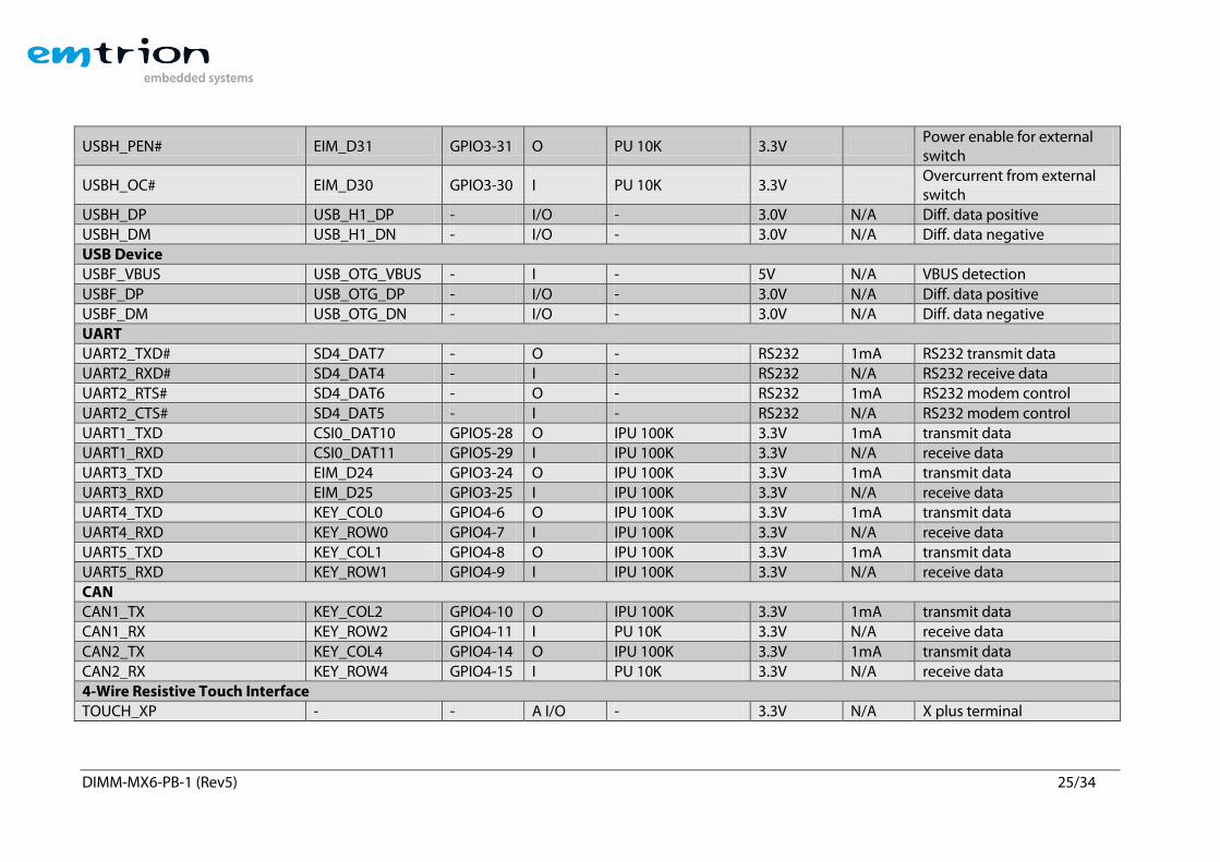
DIMM-MX6-PB-1 (Rev5) 25/34
USBH_PEN# EIM_D31 GPIO3-31 O PU 10K 3.3V Power enable for external switch
USBH_OC# EIM_D30 GPIO3-30 I PU 10K 3.3V Overcurrent from external switch
USBH_DP USB_H1_DP - I/O - 3.0V N/A Diff. data positive USBH_DM USB_H1_DN - I/O - 3.0V N/A Diff. data negative USB Device USBF_VBUS USB_OTG_VBUS - I - 5V N/A VBUS detection
USBF_DP USB_OTG_DP - I/O - 3.0V N/A Diff. data positive USBF_DM USB_OTG_DN - I/O - 3.0V N/A Diff. data negative UART UART2_TXD# SD4_DAT7 - O - RS232 1mA RS232 transmit data UART2_RXD# SD4_DAT4 - I - RS232 N/A RS232 receive data UART2_RTS# SD4_DAT6 - O - RS232 1mA RS232 modem control UART2_CTS# SD4_DAT5 - I - RS232 N/A RS232 modem control UART1_TXD CSI0_DAT10 GPIO5-28 O IPU 100K 3.3V 1mA transmit data UART1_RXD CSI0_DAT11 GPIO5-29 I IPU 100K 3.3V N/A receive data UART3_TXD EIM_D24 GPIO3-24 O IPU 100K 3.3V 1mA transmit data UART3_RXD EIM_D25 GPIO3-25 I IPU 100K 3.3V N/A receive data UART4_TXD KEY_COL0 GPIO4-6 O IPU 100K 3.3V 1mA transmit data UART4_RXD KEY_ROW0 GPIO4-7 I IPU 100K 3.3V N/A receive data UART5_TXD KEY_COL1 GPIO4-8 O IPU 100K 3.3V 1mA transmit data UART5_RXD KEY_ROW1 GPIO4-9 I IPU 100K 3.3V N/A receive data CAN CAN1_TX KEY_COL2 GPIO4-10 O IPU 100K 3.3V 1mA transmit data CAN1_RX KEY_ROW2 GPIO4-11 I PU 10K 3.3V N/A receive data
CAN2_TX KEY_COL4 GPIO4-14 O IPU 100K 3.3V 1mA transmit data CAN2_RX KEY_ROW4 GPIO4-15 I PU 10K 3.3V N/A receive data 4-Wire Resistive Touch Interface TOUCH_XP - - A I/O - 3.3V N/A X plus terminal
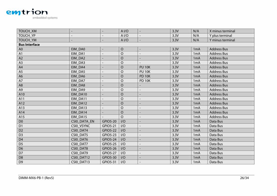
DIMM-MX6-PB-1 (Rev5) 26/34
TOUCH_XM - - A I/O - 3.3V N/A X minus terminal TOUCH_YP - - A I/O - 3.3V N/A Y plus terminal TOUCH_YM - - A I/O - 3.3V N/A Y minus terminal Bus Interface A0 EIM_DA0 - O - 3.3V 1mA Address Bus A1 EIM_DA1 - O - 3.3V 1mA Address Bus A2 EIM_DA2 - O - 3.3V 1mA Address Bus A3 EIM_DA3 - O - 3.3V 1mA Address Bus A4 EIM_DA4 - O PU 10K 3.3V 1mA Address Bus A5 EIM_DA5 - O PU 10K 3.3V 1mA Address Bus A6 EIM_DA6 - O PD 10K 3.3V 1mA Address Bus A7 EIM_DA7 - O PD 10K 3.3V 1mA Address Bus A8 EIM_DA8 - O - 3.3V 1mA Address Bus A9 EIM_DA9 - O - 3.3V 1mA Address Bus A10 EIM_DA10 - O - 3.3V 1mA Address Bus A11 EIM_DA11 - O - 3.3V 1mA Address Bus A12 EIM_DA12 - O - 3.3V 1mA Address Bus A13 EIM_DA13 - O - 3.3V 1mA Address Bus A14 EIM_DA14 - O - 3.3V 1mA Address Bus A15 EIM_DA15 - O - 3.3V 1mA Address Bus D0 CSI0_DATA_EN GPIO5-20 I/O - 3.3V 1mA Data Bus D1 CSI0_VSYNC GPIO5-21 I/O - 3.3V 1mA Data Bus D2 CSI0_DAT4 GPIO5-22 I/O - 3.3V 1mA Data Bus D3 CSI0_DAT5 GPIO5-23 I/O - 3.3V 1mA Data Bus
D4 CSI0_DAT6 GPIO5-24 I/O - 3.3V 1mA Data Bus D5 CSI0_DAT7 GPIO5-25 I/O - 3.3V 1mA Data Bus D6 CSI0_DAT8 GPIO5-26 I/O - 3.3V 1mA Data Bus D7 CSI0_DAT9 GPIO5-27 I/O - 3.3V 1mA Data Bus D8 CSI0_DAT12 GPIO5-30 I/O - 3.3V 1mA Data Bus D9 CSI0_DAT13 GPIO5-31 I/O - 3.3V 1mA Data Bus
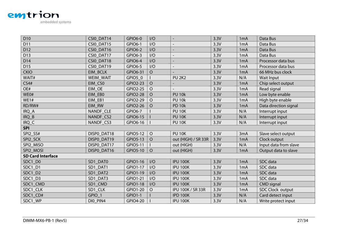
DIMM-MX6-PB-1 (Rev5) 27/34
D10 CSI0_DAT14 GPIO6-0 I/O - 3.3V 1mA Data Bus D11 CSI0_DAT15 GPIO6-1 I/O - 3.3V 1mA Data Bus D12 CSI0_DAT16 GPIO6-2 I/O - 3.3V 1mA Data Bus D13 CSI0_DAT17 GPIO6-3 I/O - 3.3V 1mA Data Bus D14 CSI0_DAT18 GPIO6-4 I/O - 3.3V 1mA Processor data bus D15 CSI0_DAT19 GPIO6-5 I/O - 3.3V 1mA Processor data bus CKIO EIM_BCLK GPIO6-31 O - 3.3V 1mA 66 MHz bus clock WAIT# WEIM_WAIT GPIO5_0 I PU 2K2 3.3V N/A Wait Input CS4# EIM_CS0 GPIO2-23 O - 3.3V 1mA Chip select output OE# EIM_OE GPIO2-25 O - 3.3V 1mA Read signal WE0# EIM_EB0 GPIO2-28 O PU 10k 3.3V 1mA Low byte enable WE1# EIM_EB1 GPIO2-29 O PU 10k 3.3V 1mA High byte enable RD/RW# EIM_RW GPIO2-26 O PD 10k 3.3V 1mA Data direction signal IRQ_A NANDF_CLE GPIO6-7 I PU 10K 3.3V N/A Interrupt input IRQ_B NANDF_CS2 GPIO6-15 I PU 10K 3.3V N/A Interrupt input IRQ_C NANDF_CS3 GPIO6-16 I PU 10K 3.3V N/A Interrupt input SPI SPI2_SS# DISP0_DAT18 GPIO5-12 O PU 10K 3.3V 3mA Slave select output SPI2_SCK DISP0_DAT19 GPIO5-13 O out (HIGH) / SR 33R 3.3V 1mA Clock output SPI2_MISO DISP0_DAT17 GPIO5-11 I out (HIGH) 3.3V N/A Input data from slave SPI2_MOSI DISP0_DAT16 GPIO5-10 O out (HIGH) 3.3V 1mA Output data to slave SD Card Interface SDC1_D0 SD1_DAT0 GPIO1-16 I/O IPU 100K 3.3V 1mA SDC data SDC1_D1 SD1_DAT1 GPIO1-17 I/O IPU 100K 3.3V 1mA SDC data
SDC1_D2 SD1_DAT2 GPIO1-19 I/O IPU 100K 3.3V 1mA SDC data SDC1_D3 SD1_DAT3 GPIO1-21 I/O IPU 100K 3.3V 1mA SDC data SDC1_CMD SD1_CMD GPIO1-18 I/O IPU 100K 3.3V 1mA CMD signal SDC1_CLK SD1_CLK GPIO1-20 O IPU 100K / SR 33R 3.3V 1mA SDC Clock output SDC1_CD# GPIO_1 GPIO1-1 I IPD 100K 3.3V N/A Card detect input SDC1_WP DI0_PIN4 GPIO4-20 I IPU 100K 3.3V N/A Write protect input
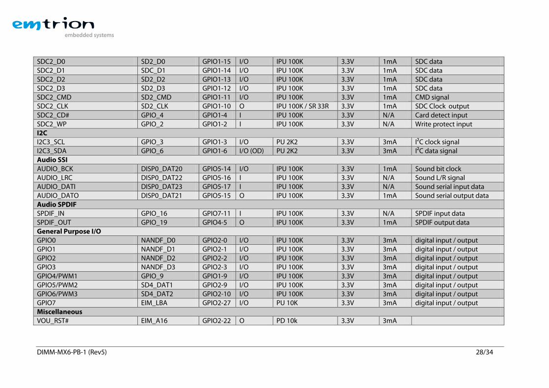
DIMM-MX6-PB-1 (Rev5) 28/34
SDC2_D0 SD2_D0 GPIO1-15 I/O IPU 100K 3.3V 1mA SDC data SDC2_D1 SDC_D1 GPIO1-14 I/O IPU 100K 3.3V 1mA SDC data SDC2_D2 SD2_D2 GPIO1-13 I/O IPU 100K 3.3V 1mA SDC data SDC2_D3 SD2_D3 GPIO1-12 I/O IPU 100K 3.3V 1mA SDC data SDC2_CMD SD2_CMD GPIO1-11 I/O IPU 100K 3.3V 1mA CMD signal SDC2_CLK SD2_CLK GPIO1-10 O IPU 100K / SR 33R 3.3V 1mA SDC Clock output SDC2_CD# GPIO_4 GPIO1-4 I IPU 100K 3.3V N/A Card detect input SDC2_WP GPIO_2 GPIO1-2 I IPU 100K 3.3V N/A Write protect input I2C I2C3_SCL GPIO_3 GPIO1-3 I/O PU 2K2 3.3V 3mA I²C clock signal I2C3_SDA GPIO_6 GPIO1-6 I/O (OD) PU 2K2 3.3V 3mA I²C data signal Audio SSI AUDIO_BCK DISP0_DAT20 GPIO5-14 I/O IPU 100K 3.3V 1mA Sound bit clock AUDIO_LRC DISP0_DAT22 GPIO5-16 I IPU 100K 3.3V N/A Sound L/R signal AUDIO_DATI DISP0_DAT23 GPIO5-17 I IPU 100K 3.3V N/A Sound serial input data AUDIO_DATO DISP0_DAT21 GPIO5-15 O IPU 100K 3.3V 1mA Sound serial output data Audio SPDIF SPDIF_IN GPIO_16 GPIO7-11 I IPU 100K 3.3V N/A SPDIF input data SPDIF_OUT GPIO_19 GPIO4-5 O IPU 100K 3.3V 1mA SPDIF output data General Purpose I/O GPIO0 NANDF_D0 GPIO2-0 I/O IPU 100K 3.3V 3mA digital input / output GPIO1 NANDF_D1 GPIO2-1 I/O IPU 100K 3.3V 3mA digital input / output GPIO2 NANDF_D2 GPIO2-2 I/O IPU 100K 3.3V 3mA digital input / output GPIO3 NANDF_D3 GPIO2-3 I/O IPU 100K 3.3V 3mA digital input / output
GPIO4/PWM1 GPIO_9 GPIO1-9 I/O IPU 100K 3.3V 3mA digital input / output GPIO5/PWM2 SD4_DAT1 GPIO2-9 I/O IPU 100K 3.3V 3mA digital input / output GPIO6/PWM3 SD4_DAT2 GPIO2-10 I/O IPU 100K 3.3V 3mA digital input / output GPIO7 EIM_LBA GPIO2-27 I/O PU 10K 3.3V 3mA digital input / output Miscellaneous VOU_RST# EIM_A16 GPIO2-22 O PD 10k 3.3V 3mA
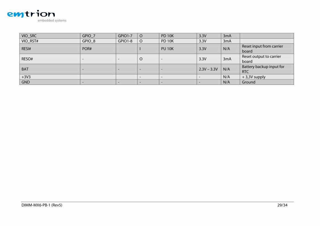
DIMM-MX6-PB-1 (Rev5) 29/34
VIO_SRC GPIO_7 GPIO1-7 O PD 10K 3.3V 3mA VIO_RST# GPIO_8 GPIO1-8 O PD 10K 3.3V 3mA
RESI# POR# I PU 10K 3.3V N/A Reset input from carrier board
RESO# - - O - 3.3V 3mA Reset output to carrier board
BAT - - - - 2.3V – 3.3V N/A Battery backup input for RTC
+3V3 - - - N/A + 3,3V supply GND - - - - - N/A Ground
DIMM-MX6-PB-1 (Rev5) 30/34
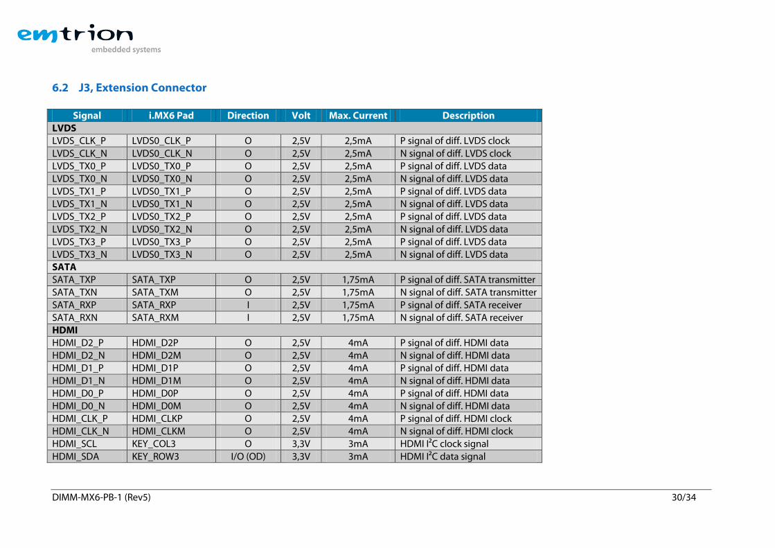
6.2 J3, Extension Connector
Signal i.MX6 Pad Direction Volt Max. Current Description LVDS LVDS_CLK_P LVDS0_CLK_P O 2,5V 2,5mA P signal of diff. LVDS clock LVDS_CLK_N LVDS0_CLK_N O 2,5V 2,5mA N signal of diff. LVDS clock LVDS_TX0_P LVDS0_TX0_P O 2,5V 2,5mA P signal of diff. LVDS data LVDS_TX0_N LVDS0_TX0_N O 2,5V 2,5mA N signal of diff. LVDS data LVDS_TX1_P LVDS0_TX1_P O 2,5V 2,5mA P signal of diff. LVDS data LVDS_TX1_N LVDS0_TX1_N O 2,5V 2,5mA N signal of diff. LVDS data LVDS_TX2_P LVDS0_TX2_P O 2,5V 2,5mA P signal of diff. LVDS data
LVDS_TX2_N LVDS0_TX2_N O 2,5V 2,5mA N signal of diff. LVDS data LVDS_TX3_P LVDS0_TX3_P O 2,5V 2,5mA P signal of diff. LVDS data LVDS_TX3_N LVDS0_TX3_N O 2,5V 2,5mA N signal of diff. LVDS data SATA SATA_TXP SATA_TXP O 2,5V 1,75mA P signal of diff. SATA transmitter SATA_TXN SATA_TXM O 2,5V 1,75mA N signal of diff. SATA transmitter
SATA_RXP SATA_RXP I 2,5V 1,75mA P signal of diff. SATA receiver SATA_RXN SATA_RXM I 2,5V 1,75mA N signal of diff. SATA receiver HDMI HDMI_D2_P HDMI_D2P O 2,5V 4mA P signal of diff. HDMI data HDMI_D2_N HDMI_D2M O 2,5V 4mA N signal of diff. HDMI data HDMI_D1_P HDMI_D1P O 2,5V 4mA P signal of diff. HDMI data HDMI_D1_N HDMI_D1M O 2,5V 4mA N signal of diff. HDMI data HDMI_D0_P HDMI_D0P O 2,5V 4mA P signal of diff. HDMI data HDMI_D0_N HDMI_D0M O 2,5V 4mA N signal of diff. HDMI data HDMI_CLK_P HDMI_CLKP O 2,5V 4mA P signal of diff. HDMI clock HDMI_CLK_N HDMI_CLKM O 2,5V 4mA N signal of diff. HDMI clock HDMI_SCL KEY_COL3 O 3,3V 3mA HDMI I²C clock signal HDMI_SDA KEY_ROW3 I/O (OD) 3,3V 3mA HDMI I²C data signal
DIMM-MX6-PB-1 (Rev5) 31/34
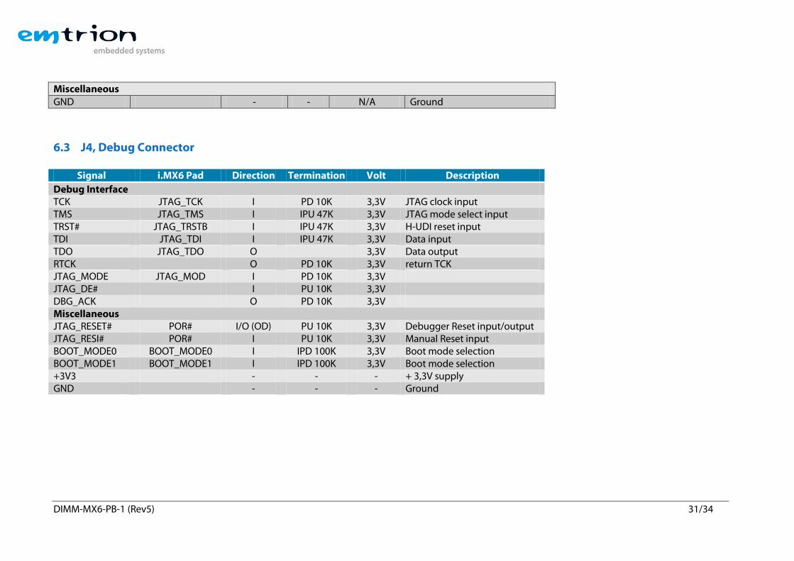
Miscellaneous GND - - N/A Ground
6.3 J4, Debug Connector
Signal i.MX6 Pad Direction Termination Volt Description
Debug Interface TCK JTAG_TCK I PD 10K 3,3V JTAG clock input TMS JTAG_TMS I IPU 47K 3,3V JTAG mode select input TRST# JTAG_TRSTB I IPU 47K 3,3V H-UDI reset input TDI JTAG_TDI I IPU 47K 3,3V Data input TDO JTAG_TDO O 3,3V Data output RTCK O PD 10K 3,3V return TCK JTAG_MODE JTAG_MOD I PD 10K 3,3V JTAG_DE# I PU 10K 3,3V DBG_ACK O PD 10K 3,3V Miscellaneous JTAG_RESET# POR# I/O (OD) PU 10K 3,3V Debugger Reset input/output JTAG_RESI# POR# I PU 10K 3,3V Manual Reset input BOOT_MODE0 BOOT_MODE0 I IPD 100K 3,3V Boot mode selection BOOT_MODE1 BOOT_MODE1 I IPD 100K 3,3V Boot mode selection +3V3 - - - + 3,3V supply GND - - - Ground
DIMM-MX6-PB-1 (Rev5) 32/34
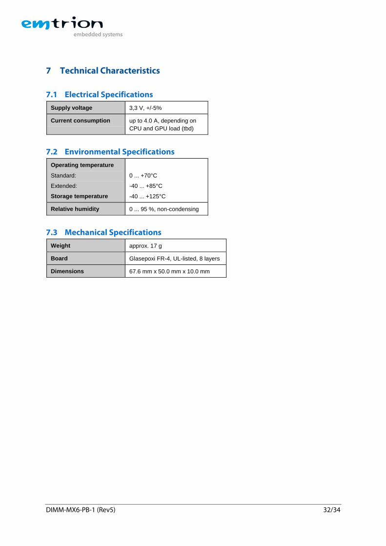
7 Technical Characteristics
7.1 Electrical Specifications
Supply voltage 3,3 V, +/-5%
Current consumption up to 4.0 A, depending on
CPU and GPU load (tbd)
7.2 Environmental Specifications
Operating temperature
Standard:
Extended:
Storage temperature
0 ... +70°C
-40 ... +85°C
-40 ... +125°C
Relative humidity 0 ... 95 %, non-condensing
7.3 Mechanical Specifications
Weight approx. 17 g
Board Glasepoxi FR-4, UL-listed, 8 layers
Dimensions 67.6 mm x 50.0 mm x 10.0 mm
DIMM-MX6-PB-1 (Rev5) 33/34
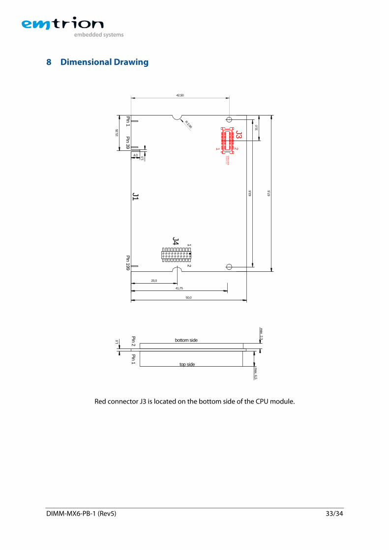
8 Dimensional Drawing
11,0
67,6
63,6
20,0
50,0
1,0
4,0
15,3
5
Pin
1P
in 3
9P
in 1
99
1,0
max. 6
,5
max. 2
,3
Pin
1P
in 2 bottom side
top side
41,75
J1
J4
J3
42,50
12
R 2,00
1 2
529910308
Recepta
cle
Core
Red connector J3 is located on the bottom side of the CPU module.
DIMM-MX6-PB-1 (Rev5) 34/34
9 References [1] i.MX6x
Reference Manual i.MX 6Dual/6Quad Applications Processor Reference Manual IMX6DQRM Rev. 3, 07/2015 Freescale
[2] i.MX6x Datasheet i.MX 6Dual/6Quad Applications Processors for Industrial Products IMX6DQIEC Rev. 4, 07/2015 Freescale
[3] AR1020 Datasheet AR1000 Series Resistive Touch Screen Controller DS41393A Microchip Technology Inc.