Embed Size (px)
Citation preview

Page [1]
Enrollment No……………………….
Diploma in Engineering (Polytechnic)
Third Semester Main Examination, Dec-2020
Electronic Components and Materials [ECD301]
Branch-ETC
Time: 3:00 Hrs Max Marks 70
Note : Student should not write anything on question paper.
Question no. 1 is compulsory. Attempt any five questions from Q.2 to Q.8
Q.1 Multiple Choice Question / oLrqfu"B iz’u [2×5=10]
(i) The instrument which may be used to measure the optical activity of compounds
is - वह उपकरण जिसका उपयोग यौजगको की ऑजटिकल गजिजवजि को मापन क जलए जकया िा सकिा ह -
(a) Infrared spectrometer / इनफरारड सपकटरोमीिर
(b) Atomic absorption spectrometer / परमाण अवशोषण सपकटरोमीिर
(c) Polarimeter / पोलारीमीिर
(d) Fluoroscope / परजिदीजिदशी
(ii) The excitation of outer electrons in atoms and molecules is associated with
which of the following bands of radiation - परमाणओ और अणओ म बाहरी इलकटरॉनो का उततिना जवजकरण क जनमनजलजिि बडो म स जकसक साथ िडा हआ ह -
(a) X-rays / एकटस-र (b) Gamma rays /गामा जकरण
(c) Ultra violet /अलटरा वायलि (d) Infrared /इनफरारड
(iii) Which of the following is a polymer - / जनमन म स कौन सा एक बहलक ह
(a) Plastic / टलाजसिक (b) Glycogen / गलाइकोिन
(c) Starch / सिारच (d) All of these / य सब
(iv) Ultra violet radiation is emitted when electron jumps from an outer stationary
orbit to - अलटरा वायलि जवजकरण उतसजिचि होिा ह िब इलकटरॉन एक बाहरी जसथर ककषा स कदिा ह -
(a) First stationary orbit / परथम जसथर ककषा
(b) Second stationary orbit / दसरी जसथर ककषा
(c) Third stationary orbit / िीसरा जसथर ककषा
(d) Fourth stationary orbit / रौथा जसथर ककषा
Page [2]
(v) Polarization is a measure of - / धरवीकरण का एक उपाय ह -
(a) Dielectric constant per unit volume / ढाकिा हआ जनरिर परजि इकाई आयिन
(b) Voltage gradient to produce electrical breakout / जवदयि बरकआउि का उतपादन करन क
जलए वोलटिि ढाल
(c) Product of charge and distance / परभारी और दरी क उतपाद
(d) Excess charge density / अतयजिक रािच घनतव
Q.2 (a) Explain energy band diagram of conductor, insulator and semiconductor? कडकटिर, इनफसलिर और अिचरालक क ऊिाच बड आरि की वयाखया कर ।
(b) Difference between conductor and semiconductor based on atomic
structure? परमाण सररना पर आिाररि कडकटिर और अिचरालक क बीर अिर बिाओ l
Q.3 (a) Explain different types of fuses and its application? जवजभनफन परकार क फयज और उसक आवदन की वयाखया कर ।
(b) Explain p-n junction diode characteristics? पी-एन िकटशन डायोड जवशषिाओ की वयाखया कर?
Q.4 (a) Explain the properties of magnetic materials? रबकीय सामगरी क गणो की वयाखया कर?
(b) Write short note on hard and soft magnetic materials. हाडच और मलायम रबकीय सामगरी पर सजकषि नोि जलि ।
Q.5 (a) Explain B-H curve and hysteresis effect. बी-एर वकर और जहसरजसस परभाव समझाओ ।
(b) Explain diamagnetic, paramagnetic and ferromagnetic materials. हीरगनजिक, परामगनजिक और फरोमगनजिक सामगरी समझाए ।
Q.6 (a) Explain jointing technique, screw jointing and soldering. सयकत िकनीक, सकर सयकतकरण और सोलटडररग समझाओ ।
(b) Write down types of solders. सोलटडर क परकार जलि ।
Q.7 (a) Explain Soldering process. सोलटडररग परजकरया की वयाखया कर ।
(b) Explain different soldering materials used in electronics. Explain all
soldering Materials. इलकटरॉजनकटस म इसिमाल जवजभनफन सोलटडररग सामगरी की वयाखया कर । सभी सोलटडररग समझा सामगरी ।
Q.8 (a) Explain concept of ideal voltage and current source. आदशच वोलटिि और िारा सरोि की अविारणा की वयाखया कर ।
(b) Explain primary and secondary cells. पराथजमक और माधयजमक कोजशकाओ की वयाखया कर ।

Page [1]
Enrollment No……………………….
Diploma in Engineering (Polytechnic)
Third Semester Main Examination, Dec-2020
Electronic Devices and Circuits [ECD302]
Branch-ETC
Time: 3:00 Hrs Max Marks 70 Note : Student should not write anything on question paper.
Question no. 1 is compulsory. Attempt any five questions from Q.2 to Q.9
Q.1 Multiple choice Question / oLrqfu"B iz’u [2x5=10]
(i) ____ number of terminals does a diode have-
____VfeZuyksa dh la[;k ,d Mk;ksM gS &
(a) 1 / ,d (b) 2 / nks
(c) 3 / rhu (d) 4 / pkj
(ii) Which of the following option defines the diode- fuEufyf[kr esa ls dkSu lk fodYi Mk;ksM dks ifjHkkf"kr djrk gS&
(a) Is the simplest of semiconductor devices / v/kZpkyd midj.kksa esa lcls ljy gS
(b) Has characteristics that closely match those of a simple switch / ,slh fo'ks"krk,a gSa tks ,d lk/kkj.k fLop ds lkFk esy [kkrh gSa
(c) Is a two terminal device / ,d nks VfeZuy fMokbl gS
(d) All the above / mijksä lHkh
(iii) Which of the following elements are most frequently used for doping pure Ge or Si-
fuEufyf[kr esa ls dkSu lk rRo Mksfiax 'kq) Ge ;k Si ds fy, lcls vf/kd ckj mi;ksx fd;k
tkrk gS&
(a) Boron / cksju (b) Gallium / xSfy;e
(c) Indium / bf.M;e (d) All the above / mijksä lHkh
(iv) In which of the following state does the silicon diode has the voltage drop of 0.7V-
fuEufyf[kr esa ls fdl voLFkk esa flfyd‚u Mk;ksM esa 0-7V dk oksYVst Mª‚i gS&
(a) No bias / dksbZ iwokZxzg ugha (b) Forward Bias / Q‚joMZ ck;l
(c) Reverse Bias / fjolZ ck;l (d) Zener region / tsuj {ks=
(v) One ev is equal to __________
,d ev __________ ds cjkcj gS&
(a) 6.02 × 10²³ (b) 1.6 × 10
-19
(c) 6.25 × 10¹⁸ (d) 1.66 × 10
-24

Page [2]
Q.2 (a) Draw and Explain the VI Characteristic of a PN Junction Diode.
ih,u taD'ku Mk;ksM dh VI fo'ks"krk dks Mªk djs vkSj le>kb,\
(b) Draw the VI characteristic of Zener diode and explain its operation.
tsuj Mk;ksM dh VI fo'ks"krk Mªk djs vkSj blds lapkyu dh O;k[;k dhft,A
Q.3 (a) What is varactor diode? Explain it.
oSjk,DVj Mk;ksM D;k gS\ bls le>kb,A
(b) Explain the basic structure and working of light emitting diode.
ykbV ,fefVax Mk;ksM ds cqfu;knh <kaps vkSj dkedkt dh O;k[;k dhft,A
Q.4 (a) Difference between clippers and clampers.
fDyijl vkSj DySailZ ds chp varj crkb,A
(b) Explain half wave rectifier and Full wave rectifier.
vk/ks rjax lq/kkjd vkSj iw.kZ ygj lq/kkjd dks le>kb,A
Q.5 (a) Show that PN diode work as a rectifier.
fn[kk,a fd ih,u Mk;ksM ,d jsDVhQk;j ds :i esa dSls dke djrk gS\
(b) Explain filter circuit and types of filters.
fQYVj lfdZV vkSj fQYVj ds çdkj le>kb,A
Q.6 (a) Write down the operation of NPN transistor with schematic diagram.
;kstukc) vkjs[k ds lkFk ,uih,u VªkaftLVj ds lapkyu dks fyf[k,A
(b) Write down the transistor configuration CE and CB mode with schematic
Diagram.
;kstukc) vkjs[k ds lkFk VªkaftLVj foU;kl lhbZ vkSj lhch eksM fyf[k,A
Q.7 (a) Define α and β of BJT.
chtsVh ds β vkSj ∝ ifjHkkf"kr dhft,A
(b) Describe the working of Depletion type MOSFET.
fMyh'ku çdkj MOSFET ds dkedkt dk o.kZu dhft,A
Q.8 (a) Explain CE amplifier
lhbZ ,EiyhQk;j le>kb,A
(b) Write short note on class A Amplifier, Class B Amplifier and Class C Amplifier. d{kk , ,EiyhQk;j] d{kk ch ,EiyhQk;j vkSj d{kk lh ,EiyhQk;j ij laf{kIr uksV fyf[k,A
Q.9 (a) Explain frequency distortion and phase shift distortion.
vko`fÙk fo:i.k vkSj pj.k f'k¶V fo:i.k le>kb,A
(b) Explain and sketch block diagram of feedback amplifier.
QhMcSd ,EiyhQk;j ds Cy‚d vkjs[k dh O;k[;k vkSj Ldsp dhft,A

Page [1]
Enrollment No……………………….
Diploma in Engineering (Polytechnic)
Third Semester Main Examination, Dec-2020
Basic Electrical Engineering [ECD303]
Branch-ETC
Time: 3:00 Hrs Max Marks 70
Note : Student should not write anything on question paper.
Question no. 1 is compulsory. Attempt any five questions from Q.2 to Q.9
Q.1 Multiple Choice Question / oLrqfu"B iz'u [2×5=10]
(i) The cut & in voltage for silicon and germanium are- dV bZu flfyd‚u vkSj tesZfu;e ds fy, oksYVst D;k gS&
(a) 0-3 V / 0-3 oh (b) 0-3 V/ 0-7 oh
(c) 0-7 V/ 0-7 oh
(d) 0-7 V / 0-3 oh
(ii) The P type semiconductor impurities are also called as ih çdkj v/kZpkyd esa v'kqf);ksa dks D;k dgk tkrk gS&
(a) Acceptor impurities/v'kqf);ksa dks Lohdkj djusokyk
(b) Donor impurities/ nkrk v'kqf);k¡
(c) Either (a) or (b) / ;k rks ,d ;k ch
(d) None of these/ buesa ls dksbZ ugh
(iii) In N type semiconductor, the impurities added to a semiconductor are- ,u Vkbi lsehdaMDVj esa v'kqf);ksa dks D;k dgk tkrk gS&
(a) Trivalent / VkbosysUV (b) Pentavalent/ isUVkosysUV
(c) Monovalent/ eksuksosysUV (d) Tetravalent/ VsVªkosysUV
(iv) Impurities are generally added in the pure semiconductor to- v'kqf);ksa dks vke rkSj ij 'kq) v/kZpkyd esa tksM+k tkrk gS&
(a) Increase the number of electrons/ bysDVª‚uksa dh la[;k esa o`f)
(b) Increase the number of holes/ gksYl dh la[;k esa of)
(c) Increase their conductivity / pkydrk esa of)
(d) All of these / ;s lHkh
(v) In DOL fuses are provided to protect against Mhvks,y ¶;wt esa lqj{kk ds fy, çnku fd;k tkrk gS
(a) Short circuit protection/ 'k‚VZ lfdZV lqj{kk
(b) Over voltage/ oksYVst ls vf/kd
(c) Over current/ orZeku ij
(d) Over load / vksoj yksM
Page [2]
Q.2 (a) What is source? Explain Ideal current source and voltage source. lzksr D;k gS \ vkn'kZ orZeku lzksr vkSj oksYVst lzksr le>kb, A
(b) State and explain Ohm’s Law. vkse dk fu;e fy[ks vkSj le>kb,A
Q.3 (a) What is resistance? Explain series and parallel connection of resistance. çfrjks/k D;k gS\ çfrjks/k dh Ja[kyk vkSj lekukarj dusD'ku dh O;k[;k dhft,A
(b) Explain statement of KCL and KVL.
KCL vkSj KVL ds dFku le>kb,A
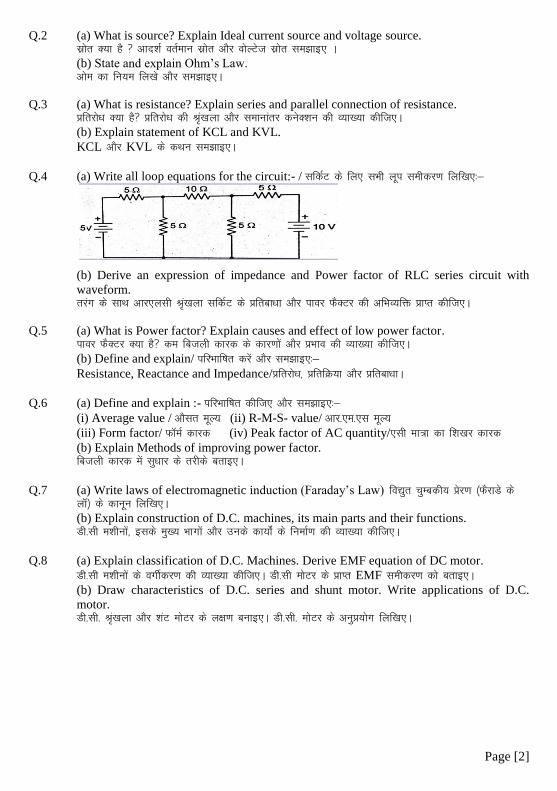
Q.4 (a) Write all loop equations for the circuit:- / lfdZV ds fy, lHkh ywi lehdj.k fyf[k,%&
(b) Derive an expression of impedance and Power factor of RLC series circuit with
waveform. rjax ds lkFk vkj,ylh J`a[kyk lfdZV ds çfrck/kk vkSj ikoj QSDVj dh vfHkO;fä çkIr dhft,A
Q.5 (a) What is Power factor? Explain causes and effect of low power factor. ikoj QSDVj D;k gS\ de fctyh dkjd ds dkj.kksa vkSj çHkko dh O;k[;k dhft,A
(b) Define and explain/ ifjHkkf"kr djsa vkSj le>kb,%&
Resistance, Reactance and Impedance/çfrjks/k] çfrfØ;k vkSj çfrck/kkA
Q.6 (a) Define and explain :- ifjHkkf"kr dhft, vkSj le>kb,%&
(i) Average value / vkSlr ewY; (ii) R-M-S- value/ vkj-,e-,l ewY;
(iii) Form factor/ Q‚eZ dkjd (iv) Peak factor of AC quantity/,lh ek=k dk f'k[kj dkjd
(b) Explain Methods of improving power factor. fctyh dkjd esa lq/kkj ds rjhds crkb,A
Q.7 (a) Write laws of electromagnetic induction (Faraday’s Law) fo|qr pqEcdh; çsj.k ¼QSjkMs ds
ykW½ ds dkuwu fyf[k,A
(b) Explain construction of D.C. machines, its main parts and their functions. Mh-lh e'khuksa] blds eq[; Hkkxksa vkSj muds dk;ksaZ ds fuekZ.k dh O;k[;k dhft,A
Q.8 (a) Explain classification of D.C. Machines. Derive EMF equation of DC motor.
Mh-lh e'khuksa ds oxhZdj.k dh O;k[;k dhft,A Mh-lh eksVj ds çkIr EMF lehdj.k dks crkb,A
(b) Draw characteristics of D.C. series and shunt motor. Write applications of D.C.
motor. Mh-lh- Ja[kyk vkSj 'kaV eksVj ds y{k.k cukb,A Mh-lh- eksVj ds vuqç;ksx fyf[k,A

Page [1]
Enrollment No……………………….
Diploma in Engineering (Polytechnic)
Third Semester Main Examination, Dec-2020
Network Analysis [ECD304]
Branch-ETC
Time: 3:00 Hrs Max Marks 70 Note : Student should not write anything on question paper.
Question No. 1 is compulsory. Attempt any five questions from Q.2 to Q.9
Q.1 Multiple Choice Question / oLrqfu"B iz'u [2×5=10]
(i) An RLC series circuit is under damped the value of R ,d vkj-,y-lh Ja[kyk lfdV Hkhx jgk gSA bls ue cukus ds fy, vkj dk ewY;
(a) Has to be increased / c<kuk gksxk
(b) Has to be decreased / de fd;k tkuk gS
(c) Has to be increased to infinity / vuar rd c<k;k tkuk gSA
(d) Has to be reduced to zero / 'kwU; rd de fd;k tkuk gSA
(ii) Henry is equivalent to - gsujh ds led{k &
(a) Volts / Ampere / oksYV ,fEi;j
(b) Weber / Volt / oscj@oksYV
(c) Weber / Ampere/ oscj@ ,fEi;j
(d) Weber / Ampere2 / oscj@ Ampere
2
(iii) In a minimum function- U;wure dk;Z esa&
(a) The degree of numerator and denominator are equal /va'k vkSj gj dh la[;k cjkcj
gksrh gSA
(b) The degree of numerator and denominator are unequl/va'k vkSj gj dh fMxzh vlelu
gksrh gS
(c) The degree of numerator is one more than degree of / vaa'k dh fMxzh gj dh fMxzh ls ,d
vf/kd gS
(d) The degree of numerator is one less than degree of denominator/ vaa'k dh fMxzh gj
dh fMxzh ls ,d de gS
(iv) For a transmission line open circuit and short circuit impedances are 20 Ω and 5 Ω-
Then characteristic impedance is
,d Vªkalfe'ku ykbu ds fy, vkiu lfdV vkSj 'kkV lfdV bEihMsal 20 Ω vkSj 5 Ω gSaA rc pfj=
izfrck/kk gS
(a) 100 Ω / 100 Ω (b) 50 Ω / 50 Ω
(c) 25 Ω / 25 Ω (d) 10 Ω / 10 Ω

Page [2]
(v) The drift velocity of electrons is bysDVªkWuks dk cgko osx gS
(a) Very small as compared to speed of light /izdk'k xkfr dh rqyuk es cgqr NksVk gS
(b) Equal to speed of light / izdk'k dh xjfr ds cjkcj
(c) Almost equal to speed light / izdk'k dh xkfr ds yxHkx cjkcj
(d) Half the speed of light / vk/kh izdk’k dh xfr
Q.2 (a) Distinguish between/ varj crkb,A
(i) Node and junction / uksM vkSj tD'ku
(ii) Active and passive elements/ lfdz; vkSj fuf"Ø; rRo
(iii) Loop and mesh/ ywi vkSj es"k
(b)State and explain superposition theorem using superposition theorem determine
the current in 5 Ω resistor of the network shown below. Lqijiksft’ku izse; crkvks vkSj le>kvks lqijiksft'ku izes; dk mi;ksx djds uhps fn[kk, x, usVodZ es
5 Ω izfrjks/k eas djaV fu/kkZfjr djsaA
Q.3 (a) State and explain Kirchhoff s current and voltage laws.
Kirchhoff ds djV vkSj oksYVst dkuwu crkvks vkSj le>kb,A
(b) Define following terms: fuEufyf[kr dks ifjHkkf"kr djsa &
i) Quality Factor or Q Factor / xq.koÙkk QSDVj ;k D;w QSDVj
ii) Series Resonance / Ja[kyk vuqukn
iii) Band Width / cSaMfoMFk
Q.4 (a) Explain R&L&C parallel circuit with its phasor diagram. Qstj Mk;xzke ds lkFk vkj&,y&lh lekarj lfdZV le>k,a
(b) Explain steady state response of RL circuit. vkj ,y lfdZV dh fLFkj fLFkkfr izfrfØ;k dh O;kk[;k djsA
Q.5 (a) Distinguish between transient response for RL Circuit and RC Circuit. vkj-,y lfdZV vkSj vkj-lh lfdZV ds fy, {kf.kd çfrfØ;k ds chp varj djsaA
(b) What do you understand by Filters? Define Band Pass and Band Elimination
Filter. vki fQYVj }kjk D;k le>rs gSa\ cSaM ikl vkSj cSaM mUewyu fQYVj ifjHkkf"kr djsa

Page [3]
Q.6 (a) Derive an expression for constank k for low pass filter.
Yks ikl fQYVj ds fy, k fy, ,d vfHkO;fr izkIr djsA
(b) Distinguish between varj crkvks &
(i) Low Pass filter and High Pass filter/ yks ikl fQYVj vkSj mPp ikl fQYVj
(ii) Elementary & Derived filter and Elementary Composite filter/ izkFkfed ,e O;qriUk
fQYVj vkSj izFkkfed lexz fQYVj
Q.7 (a) What is tow port network? Classify types of two port network . Vw iksVZ usVodZ D;k gS\ Vw iksVZ usVodZ ds izdkj dks oxhZd`r djsA
(b) Derive an expression for short circuit admittance parameters 'kkWVZ lfdZV ,MehVsUl iSjkehVj ds fy, ,d vfHkO;fä izkIr dhft,A
Q.8 (a) What is attenuator? Classify types of attenuator ,V~uq,Vj D;k gS\ ,Vuq,Vj ds izdkj oxhZdr djsaA
(b) What do you understand Laplace transform? ysiysl VªkalQkeZ }kjk vki D;k le>rs gS\
Q.9 (a) What are the applications of Laplace transform in RL and RC circuit? vkj-,y vkSj vkj lh lfdV es ysiysl VªklQkeZ ds iz;ksx D;k gS\
(b) Find the Nodal voltages and the current through 2 Ω resistance.
2 Ω izfrjks/k esa uksMy oksYVst vkSj djaV [kkstsA

Page [1]
Enrollment No……………………….
Diploma in Engineering (Polytechnic)
Third Semester Main Examination, Dec-2020
Digital Electronics [ECD305]
Branch-ETC
Time: 3:00 Hrs Max Marks 70
Note : Student should not write anything on question paper.
Question no. 1 is compulsory. Attempt any five questions from Q.2 to Q.9
Q.1 Multiple Choice Question / [2x5=10]
(i) Most Demultiplexers facilitate which type of conversion vf/kdka'k MheYVhIysDllZ fdl çdkj ds :ikarj.k dh lqfo/kk nsrs gSa
(a) Decimal-to-hexadecimal /Msfley&ls&gsDlkMsfley
(b) Single input, multiple outputs / ,dy buiqV] dbZ vkmViqV
(c) AC to DC/ AC ls DC
(d) Odd parity to Even parity /lerk ls fo"ke lerk
(ii) In 1 to 4 Demultiplexer, how many select lines are required- 1 ls 4 MheYVhIysDlj esa fdrus pqfuank ykbuksa dh vko’;drk gksrh gS&
(a) 2 (b) 3
(c) 4 (d) 5
(iii) In 1 to 4 multiplexer, if C1=1 &C2 =1, Then the output will be-
1 ls 4 eYVhIysDlj esa] ;fn C1=1 & C2 =1 gS rks vkmViqV ______ gksxk&
(a) Y0 (b) Y1/ okbZ 1
(c) Y2 (d) Y3 / okbZ 3
(iv) How many select lines are required for a 1 to 8 de multiplexer- 1 ls 8 MheYVhIysDlj ds fy, fdruh pqfuank ykbuksa dh vko’;drk gksrh gS&
(a) 2 (b) 3
(c) 4 (d) 5
(v) How many AND gates are required for a 1 to 8 multiplexer
1 ls 8 eYVhIysDlj ds fy, fdrus AND xsV vko’;d gS a &
(a) 2 (b) 6
(c) 8 (d) 5

Page [2]
Q.2 (a) Convert binary to octal - ckbujh dks vkWDVy esa cnysa&
i) (10001011)2 = ( )8
ii) (110001101)2= ( )8
iii) (1001001001)2 = ( )8
(b) Use 2's complement to perform M-N with the given binary numbers. fn, x, f}/kkjh la[;kvksa ds lkFk ,e&,u djus ds fy, 2 ds iwjd dk mi;ksx dhft,A
M = 10101001 N = 10001001
Q.3 (a) Given binary numbers convert them into gray code - fn, x, ckbujh uEcj mUgsa xzs dksM esa ifjofrZr dhft,&
(i) 0100111 (ii) 10010111 (iii) 101010101
(b) Given Binary numbers convert them into Excess-3 & BCD fn, x, ckbujh uacj mUgssa vfrfjDr&3 vkSj chlhMh esa ifjofrZr djrs gS&
(i) 0010 (ii) 0100 (iii) 0101
Q.4 (a) Explain all laws of Boolean algebra cwfy;u chtxf.kr ds lHkh dkuwuksa dh O;k[;k dhft,A
(b) Explain De-Morgan’s theorem with suitable diagram. mi;qDr vkjs[k ds lkFk Mh&e‚xZu ds çes; dks le>kb,A
Q.5 (a) Minimize following Boolean expression using Boolean identity. cqfy;u igpku dk mi;ksx djds fuEufyf[kr cwfy;u vfHkO;fDr dks de dhft, &
F(A,B,C) = A'B' + A'B + BC + AB'C'
(b) Simplification of the following Boolean expression using K-map.
K-map dk mi;ksx dj fuEufyf[kr cwfy;u vfHkO;fä dk ljyhdj.k dhft, &
Y=A'B'+A'B+A'B
Q.6 (a) Explain DTL and ECL. MhVh,y vkSj bZlh,y le>kb,A
(b) Differentiate between TTL, ECL and CMOS. VhVh,y] bZlh,y vkSj lh,evks,l ds chp varj Li"V dhft,A
Q.7 (a) Explain Familiarization of IC’s. vkbZlh ds ifjfpr O;k[;k dh O;k[;k dhft,A
(b) Write down the flip & flop. f¶yi&¶y‚i fyf[k,A
Q.8 (a) Explain Half adder and full adder with diagram. vkjs[k ds lkFk vk/kk ;kstd vkSj iw.kZ ;kstd le>kb,A
(b) Explain Encoder and Decoder. ,udksMj vkSj fMdksMj fyf[k,A
Q.9 (a) Explain MUX and DEMUX. ,e;w,Dl vkSj MsE;wDl le>kb,A
(b) Explain Synchronous and Asynchronous rqY;dkfyd vkSj vlhfer le>kb,A