Embed Size (px)
Citation preview
Direct Current Distribution Systems
for Residential Areas
Powered by Distributed Generation
By
Faizan Dastgeer
Submitted for the degree of
Doctor of Philosophy
At
School of Engineering & Science
Faculty of Health, Engineering & Science
Victoria University, Australia
December 2011
VICTORIA UNIVERSITY, AUSTRALIA
“I, Faizan Dastgeer, declare that the PhD thesis entitled ‘DC
Distribution Systems for Residential Areas Powered by Distributed
Generation’ is no more than 100,000 words in length including
quotes and exclusive of tables, figures, appendices, bibliography,
references and footnotes. This thesis contains no material that
has been submitted previously, in whole or in part, for the award
of any other academic degree or diploma. Except where otherwise
indicated, this thesis is my own work”.
Dated: December 2011
Signature
ii

Table of Contents
Table of Contents iii
List of Figures vi
List of Tables ix
List of Acronyms x
Abstract xi
Acknowledgement xiii
1 Introduction 1
1.1 Importance of Power Electronic Converters in a DC Distribution
System . . . . . . . . . . . . . . . . . . . . . . . . . . . . . . . . 3
1.2 Publications . . . . . . . . . . . . . . . . . . . . . . . . . . . . . 4
1.3 Original Work . . . . . . . . . . . . . . . . . . . . . . . . . . . . 5
1.4 Organization of this Thesis . . . . . . . . . . . . . . . . . . . . . 6
2 Literature Review 9
2.1 DC Power Distribution System . . . . . . . . . . . . . . . . . . 10
2.2 Distributed Generation and Microgrids . . . . . . . . . . . . . . 11
2.3 DC Distributed Power System and its
Stability Issue . . . . . . . . . . . . . . . . . . . . . . . . . . . . 14
2.4 Applications of DC Distributed Power
Systems . . . . . . . . . . . . . . . . . . . . . . . . . . . . . . . 17
2.4.1 The International Space Station . . . . . . . . . . . . . . 17
2.4.2 Shipboard Power Systems . . . . . . . . . . . . . . . . . 17
2.4.3 Advanced Automobiles . . . . . . . . . . . . . . . . . . . 18
2.5 Constant Power Loads . . . . . . . . . . . . . . . . . . . . . . . 19
2.6 Brief History of Research Efforts in the Field of DC DPS Stability 20
2.7 Phase Plane Analysis . . . . . . . . . . . . . . . . . . . . . . . . 26
iii
2.8 Synergetic Control . . . . . . . . . . . . . . . . . . . . . . . . . 30
2.9 Pulse Adjustment Control Technique . . . . . . . . . . . . . . . 32
2.10 Varying System Damping to Cancel Out Negative Resistance
Effects . . . . . . . . . . . . . . . . . . . . . . . . . . . . . . . . 34
3 DC Distribution versus AC Distribution 38
3.1 Distribution System Modeling . . . . . . . . . . . . . . . . . . . 39
3.1.1 AC Distribution System Model . . . . . . . . . . . . . . 41
3.1.2 DC Distribution System Model . . . . . . . . . . . . . . 42
3.2 Results . . . . . . . . . . . . . . . . . . . . . . . . . . . . . . . . 44
3.2.1 Comment on Results . . . . . . . . . . . . . . . . . . . . 45
3.3 Minimum Required Efficiency for Power Electronic Converters
in DC Distribution System . . . . . . . . . . . . . . . . . . . . . 46
3.3.1 Step 1 . . . . . . . . . . . . . . . . . . . . . . . . . . . . 46
3.3.2 Step 2 . . . . . . . . . . . . . . . . . . . . . . . . . . . . 48
3.4 Case Study . . . . . . . . . . . . . . . . . . . . . . . . . . . . . 51
3.5 Summary . . . . . . . . . . . . . . . . . . . . . . . . . . . . . . 52
4 Hybrid of Voltage and Current Mode Control Technique 53
4.1 A Non-Linear State Space System Model . . . . . . . . . . . . . 56
4.2 HVC Control Technique . . . . . . . . . . . . . . . . . . . . . . 58
4.2.1 HVC Control - Mathematical Proof . . . . . . . . . . . 59
4.2.2 Lower Limit of 𝐼𝐿−𝑃𝑒𝑎𝑘 . . . . . . . . . . . . . . . . . . . 62
4.2.3 Shifting between Voltage and Current Mode Controls . . 62
4.3 Implementation of Controller for HVC Control Technique . . . . 63
4.4 Circuit based Simulation of System of Buck Converter and CPL
with HVC Control . . . . . . . . . . . . . . . . . . . . . . . . . 66
4.5 A Closer Look on Switching Cycles of 𝑖𝐿 Wave . . . . . . . . . . 71
4.6 Summary . . . . . . . . . . . . . . . . . . . . . . . . . . . . . . 74
5 Power Transfer Portraits of the System 75
5.1 Similarity of System Oscillations with LC Oscillations . . . . . . 76
5.2 System Time Intervals . . . . . . . . . . . . . . . . . . . . . . . 80
5.3 Power Transfer Portrait - For Stable
System . . . . . . . . . . . . . . . . . . . . . . . . . . . . . . . . 83
5.3.1 Varying Phase Difference . . . . . . . . . . . . . . . . . . 85
5.4 An Insight Into System Stability . . . . . . . . . . . . . . . . . . 87
5.5 Summary . . . . . . . . . . . . . . . . . . . . . . . . . . . . . . 92
6 Mathematical Expressions Related to HVC Control 93
6.1 An Expression for Upper Peak of 𝑣𝐶 Wave . . . . . . . . . . . . 94
6.1.1 Choice of Quarter Cycles . . . . . . . . . . . . . . . . . . 96
iv
6.1.2 Using the Energy Balance Equation . . . . . . . . . . . . 97
6.1.3 Triangular Approximation for area under the curve . . . 99
6.1.4 Attempt to increase accuracy . . . . . . . . . . . . . . . 100
6.1.5 Replacing 𝑡23 with Quarter Time Period for a Naturally
Oscillating System . . . . . . . . . . . . . . . . . . . . . 101
6.2 Case of Lower Peak of 𝑣𝐶 . . . . . . . . . . . . . . . . . . . . . 103
6.3 Expression for Minimum Value of C . . . . . . . . . . . . . . . . 105
6.4 Summary . . . . . . . . . . . . . . . . . . . . . . . . . . . . . . 107
7 Closed Loop Control and Multi-Converter DPS 109
7.1 Introduction . . . . . . . . . . . . . . . . . . . . . . . . . . . . . 109
7.2 Performance of Open Loop System with Small Variations in
CPL Value . . . . . . . . . . . . . . . . . . . . . . . . . . . . . . 110
7.2.1 System Start up Issue . . . . . . . . . . . . . . . . . . . 112
7.3 Closed Loop System Operation . . . . . . . . . . . . . . . . . . 113
7.4 Designing a Multi-Converter Distributed Power System . . . . . 118
7.5 Summary . . . . . . . . . . . . . . . . . . . . . . . . . . . . . . 122
8 Summary and Future Work 126
8.1 Future Work . . . . . . . . . . . . . . . . . . . . . . . . . . . . . 128
A Systems of CPL loaded buck converter mentioned in the text132
Bibliography 133
v
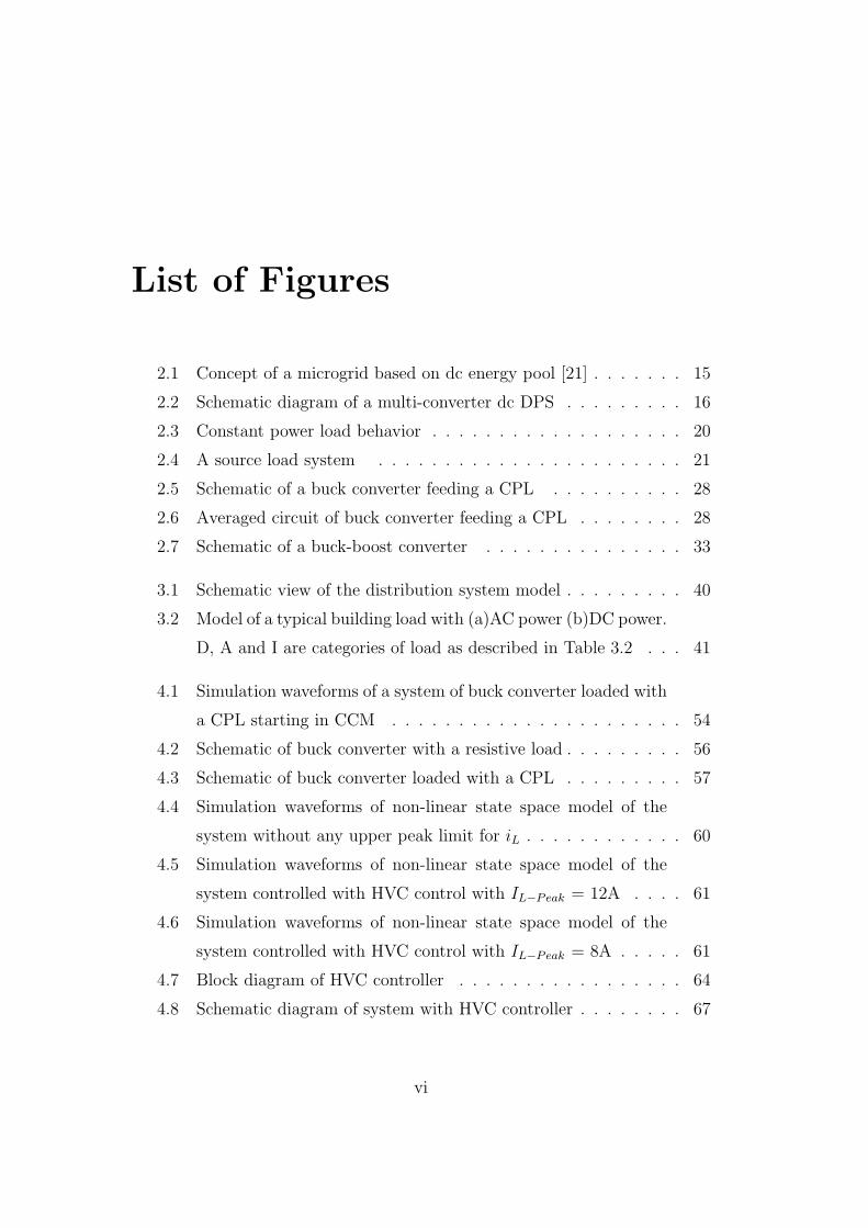
List of Figures
2.1 Concept of a microgrid based on dc energy pool [21] . . . . . . . 15
2.2 Schematic diagram of a multi-converter dc DPS . . . . . . . . . 16
2.3 Constant power load behavior . . . . . . . . . . . . . . . . . . . 20
2.4 A source load system . . . . . . . . . . . . . . . . . . . . . . . 21
2.5 Schematic of a buck converter feeding a CPL . . . . . . . . . . 28
2.6 Averaged circuit of buck converter feeding a CPL . . . . . . . . 28
2.7 Schematic of a buck-boost converter . . . . . . . . . . . . . . . 33
3.1 Schematic view of the distribution system model . . . . . . . . . 40
3.2 Model of a typical building load with (a)AC power (b)DC power.
D, A and I are categories of load as described in Table 3.2 . . . 41
4.1 Simulation waveforms of a system of buck converter loaded with
a CPL starting in CCM . . . . . . . . . . . . . . . . . . . . . . 54
4.2 Schematic of buck converter with a resistive load . . . . . . . . . 56
4.3 Schematic of buck converter loaded with a CPL . . . . . . . . . 57
4.4 Simulation waveforms of non-linear state space model of the
system without any upper peak limit for 𝑖𝐿 . . . . . . . . . . . . 60
4.5 Simulation waveforms of non-linear state space model of the
system controlled with HVC control with 𝐼𝐿−𝑃𝑒𝑎𝑘 = 12A . . . . 61
4.6 Simulation waveforms of non-linear state space model of the
system controlled with HVC control with 𝐼𝐿−𝑃𝑒𝑎𝑘 = 8A . . . . . 61
4.7 Block diagram of HVC controller . . . . . . . . . . . . . . . . . 64
4.8 Schematic diagram of system with HVC controller . . . . . . . . 67
vi
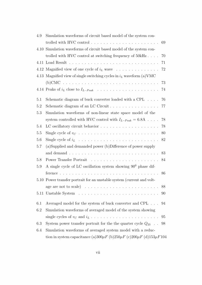
4.9 Simulation waveforms of circuit based model of the system con-
trolled with HVC control . . . . . . . . . . . . . . . . . . . . . . 69
4.10 Simulation waveforms of circuit based model of the system con-
trolled with HVC control at switching frequency of 50kHz . . . . 70
4.11 Load Result . . . . . . . . . . . . . . . . . . . . . . . . . . . . . 71
4.12 Magnified view of one cycle of 𝑖𝐿 wave . . . . . . . . . . . . . . 72
4.13 Magnified view of single switching cycles in 𝑖𝐿 waveform (a)VMC
(b)CMC . . . . . . . . . . . . . . . . . . . . . . . . . . . . . . . 73
4.14 Peaks of 𝑖𝐿 close to 𝐼𝐿−𝑃𝑒𝑎𝑘 . . . . . . . . . . . . . . . . . . . . 74
5.1 Schematic diagram of buck converter loaded with a CPL . . . . 76
5.2 Schematic diagram of an LC Circuit . . . . . . . . . . . . . . . . 77
5.3 Simulation waveforms of non-linear state space model of the
system controlled with HVC control with 𝐼𝐿−𝑃𝑒𝑎𝑘 = 6.8A . . . . 78
5.4 LC oscillatory circuit behavior . . . . . . . . . . . . . . . . . . . 78
5.5 Single cycle of 𝑣𝐶 . . . . . . . . . . . . . . . . . . . . . . . . . . 80
5.6 Single cycle of 𝑖𝐿 . . . . . . . . . . . . . . . . . . . . . . . . . . 82
5.7 (a)Supplied and demanded power (b)Difference of power supply
and demand . . . . . . . . . . . . . . . . . . . . . . . . . . . . . 83
5.8 Power Transfer Portrait . . . . . . . . . . . . . . . . . . . . . . 84
5.9 A single cycle of LC oscillation system showing 900 phase dif-
ference . . . . . . . . . . . . . . . . . . . . . . . . . . . . . . . . 86
5.10 Power transfer portrait for an unstable system (current and volt-
age are not to scale) . . . . . . . . . . . . . . . . . . . . . . . . 88
5.11 Unstable System . . . . . . . . . . . . . . . . . . . . . . . . . . 90
6.1 Averaged model for the system of buck converter and CPL . . . 94
6.2 Simulation waveforms of averaged model of the system showing
single cycles of 𝑣𝐶 and 𝑖𝐿 . . . . . . . . . . . . . . . . . . . . . . 95
6.3 System power transfer portrait for the the quarter cycle 𝑄23 . . 98
6.4 Simulation waveforms of averaged system model with a reduc-
tion in system capacitance (a)300𝜇𝐹 (b)250𝜇𝐹 (c)200𝜇𝐹 (d)153𝜇𝐹 104
vii
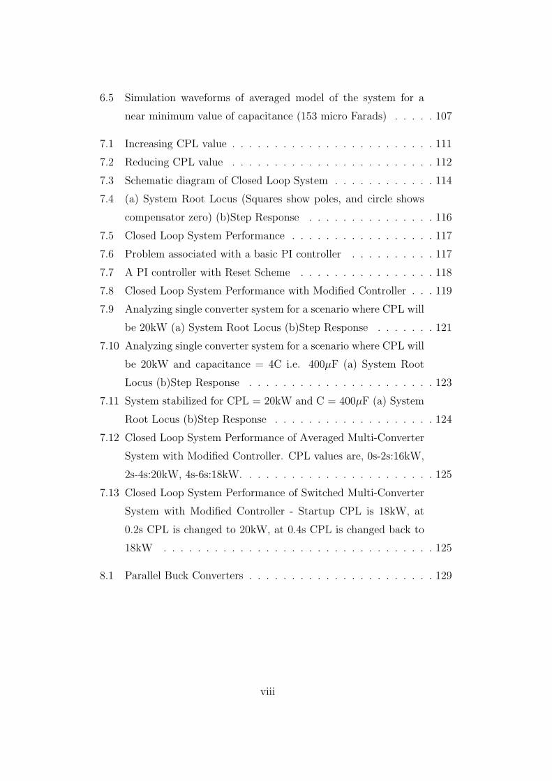
6.5 Simulation waveforms of averaged model of the system for a
near minimum value of capacitance (153 micro Farads) . . . . . 107
7.1 Increasing CPL value . . . . . . . . . . . . . . . . . . . . . . . . 111
7.2 Reducing CPL value . . . . . . . . . . . . . . . . . . . . . . . . 112
7.3 Schematic diagram of Closed Loop System . . . . . . . . . . . . 114
7.4 (a) System Root Locus (Squares show poles, and circle shows
compensator zero) (b)Step Response . . . . . . . . . . . . . . . 116
7.5 Closed Loop System Performance . . . . . . . . . . . . . . . . . 117
7.6 Problem associated with a basic PI controller . . . . . . . . . . 117
7.7 A PI controller with Reset Scheme . . . . . . . . . . . . . . . . 118
7.8 Closed Loop System Performance with Modified Controller . . . 119
7.9 Analyzing single converter system for a scenario where CPL will
be 20kW (a) System Root Locus (b)Step Response . . . . . . . 121
7.10 Analyzing single converter system for a scenario where CPL will
be 20kW and capacitance = 4C i.e. 400𝜇F (a) System Root
Locus (b)Step Response . . . . . . . . . . . . . . . . . . . . . . 123
7.11 System stabilized for CPL = 20kW and C = 400𝜇F (a) System
Root Locus (b)Step Response . . . . . . . . . . . . . . . . . . . 124
7.12 Closed Loop System Performance of Averaged Multi-Converter
System with Modified Controller. CPL values are, 0s-2s:16kW,
2s-4s:20kW, 4s-6s:18kW. . . . . . . . . . . . . . . . . . . . . . . 125
7.13 Closed Loop System Performance of Switched Multi-Converter
System with Modified Controller - Startup CPL is 18kW, at
0.2s CPL is changed to 20kW, at 0.4s CPL is changed back to
18kW . . . . . . . . . . . . . . . . . . . . . . . . . . . . . . . . 125
8.1 Parallel Buck Converters . . . . . . . . . . . . . . . . . . . . . . 129
viii
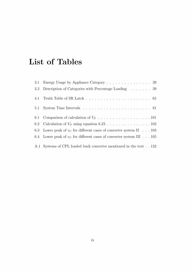
List of Tables
3.1 Energy Usage by Appliance Category . . . . . . . . . . . . . . . 39
3.2 Description of Categories with Percentage Loading . . . . . . . 39
4.1 Truth Table of SR Latch . . . . . . . . . . . . . . . . . . . . . . 65
5.1 System Time Intervals . . . . . . . . . . . . . . . . . . . . . . . 81
6.1 Comparison of calculation of 𝑉𝑃 . . . . . . . . . . . . . . . . . . 101
6.2 Calculation of 𝑉𝑃 using equation 6.23 . . . . . . . . . . . . . . . 102
6.3 Lower peak of 𝑣𝐶 for different cases of converter system II . . . 103
6.4 Lower peak of 𝑣𝐶 for different cases of converter system III . . . 105
A.1 Systems of CPL loaded buck converter mentioned in the text . . 132
ix
List of Acronyms
AC Alternating CurrentCCM Continuous Conduction Mode
CMC Current Mode Control
CPL Constant Power Load
DC Direct Current
DCM Discontinuous Conduction Mode
DG Distributed Generation
DPS Distributed Power System
EPS Electric Power System
EV Electric Vehicle
FCV Fuel Cell Vehicle
HEV Hybrid Electric Vehicle
HVC Hybrid of Voltage and Current mode control
HVDC High Voltage Direct Current
IC Internal Combustion
ISS International Space Station
LED Light Emitting Diode
LHP Left Half Plane
PD Proportional Derivative
PI Proportional Integral
PID Proportional Integral Derivative
RHP Right Half Plane
x
Abstract
Power system began its journey with DC power as pioneered by Edison. How-
ever, this was soon rivalled by AC power and ultimately DC paradigm found
itself quite obsolete, against the ongoing urge to adapt in favor of higher ef-
ficiency. AC became the choice for power transfer in all areas of the power
system namely generation, transmission, sub-transmission and distribution.
However, just as history repeats itself, the fight between these two paradigms
of power transfer was reignited as DC proved to be comparable and in certain
cases better suited for power transmission eventually leading to the acceptance
of HVDC transmission. Ironically, it was again the urge for higher efficiency
that led to the shift in the choice and this time it was the AC system which
found itself being questioned. DC power has begun a come back! Today, DC
power is increasing its amount in the generation side due to the promotion of
renewable/alternative energy sources. In this respect, solar energy may also
be noted as producing DC output as well. Wind farms is one technology which
uses AC/DC/AC conversion for connecting with the grid. Not only generation,
DC is again showing its presence in consumer load side with modern appliances
such as personal computers, laptops, mobiles, LED lighting etc. So, it can be
observed that the battle of the currents, as it is referred to, has begun again!
However, distribution system is one part of the power system where DC does
not seem to have gained ground. In recent times, this area has witnessed a
number of research efforts and DC distribution has been compared with the
AC counterpart.
In this thesis, firstly a comparison of the two paradigms is presented for
xi
xii
a residential area powered by renewable energy source. In a DC power dis-
tribution system, power electronic converters will be replacing the electrical
transformers of the AC counterpart. In this regard, a mathematical computa-
tion is presented in order to calculate the minimum required efficiency of these
power electronic converters which will make a DC system equal in efficiency
to an AC system. Despite the fact that DC distribution for residential areas
has not been widely in use, there is another area where DC is used for power
distribution and this is the DC Distributed Power System (DPS) which finds
its application in areas such as shipboard, aircraft or space station power sys-
tems. A residential DC power system, and the advance concepts of distributed
generation and DC microgrid may take advantage from research in this field.
A major issue for system designers in this field is ensuring stability of the
overall system. Constant power loads (CPLs), in such a system behave as a
negative impedance in the small signal model causing system instability. It
has been shown that a buck DC/DC converter is unstable, either operated in
voltage mode or current mode control in open loop, when loaded with a CPL.
This research presents the use of current limiting in voltage mode controlled
buck converter that can allow the system to operate without going towards
instability, effectively making the system controlled by a hybrid of voltage and
current mode control. This work goes deeper into system operation using the
hybrid technique, creating power transfer portraits of the system both when
it is stable and unstable allowing a mutual comparison. Furthermore, mathe-
matical relationships have been derived using the idea of energy balance. This
system is then operated in a closed loop and the controller design is discussed.
Finally, a multi-converter system is created and stable operation is discussed
again with regards to the controller design. Further requirements in order to
be able to simulate a DC power system or a DC microgrid have also been
presented.

Acknowledgement
All thanks go to ALLAH, The God of the worlds. It is actually His help that
I have received from various people and sources throughout the duration of
my effort towards this doctorate degree. And as is the tradition of the world,
I thank these people or sources for their time which they have given to me,
or energy which they spent for me or making me go forward one way or the
other. And this is a big list of characters. Just to mention a few of them,
the list includes my supervisor Prof. Akhtar Kalam, my sponsor university
University of Engineering and Technology Lahore, my colleagues Mr. Zaheer,
Mr. Rizwan, Mr. Waqas and Shabbir.
I would also like to acknowledge the help I received from my friend and
colleague Adul K. Mustafa in relation to compiling and formatting of this
thesis.
xiii
Chapter 1
Introduction
(Some of the content in this chapter has been presented at Australasian Uni-
versities Power Engineering Conference (AUPEC) 2009 [1]). Years ago, alter-
nating electric power outshined the direct version as the choice for a power
system [2]. Apparently, the main reason was the ability of AC to be raised or
lowered in voltage levels. This is because the equipment for allowing a change
in voltage levels was an electromagnetic transformer, and it depended on the
varying electric field which would in turn cause a varying magnetic field. This
varying magnetic field leads to power transfer between the primary and sec-
ondary windings of the transformer, and a voltage change can be achieved
based upon number of turns of the primary and secondary windings.
This electrical machine was developed for the AC voltage and currents and
allowed to raise the voltage level for longer distance transfer of power. But, it
could not be adapted for DC, since DC lacked the natural variation in voltage
levels that AC had and which was required for the transformer operation. The
DC power was too ‘direct’ to be ‘altered’.
1
2
Apparently, DC did not have any such mechanism of voltage step-up and
step-down at that time and hence, it got outbid by the AC paradigm. DC
power proposal provided by General Electric Company for the 1893 Chicago
World’s Fair, got outbid by the AC power proposal given by Westinghouse,
and around the same time DC also got outbid by AC for power generation
from Niagara Falls [2]. The era of AC began, with DC being left only for some
specialized purposes.
However, it seems that DC is finally on its return, after having solved the
problem that once got it out of business. Today, power electronic converters
can both step-up and step-down a DC voltage. DC has found its transformers.
Now after many years the age of DC seems to be on the return. In the
field of electrical power transmission, DC has already proved to be more suc-
cessful than AC. A number of transmission systems are DC now, and popular
commercially available solutions like HVDC Light by ABB, and HVDC plus
by Siemens are available.
Power generation, for which AC was assumed to be better than DC, is now
witnessing newer technologies which are inclined towards DC. These are most
notably the renewable energy technologies. Environmental concerns and fast
depleting fossil fuel reserves are increasingly forcing the world to use these
inexhaustible energy sources. Wind is perhaps the most common of all (ex-
cluding hydro energy), and a large number of wind turbine generating systems
have an intermediate DC conversion step, before they connect with the AC

3
grid. For offshore wind farms, HVDC link to onshore grid has proven to be
more successful [3].
Other than wind, photo-voltaic cells produce DC output naturally. As
more and more of these non-conventional sources get added to the system, this
increases the amount of that power in the system which has been converted to
AC from a previous DC state.
On the load side of the power system, electronic loads have witnessed a
remarkable boom in recent times. The result is a tremendous increase in DC
power consuming devices in homes and offices. These include devices like
personal computers, printers, battery chargers etc. Even the modern electric
lights are now employing internal electronic ballasts which require DC electric
power. This leaves one last field in the power system where DC is yet to make
its mark - the electrical power distribution system.
Although there already are some DC distribution systems present e.g. in
the industries, yet the overall distribution scenario especially for the residential
areas depicts alternating power only. It is this area where this thesis attempts
to present its contribution.
1.1 Importance of Power Electronic Convert-
ers in a DC Distribution System
As power electronic converters are the transformers in a DC distribution sys-
tem, they have a widespread presence. The efficiency of these converters or
4
in other words the losses occurring in these converters may be an important
deciding factor in favor or against the DC distribution paradigm as opposed
to the AC distribution.
Besides the efficiency issue of power electronic converters, another issue is
ensuring stability of the overall system. In a way, the stability issue looks easy
to deal with because in AC system the stability includes
∙ Voltage Stability
∙ Frequency Stability
∙ Rotor Angle Stability
while the DC system only has to deal with one issue i.e. voltage stability.
However, in such a multi-converter system, ensuring overall system stability is
not a simple task. In this regard, a number of research efforts, as presented
in the Literature Review, have been conducted in the stability issue of a DC
‘Distributed Power System’ - which is a specialized power system with appli-
cations such as shipboard power system, international space station, modern
electric vehicles. This thesis presents work towards the stability issue of a DC
DPS as well.
1.2 Publications
Following are publications related to this work:
5
1. F. Dastgeer and A. Kalam, “Efficiency comparison of DC and AC dis-
tribution systems for distributed generation”, Australasian Universities
Power Engineering Conference, 2009, pp. 1-5.
2. F. Dastgeer and A. Kalam, “Evolution of dc distributed power system
stability”, International Review of Electrical Engineering, part B, vol. 5,
pp. 652-662, April, 2010.
3. F. Dastgeer and A. Kalam, “Operation of an open loop buck converter
in continuous conduction mode loaded with a constant power load”, sub-
mitted for a journal publication.
1.3 Original Work
A summary of the original work presented in this thesis is as follows:
1. An efficiency comparison of DC and AC power distribution systems has
been performed and it is observed that for the assumed conditions, DC
power system has better overall efficiency.
2. A mathematical technique is presented which allows to calculate the
minimum required efficiency of power electronic converters in the DC
distribution system, so that this system can have overall efficiency at
least equal to that of a given AC distribution system.
3. A current limiting based control technique has been presented which can
allow a DC/DC buck converter loaded with a constant power load (CPL)
6
to operate without being unstable, while in open loop and in continuous
conduction mode. For the system of buck converter loaded with a CPL,
mechanism of system instability has been explored and in light of this,
how the proposed control technique (named as HVC control) keeps the
system from instability has been brought out.
4. Mathematical relationships for the upper voltage peak as well as mini-
mum required system capacitance are presented for the averaged model
of the system of buck converter loaded with CPL operating under HVC
control.
5. A multi-converter DC distributed power system has been simulated using
HVC control.
1.4 Organization of this Thesis
This thesis comprises eight chapters. Organization of the remaining seven
chapters is presented as follows:
Chapter 2 presents number of past efforts related to the current work. It
presents literature review of past attempts in the area of DC power distribu-
tion, as well as research efforts related to the stability issue of DC ‘Distributed
Power Systems’.
Chapter 3 gives an efficiency comparison of DC distribution paradigm with
its AC counterpart. Under certain conditions, it is seen that DC can be a
7
comparable distribution option to the AC power. However, a very important
parameter for the improved efficiency and hence feasibility of DC distribution
is the efficiency of its power electronic converters - the DC transformers. Sub-
sequent to the comparison, Chapter 3 presents a mathematical technique to
determine the minimum required efficiency of power electronic converters in a
DC system which makes it at least as efficient as a counterpart AC system.
From Chapter 4 onwards till Chapter 7, this thesis works on the stability
issue of a DC ‘Distributed Power System (DPS)’ concept as that may be a
potential future DC power distribution system for residential areas. Ensuring
system stability is an important issue for the DC DPS, and a lot of research
work has been performed related to this issue, some of which is discussed in
the literature review. Chapter 4 presents a control technique that can allow
a simple system of buck DC/DC converter loaded by a constant power load
to operate without being unstable while remaining in open loop in continuous
conduction mode. This is named as HVC (Hybrid of Voltage and Current
mode control) control.
In Chapter 5, further insight into HVC control is presented. This chapter
gives power transfer portraits of the system, which is a figure showing a single
cycle of voltage, current and power transferred. With the help of this portrait,
it is revealed how the system operates without going towards instability while
remaining in open loop and in continuous conduction mode.
Chapters 4 and 5 do not present related mathematical equations for the

8
HVC control technique; Chapter 6 is kept solely for these. Mathematical
equations for the system are derived on the basis of energy balance concept.
In chapter 7, there is an attempt to convert the small scale work presented
in chapters 4 - 6 to large scale so that it may be used for the bigger goal of a
DC power distribution system. This chapter begins with presenting close loop
control with HVC control. This work is then extended to a multi-converter
system and simulation results are presented.
Chapter 8 summarizes the work as well as presents future directions.
Chapter 2
Literature Review
(A certain content of this chapter has been presented at Australasian Univer-
sities Power Engineering Conference (AUPEC) 2009 [1] as well as published
in International Review of Electrical Engineering [4]). This chapter begins
by presenting some of the past research efforts in the field of DC distribution
system. Each of these is discussed with a short description, and it can be seen
that DC power distribution is not a totally new concept.
Subsequent to this, the ideas of distributed generation and microgrid are
presented. Combining these paradigms with the DC distribution concept, the
resultant concept of DC microgrid is presented towards the end of Section
2.2. A DC microgrid and the associated distribution system is composed of
power electronic converters which are a general replacement of electromagnetic
transformers of the AC distribution system. This power system, composed
of a large number of power electronic converters may be likened to a DC
‘Distributed Power System’ (DPS). These systems face the problem of ensuring
overall system stability, and the chapter presents related literature review.
9

10
Also, section 2.5 presents the concept of Constant Power Loads which is used
in the research work related to DC DPS stability.
2.1 DC Power Distribution System
A number of research efforts ([5] - [10]) related to DC distribution are presented
as follows: The author of reference [5] compares AC versus DC power for
distribution within a building. The main idea is that DC may allow a lesser
number of power conversion steps in the system. The author concludes that
DC is not feasible because of losses occurring in AC-DC conversion for each
house. However, DC is shown to be superior if local DC generation is present.
In reference [6], another in-house DC distribution scheme is discussed. Up
to three voltage levels are presented, being used at the same time. Although,
requiring a lot of wiring, this scheme reduces number of power electronic con-
verters in the house. However, the conclusion, as drawn out in this paper is
that AC is better than DC and the author points out that this scenario may
change if the grid becomes DC.
Reference [7] is a comparison of AC and DC distribution systems starting
from the grid. In this paper, different comparisons of AC and DC system
are presented by varying efficiencies of power electronic converters and voltage
levels of the system. The authors show that at very high efficiencies of DC/DC
converters and at higher voltage of DC distribution as compared to AC, DC
does become more favorable.

11
In reference [8], there is another comparison of AC and DC for low and
medium voltage distribution systems. At the end of the paper, the conclusion
is that the DC system can perform better if the losses in semiconductor devices
are reduced by half.
The authors of reference [9] discuss feasibility of a DC system for com-
mercial facilities. They assume that components for DC system are available
in the market, and conclude 325 Volts as the most suitable voltage level for
distribution within the facility, both technically and economically.
In reference [10], the authors determine maximum power transfer capability
through continuation power flow method, of two DC systems, one with two
lines and the other with three lines and an AC system. According to them the
three wire DC system is ideal for replacing the AC system, as AC system has
three lines as well. They conclude that by the use of DC, as much as tenfold
increase can be achieved in the transmittable power.
The research effort discussed so far indicate that the concept of DC power
distribution has been investigated in the past. The next section combines this
idea with the modern concepts of microgrids.
2.2 Distributed Generation and Microgrids
The conventional power system may be compared to an irrigation system which
has rivers as main reservoirs of water. From these rivers, canals draw large
amount of water and bring it to different villages. Each village then draws its

12
own smaller tributary from the main canal and this tributary runs within the
village. From this tributary, different fields are irrigated.
A conventional power system has centralized power generation such as dams
or large thermal power plants. These are connected to the transmission system
(like canals of the irrigation system), which brings power to the outskirts of
a city. To this system, the local distribution system of the city is connected
which provides power to its buildings (similar to the within village tributary).
However, with the passage of time, the villagers realize that the tributary
is not the only source of water they are bound to. A second source may be
the very earth they irrigate. They begin to use electrical tubewells and draw
water from the depths of the earth.
In a similar way, the modern human being realizes the importance of re-
newable energy sources such as sun light or wind, as compared to fossil fuels.
Power generators based on these technologies are now being connected to the
power system on the distribution side. This paradigm of connecting power
generators on the distribution side of the power system is referred to as Dis-
tributed Generation (DG), and is not limited to renewable power sources as
conventional power generators such as gas turbines or IC engines may be used
as well [11] to achieve the benefits of this paradigm. Despite certain problem-
atic issues ([13] - [15]) , DG offers benefits as listed in reference [11]:
∙ Reduced line losses

13
∙ Enhanced system reliability and security
∙ Relieved T & D congestion
∙ Increased security for critical loads
∙ Reduced emission of pollutants
∙ Reduced reserve requirements and associated costs
Besides the advantages of distributed generation, reference [12] mentions
that further development is required in order to properly connect these new
systems into the existing power system which was not designed to support
active power generation at distribution level.
An idea of a microgrid was developed which will feed a certain locality
based upon a power generating system available on the spot [16]. A microgrid
is an entity in a power system having its own power generation and utilization,
that can operate with or without the connection to the main power system. It
can be composed of several types of devices as mentioned in reference [16]:
∙ power plants
∙ loads (controlled or uncontrolled by microgrid controller)
∙ energy storage units
∙ control system
∙ telecommunication lines
14
The idea of microgrid has seen a lot of research efforts in recent times,
some of the references are [16]-[21]. However, besides the usual AC microgrid;
a number of research efforts on DC microgrids exist as well ([16], [20], [21]).
Reference [20] investigates the idea of a DC microgrid for residential houses
with each house having a cogeneration system. The authors mention that
their results show that the system could supply high quality power to the
loads against sudden load variation.
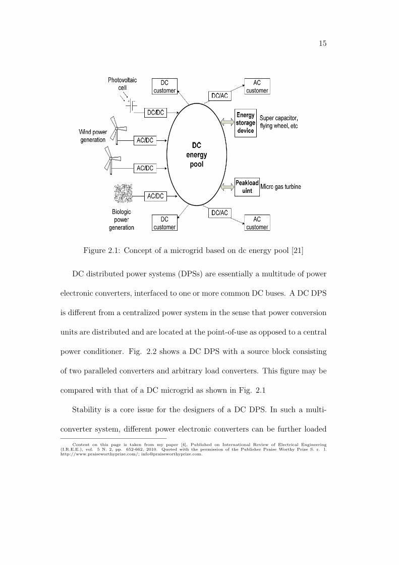
Reference [21] present the concept of a microgrid based on a DC energy
pool. Fig. 2.1 presents the idea of the authors. The authors mention that
energy from all the sources is be converted into DC and fed into the DC
energy supplying network. The DC consumers take power directly while the
AC customers take power after an inversion stage. Energy storage elements
are there to cater for any mismatch between supply and demand of power.
2.3 DC Distributed Power System and its
Stability Issue
DC microgrids may be compared to another form of power distribution system
known as ‘Distributed Power System’ (DPS). Despite the fact that these sys-
tems have existed for quite a while by now, they are relatively unknown to a
conventional power engineer because they have other specialized applications
as presented in the next section.
15
Figure 2.1: Concept of a microgrid based on dc energy pool [21]
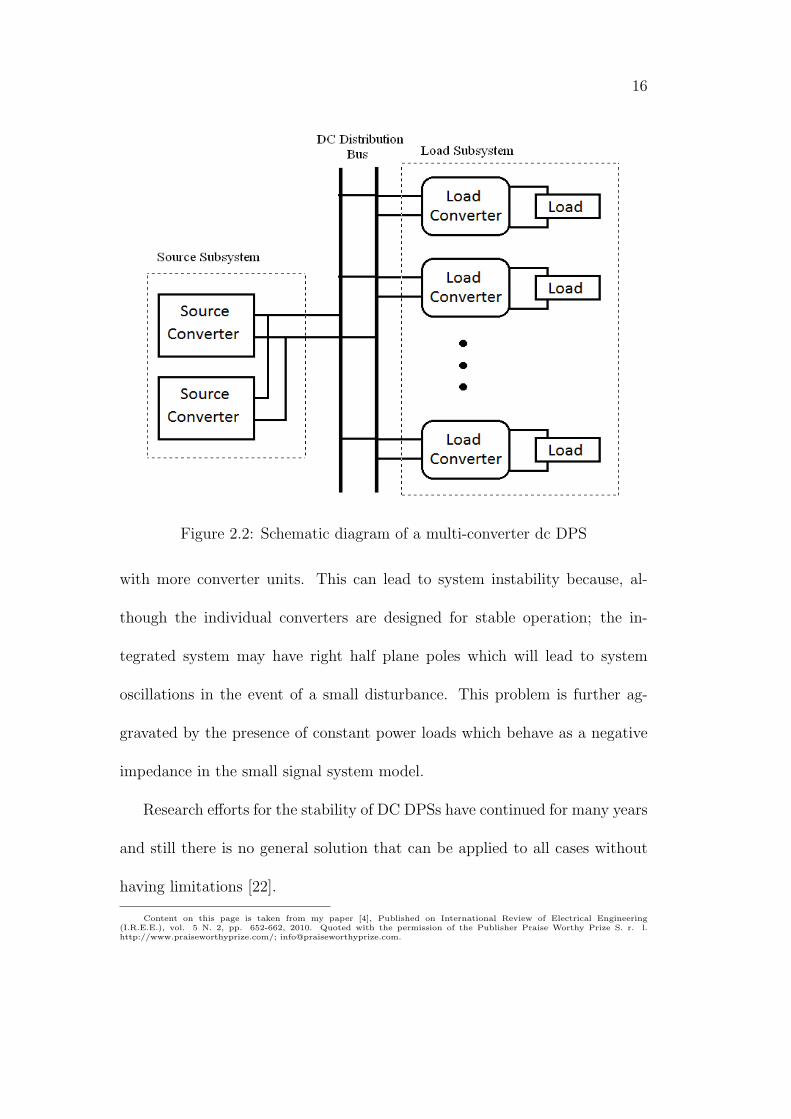
DC distributed power systems (DPSs) are essentially a multitude of power
electronic converters, interfaced to one or more common DC buses. A DC DPS
is different from a centralized power system in the sense that power conversion
units are distributed and are located at the point-of-use as opposed to a central
power conditioner. Fig. 2.2 shows a DC DPS with a source block consisting
of two paralleled converters and arbitrary load converters. This figure may be
compared with that of a DC microgrid as shown in Fig. 2.1
Stability is a core issue for the designers of a DC DPS. In such a multi-
converter system, different power electronic converters can be further loaded
Content on this page is taken from my paper [4], Published on International Review of Electrical Engineering(I.R.E.E.), vol. 5 N. 2, pp. 652-662, 2010. Quoted with the permission of the Publisher Praise Worthy Prize S. r. l.http://www.praiseworthyprize.com/; [email protected].
16
Figure 2.2: Schematic diagram of a multi-converter dc DPS
with more converter units. This can lead to system instability because, al-
though the individual converters are designed for stable operation; the in-
tegrated system may have right half plane poles which will lead to system
oscillations in the event of a small disturbance. This problem is further ag-
gravated by the presence of constant power loads which behave as a negative
impedance in the small signal system model.
Research efforts for the stability of DC DPSs have continued for many years
and still there is no general solution that can be applied to all cases without
having limitations [22].
Content on this page is taken from my paper [4], Published on International Review of Electrical Engineering(I.R.E.E.), vol. 5 N. 2, pp. 652-662, 2010. Quoted with the permission of the Publisher Praise Worthy Prize S. r. l.http://www.praiseworthyprize.com/; [email protected].
17
Literature review related to the stability issue of DC DPS is presented
subsequent to the next two sections, the first of which presents applications of
DPS and the second discusses the concept of Constant Power Loads.
2.4 Applications of DC Distributed Power
Systems
DC DPS finds applications such as mainframe computers and similar electronic
devices. Following are some of the major high power applications of a DC DPS:
2.4.1 The International Space Station
The international space station electric power system (ISS EPS) may be re-
garded as one of the earliest highly multi-connected applications of a DC DPS.
It was a complex system consisting of a fairly large number of DC/DC con-
verters, back-up batteries and their associated charge/discharge units. The
complete architecture consisted of both the 120-V American and 28-V Russian
electrical networks, which were capable of exchanging power through dedicated
isolating converters [23]. The system consisted of a higher voltage primary and
a lower voltage more tightly regulated secondary DC bus.
2.4.2 Shipboard Power Systems
Naval shipboard power systems are another area where DC distributed power
system has found its application. Navies focus on zonal approach for the power
Content on this page is taken from my paper [4], Published on International Review of Electrical Engineering(I.R.E.E.), vol. 5 N. 2, pp. 652-662, 2010. Quoted with the permission of the Publisher Praise Worthy Prize S. r. l.http://www.praiseworthyprize.com/; [email protected].
18
system where various zones separated by watertight bulkheads are powered by
dedicated DC/DC converters [24]. In such a distribution system, AC power
is first rectified to high voltage DC which is routed to different zones via the
high voltage DC bus. Buck converters of individual zones, then convert this
power according to the needs of loads of the zone [24].
2.4.3 Advanced Automobiles
Advanced automobile power systems are a relatively new and highly researched
application of DC DPS. The trend of using electric power for the automobile
propulsion system has brought forth new concepts such as electric vehicles
(EVs), hybrid electric vehicles (HEVs) and fuel cell vehicles (FCVs). EVs use
batteries and super capacitors for energy storage, however, there is no gen-
eration of energy. On the contrary FCVs use fuel cells for energy generation
which can be supplied to the system loads and/or it may be stored in bat-
tery units connected to the main DC bus via charge/discharge converters or
ultra-capacitors. In HEVs, conventional heat engine is present and its torque
is mechanically coupled with the torque of electric propulsion system. High
voltage DC is required by the electric traction system necessitating an HVDC
bus. Overall, the power system is a multitude of power electronic converters
interfaced to one or more DC buses.
Content on this page is taken from my paper [4], Published on International Review of Electrical Engineering(I.R.E.E.), vol. 5 N. 2, pp. 652-662, 2010. Quoted with the permission of the Publisher Praise Worthy Prize S. r. l.http://www.praiseworthyprize.com/; [email protected].
19
2.5 Constant Power Loads
Power electronic converters with the requirement to maintain a constant value
of output voltage and current increase/decrease their input current as in-
put voltage decreases/increases respectively. This behavior is termed as con-
stant power load (CPL) behavior and is opposite to that of a normal resistive
load which increases/decreases its current as input voltage increases/decreases.
Converter bandwidth plays an important role in this behavior with higher
bandwidths leading towards ideal CPL behavior. A simple example of a CPL
can be a DC motor drive which needs to provide a constant torque and a fixed
rotational speed to the mechanical load. The drive will therefore sink constant
power from its source which will lead to an increased current input if the input
voltage drops and vice versa.
In small signal model, constant power loads show a negative impedance
behavior. This unconventional behavior arises from the fact that, although the
instantaneous impedance is always positive at any given time, the incremental
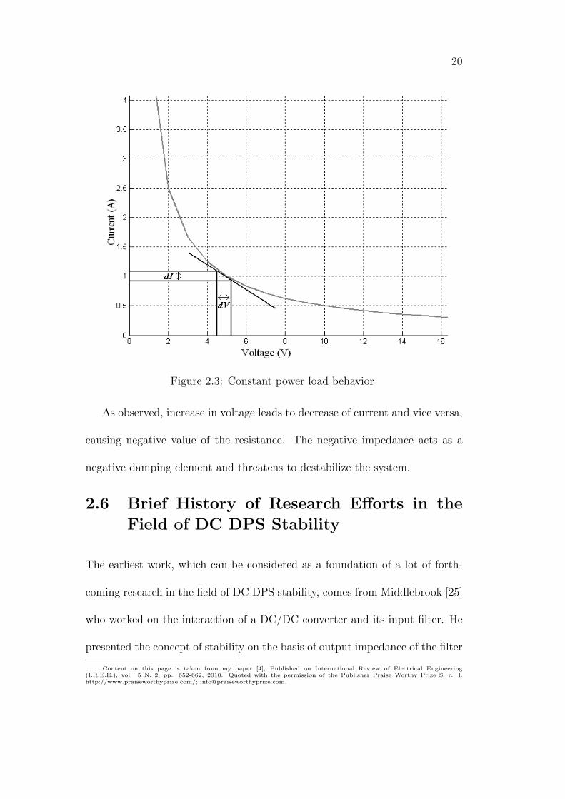
value is negative. Fig. 2.3 shows the constant power behavior of a load (5
Watts) on VI axes plane. The CPL curve is linearized at a point and the
incremental resistance is given as
𝑑𝑉
𝑑𝐼< 0 (2.1)
Content on this page is taken from my paper [4], Published on International Review of Electrical Engineering(I.R.E.E.), vol. 5 N. 2, pp. 652-662, 2010. Quoted with the permission of the Publisher Praise Worthy Prize S. r. l.http://www.praiseworthyprize.com/; [email protected].
20
Figure 2.3: Constant power load behavior
As observed, increase in voltage leads to decrease of current and vice versa,
causing negative value of the resistance. The negative impedance acts as a
negative damping element and threatens to destabilize the system.
2.6 Brief History of Research Efforts in the
Field of DC DPS Stability
The earliest work, which can be considered as a foundation of a lot of forth-
coming research in the field of DC DPS stability, comes from Middlebrook [25]
who worked on the interaction of a DC/DC converter and its input filter. He
presented the concept of stability on the basis of output impedance of the filter
Content on this page is taken from my paper [4], Published on International Review of Electrical Engineering(I.R.E.E.), vol. 5 N. 2, pp. 652-662, 2010. Quoted with the permission of the Publisher Praise Worthy Prize S. r. l.http://www.praiseworthyprize.com/; [email protected].
21
and input impedance of the DC/DC converter, in other words the impedances
at the interface. This concept was later extended and applied to the stability
of a DC/DC converter source block feeding a certain load.
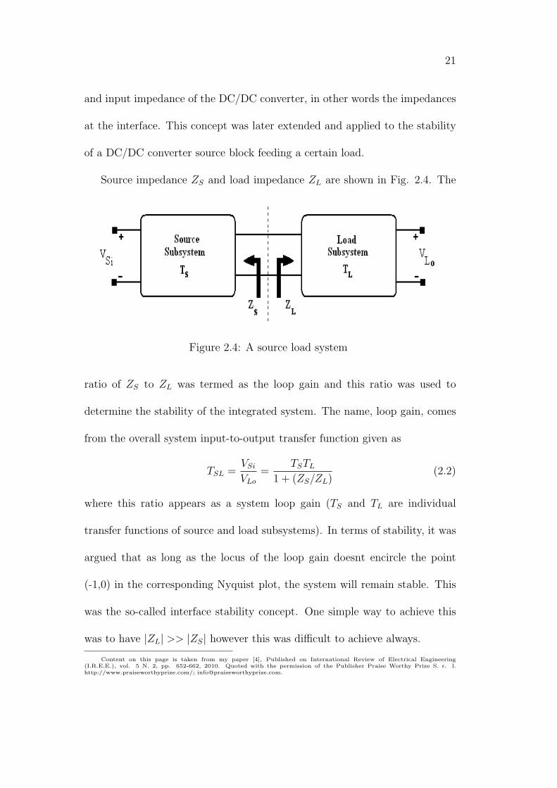
Source impedance 𝑍𝑆 and load impedance 𝑍𝐿 are shown in Fig. 2.4. The
Figure 2.4: A source load system
ratio of 𝑍𝑆 to 𝑍𝐿 was termed as the loop gain and this ratio was used to
determine the stability of the integrated system. The name, loop gain, comes
from the overall system input-to-output transfer function given as
𝑇𝑆𝐿 =𝑉𝑆𝑖
𝑉𝐿𝑜
=𝑇𝑆𝑇𝐿
1 + (𝑍𝑆/𝑍𝐿)(2.2)
where this ratio appears as a system loop gain (𝑇𝑆 and 𝑇𝐿 are individual
transfer functions of source and load subsystems). In terms of stability, it was
argued that as long as the locus of the loop gain doesnt encircle the point
(-1,0) in the corresponding Nyquist plot, the system will remain stable. This
was the so-called interface stability concept. One simple way to achieve this
was to have ∣𝑍𝐿∣ >> ∣𝑍𝑆∣ however this was difficult to achieve always.
Content on this page is taken from my paper [4], Published on International Review of Electrical Engineering(I.R.E.E.), vol. 5 N. 2, pp. 652-662, 2010. Quoted with the permission of the Publisher Praise Worthy Prize S. r. l.http://www.praiseworthyprize.com/; [email protected].
22
The interface stability concept gained profound attention with the devel-
opment of the International Space Station in the mid 90’s [23, 26]. The ISS
electric power system (EPS) was one of the most complex DC distributed
power systems of its time.
The ISS EPS engineers decided in favor of using the interface impedance
ratio method for assessing the stability of the system as mentioned in reference
[26]. A couple of years later, a major development for this method was made
by the authors of reference [27] who provided a practical way which could be
used to integrate large systems based upon modular approach. These authors
assumed that 𝑍𝑆 is known for a system and they developed a criterion for the
input impedance of a load to be connected to this source such that the overall
source load system remains stable. This criterion was based upon the idea of
unacceptable phase bands on Bode plots for the input impedance of the load.
If the phase of 𝑍𝐿 did not enter these unacceptable bands in the phase plot,
the system would be stable, even if ∣𝑍𝑆∣ > ∣𝑍𝐿∣ at these frequencies. This
unacceptable phase band was given by the expression
1800 − 𝑃𝑀1 < ∠𝑍𝑆 − ∠𝑍𝐿 < 1800 + 𝑃𝑀2 (2.3)
The two phase margins (PM) were assumed to be 600 by the authors.
This approach was taken up by the designers of the ISS as mentioned in
reference [23]. However, as pointed out by the authors of reference [23], the
Content on this page is taken from my paper [4], Published on International Review of Electrical Engineering(I.R.E.E.), vol. 5 N. 2, pp. 652-662, 2010. Quoted with the permission of the Publisher Praise Worthy Prize S. r. l.http://www.praiseworthyprize.com/; [email protected].

23
impedance stability technique, is a small signal technique and it did not ensure
large signal stability. The authors mention that practical, analytical tools for
ensuring large signal stability did not exist at that time, and for this task the
ISS EPS team needed to include computer simulations and hardware testing
in the system design.
The impedance stability criterion witnessed different small scale contribu-
tions in its near future. The authors of reference [28] extended this concept to
the case of multiple DC/DC converter sources paralleled together with master-
slave current sharing. They derive expressions for individual source output
admittances and design current sharing loop compensator for a stable system.
In reference [29] the authors elaborated the forbidden region concept presented
in reference [27] for a composite load, to the individual load modules of a com-
posite load. On a Nyquist plot of 𝑍𝑆/𝑍𝐿𝐾 , where 𝑍𝐿𝐾 is the input impedance
of the kth load, this newly defined forbidden region for the kth load of the
system was
𝑅𝑒(𝑍𝑆
𝑍𝐿𝐾
) ≥= −1
2
𝑃𝑙𝑜𝑎𝑑−𝑘
𝑃𝑠𝑜𝑢𝑟𝑐𝑒
(2.4)
𝑃𝑠𝑜𝑢𝑟𝑐𝑒 and 𝑃𝑙𝑜𝑎𝑑−𝑘 are the power levels of the source and kth load respectively.
The corresponding allowable phase band on a Bode plot was given as
−900 − 𝜙𝑘 < ∠𝑍𝑆 − ∠𝑍𝐿𝑘 < 900 + 𝜙𝑘 (2.5)
Content on this page is taken from my paper [4], Published on International Review of Electrical Engineering(I.R.E.E.), vol. 5 N. 2, pp. 652-662, 2010. Quoted with the permission of the Publisher Praise Worthy Prize S. r. l.http://www.praiseworthyprize.com/; [email protected].
24
where
𝜙𝑘 = 𝑎𝑟𝑐𝑠𝑖𝑛
∣∣∣∣12𝑍𝐿𝑘𝑃𝑙𝑜𝑎𝑑−𝑘
𝑍𝑆𝑃𝑠𝑜𝑢𝑟𝑐𝑒
∣∣∣∣ (2.6)
The authors of reference [30] present a practical way to measure the sta-
bility margins of a system by online monitoring of the loop gain of a system.
They choose 𝑆(𝜔) which is distance between the point (-1,0) and loop gain
locus on the Nyquist plot as a quantifiable index of the stability margin and
evaluate this by connecting an external perturbation current source 𝑖𝑝(𝑗𝜔) to
the DC bus and measuring the response current 𝑖𝑠(𝑗𝜔) of the system. 𝑆(𝜔) is
calculated as
𝑆(𝜔) =
∣∣∣∣ 𝑖𝑝(𝑗𝜔)𝑖𝑠(𝑗𝜔)
∣∣∣∣ (2.7)
Flanking the development of interface impedance stability criterion, there
were other researches being carried out for stabilizing the system based upon
classical and advanced control techniques. It was this stream of research which
was later carried on in the 21st century while the former approach could not
gain popularity. Because of the detailed involvement of transfer functions of
individual converters, this approach was initially limited to only a few con-
verters.
In reference [31] the authors present dynamics of a buck converter feeding
a constant power load. They derive the line to output transfer function for
Content on this page is taken from my paper [4], Published on International Review of Electrical Engineering(I.R.E.E.), vol. 5 N. 2, pp. 652-662, 2010. Quoted with the permission of the Publisher Praise Worthy Prize S. r. l.http://www.praiseworthyprize.com/; [email protected].
25
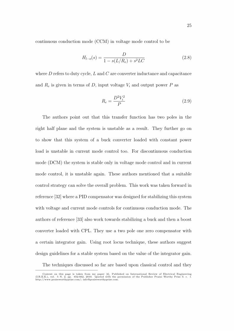
continuous conduction mode (CCM) in voltage mode control to be
𝐻𝑙−𝑜(𝑠) =𝐷
1− 𝑠(𝐿/𝑅𝑒) + 𝑠2𝐿𝐶(2.8)
where𝐷 refers to duty cycle, 𝐿 and 𝐶 are converter inductance and capacitance
and 𝑅𝑒 is given in terms of 𝐷, input voltage 𝑉𝑖 and output power 𝑃 as
𝑅𝑒 =𝐷2𝑉 2
𝑖
𝑃(2.9)
The authors point out that this transfer function has two poles in the
right half plane and the system is unstable as a result. They further go on
to show that this system of a buck converter loaded with constant power
load is unstable in current mode control too. For discontinuous conduction
mode (DCM) the system is stable only in voltage mode control and in current
mode control, it is unstable again. These authors mentioned that a suitable
control strategy can solve the overall problem. This work was taken forward in
reference [32] where a PID compensator was designed for stabilizing this system
with voltage and current mode controls for continuous conduction mode. The
authors of reference [33] also work towards stabilizing a buck and then a boost
converter loaded with CPL. They use a two pole one zero compensator with
a certain integrator gain. Using root locus technique, these authors suggest
design guidelines for a stable system based on the value of the integrator gain.
The techniques discussed so far are based upon classical control and they
Content on this page is taken from my paper [4], Published on International Review of Electrical Engineering(I.R.E.E.), vol. 5 N. 2, pp. 652-662, 2010. Quoted with the permission of the Publisher Praise Worthy Prize S. r. l.http://www.praiseworthyprize.com/; [email protected].
26
attempted to ensure small signal stability of the system. Large signal stabil-
ity still remained a challenging issue. This was dealt with the initiation of
using advanced non-linear control techniques for DC DPS stability. One of
these was sliding mode control explained for a Cuk converter in reference [34].
The second is feedback linearization as presented in reference [35, 36]. Unlike
the usual process of linearization based upon Taylors series, the idea here is
to choose such a non-linear control as can cancel out the non-linearity of the
open loop system, so that the closed loop system becomes linear. This tech-
nique attempted to establish feedback control based on non-linear coordinate
transformation and tried to ensure an extended region of local stability [36].
After presenting this technique for a single buck converter loaded with a CPL,
the authors extended it to two buck converters operating in parallel with equal
current sharing. However this technique was later compared to the advanced
synergetic control in reference [37] which showed superior performance besides
boasting handling of system multi-connectivity and high-dimensionality. The
pros and cons of synergetic control as well as other modern techniques for DC
DPS stability are discussed in the following sections:
2.7 Phase Plane Analysis
Phase plane analysis as described by authors of references [24], [38], [39] is a
large signal technique which attempts to describe how large is large; i.e. how
Content on this page is taken from my paper [4], Published on International Review of Electrical Engineering(I.R.E.E.), vol. 5 N. 2, pp. 652-662, 2010. Quoted with the permission of the Publisher Praise Worthy Prize S. r. l.http://www.praiseworthyprize.com/; [email protected].
27
large can a large signal disturbance be for the system to regain stability after
the transient. This technique determines a subset (called basin of attraction)
of operating points in the super set of all possible operating points; so that
this subset represents the stable region in the system state space. In other
words, if the system is perturbed from its equilibrium operating point, but the
shift in operating point does not move it beyond the basin of attraction, it
will return to the equilibrium operating point. However, if the operating point
is moved to a region outside the basin of attraction, this will lead to system
instability as the operating point will not return to the equilibrium value.
This is because of divergent nature of system state space trajectories outside
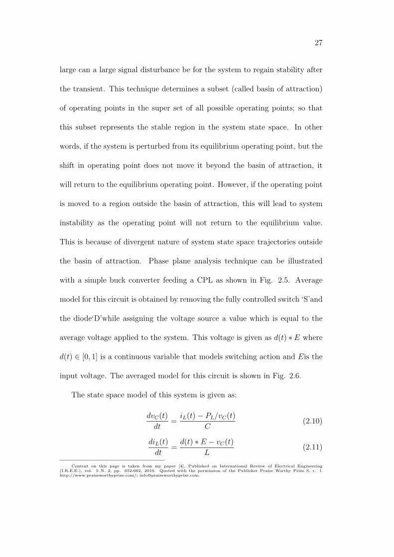
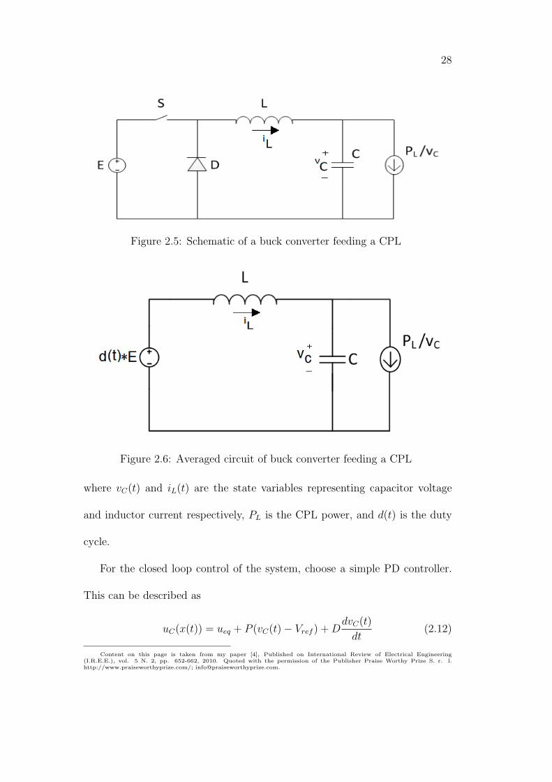
the basin of attraction. Phase plane analysis technique can be illustrated
with a simple buck converter feeding a CPL as shown in Fig. 2.5. Average
model for this circuit is obtained by removing the fully controlled switch ‘S’and
the diode‘D’while assigning the voltage source a value which is equal to the
average voltage applied to the system. This voltage is given as 𝑑(𝑡) ∗𝐸 where
𝑑(𝑡) ∈ [0, 1] is a continuous variable that models switching action and 𝐸is the
input voltage. The averaged model for this circuit is shown in Fig. 2.6.
The state space model of this system is given as:
𝑑𝑣𝐶(𝑡)
𝑑𝑡=
𝑖𝐿(𝑡)− 𝑃𝐿/𝑣𝐶(𝑡)
𝐶(2.10)
𝑑𝑖𝐿(𝑡)
𝑑𝑡=
𝑑(𝑡) ∗ 𝐸 − 𝑣𝐶(𝑡)
𝐿(2.11)
Content on this page is taken from my paper [4], Published on International Review of Electrical Engineering(I.R.E.E.), vol. 5 N. 2, pp. 652-662, 2010. Quoted with the permission of the Publisher Praise Worthy Prize S. r. l.http://www.praiseworthyprize.com/; [email protected].
28
Figure 2.5: Schematic of a buck converter feeding a CPL
Figure 2.6: Averaged circuit of buck converter feeding a CPL
where 𝑣𝐶(𝑡) and 𝑖𝐿(𝑡) are the state variables representing capacitor voltage
and inductor current respectively, 𝑃𝐿 is the CPL power, and 𝑑(𝑡) is the duty
cycle.
For the closed loop control of the system, choose a simple PD controller.
This can be described as
𝑢𝐶(𝑥(𝑡)) = 𝑢𝑒𝑞 + 𝑃 (𝑣𝐶(𝑡)− 𝑉𝑟𝑒𝑓 ) +𝐷𝑑𝑣𝐶(𝑡)
𝑑𝑡(2.12)
Content on this page is taken from my paper [4], Published on International Review of Electrical Engineering(I.R.E.E.), vol. 5 N. 2, pp. 652-662, 2010. Quoted with the permission of the Publisher Praise Worthy Prize S. r. l.http://www.praiseworthyprize.com/; [email protected].
29
where 𝑃 and 𝐷 are proportional and derivative gains, 𝑉𝑟𝑒𝑓 is the required
output voltage, 𝑥(𝑡) = (𝑣𝐶 , 𝑖𝐿)𝑇 and
𝑢𝑒𝑞 =𝑉𝑟𝑒𝑓
𝐸(2.13)
Based upon the definitions of control algorithm and d(t), there are three
possible scenarios;
𝑑(𝑡) = 𝑢𝐶(𝑥(𝑡)) 𝑖𝑓 𝑢𝐶 ∈ (0, 1) (2.14)
𝑑(𝑡) = 0 𝑖𝑓 𝑢𝑐 < 0 (2.15)
𝑑(𝑡) = 1 𝑖𝑓 𝑢𝑐 > 0 (2.16)
Corresponding to these values for 𝑑(𝑡), the system state space can be divided
into three regions of operation.
𝑋0 = {𝑥(𝑡) : 𝑑(𝑡) = 0} (2.17)
𝑋1 = {𝑥(𝑡) : 𝑑(𝑡) = 1} (2.18)
𝑋01 = {𝑥(𝑡) : 𝑑(𝑡) ∈ (0, 1)} (2.19)
The equilibrium operating point as well as the global state trajectories
can now be analyzed by the three sets of differential equations created by
substituting equations of 𝑑(𝑡) in the system model. This creates the overall
state space depiction of the system named as phase portrait of the system.
Once the phase portrait is created, the basin of attraction is the region in
which all state trajectories converge to the equilibrium operating point.
Content on this page is taken from my paper [4], Published on International Review of Electrical Engineering(I.R.E.E.), vol. 5 N. 2, pp. 652-662, 2010. Quoted with the permission of the Publisher Praise Worthy Prize S. r. l.http://www.praiseworthyprize.com/; [email protected].

30
Reviewing phase plane analysis technique, it is noticed that this is merely
an analysis technique and does not deal with control synthesis for stabiliz-
ing the system. Also, apparently this technique has only been applied to a
single source converter feeding a load. However, in practice there are many
applications where source converters need to be paralleled and in such a case,
the system contains as many state variables as the number of paralleled con-
verters plus one. Since the number of states has increased, the application
and visualization of phase plane analysis technique becomes challenging once
again.
2.8 Synergetic Control
Control design for a DC distributed power system is plagued with problems
such as non-linearity, multi-connectivity and high dimensionality [40]. Classi-
cal control techniques find it difficult to struggle with all these issues of this
complex system. Advanced techniques like sliding mode control [34] and feed-
back linearization [36] attempt to mitigate the problem of non-linearity; how-
ever the high order system dimensionality as well as the multiple connectivity
still remain challenging issues.
Synergetic control technique [37], [40]-[42] attempts to tackle all these issues
simultaneously. This technique is based upon the relatively new synergetic
control theory. It utilizes dissipative structure algorithms and provides an
Content on this page is taken from my paper [4], Published on International Review of Electrical Engineering(I.R.E.E.), vol. 5 N. 2, pp. 652-662, 2010. Quoted with the permission of the Publisher Praise Worthy Prize S. r. l.http://www.praiseworthyprize.com/; [email protected].
31
analytical approach to control design for systems which are non-linear, multi-
connected and highly dimensional [37]. However, here synergetic control theory
is only described as applied to the DC DPS.
Synergetic control uses a non-linear system model and attempts to ensure
a global or semi-global asymptotic stability [40]. It is based upon state space
system modeling and it transforms the original or modified state space model
into a new set of variables called macro-variables. These are then converted to
manifolds and the control task is to move the system in an asymptotically sta-
ble way towards the manifolds and then along the manifolds to the equilibrium
point. To ensure stability, this technique derives stability conditions.
Considering the comparison of synergetic control technique with other tech-
niques, large signal approach is what puts synergetic control ahead of classical
control which designed the system for small signal stability. As mentioned by
the authors of reference [23] working for the International Space Station, large
signal stability could not be guaranteed by their techniques and they had to
resort to hardware testing and extensive computer simulation to complete the
stability triad. This also shows superiority of synergetic control to the mod-
ern techniques of Pulse Adjustment Control and system damping variation as
explained subsequently, as these techniques also ensure stability based upon
Content on this page is taken from my paper [4], Published on International Review of Electrical Engineering(I.R.E.E.), vol. 5 N. 2, pp. 652-662, 2010. Quoted with the permission of the Publisher Praise Worthy Prize S. r. l.http://www.praiseworthyprize.com/; [email protected].
32
small signal modeling of the system. However, despite its advantages of supe-
rior performance and designing control for complex systems, synergetic control
technique shows oscillatory behavior for output voltage in discontinuous con-
duction mode [37] and this needs to be mitigated by different techniques.
2.9 Pulse Adjustment Control Technique
Pulse adjustment control [45]-[47] is one of the latest control schemes designed
for control and stabilization of converters loaded with CPLs. This digital con-
trol technique stands out from the rest in the sense that it utilizes two different
values of duty cycle for the same converter. It operates the converter in dis-
continuous conduction mode which is its second most distinguishing feature.
Pulse adjustment control technique, demonstrated for buck-boost convert-
ers, forces the converter to produce a number of high power and low power
pulses in a certain time period. The low power pulse (LP), based upon the
smaller duty cycle is designed so as to extract lesser energy from the converter
voltage source than is required by the load. This causes output voltage to be
reduced. The high power pulse (HP), based upon larger duty cycle works in
the opposite manner and increases the output voltage. As a result, the pulse
train of both these duty cycles maintains the output voltage within a small
fluctuation of reference voltage.
For the buck-boost converter shown in Fig. 2.7, the equation for variation
Content on this page is taken from my paper [4], Published on International Review of Electrical Engineering(I.R.E.E.), vol. 5 N. 2, pp. 652-662, 2010. Quoted with the permission of the Publisher Praise Worthy Prize S. r. l.http://www.praiseworthyprize.com/; [email protected].
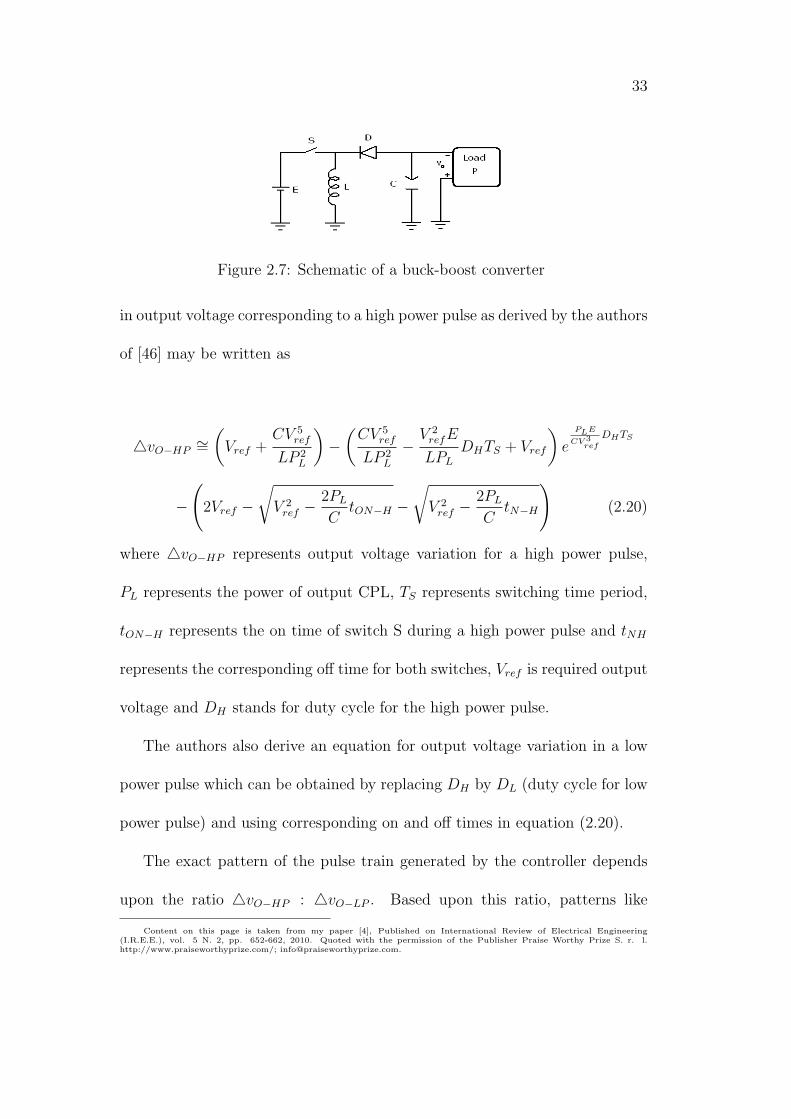
33
Figure 2.7: Schematic of a buck-boost converter
in output voltage corresponding to a high power pulse as derived by the authors
of [46] may be written as
△𝑣𝑂−𝐻𝑃∼=(𝑉𝑟𝑒𝑓 +
𝐶𝑉 5𝑟𝑒𝑓
𝐿𝑃 2𝐿
)−(𝐶𝑉 5
𝑟𝑒𝑓
𝐿𝑃 2𝐿
− 𝑉 2𝑟𝑒𝑓𝐸
𝐿𝑃𝐿
𝐷𝐻𝑇𝑆 + 𝑉𝑟𝑒𝑓
)𝑒
𝑃𝐿𝐸
𝐶𝑉 3𝑟𝑒𝑓
𝐷𝐻𝑇𝑆
−(2𝑉𝑟𝑒𝑓 −
√𝑉 2𝑟𝑒𝑓 −
2𝑃𝐿
𝐶𝑡𝑂𝑁−𝐻 −
√𝑉 2𝑟𝑒𝑓 −
2𝑃𝐿
𝐶𝑡𝑁−𝐻
)(2.20)
where △𝑣𝑂−𝐻𝑃 represents output voltage variation for a high power pulse,
𝑃𝐿 represents the power of output CPL, 𝑇𝑆 represents switching time period,
𝑡𝑂𝑁−𝐻 represents the on time of switch S during a high power pulse and 𝑡𝑁𝐻
represents the corresponding off time for both switches, 𝑉𝑟𝑒𝑓 is required output
voltage and 𝐷𝐻 stands for duty cycle for the high power pulse.
The authors also derive an equation for output voltage variation in a low
power pulse which can be obtained by replacing 𝐷𝐻 by 𝐷𝐿 (duty cycle for low
power pulse) and using corresponding on and off times in equation (2.20).
The exact pattern of the pulse train generated by the controller depends
upon the ratio △𝑣𝑂−𝐻𝑃 : △𝑣𝑂−𝐿𝑃 . Based upon this ratio, patterns like
Content on this page is taken from my paper [4], Published on International Review of Electrical Engineering(I.R.E.E.), vol. 5 N. 2, pp. 652-662, 2010. Quoted with the permission of the Publisher Praise Worthy Prize S. r. l.http://www.praiseworthyprize.com/; [email protected].
34
1HP:1LP, 1HP:3LP and 2HP:1LP can be generated for ratio values of 1, 3 and
0.5 respectively. To analyze system stability using pulse adjustment control
technique, the authors of reference [46] develop a small signal averaged model
of the buck-boost converter loaded with a CPL and controlled by the two duty
cycles 𝐷𝐻 and 𝐷𝐿. They derive the final condition for system stability to be
𝑇𝑆𝑉2𝑖𝑛
2𝐿𝐷2
𝐿 < 𝑃𝐿 <𝑇𝑆𝑉
2𝑖𝑛
2𝐿𝐷2
𝐻 (2.21)
This is the range of CPL loads for which the controller can maintain output
voltage and stabilize the system. The authors demonstrate this technique via
simulation results.
Reviewing the pulse adjustment control technique, it is observed that the
technique is still in its infancy and needs a lot of development. So far, it
has only been demonstrated for buck-boost converter hasn’t been extended
to the other two basic DC/DC converters. The next and major step would
be extending this technique to multiple source converters paralleled together
feeding a common load.
2.10 Varying System Damping to Cancel Out
Negative Resistance Effects
The research for stability of DC/DC converters loaded by CPLs generally
focuses on designing appropriate control techniques. This approach started
with the application of classical control to the problem, then moved on to
Content on this page is taken from my paper [4], Published on International Review of Electrical Engineering(I.R.E.E.), vol. 5 N. 2, pp. 652-662, 2010. Quoted with the permission of the Publisher Praise Worthy Prize S. r. l.http://www.praiseworthyprize.com/; [email protected].

35
the advanced non-linear control techniques (feedback linearization, synergetic
control) and is now in the era of digital control (pulse adjustment control).
These techniques attempt to keep the system from going towards unbounded
oscillations and thus keep it stable. However, another, relatively less popular
approach for system stability is to alter the system in such a way that it
becomes easy to design the controller or ensure stability.
An early work in this regard is done by the authors of reference [48] who
propose an active bus conditioner which compensates the harmonic and reac-
tive current present on the DC bus and actively damps out DC bus oscillations.
This bus conditioner is an additional power electronic equipment that needs
to be paralleled with the system load or the source. The working of this bus
conditioner is explained on the basis of classical interface stability criterion
utilizing impedance specifications. This device increases the input impedance
of the load converter and thereby ensures that the minor loop gain 𝑍𝑆/𝑍𝐿 does
not encircle the point (-1,0) on the Nyquist plot.
In recent times, the authors of references [22, 49] present similar concepts
which introduce damping in the system to mitigate the negative impedance
instability effect of CPLs and thus stabilize the open loop system, for which
the closed loop design becomes easy to manage. They mention that increasing
Content on this page is taken from my paper [4], Published on International Review of Electrical Engineering(I.R.E.E.), vol. 5 N. 2, pp. 652-662, 2010. Quoted with the permission of the Publisher Praise Worthy Prize S. r. l.http://www.praiseworthyprize.com/; [email protected].
36
the damping of the output LC filter compensates the negative impedance in-
stability effect of CPLs, however, it also adds to the system losses. In order to
overcome this problem, the authors present the idea of active damping in ref-
erence [22] which is implemented by a virtual resistance that will increase the
series resistance of the inductor used in the converter. Actual series resistance
of the inductor 𝑅𝐿 is first measured and the necessary value is then calculated
using the condition
𝑅𝐿 >𝐿
∣𝑅∣𝐶 (2.22)
In this equation 𝑅 represents parallel combination of a CPL and an ordinary
resistive load as connected to the converter output. The authors derive this
condition from small signal modeling of the system. To achieve the desired
value of 𝑅𝐿, the authors compute 𝑅𝐿𝐴 which is the feedback gain producing
required damping. This value of 𝑅𝐿𝐴 is achieved by choosing from a network
of resistors in the feedback loop.
Reference [49] presents the idea of passive damping in such a way that the
damping is operational only at the oscillation frequency of the system. At other
frequencies, damping resistances are shorted out. The resonant frequency of
an LC filter is given as
𝑓 =1
2𝜋√𝐿𝐶
(2.23)
The authors of reference [49] predict that if damping is added only at this
Content on this page is taken from my paper [4], Published on International Review of Electrical Engineering(I.R.E.E.), vol. 5 N. 2, pp. 652-662, 2010. Quoted with the permission of the Publisher Praise Worthy Prize S. r. l.http://www.praiseworthyprize.com/; [email protected].

37
frequency, it should work the same as if the value of 𝑅𝐿 is otherwise increased
or a damping resistance is connected parallel to the CPL. For this concept
of selective frequency damping, the authors present the concept of adding an
auxiliary resistance (𝑅𝐴𝑈𝑋) to the buck converter. This resistance can either
be added parallel to the buck converter inductor or can be added as an RC
system parallel to the load.
The authors mention that 𝑅𝐴𝑈𝑋 can be designed so as to be operational
only at the corner frequency of the system where it is prone to oscillatory
behavior. Thus the open loop system remains efficient as well as stable, and
since the transfer function has become similar to that of a resistance loaded
converter so feedback loop design is simply like that of a conventional system.
The current research effort is related in a way to the idea of reference [49]
in the sense that the current effort also attempts to stabilize an open loop
system. However, in contrast to reference [49], this effort achieves the goal by
application without the addition of an extra power element to the system.
Chapter 3
DC Distribution versus ACDistribution
(The content of this chapter has been presented at Australasian Universities
Power Engineering Conference (AUPEC) 2009 [1]). This chapter presents an
efficiency comparison of AC and DC distribution systems for residential areas
with local (DC) distributed generation present in the system. It is shown that
within the framework of assumptions, the two systems can be comparable in
efficiency.
Secondly, towards the practical implementation of the DC distribution sys-
tem, a mathematical technique is presented to calculate the minimum efficiency
required of the power electronic converters in the DC system, which will make
the DC system at least as efficient as the AC system. If, and when these
efficiency values can be achieved practically and economically, the DC distri-
bution paradigm could actually be used to replace the currently prevailing AC
distribution systems.
38

39
3.1 Distribution System Modeling
In order to model a residential distribution system; Energy Information Ad-
ministration data [50] is used. It presents typical consumption of electricity in
residential buildings for major categories of loads. A brief version of this data
is presented in Table 3.1.
Table 3.1: Energy Usage by Appliance Category
No. Appliance Category Energy Usage(%)
1 Heating, Ventilation, Cooling 31.2
2 Kitchen Appliances 26.7
3 Water Heating 9.1
4 Lighting 8.8
5 Home Electronics 7.2
6 Laundry Appliances 6.7
7 Other Equipment 2.5
8 Other 7.7
This data is analyzed and loads are divided into three categories. Table
3.2 describes these categories and presents percentage loading of each of these
categories in a typical building, based upon the data of [50].
Table 3.2: Description of Categories with Percentage Loading
Category Description Relative Percentage
A Loads utilizing AC power 52.6
D Loads utilizing DC power 16
I Loads that can use both AC and DC 31.4
(Independent Loads)
In the model, buildings are powered by distribution transformers connected
40
to medium voltage feeders which start from the distribution grid. At the grid,
the power source is a DC distributed generation system such as a fuel cell,
photovoltaic, or a wind farm. The DC output power (intermediate step in
case of wind farm) is inverted for AC distribution and then connected to the
grid. In case of DC distribution, it is directly fed to the grid. The source is
assumed to be sufficiently large to cater the needs of the particular system.
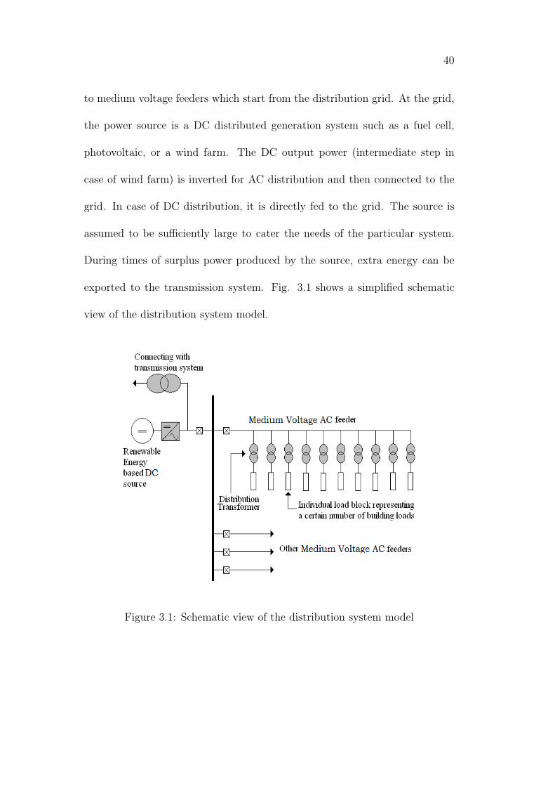
During times of surplus power produced by the source, extra energy can be
exported to the transmission system. Fig. 3.1 shows a simplified schematic
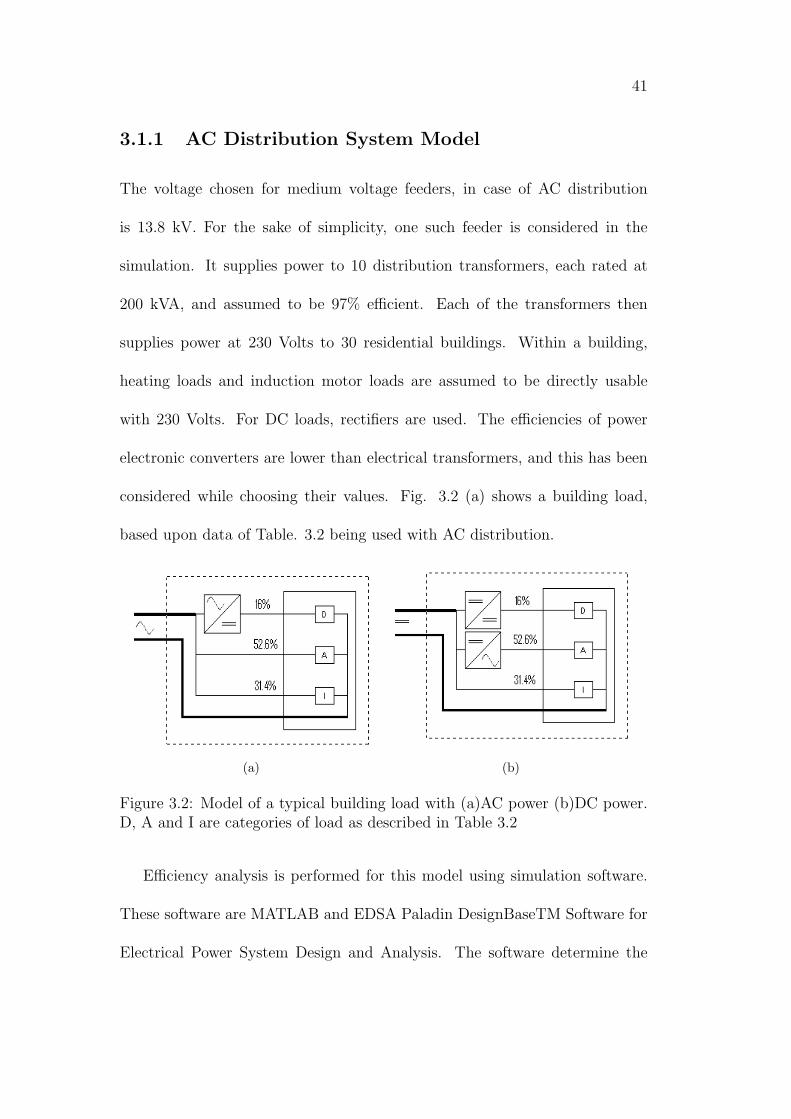
view of the distribution system model.
Figure 3.1: Schematic view of the distribution system model
41
3.1.1 AC Distribution System Model
The voltage chosen for medium voltage feeders, in case of AC distribution
is 13.8 kV. For the sake of simplicity, one such feeder is considered in the
simulation. It supplies power to 10 distribution transformers, each rated at
200 kVA, and assumed to be 97% efficient. Each of the transformers then
supplies power at 230 Volts to 30 residential buildings. Within a building,
heating loads and induction motor loads are assumed to be directly usable
with 230 Volts. For DC loads, rectifiers are used. The efficiencies of power
electronic converters are lower than electrical transformers, and this has been
considered while choosing their values. Fig. 3.2 (a) shows a building load,
based upon data of Table. 3.2 being used with AC distribution.
(a) (b)
Figure 3.2: Model of a typical building load with (a)AC power (b)DC power.D, A and I are categories of load as described in Table 3.2
Efficiency analysis is performed for this model using simulation software.
These software are MATLAB and EDSA Paladin DesignBaseTM Software for
Electrical Power System Design and Analysis. The software determine the
42
input power of the system. The total load power is the same for both AC and
DC systems. This power may be expressed as equation (3.1).
𝑃𝑡𝑜𝑡𝑎𝑙−𝑙𝑜𝑎𝑑𝑖𝑛𝑔 = 𝑛𝐷 ∗ 𝑛𝐵 ∗ 𝐿𝑝𝐵; (3.1)
where 𝑛𝐷 represents number of distribuiton level transformers (or DC/DC
converters in case of DC power distribuiton) in the system, 𝑛𝐵 stands for
number of buildings served by one transformer (or DC/DC converter) and
𝐿𝑝𝐵 represents total load per building. Putting the corresponding values in
equation (3.1) yields
𝑃𝑡𝑜𝑡𝑎𝑙−𝑙𝑜𝑎𝑑𝑖𝑛𝑔 = 10 ∗ 30 ∗ 15 = 1500 𝑘𝑊 (3.2)
With the help of software simulation, the total input power of the AC
system is determined to be 1757.8 kW. Efficiency of the system is calculated
in equation (3.3).
𝜂 =𝑃𝑜𝑢𝑡𝑝𝑢𝑡
𝑃𝑖𝑛𝑝𝑢𝑡
∗ 100 =𝑃𝑡𝑜𝑡𝑎𝑙−𝑙𝑜𝑎𝑑𝑖𝑛𝑔
𝑃𝑡𝑜𝑡𝑎𝑙−𝑖𝑛𝑝𝑢𝑡
∗ 100 =1500
1757.8∗ 100 = 85.33% (3.3)
3.1.2 DC Distribution System Model
In order to find out the possible advantages of DC over AC, while using the DC
output of distributed generation source directly, the same system is used as pre-
viously used for AC, assuming that its insulation can handle the peak voltage
of AC system continuously. The loads are the same, with the only modification
that suitable power electronic converters are employed where required. The

43
peak voltage value of the AC system is chosen as DC line-to-ground voltage.
𝑉𝑑𝑐−𝑙𝑔−𝑝𝑒𝑎𝑘 = 𝑉𝑎𝑐−𝑙𝑔−𝑝𝑒𝑎𝑘 = 𝑉𝑎𝑐−𝑙𝑔−𝑟𝑚𝑠 ∗√2 (3.4)
𝑉𝑑𝑐−𝑙𝑙 = 2 ∗ 𝑉𝑑𝑐−𝑙𝑔−𝑝𝑒𝑎𝑘 (3.5)
The line to line DC voltage comes out to be 22 kV as a result. In place
of distribution transformer a DC/DC converter is used. This converter sup-
plies power to the buildings at 325 Volts (peak value of 230 Volts r.m.s being
used in the AC system). For the in-building distribution, DC/DC and DC/AC
converters are used for DC and AC loads respectively. The heating loads are
assumed to be usable with DC with no modification requirement. At this
point, a possibility exists of using three voltage levels for the in-building DC
distribution as used in [6], because it would eliminate the low efficiency DC/DC
converters for individual devices and replace them with one large, better ef-
ficiency converter. But, since this research aims to explore the prospects of
using the same system for DC as used by AC, therefore minimum modification
should be allowed to the system. Hence the wiring system within the build-
ing is not modified. Fig. 3.2(b) shows the building load being used with DC
distribution. The total power input in the system is found out in the same
manner as before, and efficiency is calculated to be 87.8%.
44
3.2 Results
Efficiencies of both AC and DC distribution systems; as determined in the
previous sections, are compared and the DC system is found to be slightly
more efficient than the AC counterpart. The DC system showed an efficiency
of 87.8% as compared to 85.3% efficiency of the AC system. This can be at-
tributed to no reactive currents flowing in the system, preventing the inversion
stage of source DC power which occurs in case of the AC distribution system,
and higher r.m.s voltage in case of DC system.
Despite the fact that the results show minor improvement in case of DC
distribution which is again prone to variation from case to case; they are,
nevertheless strong enough to point out the potential of DC for being used
in distribution systems with local DC power generation. It should not be
forgotten that DC distribution was the paradigm given up at one stage in
favor of its AC equivalent, and now, the very idea that it can be comparable in
efficiency to an AC distribution system can be strong enough to spark testing of
these systems on practical basis. Furthermore, keeping in mind that this work
has used the same system for DC distribution as previously being employed for
AC system, these results can allow a smooth introduction of DC distribution in
the current power system. However, further work in system protection might
be required for actual implementation of this concept. The assumption of DC
system working at a voltage which was the peak of the AC system voltage,
45
may be required to be tested for a system.
3.2.1 Comment on Results
Despite the fact that the results show an advantage of the new concept of
DC distribution, nevertheless these results are based upon certain assump-
tions. The most important of which is the values used for efficiencies of power
electronic converters employed in the system. This, in particular, has been
the case with a number of past papers [5], [7], [8] also, which used assumed
values of converter efficiencies. These values often tend to be too high to be
achievable for practical and economical reasons. Therefore the overall results
of the research work become doubtful from a practical and economical point
of view. A brief review of past papers shows that, DC is proved to be superior
to AC in reference [5], for in-house distribution with a local DC generation,
with converter efficiencies assumed to be 97.5%. The authors of reference [7]
again show DC to be better than AC for low and medium voltage distribution
but this effect is only observed at converter efficiencies of 99.5%. Similarly in
reference [8] , the authors conclude that DC system does become better than
AC if losses in semiconductor devices are reduced by half. This research work
has assumed efficiency value of (95%) for power electronic converters.
Towards the bold steps of replacing the currently prevailing AC system
with DC or choosing DC instead of AC for the newer locations, there is a need
to specify the minimum required efficiency of converters, and DC systems can
46
be practically implemented only, if and when these minimum required values
are achievable within the framework of economical and practical restraints.
The subsequent section presents a technique that allows finding out the
minimum value of efficiency of power electronic converters to be employed in
the DC system, which will make the DC system at least equally efficient as the
counterpart AC system. If any values of efficiency higher than this calculated
value are used, it will add to the advantage of the DC system.
3.3 Minimum Required Efficiency for Power
Electronic Converters in DC Distribution
System
This section briefly presents the steps leading to the formulation of a technique
to calculate minimum required efficiency of power electronic converters in a
DC distribution system which will make the system equivalent in efficiency
to any given AC distribution system. A top-down approach is followed for
the derivation of this technique i.e. calculations are started from the total
input power of the system from the DC source, and are proceeded towards the
lowest level of loads which are the individual categories of loads in residential
buildings as listed in Table 3.2.
3.3.1 Step 1
This step aims to find out 𝑃𝐼𝐷𝑋 , which is the power input of individual distri-
bution level DC/DC converters in the DC distribution system using 𝑃𝑖𝑛 which
47
is the total power that will be taken in by the system. The value of 𝑃𝑖𝑛 will
be the same as for the AC distribution system since DC system has to match
overall efficiency with the AC system while powering the same loads. 𝑃𝑖𝑛 can
be expressed in an equation form as
𝑃𝑖𝑛 = 𝛽.𝑃𝐼𝐷𝑋 + 𝑙𝑖𝑛𝑒 𝑙𝑜𝑠𝑠𝑒𝑠 1 (3.6)
where 𝛽 is the number of distribution level DC/DC converters in the distri-
bution system and the term 𝑙𝑖𝑛𝑒 𝑙𝑜𝑠𝑠𝑒𝑠 1 refers to the losses taking place in
the distribution feeders transporting power from the bulk power source to the
distribution level converters. For obtaining the value of 𝑃𝐼𝐷𝑋 , an iterative
process is employed. To begin the iterative process a seed value is required for
𝑃𝐼𝐷𝑋 and to find out this value, the expression for 𝑃𝐼𝐷𝑋 is considered.
𝑃𝐼𝐷𝑋 =(𝛼.𝑃𝑏 + 𝑙𝑖𝑛𝑒 𝑙𝑜𝑠𝑠𝑒𝑠 2)
𝜂𝐷𝑋
(3.7)
where 𝛼 is the number of residential buildings served by one distribution level
DC/DC converter, 𝜂𝐷𝑋 is the efficiency of the converter, 𝑃𝑏 is the power input
in one building and the term 𝑙𝑖𝑛𝑒 𝑙𝑜𝑠𝑠𝑒𝑠 2 refers to the losses taking place in
the power conductors running from a distribution converter to the associated
buildings. It can be concluded that
𝑃𝐼𝐷𝑋 > 𝛼.𝑃𝑏 > 𝛼.(𝑃𝐼 + 𝑃𝐴 + 𝑃𝐷) (3.8)
where 𝑃𝐼 , 𝑃𝐴 and 𝑃𝐷 represent power requirements of the three categories
as listed in Table 3.2. The first part of expression (3.8) is concluded from
48
equation (3.7) while the second part arises from the fact that total power
input of a building is greater than the total power used by the loads because
of losses taking place in household power electronic converters. Expression
(3.8) allows to choose a suitable value for 𝑃𝐼𝐷𝑋 by assuming it to be slightly
higher (say 5%) than 𝛼.(𝑃𝐼 +𝑃𝐴+𝑃𝐷). Once this value of 𝑃𝐼𝐷𝑋 is calculated,
the iterative process solves for voltage and current values at each distribution
level converter, starting from the source side. When the far end is reached,
the following equality is tested,
𝑉𝑐𝑎𝑙𝑐𝑢𝑙𝑎𝑡𝑒𝑑 ∗ 𝐼𝑐𝑎𝑙𝑐𝑢𝑙𝑎𝑡𝑒𝑑 = 𝑃𝐼𝐷𝑋−𝑎𝑠𝑠𝑢𝑚𝑒𝑑 (3.9)
If the equality holds, then the value of 𝑃𝐼𝐷𝑋 assumed is the actual value
for the system. Otherwise, iteration is performed again with a modified value
of 𝑃𝐼𝐷𝑋 . The modification depends upon the results of the previous iteration.
Specifically, if
𝑉𝑐𝑎𝑙𝑐𝑢𝑙𝑎𝑡𝑒𝑑 ∗ 𝐼𝑐𝑎𝑙𝑐𝑢𝑙𝑎𝑡𝑒𝑑 < 𝑃𝐼𝐷𝑋−𝑎𝑠𝑠𝑢𝑚𝑒𝑑 (3.10)
then assumed value of 𝑃𝐼𝐷𝑋 is slightly reduced for the next iteration and vice
versa. A software program may be designed for this step, and the iterations
may be terminated when product of voltage and current for the last distribu-
tion level converter is suitably close to assumed value of 𝑃𝐼𝐷𝑋 .
3.3.2 Step 2
In the second step, the previously obtained 𝑃𝐼𝐷𝑋 is related to 𝜂𝑃𝐸𝐶 which is
the efficiency of power electronic converters used in home appliances of the
49
buildings. Equation (3.7) is the starting point for this step. The line losses in
this expression can be easily expressed as 𝐼2𝑅 losses with
𝐼 =𝑃𝑏
𝑉𝑏
(3.11)
𝑅 = 𝑟1 ∗ 𝑙1 (3.12)
where 𝑉𝑏 is voltage at each housing unit and 𝑟1 and 𝑙1 are resistance and length
of power conductors from distribution converter to individual buildings. The
term 𝑃𝑏 which symbolizes the power input in one building can be expressed as
𝑃𝑏 = 𝑃𝐼 +𝑃𝐴 + 𝑃𝐷
𝜂𝑃𝐸𝐶
(3.13)
Substituting expressions of 𝑃𝑏 and 𝑙𝑖𝑛𝑒 𝑙𝑜𝑠𝑠𝑒𝑠 2 in equation (3.7), and choos-
ing a suitable value for 𝜂𝐷𝑋 , the resultant can be simplified to produce the
following equation
𝑃𝐼𝐷𝑋 = 𝑎.𝜂−2𝑃𝐸𝐶 + 𝑏.𝜂−1
𝑃𝐸𝐶 + 𝑐 (3.14)
where,
𝑎 =𝑟1.𝑙1 ∗ (𝑃𝐴 + 𝑃𝐷)
2
𝑉 2𝑏
∗ 𝛼
𝜂𝐷𝑋
(3.15)
𝑏 =
[(𝑃𝐴 + 𝑃𝐷) +
2𝑃𝐼(𝑃𝐴 + 𝑃𝐷)
𝑉 2𝑏
]∗ 𝛼
𝜂𝐷𝑋
(3.16)
𝑐 =
[𝑃𝐼 +
𝑃 2𝐼
𝑉 2𝑏
∗ 𝑟1𝑙1]]∗ 𝛼
𝜂𝐷𝑋
(3.17)
Equation (3.14) can be further simplified as
𝑎′.𝜂−2𝑃𝐸𝐶 + 𝑏′.𝜂−1
𝑃𝐸𝐶 + 𝑐′ = 0 (3.18)
50
where 𝑎′ and 𝑏′ are the same as 𝑎 and 𝑏 while
𝑐′ =[𝑃𝐼 +
𝑃 2𝐼
𝑉 2𝑏
∗ 𝑟1𝑙1]]∗ 𝛼
𝜂𝐷𝑋
− 𝑃𝐼𝐷𝑋 (3.19)
Numerical analysis techniques such as bisection method may be applied
to solve equation (3.18); or alternately 1/𝜂𝑃𝐸𝐶 may be replaced by a dummy
variable ‘𝑥 which converts this equation to a quadratic equation as given in
equation 3.20.
𝑎′.𝑥2 + 𝑏′.𝑥+ 𝑐′ = 0 (3.20)
This can be solved by quadratic equation formula to find x, and then 𝜂𝑃𝐸𝐶
can be calculated. The resultant value of 𝜂𝑃𝐸𝐶 is the minimum efficiency re-
quired to make DC system at least as efficient as the AC system. If higher
values for 𝜂𝑃𝐸𝐶 are chosen, higher efficiency can be achieved for the DC distri-
bution system. It is noteworthy that the above technique allows comparison of
DC and AC distribution systems with or without incorporation of renewable
energy generation which is DC in nature. This is because the starting point
of this technique is the efficiency of the AC system required to be replaced,
and there is no restriction of power source being originally DC. Hence this
technique may be used to find out prospects of replacing any conventional AC
distribution system with a DC counterpart.

51
3.4 Case Study
A case study is presented in this Section which serves both as a demonstra-
tion of the previously derived technique and as a verification for it. The AC
distribution system presented earlier, whose overall efficiency was reported in
Section 3.2 to be 85.3%, is considered for the case study. The goal is to find out
the efficiency of power electronic converters to be used in residential buildings,
if the same system employs DC distribution and the overall system efficiency
remains the same i.e. 85.3%.
Step 1 of the technique is executed and the iterations are performed by
MATLAB code. After a certain number of iterations, the product of 𝑉𝑐𝑎𝑙𝑐𝑢𝑙𝑎𝑡𝑒𝑑
and 𝐼𝑐𝑎𝑙𝑐𝑢𝑙𝑎𝑡𝑒𝑑 is 173.37 kW while the value for 𝑃𝐼𝐷𝑋−𝑎𝑠𝑠𝑢𝑚𝑒𝑑 is 173.30 kW.
Since these values are fairly close, so this assumed value of 𝑃𝐼𝐷𝑋 is taken
to be the actual value for the system. In the next step i.e. step 2 of the
technique, the previously calculated value of 𝑃𝐼𝐷𝑋 is used for the calculations
of coefficients 𝑎′, 𝑏′ and 𝑐′ of equation (3.18). The values of various quantities
in the expressions for these coefficients are taken to be the same as in the
case of AC distribution system. The only exceptions are the values of 𝑉𝑏 and
𝜂𝐷𝑋 which are taken to be 325 Volts and 95% respectively. Lastly, numerical
analysis is used to solve equation (3.18) and 𝜂𝑃𝐸𝐶 is calculated to be 89.55%.
This is the required value of efficiency of power electronic converters to be
used in household appliances which will make the DC system equally efficient
52
as the AC counterpart. To verify the technique, the above achieved value of
𝜂𝑃𝐸𝐶 was used for the simulation of DC system just as the system of section
3.1.2, and efficiency of the DC system was calculated in the same way to be
85.37%. This value is approximately equal to the efficiency (85.3%) of the AC
system to be replaced by DC distribution. Hence the technique was verified.
3.5 Summary
In this Chapter an efficiency comparison was made between DC and AC dis-
tribution systems. For the assumed conditions, it was observed that the DC
paradigm is better in efficiency than its AC rival. Furthermore, in this respect,
a mathematical technique was presented which allows to find out the minimum
required efficiency of power electronic converters in a DC distribution system
that can make this system at least as efficient as an AC counterpart.
Having presented DC as an option for power distribution, this research
shifts focus towards the stability issue of a DC DPS. As mentioned earlier,
the DC DPS may be a potential future DC power distribution system. The
following chapters present a control technique that can lead to the stability
of a single buck DC/DC converter loaded with a constant power load while
working in open loop. Eventually this technique will be used to simulated a
larger DC DPS towards the end of this thesis.
Chapter 4
Hybrid of Voltage and CurrentMode Control Technique
(Some of the content in this chapter has been submitted for publication in In-
ternational Journal of Engineering, Science and Technology, 2011 [51]). This
chapter presents a current-limiting idea based control technique which can al-
low a buck converter loaded by a constant power load to operate in open loop in
continuous conduction mode without becoming unstable. Traditionally, such a
system has been considered to be unstable (as discussed in Chapter 2). Trans-
fer functions have been developed for this system in continuous conduction
mode (CCM) and discontinuous conduction mode (DCM) and it is stated to
be unstable in CCM with either current mode control (CMC) or voltage mode
control (VMC).
However, an actual buck converter system loaded with a constant power
load (CPL) will always shift to DCM (in case of system oscillations) even if it
begins operation in CCM. This is because any voltage and current perturba-
tions start to get magnified because of negative impedance behavior of CPL,
53
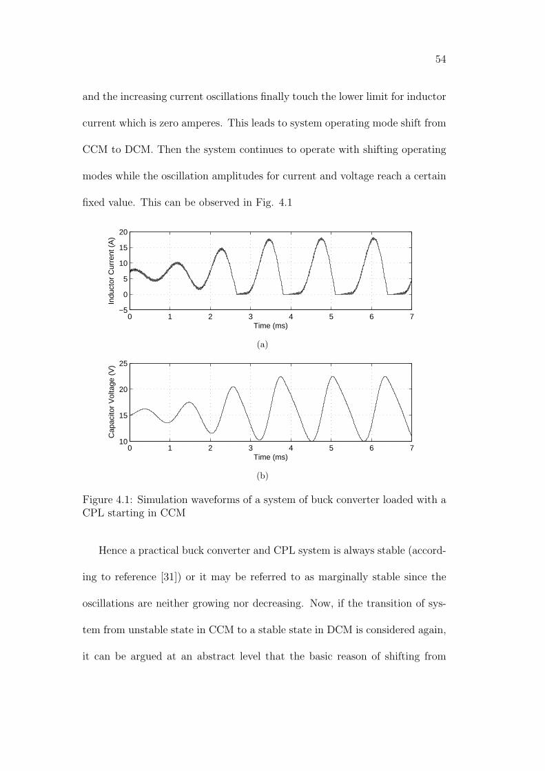
54
and the increasing current oscillations finally touch the lower limit for inductor
current which is zero amperes. This leads to system operating mode shift from
CCM to DCM. Then the system continues to operate with shifting operating
modes while the oscillation amplitudes for current and voltage reach a certain
fixed value. This can be observed in Fig. 4.1
0 1 2 3 4 5 6 7−5
0
5
10
15
20
Time (ms)
Indu
ctor
Cur
rent
(A
)
(a)
0 1 2 3 4 5 6 710
15
20
25
Time (ms)
Cap
acito
r V
olta
ge (
V)
(b)
Figure 4.1: Simulation waveforms of a system of buck converter loaded with aCPL starting in CCM
Hence a practical buck converter and CPL system is always stable (accord-
ing to reference [31]) or it may be referred to as marginally stable since the
oscillations are neither growing nor decreasing. Now, if the transition of sys-
tem from unstable state in CCM to a stable state in DCM is considered again,
it can be argued at an abstract level that the basic reason of shifting from

55
instability to marginal stability was putting a check or limit on 𝑖𝐿. Not only
does this limit prevent 𝑖𝐿 from going below a certain value (i.e. zero amperes),
but it also eventually stops the increase in peak values of 𝑣𝐶 and 𝑖𝐿, as can be
seen from Fig. 4.1.
So, this limit, although for the lower peak value of 𝑖𝐿, serves to put a check
on the upper peak of 𝑖𝐿 as well. Based upon this idea, it can be argued, that
what if there could be a limit on the upper peak value which would put a check
on lower peaks of 𝑖𝐿? If such a limit can be introduced in the system then
it might be stable or marginally stable in continuous conduction mode, if the
lower peak is totally avoided. In other words, what if there is a limit on upper
peak values of 𝑖𝐿 which can keep the system from being unstable as well as
keep it in continuous conduction mode? This is an abstract discussion for the
basic principle of the control technique (named HVC - Hybrid of Voltage and
Current mode control) presented in this chapter which is based on the idea of
current limiting. In this control technique, an upper limit is specified for 𝑖𝐿.
When the oscillating inductor current reaches this value; it stays close to it
for a brief period of time, then sweeps down but only for a small excursion,
coming back to the peak value again. As a result, the current oscillations
are kept under control and system is withheld from becoming unstable and it
continues to operate in continuous conduction mode.
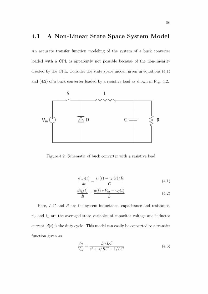
56
4.1 A Non-Linear State Space System Model
An accurate transfer function modeling of the system of a buck converter
loaded with a CPL is apparently not possible because of the non-linearity
created by the CPL. Consider the state space model, given in equations (4.1)
and (4.2) of a buck converter loaded by a resistive load as shown in Fig. 4.2.
Figure 4.2: Schematic of buck converter with a resistive load
𝑑𝑣𝐶(𝑡)
𝑑𝑡=
𝑖𝐿(𝑡)− 𝑣𝐶(𝑡)/𝑅
𝐶(4.1)
𝑑𝑖𝐿(𝑡)
𝑑𝑡=
𝑑(𝑡) ∗ 𝑉𝑖𝑛 − 𝑣𝐶(𝑡)
𝐿(4.2)
Here, 𝐿,𝐶 and 𝑅 are the system inductance, capacitance and resistance,
𝑣𝐶 and 𝑖𝐿 are the averaged state variables of capacitor voltage and inductor
current, 𝑑(𝑡) is the duty cycle. This model can easily be converted to a transfer
function given as
𝑉𝐶
𝑉𝑖𝑛
=𝐷/𝐿𝐶
𝑠2 + 𝑠/𝑅𝐶 + 1/𝐿𝐶(4.3)
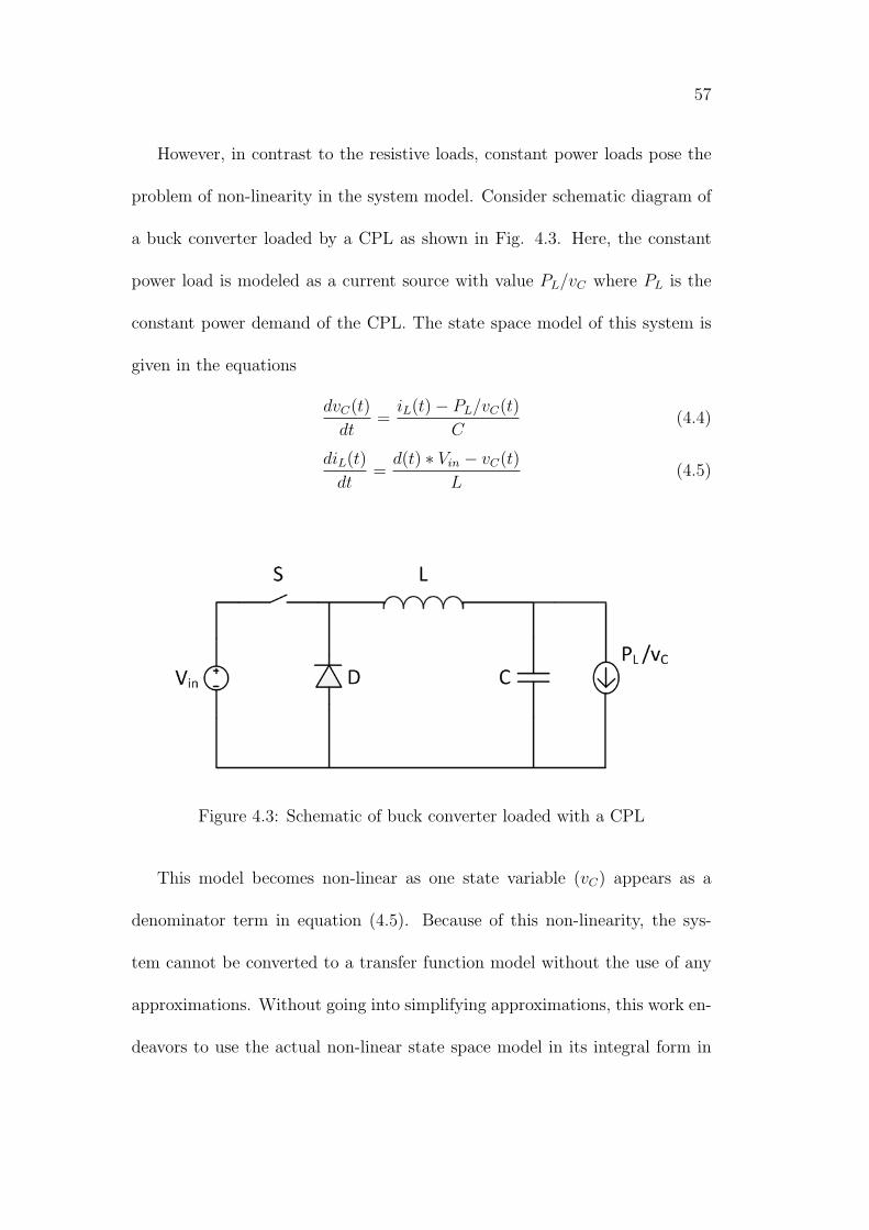
57
However, in contrast to the resistive loads, constant power loads pose the
problem of non-linearity in the system model. Consider schematic diagram of
a buck converter loaded by a CPL as shown in Fig. 4.3. Here, the constant
power load is modeled as a current source with value 𝑃𝐿/𝑣𝐶 where 𝑃𝐿 is the
constant power demand of the CPL. The state space model of this system is
given in the equations
𝑑𝑣𝐶(𝑡)
𝑑𝑡=
𝑖𝐿(𝑡)− 𝑃𝐿/𝑣𝐶(𝑡)
𝐶(4.4)
𝑑𝑖𝐿(𝑡)
𝑑𝑡=
𝑑(𝑡) ∗ 𝑉𝑖𝑛 − 𝑣𝐶(𝑡)
𝐿(4.5)
Figure 4.3: Schematic of buck converter loaded with a CPL
This model becomes non-linear as one state variable (𝑣𝐶) appears as a
denominator term in equation (4.5). Because of this non-linearity, the sys-
tem cannot be converted to a transfer function model without the use of any
approximations. Without going into simplifying approximations, this work en-
deavors to use the actual non-linear state space model in its integral form in
58
a mathematical model. The integral form of the non-linear model is given by
the equations
𝑣𝐶(𝑡) =1
𝐶
∫[𝑖𝐿(𝑡)− 𝑃𝐿/𝑣𝐶(𝑡)] 𝑑(𝑡) (4.6)
𝑖𝐿(𝑡) =1
𝐿
∫[𝑑(𝑡) ∗ 𝑉𝑖𝑛 − 𝑣𝐶(𝑡)] 𝑑(𝑡) (4.7)
This non-linear model is applicable for CCM as well as DCM modes of system
operation. It also allows to have an explicit control on the variable for inductor
current and hence it can be limited to an upper maximum. This allows the
realization of HVC control.
Besides this model, the circuit based switched model is also used. MAT-
LAB/SIMULINK environment is used for the simulation of these models as
well as for closed loop system controller design as presented in Chapter 7.
4.2 HVC Control Technique
This section presents details of HVC control. Voltage mode control of a buck
converter is based on directly controlling duty cycle of the input switching
waveform to control the output voltage. On the other hand, current mode
control attempts to control the current in the switch S (as shown in Fig. 4.3)
or the system inductor and turns the switch off when current has reached
an upper bound as specified by the controller. However neither of these two
paradigms can avoid instability in the system, however, HVC control allows
system operation without becoming unstable.
To start with, a mathematical proof of keeping system from instability is
59
provided. This is based on simulation of non-linear mathematical model of the
system. The simulations of circuit based switched model are presented later
in this Chapter in Section 4.4.
4.2.1 HVC Control - Mathematical Proof
A mathematical proof of this theory is obtained from the simulation of integral
form of the averaged state space model of the system as given in equations (4.6)
and (4.7), with a specific peak limit for inductor current. This model, however,
cannot represent system switching ripple, and that is shown in the circuit based
simulation. Converter system I, as presented in Table A.1 in Appendix A, is
used for this simulation of the system. The expression of duty cycle (𝐷) for
buck converter
𝐷 =𝑉𝑜𝑢𝑡𝑝𝑢𝑡
𝑉𝑖𝑛𝑝𝑢𝑡
(4.8)
dictates that this value be set at 0.75. This system is simulated, starting from
CCM mode, where it is unstable hence it shifts to its stable state in DCM
with large value of peak inductor current and unacceptable ripple in output
voltage. The simulation waveforms for capacitor voltage and inductor current
are shown in Fig. 4.4.
Now, the idea of HVC control, as mentioned earlier is to introduce an
upper peak limit in this system, such that it can remove the requirement of
the lower limit and lift the lower peak of 𝑖𝐿 from its value of zero amperes in
DCM to a value higher than this, so that the system is effectively in CCM.
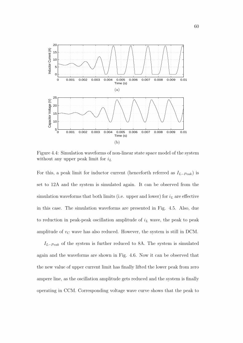
60
0 0.001 0.002 0.003 0.004 0.005 0.006 0.007 0.008 0.009 0.01
0
5
10
15
20
Time (s)
Indu
ctor
Cur
rent
(A)
(a)
0 0.001 0.002 0.003 0.004 0.005 0.006 0.007 0.008 0.009 0.015
10
15
20
25
Time (s)
Cap
acito
r Vol
tage
(V)
(b)
Figure 4.4: Simulation waveforms of non-linear state space model of the systemwithout any upper peak limit for 𝑖𝐿
For this, a peak limit for inductor current (henceforth referred as 𝐼𝐿−𝑃𝑒𝑎𝑘) is
set to 12A and the system is simulated again. It can be observed from the
simulation waveforms that both limits (i.e. upper and lower) for 𝑖𝐿 are effective
in this case. The simulation waveforms are presented in Fig. 4.5. Also, due
to reduction in peak-peak oscillation amplitude of 𝑖𝐿 wave, the peak to peak
amplitude of 𝑣𝐶 wave has also reduced. However, the system is still in DCM.
𝐼𝐿−𝑃𝑒𝑎𝑘 of the system is further reduced to 8A. The system is simulated
again and the waveforms are shown in Fig. 4.6. Now it can be observed that
the new value of upper current limit has finally lifted the lower peak from zero
ampere line, as the oscillation amplitude gets reduced and the system is finally
operating in CCM. Corresponding voltage wave curve shows that the peak to
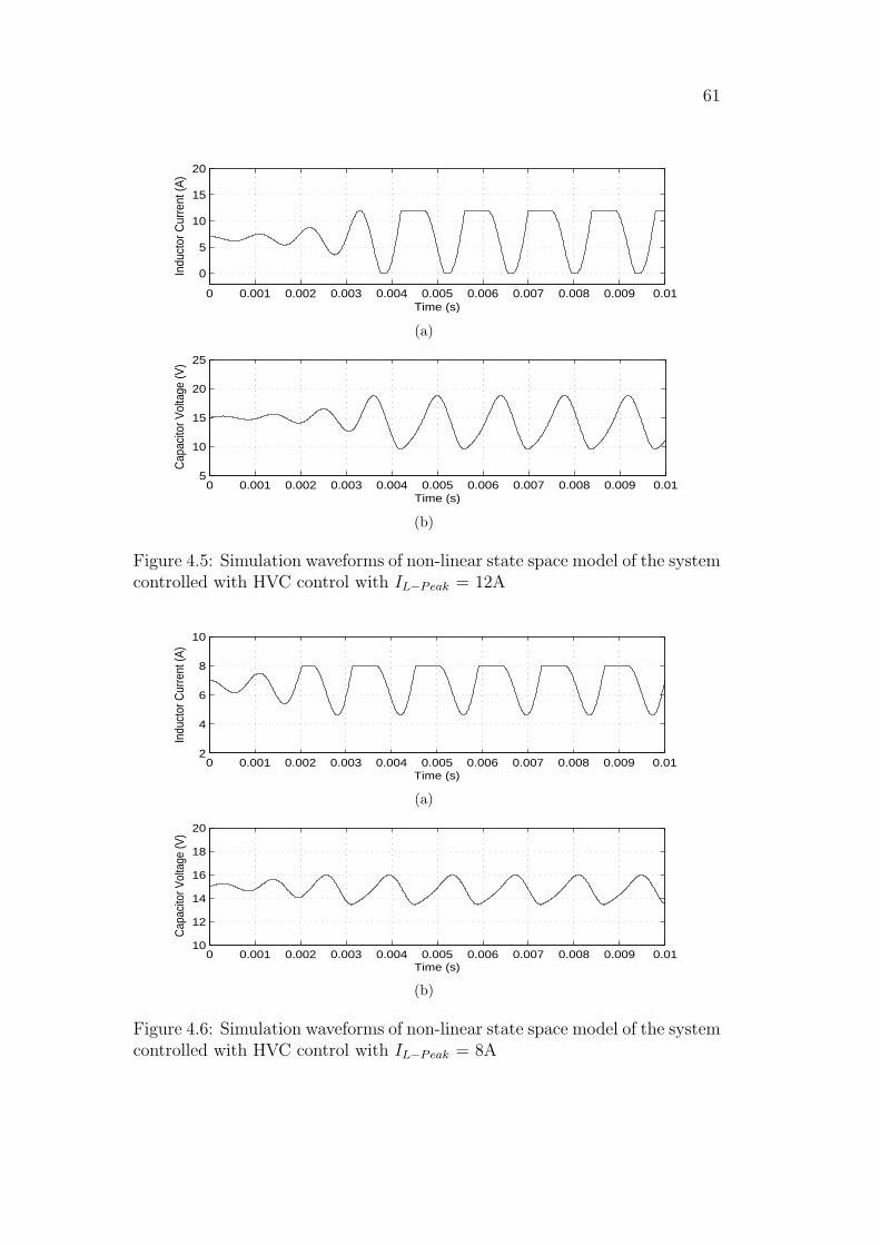
61
0 0.001 0.002 0.003 0.004 0.005 0.006 0.007 0.008 0.009 0.01
0
5
10
15
20
Time (s)
Indu
ctor
Cur
rent
(A)
(a)
0 0.001 0.002 0.003 0.004 0.005 0.006 0.007 0.008 0.009 0.015
10
15
20
25
Time (s)
Cap
acito
r Vol
tage
(V)
(b)
Figure 4.5: Simulation waveforms of non-linear state space model of the systemcontrolled with HVC control with 𝐼𝐿−𝑃𝑒𝑎𝑘 = 12A
0 0.001 0.002 0.003 0.004 0.005 0.006 0.007 0.008 0.009 0.012
4
6
8
10
Time (s)
Indu
ctor
Cur
rent
(A)
(a)
0 0.001 0.002 0.003 0.004 0.005 0.006 0.007 0.008 0.009 0.0110
12
14
16
18
20
Time (s)
Cap
acito
r Vol
tage
(V)
(b)
Figure 4.6: Simulation waveforms of non-linear state space model of the systemcontrolled with HVC control with 𝐼𝐿−𝑃𝑒𝑎𝑘 = 8A
62
peak ripple has reduced as well.
4.2.2 Lower Limit of 𝐼𝐿−𝑃𝑒𝑎𝑘
Theoretically, under appropriate start up, the lower limit of 𝐼𝐿−𝑃𝑒𝑎𝑘 can be
reduced to even smaller values as compared to those used in the previous
subsection. This theoretical lower limit will be the nominal value of 𝑖𝐿 which
can be expressed as
𝐼𝐿−𝑛𝑜𝑚𝑖𝑛𝑎𝑙 =𝑃𝐿
𝑉𝐶−𝑛𝑜𝑚𝑖𝑛𝑎𝑙
(4.9)
where 𝑉𝐶−𝑛𝑜𝑚𝑖𝑛𝑎𝑙 is actually the desired output voltage and hence equal to
𝑉𝑜𝑢𝑡𝑝𝑢𝑡.
Hence a system simulation with 𝐼𝐿−𝑃𝑒𝑎𝑘 very close to this value will show
almost zero oscillation amplitude for 𝑣𝐶 and 𝑖𝐿. However, an actual buck
converter and CPL system has a certain value of peak to peak switching ripple
present in 𝑖𝐿 wave which is not represented by the averaged system model, and
the actual system cannot work with such a low value of 𝐼𝐿−𝑃𝑒𝑎𝑘.
4.2.3 Shifting between Voltage and Current Mode Con-trols
In the averaged non-linear modeling of the system, it remains in current mode
control for the time span where inductor current is equal to 𝐼𝐿−𝑃𝑒𝑎𝑘, and for
the remaining values of 𝑖𝐿, the system remains in duty cycle based control.
Hence, a hybrid of the two control modes enables to allow system operation in
open loop, while neither of the two modes can do so individually.
63
As evident from previous description, in HVC control both duty cycle and
peak current limit are specified to the system. For the switching cycles (of the
actual system or its circuit based simulation) where inductor current remains
less than the specified peak limit, duty cycle controls the turn-on and turn-off
of the switch. The system remains in voltage mode control. However, when the
current increases and attempts to violate the peak current limit of the system,
the switch is turned off and the system remains in current mode control with
turn on at clock time, for as long as inductor current keeps on reaching peak
limit in the switching cycles. Once inductor current peak (due to switching
ripple) becomes less than the peak limit, the system returns to normal duty
cycle based control.
With this mixing of current mode control and voltage mode control, the
system of buck converter loaded with a constant power load is allowed to be
operated in continuous conduction mode while in an open loop.
4.3 Implementation of Controller for HVC Con-
trol Technique
A controller needs to be designed for the circuit based simulation of the system
of a buck converter loaded by a CPL and controlled by HVC control. This is
in contrast to the simulation of averaged system model where the system was
based upon state space equations in integral form, and inductor current could
be limited to a specific peak value by directly specifying a peak limit for the
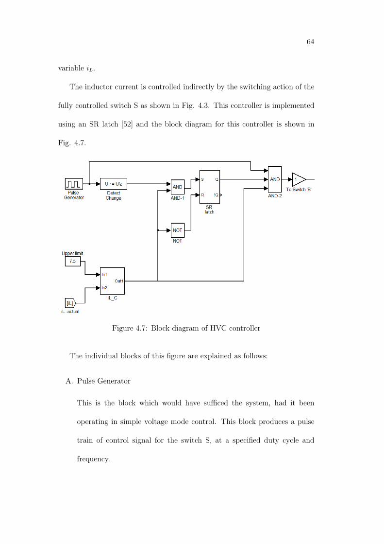
64
variable 𝑖𝐿.
The inductor current is controlled indirectly by the switching action of the
fully controlled switch S as shown in Fig. 4.3. This controller is implemented
using an SR latch [52] and the block diagram for this controller is shown in
Fig. 4.7.
Figure 4.7: Block diagram of HVC controller
The individual blocks of this figure are explained as follows:
A. Pulse Generator
This is the block which would have sufficed the system, had it been
operating in simple voltage mode control. This block produces a pulse
train of control signal for the switch S, at a specified duty cycle and
frequency.

65
B. Detect Change
This block is supposed to detect a change in value of its input signal.
According to its position, this block is meant to produce a single pulse
whenever the pulse generator varies its output.
C. iL C
This block, abbreviated for 𝑖𝐿 condition, takes the actual 𝑖𝐿 and the value
of 𝐼𝐿−𝑃𝑒𝑎𝑘 as input and its output is based upon the following logic.
𝐼𝑓{𝑖𝐿−𝑎𝑐𝑢𝑡𝑎𝑙 ≤ 𝐼𝐿−𝑝𝑒𝑎𝑘}𝑂𝑢𝑡𝑝𝑢𝑡 = 1 (4.10)
𝐼𝑓{𝑖𝐿−𝑎𝑐𝑢𝑡𝑎𝑙 > 𝐼𝐿−𝑝𝑒𝑎𝑘}𝑂𝑢𝑡𝑝𝑢𝑡 = 0 (4.11)
D. SR Latch
The truth table for the SR latch is presented in Table 4.1. The output
signal 𝑄 of this latch is used to prevent any unnecessary turning on of
the switch S, as mentioned subsequently.
Table 4.1: Truth Table of SR LatchS R Q
1 0 1
0 1 0
0 0 𝑄𝑛−1
1 1 X
In simple words, the working of this controller can be summarized in terms
of the switching on and off of the fully controlled switch S. This switch is
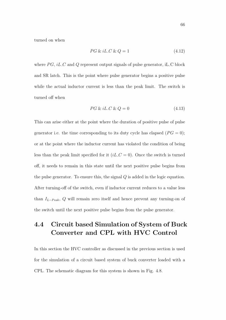
66
turned on when
𝑃𝐺& 𝑖𝐿 𝐶 &𝑄 = 1 (4.12)
where 𝑃𝐺, 𝑖𝐿 𝐶 and 𝑄 represent output signals of pulse generator, iL C block
and SR latch. This is the point where pulse generator begins a positive pulse
while the actual inductor current is less than the peak limit. The switch is
turned off when
𝑃𝐺& 𝑖𝐿 𝐶 &𝑄 = 0 (4.13)
This can arise either at the point where the duration of positive pulse of pulse
generator i.e. the time corresponding to its duty cycle has elapsed (𝑃𝐺 = 0);
or at the point where the inductor current has violated the condition of being
less than the peak limit specified for it (𝑖𝐿 𝐶 = 0). Once the switch is turned
off, it needs to remain in this state until the next positive pulse begins from
the pulse generator. To ensure this, the signal 𝑄 is added in the logic equation.
After turning-off of the switch, even if inductor current reduces to a value less
than 𝐼𝐿−𝑃𝑒𝑎𝑘, 𝑄 will remain zero itself and hence prevent any turning-on of
the switch until the next positive pulse begins from the pulse generator.
4.4 Circuit based Simulation of System of Buck
Converter and CPL with HVC Control
In this section the HVC controller as discussed in the previous section is used
for the simulation of a circuit based system of buck converter loaded with a
CPL. The schematic diagram for this system is shown in Fig. 4.8.
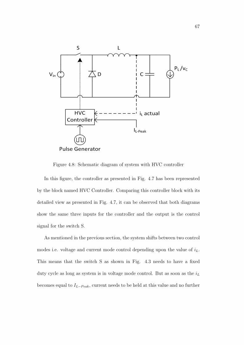
67
Figure 4.8: Schematic diagram of system with HVC controller
In this figure, the controller as presented in Fig. 4.7 has been represented
by the block named HVC Controller. Comparing this controller block with its
detailed view as presented in Fig. 4.7, it can be observed that both diagrams
show the same three inputs for the controller and the output is the control
signal for the switch S.
As mentioned in the previous section, the system shifts between two control
modes i.e. voltage and current mode control depending upon the value of 𝑖𝐿.
This means that the switch S as shown in Fig. 4.3 needs to have a fixed
duty cycle as long as system is in voltage mode control. But as soon as the 𝑖𝐿
becomes equal to 𝐼𝐿−𝑃𝑒𝑎𝑘, current needs to be held at this value and no further

68
increase should be allowed. The averaged system model allowed to perform
these by directly putting a limit on the variable for inductor current i.e. 𝑖𝐿.
However, the switched system cannot keep the current constant at a fixed
value. The instantaneous value of 𝑖𝐿 will either be increasing or decreasing.
So, for switched simulation, the switch S is turned off as soon as 𝑖𝐿 touches
𝐼𝐿−𝑃𝑒𝑎𝑘. The current then falls down as inductor loses its energy and then after
a certain time, the switch is turned on again. Now, if the 𝑖𝐿 reaches 𝐼𝐿−𝑃𝑒𝑎𝑘
again in this cycle, then the switch should be turned off again, similar to the
previous cycle, otherwise, the system duty cycle will dictate the turn off of the
switch.
For the circuit based simulation, the buck converter (of Converter System
I in Table A.1 in Appendix A) is simulated with switching frequency of 10kHz.
In this system, however, 𝐼𝐿−𝑃𝑒𝑎𝑘 of 6.8A (as used in the non-linear mathe-
matical model of the system), cannot be used and the system requires quite a
larger value for the upper current limit. Fig. 4.9(a) shows the inductor cur-
rent waveform of the switched system with 𝐼𝐿−𝑃𝑒𝑎𝑘 of 12A. The corresponding
system voltage is shown in Fig. 4.9(b). It may be observed that this system,
has quiet a high peak to peak ripple value.
The reason for this large deviation from the mathematical model is the high
value of switching ripple in the inductor current. The mathematical model,
being based on averaging of the system, fails to account for the switching
ripple and considers the average value of the inductor current. While a close
69
0 0.001 0.002 0.003 0.004 0.005 0.006 0.007 0.008 0.009 0.010
2
4
6
8
10
12
Time (s)
Indu
ctor
Cur
rent
(A)
(a)
0 0.001 0.002 0.003 0.004 0.005 0.006 0.007 0.008 0.009 0.0110
12
14
16
18
20
Time (s)
Cap
acito
r Vol
tage
(V)
(b)
Figure 4.9: Simulation waveforms of circuit based model of the system con-trolled with HVC control
up of the inductor current waveform reveals the ripple to be close to 2 A. This
high value of peak to peak ripple and thus a deviation from the mathematical
model disallows the use of the same 𝐼𝐿−𝑃𝑒𝑎𝑘 as employed in the averaged model
case. Therefore, the 𝐼𝐿−𝑃𝑒𝑎𝑘 value is required to be increased for the system
to function.
In order to reduce the disparity between the two system models, the switch-
ing frequency of the system is increased to 50kHz and it is simulated again.
This allows the circuit based model to be closer to the averaged model as its
peak to peak current ripple reduces as observable in Fig. 4.10. A reduced
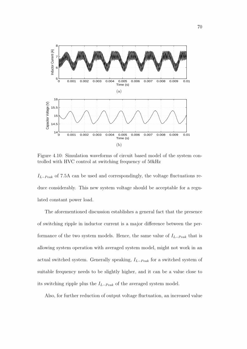
70
0 0.001 0.002 0.003 0.004 0.005 0.006 0.007 0.008 0.009 0.015
6
7
8
Time (s)
Indu
ctor
Cur
rent
(A)
(a)
0 0.001 0.002 0.003 0.004 0.005 0.006 0.007 0.008 0.009 0.0114
14.5
15
15.5
16
Time (s)
Cap
acito
r Vol
tage
(V)
(b)
Figure 4.10: Simulation waveforms of circuit based model of the system con-trolled with HVC control at switching frequency of 50kHz
𝐼𝐿−𝑃𝑒𝑎𝑘 of 7.5A can be used and correspondingly, the voltage fluctuations re-
duce considerably. This new system voltage should be acceptable for a regu-
lated constant power load.
The aforementioned discussion establishes a general fact that the presence
of switching ripple in inductor current is a major difference between the per-
formance of the two system models. Hence, the same value of 𝐼𝐿−𝑃𝑒𝑎𝑘 that is
allowing system operation with averaged system model, might not work in an
actual switched system. Generally speaking, 𝐼𝐿−𝑃𝑒𝑎𝑘 for a switched system of
suitable frequency needs to be slightly higher, and it can be a value close to
its switching ripple plus the 𝐼𝐿−𝑃𝑒𝑎𝑘 of the averaged system model.
Also, for further reduction of output voltage fluctuation, an increased value
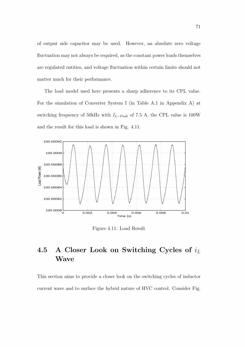
71
of output side capacitor may be used. However, an absolute zero voltage
fluctuation may not always be required, as the constant power loads themselves
are regulated entities, and voltage fluctuation within certain limits should not
matter much for their performance.
The load model used here presents a sharp adherence to its CPL value.
For the simulation of Converter System I (in Table A.1 in Appendix A) at
switching frequency of 50kHz with 𝐼𝐿−𝑃𝑒𝑎𝑘 of 7.5 A, the CPL value is 100W
and the result for this load is shown in Fig. 4.11.
0 0.002 0.004 0.006 0.008 0.01100.0008
100.00082
100.00084
100.00086
100.00088
100.0009
100.00092
Time (s)
Load
Pow
er (W
)
Figure 4.11: Load Result
4.5 A Closer Look on Switching Cycles of 𝑖𝐿Wave
This section aims to provide a closer look on the switching cycles of inductor
current wave and to surface the hybrid nature of HVC control. Consider Fig.
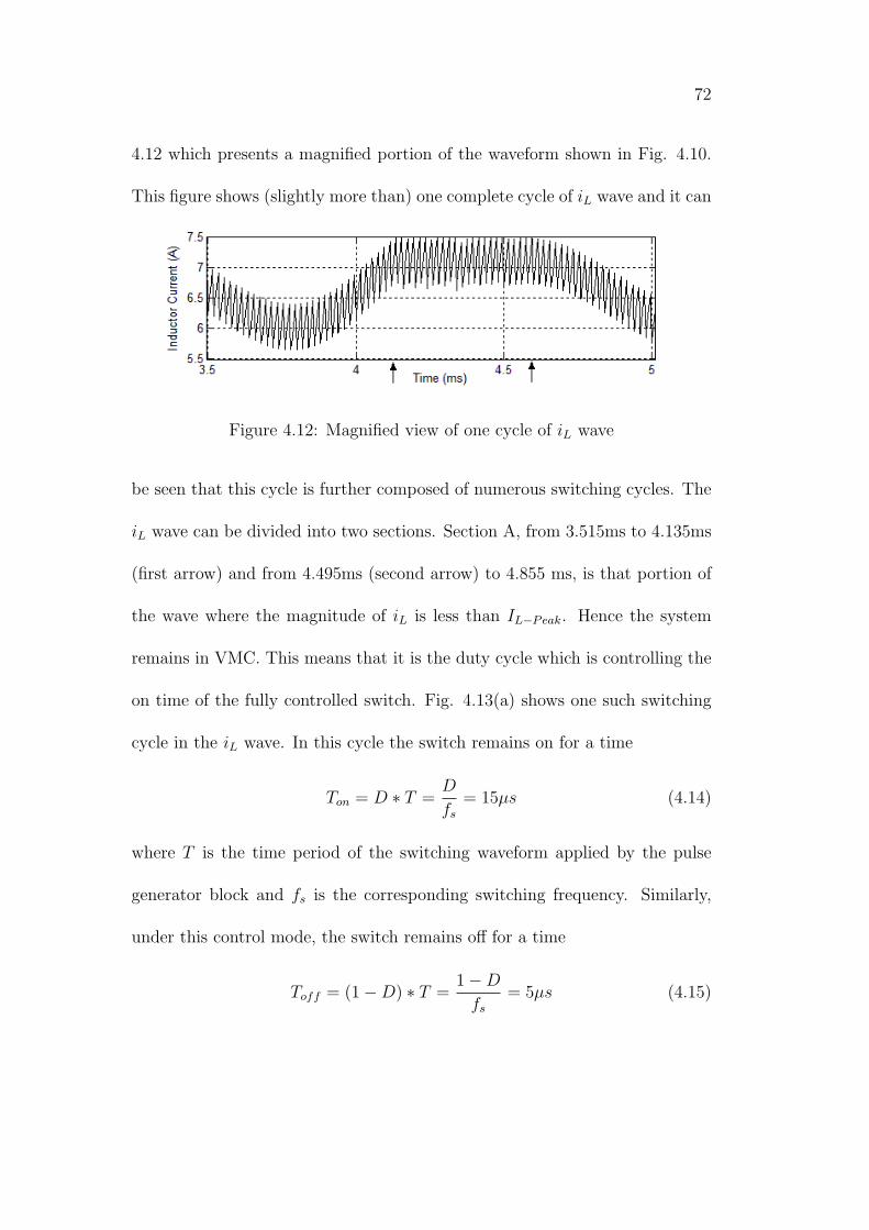
72
4.12 which presents a magnified portion of the waveform shown in Fig. 4.10.
This figure shows (slightly more than) one complete cycle of 𝑖𝐿 wave and it can
Figure 4.12: Magnified view of one cycle of 𝑖𝐿 wave
be seen that this cycle is further composed of numerous switching cycles. The
𝑖𝐿 wave can be divided into two sections. Section A, from 3.515ms to 4.135ms
(first arrow) and from 4.495ms (second arrow) to 4.855 ms, is that portion of
the wave where the magnitude of 𝑖𝐿 is less than 𝐼𝐿−𝑃𝑒𝑎𝑘. Hence the system
remains in VMC. This means that it is the duty cycle which is controlling the
on time of the fully controlled switch. Fig. 4.13(a) shows one such switching
cycle in the 𝑖𝐿 wave. In this cycle the switch remains on for a time
𝑇𝑜𝑛 = 𝐷 ∗ 𝑇 =𝐷
𝑓𝑠= 15𝜇𝑠 (4.14)
where 𝑇 is the time period of the switching waveform applied by the pulse
generator block and 𝑓𝑠 is the corresponding switching frequency. Similarly,
under this control mode, the switch remains off for a time
𝑇𝑜𝑓𝑓 = (1−𝐷) ∗ 𝑇 =1−𝐷
𝑓𝑠= 5𝜇𝑠 (4.15)
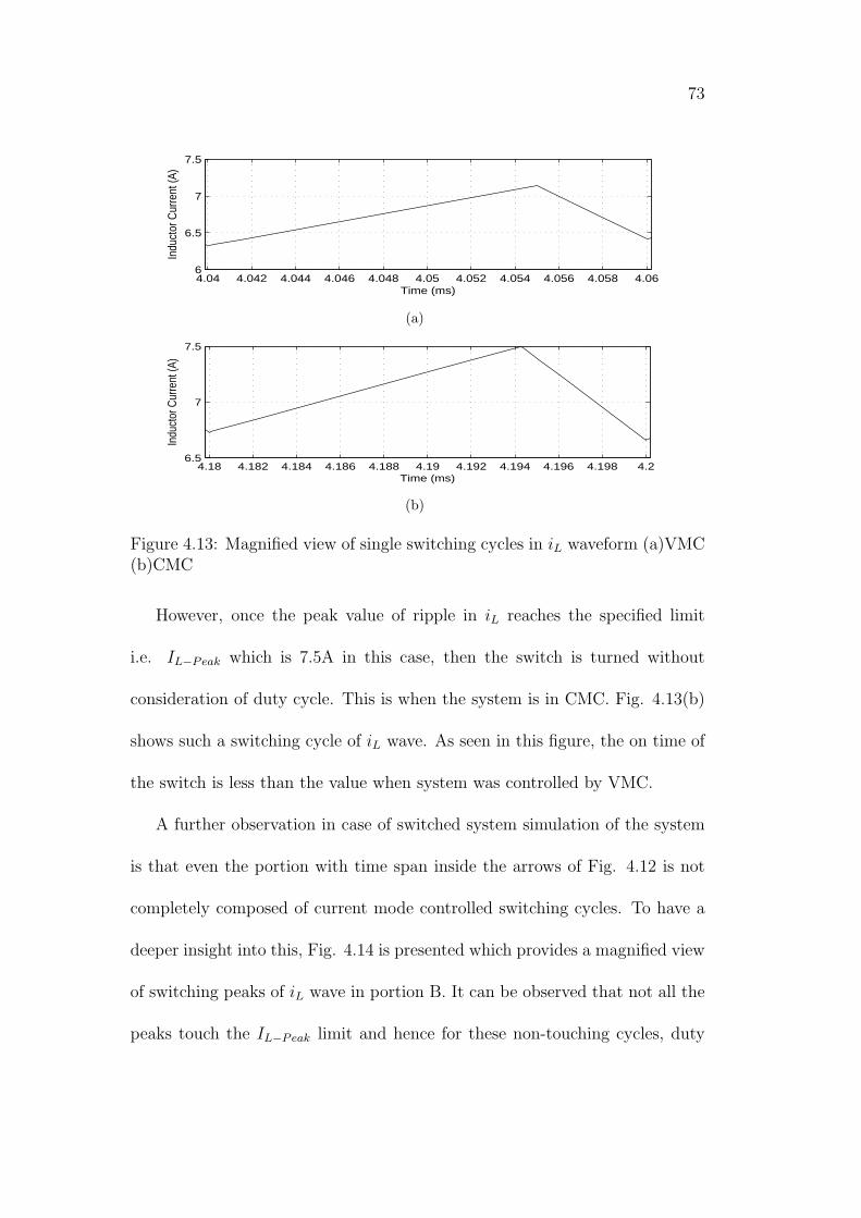
73
4.04 4.042 4.044 4.046 4.048 4.05 4.052 4.054 4.056 4.058 4.066
6.5
7
7.5
Time (ms)
Indu
ctor
Cur
rent
(A)
(a)
4.18 4.182 4.184 4.186 4.188 4.19 4.192 4.194 4.196 4.198 4.26.5
7
7.5
Time (ms)
Indu
ctor
Cur
rent
(A)
(b)
Figure 4.13: Magnified view of single switching cycles in 𝑖𝐿 waveform (a)VMC(b)CMC
However, once the peak value of ripple in 𝑖𝐿 reaches the specified limit
i.e. 𝐼𝐿−𝑃𝑒𝑎𝑘 which is 7.5A in this case, then the switch is turned without
consideration of duty cycle. This is when the system is in CMC. Fig. 4.13(b)
shows such a switching cycle of 𝑖𝐿 wave. As seen in this figure, the on time of
the switch is less than the value when system was controlled by VMC.
A further observation in case of switched system simulation of the system
is that even the portion with time span inside the arrows of Fig. 4.12 is not
completely composed of current mode controlled switching cycles. To have a
deeper insight into this, Fig. 4.14 is presented which provides a magnified view
of switching peaks of 𝑖𝐿 wave in portion B. It can be observed that not all the
peaks touch the 𝐼𝐿−𝑃𝑒𝑎𝑘 limit and hence for these non-touching cycles, duty
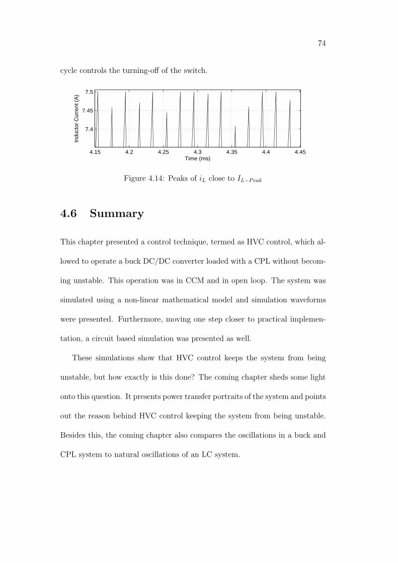
74
cycle controls the turning-off of the switch.
4.15 4.2 4.25 4.3 4.35 4.4 4.45
7.4
7.45
7.5
Time (ms)
Indu
ctor
Cur
rent
(A
)
Figure 4.14: Peaks of 𝑖𝐿 close to 𝐼𝐿−𝑃𝑒𝑎𝑘
4.6 Summary
This chapter presented a control technique, termed as HVC control, which al-
lowed to operate a buck DC/DC converter loaded with a CPL without becom-
ing unstable. This operation was in CCM and in open loop. The system was
simulated using a non-linear mathematical model and simulation waveforms
were presented. Furthermore, moving one step closer to practical implemen-
tation, a circuit based simulation was presented as well.
These simulations show that HVC control keeps the system from being
unstable, but how exactly is this done? The coming chapter sheds some light
onto this question. It presents power transfer portraits of the system and points
out the reason behind HVC control keeping the system from being unstable.
Besides this, the coming chapter also compares the oscillations in a buck and
CPL system to natural oscillations of an LC system.
Chapter 5
Power Transfer Portraits of theSystem
(Certain content in this chapter has been submitted for publication in Inter-
national Journal of Engineering, Science and Technology, 2011 [51]). In the
previous chapter, the idea of HVC control for operation of buck converter and
CPL system was presented. This chapter presents power transfer portraits of
the system under HVC control, using averaged non-linear system model. The
name power transfer portrait is given to a single figure which shows voltage,
current and power transferred in a single cycle of the system. Although certain
quantities are not to scale in this figure, however, the idea is to be able to view
and compare the shape of single cycles of the three variables.
The chapter begins with comparing the performance of buck converter and
CPL system to the behavior of an LC system. Certain deductions are made in
this regard in the first two sections, and then the discussion moves on to the
power transfer portraits of the system.
75
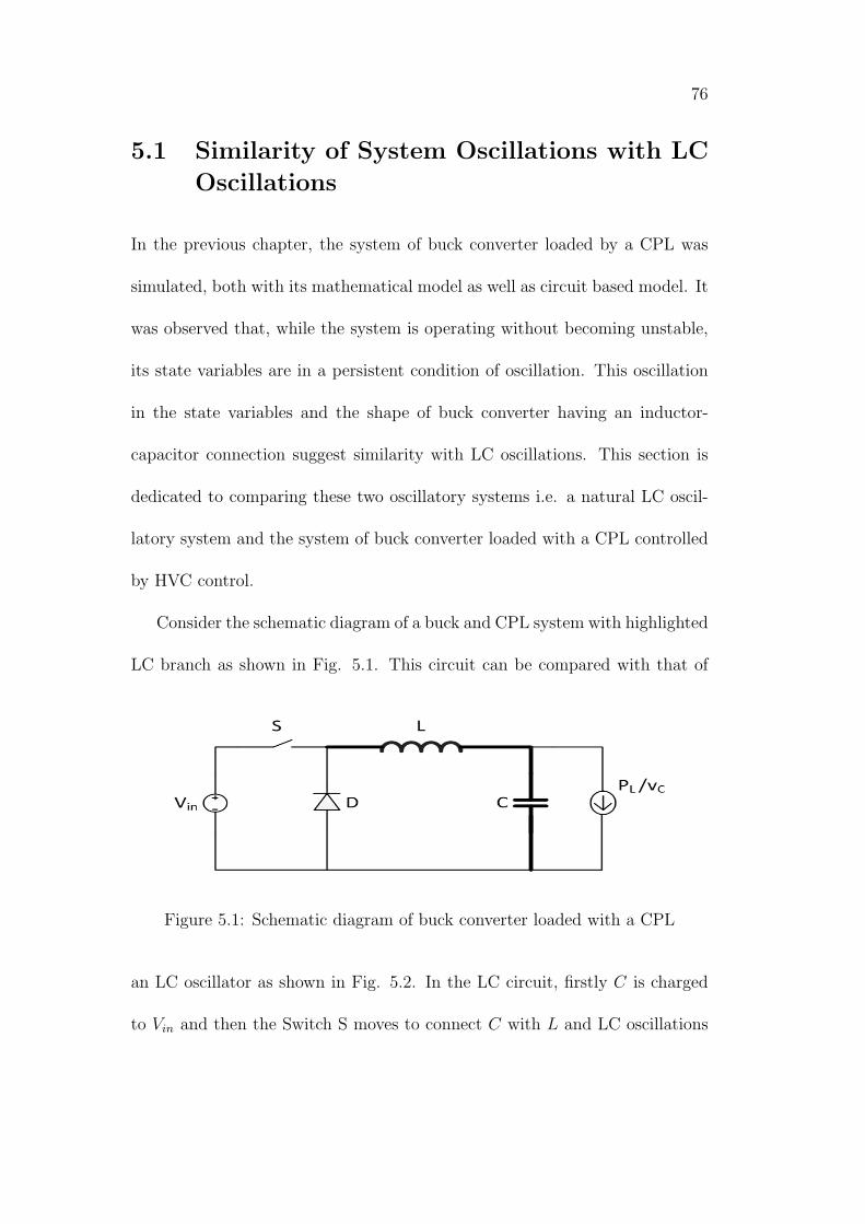
76
5.1 Similarity of System Oscillations with LC
Oscillations
In the previous chapter, the system of buck converter loaded by a CPL was
simulated, both with its mathematical model as well as circuit based model. It
was observed that, while the system is operating without becoming unstable,
its state variables are in a persistent condition of oscillation. This oscillation
in the state variables and the shape of buck converter having an inductor-
capacitor connection suggest similarity with LC oscillations. This section is
dedicated to comparing these two oscillatory systems i.e. a natural LC oscil-
latory system and the system of buck converter loaded with a CPL controlled
by HVC control.
Consider the schematic diagram of a buck and CPL system with highlighted
LC branch as shown in Fig. 5.1. This circuit can be compared with that of
Figure 5.1: Schematic diagram of buck converter loaded with a CPL
an LC oscillator as shown in Fig. 5.2. In the LC circuit, firstly 𝐶 is charged
to 𝑉𝑖𝑛 and then the Switch S moves to connect 𝐶 with 𝐿 and LC oscillations
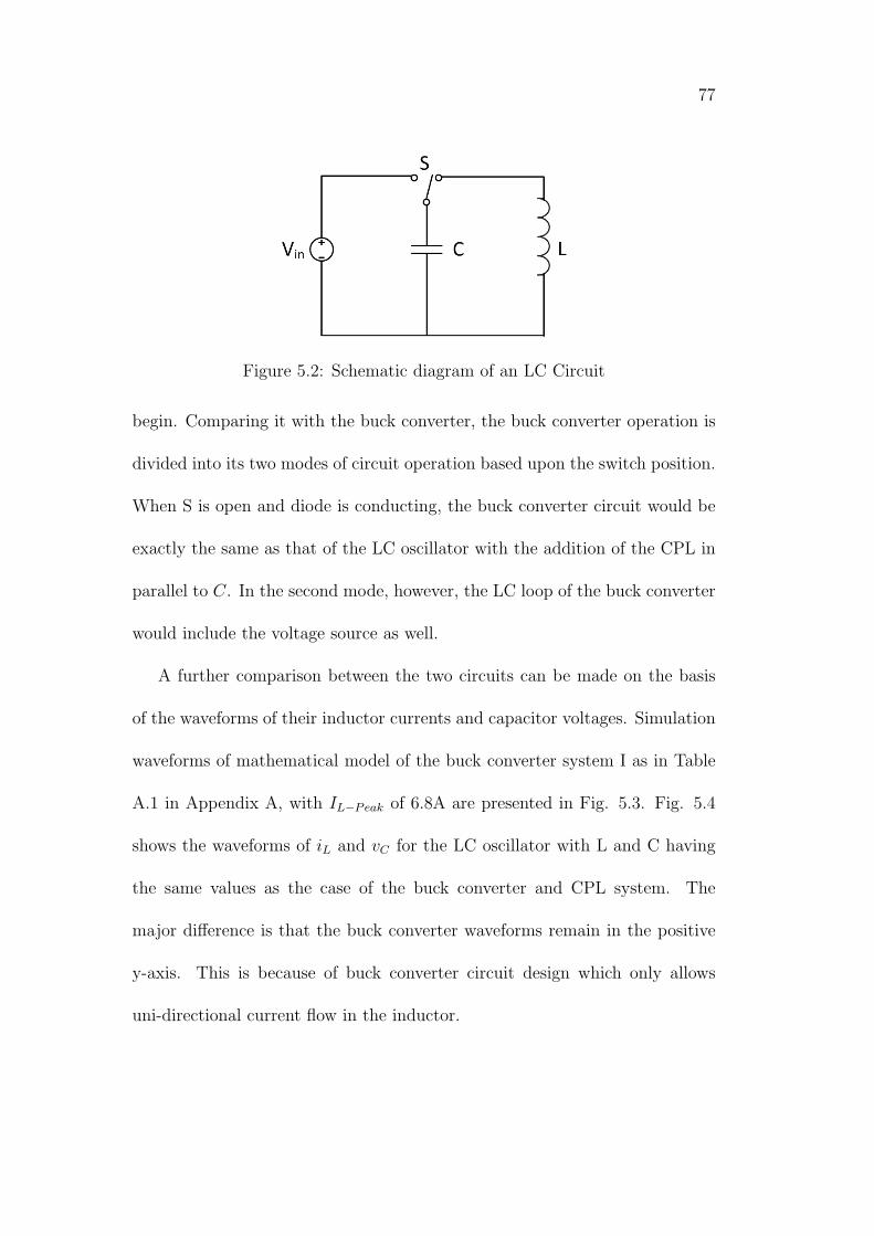
77
Figure 5.2: Schematic diagram of an LC Circuit
begin. Comparing it with the buck converter, the buck converter operation is
divided into its two modes of circuit operation based upon the switch position.
When S is open and diode is conducting, the buck converter circuit would be
exactly the same as that of the LC oscillator with the addition of the CPL in
parallel to 𝐶. In the second mode, however, the LC loop of the buck converter
would include the voltage source as well.
A further comparison between the two circuits can be made on the basis
of the waveforms of their inductor currents and capacitor voltages. Simulation
waveforms of mathematical model of the buck converter system I as in Table
A.1 in Appendix A, with 𝐼𝐿−𝑃𝑒𝑎𝑘 of 6.8A are presented in Fig. 5.3. Fig. 5.4
shows the waveforms of 𝑖𝐿 and 𝑣𝐶 for the LC oscillator with L and C having
the same values as the case of the buck converter and CPL system. The
major difference is that the buck converter waveforms remain in the positive
y-axis. This is because of buck converter circuit design which only allows
uni-directional current flow in the inductor.
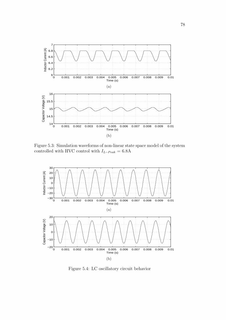
78
0 0.001 0.002 0.003 0.004 0.005 0.006 0.007 0.008 0.009 0.016
6.2
6.4
6.6
6.8
7
Time (s)
Indu
ctor
Cur
rent
(A)
(a)
0 0.001 0.002 0.003 0.004 0.005 0.006 0.007 0.008 0.009 0.0114
14.5
15
15.5
16
Time (s)
Cap
acito
r Vol
tage
(V)
(b)
Figure 5.3: Simulation waveforms of non-linear state space model of the systemcontrolled with HVC control with 𝐼𝐿−𝑃𝑒𝑎𝑘 = 6.8A
0 0.001 0.002 0.003 0.004 0.005 0.006 0.007 0.008 0.009 0.01−30
−20
−10
0
10
20
30
Time (s)
Indu
ctor
Cur
rent
(A)
(a)
0 0.001 0.002 0.003 0.004 0.005 0.006 0.007 0.008 0.009 0.01−20
−10
0
10
20
Time (s)
Cap
acito
r Vol
tage
(V)
(b)
Figure 5.4: LC oscillatory circuit behavior

79
The second difference is the flat shaped peak portions of 𝑖𝐿 wave in buck
converter waveforms and this is because of HVC control limiting 𝑖𝐿 to 𝐼𝐿−𝑃𝑒𝑎𝑘.
Actually, it is the HVC control or limiting of 𝑖𝐿 to an upper peak which is
responsible for keeping 𝑖𝐿 in the positive y-axis as well, as discussed in Section
4.2.
Because of the 𝑖𝐿 limitation, the oscillations in the buck converter system no
longer remain natural LC oscillations. Not only does the 𝑖𝐿 limitation change
the shape of the waves, but it also changes the time period of the waves. The
time period of a naturally oscillating LC system is given by the equation
𝑇 = 2𝜋√𝐿𝐶 (5.1)
and according to this equation, the time period of the LC oscillator system is
𝑇 = 2𝜋√
(0.1𝑚𝐻)(300𝜇𝐹 ) = 1.09𝑚𝑠 (5.2)
This can be observed roughly from the simulation waveforms (Fig. 5.4) of the
system as well. However, for the buck converter system, the time period for
the waves is approximately 1.3ms. Again, a proximity exists between the two
systems, but they are not exactly equal.
Hence, although there is an apparent similarity between the oscillatory
behavior of the buck with CPL system and an LC oscillator system; the two
systems are not exactly the same. Still it may be argued that the behavior of
buck and CPL system is modified or is unnatural LC oscillation.
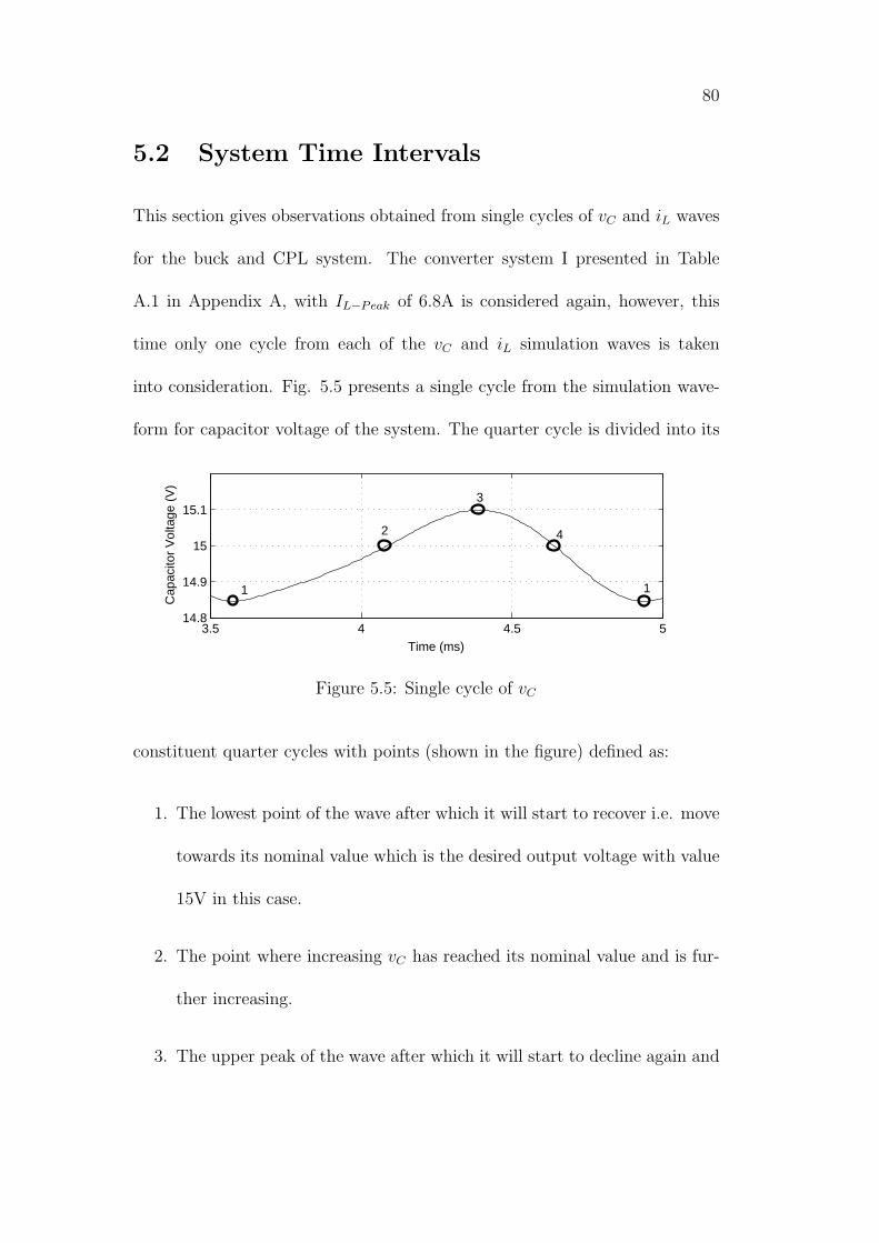
80
5.2 System Time Intervals
This section gives observations obtained from single cycles of 𝑣𝐶 and 𝑖𝐿 waves
for the buck and CPL system. The converter system I presented in Table
A.1 in Appendix A, with 𝐼𝐿−𝑃𝑒𝑎𝑘 of 6.8A is considered again, however, this
time only one cycle from each of the 𝑣𝐶 and 𝑖𝐿 simulation waves is taken
into consideration. Fig. 5.5 presents a single cycle from the simulation wave-
form for capacitor voltage of the system. The quarter cycle is divided into its
3.5 4 4.5 514.8
14.9
15
15.1
Time (ms)
Cap
acito
r V
olta
ge (
V)
1
2
3
4
1
Figure 5.5: Single cycle of 𝑣𝐶
constituent quarter cycles with points (shown in the figure) defined as:
1. The lowest point of the wave after which it will start to recover i.e. move
towards its nominal value which is the desired output voltage with value
15V in this case.
2. The point where increasing 𝑣𝐶 has reached its nominal value and is fur-
ther increasing.
3. The upper peak of the wave after which it will start to decline again and
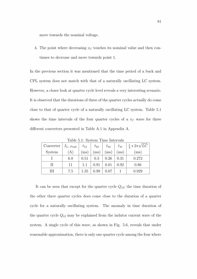
81
move towards the nominal voltage.
4. The point where decreasing 𝑣𝐶 touches its nominal value and then con-
tinues to decrease and move towards point 1.
In the previous section it was mentioned that the time period of a buck and
CPL system does not match with that of a naturally oscillating LC system.
However, a closer look at quarter cycle level reveals a very interesting scenario.
It is observed that the durations of three of the quarter cycles actually do come
close to that of quarter cycle of a naturally oscillating LC system. Table 5.1
shows the time intervals of the four quarter cycles of a 𝑣𝐶 wave for three
different converters presented in Table A.1 in Appendix A.
Table 5.1: System Time Intervals
Converter 𝐼𝐿−𝑃𝑒𝑎𝑘 𝑡12 𝑡23 𝑡34 𝑡4114∗ 2𝜋√𝐿𝐶
System (A) (ms) (ms) (ms) (ms) (ms)
I 6.8 0.51 0.3 0.26 0.31 0.272
II 11 1.1 0.91 0.81 0.92 0.86
III 7.5 1.35 0.99 0.87 1 0.929
It can be seen that except for the quarter cycle 𝑄12; the time duration of
the other three quarter cycles does come close to the duration of a quarter
cycle for a naturally oscillating system. The anomaly in time duration of
the quarter cycle 𝑄12 may be explained from the indutor current wave of the
system. A single cycle of this wave, as shown in Fig. 5.6, reveals that under
reasonable approximation, there is only one quarter cycle among the four where
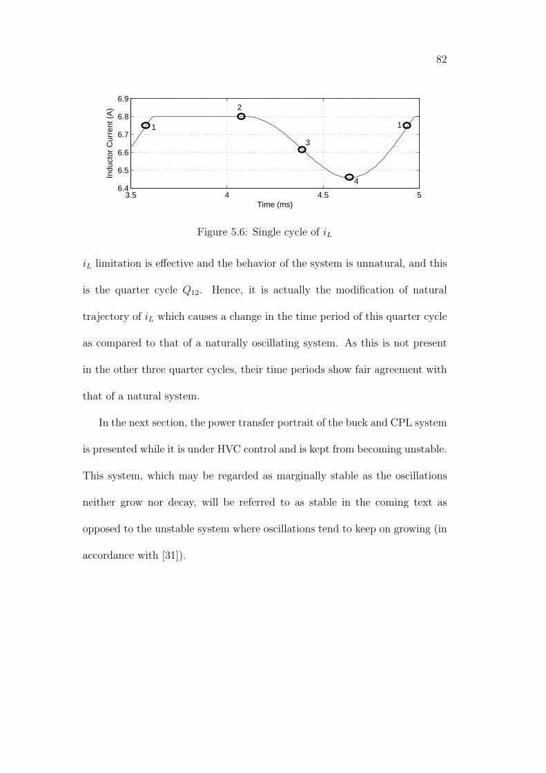
82
3.5 4 4.5 56.4
6.5
6.6
6.7
6.8
6.9
Time (ms)
Indu
ctor
Cur
rent
(A
)
3
4
11
2
Figure 5.6: Single cycle of 𝑖𝐿
𝑖𝐿 limitation is effective and the behavior of the system is unnatural, and this
is the quarter cycle 𝑄12. Hence, it is actually the modification of natural
trajectory of 𝑖𝐿 which causes a change in the time period of this quarter cycle
as compared to that of a naturally oscillating system. As this is not present
in the other three quarter cycles, their time periods show fair agreement with
that of a natural system.
In the next section, the power transfer portrait of the buck and CPL system
is presented while it is under HVC control and is kept from becoming unstable.
This system, which may be regarded as marginally stable as the oscillations
neither grow nor decay, will be referred to as stable in the coming text as
opposed to the unstable system where oscillations tend to keep on growing (in
accordance with [31]).
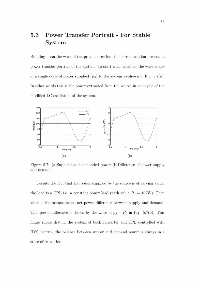
83
5.3 Power Transfer Portrait - For Stable
System
Building upon the work of the previous section, the current section presents a
power transfer portrait of the system. To start with, consider the wave shape
of a single cycle of power supplied (𝑝𝑆) to the system as shown in Fig. 5.7(a).
In other words this is the power extracted from the source in one cycle of the
modified LC oscillation of the system.
3.5 4 4.5 596
97
98
99
100
101
102
103
Time (ms)
Pow
er (W
)
pS
PL
(a)
3.5 4 4.5 5−4
−3
−2
−1
0
1
2
3
Time (ms)
pS−
PL
(W)
(b)
Figure 5.7: (a)Supplied and demanded power (b)Difference of power supplyand demand
Despite the fact that the power supplied by the source is of varying value,
the load is a CPL i.e. a constant power load (with value 𝑃𝐿 = 100W). Then
what is the instantaneous net power difference between supply and demand.
This power difference is shown by the wave of 𝑝𝑆 − 𝑃𝐿 in Fig. 5.7(b). This
figure shows that in the system of buck converter and CPL controlled with
HVC control, the balance between supply and demand power is always in a
state of transition.

84
Now observe this net power difference curve in comparison with the 𝑣𝐶 and
𝑖𝐿 waves of the system in Fig. 5.8 which is referred to as the power transfer
portrait of the system. This figure shows one cycle of 𝑝𝑆 − 𝑃𝐿 (𝑝𝑆 stands
Figure 5.8: Power Transfer Portrait
for instantaneous power supplied by the source) curve for converter system I
(Table A.1 in Appendix A) for 𝐼𝐿−𝑃𝑒𝑎𝑘 of 6.8 A. Also shown are the waves of
𝑖𝐿 − 𝐼𝐿−𝑛𝑜𝑚𝑖𝑛𝑎𝑙 and 𝑣𝐶 − 𝑉𝐶−𝑛𝑜𝑚𝑖𝑛𝑎𝑙 i.e. the curves of difference of 𝑖𝐿 and 𝑣𝐶
with respect to their nominal values. These two curves are not to scale (and
are actually enlarged in amplitude) in order to show them on the same scale
as for 𝑝𝑆 − 𝑃𝐿 curve. This allows to easily view and compare shapes of single
cycles of power transfer curve and curves of both state variables (actually their
85
differences from respective nominal values) in one figure.
As seen in this power transfer portrait, limitation of 𝑖𝐿 to a certain value in
the quarter cycle 𝑄12, hampers the rate of power extraction from the source.
As the current wave (𝑖𝐿−𝐼𝐿−𝑛𝑜𝑚𝑖𝑛𝑎𝑙) flattens after point 1; the slope of 𝑝𝑆−𝑃𝐿
wave gets a sharp decrement and an otherwise large peak is avoided for this
curve. With the reduction in slope of 𝑝𝑆 −𝑃𝐿 wave, the rate of energy storage
in the system capacitor and therefore, the rate of rise of 𝑣𝐶 will get reduced
as compared to a system with no 𝑖𝐿 limitation. This fact might be attributed
to explain the difference of time duration between this quarter cycle and the
quarter cycle of a naturally oscillating system. It can be observed in the figure
that the slope of voltage wave between points 1 and 2 appears flattened out
as compared to the other three quarter cycles of this wave which show quite
sinusoidal shape.
5.3.1 Varying Phase Difference
The power transfer portrait of the system also reveals information about the
phase difference between the state variables of 𝑣𝐶 and 𝑖𝐿. Again, their exists
some similarity the phase difference of this system, i.e. a buck and CPL system
under HVC control and the phase difference of a natural LC oscillation system.
However, the two systems do not exhibit exactly the same behavior. In the
LC system with natural oscillation, the phase difference between voltage and
current waves is 900 as shown in Fig. 5.9, on the other hand, the buck and

86
1 1.2 1.4 1.6 1.8 2 2.2−30
−20
−10
0
10
20
30
Time (ms)
Indu
ctor
Cur
rent
(A),
Cap
acito
r Vol
tage
(V)
Figure 5.9: A single cycle of LC oscillation system showing 900 phase difference
CPL system actually shows a varying phase difference. From the power transfer
portrait of the system as shown in Fig. 5.8, the following can be observed:
A. The system phase difference is 900 at points 2 and 4. This is because at
point 2, 𝑣𝐶 − 𝑉𝐶−𝑛𝑜𝑚𝑖𝑛𝑎𝑙 is at zero, which means that the actual voltage
is at its nominal value; while the inductor current wave is almost at its
positive peak. Similarly, at point 4, the voltage wave is at zero again,
while the current wave is at its negative peak.
B. At point 3, where voltage has achieved its positive peak, current has
already passed through its zero value, and hence it is leading even more
than 900 w.r.t the voltage. Similarly, at point 1, where voltage has
reached its negative peak, current has passed through zero and the phase
difference is again greater than 900.
C. It may be deduced that, points 2 and 4 are the only points where phase
difference is 900. Besides them, the phase difference is in continuous
variation.
87
5.4 An Insight Into System Stability
This section takes forward the idea of a power transfer portrait for the buck
converter and CPL system and applies this to a case of system instability. The
illuminating feature of this section is to provide an insight into the mechanism
of instability and then describe how HVC control comes into play and keeps
the system stable. Fig. 5.10 presents the power transfer portrait of the buck
converter system I (Table A.1 in Appendix A), however, for this figure, the
CPL power has been reduced to 30W. This is to keep the system in CCM for
a considerable portion of time; as for higher power values, the system shifts
to DCM quickly. Despite the reduction of CPL value, the major difference
between this system and the system of Fig. 5.8 is that here the system has no
limitation for peak inductor current i.e. the system has no 𝐼𝐿−𝑃𝑒𝑎𝑘. Simulation
waveforms for this system are given in Fig. 5.11. Also, in the power transfer
portrait, voltage and current waves are not to scale (for reasoning similar to
that given in explanation of Fig. 5.8) and quarter cycle demarcations are
shown in the second horizontal grid line with points marked on the waves.
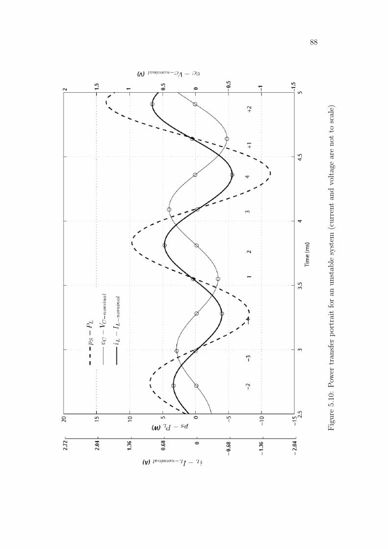
88
Figure
5.10:Pow
ertran
sfer
portraitforan
unstab
lesystem
(currentan
dvoltagearenot
toscale)
89
From the power transfer portrait of the unstable system, it can be seen
that the quarter cycle where 𝑣𝐶 wave is rising from its minimum value to
its nominal value (e.g. the quarter cycle 𝑄12 or 𝑄(+1)(+2)) is the cycle where
increasing extra power is being drawn from the source. This is characterized
by increase in 𝑝𝑆 − 𝑃𝐿 beyond the zero line close to its maximum value in
this quarter cycle. This quarter cycle may be considered as the interval which
dictates how much extra energy will be stored in the energy storage elements
of the system. As this energy keeps on increasing, and the system voltage and
current keep on increasing, system moves deeper into instability.
Consider a reverse cyclic progression of the waves starting from the peak
of (𝑖𝐿− 𝐼𝐿−𝑛𝑜𝑚𝑖𝑛𝑎𝑙) wave at point +2 in Fig. 5.10. This peak is larger than the
previous peaks and these peaks will keep on growing larger and larger in the
coming cycles if the system continues to remain in CCM. Following is a reverse
tracking investigation, with reference to Fig. 5.10, for the possible reasons of
this behavior.
A. Quarter Cycles 𝑄(+1)(+2) and 𝑄12
Consider the point +2 on the inductor current wave. For simplicity, it
is referred to as 𝑖𝐿+2, although it is actually ((𝑖𝐿 − 𝐼𝐿−𝑛𝑜𝑚𝑖𝑛𝑎𝑙)+2). This
point is the peak of inductor current wave in the quarter cycle 𝑄(+1)(+2)
and exactly one cycle prior to this, the peak point is 𝑖𝐿2. From the figure
it is observed that 𝑖𝐿+2 is larger in peak value than 𝑖𝐿2. So why is one
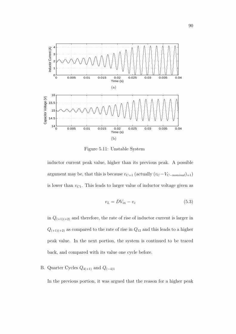
90
0 0.005 0.01 0.015 0.02 0.025 0.03 0.035 0.040
1
2
3
4
Time (s)
Indu
ctor
Cur
rent
(A)
(a)
0 0.005 0.01 0.015 0.02 0.025 0.03 0.035 0.0414
14.5
15
15.5
16
Time (s)
Cap
acito
r Vol
tage
(V)
(b)
Figure 5.11: Unstable System
inductor current peak value, higher than its previous peak. A possible
argument may be, that this is because 𝑣𝐶+1 (actually (𝑣𝐶−𝑉𝐶−𝑛𝑜𝑚𝑖𝑛𝑎𝑙)+1)
is lower than 𝑣𝐶1. This leads to larger value of inductor voltage given as
𝑣𝐿 = 𝐷𝑉𝑖𝑛 − 𝑣𝑐 (5.3)
in 𝑄(+1)(+2) and therefore, the rate of rise of inductor current is larger in
𝑄(+1)(+2) as compared to the rate of rise in 𝑄12 and this leads to a higher
peak value. In the next portion, the system is continued to be traced
back, and compared with its value one cycle before.
B. Quarter Cycles 𝑄4(+1) and 𝑄(−4)1
In the previous portion, it was argued that the reason for a higher peak
91
of inductor current was that 𝑣𝐶+1 < 𝑣𝐶1. Looking for a reason of this,
an argument can be made that this is because 𝑖𝐿4 < 𝑖𝐿−4. So, to bring
𝑖𝐿 back to its nominal value (from the value at 𝑖𝐿4) , while maintaining
constant output power, the capacitor loses more of its charge in 𝑄4(+1).
Hence 𝑣𝐶 drops more in this quarter cycle as compared to 𝑄(−4)1.
C. Quarter Cycles 𝑄34 and 𝑄(−3)(−4)
𝑖𝐿4 < 𝑖𝐿−4 because 𝑣𝐶3 > 𝑣𝐶−3, and so inductor voltage as given in
equation (5.3), is larger in magnitude (although reversed in polarity) in
𝑄34 than in 𝑄(−3)(−4). Therefore, similar to the case A, the increased rate
of change leads to a larger peak dip of inductor current wave in 𝑄(4)(+1).
D. Quarter Cycles 𝑄23 and 𝑄(−2)(−3)
𝑣𝐶3 > 𝑣𝐶−3 because 𝑖𝐿2 > 𝑖𝐿−2, so by the end of the quarter cycle 𝑄23,
all the extra energy in 𝐿 is gone to load and 𝐶. Since, load is constant
for both cycles, so, 𝑣𝐶3 is larger than 𝑣𝐶−3.
Hence, a cycle of reverse tracking completes and a positive peak of inductor
current wave is reached again (reverse tracking started from 𝑖𝐿2 and is ending
at 𝑖𝐿−2) . So the crux of the matter is that if, somehow, in the quarter cycle
involving rise of 𝑖𝐿 to its peak i.e. quarter cycles like 𝑄12 or 𝑄(+1)(+2) , 𝑖𝐿 is
not allowed from exceeding a certain value, none of the above will take place,
and along side the inductor current wave, the capacitor voltage wave will also
remain stable. This is what HVC control is actually doing. By limiting 𝑖𝐿 in
92
this quarter cycle, the addition of extra energy to the system is being limited,
which would otherwise take place in every cycle and make the system unstable.
5.5 Summary
This chapter compared the oscillations in a system of buck converter and CPL
to natural oscillations taking place in an LC system. It was observed from
quarter cycle time periods of the buck and CPL system oscillation that three
of the four quarter cycle durations were almost equal to that of corresponding
time in a natural LC oscillation system.
Subsequently, system power transfer portraits were given. Firstly, the
power transfer portrait of the system under HVC control was presented and
discussed. Then, the portrait of an unstable system was presented and an
insight into system stability was obtained from a reverse cyclic progression in
this figure.
The coming chapter presents mathematical expressions for upper voltage
peak and minimum required system capacitance in relation to the system con-
trol by HVC technique.
Chapter 6
Mathematical ExpressionsRelated to HVC Control
(Certain content in this chapter has been submitted for publication in Interna-
tional Journal of Engineering, Science and Technology, 2011 [51]). This thesis,
till now has introduced HVC control along with its simulations and an expla-
nation of system working has been presented using Power Transfer Portrait of
the system. However, mathematical expressions for different parameters have
not been included, and this is the aim of the current Chapter.
This Chapter presents expressions for upper voltage wave peak of the sys-
tem and gives a discussion about the lower peak. It has further been observed
that the system of buck converter and CPL under HVC control requires a cer-
tain minimum value for capacitor (C) to function. This too has been discussed
in this Chapter and an expression for the minimum required capacitance is
presented.
93
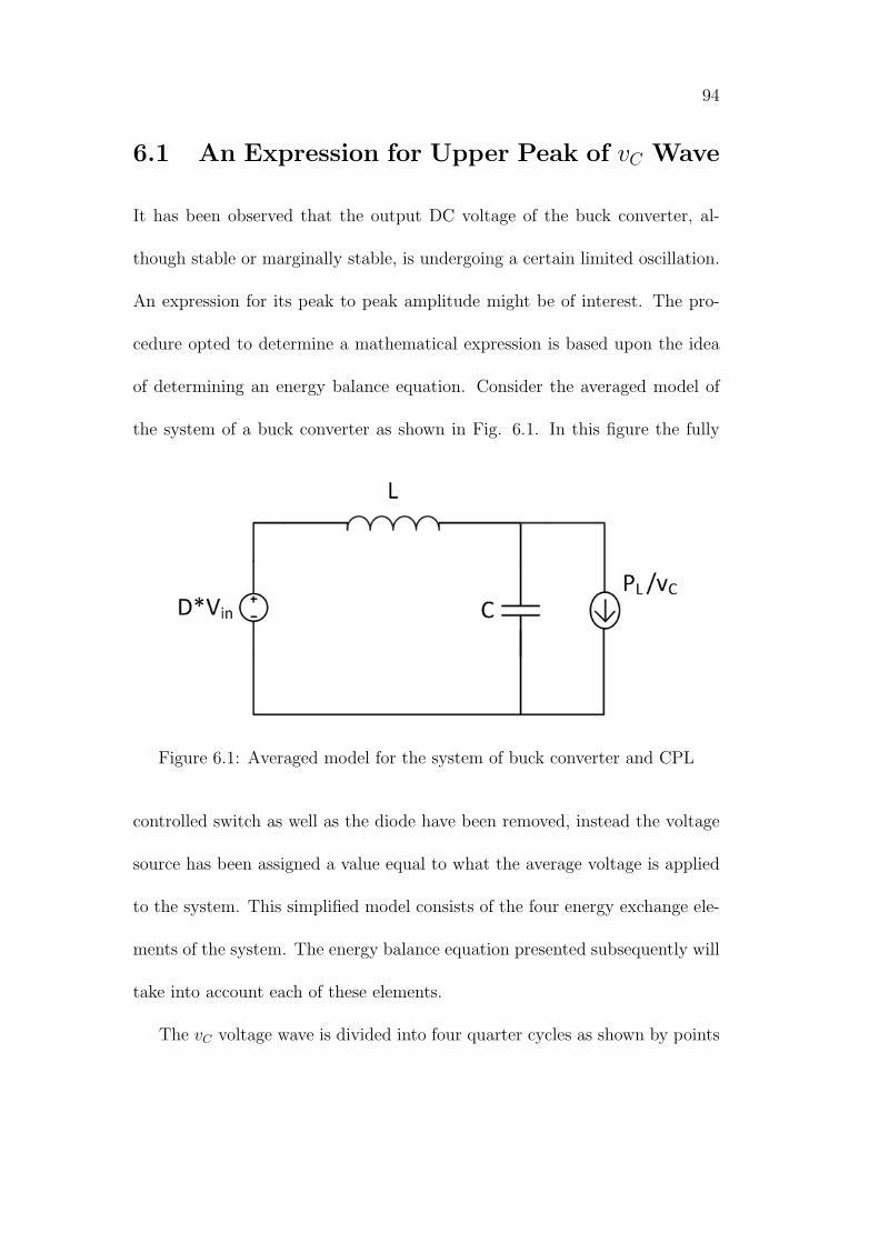
94
6.1 An Expression for Upper Peak of 𝑣𝐶 Wave
It has been observed that the output DC voltage of the buck converter, al-
though stable or marginally stable, is undergoing a certain limited oscillation.
An expression for its peak to peak amplitude might be of interest. The pro-
cedure opted to determine a mathematical expression is based upon the idea
of determining an energy balance equation. Consider the averaged model of
the system of a buck converter as shown in Fig. 6.1. In this figure the fully
Figure 6.1: Averaged model for the system of buck converter and CPL
controlled switch as well as the diode have been removed, instead the voltage
source has been assigned a value equal to what the average voltage is applied
to the system. This simplified model consists of the four energy exchange ele-
ments of the system. The energy balance equation presented subsequently will
take into account each of these elements.
The 𝑣𝐶 voltage wave is divided into four quarter cycles as shown by points
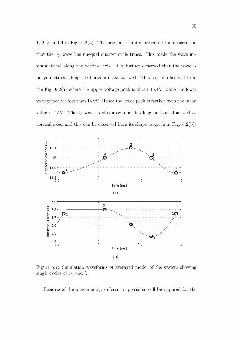
95
1, 2, 3 and 4 in Fig. 6.2(a). The previous chapter presented the observation
that the 𝑣𝐶 wave has unequal quarter cycle times. This made the wave un-
symmetrical along the vertical axis. It is further observed that the wave is
unsymmetrical along the horizontal axis as well. This can be observed from
the Fig. 6.2(a) where the upper voltage peak is about 15.1V, while the lower
voltage peak is less than 14.9V. Hence the lower peak is farther from the mean
value of 15V. (The 𝑖𝐿 wave is also unsymmetric along horizontal as well as
vertical axes, and this can be observed from its shape as given in Fig. 6.2(b))
3.5 4 4.5 514.8
14.9
15
15.1
Time (ms)
Cap
acito
r V
olta
ge (
V)
1
2
3
4
1
(a)
3.5 4 4.5 56.4
6.5
6.6
6.7
6.8
6.9
Time (ms)
Indu
ctor
Cur
rent
(A
)
3
4
11
2
(b)
Figure 6.2: Simulation waveforms of averaged model of the system showingsingle cycles of 𝑣𝐶 and 𝑖𝐿
Because of the unsymmetry, different expressions will be required for the
96
lower and upper peaks of the 𝑣𝐶 wave. Firstly, the attempt to find an ex-
pression for the upper voltage peak of this wave is presented. This upper i.e.
positive peak is shown by the point 3 of the wave in Fig. 6.2(a).
6.1.1 Choice of Quarter Cycles
Theoretically, any one of the positive quarter cycles (i.e. 𝑄23 or 𝑄34) should
be usable to write the energy balance equation involving this peak voltage.
However, the quarter cycle 𝑄23 consists of more known quantities than the
latter. This is because at point 2, both 𝑖𝐿 and 𝑣𝐶 are known, and at point 3,
where 𝑣𝐶 needs to be calculated, 𝑖𝐿 can be assumed to be at its nominal value.
𝑣𝐶−2 = 𝑉𝐶−𝑛 = 15𝑉 (6.1)
𝑖𝐿−2 = 𝐼𝐿−𝑃𝑒𝑎𝑘 = 6.8𝐴 (6.2)
Here, 𝑉𝐶−𝑛 stands for nominal value of 𝑣𝐶 .
But for point 4, again only one quantity i.e. 𝑣𝐶 is known while 𝑖𝐿 is not.
𝑣𝐶−4 = 𝑉𝐶−𝑛 = 15𝑉 (6.3)
Hence the equation involving 𝑄34 will have one more unknown value as com-
pared to the equation for 𝑄23. So the energy balance equation for 𝑄23 is
considered.
97
6.1.2 Using the Energy Balance Equation
The energy balance equation for 𝑄23 may be written as:
△𝐸𝐶 −△𝐸𝐿 − [△(𝑝𝑆 − 𝑃𝐿) ∗ 𝑡23] = 0 (6.4)
where △𝐸𝐶 and △𝐸𝐿 refer to difference in energy values of the two energy
storage components between points 2 and 3 which can be calculated based upon
values of 𝑣𝐶 and 𝑖𝐿 at the two points, 𝑝𝑆 and 𝑃𝐿 refer to instantaneous power
values of supply and load. So 𝑃𝐿 is a constant equal to the CPL value. Also,
𝑡23 is the time duration of the quarter cycle 𝑄23. In words, the energy balance
equation may be stated as, the energy gained by capacitor in this quarter
cycle is equal to the energy lost by the inductor plus the energy supplied by
the source which was in excess of the load demand.
Unlike 𝑃𝐿, 𝑝𝑆 or in other words the power extracted from the source is a
varying quantity whose value is changing throughout the quarter cycle. As a
result, the same is true for 𝑝𝑆 −𝑃𝐿. However, the initial and final values of 𝑝𝑆
are known, given as following for points 2 and 3 respectively.
𝑝𝑆−2 = 𝑉𝑆𝑜𝑢𝑟𝑐𝑒 ∗ 𝑖𝑆𝑜𝑢𝑟𝑐𝑒 = 𝑣𝐶−2 ∗ 𝑖𝐿−2 = 𝑉𝐶−𝑛 ∗ 𝐼𝐿−𝑃𝑒𝑎𝑘 (6.5)
𝑝𝑆−3 = 𝑃𝐿 (6.6)
To have a look at the distribution of 𝑝𝑆 − 𝑃𝐿 in this quarter cycle, this
varying power difference is plotted for converter system I (Table A.1 in Ap-
pendix A) with 𝐼𝐿−𝑃𝑒𝑎𝑘 of 6.8A as shown in Fig. 6.3. This figure is actually
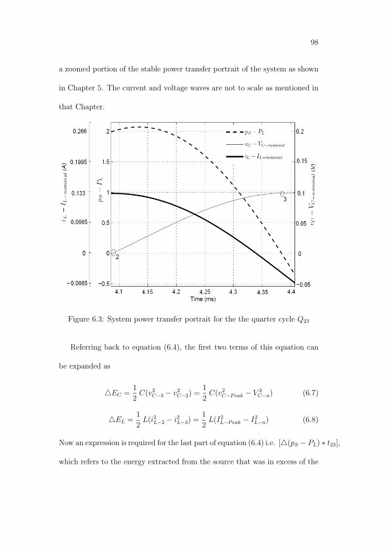
98
a zoomed portion of the stable power transfer portrait of the system as shown
in Chapter 5. The current and voltage waves are not to scale as mentioned in
that Chapter.
Figure 6.3: System power transfer portrait for the the quarter cycle 𝑄23
Referring back to equation (6.4), the first two terms of this equation can
be expanded as
△𝐸𝐶 =1
2𝐶(𝑣2𝐶−3 − 𝑣2𝐶−2) =
1
2𝐶(𝑣2𝐶−𝑃𝑒𝑎𝑘 − 𝑉 2
𝐶−𝑛) (6.7)
△𝐸𝐿 =1
2𝐿(𝑖2𝐿−2 − 𝑖2𝐿−3) =
1
2𝐿(𝐼2𝐿−𝑃𝑒𝑎𝑘 − 𝐼2𝐿−𝑛) (6.8)
Now an expression is required for the last part of equation (6.4) i.e. [△(𝑝𝑆 − 𝑃𝐿) ∗ 𝑡23],
which refers to the energy extracted from the source that was in excess of the
99
load demand, during the quarter cycle 𝑄23. This energy is equal to the area
under the dotted 𝑝𝑆 − 𝑃𝐿 curve in Fig. 6.3.
6.1.3 Triangular Approximation for area under the curve
To start with, the region unders this curve is approximated to a triangle and
the area under the curve or energy during this quarter cycle is approximated
by the formula of area of a triangle.
△(𝑝𝑆 − 𝑃𝐿) ∗ 𝑡23 = 1
2∗ 𝑏𝑎𝑠𝑒 ∗ ℎ𝑒𝑖𝑔ℎ𝑡 = 1
2∗ 𝑡23 ∗ (𝑝𝑆−2 − 𝑃𝐿) (6.9)
For the triangular assumption of 𝑝𝑆 − 𝑃𝐿 curve, it is further assumed that
the height of the triangle is the value of this curve at point 2. This can be
regarded as slightly erroneous because the curve rises little more after this point
as shown in Fig. 6.3. Now that the expressions for each of the three terms
in the original energy balance equation (6.4) are available as (6.7), (6.8) and
(6.9), using these expressions in the original equation provides an expression
for the upper voltage peak given as,
𝑣𝐶−3 =
√[1
𝐶∗ (𝑝𝑆−2 − 𝑃𝐿) ∗ 𝑡23
]+
[𝐿
𝐶∗ (𝑖2𝐿−2 − 𝑖2𝐿−3)
]+ 𝑣2𝐶−2 (6.10)
or, it can also be written as;
𝑣𝐶−𝑃𝑒𝑎𝑘 =
√[1
𝐶∗ (𝑉𝐶−𝑛𝐼𝐿−𝑃𝑒𝑎𝑘 − 𝑃𝐿)𝑡23
]+
[𝐿
𝐶∗ (𝐼2𝐿−𝑃𝑒𝑎𝑘 − 𝐼2𝐿−𝑛)
]+ 𝑉 2
𝐶−𝑛
(6.11)
In this expression 𝑡23 may be regarded as the only unknown quantity as
all other value are known or assumed. For the time being, actual value of
100
𝑡23 as measured from simulation is used and the results of using the equation
are presented. This method, although based upon rather crude assumptions,
provides satisfactory results as shown in Table 6.1.
6.1.4 Attempt to increase accuracy
A more accurate expression, however, is apparently unachievable without the
loss of generality. 𝑖𝐿−3 needs to be replaced by the actual value of inductor
current at point 3, and the actual area under the 𝑝𝑆 − 𝑃𝐿 curve is required.
To find this area, the procedure adopted here involves curve fitting. Using
MATLAB a polynomial can be determined which will approximate the 𝑝𝑆−𝑃𝐿
curve for the quarter cycle 𝑄23. For the particular case of converter system
I (Table A.1 in Appendix A) with 𝐼𝐿−𝑃𝑒𝑎𝑘 of 6.8A, this polynomial may be
written as:
(𝑝𝑆 − 𝑃𝐿)𝑡−23 = 1.993 + 3244.6𝑡− (3.42 ∗ 107)𝑡2 (6.12)
To get a final expression for peak voltage, this expression for 𝑝𝑆 −𝑃𝐿 needs to
be solved for area under the curve for the duration of the quarter cycle 𝑄23.
Using this value, now referred to as 𝑎𝑟𝑒𝑎23, the final equation for the peak 𝑣𝐶
or 𝑣𝐶−3 can be derived as:
△𝐸𝐶 −△𝐸𝐿 − [△(𝑝𝑆 − 𝑃𝐿) ∗ 𝑡23] = 0 (6.13)
𝑠𝑜 △ 𝐸𝐶 −△𝐸𝐿 − 𝑎𝑟𝑒𝑎23 = 0 (6.14)
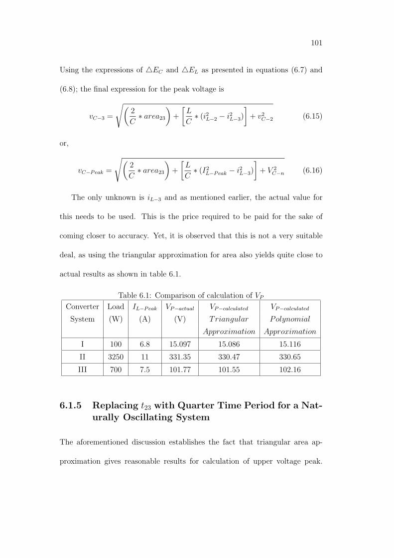
101
Using the expressions of △𝐸𝐶 and △𝐸𝐿 as presented in equations (6.7) and
(6.8); the final expression for the peak voltage is
𝑣𝐶−3 =
√(2
𝐶∗ 𝑎𝑟𝑒𝑎23
)+
[𝐿
𝐶∗ (𝑖2𝐿−2 − 𝑖2𝐿−3)
]+ 𝑣2𝐶−2 (6.15)
or,
𝑣𝐶−𝑃𝑒𝑎𝑘 =
√(2
𝐶∗ 𝑎𝑟𝑒𝑎23
)+
[𝐿
𝐶∗ (𝐼2𝐿−𝑃𝑒𝑎𝑘 − 𝑖2𝐿−3)
]+ 𝑉 2
𝐶−𝑛 (6.16)
The only unknown is 𝑖𝐿−3 and as mentioned earlier, the actual value for
this needs to be used. This is the price required to be paid for the sake of
coming closer to accuracy. Yet, it is observed that this is not a very suitable
deal, as using the triangular approximation for area also yields quite close to
actual results as shown in table 6.1.
Table 6.1: Comparison of calculation of 𝑉𝑃
Converter Load 𝐼𝐿−𝑃𝑒𝑎𝑘 𝑉𝑃−𝑎𝑐𝑡𝑢𝑎𝑙 𝑉𝑃−𝑐𝑎𝑙𝑐𝑢𝑙𝑎𝑡𝑒𝑑 𝑉𝑃−𝑐𝑎𝑙𝑐𝑢𝑙𝑎𝑡𝑒𝑑
System (W) (A) (V) 𝑇𝑟𝑖𝑎𝑛𝑔𝑢𝑙𝑎𝑟 𝑃𝑜𝑙𝑦𝑛𝑜𝑚𝑖𝑎𝑙
𝐴𝑝𝑝𝑟𝑜𝑥𝑖𝑚𝑎𝑡𝑖𝑜𝑛 𝐴𝑝𝑝𝑟𝑜𝑥𝑖𝑚𝑎𝑡𝑖𝑜𝑛
I 100 6.8 15.097 15.086 15.116
II 3250 11 331.35 330.47 330.65
III 700 7.5 101.77 101.55 102.16
6.1.5 Replacing 𝑡23 with Quarter Time Period for a Nat-urally Oscillating System
The aforementioned discussion establishes the fact that triangular area ap-
proximation gives reasonable results for calculation of upper voltage peak.
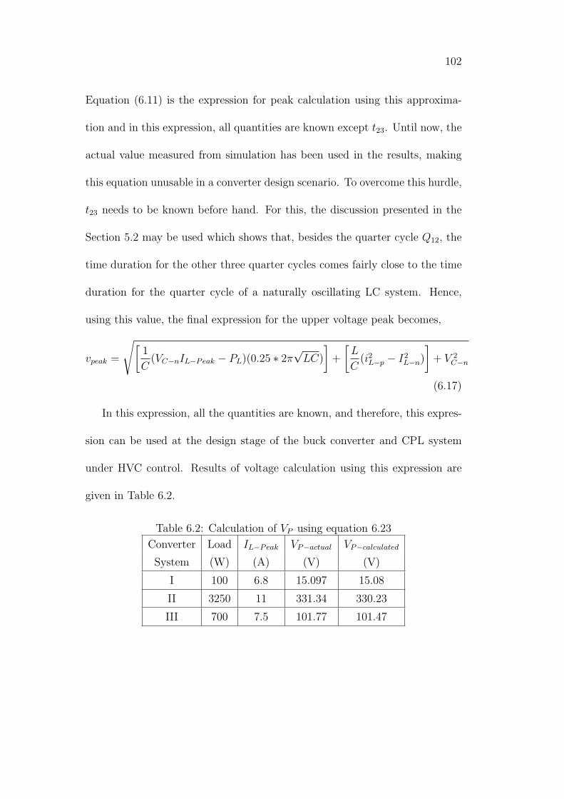
102
Equation (6.11) is the expression for peak calculation using this approxima-
tion and in this expression, all quantities are known except 𝑡23. Until now, the
actual value measured from simulation has been used in the results, making
this equation unusable in a converter design scenario. To overcome this hurdle,
𝑡23 needs to be known before hand. For this, the discussion presented in the
Section 5.2 may be used which shows that, besides the quarter cycle 𝑄12, the
time duration for the other three quarter cycles comes fairly close to the time
duration for the quarter cycle of a naturally oscillating LC system. Hence,
using this value, the final expression for the upper voltage peak becomes,
𝑣𝑝𝑒𝑎𝑘 =
√[1
𝐶(𝑉𝐶−𝑛𝐼𝐿−𝑃𝑒𝑎𝑘 − 𝑃𝐿)(0.25 ∗ 2𝜋
√𝐿𝐶)
]+
[𝐿
𝐶(𝑖2𝐿−𝑝 − 𝐼2𝐿−𝑛)
]+ 𝑉 2
𝐶−𝑛
(6.17)
In this expression, all the quantities are known, and therefore, this expres-
sion can be used at the design stage of the buck converter and CPL system
under HVC control. Results of voltage calculation using this expression are
given in Table 6.2.
Table 6.2: Calculation of 𝑉𝑃 using equation 6.23
Converter Load 𝐼𝐿−𝑃𝑒𝑎𝑘 𝑉𝑃−𝑎𝑐𝑡𝑢𝑎𝑙 𝑉𝑃−𝑐𝑎𝑙𝑐𝑢𝑙𝑎𝑡𝑒𝑑
System (W) (A) (V) (V)
I 100 6.8 15.097 15.08
II 3250 11 331.34 330.23
III 700 7.5 101.77 101.47
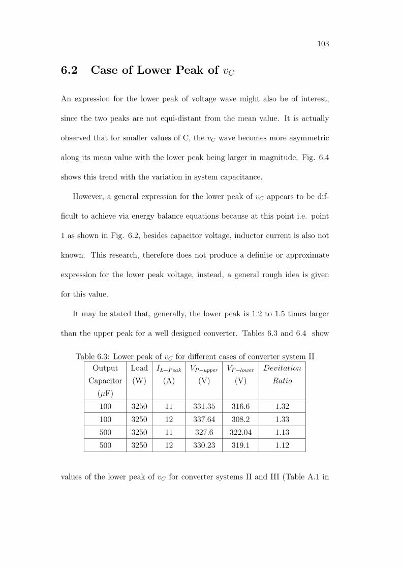
103
6.2 Case of Lower Peak of 𝑣𝐶
An expression for the lower peak of voltage wave might also be of interest,
since the two peaks are not equi-distant from the mean value. It is actually
observed that for smaller values of C, the 𝑣𝐶 wave becomes more asymmetric
along its mean value with the lower peak being larger in magnitude. Fig. 6.4
shows this trend with the variation in system capacitance.
However, a general expression for the lower peak of 𝑣𝐶 appears to be dif-
ficult to achieve via energy balance equations because at this point i.e. point
1 as shown in Fig. 6.2, besides capacitor voltage, inductor current is also not
known. This research, therefore does not produce a definite or approximate
expression for the lower peak voltage, instead, a general rough idea is given
for this value.
It may be stated that, generally, the lower peak is 1.2 to 1.5 times larger
than the upper peak for a well designed converter. Tables 6.3 and 6.4 show
Table 6.3: Lower peak of 𝑣𝐶 for different cases of converter system II
Output Load 𝐼𝐿−𝑃𝑒𝑎𝑘 𝑉𝑃−𝑢𝑝𝑝𝑒𝑟 𝑉𝑃−𝑙𝑜𝑤𝑒𝑟 𝐷𝑒𝑣𝑖𝑡𝑎𝑡𝑖𝑜𝑛
Capacitor (W) (A) (V) (V) 𝑅𝑎𝑡𝑖𝑜
(𝜇F)
100 3250 11 331.35 316.6 1.32
100 3250 12 337.64 308.2 1.33
500 3250 11 327.6 322.04 1.13
500 3250 12 330.23 319.1 1.12
values of the lower peak of 𝑣𝐶 for converter systems II and III (Table A.1 in
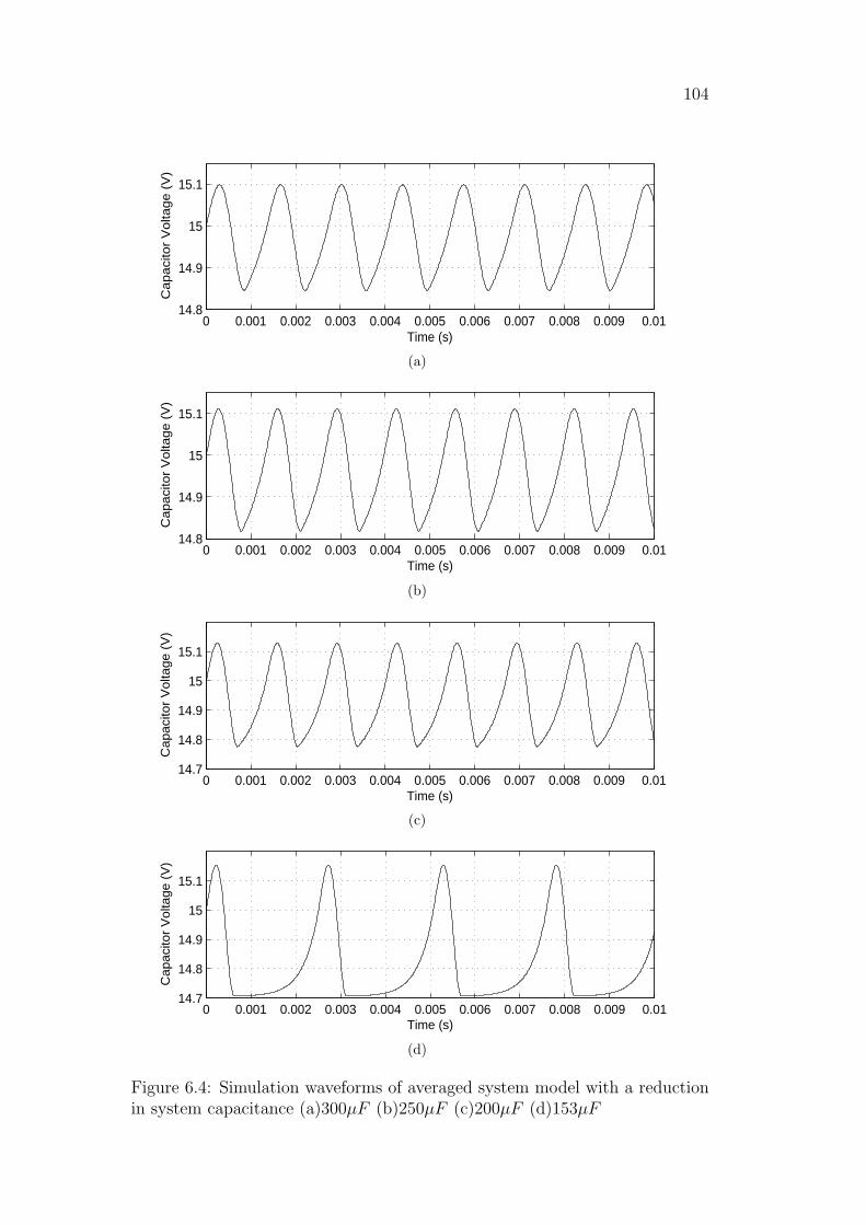
104
0 0.001 0.002 0.003 0.004 0.005 0.006 0.007 0.008 0.009 0.0114.8
14.9
15
15.1
Time (s)
Capaci
tor
Volta
ge (
V)
(a)
0 0.001 0.002 0.003 0.004 0.005 0.006 0.007 0.008 0.009 0.0114.8
14.9
15
15.1
Time (s)
Capaci
tor
Volta
ge (
V)
(b)
0 0.001 0.002 0.003 0.004 0.005 0.006 0.007 0.008 0.009 0.0114.7
14.8
14.9
15
15.1
Time (s)
Cap
acito
r V
olta
ge (
V)
(c)
0 0.001 0.002 0.003 0.004 0.005 0.006 0.007 0.008 0.009 0.0114.7
14.8
14.9
15
15.1
Time (s)
Cap
acito
r V
olta
ge (
V)
(d)
Figure 6.4: Simulation waveforms of averaged system model with a reductionin system capacitance (a)300𝜇𝐹 (b)250𝜇𝐹 (c)200𝜇𝐹 (d)153𝜇𝐹
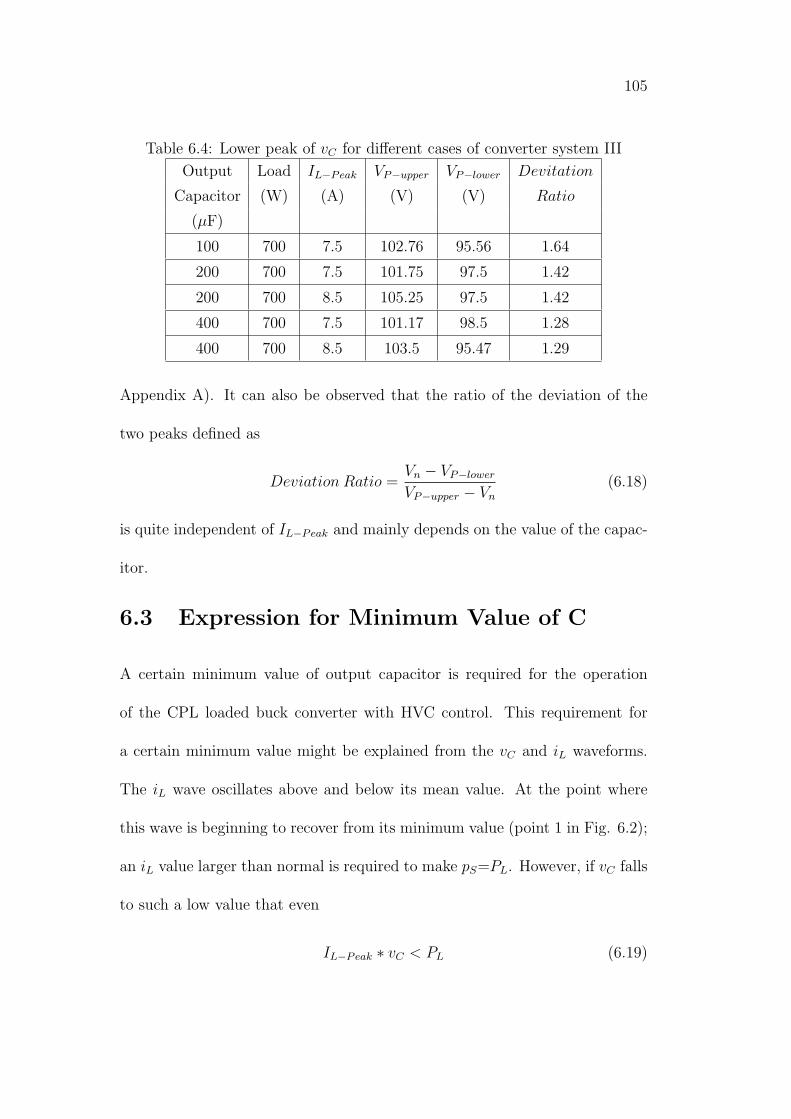
105
Table 6.4: Lower peak of 𝑣𝐶 for different cases of converter system III
Output Load 𝐼𝐿−𝑃𝑒𝑎𝑘 𝑉𝑃−𝑢𝑝𝑝𝑒𝑟 𝑉𝑃−𝑙𝑜𝑤𝑒𝑟 𝐷𝑒𝑣𝑖𝑡𝑎𝑡𝑖𝑜𝑛
Capacitor (W) (A) (V) (V) 𝑅𝑎𝑡𝑖𝑜
(𝜇F)
100 700 7.5 102.76 95.56 1.64
200 700 7.5 101.75 97.5 1.42
200 700 8.5 105.25 97.5 1.42
400 700 7.5 101.17 98.5 1.28
400 700 8.5 103.5 95.47 1.29
Appendix A). It can also be observed that the ratio of the deviation of the
two peaks defined as
𝐷𝑒𝑣𝑖𝑎𝑡𝑖𝑜𝑛 𝑅𝑎𝑡𝑖𝑜 =𝑉𝑛 − 𝑉𝑃−𝑙𝑜𝑤𝑒𝑟
𝑉𝑃−𝑢𝑝𝑝𝑒𝑟 − 𝑉𝑛
(6.18)
is quite independent of 𝐼𝐿−𝑃𝑒𝑎𝑘 and mainly depends on the value of the capac-
itor.
6.3 Expression for Minimum Value of C
A certain minimum value of output capacitor is required for the operation
of the CPL loaded buck converter with HVC control. This requirement for
a certain minimum value might be explained from the 𝑣𝐶 and 𝑖𝐿 waveforms.
The 𝑖𝐿 wave oscillates above and below its mean value. At the point where
this wave is beginning to recover from its minimum value (point 1 in Fig. 6.2);
an 𝑖𝐿 value larger than normal is required to make 𝑝𝑆=𝑃𝐿. However, if 𝑣𝐶 falls
to such a low value that even
𝐼𝐿−𝑃𝑒𝑎𝑘 ∗ 𝑣𝐶 < 𝑃𝐿 (6.19)
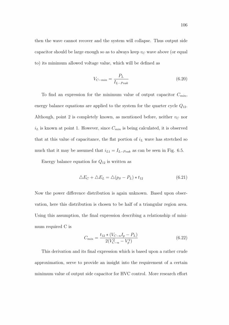
106
then the wave cannot recover and the system will collapse. Thus output side
capacitor should be large enough so as to always keep 𝑣𝐶 wave above (or equal
to) its minimum allowed voltage value, which will be defined as
𝑉𝐶−𝑚𝑖𝑛 =𝑃𝐿
𝐼𝐿−𝑃𝑒𝑎𝑘
(6.20)
To find an expression for the minimum value of output capacitor 𝐶𝑚𝑖𝑛,
energy balance equations are applied to the system for the quarter cycle 𝑄12.
Although, point 2 is completely known, as mentioned before, neither 𝑣𝐶 nor
𝑖𝐿 is known at point 1. However, since 𝐶𝑚𝑖𝑛 is being calculated, it is observed
that at this value of capacitance, the flat portion of 𝑖𝐿 wave has stretched so
much that it may be assumed that 𝑖𝐿1 = 𝐼𝐿−𝑃𝑒𝑎𝑘 as can be seen in Fig. 6.5.
Energy balance equation for 𝑄12 is written as
△𝐸𝐶 +△𝐸𝐿 = △(𝑝𝑆 − 𝑃𝐿) ∗ 𝑡12 (6.21)
Now the power difference distribution is again unknown. Based upon obser-
vation, here this distribution is chosen to be half of a triangular region area.
Using this assumption, the final expression describing a relationship of mini-
mum required C is
𝐶𝑚𝑖𝑛 =𝑡12 ∗ (𝑉𝐶−𝑛𝐼𝑝 − 𝑃𝐿)
2(𝑉 2𝐶−𝑛 − 𝑉 2
𝑝 )(6.22)
This derivation and its final expression which is based upon a rather crude
approximation, serve to provide an insight into the requirement of a certain
minimum value of output side capacitor for HVC control. More research effort
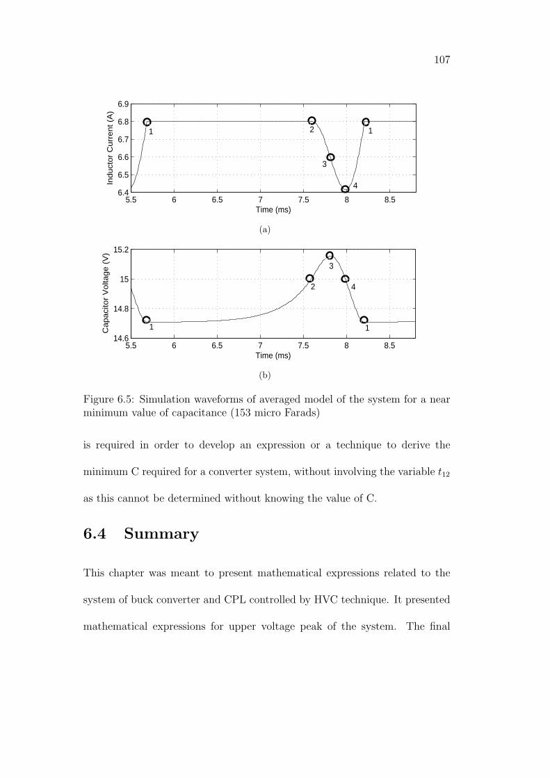
107
5.5 6 6.5 7 7.5 8 8.56.4
6.5
6.6
6.7
6.8
6.9
Time (ms)
Induct
or
Curr
ent (A
)
1 2
3
4
1
(a)
5.5 6 6.5 7 7.5 8 8.514.6
14.8
15
15.2
Time (ms)
Capaci
tor
Volta
ge (
V)
1
2
1
4
3
(b)
Figure 6.5: Simulation waveforms of averaged model of the system for a nearminimum value of capacitance (153 micro Farads)
is required in order to develop an expression or a technique to derive the
minimum C required for a converter system, without involving the variable 𝑡12
as this cannot be determined without knowing the value of C.
6.4 Summary
This chapter was meant to present mathematical expressions related to the
system of buck converter and CPL controlled by HVC technique. It presented
mathematical expressions for upper voltage peak of the system. The final
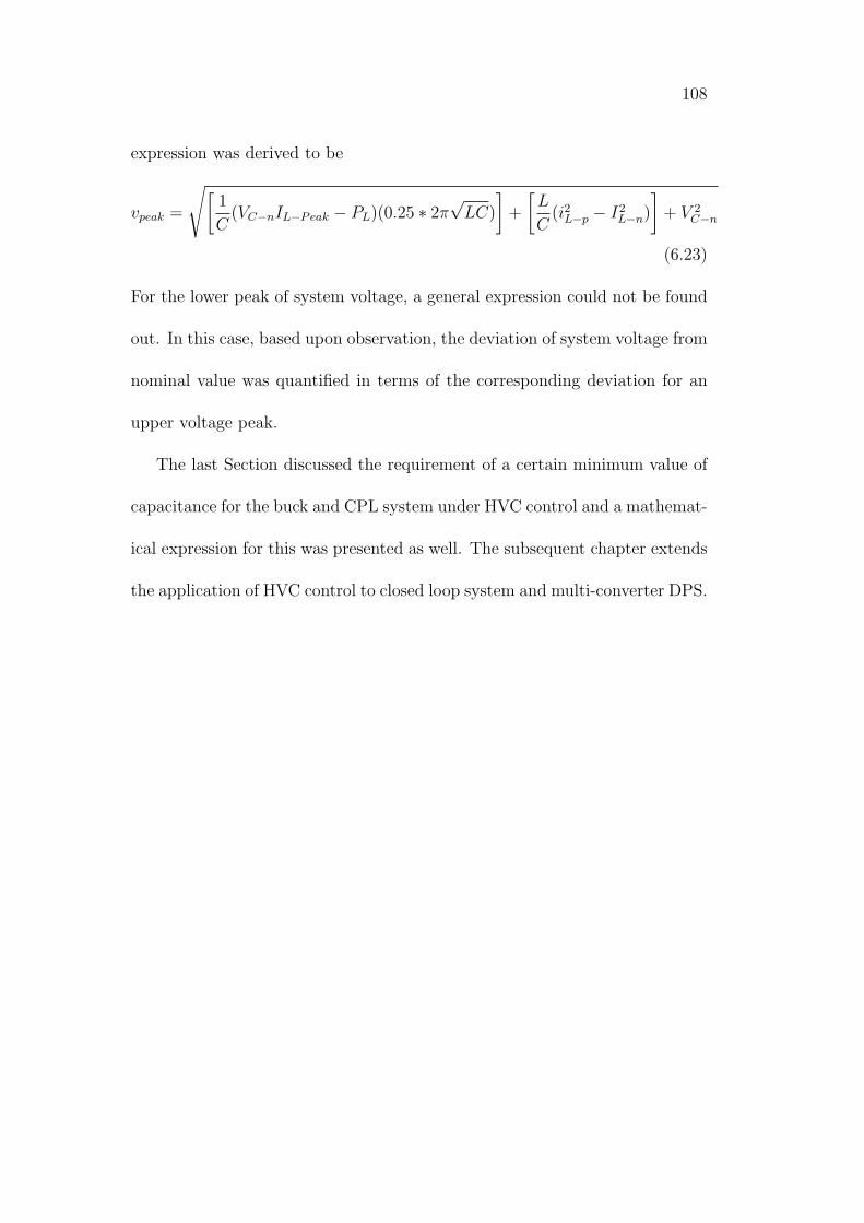
108
expression was derived to be
𝑣𝑝𝑒𝑎𝑘 =
√[1
𝐶(𝑉𝐶−𝑛𝐼𝐿−𝑃𝑒𝑎𝑘 − 𝑃𝐿)(0.25 ∗ 2𝜋
√𝐿𝐶)
]+
[𝐿
𝐶(𝑖2𝐿−𝑝 − 𝐼2𝐿−𝑛)
]+ 𝑉 2
𝐶−𝑛
(6.23)
For the lower peak of system voltage, a general expression could not be found
out. In this case, based upon observation, the deviation of system voltage from
nominal value was quantified in terms of the corresponding deviation for an
upper voltage peak.
The last Section discussed the requirement of a certain minimum value of
capacitance for the buck and CPL system under HVC control and a mathemat-
ical expression for this was presented as well. The subsequent chapter extends
the application of HVC control to closed loop system and multi-converter DPS.
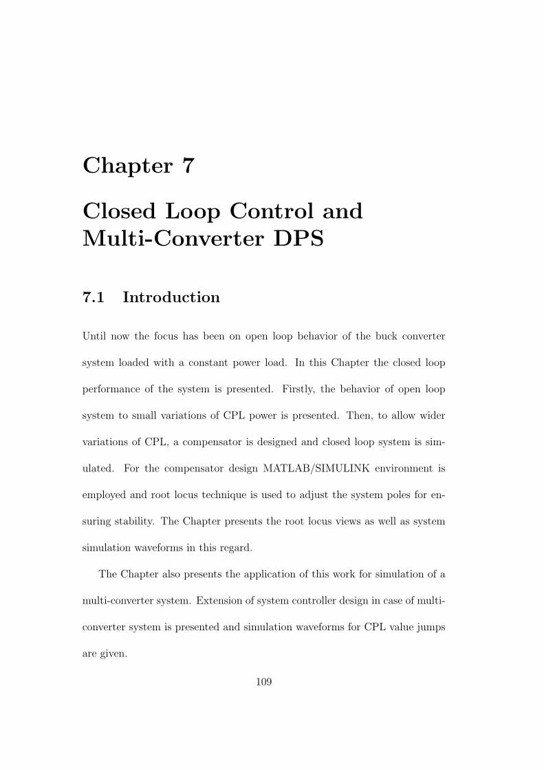
Chapter 7
Closed Loop Control andMulti-Converter DPS
7.1 Introduction
Until now the focus has been on open loop behavior of the buck converter
system loaded with a constant power load. In this Chapter the closed loop
performance of the system is presented. Firstly, the behavior of open loop
system to small variations of CPL power is presented. Then, to allow wider
variations of CPL, a compensator is designed and closed loop system is sim-
ulated. For the compensator design MATLAB/SIMULINK environment is
employed and root locus technique is used to adjust the system poles for en-
suring stability. The Chapter presents the root locus views as well as system
simulation waveforms in this regard.
The Chapter also presents the application of this work for simulation of a
multi-converter system. Extension of system controller design in case of multi-
converter system is presented and simulation waveforms for CPL value jumps
are given.
109
110
7.2 Performance of Open Loop System with
Small Variations in CPL Value
The buck converter loaded by a constant power load and controlled by HVC
technique in open loop is tested against small disturbances of CPL value.
The output CPL power value is varied and the performance of the system is
checked. It is observed that for a specified value of peak current limit for the
system, reduction in output CPL power increases the oscillation amplitude of
the inductor current. This is because the mean value of current required is
reduced and therefore, the difference of the new mean value and peak current
limit has increased. This leads to larger oscillations of inductor current and
output voltage. Conversely, the increase of output CPL power causes the
oscillation amplitude to decrease.
This actually means that the system could have been operated with a
lower limit of peak current previously, before the output CPL was increased.
However, this margin may be necessary to be maintained, keeping in view a
possible increase of CPL power. This is because operating with a nominal
current too close to the peak current limit will reduce the range of further
increase in power due to a system disturbance. This should however, not be
confused with the closed loop performance of the system, to be discussed later
(Section 7.3), where a controller varies the peak current limit thus allowing
large variations in output power of the system.
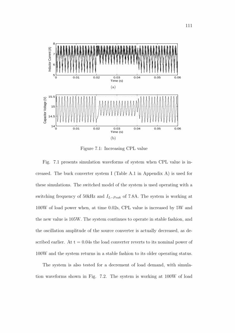
111
0 0.01 0.02 0.03 0.04 0.05 0.065
6
7
8
Time (s)
Indu
ctor
Cur
rent
(A)
(a)
0 0.01 0.02 0.03 0.04 0.05 0.0614
14.5
15
15.5
Time (s)
Cap
acito
r Vol
tage
(V)
(b)
Figure 7.1: Increasing CPL value
Fig. 7.1 presents simulation waveforms of system when CPL value is in-
creased. The buck converter system I (Table A.1 in Appendix A) is used for
these simulations. The switched model of the system is used operating with a
switching frequency of 50kHz and 𝐼𝐿−𝑃𝑒𝑎𝑘 of 7.8A. The system is working at
100W of load power when, at time 0.02s, CPL value is increased by 5W and
the new value is 105W. The system continues to operate in stable fashion, and
the oscillation amplitude of the source converter is actually decreased, as de-
scribed earlier. At t = 0.04s the load converter reverts to its nominal power of
100W and the system returns in a stable fashion to its older operating status.
The system is also tested for a decrement of load demand, with simula-
tion waveforms shown in Fig. 7.2. The system is working at 100W of load
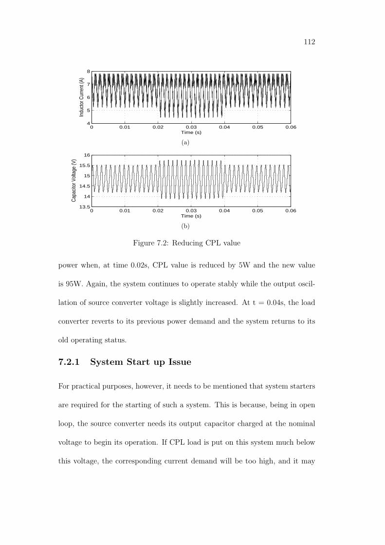
112
0 0.01 0.02 0.03 0.04 0.05 0.064
5
6
7
8
Time (s)
Indu
ctor
Cur
rent
(A)
(a)
0 0.01 0.02 0.03 0.04 0.05 0.0613.5
14
14.5
15
15.5
16
Time (s)
Cap
acito
r Vol
tage
(V)
(b)
Figure 7.2: Reducing CPL value
power when, at time 0.02s, CPL value is reduced by 5W and the new value
is 95W. Again, the system continues to operate stably while the output oscil-
lation of source converter voltage is slightly increased. At t = 0.04s, the load
converter reverts to its previous power demand and the system returns to its
old operating status.
7.2.1 System Start up Issue
For practical purposes, however, it needs to be mentioned that system starters
are required for the starting of such a system. This is because, being in open
loop, the source converter needs its output capacitor charged at the nominal
voltage to begin its operation. If CPL load is put on this system much below
this voltage, the corresponding current demand will be too high, and it may
113
be more than the peak current limit of the system. Such, a system will not
attain stable state of operation.
However, this task may be achieved by a switch, which connects the loads
to the source converter, only when its capacitor has reached its desired nominal
operating voltage. Alternatively, the loads can be given proper start-up mech-
anism allowing them to behave as constant power drawing loads only when
the capacitor has charged to a certain suitable voltage.
7.3 Closed Loop System Operation
The open loop system is not suitable for allowing large variations in output
CPL value, as can be deduced from the earlier portion of this Chapter. To
allow for this functionality, a closed loop system is required where a system
controller will be performing the task of adjusting the 𝐼𝐿−𝑃𝑒𝑎𝑘 of the system
based upon actual system load.
A PI (Proportional-Integral) type controller is used here for the closed loop
system. A schematic view of the closed loop system is shown in Fig. 7.3. For
designing the controller parameters, the averaged mathematical model of the
system is used in SIMULINK. This design can be performed via Root Locus
technique. The CPL power value in the mathematical model is set to its
maximum expected value in the system. Compensator design is performed
in MATLAB for CPL value as system input and capacitor voltage as system
output. MATLAB plots the step response of the system for a given value of the
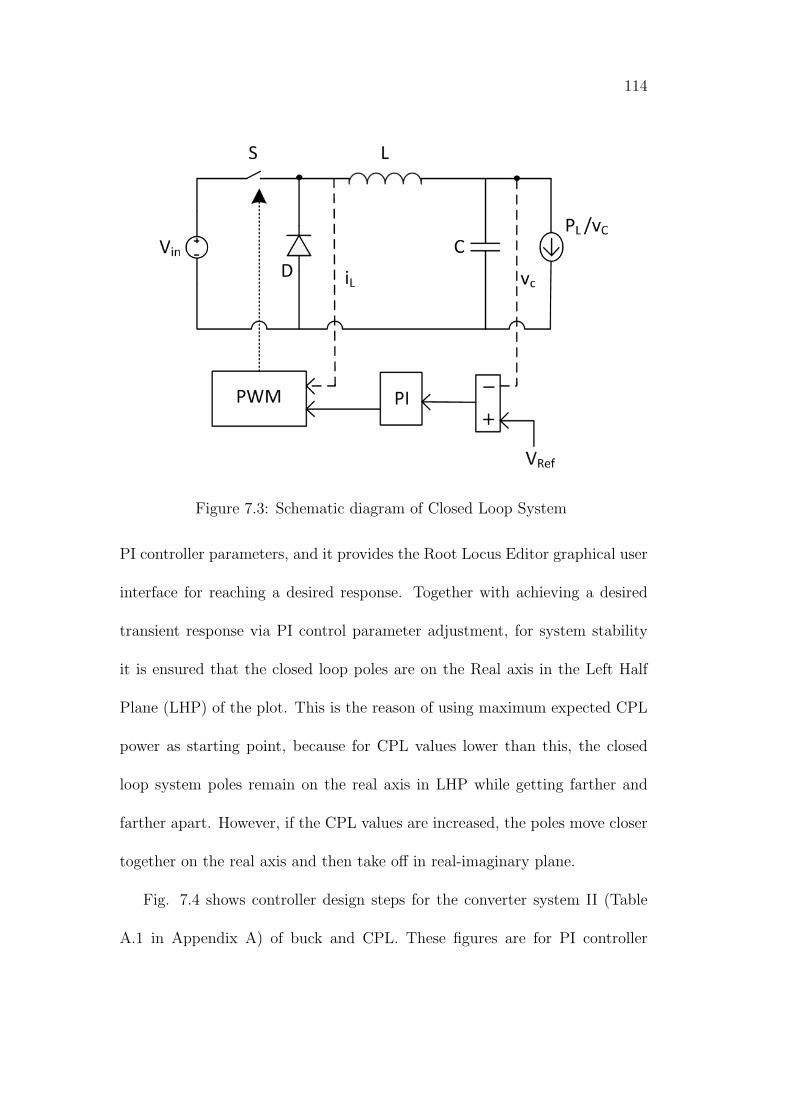
114
Figure 7.3: Schematic diagram of Closed Loop System
PI controller parameters, and it provides the Root Locus Editor graphical user
interface for reaching a desired response. Together with achieving a desired
transient response via PI control parameter adjustment, for system stability
it is ensured that the closed loop poles are on the Real axis in the Left Half
Plane (LHP) of the plot. This is the reason of using maximum expected CPL
power as starting point, because for CPL values lower than this, the closed
loop system poles remain on the real axis in LHP while getting farther and
farther apart. However, if the CPL values are increased, the poles move closer
together on the real axis and then take off in real-imaginary plane.
Fig. 7.4 shows controller design steps for the converter system II (Table
A.1 in Appendix A) of buck and CPL. These figures are for PI controller

115
parameters of P = 0.17209 and I = 7.5971. The switched system simulation is
then carried out using this controller and the system is tested for CPL value
variations. The simulation waveforms are presented in Fig. 7.5. The system
is operating in a stable manner at CPL value of 1000W when at t = 0.4s the
CPL value is increased to 2000W. The system continues to operate in stable
fashion and regains equilibrium with current level raised higher to cater for
higher load. Similar thing happens at t = 0.6s when load is increased from
2000W to 5000W.
However, with the simple PI controller, it is observed that the system is
unable to properly handle a CPL value transition from high to low value. Fig.
7.6 shows this system behavior.
To cater for this problem, a slight modification is made in the system. A
reset mechanism is introduced which resets the integral part of the PI controller
as soon as the system voltage level rises i.e. a CPL transition from high to
low value occurs. A schematic diagram of this control scheme is shown in Fig.
7.7. The switch compares the actual output voltage with a slightly higher
than desired output voltage level (not shown in figure). As soon as the actual
voltage becomes larger than this level (327V), it raises the reset signal and the
integral part of PI controller is thus reset. Consequently, the control signal
falls to zero. As a result the current drops, leading to a voltage drop, and the
transition is effectively converted into a low to high power transition.
It can be observed from the simulation waveforms of this system as shown
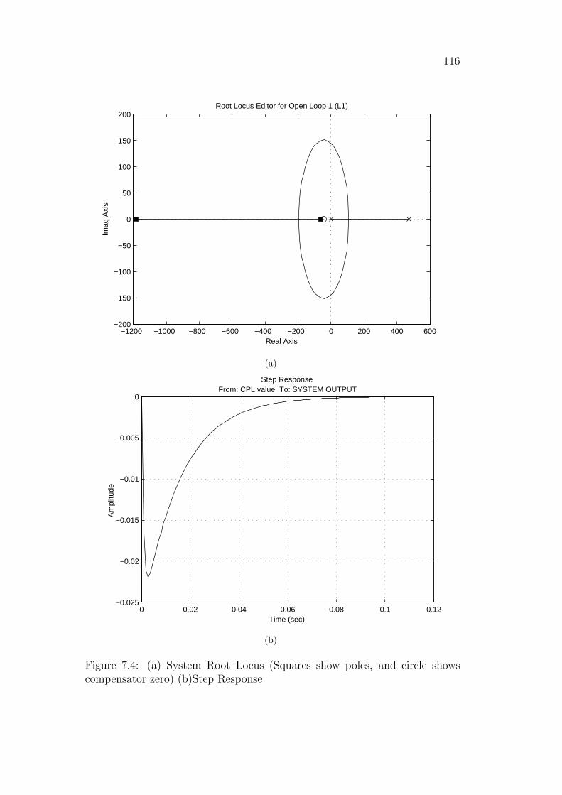
116
−1200 −1000 −800 −600 −400 −200 0 200 400 600−200
−150
−100
−50
0
50
100
150
200
Root Locus Editor for Open Loop 1 (L1)
Real Axis
Imag
Axi
s
(a)
Step Response
Time (sec)
Am
plitu
de
0 0.02 0.04 0.06 0.08 0.1 0.12−0.025
−0.02
−0.015
−0.01
−0.005
0From: CPL value To: SYSTEM OUTPUT
(b)
Figure 7.4: (a) System Root Locus (Squares show poles, and circle showscompensator zero) (b)Step Response
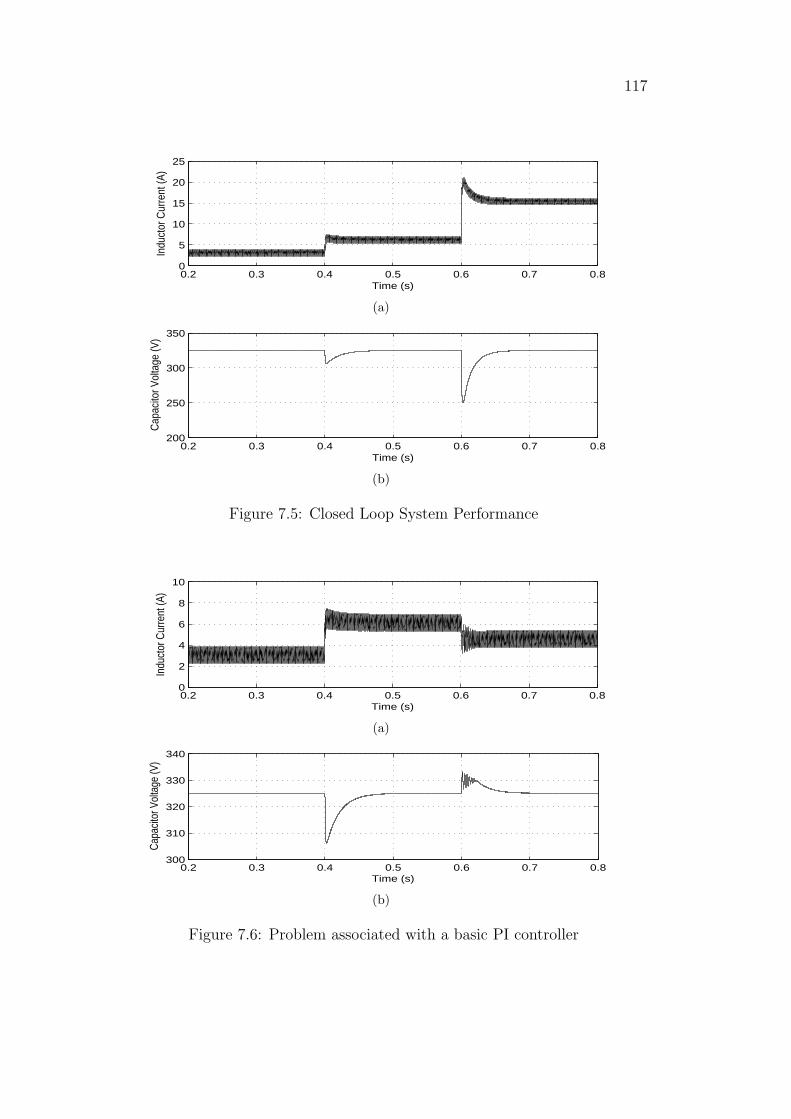
117
0.2 0.3 0.4 0.5 0.6 0.7 0.80
5
10
15
20
25
Time (s)
Indu
ctor
Cur
rent
(A)
(a)
0.2 0.3 0.4 0.5 0.6 0.7 0.8200
250
300
350
Time (s)
Cap
acito
r Vol
tage
(V)
(b)
Figure 7.5: Closed Loop System Performance
0.2 0.3 0.4 0.5 0.6 0.7 0.80
2
4
6
8
10
Time (s)
Indu
ctor
Cur
rent
(A)
(a)
0.2 0.3 0.4 0.5 0.6 0.7 0.8300
310
320
330
340
Time (s)
Capa
citor
Vol
tage
(V)
(b)
Figure 7.6: Problem associated with a basic PI controller
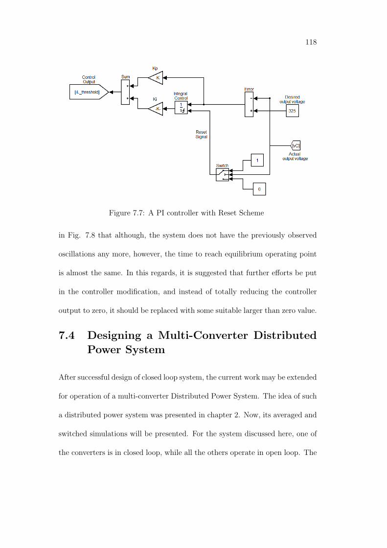
118
Figure 7.7: A PI controller with Reset Scheme
in Fig. 7.8 that although, the system does not have the previously observed
oscillations any more, however, the time to reach equilibrium operating point
is almost the same. In this regards, it is suggested that further efforts be put
in the controller modification, and instead of totally reducing the controller
output to zero, it should be replaced with some suitable larger than zero value.
7.4 Designing a Multi-Converter Distributed
Power System
After successful design of closed loop system, the current work may be extended
for operation of a multi-converter Distributed Power System. The idea of such
a distributed power system was presented in chapter 2. Now, its averaged and
switched simulations will be presented. For the system discussed here, one of
the converters is in closed loop, while all the others operate in open loop. The
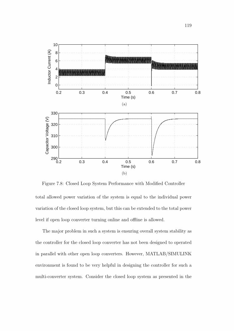
119
0.2 0.3 0.4 0.5 0.6 0.7 0.8
0
2
4
6
8
10
Time (s)
Indu
ctor
Cur
rent
(A
)
(a)
0.2 0.3 0.4 0.5 0.6 0.7 0.8290
300
310
320
330
Time (s)
Cap
acito
r V
olta
ge (
V)
(b)
Figure 7.8: Closed Loop System Performance with Modified Controller
total allowed power variation of the system is equal to the individual power
variation of the closed loop system, but this can be extended to the total power
level if open loop converter turning online and offline is allowed.
The major problem in such a system is ensuring overall system stability as
the controller for the closed loop converter has not been designed to operated
in parallel with other open loop converters. However, MATLAB/SIMULINK
environment is found to be very helpful in designing the controller for such a
multi-converter system. Consider the closed loop system as presented in the
120
previous section with controller parameters P=0.17209 and I=7.5971. This
converter will be used together with three more converter of the same parame-
ter values but working in open loop. The overall power supplied to the load will
thus increase to four times that of the single system i.e. from 5kW to 20kW.
However,the closed loop system with these controller parameters is found to
be unacceptable, with large oscillations in voltage and current, as well as the
shifting of open loop converters to DCM.
To have an insight into this problem, the single converter closed loop system
is analyzed with load equal to total closed loop system load i.e. 20kW. Fig.
7.9 shows the root locus position of the system. The poles are in the Right
Half Plane (RHP) and the step response clearly shows an unstable behavior.
This is one reason why the controller cannot work with the multi-converter
closed loop system.
After this, the single converter system is tested with capacitance equal to
total system capacitance of the multi-converter system i.e. 4𝐶 which is 400𝜇F
(and with load 5kW). Again it is found that the extra capacitance due to the
multi-converter system tends to destabilize the system. The poles move closer
together in LHP and can take off in the imaginary axis.
The technique used here to stabilize the system is to design the controller
for a single converter system with
𝐶𝑃𝐿 𝑣𝑎𝑙𝑢𝑒 = 𝑇𝑜𝑡𝑎𝑙 𝐶𝑃𝐿 𝑙𝑜𝑎𝑑𝑖𝑛𝑔 𝑜𝑓 𝑚𝑢𝑙𝑡𝑖𝑐𝑜𝑛𝑣𝑒𝑟𝑡𝑒𝑟 𝑠𝑦𝑠𝑡𝑒𝑚 (7.1)
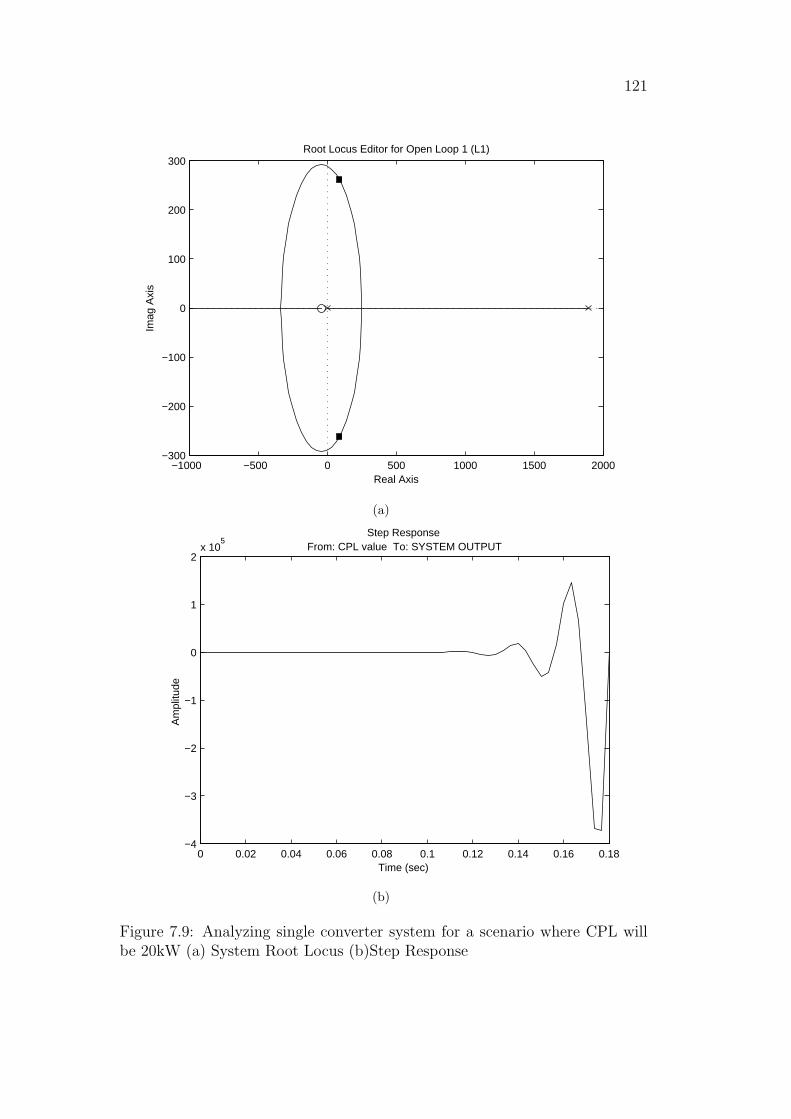
121
−1000 −500 0 500 1000 1500 2000−300
−200
−100
0
100
200
300Root Locus Editor for Open Loop 1 (L1)
Real Axis
Imag
Axi
s
(a)
Step Response
Time (sec)
Am
plitu
de
0 0.02 0.04 0.06 0.08 0.1 0.12 0.14 0.16 0.18−4
−3
−2
−1
0
1
2x 10
5From: CPL value To: SYSTEM OUTPUT
(b)
Figure 7.9: Analyzing single converter system for a scenario where CPL willbe 20kW (a) System Root Locus (b)Step Response
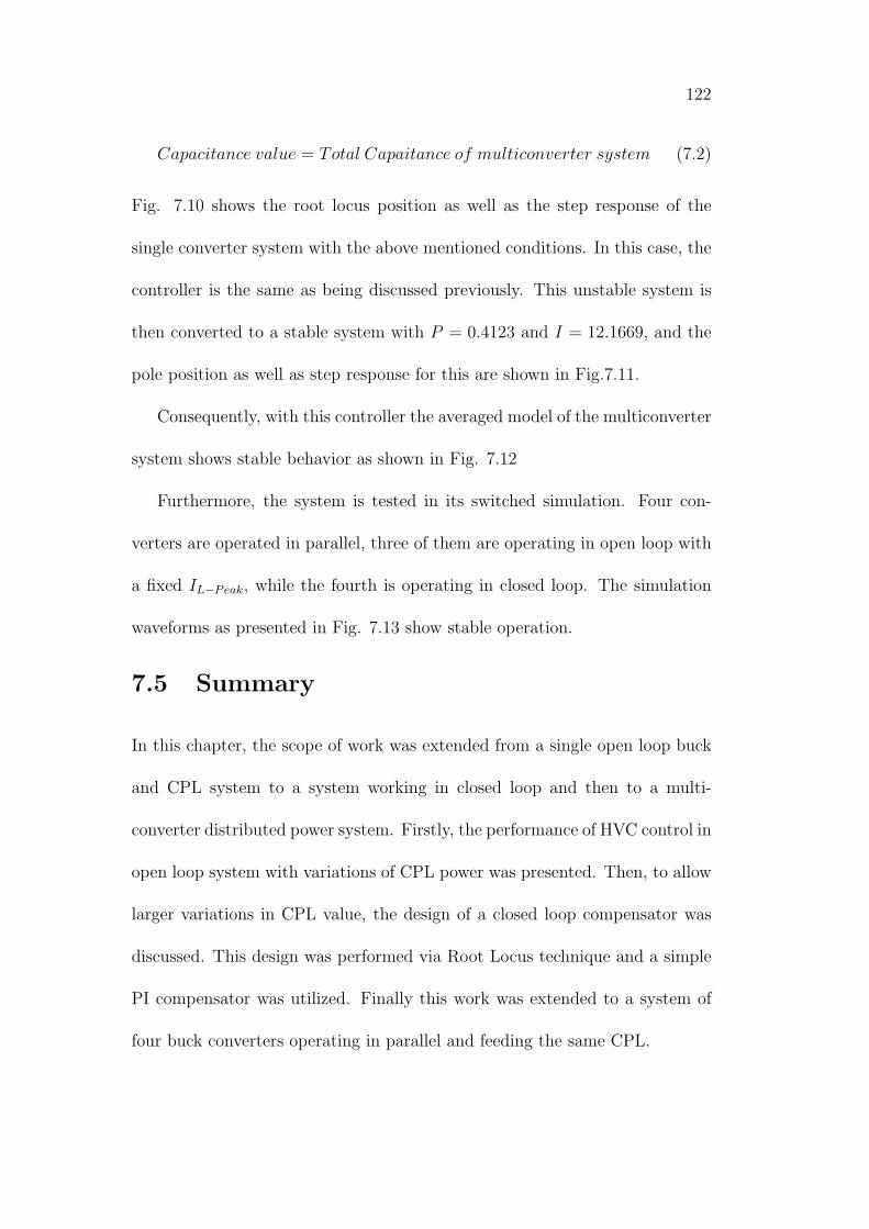
122
𝐶𝑎𝑝𝑎𝑐𝑖𝑡𝑎𝑛𝑐𝑒 𝑣𝑎𝑙𝑢𝑒 = 𝑇𝑜𝑡𝑎𝑙 𝐶𝑎𝑝𝑎𝑖𝑡𝑎𝑛𝑐𝑒 𝑜𝑓 𝑚𝑢𝑙𝑡𝑖𝑐𝑜𝑛𝑣𝑒𝑟𝑡𝑒𝑟 𝑠𝑦𝑠𝑡𝑒𝑚 (7.2)
Fig. 7.10 shows the root locus position as well as the step response of the
single converter system with the above mentioned conditions. In this case, the
controller is the same as being discussed previously. This unstable system is
then converted to a stable system with 𝑃 = 0.4123 and 𝐼 = 12.1669, and the
pole position as well as step response for this are shown in Fig.7.11.
Consequently, with this controller the averaged model of the multiconverter
system shows stable behavior as shown in Fig. 7.12
Furthermore, the system is tested in its switched simulation. Four con-
verters are operated in parallel, three of them are operating in open loop with
a fixed 𝐼𝐿−𝑃𝑒𝑎𝑘, while the fourth is operating in closed loop. The simulation
waveforms as presented in Fig. 7.13 show stable operation.
7.5 Summary
In this chapter, the scope of work was extended from a single open loop buck
and CPL system to a system working in closed loop and then to a multi-
converter distributed power system. Firstly, the performance of HVC control in
open loop system with variations of CPL power was presented. Then, to allow
larger variations in CPL value, the design of a closed loop compensator was
discussed. This design was performed via Root Locus technique and a simple
PI compensator was utilized. Finally this work was extended to a system of
four buck converters operating in parallel and feeding the same CPL.
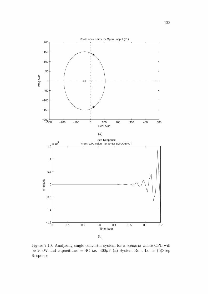
123
−300 −200 −100 0 100 200 300 400 500−200
−150
−100
−50
0
50
100
150
200Root Locus Editor for Open Loop 1 (L1)
Real Axis
Imag
Axi
s
(a)
Step Response
Time (sec)
Am
plitu
de
0 0.1 0.2 0.3 0.4 0.5 0.6 0.7−1.5
−1
−0.5
0
0.5
1
1.5x 10
5From: CPL value To: SYSTEM OUTPUT
(b)
Figure 7.10: Analyzing single converter system for a scenario where CPL willbe 20kW and capacitance = 4C i.e. 400𝜇F (a) System Root Locus (b)StepResponse
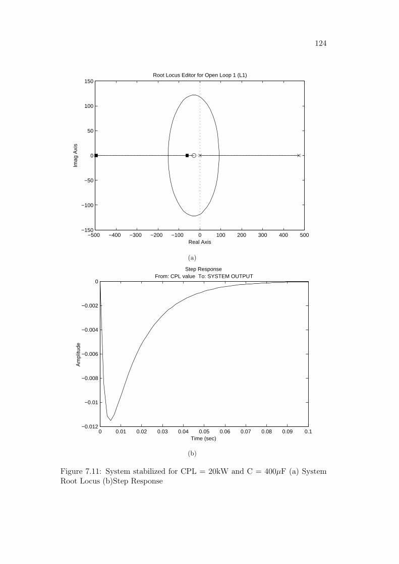
124
−500 −400 −300 −200 −100 0 100 200 300 400 500−150
−100
−50
0
50
100
150Root Locus Editor for Open Loop 1 (L1)
Real Axis
Imag
Axi
s
(a)
Step Response
Time (sec)
Am
plitu
de
0 0.01 0.02 0.03 0.04 0.05 0.06 0.07 0.08 0.09 0.1−0.012
−0.01
−0.008
−0.006
−0.004
−0.002
0From: CPL value To: SYSTEM OUTPUT
(b)
Figure 7.11: System stabilized for CPL = 20kW and C = 400𝜇F (a) SystemRoot Locus (b)Step Response
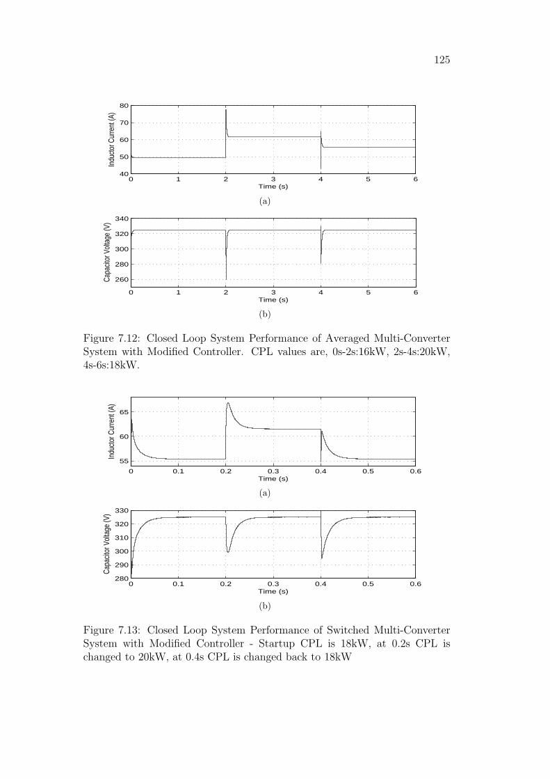
125
0 1 2 3 4 5 640
50
60
70
80
Time (s)
Indu
ctor
Cur
rent
(A)
(a)
0 1 2 3 4 5 6
260
280
300
320
340
Time (s)
Capa
citor
Vol
tage
(V)
(b)
Figure 7.12: Closed Loop System Performance of Averaged Multi-ConverterSystem with Modified Controller. CPL values are, 0s-2s:16kW, 2s-4s:20kW,4s-6s:18kW.
0 0.1 0.2 0.3 0.4 0.5 0.6
55
60
65
Time (s)
Indu
ctor
Cur
rent
(A)
(a)
0 0.1 0.2 0.3 0.4 0.5 0.6280
290
300
310
320
330
Time (s)
Capa
citor
Vol
tage
(V)
(b)
Figure 7.13: Closed Loop System Performance of Switched Multi-ConverterSystem with Modified Controller - Startup CPL is 18kW, at 0.2s CPL ischanged to 20kW, at 0.4s CPL is changed back to 18kW

Chapter 8
Summary and Future Work
This thesis has worked on the idea of dc power distribution. It began with an
introduction of how this paradigm of power distribution was overcome by the
alternating current paradigm years ago, in the early days of electrical power
system. Then, the thesis mentioned that it seems that dc is on the return,
as dc power has found its transformers, which are power electronic converters.
This return of dc is apparent from its presence in three important parts of
a power system namely generation, transmission, and load are witnessing dc
power utilization. However, the last part of the power system where dc has
not shown a significant presence is the distribution system, and the current
work is related to this area.
The thesis presented a number of research efforts related to the idea of
dc power distribution in Chapter 2. The same Chapter presented the ideas
of Distributed Generation and Microgrids and a future dc power distribution
system might be taking benefit from these. Subsequent to this, literature
review was directed towards dc DPS as this system may be a potential future
126
127
dc power distribution system, and the important issue of stability for this
system was addressed.
Chapter 3 presented a comparison of DC power distribution with the AC
paradigm. For the conditions assumed, it was observed that DC has the po-
tential for being a comparable system to AC paradigm. This comparison was
based upon calculating system efficiency and this efficiency is heavily depen-
dent upon the efficiency of power electronic converters used in the DC power
system. In this regard, the Chapter went on to present a technique to cal-
culate minimum required efficiency of power electronic converters in a DC
distribution system that would make it at least as efficient as an equivalent
AC distribution system.
Starting from Chapter 4, the thesis shifted its focus towards the stability
issue of a DC DPS. Chapter 4 presented the technique of HVC control which
allows to operate a buck DC/DC converter feeding a constant power load in
open loop in continuous conduction mode without becoming unstable. In this
regard, the Chapter presented mathematical model based and circuit based
simulation results. In the next chapter, the performance of the system of
buck converter load with a CPL was compared with a naturally oscillating LC
system, and quarter cycle time periods were presented for the buck converter
system. This Chapter i.e. chapter 5 went on to present power transfer portraits
of the system and gave an insight into how HVC control keeps the system from
being unstable.
128
Mathematical expressions for the system were presented in Chapter 6, and
these were based on the idea of energy balance. These expressions were for up-
per voltage peak and minimum required system capacitance. Then in Chapter
7, the single converter based work was upscaled to include more converters and
a small DC DPS was simulated. This work began with designing a closed loop
controller for the system of a single buck converter and CPL. This was then
extended to designing the controller for a system with multiple buck converters
operated in parallel with one of them in closed loop.
8.1 Future Work
With the design and simulation of a stable multi-converter system feeding
constant power load, this system may be extended to the concepts of a DC
Power Distribution System and a DC microgrid.
Fig. 8.1 shows two of the four converters used for the simulation as dis-
cussed in Chapter 7. The input voltage connection (same for all the converters)
is shown by node 1, and the output of all the converters is joined to node 2.
The purpose to present this figure is to show how this work can be extended
for the simulation of a DC Distribution System and/or a DC Microgrid.
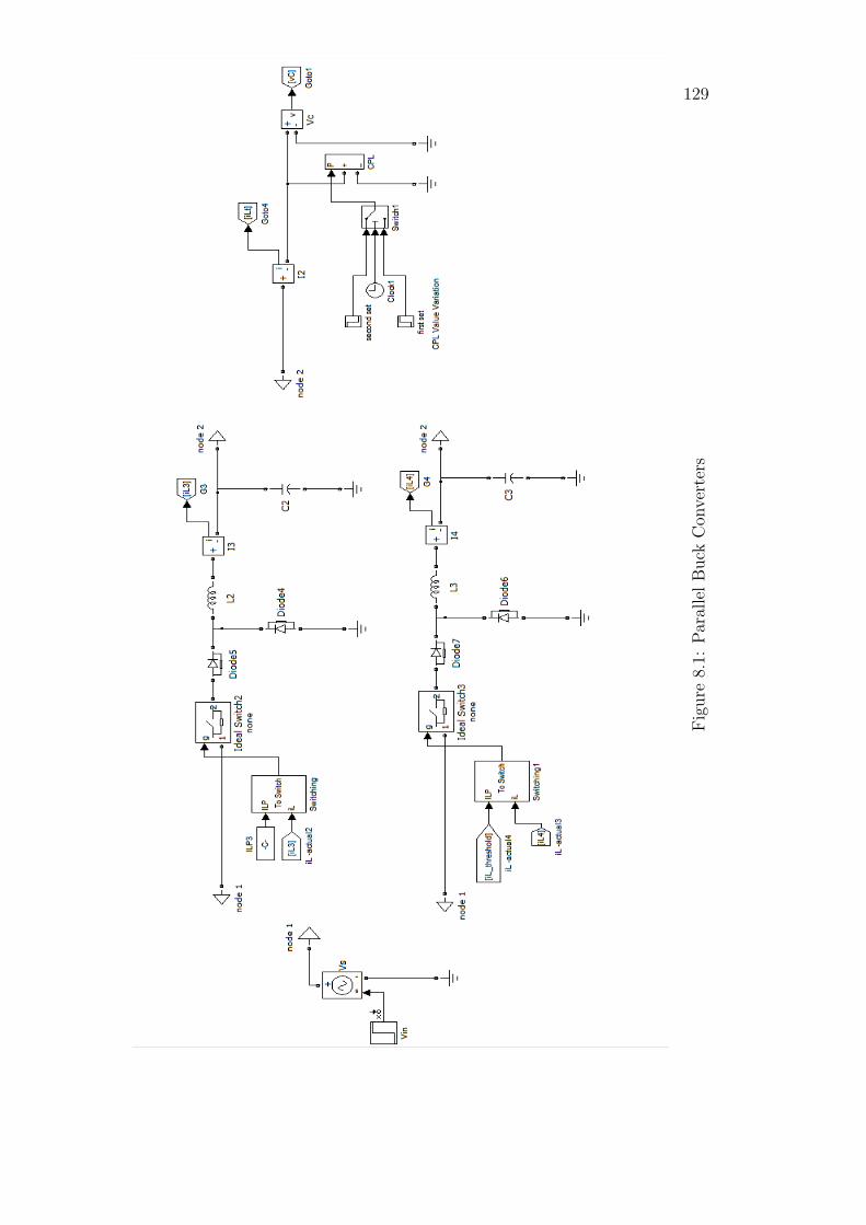
129
Figure
8.1:
ParallelBuck
Con
verters
130
In case of a DC Distribution System or a DC microgrid based upon renew-
able energy based generation, the single 𝑉𝑖𝑛 as shown in the Fig. 8.1 can be
replaced by more 𝑉𝑖𝑛 blocks depending upon the number of renewable sources
being considered. The controller design can be the same, as long as buck
converters are used in the system. However, for a Distribution System, the
Distribution Voltage might be required to be of value higher than that pro-
duced by the sources. This will necessitate the use of boost converters instead
of buck converter. This can be one area of further work for the current effort.
The boost converters will be used to simulate the connection of renewable
sources to the Distribution System, and then on the load side the single CPL as
shown in Fig. 8.1 will be replaced by a parallel combination of buck converters,
which will be basically taking the place of distribution transformers. However,
for such a distribution system, these buck converters alse need to be operating
in closed loop scheme. This will be in order to supply variable power while
maintaining voltage, based upon customer demand. Hence, another extension
to this work, can be to simulate stable parallel system operation with closed
loop buck converters.
Feasibility study of a complete DC distribution system based upon local
DC generation may also be an idea for future work. In this case, an appro-
priate model of the whole system starting from DC generation to the loads
will be simulated. The system efficiency will be calculated and compared to
a counterpart AC system. Alongside this, the life-cycle cost of this system

131
and its components will also be compared with those of a corresponding AC
system. A further comparison will be the stability of the both systems. Based
upon such a study and associated work, a final verdict may be given as to
which of the two systems is better suited for residential power distribution in
the modern day when the concepts of Distributed Generation and Microgrids
are gaining interest and power electronic converters have been developed. A
final verdict may be given that, as far as power distribution is concerned, has
DC won the battle of the currents?
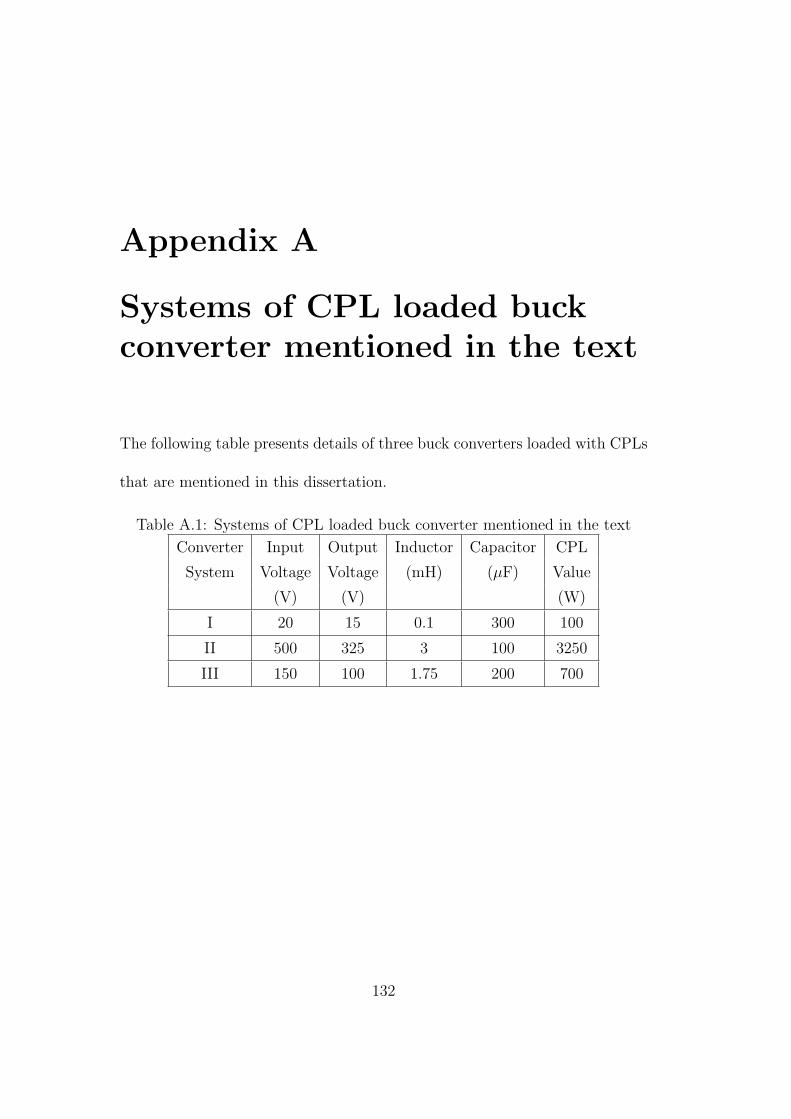
Appendix A
Systems of CPL loaded buckconverter mentioned in the text
The following table presents details of three buck converters loaded with CPLs
that are mentioned in this dissertation.
Table A.1: Systems of CPL loaded buck converter mentioned in the text
Converter Input Output Inductor Capacitor CPL
System Voltage Voltage (mH) (𝜇F) Value
(V) (V) (W)
I 20 15 0.1 300 100
II 500 325 3 100 3250
III 150 100 1.75 200 700
132
Bibliography
[1] F. Dastgeer, A. Kalam, “Efficiency comparison of DC and AC distribu-tion systems for distributed generation”, Australasian Universities PowerEngineering Conference, pp. 1-5, 2009.
[2] C. Sulzberger, “Triumph of ac, part 2 the battle of the currents,” IEEEPower & Energy Magazine, vol. 1, no. 3, pp. 70-73, 2003.
[3] N. Kirby, L. Xu, M. Lucket, W. Spiemann, “HVDC transmission for largeoffshore windfarms,” IET Power Engineering Journal, vol. 16, pp. 135-141,2002.
[4] F. Dastgeer, A. Kalam, “Evolution of dc distributed power system sta-bility”, International Review of Electrical Engineering, part B, vol. 5, pp.652-662, April, 2010.
[5] D. Hammerstrom, “AC versus dc distribution systems did we get it right?”,Power Engineering Society General Meeting, pp. 1-5, June 2007.
[6] K. Engelen, E. Shun, P. Vermeyen, I. Pardon, R. Dhulst, J. Driesen, R.Belmans, “The feasibility of smal-scale residential dc distribution systems,”IEEE Inudustrial Electronics Conference, pp. 2618-2632, Nov. 2006.
[7] M. Starke, L. Tolbert, B. Ozpineci, “AC vs. dc distribution: a loss com-parison”, Transmission and Distribution Conference and Exposition, 2008.T&D. IEEE/PES, pp. 1-7, April 2008.
[8] D. Nilsson, A. Sannino, “Efficiency analysis of low- and medium- voltagedc distribution systems”, Power Engineering Society General Meeting, vol.2, pp. 2315-2321, June 2004.
[9] A. Sannino, G. Postiglione, M. H. J. Bollen, “Feasibility of a dc networkfor commercial facilities”, IEEE Transactions on Industry Applications,vol. 39, Issue 5,pp. 14991507, Sept.-Oct. 2003.
[10] M. Starke, F. Li, L. M. Tolbert, B. Ozpineci, “AC vs. dc distribution:Maximum transfer capability”, Power and Energy Society General Meeting- Conversion and Delivery of Electrical Energy in the 21st Century, pp. 1- 6, July 2008.
133
134
[11] P. Chiradeja, R. Ramakumar, “An approach to quantify the technicalbenefits of distributed generation”, IEEE Transactions on Energy Conver-sion, vol. 19, Issue 4, Dec. 2004.
[12] Z. Jiang, X. Yu, “Hybrid dc- and ac-linked microgrids: Towards inte-gration of distributed energy resources,” IEEE Energy 2030 Conference,2008.
[13] D. Surender, D.K. Jain, A. Kumar, “Power quality issues of embeddedgeneration,” Power India Conference, June 2006.
[14] N. Hadjsaid, J.-F. Canard, F. Dumas, “Dispersed generation impact ondistribution networks,” IEEE Computer Applications in Power, vol. 12, pp.23 - 28.
[15] C.L. Masters, “Voltage rise: the big issue when connecting embeddedgeneration to long 11 kV overhead lines,” Power Engineering Journal, pp.5-12, Feb. 2002.
[16] P. Biczel, “Power electronic converters in dc microgrids,” Fifth Interna-tional Conference-Workshop - CPE 2007, pp. 1 - 6.
[17] C. L. Smallwood, “Distributed generation in autonomous and nonau-tonomous micro grids”, Rural Electric Power Conference, 2002 pp. D1-D1 6.
[18] N. Hatziargyriou, H. Asano, R. Iravani, C. Marnay, “Microgrids anoverview of Ongoing research, development and demonstration projects”,IEEE Power and Energy Magazine, Jul./Aug. 2007.
[19] S. M. T. Bathaee, M. H. Abdollahi, “Fuzzy-neural controller designfor stability enhancement of microgrids” 42nd International UniversitiesPower Engineering Conference, 2007. UPEC 2007, pp. 562-569.
[20] H. Kakigano, Y. Miura, T. Ise, T. Momose, H. Hayakawa, “Fundamen-tal characteristics of dc microgrid for reisdential houses with cogenerationsystem in each house,” Power and Energy Society General Meeting, 2008,pp. 1 - 8.
[21] Y. Zhu, Z. Yin, J. Tian, “Microgrids based on dc energy pool,” IEEEEnergy 2030 Conference, 2008.
[22] A.M. Rahimi, A. Emadi, “Active damping in dc/dc power electronic con-verters: A novel method to overcome the problems of constant powerloads,” IEEE Transactions on Industrial Electronics, vol. 56, pp. 1428-1439, May 2009.
135
[23] E.W. Gholdston, K. Karimi, F.C. Lee, J. Rajagopalan, Y. Panov, B.Manners, “Stability of large dc power systems using switch converters withapplication to the international space station,” Proceedings of the 31stIntersociety Energy Conversion Engineering Conference 1996, pp. 166-171.
[24] C. Rivetta, A. Emadi, G.A. Williamson, R. Jayabalan, B. Fahimi, “Anal-ysis and control of a buck dc-dc converter operating with constant powerload in sea and undersea vehicles, IEEE Industry Applications Conference,2004, vol. 2, pp. 1146-1153.
[25] R.D. Middlebrook, “Input filter considerations in design and applicationsof switching regulators,” IEEE Industry Applications Society Annual Meet-ing Record,1976, pp. 366-382.
[26] I. Lazbin, “Analysis of the stability margins of the space station Free-dom electrical power system,” The 24th Annual IEEE Power ElectronicsSpecialists Conference, 1993.
[27] C.M. Wildrick, F.C. Lee, B.H. Cho, B. Choi, “A method of defining theload impedance specification for a stable distributed power system,” IEEETransaction on Power Electronics, vol. 10, pp. 280-5, May. 1995.
[28] Y. Panov, J. Rajagopalan, F.C. LEE, “Analysis and design of N paralleledDC-DC converters with master-slave current-sharing control,” The 12thAnnual Applied Power Electronics Conference and Exposition, Feb. 23-27,1997.
[29] X. Feng, Z. Ye, K. Xing, F. C. Lee, “Individual load impedance specifica-tion for a stable dc distributed power system,” The 14th Annual AppliedPower Electronics Conference and Exposition, March 1999, pp. 923929.
[30] X. Feng, C. Liu, Z. Ye, F.C Lee, D. Borojevic, “Monitoring the stability ofdc distributed power systems,” The 25th Annual Conference of the IEEEIndustrial Electronics Society, 1999.
[31] V. Grigore, J. Hatonen, J. Kyyra, T. Suntio, “Dynamics of a buck con-verter with a constant power load,” Proc. 29th Annu. IEEE Power Elec-tronics Specialists Conf. 1998, vol. 1, pp. 72-78.
[32] I. Gadoura, V. Grigore, J. Hatonen, J. Kyyra, P. Vallittu, T. Suntio,“Stabilizing a telecom power supply feeding a constant power load,” The20th International Telecommunications Energy Conference, Oct. 1998, SanFrancisco.
136
[33] B. Choi, B. Cho, S. Hong, “Dynamics and control of dc-to-dc convertersdriving other converters downstream,” IEEE Trans. on Circuits and Sys-tems I: Fundamental Theory and Applications, vol. 46, pp. 1240-1248, Oct.1999.
[34] J. Mahdavi, A. Emadi, “Sliding-mode control of PWM Cuk converter,”The 6th International Conference on Power Electronics and Variable SpeedDrives, pp. 372377, 1996.
[35] A. Emadi, M. Ehsani, “Negative impedance stabilizing controls for pwmdc/dc converters using feedback linearization techniques,” The 35th In-tersociety Energy Conversion Engineering Conference and Exhibit, pp.613620, Jul. 2000.
[36] J.G. Ciezki, R.W. Ashton, “The design of stabilizing controls for ship-board dc-to-dc buck choppers using feedback linearization techniques,” The29th Annual IEEE Power Electronics Specialists Conference, May 1998,Fukuoka, Japan.
[37] I. Kondratiev, E. Santi, R. Dougal, G. Veselov, “Synergetic control fordc-dc buck converters with constant power load,” The 35th Annual IEEEPower Electronics Specialists Conference, June 2004.
[38] C. Rivetta, G.A. Williamson, “Large-signal analysis of a dc-dc buck powerconverter operating with constant power load,” The 29th Annual meetingof the IEEE Industrial Electronics Society, Nov. 2003.
[39] C. Rivetta, G.A. Williamson, “Global behavior analysis of a dc-dc boostpower converter operating with constant power load,” Proceedings of the2004 International Symposium on Circuits and Systems, vol. 5, pp. 956959,May 2004.
[40] I. Kondratiev, E. Santi, R. Dougal, “Nonlinear synergetic control for mparallel-connected dc-dc buck converters: Droop current sharing,” The 37thIEEE Power Electronics Specialists Conference, pp. 17, 2006.
[41] I. Kondratiev, R. Dougal, E. Santi, G. Veselov, “Synergetic control form parallel-connected dc-dc buck converters,” The 37th IEEE Power Elec-tronics Specialists Conference, pp. 182- 188, 2004.
[42] I. Kondratiev, E. Santi, R. Dougal, “Robust nonlinear synergetic controlfor m-parallel-connected dc-dc boost converters,” IEEE Power ElectronicsSpecialists Conference, pp. 2222 2228, 2008.
[43] J. Sun, D. Mitchell, M. Greuel, P.T. Krein, R.M. Bass, “Modeling of pwmconverters in discontinuous conduction mode- A reexamination,” The 29thAnnual IEEE Power Electronics Specialists Conference, pp. 615 622, 1998.
137
[44] A. Khaligh, “Realization of parasitics in stability of dcdc converters loadedby constant power loads in advanced multiconverter automotive systems,”IEEE Transactions on Industrial Electronics, vol. 55, pp. 2295 2305, 2008.
[45] A. Khaligh, S. Williamson, A. Emadi, “Control and stabilization of dc/dcbuck-boost converters loaded by constant power loads in vehicular systemsusing a novel digital scheme,” The 12th International Power Electronicsand Motion Control Conference, pp. 1769 1775, 2006.
[46] A. Khaligh, A.M. Rahimi, A. Emadi, “Negative impedance stabilizingpulse adjustment control technique for dc/dc converters operating in dis-continuous conduction mode and driving constant power loads,” IEEETransactions on Vehicular Technology, vol. 56 , n. 4 , Part. 2, pp. 20052016,2007.
[47] A. Khaligh, A.M. Rahimi, A. Emadi, “Modified pulse-adjustment tech-nique to control dc/dc converters driving variable constant-power loads,”IEEE Transactions on Industrial Electronics, vol. 55 , n. 3, pp. 1133 1146,2008.
[48] K. Xing, J. Guo, W. Huang, D. Peng, F.C. Lee, D. Borojevic, “An activebus conditioner for a distributed power system,” The 30th Annual IEEEPower Electronics Specialists Conference, vol. 2, pp. 895900, 1999.
[49] A.M. Rahimi, A. Emadi, “An analytical investigation of dc/dc power elec-tronic converters with constant power loads in vehicular power systems,”IEEE Transactions on Vehicular Technology, vol. 58, n. 6, pp. 2689 2702,2009.
[50] Table US-1. Electricity consumption by end use in U.S.households, 2001. Energy Information Administration. [Online]http://www.eia.doe.gov/emeu/reps/enduse/er01 us tab1.html
[51] F. Dastgeer, A. Kalam, “Operation of an Open Loop Buck Converterin Continuous Conduction Mode Loaded With a Constant Power Load”submitted for publication in International Journal of Engineering, Scienceand Technology, 2011.
[52] B. Holdsworth, C. Woods, Digital Logic Design, 4th edition, Newnes 2002.