Embed Size (px)
Citation preview

JLMN-Journal of Laser Micro/Nanoengineering Vol. 10, No. 2, 2015
124
Direct Laser Writing of A Channel Waveguide in Al2O3:Nd Thin Film
Andrey G. OKHRIMCHUK*1,2,3, Alexey I. KRIKUNOV*4, Yurii A. OBOD*4, and Oleg D. VOLPIAN*4,5
*1 Aston Institute of Photonic Technologies, Aston University, Aston Triangle, Birmingham B4 7ET, UK E-mail: [email protected]
*2 Fiber Optics Research Center of RAS, 38 Vavilova Street, Moscow 1119333, Russia *3 International Center of Laser Technologies, D. Mendeleyev University of Chemical Technology of Russia, Miusskaya Sq.
9, Moscow 125047, Russia *4 Fotron Auto, 3 Vvedensky Street, Moscow 117342, Russia
*5 R&D Stelmakh’s Polyus Institute, 3 Vvedensky Street, 117342, Russia
The femtosecond laser modification of refractive index in amorphous Al2O3:Nd thin film prepared by rf magnetron sputtering is investigated. Modifications of the refractive index in a sample with a single Al2O3:Nd layer and in a sample composed of the Al2O3:Nd layer and SiO2 layer on the top were compared. Advantages arising from addition of the SiO2 layer are shown. The film was patterned in order to form an active waveguide. Waveguide loss and mode composition were investigated experimentally and theoretically. Spectrum and kinetics of luminescence in the region of 1.06 μm were measured. Keywords: Femtosecond laser direct writing; waveguide, thin film, amorphous aluminum oxide.
1. Introduction.
Amorphous aluminum oxide film is known to be excellent host for rare-earth ions and perspective material for active integrated optical applications. Deposition of high optical quality rare-earth-ion-doped Al2O3 films and waveguide patterning has been recently intensively investigated [1-6]. The first Al2O3:Er3+ laser based on a ring waveguide resonator was demonstrated [2]. The most consumable part of such waveguides manufacturing is patterning, which is based on lithography, and it is attractive to replace it with more flexible and cheaper method of waveguide fabrication.
Meantime over the last 15 years femtosecond direct writing technique of waveguide formation in bulk of dielectric crystals and glasses has been extensively developing since the pioneer work devoted to waveguide formation in glasses [7]. Since that time numerous waveguide lasers with different core sizes and shapes have been manufactured by femtosecond laser beam in rare-earth doped glasses [8-9] and crystals [10-16], while only one paper devoted to direct laser writing in a thin film has been published [17].
Here we applied femtosecond laser direct writing technique for waveguide formation in Al2O3:Nd thin film for the first time and consider it as an alternative to lithography as more flexible and quicker method for waveguide patterning. Challenge of femtosecond writing in thin films arises from proximity of the surface and the area, which is to be modified. A non-linear nature of the femtosecond modification leads to dramatic sensitivity to various defects, which are inherent in a surface. In this paper we offer natural solution of this problem by applying an additional film above the modifying film, and thus distancing surface of the sample from the inscribing beam waist.
2. Femtosecond modification of Al2O3:Nd film Amorphous film of Al2O3:Nd with thickness of 1.7
µm was manufactured by rf magnetron reactive sputtering on BK7 glass substrate. The substrate was polished as for laser mirror of a moderate quality, and its roughness was of a few nm (rms). The sputtered target was alloy of Al99.5Nd0.5. Refractive index of the amorphous Al2O3:Nd film was measured with an ellipsometer and found to be 1.574. Such film was used in the first series of inscription experiments. Then an additional layer of SiO2 glass with thickness of 5 µm was applied by the same method on the top of the aluminum oxide film. Thus two kinds of samples with an aluminum oxide film were available for inscription experiments: one had a single Al2O3:Nd film on the BK7 substrate, while the other one consisted of two films, that are the Al2O3:Nd film and the additional SiO2 film on the top.
In laser inscription experiments samples with films were mounted on the Aerotech high precision three-dimensional translation stage. Scanning velocity during laser writing was of 0.5 mm/s. A femtosecond laser beam at wavelength of 800 nm, pulse duration of 110 fs (FWHM) and repetition rate of 1 kHz was focused under surface of the sample at predefined depth h by 100x Mitutoyo lens with numerical aperture NA=0.55. A cylindrical defocusing lens with focal distance of 34 cm was places in front of main focusing Mitutoyo lens and provided a beam waist in a form of highly elongated ellipse in the transverse cross-section. The calculated size of minor ellipse axis was of 1.1 μm, while the major axis size was of 14 μm and the major axis was oriented along an inscribed track.
Inscription threshold for modification of refractive index in Al2O3:Nd film was found be around 0.2 μJ for both samples investigated. Provided that the beam waist
DOI: 10.2961/jlmn.2015.02.0003

JLMN-Journal of Laser Micro/Nanoengineering Vol. 10, No. 2, 2015
125
was positioned below the surface not less then 2 μm, we did not observe sufficient degradation of smoothness of inscribed tracks under pulse energies up to 0.5 μJ in comparison with writing at the threshold pulse energy. Two linear types of polarization were tested, that are perpendicular and parallel to a track, but no differences were found.
Since position of beam waist relative to the Al2O3:Nd film and the surface is obviously critical for writing precisely in the film, series of test tracks were inscribed at different depth h under the surface in range of 2 μm – 15 μm and nearly the same pulse energy around 0.3 μJ. Here the inscription depth is considered as position of hypothetical beam waist relative surface under diffraction limited linear propagation. Refractive index of the medium is assumed to be equal to 1.55 for the sample with single film (which is an average between the parameters for Al2O3:Nd film and BK7 glasses), 1.5 for the sample with two films (which is an average between the parameters for SiO2, Al2O3:Nd films and BK7 glasses).
In experiments with the sample having only the Al2O3:Nd film modification of aluminum oxide film taken place under the inscription depth in range of 0 μm - 7 μm, and under greater depth only modification of the substrate was observed (Fig.1), besides the tracks in the film have got considerably larger roughness than the tracks in the substrate. Such behavior could be explained by increased concentration of defects on the surface, and probably by insufficient homogeneity of the film. It is interesting that the tracks in the film were effectively inscribed with a considerably greater depth range than the film thickness, which could be naturally attributed to high non-linear absorption in the film versus the substrate.
a) b) Fig.1. Microscopic pictures of pairs of tracks inscribed in opposite directions at three different depth h in the sample with the single Al2O3:Nd film. a) the tracks are in the film; b) tracks are in the substrate. Distance between the tracks is 10 μm. The writing beam had linear polarization perpendicular to a track.
Modification of the Al2O3:Nd film with the additional SiO2 film on the top took place under inscription depth in range of 3-7.5 μm under pulse energy of 0.27 µJ (Fig.2), while no tracks were found under the inscription depth less than 3 μm. As in the case of the single film the tracks are efficiently inscribed in the
Al2O3:Nd film with the SiO2 film on the top with a considerably greater depth range than the thickness of the Al2O3:Nd film. In this experiment we have got significantly smoother tracks in the Al2O3:Nd film than in the previous sample without the SiO2 layer.
a) b) c)
d) e) f) Fig.2. Microscopic pictures of track inscribed at three different depths h in the sample with the Al2O3:Nd film and the SiO2 film on top. a), b), c) Top views of pairs of tracks inscribed in opposite directions. Distance between the tracks is of 20 μm; d, e), c) End views of a single track, the Al2O3:Nd is colored in green and has thickness of 1.7 μm. The writing beam had linear polarization parallel to a track.
Refractive index change in tracks inscribed in the Al2O3:Nd film was investigated with QPm method, based on the solution of the so-called transport-of-intensity equation [18]. Setup for measurement was based on Zeiss microscope with back illumination of the sample by the tungsten lamp light passed through interference filter with center wavelength of 530 and FWHM of 5 nm. It was found to be negative with absolute value around 0.01 under inscription pulse energy of 0.3 µJ. 3. Fabrication of waveguide
Ten tracks with depressed refractive index composing waveguide cladding were inscribed at the opposite sides of un-exposed waveguide core to ensure wave confinement in the direction along the films plane (Fig.3). Laser writing setup is described in the previous chapter. Inscription was done in the sample without additional SiO2 film, so roughness of the track was rather large. The sample was cut perpendicular to the waveguide, and then the ends were polished. Waveguide length was 5 mm.
h= 3.1 μm 4.7 μm 11 μm
h= 3.0 μm
4.5 μm 6.0 μm
JLMN-Journal of Laser Micro/Nanoengineering Vol. 10, No. 2, 2015
126
Fig.3. Microscopic picture of the waveguide end in the Al2O3:Nd film. 4. Waveguide characterization
The transmittance spectrum of the waveguide was recorded with the super-continuum fiber source Fianium. Super-continuum laser beam was coupled into the waveguide by a high NA aspheric lens with focal distance of 3.3 mm. The output light was collected in a multimode fiber and transmitted to the Ando spectrum analyzer, model AQ6317B. Transmittance spectrum displays strong modulations due to absorption of Nd3+ ions (Fig.4). The absorption lines demonstrate pronounced inhomogeneous broadening due to amorphous nature of the aluminum oxide film. Absorption band centered at 804 nm is suitable for pumping by laser diodes. Waveguide absorbance due to the Nd3+ dopants at this wavelength is as high as 78 %, and attenuation coefficient equals to 13 dB/cm.
Fig.4. Transmittance spectrum of the waveguide in the Al2O3:Nd film.
Waveguiding properties were characterized with
tunable CW Ti:sapphire laser operating at wavelength of 804 nm. A cylindrical telescope was applied to form an elliptical cross-section of the laser beam with eccentricity close to those of calculated fundamental waveguide mode. Then the laser beam was coupled to waveguide by the mentioned above aspheric lens, and collected by the microscopic lens on a power meter head or on CCD of a laser beam profilometer. Transmittance of the waveguide was found to be 13%. Excluding the loss due to neodymium absorption and Fresnel reflection, we have found that loss due to scattering and leakage in the waveguide could be as high as 3.8 dB/cm. In reality this loss would be lower as we do not take into account coupling loss, and it is included in this value.
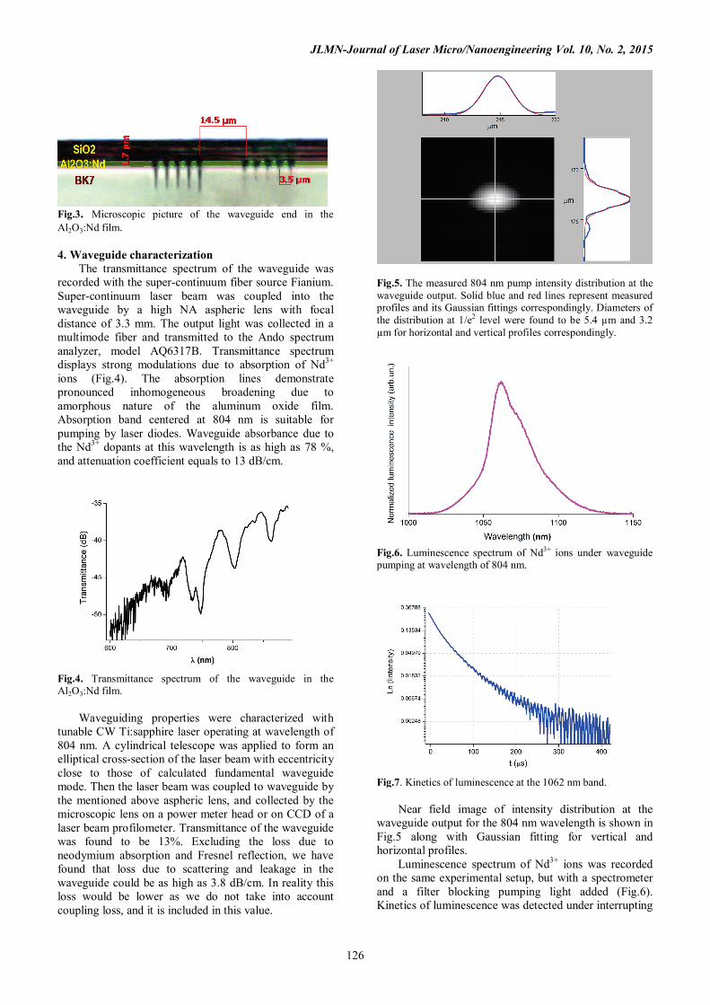
Fig.5. The measured 804 nm pump intensity distribution at the waveguide output. Solid blue and red lines represent measured profiles and its Gaussian fittings correspondingly. Diameters of the distribution at 1/e2 level were found to be 5.4 µm and 3.2 µm for horizontal and vertical profiles correspondingly.
Fig.6. Luminescence spectrum of Nd3+ ions under waveguide pumping at wavelength of 804 nm.
Fig.7. Kinetics of luminescence at the 1062 nm band.
Near field image of intensity distribution at the waveguide output for the 804 nm wavelength is shown in Fig.5 along with Gaussian fitting for vertical and horizontal profiles.
Luminescence spectrum of Nd3+ ions was recorded on the same experimental setup, but with a spectrometer and a filter blocking pumping light added (Fig.6). Kinetics of luminescence was detected under interrupting

JLMN-Journal of Laser Micro/Nanoengineering Vol. 10, No. 2, 2015
127
of a CW pump laser beam by a mechanical chopper (Fig.7). The luminescence exhibits non-exponential behavior with averaged lifetime about of 60 μs.
The measured near field image of luminescence intensity distribution at the waveguide output for 1062 nm wavelength band is shown in Fig.8.
Fig.8. Luminescence intensity distribution at the waveguide output end. Solid blue lines represent measured profiles. Solid red line in the horizontal profile is fitting by three Gaussian profiles corresponding to the fundamental and the 2-nd modes. In vertical profile solid red line represents fitting by one Gaussian contour. Full width of the vertical profile at 1/e2 level was found to be 4.4 µm. 5. Discussions
One should expect mode leakage along the Al2O3:Nd film, because of finite thickness of the cladding consisting of the 10 tracks. Theoretical mode analysis was performed with commercial code Comsol Multiphysics for pump wavelengths of 804 nm and luminescence wavelength of 1062 nm under assumption that refractive index change is constant within a track and equals to -0.01 for both wavelengths. Two leakage modes were found in each case. In Fig.8 mode intensity distribution is shown for 804 nm. The distribution for wavelength of 1062 nm is not shown, because it is very analogous. It was calculated that at pump wavelength of 804 nm the fundamental and second modes have got losses of 0.1 dB/cm and 0.4 dB/cm correspondingly.
Measured pump intensity distribution (Fig.5) fairly corresponds to the simulated fundamental mode. Nevertheless theoretical vertical mode size was found to be equaled to 1.7 μm, which is almost 2 times less than the experimental one equaled to 3.2 μm, and theoretical horizontal mode size is nearly 2.5 times higher than the experimental one (13 μm versus 5.4 μm). The discrepancy in horizontal direction could be due to possible inhomogeneity of refractive index profile within a core that was not taken into account in simulations. Indeed in Fig.1a one could observe performance of mechanical deformations due induced stress around a track inscribed in the Al2O3:Nd film, which relaxes at distance of few microns apart from the track like damped oscillations. Thus refractive index perturbation around cladding tracks in the waveguide could reduce effective core size. Remarkably, there are no such periodical
deformations in the sample with the additional SiO2 layer on the top (Fig.2). We think that the additional SiO2 film suppresses such deformations.
The mode size increase in the vertical direction could be due to imperfections of the boundary between substrate and the film and some variation of film thickness along the waveguide that could cause mode scattering and leakage. These imperfections are also manifested in rather large measured propagation loss, which is higher in comparison with theoretical one. The last takes into account only leakage through cladding in the film, meantime high roughness of tracks composing the waveguide cladding also contributes to propagation loss. However roughness of the tracks is considerably lower for the sample with the additional SiO2 film (compare Fig.1a and Fig.2). This could be the case due to that an additional SiO2 film on the top significantly suppresses destructive interaction of the inscribing beam with imperfect boundaries of the Al2O3:Nd film, and probably diminishes defect density on these boundaries. Thus a waveguide inscribed in the two-layer film is expected to have lower loss. We believe that the extra loss can be also diminished by reduce of substrate roughness and improvement of the rf sputtering process.
a)
b)
Fig.9. Calculated intensities for waveguide modes at wavelength of 804 nm. Refractive index change is assumed to be -0.01. a) fundamental mode; b) 2-nd mode. Both modes are degenerated by polarization. Pictures of modes at wavelength of 1062 nm are very analogous.
It is interesting that for the 2-layer sample no tracks
were found in the sample under the inscription depth less than 3 μm in the range of pulse energies investigated. We explain this in the following way. The beam is focused in the SiO2 film under such depth. Bandgap of SiO2 film (9.3 eV [19]) is remarkably greater than that of amorphous Al2O3 film (~3.2 eV, [20]) and BK7 glass (4.28 eV, [21]), so one should expect greater energy threshold for inscription in the SiO2 film than in Al2O3 film and BK7, and it was not reached in our experimental

JLMN-Journal of Laser Micro/Nanoengineering Vol. 10, No. 2, 2015
128
conditions, while narrow bandgap of Al2O3 film insures modification in it under wide inscription depth h. This effect can be exploited in applications, where fine localization of modified region in direction of the inscription beam is needed.
The luminescence spectrum corresponds to transitions between 4F3/2 and 4I13/2 multiplets. A wide single band centered at 1062 nm with FWHM as high as 32 nm clearly shows inhomogeneous broadening. This is obviously due to multisite positions of Nd ions in frame of the amorphous Al2O3 film. The non-exponential kinetics confirms this statement.
Shape of luminescence intensity distribution at waveguide output end indicates that the luminescence is trapped in the waveguide (Fig.8). It is decomposed into fundamental and 2-nd modes as shown in the Fig.8. 6. Conclusions
Femtosecond direct writing is a promising technique for 2-D patterning of refractive index in the amorphous aluminum oxide thin film. Combined depressed cladding/step index waveguide is fabricated in the Al2O3:Nd thin film. Focusing of the femtosecond laser beam through an additional SiO2 film applied on the top of the Al2O3 film permits to reduce roughness of the inscribed tracks, and should be a solution for fabrication of low loss waveguides based on the Al2O3 film. Acknowledgments This work was supported by Ministry of Education of Science of Russian Federation, grant #14.Z50.31.0009. References [1] J. D. B. Bradley, F. Ay, K. Worhoff, M. Pollnau:
Appl. Phys. B 89, 311-318 (2007). [2] J. D. B. Bradley, R. Stoffer, L. Agazzi, F. Ay, K.
Wörhoff, and M. Pollnau, Optics Letters, 35, 73-75 (2010).
[3] E. H. Bernhardi, H. A.G.M. van Wolferen, L. Agazzi, M. R. H. Khan, C. G.H. Roeloffzen, K. Wörhoff, M. Pollnau, and R. M. de Ridder, Optics Letters, 35, 2394-2396 (2010).
[4] E. H. Bernhardi, H. A.G.M. van Wolferen, K. Wörhoff, R. M. de Ridder, and M. Pollnau, Optics Letters, 36, 603-605 (2011).
[5] J. D. B. Bradley, Purnawirman, E. Shah Hosseini, J. Sun, T. N. Adam, G. Leake, D. Coolbaugh, and M. R. Watts : CLEO-2013, Technical digest, CF11.4.
[6] J. D. B. Bradley, E. S. Hosseini, Purnawirman, Z. Su, T. N. Adam, G. Leake, D. Coolbaugh, and M. R. Watts, Optics Express, 22, 12226 (2014).
[7] K.M. Davis, K. Miura, N. Sugimoto, and K. Hirao, (1996), Optics Letters, 21, 1729-1731 (1996).
[8] S. Taccheo, G. Della Valle, R. Osellame, G. Cerullo, N. Chiodo, P. Laporta, and O. Svelto, Optics Letters, 29, 2626-2628 (2004).
[9] D.G. Lancaster, S. Gross, H. Ebendorff-Haidepriem, K. Kuan, T.M. Monro, M. Ams, A. Fuerbach, and M.J. Withford, Optics Letters, 36, 1587-1589 (2011).
[10] A.G. Okhrimchuk, A.V. Shestakov, I. Khrushchev, and J. Mitchell, Optics Letters, 30, 2248-2250 (2005).
[11] A.H. Nejadmalayeri, P.R. Herman, J. Burghoff, M. Will, S. Nolte, and A. Tünnermann, Optics Letters, 30, 964-966 (2005).
[12] J. Siebenmorgen, T. Calmano, K. Petermann, and G. Huber, Optics Express 18(15), 16035–16041 (2010).
[13] J. R. Macdonald, S. J. Beecher, P. A. Berry, K. L. Schepler, and A. K. Kar, Appl.Phys.Lett., 102, 161110 (2013).
[14] P. A. Berry, J. R. Macdonald, Stephen J. Beecher, S. A. McDaniel, K. L. Schepler, and A. K. Kar, Optical Materials Express, 3, 1250-1258 (2013).
[15] A.G. Okhrimchuk, V.K. Mezentsev, A.V. Shestakov, and I. Bennion: Optics Express, 20, 3834 (2012).
[16] Y. Jia, J. R. V. de Aldana, and F. Chen, Optical Materials Express, 3, 645-650 (2013).
[17] A. Zoubir, M. Richardson, C. Rivero, A. Schulte, C. Lopez, and K. Richardson, Optics Letters, 29, 748-750 (2004).
[18] D. Paganin and K. A. Nugent: Phys. Rev. Lett., 80, P.2586-2589 (1998).
[19] Z.A. Weinberg, G.W. Rubloff, and E. Bassous, Phys.Rev. B, 19, 3107-3117 (1979).
[20] I. Costina, and R. Franchy, Appl.Phys.Lett., 78, 4139 (2001).
[21] .D.J. Little, M. Ams, and M.J. Withford, Optical Materials Express”, 1, 670-677 (2011).
(Received: July 1, 2014, Accepted: January 28, 2015)