Embed Size (px)
Citation preview

Data Book 1 2.00
Direct RDRAM128/144-MBit (256K×16/18×32s)
Overview
The Rambus Direct RDRAM is a general purpose high-performance memory device suitable foruse in a broad range of applications including computer memory, graphics, video, and any otherapplication where high bandwidth and low latency are required.
The 128/144-Mbit Direct Rambus DRAMs (RDRAM) are extremely high-speed CMOS DRAMsorganized as 8M words by 16 or 18 bits. The use of Rambus Signaling Level (RSL) technologypermits 600 MHz to 800 MHz transfer rates while using conventional system and board designtechnologies. Direct RDRAM devices are capable of sustained data transfers at 1.25 ns per twobytes (10 ns per sixteen bytes).
The architecture of the Direct RDRAMs allows the highest sustained bandwidth for multiple,simultaneous randomly addressed memory transactions. The separate control and data buses withindependent row and column control yield over 95% bus efficiency. The Direct RDRAM’s thirty-twobanks support up to four simultaneous transactions.
System oriented features for mobile, graphics and large memory systems include powermanagement, byte masking, and x18 organization. The two data bits in the x18 organization aregeneral and can be used for additional storage and bandwidth or for error correction.
Features
• Highest sustained bandwidth per DRAM device
– 1.6 GB/s sustained data transfer rate– Separate control and data buses for maximized efficiency– Separate row and column control buses for easy scheduling and highest performance– 32 banks: four transactions can take place simultaneously at full bandwidth data rates
• Low latency features
– Write buffer to reduce read latency– 3 precharge mechanisms for controller flexibility– Interleaved transactions
• Advanced power management:
– Multiple low power states allows flexibility in power consumption versus time to transition toactive state
– Power-down self-refresh
• Organization: 1 Kbyte pages and 32 banks, x16/18
– x18 organization allows ECC configurations or increased storage/bandwidth– x16 organization for low cost applications
• Uses Rambus Signaling Level (RSL) for up to 800 MHz operation

Direct RDRAM128/144-MBit (256K×16/18×32s)
Data Book 2 2.00
Figure 1 Direct RDRAM CSP Package
The 128/144-Mbit Direct RDRAMs are offered in a CSP horizontal package suitable for desktop aswell as low-profile add-in card and mobile applications.
Direct RDRAMs operate from a 2.5 V supply.
Table 1 Key Timing Parameters/Part Numbers
Organization I/O Freq.MHz
Trac Part Number
Normal Package:
8M × 18 600 53 ns HYB25R144180C-653
8M × 18 711 45 ns HYB25R144180C-745
8M × 18 800 45 ns HYB25R144180C-845
8M × 18 800 40 ns HYB25R144180C-840
8M × 16 600 53 ns HYB25R128160C-653
8M × 16 711 45 n s HYB25R128160C-745
8M × 16 800 45 ns HYB25R128160C-845
8M × 16 800 40 ns HYB25R128160C-840
Mirror Package:
8M × 18 600 53 ns HYB25M144180C-653
8M × 18 711 45 ns HYB25M144180C-745
8M × 18 800 45 ns HYB25M144180C-845
8M × 18 800 40 ns HYB25M144180C-840
8M × 16 600 53 ns HYB25M128160C-653
8M × 16 711 45 n s HYB25M128160C-745
8M × 16 800 45 ns HYB25M128160C-845
8M × 16 800 40 ns HYB25M128160C-840

Data Book 3 2.00
Direct RDRAM128/144-MBit (256K×16/18×32s)
Pinouts and Definitions
This tables show the pin assignments of the RDRAM package from the top-side of the package (theview looking down on the package as it is mounted on the circuit board). The mechanicaldimensions of this package are shown in a later section. Refer to Section “Center-Bonded FBGAPackage” on page 86. Note - pin #1 is at the A1 position. DQA8/DQB8 are used for 144 Mbit only.They are N.C. for 128Mbit.
Table 2 Normal Package (top view)
Table 3 Mirrored Package (top view)
12 GND – VDD – – – VDD – GND
11 – – – – – – – – –
10 DQA7 DQA4 CFM CFMN RQ5 RQ3 DQB0 DQB4 DQB7
9 GND VDD GND GNDa VDD GND VDD VDD GND
8 CMD DQA5 DQA2 VDDa RQ6 RQ2 DQB1 DQB5 SIO1
7 – – – – – – – – –
6 – – – – – – – – –
5 SCK DQA6 DQA1 VREF RQ7 RQ1 DQB2 DQB6 SIO0
4 VCMOS GND VDD GND GND VDD GND GND VCMOS
3 DQA8 DQA3 DQA0 CTMN CTM RQ4 RQ0 DQB3 DQB8
2 – – – – – – – – –
1 GND – VDD – – – VDD – GND
A B C D E F G H J
12 GND – VDD – – – VDD – GND
11 – – – – – – – – –
10 DQA8 DQA3 DQA0 CTMN CTM RQ4 RQ0 DQB3 DQB8
9 VCMOS GND VDD GND GND VDD GND GND VCMOS
8 SCK DQA6 DQA1 VREF RQ7 RQ1 DQB2 DQB6 SIO0
7 – – – – – – – – –
6 – – – – – – – – –
5 CMD DQA5 DQA2 VDDa RQ6 RQ2 DQB1 DQB5 SIO1
4 GND VDD GND GNDa VDD GND VDD VDD GND
3 DQA7 DQA4 CFM CFMN RQ5 RQ3 DQB0 DQB4 DQB7
2 – – – – – – – – –
1 GND – VDD – – – VDD – GND
A B C D E F G H J

Direct RDRAM128/144-MBit (256K×16/18×32s)
Data Book 4 2.00
Table 4
Signal I/O Type # PinsEdge
# PinsCenter
Description
SIO1,SIO0 I/O CMOS1)
1) All CMOS signals are high-true; a high voltage is a logic one and a low voltage is logic zero.
2 2 Serial input/output. Pins for reading from and writing to the control registers using a serial access protocol. Also used for power management.
CMD I CMOS1) 1 1 Command input. Pins used in conjunction with SIO0 and SIO1 for reading from and writing to the control registers. Also used for power management.
SCK I CMOS1) 1 1 Serial clock input. Clock source used for reading from and writing to the control registers.
VDD – – 14 6 Supply voltage for the RDRAM core and interface logic.
VDDa – – 2 1 Supply voltage for the RDRAM analog circuitry.
VCMOS – – 2 2 Supply voltage for CMOS input/output pins.
GND – – 19 9 Ground reference for RDRAM core and interface.
GNDa – – 2 1 Ground reference for RDRAM analog circuitry.
DQA8 … DQA0 I/O RSL2)
2) All RSL signals are low-true; a low voltage is a logic one and a high voltage is logic zero.
9 9 Data byte A. Nine pins which carry a byte of read or write data between the Channel and the RDRAM. DQA8 is not used by RDRAMs with a x16 organization.
CFM I RSL2) 1 1 Clock from master. Interface clock used for receiving RSL signals from the Channel. Positive polarity.
CFMN I RSL2) 1 1 Clock from master. Interface clock used for receiving RSL signals from the Channel. Negative polarity
VREF 1 1 Logic threshold reference voltage for RSL signals
CTMN I RSL2) 1 1 Clock to master. Interface clock used for transmitting RSL signals to the Channel. Negative polarity.
CTM I RSL2) 1 1 Clock to master. Interface clock used for transmitting RSL signals to the Channel. Positive polarity.
RQ7 … RQ5 orROW2 … ROW0
I RSL2) 3 3 Row access control. Three pins containing control and address information for row accesses.
RQ4 … RQ0 orCOL4 … COL0
I RSL2) 5 5 Column access control. Five pins containing control and address information for column accesses.
DQB8 … DQB0 I/O RSL2) 9 9 Data byte B. Nine pins which carry a byte of read or write data between the Channel and the RDRAM. DQB8 is not used by RDRAMs with a x16 organization.
Total pin count per package 74 54 –
Data Book 5 2.00
Direct RDRAM128/144-MBit (256K×16/18×32s)
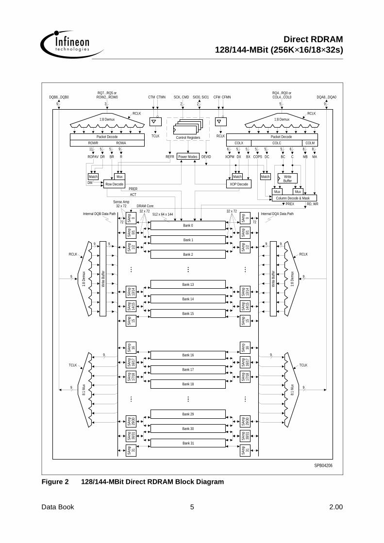
Figure 2 128/144-MBit Direct RDRAM Block Diagram
SPB04206
1:8 Demux
Packet Decode
ROWAROWR
11 5 5 9
TCLK Control Registers
RCLK
CTM CTMN
RCLK
CFM CFMN
8
Packet Decode
COLC
5 5
COLM
865
COLX
6 5 5
XOPM DX
XOP Decode
Match Match WriteBuffer
Mux Mux
Column Decode & Mask
Match Mux
Row Decode
1:8 Demux
RCLK
Power Modes DEVIDREFR
1:8
Dem
ux
RCLK
Writ
e Bu
ffer
9
Bank 0
SAm
p0
0/1
SAm
p
Bank 1
SAm
p1/
2
Bank 2
Bank 13
SAm
p13
/14
Bank 14
SAm
p14
/15
Bank 15
SAm
p15
Bank 16
SAm
p16
/17
Bank 17
SAm
p17
/18
Bank 18
SAm
p
Bank 29
SAm
p29
/30
Bank 30
SAm
p30
/31
Bank 31
SAm
p31
BX COPS DC BC C MB MARBRDRROPAV
PRER
ACT
PREX RD, WR
SAm
p0
SAm
p0/
1SA
mp
1/2
SAm
p13
/14
SAm
p14
/15
SAm
p15
SAm
p16
/17
SAm
p17
/18
SAm
p16
SAm
p29
/30
SAm
p30
/31
SAm
p31
9
8:1
Mux
9
9
1:8
Dem
ux
Writ
e Bu
ffer
8:1
Mux
9 9
9 9
9
9
72 72
Sense Amp32 x 72
32 x 72 32 x 72DRAM Core
512 x 64 x 144
39
DQB8...DQB0 ROW2...ROW0RQ7...RQ5 or
22
RQ4...RQ0 orCOL4...COL0
5
DQA8...DQA0
9
DM
TCLK
RCLK
TCLK
Internal DQB Data Path Internal DQA Data Path
16
SCK, CMD SIO0, SIO1

Direct RDRAM128/144-MBit (256K×16/18×32s)
Data Book 6 2.00
General Description
Figure 2 is a block diagram of the 128/144 Mbit Direct RDRAM. It consists of two major blocks: a“core” block built from banks and sense amps similar to those found in other types of DRAM, and aDirect Rambus interface block which permits an external controller to access this core at up to1.6 GB/s.
Control Registers: The CMD, SCK, SIO0, and SIO1 pins appear in the upper center of Figure 2.They are used to write and read a block of control registers. These registers supply the RDRAMconfiguration information to a controller and they select the operating modes of the device. The ninebit REFR value is used for tracking the last refreshed row. Most importantly, the five bit DEVIDspecifies the device address of the RDRAM on the Channel.
Clocking: The CTM and CTMN pins (Clock-To-Master) generate TCLK (Transmit Clock), theinternal clock used to transmit read data. The CFM and CFMN pins (Clock-From-Master) generateRCLK (Receive Clock), the internal clock signal used to receive write data and to receive the ROWand COL pins.
DQA, DQB Pins: These 18 pins carry read (Q) and write (D) data across the Channel. They aremultiplexed/de-multiplexed from/to two 72-bit data paths (running at one-eighth the data frequency)inside the RDRAM.
Banks: The 16 Mbyte core of the RDRAM is divided into 32 0.5 Mbyte banks, each organized as512 rows, with each row containing 64 dualocts, and each dualoct containing 16 bytes. A dualoct isthe smallest unit of data that can be addressed.
Sense Amps: The RDRAM contains 34 sense amps. Each sense amp consists of 512 bytes of faststorage (256 for DQA and 256 for DQB) and can hold one-half of one row of one bank of theRDRAM. The sense amp may hold any of the 512 half-rows of an associated bank. However, eachsense amp is shared between two adjacent banks of the RDRAM (except for numbers 0, 15, 30, and31). This introduces the restriction that adjacent banks may not be simultaneously accessed.
RQ Pins: These pins carry control and address information. They are broken into two groups.RQ7 … RQ5 are also called ROW2 … ROW0, and are used primarily for controlling row accesses.RQ4 … RQ0 are also called COL4 … COL0, and are used primarily for controlling columnaccesses.
ROW Pins: The principle use of these three pins is to manage the transfer of data between thebanks and the sense amps of the RDRAM. These pins are de-multiplexed into a 24-bit ROWA(row-activate) or ROWR (row-operation) packet.
COL Pins: The principle use of these five pins is to manage the transfer of data between theDQA/DQB pins and the sense amps of the RDRAM. These pins are de-multiplexed into a 23-bitCOLC (column-operation) packet and either a 17-bit COLM (mask) packet or a 17-bit COLX(extended-operation) packet.
ACT Command: An ACT (activate) command from an ROWA packet causes one of the 512 rowsof the selected bank to be loaded to its associated sense amps (two 256 byte sense amps for DQAand two for DQB).
PRER Command: A PRER (precharge) command from an ROWR packet causes the selectedbank to release its two associated sense amps, permitting a different row in that bank to beactivated, or permitting adjacent banks to be activated.

Data Book 7 2.00
Direct RDRAM128/144-MBit (256K×16/18×32s)
RD Command: The RD (read) command causes one of the 64 dualocts of one of the sense ampsto be transmitted on the DQA/DQB pins of the Channel.
WR Command: The WR (write) command causes a dualoct received from the DQA/DQB data pinsof the Channel to be loaded into the write buffer. There is also space in the write buffer for the BCbank address and C column address information. The data in the write buffer is automatically retired(written with optional bytemask) to one of the 64 dualocts of one of the sense amps during asubsequent COP command. A retire can take place during a RD, WR, or NOCOP to another device,or during a WR or NOCOP to the same device. The write buffer will not retire during a RD to thesame device. The write buffer reduces the delay needed for the internal DQA/DQB data path turn-around.
PREC Precharge: The PREC, RDA and WRA commands are similar to NOCOP, RD and WR,except that a precharge operation is performed at the end of the column operation. Thesecommands provide a second mechanism for performing precharge.
PREX Precharge: After a RD command, or after a WR command with no byte masking (M = 0), aCOLX packet may be used to specify an extended operation (XOP). The most important XOPcommand is PREX. This command provides a third mechanism for performing precharge.
Packet Format
Figure 3 shows the formats of the ROWA and ROWR packets on the ROW pins. Table 5 describesthe fields which comprise these packets. DR4T and DR4F bits are encoded to contain both the DR4device address bit and a framing bit which allows the ROWA or ROWR packet to be recognized bythe RDRAM.
The AV (ROWA/ROWR packet selection) bit distinguishes between the two packet types. Both theROWA and ROWR packet provide a five bit device address and a five bit bank address. An ROWApacket uses the remaining bits to specify a nine bit row address, and the ROWR packet uses theremaining bits for an eleven bit opcode field. Note the use of the “RsvX” notation to reserve bits forfuture address field extension.
Figure 3 also shows the formats of the COLC, COLM, and COLX packets on the COL pins. Table 6describes the fields which comprise these packets.
Table 5 Field Description for ROWA Packet and ROWR Packet
Field Description
DR4T, DR4F Bits for framing (recognizing) a ROWA or ROWR packet. Also encodes highest device address bit.
DR3 … DR0 Device address for ROWA or ROWR packet.
BR4 … BR0 Bank address for ROWA or ROWR packet. RsvB denotes bits ignored by the RDRAM.
AV Selects between ROWA packet (AV = 1) and ROWR packet (AV = 0).
R8 … R0 Row address for ROWA packet. RsvR denotes bits ignored by the RDRAM.
ROP10 … ROP0 Opcode field for ROWR packet. Specifies precharge, refresh, and power management functions.

Direct RDRAM128/144-MBit (256K×16/18×32s)
Data Book 8 2.00
The COLC packet uses the S (Start) bit for framing. A COLM or COLX packet is aligned with thisCOLC packet, and is also framed by the S bit.
The 23 bit COLC packet has a five bit device address, a five bit bank address, a six bit columnaddress, and a four bit opcode. The COLC packet specifies a read or write command, as well assome power management commands.
The remaining 17 bits are interpreted as a COLM (M = 1) or COLX (M = 0) packet. A COLM packetis used for a COLC write command which needs bytemask control. The COLM packet is associatedwith the COLC packet from a time tRTR earlier. An COLX packet may be used to specify anindependent precharge command. It contains a five bit device address, a five bit bank address, anda five bit opcode. The COLX packet may also be used to specify some housekeeping and powermanagement commands. The COLX packet is framed within a COLC packet but is not otherwiseassociated with any other packet.
Table 6 Field Description for COLC Packet, COLM Packet, and COLX Packet
Field Description
S Bit for framing (recognizing) a COLC packet, and indirectly for framing COLM and COLX packets.
DC4 … DC0 Device address for COLC packet.
BC4 … BC0 Bank address for COLC packet. RsvB denotes bits reserved for future extension (controller drives 0’s).
C5 … C0 Column address for COLC packet. RsvC denotes bits ignored by the RDRAM.
COP3 …COP0
Opcode field for COLC packet. Specifies read, write, precharge, and power management functions.
M Selects between COLM packet (M = 1) and COLX packet (M = 0).
MA7 … MA0 Bytemask write control bits. 1 = write, 0 = no-write. MA0 controls the earliest byte on DQA8 … 0.
MB7 … MB0 Bytemask write control bits. 1 = write, 0 = no-write. MB0 controls the earliest byte on DQB8 … 0.
DX4 … DX0 Device address for COLX packet.
BX4 … BX0 Bank address for COLX packet. RsvB denotes bits reserved for future extension (controller drives 0’s).
XOP4 …XOP0
Opcode field for COLX packet. Specifies precharge, IOL control, and power management functions.

Data Book 9 2.00
Direct RDRAM128/144-MBit (256K×16/18×32s)
Figure 3 Packet Formats
PREX (d0)MSK (b1)
COLM Packet
T10
The COLM is associated with a previous COLC, and is alignedwith the present COLC, indicated by the Start bit (S = 1) position.
COL0
a)
COL1
MB5
MB6
MB2
MB3 MB0
COL2
COL3
COL4
CTM/CFM
MB7
M = 1 MA6
MB4 MB1
MA4 MA2
S=1a MA7 MA5 MA3
T8
COL0 DC0
COL1
COL2
DC1
DC2
COP3COP2
T9
COP0
COP1
The COLX is aligned with the present COLC,indicated by the Start bit (S = 1) position.
COL0
b)
COL1
XOP0
XOP1
DX0
DX1 BX2
SPB04207
S=1
M = 0MA0
MA1
COL2
COL3
CTM/CFM
COL4
C0BC0BC3
T11
BC4 BC1
RsvB BC2
C1
C2
T12
DQA8...0DQB8...0
BX1
BX0
XOP2
XOP3
DX2
DX3
BX3
BX4
XOP4DX4b RsvB
COLX Packet
T13 T14 T15
ROWA Packet
T2
COLC Packet
T2T0
COL3
COL4
DC3
DC4
CTM/CFM
S = 1
T1
ROW1
ROW0 DR3
DR4F
ROW2
CTM/CFM
DR4T
BR2DR0
DR1 BR1
AV=1RsvB
BR4 RsvR
DR2 BR0 BR3 RsvR
T0 T1
DR2
DR0
DR1
C5
RsvC
C3
C4
T3
COL4...COL0
ROW2...ROW0
CTM/CFM
R3R6
R7 R4
R0
R1
R8 R5 R2
ROW1
ROW0 DR3
DR4F
CTM/CFM
ROW2 DR4T
PRER c0
tPacket
WR b1
ACT a0
T2T0 T1 T3 T4 T7T5 T6 T8 T9 T14T12T10 T11 T13 T15
ROP8
ROP7
ROP6RsvB
4RsvB
BR2
BR1
AV=0
ROP9
BR3BR0 ROP10
ROP1
ROP0ROP3
ROP4
ROP2ROP5
T3 T8
ROWR Packet
T9 T10 T11

Direct RDRAM128/144-MBit (256K×16/18×32s)
Data Book 10 2.00
Field Encoding Summary
Table 7 shows how the six device address bits are decoded for the ROWA and ROWR packets.The DR4T and DR4F encoding merges a fifth device bit with a framing bit. When neither bit isasserted, the device is not selected. Note that a broadcast operation is indicated when both bits areset. Broadcast operation would typically be used for refresh and power management commands. Ifthe device is selected, the DM (DeviceMatch) signal is asserted and an ACT or ROP command isperformed.
Table 8 shows the encodings of the remaining fields of the ROWA and ROWR packets. An ROWApacket is specified by asserting the AV bit. This causes the specified row of the specified bank of thisdevice to be loaded into the associated sense amps.
An ROWR packet is specified when AV is not asserted. An 11 bit opcode field encodes a commandfor one of the banks of this device. The PRER command causes a bank and its two associatedsense amps to precharge, so another row or an adjacent bank may be activated. The REFA(refresh-activate) command is similar to the ACT command, except the row address comes from aninternal register REFR, and REFR is incremented at the largest bank address. The REFP (refresh-precharge) command is identical to a PRER command.
The NAPR, NAPRC, PDNR, ATTN, and RLXR commands are used for managing the powerdissipation of the RDRAM and are described in more detail in “Power State Management” onpage 58. The TCEN and TCAL commands are used to adjust the output driver slew rate and theyare described in more detail in “Current and Temperature Control” on page 65.
Table 7 Device Field Encodings for ROWA Packet and ROWR Packet
DR4T DR4F Device Selection Device Match Signal (DM)
1 1 All devices (broadcast) DM is set to 1
0 1 One device selected DM is set to 1 if DEVID4 … DEVID0 == 0, DR3 … DR0 else DM is set to 0
1 0 One device selected DM is set to 1 if DEVID4 … DEVID0 == 1, DR3 … DR0 else DM is set to 0
0 0 No packet present DM is set to 0

Data Book 11 2.00
Direct RDRAM128/144-MBit (256K×16/18×32s)
Table 9 shows the COP field encoding. The device must be in the ATTN power state in order toreceive COLC packets. The COLC packet is used primarily to specify RD (read) and WR (write)commands. Retire operations (moving data from the write buffer to a sense amp) happenautomatically. See Figure 17 for a more detailed description.
The COLC packet can also specify a PREC command, which precharges a bank and its associatedsense amps. The RDA/WRA commands are equivalent to combining RD/WR with a PREC. RLXC(relax) performs a power mode transition. See “Power State Management” on page 58.
Table 8 ROWA Packet and ROWR Packet Field Encodings
DM1) AV ROP10…ROP0 Field Name Command Description
10 9 8 7 6 5 4 3 2:0
0 - - - - - - - - - --- - No operation.
1 1 Row address ACT Activate row R8 … R0 of bank BR4 … BR0 of device and move device to ATTN2).
1 0 1 1 0 0 0 x3) x x 000 PRER Precharge bank BR4 … BR0 of this device.
1 0 0 0 0 1 1 0 0 x 000 REFA Refresh (activate) row REFR8 … REFR0 of bank BR3 … BR0 of device.Increment REFR if BR4 … BR0 = 1111 (see Figure 50).
1 0 1 0 1 0 1 0 0 x 000 REFP Precharge bank BR4 … BR0 of this device after REFA (see Figure 50).
1 0 x x 0 0 0 0 1 x 000 PDNR Move this device into the powerdown (PDN) power state (see Figure 47).
1 0 x x 0 0 0 1 0 x 000 NAPR Move this device into the nap (NAP) power state (see Figure 47).
1 0 x x 0 0 0 1 1 x 000 NAPRC Move this device into the nap (NAP) power state conditionally.
1 0 x x x x x x x 0 000 ATTN2) Move this device into the attention (ATTN) power state (see Figure 45).
1 0 x x x x x x x 1 000 RLXR Move this device into the standby (STBY) power state (see Figure 46).
1 0 0 0 0 0 0 0 0 x 001 TCAL Temperature calibrate this device (see Figure 52).
1 0 0 0 0 0 0 0 0 x 010 TCEN Temperature calibrate/enable this device (see Figure 52).
1 0 0 0 0 0 0 0 0 0 000 NOROP No operation.
1) The DM (Device Match signal) value is determined by the DR4T,DR4F, DR3 … DR0 field of the ROWA andROWR packets. See Table 7.
2) The ATTN command does not cause a RLX-to-ATTN transition for a broadcast operation (DR4T/DR4F = 1/1).3) An “x” entry indicates which commands may be combined. For instance, the three commands
PRER/NAPRC/RLXR may be specified in one ROP value (011000111000).

Direct RDRAM128/144-MBit (256K×16/18×32s)
Data Book 12 2.00
Table 9 COLC Packet Field Encodings
S DC4 … DC0(select device) 1)
COP3 … 0 Name Command Description
0 ---- ----- – No operation.
1 /= (DEVID4 … 0) ----- – Retire write buffer of this device.
1 == (DEVID4 … 0) x0002) NOCOP Retire write buffer of this device.
1 == (DEVID4 … 0) x001 WR Retire write buffer of this device, then write column C5 … C0 of bank BC4 … BC0 to write buffer.
1 == (DEVID4 … 0) x010 RSRV Reserved, no operation.
1 == (DEVID4 … 0) x011 RD Read column C5 … C0 of bank BC4 … BC0 of this device.
1 == (DEVID4 … 0) x100 PREC Retire write buffer of this device, then precharge bank BC4 … BC0 (see Figure 14).
1 == (DEVID4 … 0) x101 WRA Same as WR, but precharge bank BC4 … BC0 after write buffer (with new data) is retired.
1 == (DEVID4 … 0) x110 RSRV Reserved, no operation.
1 == (DEVID4 … 0) x111 RDA Same as RD, but precharge bank BC4 … BC0 afterward.
1 == (DEVID4 … 0) 1xxx RLXC Move this device into the standby (STBY) power state (see Figure 46).
1) “/=” means not equal, “==” means equal.2) An “x” entry indicates which commands may be combined. For instance, the two commands WR/RLXC may
be specified in one COP value (1001).

Data Book 13 2.00
Direct RDRAM128/144-MBit (256K×16/18×32s)
Table 10 shows the COLM and COLX field encodings. The M bit is asserted to specify a COLMpacket with two 8 bit bytemask fields MA and MB. If the M bit is not asserted, an COLX is specified.It has device and bank address fields, and an opcode field. The primary use of the COLX packet isto permit an independent PREX (precharge) command to be specified without consuming controlbandwidth on the ROW pins. It is also used for the CAL (calibrate) and SAM (sample) current controlcommands (see “Current and Temperature Control” on page 65), and for the RLXX power modecommand (see “Power State Management” on page 58).
Table 10 COLM Packet and COLX Packet Field Encodings
M DX4 … DX0(selects device)
XOP4 …0
Name Command Description
1 ---- – MSK MB/MA bytemasks used by WR/WRA.
0 /= (DEVID4 … 0) – – No operation.
0 == (DEVID4 … 0) 00000 NOXOP No operation.
0 == (DEVID4 … 0) 1xxx01)
1) An “x” entry indicates which commands may be combined. For instance, the two commands PREX/RLXX maybe specified in one XOP value (10010).
PREX Precharge bank BX4 … BX0 of this device (see Figure 14).
0 == (DEVID4 … 0) x10x0 CAL Calibrate (drive) IOL current for this device (see Figure 51).
0 == (DEVID4 … 0) x11x0 CAL/SAM Calibrate (drive) and Sample (update) IOL current for this device (see Figure 51).
0 == (DEVID4 … 0) xxx10 RLXX Move this device into the standby (STBY) power state (see Figure 46).
0 == (DEVID4 … 0) xxxx1 RSRV Reserved, no operation.
Direct RDRAM128/144-MBit (256K×16/18×32s)
Data Book 14 2.00
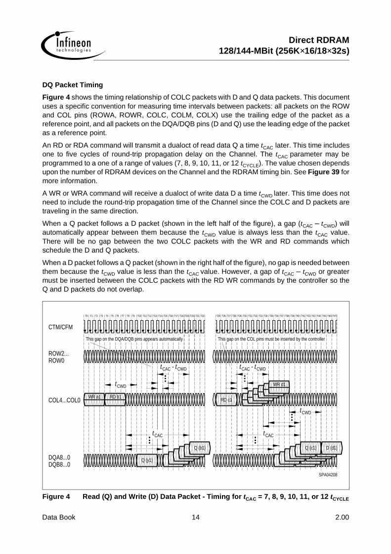
DQ Packet Timing
Figure 4 shows the timing relationship of COLC packets with D and Q data packets. This documentuses a specific convention for measuring time intervals between packets: all packets on the ROWand COL pins (ROWA, ROWR, COLC, COLM, COLX) use the trailing edge of the packet as areference point, and all packets on the DQA/DQB pins (D and Q) use the leading edge of the packetas a reference point.
An RD or RDA command will transmit a dualoct of read data Q a time tCAC later. This time includesone to five cycles of round-trip propagation delay on the Channel. The tCAC parameter may beprogrammed to a one of a range of values (7, 8, 9, 10, 11, or 12 tCYCLE). The value chosen dependsupon the number of RDRAM devices on the Channel and the RDRAM timing bin. See Figure 39 formore information.
A WR or WRA command will receive a dualoct of write data D a time tCWD later. This time does notneed to include the round-trip propagation time of the Channel since the COLC and D packets aretraveling in the same direction.
When a Q packet follows a D packet (shown in the left half of the figure), a gap (tCAC – tCWD) willautomatically appear between them because the tCWD value is always less than the tCAC value.There will be no gap between the two COLC packets with the WR and RD commands whichschedule the D and Q packets.
When a D packet follows a Q packet (shown in the right half of the figure), no gap is needed betweenthem because the tCWD value is less than the tCAC value. However, a gap of tCAC – tCWD or greatermust be inserted between the COLC packets with the RD WR commands by the controller so theQ and D packets do not overlap.
Figure 4 Read (Q) and Write (D) Data Packet - Timing for tCAC = 7, 8, 9, 10, 11, or 12 tCYCLE
DQA8...0DQB8...0
Q (y1)
CACt
Q (b1)
SPA04208
CACt
Q (c1) D (d1)
T25T5
RD b1
This gap on the DQA/DQB pins appears automatically
ROW0ROW2...
COL4...COL0WR a1
CTM/CFM
T0 T1 T2 T3 T4
-
CWDt
tCAC tCWD
T15T10T6 T7 T8 T9 T11 T12 T13 T14 T20T17T16 T18 T19 T22T21
This gap on the COL pins must be inserted by the controller
RD c1
CACt tCWD-
CWDt
WR d1
T35T30T27T26 T28 T29 T32T31 T33 T34 T37T36 T38 T39 T42T41T40 T43 T44 T47T46T45

Data Book 15 2.00
Direct RDRAM128/144-MBit (256K×16/18×32s)
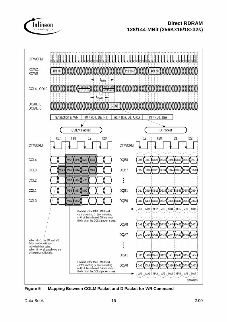
COLM Packet to D Packet Mapping
Figure 5 shows a write operation initiated by a WR command in a COLC packet. If a subset of the16 bytes of write data are to be written, then a COLM packet is transmitted on the COL pins a timetRTR after the COLC packet containing the WR command. The M bit of the COLM packet is set toindicate that it contains the MA and MB mask fields. Note that this COLM packet is aligned with theCOLC packet which causes the write buffer to be retired. See Figure 17 for more details.
If all 16 bytes of the D data packet are to be written, then no further control information is required.The packet slot that would have been used by the COLM packet (tRTR after the COLC packet) isavailable to be used as an COLX packet. This could be used for a PREX precharge command or fora housekeeping command (this case is not shown). The M bit is not asserted in an COLX packetand causes all 16 bytes of the previous WR to be written unconditionally. Note that a RD commandwill never need a COLM packet, and will always be able to use the COLX packet option (a readoperation has no need for the byte-write-enable control bits).
Figure 5 also shows the mapping between the MA and MB fields of the COLM packet and bytes ofthe D packet on the DQA and DQB pins. Each mask bit controls whether a byte of data is written(= 1) or not written (= 0).
Direct RDRAM128/144-MBit (256K×16/18×32s)
Data Book 16 2.00
Figure 5 Mapping Between COLM Packet and D Packet for WR Command
the M bit of the COLM packet is one.(= 0) of the indicated DB bits whencontrols writing (= 1) or no writingEach bit of the MB7...MB0 field
the M bit of the COLM packet is one.(= 0) of the indicated DA bits whencontrols writing (= 1) or no writingEach bit of the MA7...MA0 field
When M = 0, all data bytes are
When M = 1, the MA and MB
writing unconditionally.
individual data bytes.fields control writing of
COL0
COL1
COL2
COL3
MB5
MB6
MB2
MB3 MB0
MB7
M = 1 MA6
MB4 MB1
MA4 MA2
DA55DA46DA37DA28DA19DA10DA1 DA64DQA1
MA1
DA9DQA0 DA0
MA0 MA5
DA45
MA3
DA27DA18
MA2
DA36
MA4
SPA04209
MA7
DA63DA54
MA6
DB16
DB10
DB9
DA17
DA16
MB1MB0
DQA7 DA7
DQA8 DA8
MA0
DQB0
DQB1
DB0
DB1
DQB7 DB7
MB7MB2 MB5MB4MB3 MB6
DA53
DA52DA34DA25 DA44
DA35DA26 DA45
DA70DA61
DA71DA62
DB52
DB46
DB45
DB28
DB27DB18
DB19
DB36
DB37
DB34DB25 DB44
DB64
DB63DB54
DB55
DB70DB61
T12
T19
COLM Packet
a0 = Da, Ba, Ra
ACT a0
Transaction a: WR
T17
COL4
CTM/CFM
MA7 MA5 MA3
T18
DQA8...0DQB8...0
COL4...COL0
ROW0
WR a1
T2
CTM/CFM
ROW2...
T1T0 T7T3 T4 T5 T6 T8 T9 T10 T11
ACT b0PRER a2
DB17
a1 = Da, Ba, Ca1
MA1
T20
CTM/CFM
DQB8 DB8
T19
CWDt
D (a1)
RTRt
MSK (a1)retire (a1)
a3 = Da, Ba
DB53DB35DB26 DB45
D Packet
T20 T21
DB71DB62
T22
T17T14T13 T15 T16 T19T18 T20 T21 T24T23T22 T25 T26 T29T28T27 T30 T31 T34T33T32 T35 T36 T39T37 T38 T40 T41 T46T44T42 T43 T45 T47
Data Book 17 2.00
Direct RDRAM128/144-MBit (256K×16/18×32s)
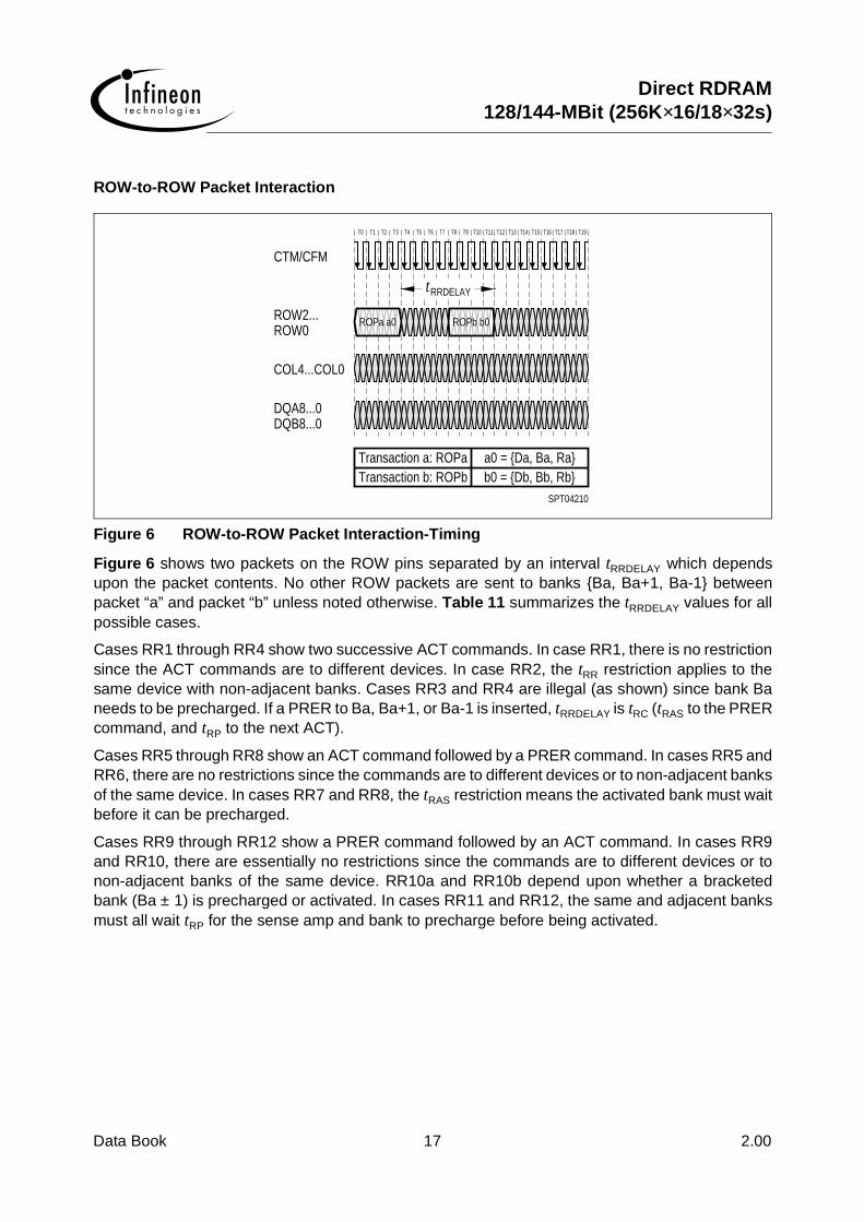
ROW-to-ROW Packet Interaction
Figure 6 ROW-to-ROW Packet Interaction-Timing
Figure 6 shows two packets on the ROW pins separated by an interval tRRDELAY which dependsupon the packet contents. No other ROW packets are sent to banks Ba, Ba+1, Ba-1 betweenpacket “a” and packet “b” unless noted otherwise. Table 11 summarizes the tRRDELAY values for allpossible cases.
Cases RR1 through RR4 show two successive ACT commands. In case RR1, there is no restrictionsince the ACT commands are to different devices. In case RR2, the tRR restriction applies to thesame device with non-adjacent banks. Cases RR3 and RR4 are illegal (as shown) since bank Baneeds to be precharged. If a PRER to Ba, Ba+1, or Ba-1 is inserted, tRRDELAY is tRC (tRAS to the PRERcommand, and tRP to the next ACT).
Cases RR5 through RR8 show an ACT command followed by a PRER command. In cases RR5 andRR6, there are no restrictions since the commands are to different devices or to non-adjacent banksof the same device. In cases RR7 and RR8, the tRAS restriction means the activated bank must waitbefore it can be precharged.
Cases RR9 through RR12 show a PRER command followed by an ACT command. In cases RR9and RR10, there are essentially no restrictions since the commands are to different devices or tonon-adjacent banks of the same device. RR10a and RR10b depend upon whether a bracketedbank (Ba ± 1) is precharged or activated. In cases RR11 and RR12, the same and adjacent banksmust all wait tRP for the sense amp and bank to precharge before being activated.
Transaction b: ROPbTransaction a: ROPa
DQB8...0DQA8...0
b0 = Db, Bb, Rba0 = Da, Ba, Ra
SPT04210
COL4...COL0
ROW2...
CTM/CFM
ROPa a0
T0 T1 T3T2 T4 T17T11
ROPb b0
T8
RRDELAYt
T5 T6 T7 T9 T10 T14T12 T13 T15 T16 T18 T19
ROW0

Direct RDRAM128/144-MBit (256K×16/18×32s)
Data Book 18 2.00
ROW-to-ROW Interaction (cont’d)
Cases RR13 through RR16 summarize the combinations of two successive PRER commands. Incase RR13 there is no restriction since two devices are addressed. In RR14, tPP applies, since thesame device is addressed. In RR15 and RR16, the same bank or an adjacent bank may be givenrepeated PRER commands with only the tPP restriction.
Two adjacent banks can’t be activate simultaneously. A precharge command to one bank will thusaffect the state of the adjacent banks (and sense amps). If bank Ba is activate and a PRER isdirected to Ba, then bank Ba will be precharged along with sense amps Ba-1/Ba and Ba/Ba+1. Ifbank Ba+1 is activate and a PRER is directed to Ba, then bank Ba+1 will be precharged along withsense amps Ba/Ba+1 and Ba+1/Ba+2. If bank Ba-1 is activate and a PRER is directed to Ba, thenbank Ba-1 will be precharged along with sense amps Ba/Ba-1 and Ba-1/Ba-2.
A ROW packet may contain commands other than ACT or PRER. The REFA and REFP commandsare equivalent to ACT and PRER for interaction analysis purposes. The interaction rules of theNAPR, NAPRC, PDNR, RLXR, ATTN, TCAL, and TCEN commands are discussed in later sections(see Table 8 for cross-ref).
Table 11 ROW-to-ROW Packet Interaction - Rules
Case # ROPa Da Ba Ra ROPb Db Bb Rb tRRDELAY Example
RR1 ACT Da Ba Ra ACT /= Da xxxx x…x tPACKET Figure 11
RR2 ACT Da Ba Ra ACT == Da /= Ba, Ba+1, Ba-1 x…x tRR Figure 11
RR3 ACT Da Ba Ra ACT == Da == Ba+1, Ba-1 x…x tRC - illegal unless PRER to Ba/Ba+1/Ba-1
Figure 10
RR4 ACT Da Ba Ra ACT == Da == Ba x…x tRC - illegal unless PRER to Ba/Ba+1/Ba-1
Figure 10
RR5 ACT Da Ba Ra PRER /= Da xxxx x…x tPACKET Figure 11
RR6 ACT Da Ba Ra PRER == Da /= Ba, Ba+1, Ba-1 x…x tPACKET Figure 11
RR7 ACT Da Ba Ra PRER == Da == Ba+1, Ba-1 x…x tRAS Figure 10
RR8 ACT Da Ba Ra PRER == Da == Ba x…x tRAS Figure 15
RR9 PRER Da Ba Ra ACT /= Da xxxx x…x tPACKET Figure 12
RR10 PRER Da Ba Ra ACT == Da /= Ba, Ba±1, Ba±2
x…x tPACKET Figure 12
RR10a PRER Da Ba Ra ACT == Da == Ba+2 x…x tPACKET/tRP if Ba+1 is precharged/activated.
–
RR10b PRER Da Ba Ra ACT == Da == Ba-2 x…x tPACKET/tRP if Ba-1 is precharged/activated.
–
RR11 PRER Da Ba Ra ACT == Da == Ba+1, Ba-1 x…x tRP Figure 10
RR12 PRER Da Ba Ra ACT == Da == Ba x…x tRP Figure 10
RR13 PRER Da Ba Ra PRER /= Da xxxx x…x tPACKET Figure 12
RR14 PRER Da Ba Ra PRER == Da /= Ba, Ba+1, Ba-1 x…x tPP Figure 12
RR15 PRER Da Ba Ra PRER == Da == Ba+1, Ba-1 x…x tPP Figure 12
RR16 PRER Da Ba Ra PRER == Da == Ba x…x tPP Figure 12

Data Book 19 2.00
Direct RDRAM128/144-MBit (256K×16/18×32s)
ROW-to-COL Packet Interaction
Figure 7 shows two packets on the ROW and COL pins. They must be separated by an intervaltRCDELAY which depends upon the packet contents. Table 12 summarizes the tRCDELAY values for allpossible cases. Note that if the COL packet is earlier than the ROW packet, it is considered aCOL-to-ROW packet interaction.
Cases RC1 through RC5 summarize the rules when the ROW packet has an ACT command.Figure 15 and Figure 16 show examples of RC5 - an activation followed by a read or write. RC4 isan illegal situation, since a read or write of a precharged banks is being attempted (remember thatfor a bank to be activated, adjacent banks must be precharged). In cases RC1, RC2, and RC3,there is no interaction of the ROW and COL packets.
Figure 7 ROW-to-COL Packet Interaction - Timing
Cases RC6 through RC8 summarize the rules when the ROW packet has a PRER command. Thereis either no interaction (RC6 through RC9) or an illegal situation with a read or write of a prechargedbank (RC9).
The COL pins can also schedule a precharge operation with a RDA, WRA, or PREC command ina COLC packet or a PREX command in a COLX packet. The constraints of these prechargeoperations may be converted to equivalent PRER command constraints using the rulessummarized in Figure 14.
Transaction b: COPbTransaction a: ROPa
DQB8...0DQA8...0
b1 = Db, Bb, Cb1a0 = Da, Ba, Ra
SPT04211
COL4...COL0
ROW2...
CTM/CFM
COPb b1
T0 T1 T3T2 T4 T17T11
ROPa a0
T8
RCDELAYt
T5 T6 T7 T9 T10 T14T12 T13 T15 T16 T18 T19
ROW0

Direct RDRAM128/144-MBit (256K×16/18×32s)
Data Book 20 2.00
COL-to-COL Packet Interaction
Figure 8 COL-to-COL Packet Interaction-Timing
Figure 8 shows three arbitrary packets on the COL pins. Packets “b” and “c” must be separated byan interval tCCDELAY which depends upon the command and address values in all three packets.Table 13 summarizes the tCCDELAY values for all possible cases.
Cases CC1 through CC5 summarize the rules for every situation other than the case when COPbis a WR command and COPc is a RD command. In CC3, when a RD command is followed by a WRcommand, a gap of tCAC – tCWD must be inserted between the two COL packets. See Figure 4 formore explanation of why this gap is needed. For cases CC1, CC2, CC4, and CC5, there is norestriction (tCCDELAY is tCC).
Table 12 ROW-to-COL Packet Interaction - Rules
Case # ROPa Da Ba Ra COPb Db Bb Cb1 tRCDELAY Example
RC1 ACT Da Ba Ra NOCOP, RD, retire /= Da xxxx x…x 0 –
RC2 ACT Da Ba Ra NOCOP == Da xxxx x…x 0 –
RC3 ACT Da Ba Ra RD, retire == Da /= Ba, Ba+1, Ba-1 x…x 0 –
RC4 ACT Da Ba Ra RD, retire == Da == Ba+1, Ba-1 x…x Illegal –
RC5 ACT Da Ba Ra RD, retire == Da == Ba x…x tRCD Figure 15
RC6 PRER Da Ba Ra NOCOP, RD, retire /= Da xxxx x…x 0 –
RC7 PRER Da Ba Ra NOCOP == Da xxxx x…x 0 –
RC8 PRER Da Ba Ra RD, retire == Da /= Ba, Ba+1, Ba-1 x…x 0 –
RC9 PRER Da Ba Ra RD, retire == Da == Ba+1, Ba-1 x…x Illegal –
Transaction b: COPbTransaction a: COPa
DQB8...0DQA8...0
b1 = Db, Bb, Cb1a1 = Da, Ba, Ca1
SPT04212
COL4...COL0
ROW2...
CTM/CFM
T0 T1 T3T2 T4 T17T11T8
CCDELAYt
T5 T6 T7 T9 T10 T14T12 T13 T15 T16 T18 T19
ROW0
Transaction c: COPc c1 = Dc, Bc, Cc1
COPa a1 COPb b1 COPc c1

Data Book 21 2.00
Direct RDRAM128/144-MBit (256K×16/18×32s)
In cases CC6 through CC10, COPb is a WR command and COPc is a RD command. The tCCDELAY
value needed between these two packets depends upon the command and address in the packetwith COPa. In particular, in case CC6 when there is WR-WR-RD command sequence directed tothe same device, a gap will be needed between the packets with COPb and COPc. The gap willneed a COLC packet with a NOCOP command directed to any device in order to force an automaticretire to take place. Figure 18 (right) provides a more detailed explanation of this case.
In case CC10, there is a RD-WR-RD sequence directed to the same device. If a prior write to thesame device is unretired when COPa is issued, then a gap will be needed between the packets withCOPb and COPc as in case CC6. The gap will need a COLC packet with a NOCOP commanddirected to any device in order to force an automatic retire to take place.
Cases CC7, CC8, and CC9 have no restriction (tCCDELAY is tCC).
For the purposes of analyzing COL-to-ROW interactions, the PREC, WRA, and RDA commands ofthe COLC packet are equivalent to the NOCOP, WR, and RD commands. These commands alsocause a precharge operation PREC to take place. This precharge may be converted to anequivalent PRER command on the ROW pins using the rules summarized in Figure 14.
Table 13 COL-to-COL Packet Interaction - Rules
Case # COPa Da Ba Ca1 COPb Db Bb Cb1 COPc Dc Bc Cc1 tCCDELAY Example
CC1 xxxx xxxxx x…x x…x NOCOP Db Bb Cb1 xxxx xxxxx x…x x…x tCC –
CC2 xxxx xxxxx x…x x…x RD,WR Db Bb Cb1 NOCOP xxxxx x…x x…x tCC –
CC3 xxxx xxxxx x…x x…x RD Db Bb Cb1 WR xxxxx x…x x…x tCC+tCAC-tCWD Figure 4
CC4 xxxx xxxxx x…x x…x RD Db Bb Cb1 RD xxxxx x…x x…x tCC Figure 15
CC5 xxxx xxxxx x…x x…x WR Db Bb Cb1 WR xxxxx x…x x…x tCC Figure 16
CC6 WR == Db x x…x WR Db Bb Cb1 RD == Db x…x x…x tRTR Figure 18
CC7 WR == Db x x…x WR Db Bb Cb1 RD /= Db x…x x…x tCC –
CC8 WR /= Db x x…x WR Db Bb Cb1 RD == Db x…x x…x tCC –
CC9 NOCOP == Db x x…x WR Db Bb Cb1 RD == Db x…x x…x tCC –
CC10 RD == Db x x…x WR Db Bb Cb1 RD == Db x…x x…x tCC –

Direct RDRAM128/144-MBit (256K×16/18×32s)
Data Book 22 2.00
COL-to-ROW Packet Interaction
Figure 9 COL-to-ROW Packet Interaction - Timing
Figure 9 shows arbitrary packets on the COL and ROW pins. They must be separated by aninterval tCRDELAY which depends upon the command and address values in the packets. Table 14summarizes the tCRDELAY value for all possible cases.
Cases CR1, CR2, CR3, and CR9 show no interaction between the COL and ROW packets, eitherbecause one of the commands is a NOP or because the packets are directed to different devices orto non-adjacent banks.
Case CR4 is illegal because an already-activated bank is to be re-activated without beingprecharged Case CR5 is illegal because an adjacent bank can’t be activated or precharged untilbank Ba is precharged first.
In case CR6, the COLC packet contains a RD command, and the ROW packet contains a PRERcommand for the same bank. The tRDP parameter specifies the required spacing.
Likewise, in case CR7, the COLC packet causes an automatic retire to take place, and the ROWpacket contains a PRER command for the same bank. The tRTP parameter specifies the requiredspacing.
Case CR8 is labeled “Hazardous” because a WR command should always be followed by anautomatic retire before a precharge is scheduled. Figure 19 shows an example of what can happenwhen the retire is not able to happen before the precharge.
For the purposes of analyzing COL-to-ROW interactions, the PREC, WRA, and RDA commands ofthe COLC packet are equivalent to the NOCOP, WR, and RD commands. These commands alsocause a precharge operation to take place. This precharge may converted to an equivalent PRERcommand on the ROW pins using the rules summarized in Figure 14.
A ROW packet may contain commands other than ACT or PRER. The REFA and REFP commandsare equivalent to ACT and PRER for interaction analysis purposes. The interaction rules of theNAPR, PDNR, and RLXR commands are discussed in a later section.
Transaction b: ROPbTransaction a: COPa
DQB8...0DQA8...0
b0 = Db, Bb, Rba1 = Da, Ba, Ca1
SPT04213
COL4...COL0
ROW2...
CTM/CFM
COPa a1
T0 T1 T3T2 T4 T17T11
ROPb b0
T8
CRDELAYt
T5 T6 T7 T9 T10 T14T12 T13 T15 T16 T18 T19
ROW0

Data Book 23 2.00
Direct RDRAM128/144-MBit (256K×16/18×32s)
Table 14 COL-to-ROW Packet Interaction - Rules
Case # COPa Da Ba Ca1 ROPb Db Bb Rb tCRDELAY Example
CR1 NOCOP Da Ba Ca1 x…x xxxxx xxxx x…x 0 –
CR2 RD/WR Da Ba Ca1 x…x /= Da xxxx x…x 0 –
CR3 RD/WR Da Ba Ca1 x…x == Da /= Ba, Ba+1, Ba-1 x…x 0 –
CR4 RD/WR Da Ba Ca1 ACT == Da == Ba x…x Illegal –
CR5 RD/WR Da Ba Ca1 ACT == Da == Ba+1, Ba-1 x…x Illegal –
CR6 RD Da Ba Ca1 PRER == Da == Ba, Ba+1, Ba-1 x…x tRDP Figure 15
CR7 retire1) Da Ba Ca1 PRER == Da == Ba, Ba+1, Ba-1 x…x tRTP Figure 16
CR8 WR2) Da Ba Ca1 PRER == Da == Ba, Ba+1, Ba-1 x…x 0 Figure 19
CR9 xxxx Da Ba Ca1 NOROP xxxxx xxxx x…x 0 –
1) This is any command which permits the write buffer of device Da to retire (see Table 9). “Ba” is the bank address in the writebuffer.
2) This situation is hazardous because the write buffer will be left unretired while the targeted bank is precharged. See Figure 19.

Direct RDRAM128/144-MBit (256K×16/18×32s)
Data Book 24 2.00
ROW-to-ROW Examples
Figure 10 shows examples of some of the ROW-to-ROW packet spacings from Table 11. Acomplete sequence of activate and precharge commands is directed to a bank. The RR8 and RR12rules apply to this sequence. In addition to satisfying the tRAS and tRP timing parameters, theseparation between ACT commands to the same bank must also satisfy the tRC timing parameter(RR4).
When a bank is activated, it is necessary for adjacent banks to remain precharged. As a result, theadjacent banks will also satisfy parallel timing constraints; in the example, the RR11 and RR3 rulesare analogous to the RR12 and RR4 rules.
Figure 10 Row Packet Example
Figure 11 shows examples of the ACT-to-ACT (RR1, RR2) and ACT-to-PRER (RR5, RR6)command spacings from Table 11. In general, the commands in ROW packets may be spaced aninterval tPACKET apart unless they are directed to the same or adjacent banks or unless they are asimilar command type (both PRER or both ACT) directed to the same device.
DQA8...0DQB8...0
COL4...COL0
tRC
SPA04214
T24
Same Device
Same Device
Same DeviceSame Device
Same Device
ROW0
CTM/CFM
ROW2... ACT a0
T2T0 T1 T3 T4 T14T7T5 T6 T8 T9 T10 T11 T13T12
RASt
T19T15 T16 T18T17 T20 T21 T23T22
a0 = Da, Ba, Raa1 = Da, Ba+1
b0 = Da, Ba+1, Rb
b0 = Da, Ba, Rbb0 = Da, Ba+1, Rb
b0 = Da, Ba, RbRR11Adjacent Bank
T34
RR12
ACT b0PRER a1
RPt
T29
Same Bank
T25 T26 T27 T28 T30 T31 T32 T33 T39T36T35 T37 T38 T41T40 T42 T43
RR7
RR4RR3
Adjacent BankAdjacent Bank
Same Bank
T46T45T44 T47

Data Book 25 2.00
Direct RDRAM128/144-MBit (256K×16/18×32s)
Figure 11 Row Packet Example
Figure 12 shows examples of the PRER-to-PRER (RR13, RR14) and PRER-to-ACT (RR9, RR10)command spacings from Table 12. The RR15 and RR16 cases (PRER-to-PRER to same oradjacent banks) are not shown, but are similar to RR14. In general, the commands in ROW packetsmay be spaced an interval tPACKET apart unless they are directed to the same or adjacent banks orunless they are a similar command type (both PRER or both ACT) directed to the same device.
DQA8...0DQB8...0
COL4...COL0
SPA04215
T24
Different DeviceSame Device
Same Device
Different Device
ACT b0ROW0
CTM/CFM
ROW2... ACT a0
PACKETt
T2T0 T1 T3 T4 T14
ACT a0
T7T5 T6 T8 T11 T13T12
t
ACT c0
RR
T19T15 T16 T18T17 T20 T21 T23T22
a0 = Da, Ba, Rab0 = Db, Bb, Rb
c0 = Da, Bc, Rcb0 = Db, Bb, Rbc0 = Da, Bc, Rc
Any Bank
T34
Non-adjacent Bank
PRER b0
PACKET
ACT a0
t
T29T27 T28 T30 T31 T32 T33
ACT a0
PACKETt
T39T36T35
RR6
T41T40 T42 T43
Non-adjacent BankAny Bank RR1
RR5RR2
PRER c0
T46T45T44 T47

Direct RDRAM128/144-MBit (256K×16/18×32s)
Data Book 26 2.00
Figure 12 Row Packet Examples
Row and Column Cycle Description
Activate: A row cycle begins with the activate (ACT) operation. The activation process isdestructive; the act of sensing the value of a bit in a bank’s storage cell transfers the bit to the senseamp, but leaves the original bit in the storage cell with an incorrect value.
Restore: Because the activation process is destructive, a hidden operation called restore isautomatically performed. The restore operation rewrites the bits in the sense amp back into thestorage cells of the activated row of the bank.
Read/Write: While the restore operation takes place, the sense amp may be read (RD) and written(WR) using column operations. If new data is written into the sense amp, it is automaticallyforwarded to the storage cells of the bank so the data in the activated row and the data in the senseamp remain identical.
Precharge: When both the restore operation and the column operations are completed, the senseamp and bank are precharged (PRE). This leaves them in the proper state to begin another activateoperation.
Intervals: The activate operation requires the interval tRCD,MIN to complete. The hidden restoreoperation requires the interval tRAS,MIN – tRCD,MIN to complete. Column read and write operations arealso performed during the tRAS,MIN – tRCD,MIN interval (if more than about four column operations are
COL4...COL0
DQB8...0DQA8...0
SPA04216
T24
Same Device
Same Device
Same DeviceDifferent Device
Same DeviceDifferent Device
PRER b0ROW2...
CTM/CFM
ROW0PRER a0
PACKETt
T2T0 T1 T3 T4 T14
PRER a0
T7T5 T6 T8 T11 T13T12
t
PRER c0
PP
T19T15 T16 T18T17 T20 T21 T23T22
c0 = Da, Ba+1, Rcb0 = Db, Bb, Rbc0 = Da, Bc, Rc
c0 = Da, Ba, Rcc0 = Da, Bc, Rcb0 = Db, Bb, Rba0 = Da, Ba, Ra
Any Bank
T34
Non-adjacent Bank
ACT b0PRER a0
PACKETt
T29T27 T28 T30 T31 T32 T33
PRER a0
PACKETt
T39T36T35
RR10
T41T40 T42 T43
Non-adjacent BankAny Bank
Same BankAdjacent Bank
RR13
RR15RR16RR9
RR14
ACT c0
T46T45T44 T47

Data Book 27 2.00
Direct RDRAM128/144-MBit (256K×16/18×32s)
performed, this interval must be increased). The precharge operation requires the interval tRP,MIN tocomplete.
Adjacent Banks: An RDRAM with a “s” designation (256K × 32s × 16/18) indicates it contains “splitbanks”. This means the sense amps are shared between two adjacent banks. The only exceptionis that sense amp 0, 15, 30, and 31 are not shared. When a row in a bank is activated, the twoadjacent sense amps are connected to (associated with) that bank and are not available for use bythe two adjacent banks. These two adjacent banks must remain precharged while the selected bankgoes through its activate, restore, read/write, and precharge operations.
For example (referring to the block diagram of Figure 2), if bank 5 is accessed, sense amp 4/5 andsense amp 5/6 will both be loaded with one of the 512 rows (with 512 bytes loaded into each senseamp from the 1 Kbyte row - 256 bytes to the DQA side and 256 bytes to the DQB side). While thisrow from bank 5 is being accessed, no rows may be accessed in banks 4 or 6 because of the senseamp sharing.
Precharge Mechanisms
Figure 13 shows an example of precharge with the ROWR packet mechanism. The PRERcommand must occur a time tRAS after the ACT command, and a time tRP before the next ACTcommand. This timing will serve as a baseline against which the other precharge mechanisms canbe compared.
Figure 13 Precharge via PRER Command in ROWR Packet
Figure 14 (top) shows an example of precharge with a RDA command. A bank is activated with anROWA packet on the ROW pins. Then, a series of four dualocts are read with RD commands inCOLC packets on the COL pins. The fourth of these commands is a RDA, which causes the bankto automatically precharge when the final read has finished. The timing of this automatic prechargeis equivalent to a PRER command in an ROWR packet on the ROW pins that is offset a time tOFFP
SPA04217
T24
ROW2...
COL4...COL0
DQB8...0DQA8...0
RPt
CTM/CFM
T2T1T0 T3 T4 T14T7T5 T6 T8 T9 T12T10 T11 T13 T19T17T15 T16 T18 T20 T21 T23T22 T44T34T29T25 T26 T28T27 T30 T31 T33T32 T39T35 T36 T37 T38 T40 T41 T42 T43 T46T45 T47
ACT a0 ACT b0PRER a5ROW0
RASt
tRC
a0 = Da, Ba, Raa5 = Da, Ba
b0 = Da, Ba, Rb

Direct RDRAM128/144-MBit (256K×16/18×32s)
Data Book 28 2.00
from the COLC packet with the RDA command. The RDA command should be treated as a RDcommand in a COLC packet as well as a simultaneous (but offset) PRER command in an ROWRpacket when analyzing interactions with other packets.
Figure 14 (middle) shows an example of precharge with a WRA command. As in the RDA example,a bank is activated with an ROWA packet on the ROW pins. Then, two dualocts are written with WRcommands in COLC packets on the COL pins. The second of these commands is a WRA, whichcauses the bank to automatically precharge when the final write has been retired. The timing of thisautomatic precharge is equivalent to a PRER command in an ROWR packet on the ROW pins thatis offset a time tOFFP from the COLC packet that causes the automatic retire. The WRA commandshould be treated as a WR command in a COLC packet as well as a simultaneous (but offset) PRERcommand in an ROWR packet when analyzing interactions with other packets. Note that theautomatic retire is triggered by a COLC packet a time tRTR after the COLC packet with the WRcommand unless the second COLC contains a RD command to the same device. This is describedin more detail in Figure 17.
Figure 14 (bottom) shows an example of precharge with a PREX command in an COLX packet. Abank is activated with an ROWA packet on the ROW pins. Then, a series of four dualocts are readwith RD commands in COLC packets on the COL pins. The fourth of these COLC packets includesan COLX packet with a PREX command. This causes the bank to precharge with timing equivalentto a PRER command in an ROWR packet on the ROW pins that is offset a time tOFFP from the COLXpacket with the PREX command.

Data Book 29 2.00
Direct RDRAM128/144-MBit (256K×16/18×32s)
Figure 14 Offsets for Alternate Precharge Mechanisms
D (a2)
a1 = Da, Ba, Ca1
retire (a2)MSK (a2)
T24
PREX a5
a1 = Da, Ba, Ca1a3 = Da, Ba, Ca3
Transaction a: RD
DQB8...0DQA8...0
a0 = Da, Ba, Ra
Q (a1)
Transaction a: WR
COLC Packet: PREX Precharge Offset
The PREX precharge is equivalent to a PRER command here
CTM/CFM
ROW0
COL4...COL0
ROW2... ACT a0
T2T0 T1 T3 T4
COL4...COL0
DQB8...0DQA8...0
T14
RD a2RD a1
T7T5 T6 T8 T9 T10 T11 T13T12
RD a3 RD a4
T19T15 T16 T18T17 T20 T21 T23T22
a0 = Da, Ba, Ra
D (a1)
retire (a1)MSK (a1)
RTRt
a5 = Da, Ba
Q (a4)
a2 = Da, Ba, Ca2a4 = Da, Ba, Ca4
Q (a2) Q (a3)
SPA04218
a5 = Da, Ba
T34
ACT b0PRER a5
OFFPt
T29T25 T26 T27 T28 T30 T31 T32 T33 T39T36T35 T37 T38 T41T40 T42 T43
a2 = Da, Ba, Ca2
OFFPt
T46T45T44 T47
T24
T24
a1 = Da, Ba, Ca1a3 = Da, Ba, Ca3
The WRA precharge (triggered by the automatic retire) is equivalent to a PRER command here
Transaction a: RD
COLC Packet: WRA Precharge Offset
The RDA precharge is equivalent to a PRER command here
ROW2...ROW0
CTM/CFM
ACT a0
T2T0 T1 T3 T4
ROW2...ROW0
DQB8...0DQA8...0
COL4...COL0
ACT a0
T14
a0 = Da, Ba, Ra
T7T5 T6 T8 T9 T10 T11 T13T12 T19T15 T16 T18T17 T20 T21 T23T22
RD a2RD a1 RD a3 RD a4
Q (a1)
COLC Packet: RDA Precharge Offset
CTM/CFM
T2T0 T1 T3 T4 T14T7T5 T6 T8 T9 T10 T11 T13T12 T19T15 T16 T18T17 T20 T21 T23T22
a5 = Da, Ba
T34
ACT b0
a2 = Da, Ba, Ca2a4 = Da, Ba, Ca4
PRER a5
T29T25 T26 T27 T28 T30 T31 T32 T33 T39T36T35 T37 T38 T41T40 T42 T43
ACT b0
Q (a4)Q (a2) Q (a3)
PRER a5
OFFPt
T46T45T44 T47
T34T29T25 T26 T27 T28 T30 T31 T32 T33 T39T36T35 T37 T38 T41T40 T42 T43 T46T45T44 T47
WR a1 WRA a2

Direct RDRAM128/144-MBit (256K×16/18×32s)
Data Book 30 2.00
Read Transaction - Example
Figure 15 shows an example of a read transaction. It begins by activating a bank with an ACT a0command in an ROWA packet. A time tRCD later a RD a1 command is issued in a COLC packet.Note that the ACT command includes the device, bank, and row address (abbreviated as a0) whilethe RD command includes device, bank, and column address (abbreviated as a1). A time tCAC afterthe RD command the read data dualoct Q(a1) is returned by the device. Note that the packets onthe ROW and COL pins use the end of the packet as a timing reference point, while the packets onthe DQA/DQB pins use the beginning of the packet as a timing reference point.
A time tCC after the first COLC packet on the COL pins a second is issued. It contains a RD a2command. The a2 address has the same device and bank address as the a1 address (and a0address), but a different column address. A time tCAC after the second RD command a second readdata dualoct Q(a2) is returned by the device.
Next, a PRER a3 command is issued in an ROWR packet on the ROW pins. This causes the bankto precharge so that a different row may be activated in a subsequent transaction or so that anadjacent bank may be activated. The a3 address includes the same device and bank address as thea0, a1, and a2 addresses. The PRER command must occur a time tRAS or more after the originalACT command (the activation operation in any DRAM is destructive, and the contents of theselected row must be restored from the two associated sense amps of the bank during the tRAS
interval). The PRER command must also occur a time tRDP or more after the last RD command. Notethat the tRDP value shown is greater than the tRDP,MIN specification in Table 23. This transactionexample reads two dualocts, but there is actually enough time to read three dualocts before tRDP
becomes the limiting parameter rather than tRAS. If four dualocts were read, the packet with PRERwould need to shift right (be delayed) by one tCYCLE (note - this case is not shown).
Finally, an ACT b0 command is issued in an ROWR packet on the ROW pins. The second ACTcommand must occur a time tRC or more after the first ACT command and a time tRP or more afterthe PRER command. This ensures that the bank and its associated sense amps are precharged.This example assumes that the second transaction has the same device and bank address as thefirst transaction, but a different row address. Transaction b may not be started until transaction a hasfinished. However, transactions to other banks or other devices may be issued during transaction a

Data Book 31 2.00
Direct RDRAM128/144-MBit (256K×16/18×32s)
Figure 15 Read Transaction Example
Write Transaction - Example
Figure 16 shows an example of a write transaction. It begins by activating a bank with an ACT a0command in an ROWA packet. A time tRCD – tRTR later a WR a1 command is issued in a COLCpacket (note that the tRCD interval is measured to the end of the COLC packet with the first retirecommand). Note that the ACT command includes the device, bank, and row address (abbreviatedas a0) while the WR command includes device, bank, and column address (abbreviated as a1). Atime tCWD after the WR command the write data dualoct D(a1) is issued. Note that the packets on theROW and COL pins use the end of the packet as a timing reference point, while the packets on theDQA/DQB pins use the beginning of the packet as a timing reference point.
A time tCC after the first COLC packet on the COL pins a second COLC packet is issued. It containsa WR a2 command. The a2 address has the same device and bank address as the a1 address (anda0 address), but a different column address. A time tCWD after the second WR command a secondwrite data dualoct D(a2) is issued.
A time tRTR after each WR command an optional COLM packet MSK (a1) is issued, and at the sametime a COLC packet is issued causing the write buffer to automatically retire. See Figure 17 formore detail on the write/retire mechanism. If a COLM packet is not used, all data bytes areunconditionally written. If the COLC packet which causes the write buffer to retire is delayed, thenthe COLM packet (if used) must also be delayed.
Next, a PRER a3 command is issued in an ROWR packet on the ROW pins. This causes the bankto precharge so that a different row may be activated in a subsequent transaction or so that anadjacent bank may be activated. The a3 address includes the same device and bank address as thea0, a1, and a2 addresses. The PRER command must occur a time tRAS or more after the original
a1 = Da, Ba, Ca1Transaction b: XXTransaction a: RD
DQA8...0DQB8...0
t
b0 = Da, Ba, Rba0 = Da, Ba, Ra
RCDttCAC
CC
Q (a1)
tCACt
RDP
a3 = Da, Baa2 = Da, Ba, Ca2
Q (a2)
SPT04219
T24
ROW2...
CTM/CFM
ROW0
COL4...COL0
ACT a0
T2T0 T1 T3 T4
RD a2RD a1
RASt
tRC
T14T7T5 T6 T8 T9 T10 T11 T13T12 T19T15 T16 T18T17 T20 T21 T23T22
ACT b0PRER a3
T34T29T25 T26 T27 T28 T30 T31 T32 T33 T39T36T35 T37 T38 T41T40 T42 T43 T46T45T44 T47

Direct RDRAM128/144-MBit (256K×16/18×32s)
Data Book 32 2.00
ACT command (the activation operation in any DRAM is destructive, and the contents of theselected row must be restored from the two associated sense amps of the bank during the tRAS
interval).
A PRER a3 command is issued in an ROWR packet on the ROW pins. The PRER command mustoccur a time tRTP or more after the last COLC which causes an automatic retire.
Finally, an ACT b0 command is issued in an ROWR packet on the ROW pins. The second ACTcommand must occur a time tRC or more after the first ACT command and a time tRP or more afterthe PRER command. This ensures that the bank and its associated sense amps are precharged.This example assumes that the second transaction has the same device and bank address as thefirst transaction, but a different row address. Transaction b may not be started until transaction a hasfinished. However, transactions to other banks or other devices may be issued during transaction a.
Figure 16 Write Transaction Example
D (a2)
MSK (a2)retire (a2)
a1 = Da, Ba, Ca1Transaction a: WRTransaction b: XX
DQB8...0DQA8...0
COL4...COL0
t
WR a2
a0 = Da, Ba, Rab0 = Da, Ba, Rb
WR a1
D (a1)
CWD
retire (a1)MSK (a1)
ttCWD
CC
a3 = Da, Baa2 = Da, Ba, Ca2
SPT04220
T24
CTM/CFM
ROW2...ROW0
ACT a0
T2T0 T1 T3 T4
RCDttRTR
tRTR
tRASt
RC
T14T7T5 T6 T8 T9 T10 T11 T13T12 T19T15 T16 T18T17 T20 T21 T23T22
ACT b0PRER a3
RTPt
RPt
T34T29T25 T26 T27 T28 T30 T31 T32 T33 T39T36T35 T37 T38 T41T40 T42 T43 T46T45T44 T47

Data Book 33 2.00
Direct RDRAM128/144-MBit (256K×16/18×32s)
Write/Retire - Examples
The process of writing a dualoct into a sense amp of an RDRAM bank occurs in two steps. The firststep consists of transporting the write command, write address, and write data into the write buffer.The second step happens when the RDRAM automatically retires the write buffer (with an optionalbytemask) into the sense amp. This two-step write process reduces the natural turn-around delaydue to the internal bidirectional data pins.
Figure 17 (left) shows an example of this two step process. The first COLC packet contains the WRcommand and an address specifying device, bank and column. The write data dualoct follows atime tCWD later. This information is loaded into the write buffer of the specified device. The COLCpacket which follows a time tRTR later will retire the write buffer. The retire will happen automaticallyunless (1) a COLC packet is not framed (no COLC packet is present and the S bit is zero), or (2) theCOLC packet contains a RD command to the same device. If the retire does not take place at timetRTR after the original WR command, then the device continues to frame COLC packets, looking forthe first that is not a RD directed to itself. A bytemask MSK(a1) may be supplied in a COLM packetaligned with the COLC that retires the write buffer at time tRTR after the WR command.
The memory controller must be aware of this two-step write/retire process. Controller performancecan be improved, but only if the controller design accounts for several side effects.
Figure 17 Normal Retire (left) and Retire/Read Ordering (right)
Figure 17 (right) shows the first of these side effects. The first COLC packet has a WR commandwhich loads the address and data into the write buffer. The third COLC causes an automatic retireof the write buffer to the sense amp. The second and fourth COLC packets (which bracket the retirepacket) contain RD commands with the same device, bank and column address as the original WRcommand. In other words, the same dualoct address that is written is read both before and after itis actually retired. The first RD returns the old dualoct value from the sense amp before it isoverwritten. The second RD returns the new dualoct value that was just written.
Transaction b: RDTransaction c: RD
Transaction a: WR
DQA8...0DQB8...0
Transaction a: WR a1 = Da, Ba, Ca1
CWDttRTR
D (a1) DQA8...0DQB8...0
D (a1)
c1 = Da, Ba, Ca1b1 = Da, Ba, Ca1a1 = Da, Ba, Ca1
CWDtRTRt
Q (b1)
SPT04221
Q (
WR a1
This RD gets the old dataRetire is automatic here unless:(1) No COLC packet (S = 0) or(2) COLC packet is RD to device Da
CTM/CFM
COL0COL4...
ROW0ROW2...
WR a1
T2T0 T1 T3 T4
retire (a1)MSK (a1) COL0
COL4...
ROW0ROW2...
CTM/CFM
T7T5 T6 T8 T9 T12T10 T11 T13 T14 T0 T1
This RD gets the new data
CAC
RD b1MSK (a1)retire (a1)
t
RD c1
CACt
T4T2 T3 T5 T6 T9T7 T8 T10 T11 T14T13T12 T15 T16 T19T18T17 T20 T21 T23T22
Direct RDRAM128/144-MBit (256K×16/18×32s)
Data Book 34 2.00
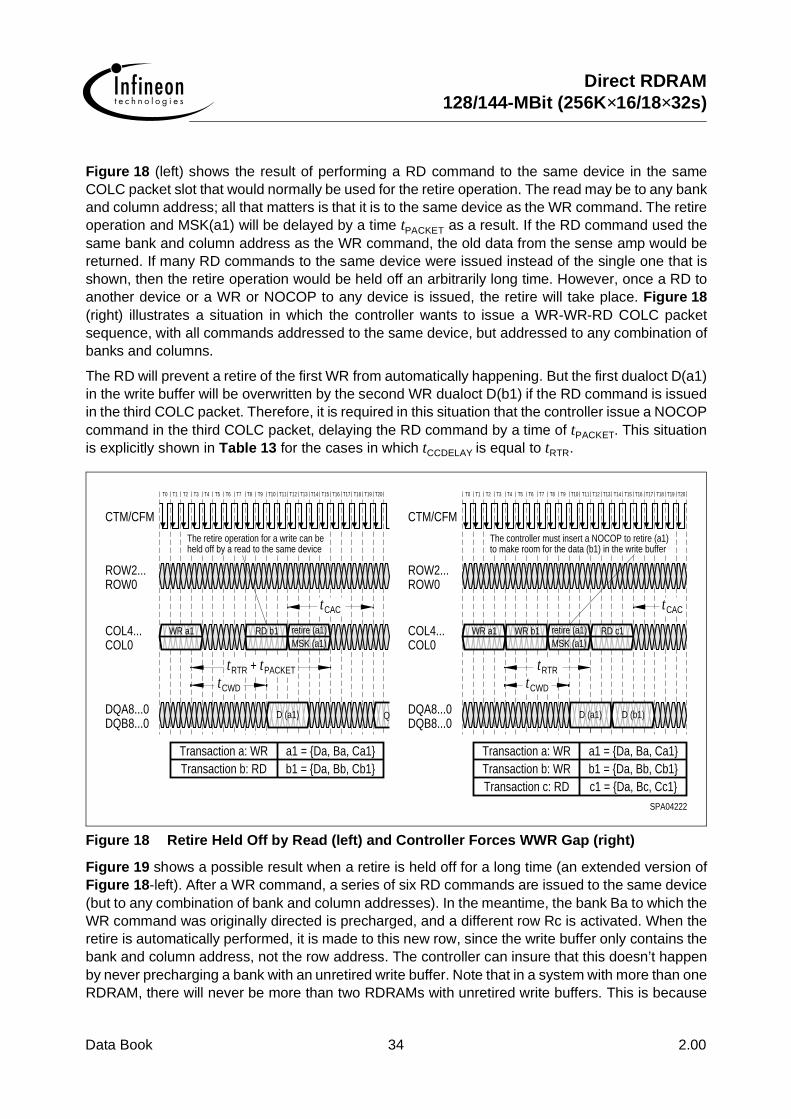
Figure 18 (left) shows the result of performing a RD command to the same device in the sameCOLC packet slot that would normally be used for the retire operation. The read may be to any bankand column address; all that matters is that it is to the same device as the WR command. The retireoperation and MSK(a1) will be delayed by a time tPACKET as a result. If the RD command used thesame bank and column address as the WR command, the old data from the sense amp would bereturned. If many RD commands to the same device were issued instead of the single one that isshown, then the retire operation would be held off an arbitrarily long time. However, once a RD toanother device or a WR or NOCOP to any device is issued, the retire will take place. Figure 18(right) illustrates a situation in which the controller wants to issue a WR-WR-RD COLC packetsequence, with all commands addressed to the same device, but addressed to any combination ofbanks and columns.
The RD will prevent a retire of the first WR from automatically happening. But the first dualoct D(a1)in the write buffer will be overwritten by the second WR dualoct D(b1) if the RD command is issuedin the third COLC packet. Therefore, it is required in this situation that the controller issue a NOCOPcommand in the third COLC packet, delaying the RD command by a time of tPACKET. This situationis explicitly shown in Table 13 for the cases in which tCCDELAY is equal to tRTR.
Figure 18 Retire Held Off by Read (left) and Controller Forces WWR Gap (right)
Figure 19 shows a possible result when a retire is held off for a long time (an extended version ofFigure 18-left). After a WR command, a series of six RD commands are issued to the same device(but to any combination of bank and column addresses). In the meantime, the bank Ba to which theWR command was originally directed is precharged, and a different row Rc is activated. When theretire is automatically performed, it is made to this new row, since the write buffer only contains thebank and column address, not the row address. The controller can insure that this doesn’t happenby never precharging a bank with an unretired write buffer. Note that in a system with more than oneRDRAM, there will never be more than two RDRAMs with unretired write buffers. This is because
DQB8...0DQA8...0
t
Transaction a: WRTransaction b: RD
DQA8...0DQB8...0
a1 = Da, Ba, Ca1b1 = Da, Bb, Cb1
PACKETRTR
CWD
t + t
D (a1) Q
c1 = Da, Bc, Cc1b1 = Da, Bb, Cb1a1 = Da, Ba, Ca1
tCWD
Transaction c: RDTransaction b: WRTransaction a: WR
t
D (a1)
RTR
D (b1)
SPA04222
ROW2...
CTM/CFM
COL4...
ROW0
COL0
T5
The retire operation for a write can beheld off by a read to the same device
CTM/CFM
COL0
ROW2...ROW0
COL4... WR a1
T0 T1 T2 T4T3
CAC
retire (a1)RD b1MSK (a1)
t
T15T10T6 T7 T9T8 T11 T12 T14T13 T20T16 T17 T19T18
The controller must insert a NOCOP to retire (a1)to make room for the data (b1) in the write buffer
WR a1 WR b1 retire (a1)MSK (a1)
RD c1
T0 T1 T3T2 T4 T5 T6 T9T8T7 T10 T11 T14T13T12 T15 T16
CACt
T19T18T17 T20

Data Book 35 2.00
Direct RDRAM128/144-MBit (256K×16/18×32s)
a WR command issued to one device automatically retires the write buffers of all other deviceswritten a time tRTR before or earlier.
Figure 19 Retire Held Off by Reads to Same Device, Write Buffer Retired to New Row
CWDt CACt
a0 = Da, Ba, Ra
b4 = Da, Bb, Cb4b1 = Da, Bb, Cb1
DQA8...0DQB8...0
Transaction a: WR
Transaction c: WR
Transaction b: RD
c0 = Da, Ba, Rcb5 = Da, Bb, Cb5b2 = Da, Bb, Cb2a1 = Da, Ba, Ca1
D (a1)
This sequence is hazardous
Q (b2)
b6 = Da, Bb, Cb6b3 = Da, Bb, Cb3
Q (b1)
a2 = Da, Ba
with cautionand must be used
WARNING
Q (b3) Q (b4)
SPT04223
Q (b5)
T24
ACT a0ROW2...ROW0
COL4...COL0
CTM/CFM
T2T0 T1 T3 T4
t
WR a1 RD b1 RD b2
RASt
RC
T14T7T5 T6 T8 T9 T10 T11 T13T12 T19T15 T16 T18T17 T20 T21 T23T22
MSK (a1)retire (a1)
write data in the new rowThe retire operation puts the
ACT c0
RD b5
RTR
tRCD
t
RD b3 RD b4
PRER a2
RPt
RD b6
T34T29T25 T26 T27 T28 T30 T31 T32 T33 T39T36T35 T37 T38 T41T40 T42 T43 T46T45T44 T47

Direct RDRAM128/144-MBit (256K×16/18×32s)
Data Book 36 2.00
Interleaved Write - Example
Figure 20 shows an example of an interleaved write transaction. Transactions similar to the onepresented in Figure 16 are directed to non-adjacent banks of a single RDRAM. This allows a newtransaction to be issued once every tRR interval rather than once every tRC interval (four times moreoften). The DQ data pin efficiency is 100% with this sequence.
With two dualocts of data written per transaction, the COL, DQA, and DQB pins are fully utilized.Banks are precharged using the WRA autoprecharge option rather than the PRER command in anROWR packet on the ROW pins.
In this example, the first transaction is directed to device Da and bank Ba. The next threetransactions are directed to the same device Da, but need to use different, non-adjacent banks Bb,Bc, Bd so there is no bank conflict. The fifth transaction could be redirected back to bank Ba withoutinterference, since the first transaction would have completed by then (tRC has elapsed). Eachtransaction may use any value of row address (Ra, Rb, …) and column address (Ca1, Ca2, Cb1,Cb2, …).
Figure 20 Interleaved Write Transaction with Two Dualoct Data Length
y1 = Da, Ba+4, Cy1z1 = Da, Ba+6, Cz1a1 = Da, Ba, Ca1
b1 = Da, Ba+2, Cb1c1 = Da, Ba+4, Cc1d1 = Da, Ba+6, Cd1
e1 = Da, Ba, Ce1f1 = Da, Ba+2, Cf1
Transaction y: WRTransaction z: WRTransaction a: WRTransaction b: WRTransaction c: WRTransaction d: WRTransaction e: WRTransaction f: WR
y0 = Da, Ba+4, Ryz0 = Da, Ba+6, Rza0 = Da, Ba, Ra
b0 = Da, Ba+2, Rbc0 = Da, Ba+4, Rcd0 = Da, Ba+6, Rd
e0 = Da, Ba, Ref0 = Da, Ba+2, Rf
SPA04224
f3 = Da, Ba+2e3 = Da, Ba
d3 = Da, Ba+6c3 = Da, Ba+4b3 = Da, Ba+2
z3 = Da, Ba+6y3 = Da, Ba+4
a3 = Da, Ba
f2 = Da, Ba+2, Cf2e2 = Da, Ba, Ce2
d2 = Da, Ba+6, Cd2c2 = Da, Ba+4, Cc2b2 = Da, Ba+2, Cb2
z2 = Da, Ba+6, Cz2y2 = Da, Ba+4, Cy2
a2 = Da, Ba, Ca2
T24
D (a1)
ACT a0ROW0ROW2...
COL4...COL0
DQB8...0DQA8...0 D (y1)
WR z1
CTM/CFM
T2T1T0 T3 T4
MSK (y2)
D (y2)
RCDt
WRA z2 WR a1
ACT b0
D (z2)D (z1)
tCWD
ACT c0
T7T6T5 T8 T9 T12T11T10 T13 T14 T17T15 T16 T18 T19
RCt
T22T20 T21 T23 T44
D (c2)
Transaction e can use thesame bank as transaction a
D (a2) D (b1)
ACT d0
tRR
D (c1)D (b2)
ACT e0 ACT f0
T34T29T27T25 T26 T28 T32T30 T31 T33 T39T37T35 T36 T38 T40 T41 T43T42 T45 T46 T47
D (x2) D (d1)
MSK (y1) MSK (z1)WR a2
MSK (z2)WR b1
MSK (a1)WR b2
MSK (a2)WR c1
MSK (b1)WR c2
MSK (b2)WR d1
MSK (c1)WR d2
MSK (c2)WR e1
MSK (d1)WR e2
MSK (d2)

Data Book 37 2.00
Direct RDRAM128/144-MBit (256K×16/18×32s)
Interleaved Read - Example
Figure 21 shows an example of interleaved read transactions. Transactions similar to the onepresented in Figure 15 are directed to non-adjacent banks of a single RDRAM. The addresssequence is identical to the one used in the previous write example. The DQ data pins efficiency isalso 100%. The only difference with the write example (aside from the use of the RD commandrather than the WR command) is the use of the PREX command in a COLX packet to precharge thebanks rather than the RDA command. This is done because the PREX is available for a readtransaction but is not available for a masked write transaction.
Interleaved RRWW - Example
Figure 22 shows a steady-state sequence of 2-dualoct RD/RD/WR/WR… transactions directed tonon-adjacent banks of a single RDRAM. This is similar to the interleaved write and read examplesin Figure 20 and Figure 21 except that bubble cycles need to be inserted by the controller atread/write boundaries. The DQ data pin efficiency for the example in Figure 22 is 32/42 or 76%. Ifthere were more RDRAMs on the Channel, the DQ pin efficiency would approach 32/34 or 94% forthe two-dualoct RRWW sequence (this case is not shown).
In Figure 22, the first bubble type tCBUB1 is inserted by the controller between a RD and WRcommand on the COL pins. This bubble accounts for the round-trip propagation delay that is seenby read data, and is explained in detail in Figure 4. This bubble appears on the DQA and DQB pinsas tDBUB1 between a write data dualoct D and read data dualoct Q. This bubble also appears on theROW pins as tRBUB1.
Figure 21 Interleaved Read Transaction with Two Dualoct Data Length
y1 = Da, Ba+4, Cy1z1 = Da, Ba+6, Cz1a1 = Da, Ba, Ca1
b1 = Da, Ba+2, Cb1c1 = Da, Ba+4, Cc1d1 = Da, Ba+6, Cd1
e1 = Da, Ba, Ce1f1 = Da, Ba+2, Cf1
Transaction y: RDTransaction z: RDTransaction a: RDTransaction b: RDTransaction c: RDTransaction d: RDTransaction e: RDTransaction f: RD
y0 = Da, Ba+4, Ryz0 = Da, Ba+6, Rza0 = Da, Ba, Ra
b0 = Da, Ba+2, Rbc0 = Da, Ba+4, Rcd0 = Da, Ba+6, Rd
e0 = Da, Ba, Ref0 = Da, Ba+2, Rf
SPT04225
f3 = Da, Ba+2e3 = Da, Ba
d3 = Da, Ba+6c3 = Da, Ba+4b3 = Da, Ba+2
z3 = Da, Ba+6y3 = Da, Ba+4
a3 = Da, Ba
f2 = Da, Ba+2, Cf2e2 = Da, Ba, Ce2
d2 = Da, Ba+6, Cd2c2 = Da, Ba+4, Cc2b2 = Da, Ba+2, Cb2
z2 = Da, Ba+6, Cz2y2 = Da, Ba+4, Cy2
a2 = Da, Ba, Ca2
T24
RD b2
Q (a1)
PREX a3
ACT a0ROW0ROW2...
COL4...COL0
DQB8...0DQA8...0 Q (x2)
RD z1
CTM/CFM
T2T1T0 T3 T4
PREX z3PREX y3
Q (y1) Q (y2)
RCDt
RD z2 RD a1
ACT b0
Q (z2)Q (z1)
tCAC
ACT c0
RD b1RD a2
T7T6T5 T8 T9 T12T11T10 T13 T14 T17T15 T16 T18 T19
RCt
T22T20 T21 T23 T44
RD e1
Q (c2)
Transaction e can use thesame bank as transaction a
PREX b3
Q (a2) Q (b1)
RD c1
ACT d0
t
RD c2
RR
PREX c3
Q (c1)Q (b2)
RD d2RD d1
ACT e0 ACT f0
T34T29T27T25 T26 T28 T32T30 T31 T33 T39T37T35 T36 T38 T40 T41 T43T42
PREX
Q (d1)
RD e2
T45 T46 T47

Direct RDRAM128/144-MBit (256K×16/18×32s)
Data Book 38 2.00
The second bubble type tCBUB2 is inserted (as a NOCOP command) by the controller between a WRand RD command on the COL pins when there is a WR-WR-RD sequence to the same device. Thisbubble enables write data to be retired from the write buffer without being lost, and is explained indetail in Figure 18. There would be no bubble if address c0 and address d0 were directed todifferent devices. This bubble appears on the DQA and DQB pins as tDBUB2 between a write datadualoct D and read data dualoct Q. This bubble also appears on the ROW pins as tRBUB2.
Figure 22 Interleaved RRWW Sequence with Two Dualoct Data Length
y1 = Da, Ba+4, Cy1z1 = Da, Ba+6, Cz1a1 = Da, Ba, Ca1
b1 = Da, Ba+2, Cb1c1 = Da, Ba+4, Cc1d1 = Da, Ba+6, Cd1
e1 = Da, Ba, Ce1f1 = Da, Ba+2, Cf1
Transaction z: RDTransaction a: RD
Transaction d: RDTransaction e: RD
Transaction y: WR
Transaction b: WRTransaction c: WR
Transaction f: WR
y0 = Da, Ba+4, Ryz0 = Da, Ba+6, Rza0 = Da, Ba, Ra
b0 = Da, Ba+2, Rbc0 = Da, Ba+4, Rcd0 = Da, Ba+6, Rd
e0 = Da, Ba, Ref0 = Da, Ba+2, Rf
SPT04226
f3 = Da, Ba+2e3 = Da, Ba
d3 = Da, Ba+6c3 = Da, Ba+4b3 = Da, Ba+2
z3 = Da, Ba+6y3 = Da, Ba+4
a3 = Da, Ba
e2 = Da, Ba, Ce2
a2 = Da, Ba, Ca2
f2 = Da, Ba+2, Cf2
d2 = Da, Ba+6, Cd2c2 = Da, Ba+4, Cc2b2 = Da, Ba+2, Cb2
z2 = Da, Ba+6, Cz2y2 = Da, Ba+4, Cy2
WRA b2PREX a3
T5
ACT a0ROW0
DQB8...0DQA8...0
COL4...COL0
t
D (y2)
DBUB1
RD z1
CBUB2t
ROW2...
CTM/CFM
T0 T1 T2 T3 T4
ACT b0 ACT c0
RD a2PREX z3
Q (z1)
DBUB2t
RD a1RD z2
Q (z2) Q (a1)
CBUB1
WR b1
t
RBUB2t
T10T6 T7 T8 T9 T12T11 T13 T14 T17T16T15 T18 T19 T22T21T20 T23 T24
Transaction e can use thesame bank as transaction a
RD d0
ACT e0ACT d0
D (b2)D (b1)Q (a2)
WR c1MSK (b1) MSK (b2)
WRA c2
D (c1) D (c2)
DBUB1t
NOCOPMSK (c2)
CBUB2
MSK (c1)NOCOP
t
RBUB2t
T27T26T25 T28 T29 T32T31T30 T33 T34 T37T36T35 T38 T39 T42T40 T41 T43 T44 T47T45 T46
MSK (y2)

Data Book 39 2.00
Direct RDRAM128/144-MBit (256K×16/18×32s)
Control Register Transactions
The RDRAM has two CMOS input pins SCK and CMD and two CMOS input/output pins SIO0 andSIO1. These provide serial access to a set of control registers in the RDRAM. These controlregisters provide configuration information to the controller during the initialization process. Theyalso allow an application to select the appropriate operating mode of the RDRAM.
SCK (serial clock) and CMD (command) are driven by the controller to all RDRAMs in parallel. SIO0and SIO1 are connected (in a daisy chain fashion) from one RDRAM to the next. In normaloperation, the data on SIO0 is repeated on SIO1, which connects to SIO0 of the next RDRAM (thedata is repeated from SIO1 to SIO0 for a read data packet). The controller connects to SIO0 of thefirst RDRAM.
Figure 23 Serial Write (SWR) Transaction to Control Register
Write and read transactions are each composed of four packets, as shown in Figure 23 andFigure 24. Each packet consists of 16 bits, as summarized in Figure 15 and Figure 16. The packetbits are sampled on the falling edge of SCK. A transaction begins with a SRQ (Serial Request)packet. This packet is framed with a 11110000 pattern on the CMD input (note that the CMD bits aresampled on both the falling edge and the rising edge of SCK). The SRQ packet contains theSOP3…SOP0 (Serial Opcode) field, which selects the transaction type. The SDEV5…SDEV0(Serial Device address) selects one of the 32 RDRAMs. If SBC (Serial Broadcast) is set, then allRDRAMs are selected. The SA (Serial Address) packet contains a 12 bit address for selecting acontrol register.
A write transaction has a SD (Serial Data) packet next. This contains 16 bits of data that is writteninto the selected control register. A SINT (Serial Interval) packet is last, providing some delay forany side-effects to take place. A read transaction has a SINT packet, then a SD packet. Thisprovides delay for the selected RDRAM to access the control register. The SD read data packettravels in the opposite direction (towards the controller) from the other packet types. The SCK cycletime will accommodate the total delay.
SPT04227
T36
SIO1
1111
SIO0
CMD 0000
SCK
T4
Each packet is repeated
SRQ - SWR Command
from SIO0 to SIO1
00000000...00000000
SRQ-SWR Command
SA
00000000...00000000
SA
T20
SD
00000000...00000000
SD
SINT
SINT
00000000...00000000
T52
1
1
0
0
1
1111
0
0
T68
1
Next transaction

Direct RDRAM128/144-MBit (256K×16/18×32s)
Data Book 40 2.00
Figure 24 Serial Read (SRD) Transaction Control Register
SRQ - SRD CommandSIO1
First 3 packets are repeatedfrom SIO0 to SIO1
SA
Non-addressed RDRAMs pass0/SD15...SD0/0 from SIO1 to SIO0
SINT 0 SD
SPT04228
10
0
0
Addressed RDRAM drives0/SD15...SD0/0 on SIO0
00000000...00000000
SRQ-SRD Command
1111
SIO0
CMD 0000
SCK
T4 T20
00000000...00000000
SA
T36
Next transaction
T52
00000000...00000000
SINT 0 SD
0 on SIO0
00000000...00000000
Controller drives
1
0
1
0
0
T68
1
1111

Data Book 41 2.00
Direct RDRAM128/144-MBit (256K×16/18×32s)
Control Register Packets
Figure 25 SETR, CLRR, SETF Transaction
Table 15 summarizes the formats of the four packet types for control register transactions.Table 16 summarizes the fields that are used within the packets.
Figure 25 shows the transaction format for the SETR, CLRR, and SETF commands. Thesetransactions consist of a single SRQ packet, rather than four packets like the SWR and SRDcommands. The same framing sequence on the CMD input is used, however. These commands areused during initialization prior to any control register read or write transactions.
Table 15 Control Register Packet Formats
SCKCycle
SIO0 orSIO1for SRQ
SIO0 orSIO1for SA
SIO0 orSIO1for SINT
SIO0 orSIO1for SD
SCKCycle
SIO0 orSIO1for SRQ
SIO0 orSIO1for SA
SIO0 orSIO1for SINT
SIO0 orSIO1for SD
0 rsrv rsrv 0 SD15 8 SOP1 SA7 0 SD7
1 rsrv rsrv 0 SD14 9 SOP0 SA6 0 SD6
2 rsrv rsrv 0 SD13 10 SBC SA5 0 SD5
3 rsrv rsrv 0 SD12 11 SDEV4 SA4 0 SD4
4 rsrv SA11 0 SD11 12 SDEV3 SA3 0 SD3
5 SDEV5 SA10 0 SD10 13 SDEV2 SA2 0 SD2
6 SOP3 SA9 0 SD9 14 SDEV1 SA1 0 SD1
7 SOP2 SA8 0 SD8 15 SDEV0 SA0 0 SD0
SPT04229
The packet is repeatedfrom SIO0 to SIO1
SRQ packet - SETR/CLRR/SETFSIO11
0
0SRQ packet-SETR/CLRR/SETF
1111
SIO0
CMD 0000
SCK
T4
00000000...000000001
1
0
0
T20
1

Direct RDRAM128/144-MBit (256K×16/18×32s)
Data Book 42 2.00
Table 16 Field Description for Control Register Packets
Field Description
rsrv Reserved. Should be driven as “0” by controller.
SOP3 … SOP0 0000 - SRD. Serial read of control register SA11 … SA0 of RDRAM SDEV5 … SDEV0.
0001 - SWR. Serial write of control register SA11 … SA0 of RDRAM SDEV5 … SDEV0.
0010 - SETR. Set Reset bit, all control registers assume their reset values.1) 16 tSCYCLE delay until CLRR command.
0100 - SETF. Set fast (normal) clock mode. 4 tSCYCLE delay until next command.
1011 - CLRR. Clear Reset bit, all control registers retain their reset values.1)
4 tSCYCLE delay until next command.
1111 - NOP. No serial operation.
0011, 0101-1010, 1100-1110 - RSRV. Reserved encodings.
SDEV5 …SDEV0
Serial device. Compared to SDEVID5…SDEVID0 field of INIT control register field to select the RDRAM to which the transaction is directed.
SBC Serial broadcast. When set, RDRAMs ignore SDEV5 … SDEV0 for RDRAM selection.
SA11…SA0 Serial address. Selects which control register of the selected RDRAM is read or written.
SD15…SD0 Serial data. The 16 bits of data written to or read from the selected control register of the selected RDRAM.
1) The SETR and CLRR commands must always be applied in two successive transactions to RDRAMs; i.e. theymay not be used in isolation. This is called “SETR/CLRR Reset”.

Data Book 43 2.00
Direct RDRAM128/144-MBit (256K×16/18×32s)
Initialization
Figure 26 SIO Reset Sequence
Initialization refers to the process that a controller must go through after power is applied to thesystem or the system is reset. The controller prepares the RDRAM sub-system for normal Channeloperation by (primarily) using a sequence of control register transactions on the serial CMOS pins.The following steps outline the sequence seen by the various memory subsystem components(including the RDRAM components) during initialization. This sequence is available in the form ofreference code. Contact Rambus Inc. for more information.
1. Start Clocks – This step calculates the proper clock frequencies for PClk (controller logic),SynClk (RAC block), RefClk (DRCG component), CTM (RDRAM component), and SCK (SIOblock).
2. RAC Initialization – This step causes the INIT block to generate a sequence of pulses whichresets the RAC, performs RAC maintenance operations, and measures timing intervals in orderto ensure clock stability.
3. RDRAM Initialization – This stage performs most of the steps needed to initialize the RDRAMs.The rest are performed in stages 5.0, 6.0, and 7.0. All of the steps in 3.0 are carried out throughthe SIO block interface.3.1./3.2. SIO Reset – This reset operation is performed before any SIO control register read or
write transactions. It clears six registers (TEST34, CCA, CCB, SKIP, TEST78, andTEST79) and places the INIT register into a special state (all bits cleared except SKP andSDEVID fields are set to ones).
3.3. Write TEST77 Register – The TEST77 register must be explicitly written with zeros beforeany other registers are read or written.
3.4. Write TCYCLE Register – The TCYCLE register is written with the cycle time tCYCLE of theCTM clock (for Channel and RDRAMs) in units of 64ps. The tCYCLE value is determined instage 1.0.
3.5. Write SDEVID Register – The SDEVID (serial device identification) register of eachRDRAM is written with a unique address value so that directed SIO read and writetransactions can be performed. This address value increases from 0 to 31 according to thedistance an RDRAM is from the ASIC component on the SIO bus (the closest RDRAM isaddress 0).
SPT04230
from SIO0 to SIO1The packet is repeated
SIO1 0000000000000000
1
0
0
00001100
SIO0
CMD
SCK
T0
00000000...00000000
0000000000000000
1
1
0
0
T16
1

Direct RDRAM128/144-MBit (256K×16/18×32s)
Data Book 44 2.00
3.6. Write DEVID Register – The DEVID (device identification) register of each RDRAM iswritten with a unique address value so that directed memory read and write transactionscan be performed. This address value increases from 0 to 31. The DEVID value is notnecessarily the same as the SDEVID value. RDRAMs are sorted into regions of the samecore configuration (number of bank, row, and column address bits and core type).
3.7. Write PDNX,PDNXA Registers – The PDNX and PDNXA registers are written with valuesthat are used to measure the timing intervals connected with an exit from the PDN(powerdown) power state.
3.8. Write NAPX Register – The NAPX register is written with values that are used to measurethe timing intervals connected with an exit from the NAP power state.
3.9. Write TPARM Register – The TPARM register is written with values which determine thetime interval between a COL packet with a memory read command and the Q packet withthe read data on the Channel. The values written set each RDRAM to the minimum valuepermitted for the system. This will be adjusted later in stage 6.0.
3.10. Write TCDLY1 Register – The TCDLY1 register is written with values which determine thetime interval between a COL packet with a memory read command and the Q packet withthe read data on the Channel. The values written set each RDRAM to the minimum valuepermitted for the system. This will be adjusted later in stage 6.0.
3.11. Write TFRM Register – The TFRM register is written with a value that is related to the tRCD
parameter for the system. The tRCD parameter is the time interval between a ROW packetwith an activate command and the COL packet with a read or write command.
3.12. 3.12 SETR/CLRR – Each RDRAM is given a SETR command and a CLRR commandthrough the SIO block. This sequence performs a second reset operation on the RDRAMs.
3.13. Write CCA and CCB Registers - These registers are written with a value halfway betweentheir minimum and maximum values. This shortens the time needed for the RDRAMs toreach their steady-state current control values in stage 5.0.
3.14. Powerdown Exit – The RDRAMs are in the PDN power state at this point. A broadcastPDNExit command is performed by the SIO block to place the RDRAMs in the RLX (relax)power state in which they are ready to receive ROW packets.
3.15. SETF - Each RDRAM is given a SETF command through the SIO block. One of theoperations performed by this step is to generate a value for the AS (autoskip) bit in the SKIPregister and fix the RDRAM to a particular read domain.
4. Controller Configuration – This stage initializes the controller block. Each step of this stage willset a field of the ConfigRMC[63:0] bus to the appropriate value. Other controller implementationswill have similar initialization requirements, and this stage may be used as a guide.4.1. Initial Read Data Offset – The ConfigRMC bus is written with a value which determines
the time interval between a COL packet with a memory read command and the Q packetwith the read data on the Channel. The value written sets RMC.d1 to the minimum valuepermitted for the system. This will be adjusted later in stage 6.0.
4.2. Configure Row/Column Timing – This step determines the values of the tRAS,MIN, tRP,MIN,tRC,MIN, tRCD,MIN, tRR,MIN, and tPP,MIN RDRAM timing parameters that are present in thesystem. The ConfigRMC bus is written with values that will be compatible with all RDRAMdevices that are present.
4.3. Set Refresh Interval – This step determines the values of the tREF,MAX RDRAM timingparameter that are present in the system. The ConfigRMC bus is written with a value thatwill be compatible with all RDRAM devices that are present.
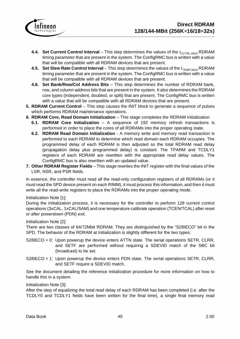
Data Book 45 2.00
Direct RDRAM128/144-MBit (256K×16/18×32s)
4.4. Set Current Control Interval – This step determines the values of the tCCTRL,MAX RDRAMtiming parameter that are present in the system. The ConfigRMC bus is written with a valuethat will be compatible with all RDRAM devices that are present.
4.5. Set Slew Rate Control Interval – This step determines the values of the tTEMP,MAX RDRAMtiming parameter that are present in the system. The ConfigRMC bus is written with a valuethat will be compatible with all RDRAM devices that are present.
4.6. Set Bank/Row/Col Address Bits – This step determines the number of RDRAM bank,row, and column address bits that are present in the system. It also determines the RDRAMcore types (independent, doubled, or split) that are present. The ConfigRMC bus is writtenwith a value that will be compatible with all RDRAM devices that are present.
5. RDRAM Current Control – This step causes the INIT block to generate a sequence of pulseswhich performs RDRAM maintenance operations.
6. RDRAM Core, Read Domain Initialization – This stage completes the RDRAM initialization6.1. RDRAM Core Initialization – A sequence of 192 memory refresh transactions is
performed in order to place the cores of all RDRAMs into the proper operating state.6.2. RDRAM Read Domain Initialization - A memory write and memory read transaction is
performed to each RDRAM to determine which read domain each RDRAM occupies. Theprogrammed delay of each RDRAM is then adjusted so the total RDRAM read delay(propagation delay plus programmed delay) is constant. The TPARM and TCDLY1registers of each RDRAM are rewritten with the appropriate read delay values. TheConfigRMC bus is also rewritten with an updated value.
7. Other RDRAM Register Fields – This stage rewrites the INIT register with the final values of theLSR, NSR, and PSR fields.
In essence, the controller must read all the read-only configuration registers of all RDRAMs (or itmust read the SPD device present on each RIMM), it must process this information, and then it mustwrite all the read-write registers to place the RDRAMs into the proper operating mode.
Initialization Note [1]:During the initialization process, it is necessary for the controller to perform 128 current controloperations (3xCAL, 1xCAL/SAM) and one temperature calibrate operation (TCEN/TCAL) after resetor after powerdown (PDN) exit.
Initialization Note [2]:There are two classes of 64/72Mbit RDRAM. They are distinguished by the “S28IECO” bit in theSPD. The behavior of the RDRAM at initialization is slightly different for the two types:
S28IECO = 0: Upon powerup the device enters ATTN state. The serial operations SETR, CLRR,and SETF are performed without requiring a SDEVID match of the SBC bit(broadcast) to be set.
S28IECO = 1: Upon powerup the device enters PDN state. The serial operations SETR, CLRR,and SETF require a SDEVID match.
See the document detailing the reference initialization procedure for more information on how tohandle this in a system.
Initialization Note [3]:After the step of equalizing the total read delay of each RDRAM has been completed (i.e. after theTCDLY0 and TCDLY1 fields have been written for the final time), a single final memory read

Direct RDRAM128/144-MBit (256K×16/18×32s)
Data Book 46 2.00
transaction should be made to each RDRAM in order to ensure that the output pipeline stages havebeen cleared.
Initialization Note [4]:The SETF command (in the serial SRQ packet) should only be issued once during the Initializationprocess, as should the SETR and CLRR commands.
Initialization Note [5]:The CLRR command (in the serial SRQ packet) leaves some of the contents of the memory core inan indeterminate state.
Control Register Summary
Table 17 summarizes the RDRAM control registers. Detail is provided for each control register inFigure 27 through Figure 43. Read-only bits which are shaded gray are unused and return zero.Read-write bits which are shaded gray are reserved and should always be written with zero. TheRIMM SPD Application Note (DL-0054) describes additional read-only configuration registers whichare present on Direct RIMMs.
The state of the register fields are potentially affected by the IO Reset operation or the SETR/CLRRoperation. This is indicated in the text accompanying each register diagram.
Table 17 Control Register Summary
SA11…SA0 Register Field read-write/read-only
Description
02116 INIT SDEVID read-write, 6 bits Serial device ID. Device address for control register read/write.
PSX read-write, 1 bit Power select exit. PDN/NAP exit with device addr on DQA5 … 0.
SRP read-write, 1 bit SIO repeater. Used to initialize RDRAM.
NSR read-write, 1 bit NAP self-refresh. Enables self-refresh in NAP mode.
PSR read-write, 1 bit PDN self-refresh. Enables self-refresh in PDN mode.
LSR read-write, 1 bit Low power self-refresh. Enables low power self-refresh.
TEN read-write, 1 bit Temperature sensing enable.
TSQ read-write, 1 bit Temperature sensing output.
DIS read-write, 1 bit RDRAM disable.
02216 TEST34 TEST34 read-write, 16 bits Test register. Do not read or write after SIO reset.
02316 CNFGA REFBIT read-only, 3 bit Refresh bank bits. Used for multi-bank refresh.
DBL read-only, 1 bit Double. Specifies doubled-bank architecture
MVER read-only, 6 bit Manufacturer version. Manufacturer identification number.
PVER read-only, 6 bit Protocol version. Specifies version of Direct protocol supported.

Data Book 47 2.00
Direct RDRAM128/144-MBit (256K×16/18×32s)
02416 CNFGB BYT read-only, 1 bit Byte. Specifies an 8-bit or 9-bit byte size.
DEVTYP read-only, 3 bit Device type. Device can be RDRAM or some other device category.
SPT read-only, 1 bit Split-core. Each core half is an individual dependent core.
CORG read-only, 6 bit Core organization. Bank, row, column address field sizes.
SVER read-only, 6 bit Stepping version. Mask version number.
04016 DEVID DEVID read-write, 5 bits Device ID. Device address for memory read/write.
04116 REFB REFB read-write, 4 bits Refresh bank. Next bank to be refreshed by self-refresh.
04216 REFR REFR read-write, 9 bits Refresh row. Next row to be refreshed by REFA, self-refresh.
04316 CCA CCA read-write, 7 bits Current control A. Controls IOL output current for DQA.
ASYMA read-write, 2 bits Asymmetry control. Controls asymmetry of VOL/VOH swing for DQA.
04416 CCB CCB read-write, 7 bits Current control B. Controls IOL output current for DQB.
ASYMB read-write, 2 bits Asymmetry control. Controls asymmetry of VOL/VOH swing for DQB.
04516 NAPX NAPXA read-write, 5 bits NAP exit. Specifies length of NAP exit phase A.
NAPX read-write, 5 bits NAP exit. Specifies length of NAP exit phase A + phase B.
DQS read-write, 1 bits DQ select. Selects CMD framing for NAP/PDN exit.
04616 PDNXA PDNXA read-write, 13 bits PDN exit. Specifies length of PDN exit phase A.
04716 PDNX PDNX read-write, 13 bits PDN exit. Specifies length of PDN exit phase A + phase B.
04816 TPARM TCAS read-write, 2 bits tCAS-C core parameter. Determines tOFFP data sheet parameter.
TCLS read-write, 2 bits tCLS-C core parameter. Determines tCAC and tOFFP parameters.
TCDLY0 read-write, 3 bits tCDLY0-C core parameter. Programmable delay for read data.
04916 TFRM TFRM read-write, 4 bits tFRM-C core parameter. Determines ROW-COL packet framing interval.
04a16 TCDLY1 TCDLY1 read-write, 3 bits tCDLY1-C core parameter. Programmable delay for read data.
04c16 TCYCLE TCYCLE read-write, 14 bits tCYCLE data sheet parameter. Specifies cycle time in 64 ps units.
Table 17 Control Register Summary (cont’d)
SA11…SA0 Register Field read-write/read-only
Description

Direct RDRAM128/144-MBit (256K×16/18×32s)
Data Book 48 2.00
04b16 SKIP AS read-only, 1 bit Autoskip value established by the SETF command.
MSE read-write, 1 bit Manual skip enable. Allows the MS value to override the AS value.
MS read-write, 1 bit Manual skip value.
04d16- TEST77 TEST77 read-write, 16 bits Test register. Write with zero after SIO reset.
04e16- TEST78 TEST78 read-write, 16 bits Test register. Do not read or write after SIO reset.
04f16- TEST79 TEST79 read-write, 16 bits Test register. Do not read or write after SIO reset.
08016 - 0ff16 reserved reserved vendor-specific Vendor-specific test registers. Do not read or write after SIO reset.
Table 17 Control Register Summary (cont’d)
SA11…SA0 Register Field read-write/read-only
Description
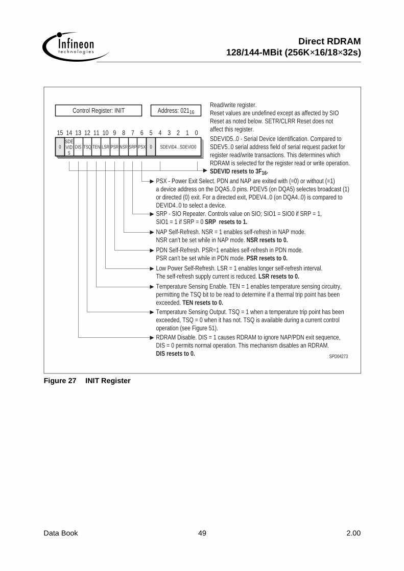
Data Book 49 2.00
Direct RDRAM128/144-MBit (256K×16/18×32s)
Figure 27 INIT Register
0
15 14 13 12 11 10 9 8 7 6 5 4 3 2 1 0
Control Register: INIT
SDEVID5
DIS TSQ TEN LSR PSR NSR SRP PSX 0 SDEVID4...SDEVID0
SPD04273
Address: 02116
PSX - Power Exit Select. PDN and NAP are exited with (=0) or without (=1)a device address on the DQA5..0 pins. PDEV5 (on DQA5) selectes broadcast (1)or directed (0) exit. For a directed exit, PDEV4..0 (on DQA4..0) is compared toDEVID4..0 to select a device.SRP - SIO Repeater. Controls value on SIO; SIO1 = SIO0 if SRP = 1,SIO1 = 1 if SRP = 0 SRP resets to 1.
NAP Self-Refresh. NSR = 1 enables self-refresh in NAP mode.NSR can’t be set while in NAP mode. NSR resets to 0.
PDN Self-Refresh. PSR=1 enables self-refresh in PDN mode.PSR can’t be set while in PDN mode. PSR resets to 0.
Low Power Self-Refresh. LSR = 1 enables longer self-refresh interval.The self-refresh supply current is reduced. LSR resets to 0.
Temperature Sensing Enable. TEN = 1 enables temperature sensing circuitry,permitting the TSQ bit to be read to determine if a thermal trip point has beenexceeded. TEN resets to 0.Temperature Sensing Output. TSQ = 1 when a temperature trip point has beenexceeded, TSQ = 0 when it has not. TSQ is available during a current controloperation (see Figure 51).RDRAM Disable. DIS = 1 causes RDRAM to ignore NAP/PDN exit sequence,DIS = 0 permits normal operation. This mechanism disables an RDRAM.DIS resets to 0.
SDEVID5..0 - Serial Device Identification. Compared toSDEV5..0 serial address field of serial request packet forregister read/write transactions. This determines whichRDRAM is selected for the register read or write operation.SDEVID resets to 3F 16.
Read/write register.Reset values are undefined except as affected by SIOReset as noted below. SETR/CLRR Reset does notaffect this register.

Direct RDRAM128/144-MBit (256K×16/18×32s)
Data Book 50 2.00
Figure 28 CNFGA Register
Figure 29 CNFGB Register
15 14 13 12 11 10 9 8 7 6 5 4 3 2 1 0
Control Register: CNFGA
PVER5...0= 000001
MVER5...0= mmmmmm
REFBIT2...0= 100
DBL1
Address: 02316
DBL - Doubled-Bank. DBL = 1 means the device uses adoubled-bank architecture with adjacent-bankdependency. DBL = 0 means no dependency.MVER5..0 - Manufacturer Version. Specifies themanufacturer identification number.
PVER5..0 - Protocol Version. Specifies the DirectProtocol version used by this device:0 - Compliant with version 0.62.1 - Compliant with version 0.7 through this version.2 to 63 - Reserved.
Read-only register.
REFBIT2..0 - Refresh Bank Bits. Specifies the numberof bank address bits used by REFA and REFPcommands. Permits multi-bank refresh in futureRDRAMs.
Note: In RDRAMs with protocol version 1 PVER[5:0] = 000001,the range of the PDNX field (PDNX[2:0] in the PDNX register)may not be large enough to specify the location of the restrictedinterval in Figure 47. In this case, the effective tS4 parameter mustincrease and no row or column packets may overlap therestricted interval. See Figure 47 and Table 19.
SPD04274
15 14 13 12 11 10 9 8 7 6 5 4 3 2 1 0
Control Register: CNFGB
SVER5...0= ssssss
CORG4...0= xxxxx
DEVTYP2...0= 000
SPT1
BYTB
Address: 02416
DEVTYP2..0 - Device type. DEVTYP = 000 meansthat this device is an RDRAM.
BYT - Byte width. B = 1 means the device readsand writes 9-bit memory bytes. B = 0 means 8 bits.
CORG4..0 - Core organization. This field specifiesthe number of bank (3, 4, 5, or 6 bits), row(9, 10, 11, or 12 bits), and column (5, 6, or 7 bits)address bits. The encoding of this field will bespecified in a later version of this document.
SVER5..0 - Stepping version. Specifies the maskversion number of this device.
SPT - Split-core. SPT = 1 means the core is split,SPT = 0 means it is not.
Read-only register.
SPD04255

Data Book 51 2.00
Direct RDRAM128/144-MBit (256K×16/18×32s)
Figure 30 TEST Register
Figure 31 DEVID Register
11
0
14
0 0
15
0 0
13 12
Address: 02216Control Register: TEST34
0 0
10 9
00 0
78 6 3
00 0
5 4
0 0
2 1
0
0
Read/write registers.Reset value of TEST34 is zero ( from SIO Reset).This register are used for testing purposes. It mustnot be read or written after SIO Reset.
SPD04276
11
0
14
0 0
15
0 0
13 12
Address: 04016Control Register: DEVID
0 0
10 9
00 0
78 6 3
0
5 4
DEVID4...DEVID0
2 1 0
Read/write register.Reset value is undefined.Device Identification register.DEVID4..DEVID0 is compared to DR4..DR0,DC4..DC0, and DX4..DX0 fields for all memoryread or write transactions. This determines whichRDRAM is selected for the memory read or writetransaction. SPD04277
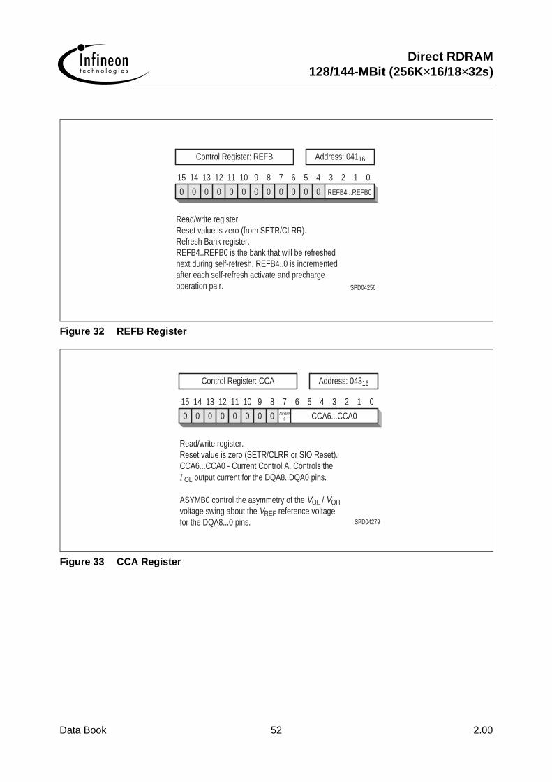
Direct RDRAM128/144-MBit (256K×16/18×32s)
Data Book 52 2.00
Figure 32 REFB Register
Figure 33 CCA Register
11
0
14
0 0
15
0 0
13 12
Address: 04116Control Register: REFB
0 0
10 9
00 0
78 6 3
0 0
5 4 2 0
Read/write register.Reset value is zero (from SETR/CLRR).Refresh Bank register.REFB4..REFB0 is the bank that will be refreshednext during self-refresh. REFB4..0 is incrementedafter each self-refresh activate and prechargeoperation pair.
REFB4...REFB0
1
SPD04256
11
0
14
0 0
15
0 0
13 12
Address: 04316Control Register: CCA
0 0
10 9ASYMA
00
78 6 35 4 2 0
Read/write register.Reset value is zero (SETR/CLRR or SIO Reset).CCA6...CCA0 - Current Control A. Controls theI OL output current for the DQA8..DQA0 pins.
ASYMB0 control the asymmetry of the VOL / VOHvoltage swing about the VREF reference voltagefor the DQA8...0 pins.
CCA6...CCA0
1
SPD04279

Data Book 53 2.00
Direct RDRAM128/144-MBit (256K×16/18×32s)
Figure 34 REFR Register
Figure 35 CCB Register
11
0
14
0 0
15
0 0
13 12
Address: 04216Control Register: REFR
0 0
10 9 78 6 35 4 2 0
Read/write register.Reset value is zero (from SETR/CLRR).Refresh Row register.REFR8...REFR0 is the row that will be refreshednext by the REFA command or by self-refresh.REFR8...0 is incremented when BR4...0 = 1111 forthe REFA command. REFR8...0 is incrementedwhen REFB4...0 = 1111 for self-refresh.
REFR8...REFR0
1
SPD04257
Read/write register.Reset value is zero (SETR/CLRR or SIO Reset).CCB6...CCB0 - Current Control B. Controls the IOLoutput current for the DQB8...DQB0 pins.
ASYMB0 control the asymmetry of the VOL / VOHvoltage swing about the VREF reference voltagefor the DQB8...0 pins.
11
0
14
0 0
15
0 0
13 12
Address: 04416Control Register: CCB
0 0
10 9ASYMB
00
78 6 35 4 2 0
CCB6...CCB0
1
SPD04281

Direct RDRAM128/144-MBit (256K×16/18×32s)
Data Book 54 2.00
Figure 36 NAPX Register
Figure 37 PDNXA Register
15 14 13 12 11 10 9 8 7 6 5 4 3 2 1 0
Control Register: NAPX
NAPX4..0 NAPXA4..0
Address: 04516
NAPXA4...0 - Nap Exit Phase A. This field speci-fies the number of SCK cycles during the firstphase for exiting NAP mode. It must satisfy:
NAPXA * tSCYCLE ≥ tNAPXA,MAXDo not set this field to zero.
NAPX4...0 - Nap Exit Phase A plus B. This field specifiesthe number of SCK cycles during the first plus secondphases for exiting NAP mode. It must satisfy:
NAPX * tSCYCLE ≥ NAPXA * tSCYCLE + tNAPXB,MAXDo not set this field to zero.
DQS - DQ Select. This field specifies the number of SCKcycles (0 => 0.5 cycles, 1 => 1.5 cycles) between theCMD pin framing sequence and the device selectionon DQ5...0. See Figure 48 - This field must be writtenwith a “1” for this RDRAM.
Read/write register.Reset value is undefined
Note - tSCYCLE is tCYCLE1 (SCK cycle time).0 DQS0 0 0 0
SPD04282
1114
0 0
15
0
13 12
Address: 04616Control Register: PDNXA
10 9
PDNXA12...0
78 6 35 4 2 1 0
Read/write register.Reset value is undefinedPDNXA4...0 - PDN Exit Phase A. This field specifiesthe number of (64 * SCK cycle) units duringthe first phase for exiting PDN mode. It mustsatisfy:PDNXA * 64 * tSCYCLE ≥ tPDNXA, MAXDo not set this field to zero.Note - only PDNXA5...0 are implemented.Note - tSCYCLE is tCYCLE1 (SCK cycle time).
SPD04283
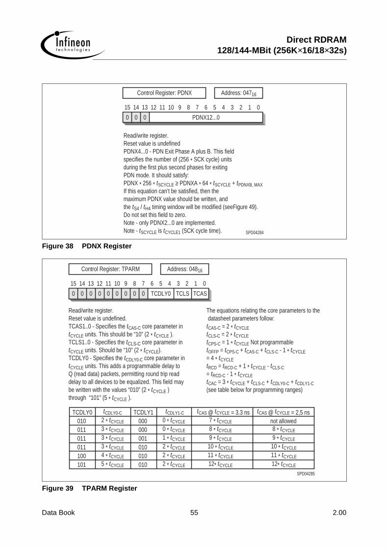
Data Book 55 2.00
Direct RDRAM128/144-MBit (256K×16/18×32s)
Figure 38 PDNX Register
Figure 39 TPARM Register
1114
0 0
15
0
13 12
Address: 04716Control Register: PDNX
10 9
PDNX12...0
78 6 35 4 2 1 0
Read/write register.Reset value is undefinedPDNX4...0 - PDN Exit Phase A plus B. This fieldspecifies the number of (256 * SCK cycle) unitsduring the first plus second phases for exitingPDN mode. It should satisfy:PDNX * 256 * tSCYCLE ≥ PDNXA * 64 * tSCYCLE + tPDNXB, MAXIf this equation can’t be satisfied, then themaximum PDNX value should be written, andthe tS4 / tH4 timing window will be modified (seeFigure 49).Do not set this field to zero.Note - only PDNX2...0 are implemented.Note - tSCYCLE is tCYCLE1 (SCK cycle time). SPD04284
11
0
14
0 0
15
0 0
13 12
Address: 04816Control Register: TPARM
0 0
10 9
00
78 6 3
TCDLY0
5 4
TCLS
2 1
TCAS
0
Read/write register.Reset value is undefined.TCAS1..0 - Specifies the tCAS-C core parameter intCYCLE units. This should be “10” (2 * tCYCLE ).TCLS1..0 - Specifies the tCLS-C core parameter intCYCLE units. Should be “10” (2 * tCYCLE).TCDLY0 - Specifies the tCDLY0-C core parameter intCYCLE units. This adds a programmable delay toQ (read data) packets, permitting round trip readdelay to all devices to be equalized. This field maybe written with the values “010” (2 * tCYCLE )through “101” (5 * tCYCLE ).
The equations relating the core parameters to thedatasheet parameters follow:tCAS-C = 2 * tCYCLEtCLS-C = 2 * tCYCLEtCPS-C = 1 * tCYCLE Not programmabletOFFP = tCPS-C + tCAS-C + tCLS-C - 1 * tCYCLE= 4 * tCYCLEtRCD = tRCD-C + 1 * tCYCLE - tCLS-C= tRCD-C - 1 * tCYCLEtCAC = 3 * tCYCLE + tCLS-C + tCDLY0-C + tCDLY1-C(see table below for programming ranges)
TCDLY0 TCDLY1010 000 not allowed
tCDLY0-C tCDLY1-C
7 * tCYCLE0 * tCYCLE2 * tCYCLE
011 000 8 * tCYCLE0 * tCYCLE3 * tCYCLE
011 001 9 * tCYCLE1 * tCYCLE3 * tCYCLE
011 010 10 * tCYCLE2 * tCYCLE3 * tCYCLE
100 010 11 * tCYCLE2 * tCYCLE4 * tCYCLE
101 010 12* tCYCLE
8 * tCYCLE
9 * tCYCLE
10 * tCYCLE
11 * tCYCLE
12* tCYCLE2 * tCYCLE5 * tCYCLE
tCAS @ tCYCLE = 3.3 ns tCAS @ tCYCLE = 2,5 ns
SPD04285

Direct RDRAM128/144-MBit (256K×16/18×32s)
Data Book 56 2.00
Figure 40 TFRM Register
Figure 41 TRDLY Register
11
0
14
0 0
15
0 0
13 12
Address: 04916Control Register: TFRM
0 0
10 9
00 0
78 6 3
0 0
5 4 2 0
Read/write register.Reset value is undefined.TFRM3...0 - Specifies the position of the framingpoint in tCYCLE units. This value must be greateror equal to the tFRM,MIN parameter. This isthe minimum offset between a ROW packet(which places a device at ATTN) and the firstCOL packet (directed to that device) which mustbe framed. This field may be written with thevalues “0111” (7 * tCYCLE ) through “1010”(10 * tCYCLE ). TFRM is usually set to the valuewhich matches the largest tRCD,MIN parameter(modulo 4 * tCYCLE) that is present in an RDRAMin the memory system. Thus, if an RDRAM withtRCD, MIN = 11 * tCYCLE were present, then TFRMwould be programmed to 7 * tCYCLE .
TFRM3...0
1
SPD04286
11
0
14
0 0
15
0 0
13 12
Address: 04A16Control Register: TCDLY1
0 0
10 9
00 0
78 6 3
0 0 0
5 4 2 0
Read/write register.Reset value is undefined.TCDLY1 - Specifies the value of the tCDLY1-C coreparameter in tCYCLE units. This adds a programm-able delay to Q (read data) packets, permittinground trip read delay to all devices to be equalized. This field may be written with the values“000” (0 * tCYCLE ) through “010” (2 * tCYCLE ). Referto Figure 39 for more details.
TCDLY1
1
SPD04287

Data Book 57 2.00
Direct RDRAM128/144-MBit (256K×16/18×32s)
Figure 42 SKIP Register
Figure 43 TEST Registers
11
MSE
14
0 0
15
0 AS
13 12
Address: 04B16Control Register: SKIP
MS 0
10 9
00 0
78 6 3
00 0
5 4
0 0
2 1
0
0
Read/write register (except AS field).Reset value is zero (SIO Reset).AS - Autoskip. Read-only value determined byautoskip circuit and stored when SETF serialcommand is received by RDRAM during initial-ization.In figure 58, AS = 1 corresponds to theearly Q(a1) packet and AS = 0 to the Q(a1) packetone tCYCLE later for the four uncertain cases.MSE - Manual skip enable (0 = auto, 1 = manual).MS - Manual skip (MS must be 1 when MSE = 1).>During initialization, the RDRAMs at the furthestpoint in the fifth read domain may have selectedthe AS = 0 value, placing them at the closest pointin a sixth read domain. Setting the MSE/MS fieldsto 1/1 overrides the autoskip value and returnsthem to the furthest point of the fifth readdomain. SPD04288
11
0
14
0 0
15
0 0
13 12
Address: 04F16Control Register: TEST79
Address: 04E16Control Register: TEST78
Address: 04D16Control Register: TEST77
0 0
10 9
00 0
78 6 3
00 0
5 4
0 0
2 1
0
0
Read/write registers.Reset value of TEST78, 79 is zero ( SIO Reset).Do not read or write TEST78, 79 after SIO reset.TEST77 must be written with zero after SIO reset.These registers must only be used for testingpurposes. SPD04289

Direct RDRAM128/144-MBit (256K×16/18×32s)
Data Book 58 2.00
Figure 44 TCYCLE Register
Power State Management
Table 18 summarizes the power states available to a Direct RDRAM. In general, the lowest powerstates have the longest operational latencies. For example, the relative power levels of PDN stateand STBY state have a ratio of about 1:110, and the relative access latencies to get read data havea ratio of about 250:1.
PDN state is the lowest power state available. The information in the RDRAM core is usuallymaintained with self-refresh; an internal timer automatically refreshes all rows of all banks. PDN hasa relatively long exit latency because the TCLK/RCLK block must resynchronize itself to the externalclock signal.
NAP state is another low-power state in which either self-refresh or REFA-refresh are used tomaintain the core. See “Refresh” on page 64 for a description of the two refresh mechanisms. NAPhas a shorter exit latency than PDN because the TCLK/RCLK block maintains its synchronizationstate relative to the external clock signal at the time of NAP entry. This imposes a limit (tNLIMIT) onhow long an RDRAM may remain in NAP state before briefly returning to STBY or ATTN to updatethis synchronization state.
Table 18 Power State Summary
PowerState
Description Blocks Consuming Power
PowerState
Description Blocks Consuming Power
PDN Powerdown state. Self-refresh NAP Nap state. Similar to PDN except lower wake-up latency.
Self-refresh or REFA-refreshTCLK/RCLK-Nap
STBY Standby state.Ready for ROWpackets.
REFA-refreshTCLK/RCLKROW demux receiver
ATTN Attention state.Ready for ROW and COL packets.
REFA-refreshTCLK/RCLKROW demux receiverCOL demux receiver
ATTNR Attention read state.Ready for ROW and COL packets.Sending Q (read data) packets.
REFA-refreshTCLK/RCLKROW demux receiverCOL demux receiverDQ mux transmitterCore power
ATTNW Attention write state.Ready for ROW and COL packets.Ready for D (write data) packets.
REFA-refreshTCLK/RCLKROW demux receiverCOL demux receiverDQ demux receiverCore power
1114
0 0
15 13 12
Address: 04C16Control Register: TCYCLE
10 9
TCYCLE13...TCYCLE0
78 6 35 4 2 1 0
Read/write register.Reset value is undefinedTCYCLE13...0 - Specifies the value of the tCYCLEdatasheet parameter in 64 ps units. For thetCYCLE, MIN of 2.5 ns (2500 ps), this field should bewritten with the value “00027 16 ” (39 * 64 ps). SPD04290
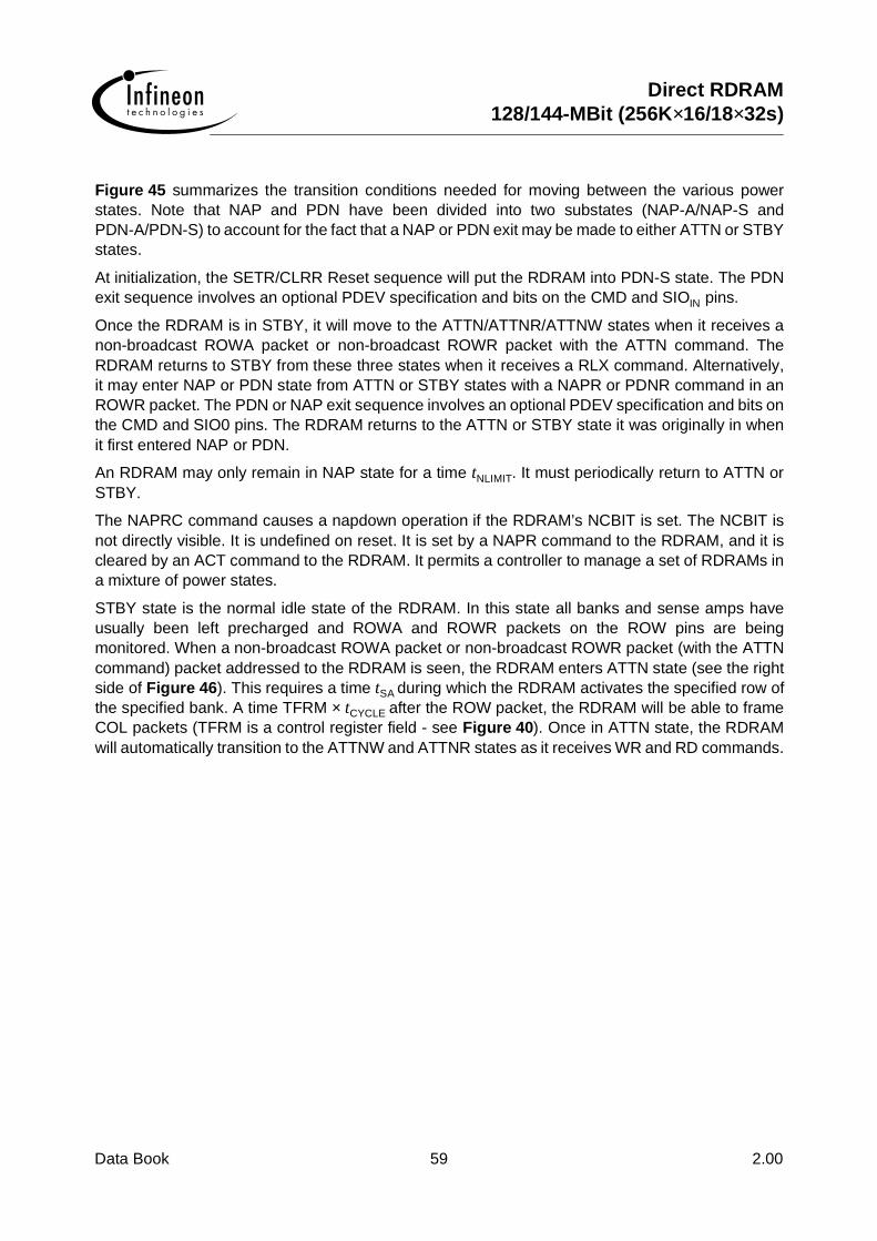
Data Book 59 2.00
Direct RDRAM128/144-MBit (256K×16/18×32s)
Figure 45 summarizes the transition conditions needed for moving between the various powerstates. Note that NAP and PDN have been divided into two substates (NAP-A/NAP-S andPDN-A/PDN-S) to account for the fact that a NAP or PDN exit may be made to either ATTN or STBYstates.
At initialization, the SETR/CLRR Reset sequence will put the RDRAM into PDN-S state. The PDNexit sequence involves an optional PDEV specification and bits on the CMD and SIOIN pins.
Once the RDRAM is in STBY, it will move to the ATTN/ATTNR/ATTNW states when it receives anon-broadcast ROWA packet or non-broadcast ROWR packet with the ATTN command. TheRDRAM returns to STBY from these three states when it receives a RLX command. Alternatively,it may enter NAP or PDN state from ATTN or STBY states with a NAPR or PDNR command in anROWR packet. The PDN or NAP exit sequence involves an optional PDEV specification and bits onthe CMD and SIO0 pins. The RDRAM returns to the ATTN or STBY state it was originally in whenit first entered NAP or PDN.
An RDRAM may only remain in NAP state for a time tNLIMIT. It must periodically return to ATTN orSTBY.
The NAPRC command causes a napdown operation if the RDRAM’s NCBIT is set. The NCBIT isnot directly visible. It is undefined on reset. It is set by a NAPR command to the RDRAM, and it iscleared by an ACT command to the RDRAM. It permits a controller to manage a set of RDRAMs ina mixture of power states.
STBY state is the normal idle state of the RDRAM. In this state all banks and sense amps haveusually been left precharged and ROWA and ROWR packets on the ROW pins are beingmonitored. When a non-broadcast ROWA packet or non-broadcast ROWR packet (with the ATTNcommand) packet addressed to the RDRAM is seen, the RDRAM enters ATTN state (see the rightside of Figure 46). This requires a time tSA during which the RDRAM activates the specified row ofthe specified bank. A time TFRM × tCYCLE after the ROW packet, the RDRAM will be able to frameCOL packets (TFRM is a control register field - see Figure 40). Once in ATTN state, the RDRAMwill automatically transition to the ATTNW and ATTNR states as it receives WR and RD commands.

Direct RDRAM128/144-MBit (256K×16/18×32s)
Data Book 60 2.00
Figure 45 Power State Transition Diagram
Once the RDRAM is in ATTN, ATTNW, or ATTNR states, it will remain there until it is explicitlyreturned to the STBY state with a RLX command. A RLX command may be given in an ROWR,COLC, or COLX packet (see the left side of Figure 46). It is usually given after all banks of theRDRAM have been precharged; if other banks are still activated, then the RLX command wouldprobably not be given.
If a broadcast ROWA packet or ROWR packet (with the ATTN command) is received, the RDRAM’spower state doesn’t change. If a broadcast ROWR packet with RLXR command is received, theRDRAM goes to STBY.
SPD04231
ATTNR
ATTNAu
tom
atic
Auto
mat
ic
Automatic
AutomaticATTNW
NAP-A
Auto
mat
ic
Auto
mat
ic
NAP-S
NAPPDEV.CMD x SIO0
NAPR x RLXR
NAPR x RLXR
PDEV.CMD x SIO0
STBY
PDN-S
PDN-A
PDN
PDNR
NAPR
ATTN
PDNR x RLXR
PDEV.CMD x SIO0
PDNR x RLXR
PDEV.CMD x SIO0
RLX
SETR/CLRR
NLIMITt
Notation:SETR/CLRRPDNRNAPRRLXRRLXSIO0PDEV.CMDATTN
(Non-Broadcast) with ATTN Command
- SETR/CLRR Reset Sequence in SRQ Packets
- ROWA Packet (Non-Broadcast) or ROWR Packet
- RLX Command in ROWR, COLC, COLX Packets- RLX Command in ROWR Packet- NAPR Command in ROWR Packet- PDNR Command in ROWR Packet
- (PDEV = DEVID) x (CMD = 01)- SIO0 Input Value

Data Book 61 2.00
Direct RDRAM128/144-MBit (256K×16/18×32s)
Figure 47 shows the NAP entry sequence (left). NAP state is entered by sending a NAPRcommand in a ROW packet. A time tASN is required to enter NAP state (this specification is providedfor power calculation purposes). The clock on CTM/CFM must remain stable for a time tCD after theNAPR command.
The RDRAM may be in ATTN or STBY state when the NAPR command is issued. When NAP stateis exited, the RDRAM will return to the original starting state (ATTN or STBY). If it is in ATTN stateand a RLXR command is specified with NAPR, then the RDRAM will return to STBY state whenNAP is exited.
Figure 47 also shows the PDN entry sequence (right). PDN state is entered by sending a PDNRcommand in a ROW packet. A time tASP is required to enter PDN state (this specification is providedfor power calculation purposes). The clock on CTM/CFM must remain stable for a time tCD after thePDNR command.
The RDRAM may be in ATTN or STBY state when the PDNR command is issued. When PDN stateis exited, the RDRAM will return to the original starting state (ATTN or STBY). If it is in ATTN stateand a RLXR command is specified with PDNR, then the RDRAM will return to STBY state whenPDN is exited. The current- and slew-rate-control levels are re-established.
The RDRAM’s write buffer must be retired with the appropriate COP command before NAP or PDNare entered. Also, all the RDRAM’s banks must be precharged before NAP or PDN are entered. Theexception to this is if NAP is entered with the NSR bit of the INIT register cleared (disablingself-refresh in NAP). The commands for relaxing, retiring, and precharging may be given to theRDRAM as late as the ROPa0, COPa0, and XOPa0 packets in Figure 47. No broadcast packetsnor packets directed to the RDRAM entering Nap or PDN may overlay the quiet window. Thiswindow extends for a time tNPQ after the packet with the NAPR or PDNR command.
Figure 48 shows the NAP and PDN exit sequences. These sequences are virtually identical; theminor differences will be highlighted in the following description.
Before NAP or PDN exit, the CTM/CFM clock must be stable for a time tCE. Then, on a falling andrising edge of SCK, if there is a “01” on the CMD input, NAP or PDN state will be exited. Also, on thefalling SCK edge the SIO0 input must be at a 0 for NAP exit and 1 for PDN exit.
If the PSX bit of the INIT register is 0, then a device PDEV5 … 0 is specified for NAP or PDN exiton the DQA5 … 0 pins. This value is driven on the rising SCK edge 0.5 or 1.5 SCK cycles after theoriginal falling edge, depending upon the value of the DQS bit of the NAPX register. If the PSX bitof the INIT register is 1, then the RDRAM ignores the PDEV5 … 0 address packet and exits NAP orPDN when the wake-up sequence is presented on the CMD wire. The ROW and COL pins must bequiet at a time tS4/tH4 around the indicated falling SCK edge (timed with the PDNX or NAPX registerfields). After that, ROW and COL packets may be directed to the RDRAM which is now in ATTN orSTBY state.
Figure 49 shows the constraints for entering and exiting NAP and PDN states. On the left side, anRDRAM exits NAP state at the end of cycle T3. This RDRAM may not re-enter NAP or PDN statefor an interval of tNU0. The RDRAM enters NAP state at the end of cycle T13. This RDRAM may notre-exit NAP state for an interval of tNU1. The equations for these two parameters depend upon anumber of factors, and are shown at the bottom of the figure. NAPX is the value in the NAPX fieldin the NAPX register.
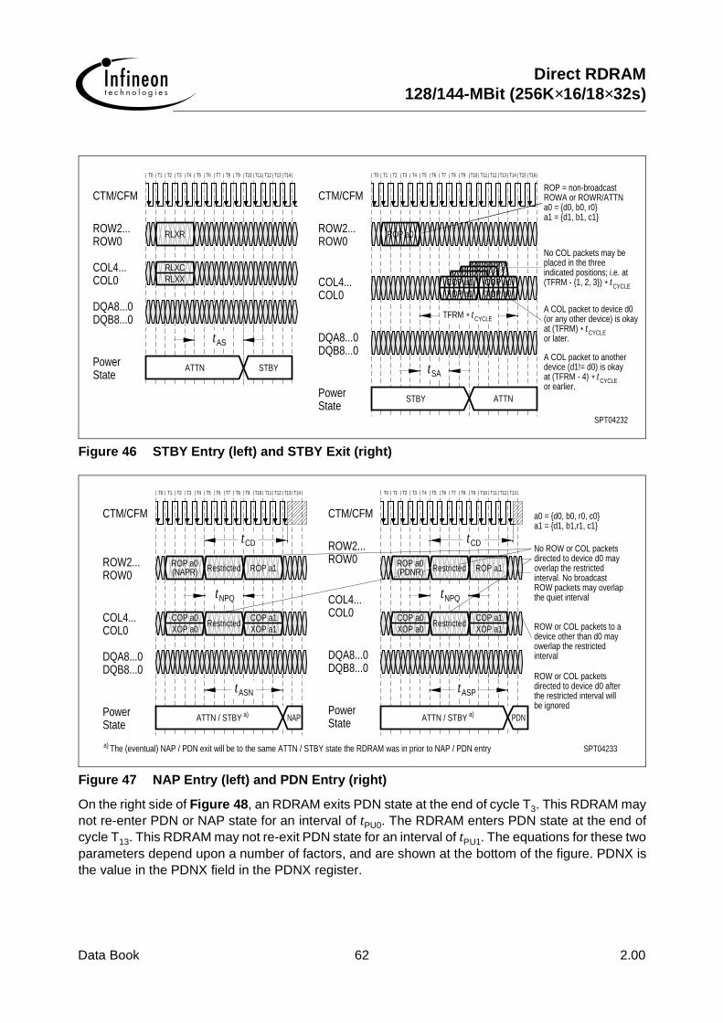
Direct RDRAM128/144-MBit (256K×16/18×32s)
Data Book 62 2.00
Figure 46 STBY Entry (left) and STBY Exit (right)
Figure 47 NAP Entry (left) and PDN Entry (right)
On the right side of Figure 48, an RDRAM exits PDN state at the end of cycle T3. This RDRAM maynot re-enter PDN or NAP state for an interval of tPU0. The RDRAM enters PDN state at the end ofcycle T13. This RDRAM may not re-exit PDN state for an interval of tPU1. The equations for these twoparameters depend upon a number of factors, and are shown at the bottom of the figure. PDNX isthe value in the PDNX field in the PDNX register.
at (TFRM)
ATTNPowerState
tAS
STBY
State
DQB8...0DQA8...0
Powert
CYCLE
SPT04232
device (d1!= d0) is okayA COL packet to another
STBY ATTN
SAtor earlier.at (TFRM - 4) *
t*
CYCLE
ROP a0
CTM/CFM
ROW2...ROW0
COL4...COL0
DQB8...0DQA8...0
RLXXRLXC
RLXR
T0 T3T1 T2 T4 T5
COL4...COL0
ROW2...
CTM/CFM
ROW0
T8T6 T7 T9 T10 T13T11 T12 T14 T0 T1 T2
A COL packet to device d0(or any other device) is okay
a1 = d1, b1, c1
ROWA or ROWR/ATTNROP = non-broadcast
No COL packets may beplaced in the threeindicated positions; i.e. at(TFRM - 1, 2, 3)COP a0
XOP a0
TFRM
COP a1XOP a1
* tCYCLE
a0 = d0, b0, r0
T5T4T3 T6 T7 T10T9T8 T11 T12 T15T14T13 T16
CYCLEt*
or later.
owerlap the restricted
The (eventual) NAP / PDN exit will be to the same ATTN / STBY state the RDRAM was in prior to NAP / PDN entry
PowerState
a)
DQA8...0DQB8...0
NAPa)ATTN / STBY
ASNt
StatePower
DQA8...0DQB8...0
SPT04233
the restricted interval willdirected to device d0 afterROW or COL packets
ATTN / STBY a)
ASPt
PDN
interval
be ignored
ROP a0
COP a0XOP a0
(NAPR)
COL0COL4...
ROW0ROW2...
CTM/CFM
T0 T1 T2 T3
Restricted ROP a1
Restricted
NPQt
XOP a1COP a1
tCD
COL0COL4...
ROW0
CTM/CFM
ROW2...
T6T5T4 T7 T8 T11T10T9 T12 T13 T14 T0
No ROW or COL packetsdirected to device d0 mayoverlap the restrictedinterval. No broadcastROW packets may overlapthe quiet interval
device other than d0 mayROW or COL packets to a
a1 = d1, b1,r1, c1a0 = d0, b0, r0, c0
COP a1XOP a1
ROP a1Restricted(PDNR)
RestrictedXOP a0COP a0
NPQt
ROP a0
CDt
T3T1 T2 T4 T5 T8T6 T7 T9 T10 T13T11 T12

Data Book 63 2.00
Direct RDRAM128/144-MBit (256K×16/18×32s)
Figure 48 NAP and PDN Exit
t
Device selection timing slot is selected by DQS field of NAPX register
asserted at NAP or PDN entry time
The DQS field must be written with "1" for this RDRAMExit to STBY or ATTN depends upon whether RLXR wasd)
c)
DQS = 0
from SIO0 to SIO1
NAP / PDN
The packet is repeated
Use 0 for NAP exit, 1 for PDN exit
StatePower
SIO1
b)
a)
0/1
SIO0
CMD
SCK
0/1
0
CE
DQS = 1b b
a
a
1
DQS = 0b
SPT04234
dSTBY / ATTN
*
+ (PDNXA
is exiting the NAP-A or PDN-A statesrestricted interval if device PDEVNo COL packets may overlap the
Effective hold becomes
T24T23T21T20T19T18T16T15 T17T14T13T10 T11 T12T9T8T5 T6 T7T4T3T2T1 T22T0
t
If PSX = 1 in Init register, then NAP/PDNexit is broadcast (no PDEV field).
COL4...COL0
DQA8...0DQB8...0
ROW0
CTM/CFM
ROW2...
DQS = 1b, c
S3
H3tS3
ttH3
< (PDNXAif (PDNX
t t= H4H4
* 64256*
T47T46T45T42 T43T41T40T38T36T35 T37 T39T31T30T28T26T25 T27 T29 T34 T44
XOPCOP
ROP
COPRestricted
PDNXB, MAX
PDNXB, MAX
SCYCLEt*64*
SCYCLE
SCYCLE
* tt
+ t)
t+
S4
)t
XOP
H4t
the restricted intervalNo ROW packets may overlap
S4tH4t
(NAPX SCYCLEt* )* SCYCLEt ) / (256 PDNX *
- (PDNX * 256 * SCYCLEt )
ROP Restricted
).
´
PDEV5...0PDEV5...0 b b

Direct RDRAM128/144-MBit (256K×16/18×32s)
Data Book 64 2.00
Figure 49 NAP Entry/Exit Windows (left) and PDN Entry/Exit Windows (right)
Refresh
RDRAMs, like any other DRAM technology, use volatile storage cells which must be periodicallyrefreshed. This is accomplished with the REFA command. Figure 50 shows an example of this.
The REFA command in the transaction is typically a broadcast command (DR4T and DR4F are bothset in the ROWR packet), so that in all devices bank number Ba is activated with row number REFR,where REFR is a control register in the RDRAM. When the command is broadcast and ATTN is set,the power state of the RDRAMs (ATTN or STBY) will remain unchanged. The controller incrementsthe bank address Ba for the next REFA command. When Ba is equal to its maximum value, theRDRAM automatically increments REFR for the next REFA command.
On average, these REFA commands are sent once every tREF/2BBIT+RBIT (where BBIT are thenumber of bank address bits and RBIT are the number of row address bits) so that each row of eachbank is refreshed once every tREF interval.
The REFA command is equivalent to an ACT command, in terms of the way that it interacts withother packets (see Table 12). In the example, an ACT command is sent after tRR to address b0, adifferent (non-adjacent) bank than the REFA command.
A second ACT command can be sent after a time tRC to address c0, the same bank (or an adjacentbank) as the REFA command.
Note that a broadcast REFP command is issued a time tRAS after the initial REFA command in orderto precharge the refreshed bank in all RDRAMs. After a bank is given a REFA command, no othercore operations (activate or precharge) should be issued to it until it receives a REFP.
It is also possible to interleave refresh transactions (not shown). In the figure, the ACT b0 commandwould be replaced by a REFA b0 command. The b0 address would be broadcast to all devices, and
PDN exitNAP exit
+ (2 + NAPX)
no entry to NAP or PDN
if NSR = 1
CMD
5
8
23NU1
NU1t
t
=
=NU0t = CYCLE
CYCLE
CYCLE*
* t
t
* t
- (0.5
0 1
SCYCLE
) if NSR = 0SCYCLEt*
t*
NU0t NU1no exitt
0 CMD
SCYCLE
PDNX)
no entry to NAP or PDN
SCYCLE
SCYCLE
SCYCLE
5
8
23PU1
PU1
t
t
=
=PU0t =
t*
* t* t
0
*
if PSR = 1
+ (2 + 256
- (0.5 t*
1
PU0t
SPT04235
PU1no exit
) if PSR = 0
* SCYCLEt
t
0
ROW2...
CTM/CFM
ROW0ROW2...
CTM/CFM
SCK
T2T0 T1 T3 T4 T6T5 T7 T18T13
NAP entry
T10T8 T9 T11 T12
NAPR
T14 T15 T17T16 T19
SCK
ROW0
T10T2 T3 T4 T6T5 T7 T9T8
PDN entry
NAPR
T13T11 T12 T14 T15 T17T16 T18 T19
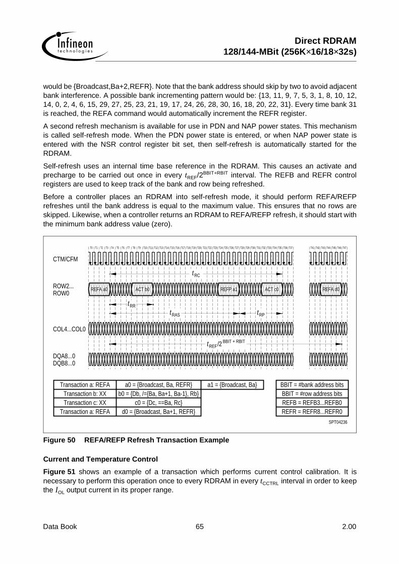
Data Book 65 2.00
Direct RDRAM128/144-MBit (256K×16/18×32s)
would be Broadcast,Ba+2,REFR. Note that the bank address should skip by two to avoid adjacentbank interference. A possible bank incrementing pattern would be: 13, 11, 9, 7, 5, 3, 1, 8, 10, 12,14, 0, 2, 4, 6, 15, 29, 27, 25, 23, 21, 19, 17, 24, 26, 28, 30, 16, 18, 20, 22, 31. Every time bank 31is reached, the REFA command would automatically increment the REFR register.
A second refresh mechanism is available for use in PDN and NAP power states. This mechanismis called self-refresh mode. When the PDN power state is entered, or when NAP power state isentered with the NSR control register bit set, then self-refresh is automatically started for theRDRAM.
Self-refresh uses an internal time base reference in the RDRAM. This causes an activate andprecharge to be carried out once in every tREF/2BBIT+RBIT interval. The REFB and REFR controlregisters are used to keep track of the bank and row being refreshed.
Before a controller places an RDRAM into self-refresh mode, it should perform REFA/REFPrefreshes until the bank address is equal to the maximum value. This ensures that no rows areskipped. Likewise, when a controller returns an RDRAM to REFA/REFP refresh, it should start withthe minimum bank address value (zero).
Figure 50 REFA/REFP Refresh Transaction Example
Current and Temperature Control
Figure 51 shows an example of a transaction which performs current control calibration. It isnecessary to perform this operation once to every RDRAM in every tCCTRL interval in order to keepthe IOL output current in its proper range.
BBIT + RBIT/2
a1 = Broadcast, Ba
DQA8...0DQB8...0
Transaction a: REFA
Transaction a: REFA
Transaction c: XXTransaction b: XX
d0 = Broadcast, Ba+1, REFRc0 = Dc, ==Ba, Rc
b0 = Db, /=Ba, Ba+1, Ba-1, Rba0 = Broadcast, Ba, REFR
tREF
REFR = REFR8...REFR0REFB = REFB3...REFB0BBIT = #row address bits
BBIT = #bank address bits
SPT04236
T24
REFP a1
CTM/CFM
COL4...COL0
ROW2...ROW0
REFA a0
T2T0 T1 T3 T4
tRR
ACT b0
tRAS
tRC
T14T7T5 T6 T8 T9 T12T10 T11 T13 T19T17T15 T16 T18 T20 T21 T23T22 T44
REFA d0ACT c0
RPt
T34T29T25 T26 T28T27 T30 T31 T33T32 T35 T36 T37 T41 T42 T43 T46T45 T47

Direct RDRAM128/144-MBit (256K×16/18×32s)
Data Book 66 2.00
This example uses four COLX packets with a CAL command. These cause the RDRAM to drive fourcalibration packets Q(a0) a time tCAC later. An offset of tRDTOCC must be placed between the Q(a0)packet and read data Q(a1)from the same device. These calibration packets are driven on theDQA4 … 3 and DQB4 … 3 wires. The TSQ bit of the INIT register is driven on the DQA5 wire duringsame interval as the calibration packets. The remaining DQA and DQB wires are not used duringthese calibration packets. The last COLX packet also contains a SAM command (concatenated withthe CAL command). The RDRAM samples the last calibration packet and adjusts its IOL currentvalue.
Unlike REF commands, CAL and SAM commands cannot be broadcast. This is because thecalibration packets from different devices would interfere. Therefore, a current control transactionmust be sent every tCCTRL/N, where N is the number of RDRAMs on the Channel. The device fieldDa of the address a0 in the CAL/SAM command should be incremented after each transaction.
Figure 23 shows an example of a temperature calibration sequence to the RDRAM. This sequenceis broadcast once every tTEMP interval to all the RDRAMs on the Channel. The TCEN and TCAL areROP commands, and cause the slew rate of the output drivers to adjust for temperature drift. Duringthe quiet interval tTCQUIET the devices being calibrated can’t be read, but they can be written.
Figure 51 Current Control CAL/SAM Transaction Example
HotTemp = DQA5Note that DQB3 could be used instead of DQA3.
When used for monitoring, it should be enabled with the DQA3bit (current control one value) in case there is no RDRAM present:
control register; i.e. logic 0 or high voltage means hot temperature.DQA5 of the first calibrate packet has the inverted TSQ bit of INIT
READTOCC
Transaction a2: CAL/SAM
Transaction a0: CAL/SAMTransaction a1: RD
COL4...COL0
DQB8...0DQA8...0 Q (a1)
t
CAL a0
a1 = Da, Bxa2 = Da, Bx
CAL/SAM a0
Q (a0)
a0 = Da, Bx
CAL a0
tCAC
CAL a0 CAL a2
DQA3*
Q (a1)
CCSAMTOREADt
SPT04237
T24
packet position or earlier.command must be at thisdevice from an earlier RDRead data from the same
ROW0ROW2...
CTM/CFM
T2T0 T1 T3 T4 T14
device from an earlier RD
prior to the Q(a0) packet.
Read data from a different
command can be anywhere
T5 T6 T8T7 T9 T10 T11 T13T12
t
T19T15 T16 T18T17 T20 T21 T23T22
packet position or later.
device from a later RDcommand must be at this
Read data from a different
T34
Read data from a different
command can be anywhereafter to the Q(a0) packet.
CCTRL
T29
device from a later RD
T25 T26 T27 T28 T31T30 T32 T33 T39T36T35 T37 T38 T42 T43 T46T45T44 T47

Data Book 67 2.00
Direct RDRAM128/144-MBit (256K×16/18×32s)
Figure 52 Temperature Calibration (TCEN-TCAL) Transactions to RDRAM
t
being calibratedNo read data from devices
DQB8...0DQA8...0
TCAL
SPT04238
T24
TCQUIET
Any ROW packet may be plased in the gap between theROW packets with the TCEN and TCAL commands.
CTM/CFM
ROW2...
COL4...COL0
ROW0TCEN
T2T0 T1 T3 T4
TCAL
tTCEN t
T14T5 T6 T8T7 T9 T10 T11 T13T12 T19T15 T16 T18T17 T20 T21 T23T22
TCEN
TEMPt
T34T25 T26 T27 T28 T32 T33 T36T35 T37 T38 T41 T42 T43 T46T45T44 T47

Direct RDRAM128/144-MBit (256K×16/18×32s)
Data Book 68 2.00
Table 19 Electrical Conditions
Parameter and Conditions Symbol Limit Values Unit
min. max.
Junction temperature under bias TJ - 100 °C
Supply voltage VDD, VDDA 2.50 – 0.13 2.50 + 0.13 V
Supply voltage droop (DC) during NAP interval (tNLIMIT)
VDD,N, VDDA,N – 2.0 %
Supply voltage ripple (AC) during NAP interval (tNLIMIT)
VDD,N, VDDA,N – 2.0 2.0 %
Supply voltage for CMOS pins (2.5 V controllers)Supply voltage for CMOS pins (1.8 V controllers)
VCMOS 2.50 – 0.131.80 – 0.1
2.50 + 0.251.80 + 0.2
VV
Termination voltage VTERM 1.80 – 0.1 1.80 + 0.1 V
Reference voltage VREF 1.40 – 0.2 1.40 + 0.2 V
RSL data input - low voltage VDIL VREF – 0.5 VREF – 0.2 V
RSL data input - high voltage VDIH VREF + 0.2 VREF + 0.5 V
RSL data input swing: VDIS = VDIH – VDIL VDIS 0.4 1.0 V
RSL data asymmetry: ADI = [(VDIH – VREF) + (VDIL – VREF)]/VDIS
ADI 0 – 20 %
RSL clock input - crossing point of true and complement signals
VX 1.3 1.8 V
RSL clock input - common mode VCM = (VCIH + VCIL)/2
VCM 1.4 1.7 V
RSL clock input swing: VCIS = VCIH – VCIL (CTM, CTMN pins).
VCIS,CTM 0.35 0.70 V
RSL clock input swing: VCIS = VCIH – VCIL (CFM, CFMN pins).
VCIS,CFM 0.125 0.70 V
CMOS input low voltage VIL,CMOS – 0.3 VCMOS/2 – 0.25
V
CMOS input high voltage VIH,CMOS VCMOS/2 + 0.25
VCMOS
+ 0.3V

Data Book 69 2.00
Direct RDRAM128/144-MBit (256K×16/18×32s)
Table 20 Timing Conditions
Parameter Symbol Limit Values Unit Figure
min. max.
CTM and CFM cycle times (-600)CTM and CFM cycle times (-711)CTM and CFM cycle times (-800)
tCYCLE 3.332.802.50
3.833.833.83
nsnsns
Figure 53Figure 53Figure 53
CTM and CFM input rise and fall times tCR, tCF 0.2 0.5 ns Figure 53
CTM and CFM high and low times tCH, tCL 40% 60% tCYCLE Figure 53
CTM-CFM differential (MSE/MS = 0/0)CTM-CFM differential (MSE/MS = 1/1)1)
tTR 0.00.9
1.01.0
tCYCLE Figure 42Figure 53
Domain crossing window tDCW – 0.1 0.1 tCYCLE Figure 59
DQA/DQB/ROW/COL input rise/fall times tDR, tDF 0.2 0.65 ns Figure 54
DQA/DQB/ROW/COL-to-CFM set/hold @ tCYCLE = 3.33 nsDQA/DQB/ROW/COL-to-CFM set/hold @ tCYCLE = 2.81 nsDQA/DQB/ROW/COL-to-CFM set/hold @ tCYCLE = 2.50 ns
tS, tH 0.2752),d
0.2403),4)
0.200d
–––
nsnsns
Figure 54Figure 54Figure 54
SIO0, SIO1 input rise and fall times tDR1, tDF1 – 5.0 ns Figure 56
CMD, SCK input rise and fall times tDR2, tDF2 – 2.0 ns Figure 56
SCK cycle time - Serial control register transactions
tCYCLE1 1000 – ns Figure 56
SCK cycle time - Power transitions 10 – ns Figure 56
SCK high and low times tCH1, tCL1 4.25 – ns Figure 56
CMD setup time to SCK rising or falling edge5)
tS1 1.25 – ns Figure 56
CMD hold time to SCK rising or falling edgec
tH1 1 – ns Figure 56
SIO0 setup time to SCK falling edge tS2 40 – ns Figure 56
SIO0 hold time to SCK falling edge tH2 40 – ns Figure 56
PDEV setup time on DQA5 … 0 to SCK rising edge.
tS3 0 – ns Figure 48,Figure 57
PDEV hold time on DQA5 … 0 to SCK rising edge.
tH3 5.5 – ns
ROW2 … 0, COL4 … 0 setup time for quiet window
tS4 – 1 – tCYCLE Figure 48
ROW2 … 0, COL4 … 0 hold time for quiet window6)
tH4 5 – tCYCLE Figure 48

Direct RDRAM128/144-MBit (256K×16/18×32s)
Data Book 70 2.00
CMOS input low voltage - over/undershoot voltage duration is less than or equal to 5 ns
VIL,CMOS – 0.7 VCMOS/2 – 0.4
V –
CMOS input high voltage - over/undershoot voltage duration is less than or equal to 5 ns
VIH,CMOS VCMOS/2 + 0.4
VCMOS
+ 0.7V –
Quiet on ROW/COL bits during NAP/PDN entry
tNPQ 4 – tCYCLE Figure 47
Offset between read data and CC packets (same device)
tREADTOCC 12 – tCYCLE Figure 51
Offset between CC packet and read data (same device)
tCCSAMTOREAD 8 – tCYCLE Figure 51
CTM/CFM stable before NAP/PDN exit tCE 2 – tCYCLE Figure 48
CTM/CFM stable after NAP/PDN entry tCD 100 – tCYCLE Figure 47
ROW packet to COL packet ATTN framing delay
tFRM 7 – tCYCLE Figure 46
Maximum time in NAP mode tNLIMIT – 10.0 µs Figure 45
Refresh interval tREF – 32 ms Figure 50
Current control interval tCCTRL 34 tCYCLE 100 ms ms/tCY
CLE
Figure 51
Temperature control interval tTEMP – 100 ms Figure 23
TCE command to TCAL command tTCEN 150 – tCYCLE Figure 23
TCAL command to quiet window tTCAL 2 2 tCYCLE Figure 23
Quiet window (no read data) tTCQUIET 140 – tCYCLE Figure 23
RDRAM delay (no RSL operations allowed)
tPAUSE – 200.0 µs page 43
1) MSE/MS are fields of the SKIP register. For this combination (skip override) the tDCW parameter range iseffectively 0.0 to 0.0.
2) This parameter also applies to a -800 or -711 part when operated with tCYCLE = 3.33 ns. 3) This parameter also applies to a -800 part when operated with tCYCLE = 2.81 ns. 4) tS,MIN and tH,MIN for other tCYCLE values can be interpolated between or extrapolated from the timings at the
3 specified tCYCLE values.5) With VIL,CMOS = 0.5 VCMOS – 0.6 V and VIH,CMOS = 0.5 VCMOS + 0.6 V6) Effective hold becomes tH4’ = tH4 + [PDNXA × 64 × tSCYCLE + tPDNXB,MAX] – [PDNX × 256 × tSCYCLE]
if [PDNX × 256 × tSCYCLE] < [PDNXA × 64 × tSCYCLE + tPDNXB,MAX]. See Figure 48.
Table 20 Timing Conditions (cont’d)
Parameter Symbol Limit Values Unit Figure
min. max.

Data Book 71 2.00
Direct RDRAM128/144-MBit (256K×16/18×32s)
Table 21 Electrical Characteristics
Parameter Symbol Limit Values Unit
min. max.
VREF current @ VREF,MAX IREF – 10 10 µA
RSL output high current @ (0 ≤ VOUT ≤ VDD) IOH – 10 10 µA
RSL IOL current @ VOL = 0.9 V, VDD,MIN, TJ,MAX1) IALL 30.0 90.0 mA
RSL IOL current resolution step ∆IOL – 2.0 mA
Dynamic output impedance rOUT 150 – Ω
CMOS input leakage current@ (0 ≤ VI,CMOS ≤ VCMOS)
II,CMOS – 10.0 10.0 µA
CMOS output voltage @ IOL,CMOS = 1.0 mA VOL,CMOS – 0.3 V
CMOS output high voltage@ IOH,CMOS = – 0.25 mA
VOH,CMOS VCMOS – 0.3 – V
1) This measurement is made in manual current control mode; i.e. with all output device legs sinking current.
Table 22 Timing Characteristics
Parameter Symbol Limit Values Unit Figure
min. max.
tQ CTM-to-DQA/DQB output time@ tCYCLE = 3.33 nsCTM-to-DQA/DQB output time@ tCYCLE = 2.81 nsCTM-to-DQA/DQB output time@ tCYCLE = 2.50 ns
– 0.3501),3)
– 0.3002),3)
– 0.2603)
+ 0.3501),3)
+ 0.3002),3)
+ 0.2603)
nsnsns
Figure 55Figure 55Figure 55
tQR, tQF DQA/DQB output rise and fall times 0.2 0.45 ns Figure 55
tQ1 SCK(neg)-to-SIO0 delay@ CLOAD,MAX = 20 pF (SD read data valid).
– 10 ns Figure 58
tHR SCK(pos)-to-SIO0 delay@ CLOAD,MAX = 20 pF (SD read data hold).
2 – ns Figure 58
tQR1, tQF1 SIOOUT rise/fall @ CLOAD,MAX = 20 pF – 5 ns Figure 58
tPROP1 SIO0-to-SIO1 or SIO1-to-SIO0 delay @ CLOAD,MAX = 20 pF
– 10 ns Figure 58
tNAPXA NAP exit delay - phase A – 50 ns Figure 48
tNAPXB NAP exit delay - phase B – 40 ns Figure 48
tPDNXA PDN exit delay - phase A – 4 µs Figure 48
tPDNXB PDN exit delay - phase B – 9000 tCYCLE Figure 48

Direct RDRAM128/144-MBit (256K×16/18×32s)
Data Book 72 2.00
RSL - Clocking
Figure 53 is a timing diagram which shows the detailed requirements for the RSL clock signals onthe Channel.
The CTM and CTMN are differential clock inputs used for transmitting information on the DQA andDQB, outputs. Most timing is measured relative to the points where they cross. The tCYCLE
parameter is measured from the falling CTM edge to the falling CTM edge. The tCL and tCH
parameters are measured from falling to rising and rising to falling edges of CTM. The tCR and tCF
rise- and fall-time parameters are measured at the 20% and 80% points.
tAS ATTN-to-STBY power state delay – 1 tCYCLE Figure 46
tSA STBY-to-ATTN power state delay – 0 tCYCLE Figure 46
tASN ATTN/STBY-to-NAP power state delay – 8 tCYCLE Figure 47
tASP ATTN/STBY-to-PDN power state delay – 8 tCYCLE Figure 47
1) This parameter also applies to a -800 or -711 part when operated with tCYCLE = 3.33 ns. 2) This parameter also applies to a -800 part when operated with tCYCLE = 2.81 ns. 3) tQ,MIN and tQ,MAX for other tCYCLE values can be interpolated between or extrapolated from the timings at the
3 specified tCYCLE values.
Table 22 Timing Characteristics (cont’d)
Parameter Symbol Limit Values Unit Figure
min. max.

Data Book 73 2.00
Direct RDRAM128/144-MBit (256K×16/18×32s)
Figure 53 RSL Timing - Clock Signals
The CFM and CFMN are differential clock outputs used for receiving information on the DQA, DQB,ROW and COL outputs. Most timing is measured relative to the points where they cross. The tCYCLE
parameter is measured from the falling CFM edge to the falling CFM edge. The tCL and tCH
parameters are measured from falling to rising and rising to falling edges of CFM. The tCR and tCF
rise- and fall-time parameters are measured at the 20% and 80% points.
The tTR parameter specifies the phase difference that may be tolerated with respect to the CTM andCFM differential clock inputs (the CTM pair is always earlier).
SPT04239
20%
CILV
CIH
50%
80%
V
CFMN
CFM
TRt
CR
VX-
t
CMV
X+V
tCR
tCF CFtCLt CHt
CYCLEt
CTM
80%
50%
CIH
CIL
20%
V
V
CTMN
CLtCYCLEt
X-V
CR CR
tCF
CHt
X+V
VCM
tCF
t t

Direct RDRAM128/144-MBit (256K×16/18×32s)
Data Book 74 2.00
RSL - Receive Timing
Figure 54 is a timing diagram which shows the detailed requirements for the RSL input signals onthe Channel.
The DQA, DQB, ROW, and COL signals are inputs which receive information transmitted by aDirect RAC on the Channel. Each signal is sampled twice per tCYCLE interval. The set/hold windowof the sample points is tS/tH. The sample points are centered at the 0% and 50% points of a cycle,measured relative to the crossing points of the falling CFM clock edge. The set and hold parametersare measured at the VREF voltage point of the input transition.
The tDR and tDF rise- and fall-time parameters are measured at the 20% and 80% points of the inputtransition.
Figure 54 RSL Timing - Data Signals for Receive
SPT04240
20%
DILV
DIH
80%
V DQBDRt tS
CFM
80%
50%
CIH
CIL
20%
V
V
CFMN
X-V
X+V
VCM
ROW
COL
DQA
tDF
tH
tS
HttCYCLE0.5 x
Even Odd
REFV

Data Book 75 2.00
Direct RDRAM128/144-MBit (256K×16/18×32s)
RSL - Transmit Timing
Figure 55 is a timing diagram which shows the detailed requirements for the RSL output signals onthe Channel.
The DQA and DQB signals are outputs to transmit information that is received by a Direct RAC onthe Channel. Each signal is driven twice per tCYCLE interval. The beginning and end of the eventransmit window is at the 75% point of the previous cycle and at the 25% point of the current cycle.The beginning and end of the odd transmit window is at the 25% point and at the 75% point of thecurrent cycle. These transmit points are measured relative to the crossing points of the falling CTMclock edge. The size of the actual transmit window is less than the ideal tCYCLE/2, as indicated by thenon-zero values of tQ,MIN and tQ,MAX. The tQ parameters are measured at the 50% voltage point of theoutput transition.
The tQR and tQF rise- and fall-time parameters are measured at the 20% and 80% points of theoutput transition.
Figure 55 RSL Timing - Data Signals for Transmit
CMOS - Receive Timing
Figure 56 is a timing diagram which shows the detailed requirements for the CMOS input signals.
The CMD and SIO0 signals are inputs which receive information transmitted by a controller (or byanother RDRAM’s SIO1 output. SCK is the CMOS clock signal driven by the controller. All signalsare high true.
SPT04241
20%
QLV
QH
50%
80%
V DQBQRt
tQ, MAX
CTM
80%
50%
CIH
CIL
20%
V
V
CTMN
X-V
X+V
VCM
DQA
tQF
tCYCLE0.25 x 0.75 x CYCLEt
Q, MINtQ, MAXt
tQ, MIN
CYCLE0.75 x t
OddEven

Direct RDRAM128/144-MBit (256K×16/18×32s)
Data Book 76 2.00
The cycle time, high phase time, and low phase time of the SCK clock are tCYCLE1, tCH1 and tCL1, allmeasured at the 50% level. The rise and fall times of SCK, CMD, and SIO0 are tDR1 and tDF1,measured at the 20% and 80% levels.
The CMD signal is sampled twice per tCYCLE1 interval, on the rising edge (odd data) and the fallingedge (even data). The set/hold window of the sample points is tS1/tH1. The SCK and CMD timingpoints are measured at the 50% level.
The SIO0 signal is sampled once per tCYCLE1 interval on the falling edge. The set/hold window of thesample points is tS2/tH2. The SCK and SIO0 timing points are measured at the 50% level.
Figure 56 CMOS Timing - Data Signals for Receive
SPT04242
20%
IL, CMOSV
IH, CMOS
50%
80%
V CMDDR2t tS1
SCK
80%
50%
IH, CMOS
IL, CMOS
20%
V
V
tDF2
tH1
tCYCLE1
50%
20%
V
SIO0V
80%IH, CMOS
IL, CMOS
tDR2
CH1t CL1ttH1
tS1
DF1t
DR1tt
tS2
H2
Even Odd
DF2t

Data Book 77 2.00
Direct RDRAM128/144-MBit (256K×16/18×32s)
The SCK clock is also used for sampling data on RSL inputs in one situation. Figure 48 shows thePDN and NAP exit sequences. If the PSX field of the INIT register is one (see Figure 27), then thePDN and NAP exit sequences are broadcast; i.e. all RDRAMs that are in PDN or NAP will performthe exit sequence. If the PSX field of the INIT register is zero, then the PDN and NAP exit sequencesare directed; i.e. only one RDRAM that is in PDN or NAP will perform the exit sequence.
The address of that RDRAM is specified on the DQA[5:0] bus in the set hold window tS3/tH3 aroundthe rising edge of SCK. This is shown in Figure 57. The SCK timing point is measured at the 50%level, and the DQA[5:0] bus signals are measured at the VREF level.
Figure 57 CMOS Timing - Device Address for NAP or PDN Exit
CMOS - Transmit Timing
Figure 58 is a timing diagram which shows the detailed requirements for the CMOS output signals.The SIO0 signal is driven once per tCYCLE1 interval on the falling edge. The clock-to-output windowis tQ1,MIN/tQ1,MAX. The SCK and SIO0 timing points are measured at the 50% level. The rise and falltimes of SIO0 are tQR1 and tQF1, measured at the 20% and 80% levels.
SPT04243
20%
DILV
DIH
80%
VDQA(5:0)
SCK
80%
50%
IH, CMOS
IL, CMOS
20%
V
V
tH3
tS3
PDEV
VREF

Direct RDRAM128/144-MBit (256K×16/18×32s)
Data Book 78 2.00
Figure 58 CMOS Timing - Data Signals for Transmit
SPT04244
20%
OL, CMOSV
OH, CMOS
50%
80%
V SIO0
SCK
80%
50%
IH, CMOS
IL, CMOS
20%
V
V
IL, CMOSV
20%
50%
IH, CMOSV
80%
SIO1orSIO0
VOL, CMOS
SIO1
OH, CMOS
50%
20%
80%
V SIO0or
Q1, MAXt HR, MINtQR1t
tQF1
tDR1
tDF1PROP1, MAXt PROP1, MINt
QR1t
QF1t

Data Book 79 2.00
Direct RDRAM128/144-MBit (256K×16/18×32s)
Figure 58 also shows the combinational path connecting SIO0 to SIO1 and the path connectingSIO1 to SIO0 (read data only). The tPROP1 parameter specified this propagation delay. The rise andfall times of SIO0 and SIO1 inputs must be tDR1 and tDF1, measured at the 20% and 80% levels. Therise and fall times of SIO0 and SIO1 outputs are tQR1 and tQF1, measured at the 20% and 80% levels.
RSL - Domain Crossing Window
When read data is returned by the RDRAM, information must cross from the receive clock domain(CFM) to the transmit clock domain (CTM). The tTR parameter permits the CFM to CTM phase tovary through an entire cycle; i.e. there is no restriction on the alignment of these two clocks. Asecond parameter tDCW is needed in order to describe how the delay between a RD commandpacket and read data packet varies as a function of the tTR value.
Figure 59 shows this timing for five distinct values of tTR. Case A (tTR = 0) is what has been usedthroughout this document. The delay between the RD command and read data is tCAC. As tTR variesfrom zero to tCYCLE (cases A through E), the command to data delay is (tCAC – tTR). When the tTR
value is in the range 0 to tDCW,MAX, the command to data delay can also be (tCAC – tTR – tCYCLE). Thisis shown as cases A’ and B’ (the gray packets). Similarly, when the tTR value is in the range(tCYCLE + tDCW,MIN) to tCYCLE, the command to data delay can also be (tCAC – tTR + tCYCLE). This isshown as cases D’ and E’ (the gray packets). The RDRAM will work reliably with either the white orgray packet timing. The delay value is selected at initialization, and remains fixed thereafter.

Direct RDRAM128/144-MBit (256K×16/18×32s)
Data Book 80 2.00
Figure 59 RSL Transmit - Crossing Read Domains
SPA04245
CFM
CTM
CYCLEt
TRt TRt = 0
= 0TRt
Case A
Case A’
CTM
TRt
Case B’
Case B
TR
TR
t
t
=
= DCW, max
t
t
DCW, max
Case C
CTM
tTR CYCLETRt = 0.5 t*
Case D
CTM
TRt=TRt CYCLEt DCW, mint+
Case D’ DCW, minCYCLETRt = t + t
Case E’
Case E
tTRCYCLE
CYCLE
TR
TR
t
t
t=
= t
CTM
Q(a1)
RD a1
CACt TRt-
t tCAC - TR t+ CYCLE
tCACt - TRt +
CACt - TRt
CYCLE
Q(a1)
Q(a1)CACt - TRt
t
CAC
CACt -
t - TR
TRt -
t
CYCLE
Q(a1)
-CACt
CACtQ(a1)
CYCLE-TRt t
TRt-
Q(a1)
Q(a1)
Q(a1)
Q(a1)
COL
DQA/B
DQA/B
DQA/B
DQA/B
DQA/B
DQA/B
DQA/B
DQA/B
DQA/B

Data Book 81 2.00
Direct RDRAM128/144-MBit (256K×16/18×32s)
Timing Parameters
Table 23 Timing Parameter Summary
Parameter Description Min -40 -800
Min -45-800
Min -45 -711
Min -53-600
Max Unit Figure
tRC Row Cycle time of RDRAM banks - the interval between ROWA packets with ACT commands to the same bank.
28 28 28 28 – tCYCLE Figure 15Figure 16
tRAS RAS-asserted time of RDRAM bank - the interval between ROWA packet with ACT command and next ROWR packet with PRER1) command to the same bank.
20 20 20 20 64 µs2) tCYCLE Figure 15Figure 16
tRP Row Precharge time of RDRAM banks - the interval between ROWR packet with PRERa command and next ROWA packet with ACT command to the same bank.
8 8 8 8 – tCYCLE Figure 15Figure 16
tPP Precharge-to-precharge time of RDRAM device - the interval between successive ROWR packets with PRERa commands to any banks of the same device.
8 8 8 8 – tCYCLE Figure 12
tRR RAS-to-RAS time of RDRAM device - the interval between successive ROWA packets with ACT commands to any banks of the same device.
8 8 8 8 – tCYCLE Figure 13
tRCD RAS-to-CAS Delay - the interval from ROWA packet with ACT command to COLC packet with RD or WR command). Note - the RAS-to-CAS delay seen by the RDRAM core (tRCD-C) is equal to tRCD-C = 1 + tRCD because of differences in the row and column paths through the RDRAM interface.
7 9 7 7 – tCYCLE Figure 15Figure 16
tCAC CAS Access delay - the interval from RD command to Q read data. The equation for tCAC is given in the TPARM register in Figure 39.
8 8 8 8 12 tCYCLE Figure 4Figure 39
tCWD CAS Write Delay (interval from WR command to D write data.
6 6 6 6 6 tCYCLE Figure 4
tCC CAS-to-CAS time of RDRAM bank - the interval between successive COLC commands).
4 4 4 4 - tCYCLE Figure 15Figure 16
tPACKET Length of ROWA, ROWR, COLC, COLM or COLX packet.
4 4 4 4 4 tCYCLE Figure 3
tRTR Interval from COLC packet with WR command to COLC packet which causes retire, and to COLM packet with bytemask.
8 8 8 8 - tCYCLE Figure 17
tOFFP The interval (offset) from COLC packet with RDA command, or from COLC packet with retire command (after WRA automatic precharge), or from COLC packet with PREC command, or from COLX packet with PREX command to the equivalent ROWR packet with PRER. The equation for tOFFP is given in the TPARM register in Figure 39.
4 4 4 4 4 tCYCLE Figure 14Figure 39

Direct RDRAM128/144-MBit (256K×16/18×32s)
Data Book 82 2.00
tRDP Interval from last COLC packet with RD command to ROWR packet with PRER.
4 4 4 4 – tCYCLE Figure 15
tRTP Interval from last COLC packet with automatic retire command to ROWR packet with PRER.
4 4 4 4 – tCYCLE Figure 16
1) Or equivalent PREC or PREX command. See Figure 14.2) This is a constraint imposed by the core, and is therefore in units of µs rather than tCYCLE.
Table 24 Absolute Maximum Ratings
Parameter Symbol Limit Values Unit
min. max.
Voltage applied to any RSL or CMOS pin with respect to GND
VI,ABS – 0.3 VDD + 0.3 V
Voltage on VDD and VDDA with respect to GND
VDD,ABS, VDDA,ABS
– 0.5 VDD + 1.0 V
Storage temperature TSTORE – 50 100 °C
Table 23 Timing Parameter Summary (cont’d)
Parameter Description Min -40 -800
Min -45-800
Min -45 -711
Min -53-600
Max Unit Figure

Data Book 83 2.00
Direct RDRAM128/144-MBit (256K×16/18×32s)
IDD - Supply Current Profile
Table 25 Supply Current Profile
RDRAM Blocks Consuming Power 1)
1) The CMOS interface consumes power in all power states.
IDD Value Limit Values Unit
max.-800
max.-711
max.-600
Self-refresh only for INIT.LSR = 0 IDD,PDN 3000 3000 3000 µA
T/RCLK-Nap IDD,NAP 4 4 4 mA
T/RCLK, ROW-demux IDD,STBY 100 95 90 mA
T/RCLK, ROW-demux, COL-demux IDD,ATTN 150 145 140 mA
T/RCLK, ROW-demux, COL-demux, DQ-demux,1 × WR-SenseAmp, 4 × ACT-Bank
IDD,ATTN-W 575/6352) 515/570 450/4952)
2) x16/x18 RDRAM data width.
mA
T/RCLK, ROW-demux, COL-demux, DQ-mux,1 × RD-SenseAmp, 4 × ACT-Bank 3)
3) This does not include the IOL sink current. The RDRAM dissipates IOL × VOL in each output driver when a logicone is driven.
IDD,ATTN-R 520/5752) 470/520 410/450 mA

Direct RDRAM128/144-MBit (256K×16/18×32s)
Data Book 84 2.00
Capacitance and Inductance
Figure 60 shows the equivalent load circuit of the RSL and CMOS pins. The circuit models the loadthat the device presents to the Channel.
Figure 60 Equivalent Load Circuit for RSL Pins
SPT04246
ΙR
ΙC
L ΙPadDQA, DQB, RQ Pin
Gnd Pin
Pad
C
RΙ
Ι
L Ι
Gnd Pin
CTM, CTMN,
Pad
CΙ
L Ι
Gnd Pin
SCK, CMD Pin
Pad
CΙ
Gnd Pin
SIO0, SIO1 Pin
CFM, CFMN Pin
, CMOS
, CMOS
, CMOSL Ι
, CMOS, SIO
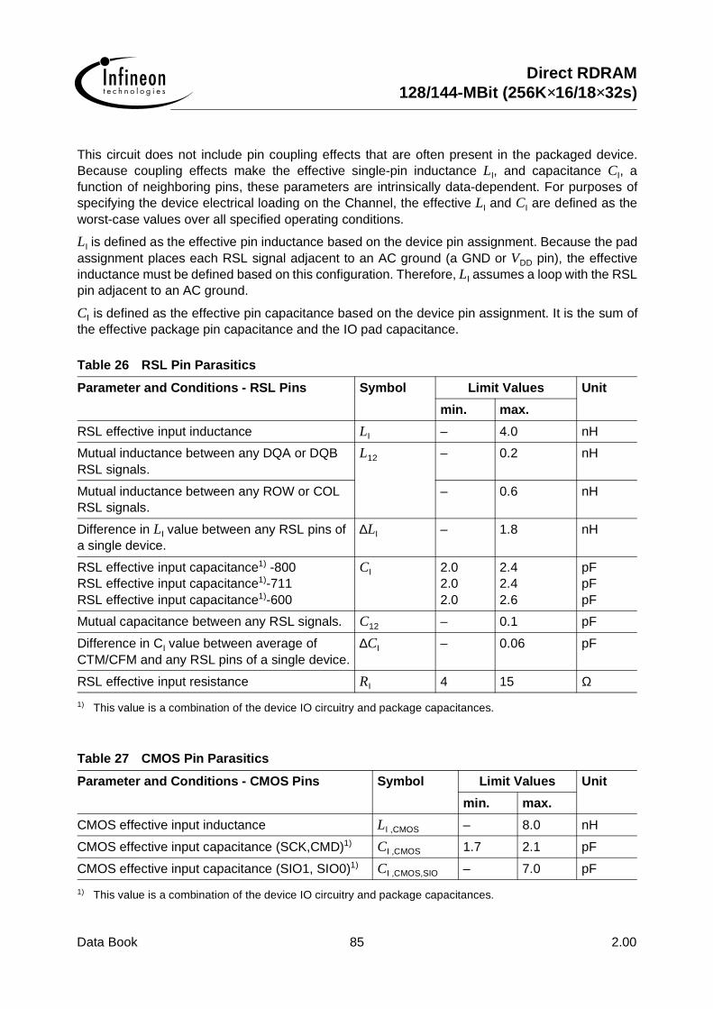
Data Book 85 2.00
Direct RDRAM128/144-MBit (256K×16/18×32s)
This circuit does not include pin coupling effects that are often present in the packaged device.Because coupling effects make the effective single-pin inductance LI, and capacitance CI, afunction of neighboring pins, these parameters are intrinsically data-dependent. For purposes ofspecifying the device electrical loading on the Channel, the effective LI and CI are defined as theworst-case values over all specified operating conditions.
LI is defined as the effective pin inductance based on the device pin assignment. Because the padassignment places each RSL signal adjacent to an AC ground (a GND or VDD pin), the effectiveinductance must be defined based on this configuration. Therefore, LI assumes a loop with the RSLpin adjacent to an AC ground.
CI is defined as the effective pin capacitance based on the device pin assignment. It is the sum ofthe effective package pin capacitance and the IO pad capacitance.
Table 26 RSL Pin Parasitics
Parameter and Conditions - RSL Pins Symbol Limit Values Unit
min. max.
RSL effective input inductance LI – 4.0 nH
Mutual inductance between any DQA or DQB RSL signals.
L12 – 0.2 nH
Mutual inductance between any ROW or COL RSL signals.
– 0.6 nH
Difference in LI value between any RSL pins of a single device.
∆LI – 1.8 nH
RSL effective input capacitance1) -800RSL effective input capacitance1)-711RSL effective input capacitance1)-600
1) This value is a combination of the device IO circuitry and package capacitances.
CI 2.02.02.0
2.42.42.6
pFpFpF
Mutual capacitance between any RSL signals. C12 – 0.1 pF
Difference in CI value between average of CTM/CFM and any RSL pins of a single device.
∆CI – 0.06 pF
RSL effective input resistance RI 4 15 Ω
Table 27 CMOS Pin Parasitics
Parameter and Conditions - CMOS Pins Symbol Limit Values Unit
min. max.
CMOS effective input inductance LI ,CMOS – 8.0 nH
CMOS effective input capacitance (SCK,CMD)1)
1) This value is a combination of the device IO circuitry and package capacitances.
CI ,CMOS 1.7 2.1 pF
CMOS effective input capacitance (SIO1, SIO0)1) CI ,CMOS,SIO – 7.0 pF

Direct RDRAM128/144-MBit (256K×16/18×32s)
Data Book 86 2.00
Center-Bonded FBGA Package
Figure 61 shows the form and dimensions of the recommended package for the center-bonded CSPdevice class.
Figure 61 Center-Bonded FBGA Package
Table 28 lists the numerical values corresponding to dimensions shown in Figure 61.
A B C D E F G H J
1
2
3
4
5
6
7
D
A
e1d E E1
8
e2
Top Bottom
Bottom
Bottom
9
10
11
2

Data Book 87 2.00
Direct RDRAM128/144-MBit (256K×16/18×32s)
Table 28 Center-Bonded FBGA Package Dimensions
Parameter Symbol Limit Values Unit
min. max.
Ball pitch (x-axis) e1 1.00 1.00 mm
Ball pitch (y-axis) e2 0.8 0.8 mm
Package body length A 10.9 11.1 mm
Package body width D 10.4 10.6 mm
Package total thickness E 0.65 1.05 mm
Ball height E1 0.18 0.35 mm
Ball diameter d 0.3 0.4 mm

Direct RDRAM128/144-MBit (256K×16/18×32s)
Data Book 88 2.00
Glossary of Terms
ACT Activate command from AV field.
activate To access a row and place in sense amp.
adjacent Two RDRAM banks which share sense amps (also called doubled banks).
ASYM CCA register field for RSL VOL/VOH.
ATTN Power state - ready for ROW/COL packets.
ATTNR Power state - transmitting Q packets.
ATTNW Power state - receiving D packets.
AV Opcode field in ROW packets.
bank A block of 2RBIT × 2CBIT storage cells in the core of the RDRAM.
BC Bank address field in COLC packet.
BBIT CNFGA register field - # bank address bits.
broadcast An operation executed by all RDRAMs.
BR Bank address field in ROW packets.
bubble Idle cycle(s) on RDRAM pins needed because of a resource constraint.
BYT CNFGB register field - 8/9 bits per byte.
BX Bank address field in COLX packet.
C Column address field in COLC packet.
CAL Calibrate (IOL) command in XOP field.
CBIT CNFGB register field - # column address bits.
CCA Control register - current control A.
CCB Control register - current control B.
CFM,CFMN Clock pins for receiving packets.
Channel ROW/COL/DQ pins and external wires.
CLRR Clear reset command from SOP field.
CMD CMOS pin for initialization/power control.
CNFGA Control register with configuration fields.
CNFGB Control register with configuration fields.
COL Pins for column-access control.
COL COLC,COLM,COLX packet on COL pins.
COLC Column operation packet on COL pins.
COLM Write mask packet on COL pins.
column Rows in a bank or activated row in sense amps have 2CBIT dualocts column storage.
command A decoded bit-combination from a field.
COLX Extended operation packet on COL pins.

Data Book 89 2.00
Direct RDRAM128/144-MBit (256K×16/18×32s)
controller A logic-device which drives the ROW/COL /DQ wires for a Channel of RDRAMs.
COP Column opcode field in COLC packet.
core The banks and sense amps of an RDRAM.
CTM,CTMN Clock pins for transmitting packets.
current control Periodic operations to update the proper IOL value of RSL output drivers.
D Write data packet on DQ pins.
DBL CNFGB register field - doubled-bank.
DC Device address field in COLC packet.
device An RDRAM on a Channel.
DEVID Control register with device address that is matched against DR, DC, and DX fields.
DM Device match for ROW packet decode.
doubled-bank RDRAM with shared sense amp.
DQ DQA and DQB pins.
DQA Pins for data byte A.
DQB Pins for data byte B.
DQS NAPX register field - PDN/NAP exit.
DR,DR4T,DR4F Device address field and packet framing fields in ROWA and ROWR packets.
dualoct 16 bytes - the smallest addressable datum.
DX Device address field in COLX packet.
field A collection of bits in a packet.
INIT Control register with initialization fields.
initialization Configuring a Channel of RDRAMs so they are ready to respond to transactions.
LSR CNFGA register field - low-power self-refresh.
M Mask opcode field (COLM/COLX packet).
MA Field in COLM packet for masking byte A.
MB Field in COLM packet for masking byte B.
MSK Mask command in M field.
MVER Control register - manufacturer ID.
NAP Power state - needs SCK/CMD wakeup.
NAPR Nap command in ROP field.
NAPRC Conditional nap command in ROP field.
NAPXA NAPX register field - NAP exit delay A.
NAPXB NAPX register field - NAP exit delay B.
NOCOP No-operation command in COP field.

Direct RDRAM128/144-MBit (256K×16/18×32s)
Data Book 90 2.00
NOROP No-operation command in ROP field.
NOXOP No-operation command in XOP field.
NSR INIT register field- NAP self-refresh.
packet A collection of bits carried on the Channel.
PDN Power state - needs SCK/CMD wakeup.
PDNR Powerdown command in ROP field.
PDNXA Control register - PDN exit delay A.
PDNXB Control register - PDN exit delay B.
pin efficiency The fraction of non-idle cycles on a pin.
PRE PREC,PRER,PREX precharge commands.
PREC Precharge command in COP field.
precharge Prepares sense amp and bank for activate.
PRER Precharge command in ROP field.
PREX Precharge command in XOP field.
PSX INIT register field - PDN/NAP exit.
PSR INIT register field - PDN self-refresh.
PVER CNFGB register field - protocol version.
Q Read data packet on DQ pins.
R Row address field of ROWA packet.
RBIT CNFGB register field - # row address bits.
RD/RDA Read (/precharge) command in COP field.
read Operation of accessing sense amp data.
receive Moving information from the Channel into the RDRAM (a serial stream is demuxed).
REFA Refresh-activate command in ROP field.
REFB Control register - next bank (self-refresh).
REFBIT CNFGA register field - ignore bank bits (for REFA and self-refresh).
REFP Refresh-precharge command in ROP field.
REFR Control register - next row for REFA.
refresh Periodic operations to restore storage cells.
retire The automatic operation that stores write buffer into sense amp after WR command.
RLX RLXC,RLXR,RLXX relax commands.
RLXC Relax command in COP field.
RLXR Relax command in ROP field.
RLXX Relax command in XOP field.
ROP Row-opcode field in ROWR packet.

Data Book 91 2.00
Direct RDRAM128/144-MBit (256K×16/18×32s)
row 2CBIT dualocts of cells (bank/sense amp).
ROW Pins for row-access control
ROW ROWA or ROWR packets on ROW pins.
ROWA Activate packet on ROW pins.
ROWR Row operation packet on ROW pins.
RQ Alternate name for ROW/COL pins.
RSL Rambus Signaling Levels.
SAM Sample (IOL) command in XOP field.
SA Serial address packet for control register transactions w/ SA address field.
SBC Serial broadcast field in SRQ.
SCK CMOS clock pin.
SD Serial data packet for control register transactions w/ SD data field.
SDEV Serial device address in SRQ packet.
SDEVID INIT register field - Serial device ID.
self-refresh Refresh mode for PDN and NAP.
sense amp Fast storage that holds copy of bank’s row.
SETF Set fast clock command from SOP field.
SETR Set reset command from SOP field.
SINT Serial interval packet for control register read/write transactions.
SIO0,SIO1 CMOS serial pins for control registers.
SOP Serial opcode field in SRQ.
SRD Serial read opcode command from SOP.
SRP INIT register field - Serial repeat bit.
SRQ Serial request packet for control register read/write transactions.
STBY Power state - ready for ROW packets.
SVER Control register - stepping version.
SWR Serial write opcode command from SOP.
TCAS TCLSCAS register field - tCAS core delay.
TCLS TCLSCAS register field - tCLS core delay.
TCLSCAS Control register - tCAS and tCLS delays.
TCYCLE Control register - tCYCLE delay.
TDAC Control register - tDAC delay.
TEST77 Control register - for test purposes.
TEST78 Control register - for test purposes.
TRDLY Control register - tRDLY delay.
transaction ROW,COL,DQ packets for memory access.

Direct RDRAM128/144-MBit (256K×16/18×32s)
Data Book 92 2.00
transmit Moving information from the RDRAM onto the Channel (parallel word is muxed).
WR/WRA Write (/precharge) command in COP field.
write Operation of modifying sense amp data.
XOP Extended opcode field in COLX packet

Direct RDRAM128/144-MBit (256K×16/18×32s)
Data Book 93 2.00