Embed Size (px)
Citation preview
DIRECTED ENERGY, INC.
PCO-7120 Laser Diode Driver Module
INSTALLATION and
OPERATION NOTES
Directed Energy, Inc. An IXYS Company 2401 Research Blvd. Suite 108 Fort Collins, CO. 80526 TEL: 970-493-1901 FAX: 970-493-1903 EMAIL: [email protected] WEB: www.directedenergy.com Doc #9100-0232 Rev 1

Doc #9100-0232 Rev 1 Directed Energy Inc. 2003 Page 1
Table of Contents Introduction ........................................................................................................2 Specifications.....................................................................................................3 Figure 2B – PCO-7120 Dimensional Drawing With Heat Spreader ...................5 Driver Interconnection And Circuit Operation.....................................................6
Laser Diode Connection..........................................................................9 Current Measurement .............................................................................11
Design Considerations.......................................................................................12 System Series Inductance.......................................................................12
Transmission Lines ............................................................................................15 Typical Output Waveforms.................................................................................18 Warranty ............................................................................................................18

Doc #9100-0232 Rev 1 Directed Energy Inc. 2003 Page 2
Introduction The PCO-7120 is a compact, economical OEM laser diode driver module designed to provide extremely fast, high current pulses to drive laser diodes in range finder, LIDAR, atmospheric communications and other applications requiring high current, nanosecond pulses. It offers variable output current from 5A to 50A, with continuously variable pulse widths from 12ns to >1µs and frequencies up to 1MHz. Mounting pads are provided to mount the laser diode directly to the driver, eliminating the need for interconnect cables or striplines. The four-hole mounting pattern accepts TO-18, TO-5, TO-52, 5.6MM, and 9MM packages, as well as other packages of similar dimensions and lead spacing, mounted perpendicular to the driver circuit board. To facilitate different packages and mounting preferences, there are two solder pads on the end of the board to accept various laser diode packages mounted on axis to the driver. Furthermore, the diode can be connected remotely from the driver using a low-impedance stripline interconnection between the mounting pads and the leads of the laser diode. A current monitor output may be viewed with an oscilloscope, providing a straight-forward means to observe the diode current waveform in real-time. The PCO-7120 driver provides high-speed performance, variable pulse width, current and frequency, a robust design, flexible mounting configurations and the ability to drive a wide range of laser diodes in a small package. These features provide the user with an economical OEM module with the flexibility to be readily designed into a wide range of products.
Doc #9100-0232 Rev 1 Directed Energy Inc. 2003 Page 3
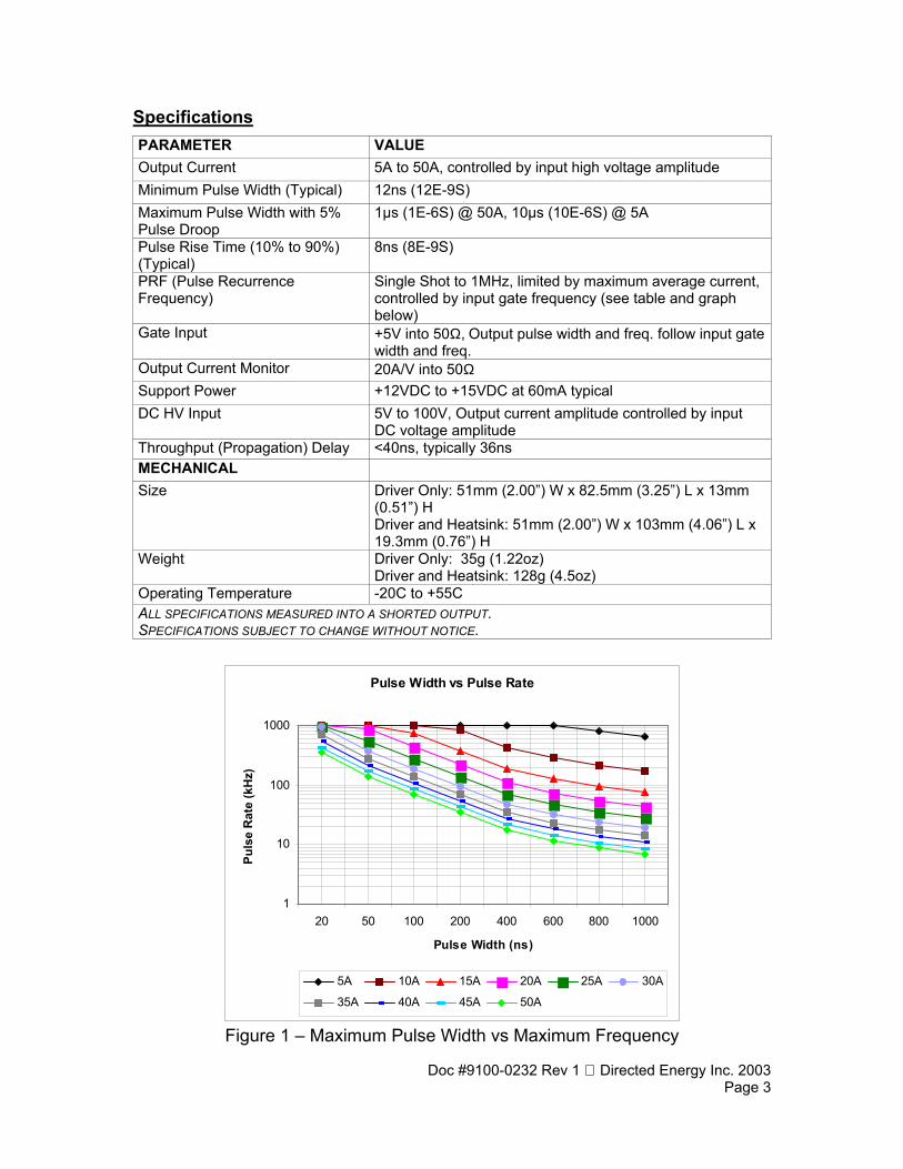
Specifications PARAMETER VALUE Output Current 5A to 50A, controlled by input high voltage amplitude Minimum Pulse Width (Typical) 12ns (12E-9S) Maximum Pulse Width with 5% Pulse Droop
1µs (1E-6S) @ 50A, 10µs (10E-6S) @ 5A
Pulse Rise Time (10% to 90%) (Typical)
8ns (8E-9S)
PRF (Pulse Recurrence Frequency)
Single Shot to 1MHz, limited by maximum average current, controlled by input gate frequency (see table and graph below)
Gate Input +5V into 50Ω, Output pulse width and freq. follow input gate width and freq.
Output Current Monitor 20A/V into 50Ω Support Power +12VDC to +15VDC at 60mA typical DC HV Input 5V to 100V, Output current amplitude controlled by input
DC voltage amplitude Throughput (Propagation) Delay <40ns, typically 36ns MECHANICAL Size Driver Only: 51mm (2.00”) W x 82.5mm (3.25”) L x 13mm
(0.51”) H Driver and Heatsink: 51mm (2.00”) W x 103mm (4.06”) L x 19.3mm (0.76”) H
Weight Driver Only: 35g (1.22oz) Driver and Heatsink: 128g (4.5oz)
Operating Temperature -20C to +55C ALL SPECIFICATIONS MEASURED INTO A SHORTED OUTPUT. SPECIFICATIONS SUBJECT TO CHANGE WITHOUT NOTICE.
Figure 1 – Maximum Pulse Width vs Maximum Frequency
Pulse Width vs Pulse Rate
1
10
100
1000
20 50 100 200 400 600 800 1000
Pulse Width (ns)
Puls
e R
ate
(kH
z)
5A 10A 15A 20A 25A 30A
35A 40A 45A 50A

Doc #9100-0232 Rev 1 Directed Energy Inc. 2003 Page 4
Output Current (A)
Maximum Duty CycleTypical DC HV Input (VDC)
5 0.65 10
10 0.17 18
15 0.075 26
20 0.045 34
25 0.028 42
30 0.019 51
40 0.011 70
50 0.007 92
Table 1 – Output Current vs Maximum Duty Cycle and Typical Input DC High Voltage
Please note that the typical DC HV input voltages in the table above are driving a shorted output. The laser diode forward voltage and the voltage required to overcome the laser diode and interconnect inductance must be taken into account in order to better approximate the actual voltage requirements. See “System Series Inductance” under the “Design Considerations” section below for additional detail.
Doc #9100-0232 Rev 1 Directed Energy Inc. 2003 Page 5
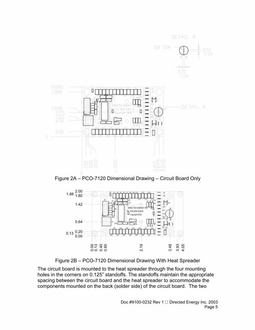
Figure 2A – PCO-7120 Dimensional Drawing – Circuit Board Only
Figure 2B – PCO-7120 Dimensional Drawing With Heat Spreader The circuit board is mounted to the heat spreader through the four mounting holes in the corners on 0.125” standoffs. The standoffs maintain the appropriate spacing between the circuit board and the heat spreader to accommodate the components mounted on the back (solder side) of the circuit board. The two
0.00
0.00
0.40
0.60
2.19
3.48
4.05
0.13 0.20
1.801.882.00
0.64
1.42
3.93
0.13
Doc #9100-0232 Rev 1 Directed Energy Inc. 2003 Page 6
socket-head screws apply pressure to the DE-Series MOSFET (mounted on the solder side), keeping it in compression against the heat spreader.
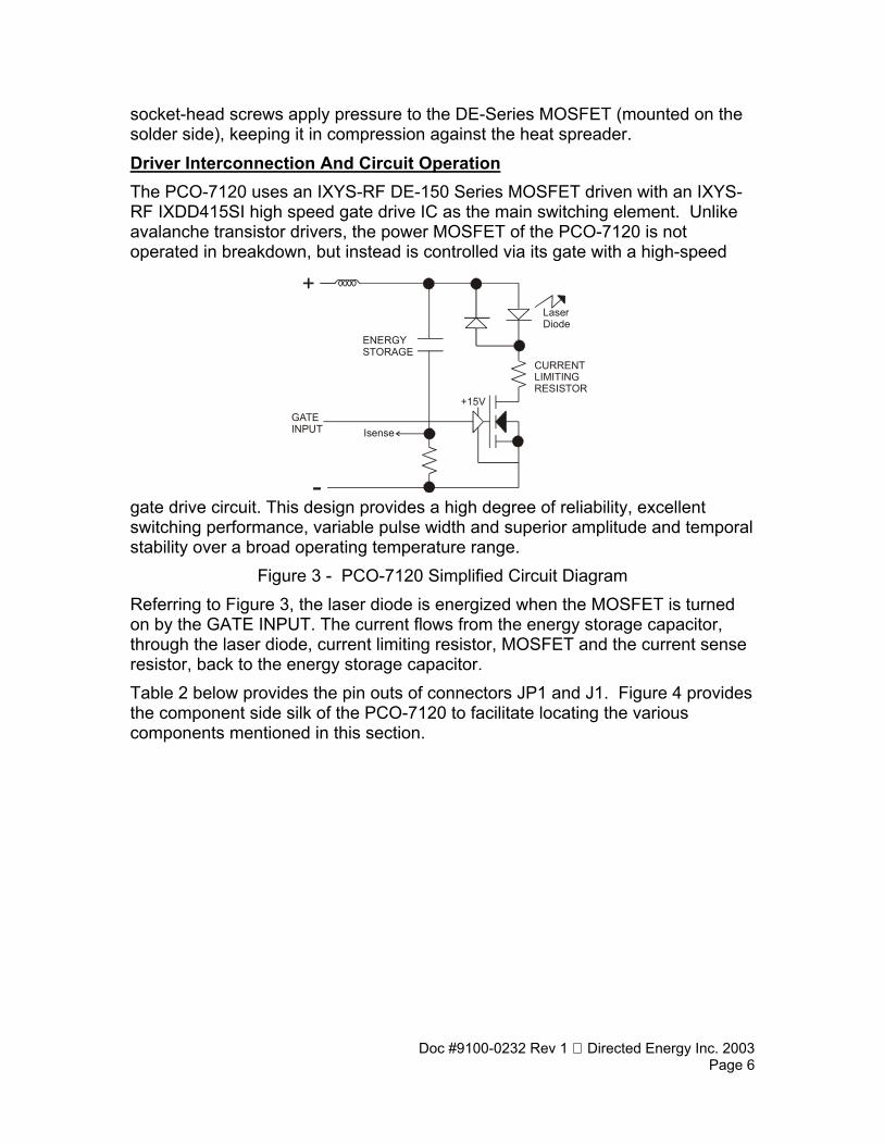
Driver Interconnection And Circuit Operation The PCO-7120 uses an IXYS-RF DE-150 Series MOSFET driven with an IXYS-RF IXDD415SI high speed gate drive IC as the main switching element. Unlike avalanche transistor drivers, the power MOSFET of the PCO-7120 is not operated in breakdown, but instead is controlled via its gate with a high-speed
gate drive circuit. This design provides a high degree of reliability, excellent switching performance, variable pulse width and superior amplitude and temporal stability over a broad operating temperature range.
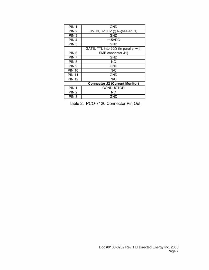
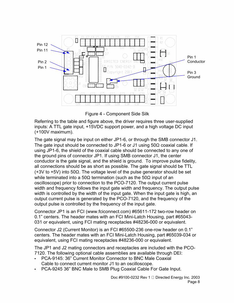
Figure 3 - PCO-7120 Simplified Circuit Diagram Referring to Figure 3, the laser diode is energized when the MOSFET is turned on by the GATE INPUT. The current flows from the energy storage capacitor, through the laser diode, current limiting resistor, MOSFET and the current sense resistor, back to the energy storage capacitor. Table 2 below provides the pin outs of connectors JP1 and J1. Figure 4 provides the component side silk of the PCO-7120 to facilitate locating the various components mentioned in this section.
+15V
+
-
GATEINPUT Isense
LaserDiode
ENERGYSTORAGE
CURRENTLIMITINGRESISTOR
Doc #9100-0232 Rev 1 Directed Energy Inc. 2003 Page 7
PIN 1 GNDPIN 2 HV IN, 0-100V @ IPS(see eq. 1)PIN 3 GNDPIN 4 +15VDCPIN 5 GND
PIN 6GATE, TTL into 50Ω (In parallel with
SMB connector J1)PIN 7 GNDPIN 8 NCPIN 9 GNDPIN 10 N/CPIN 11 GNDPIN 12 N/C
Connector J2 (Current Monitor)PIN 1 CONDUCTORPIN 2 NCPIN 3 GND Table 2. PCO-7120 Connector Pin Out
Doc #9100-0232 Rev 1 Directed Energy Inc. 2003 Page 8
Figure 4 - Component Side Silk Referring to the table and figure above, the driver requires three user-supplied inputs: A TTL gate input, +15VDC support power, and a high voltage DC input (+100V maximum). The gate signal may be input on either JP1-6, or through the SMB connector J1. The gate input should be connected to JP1-6 or J1 using 50Ω coaxial cable. If using JP1-6, the shield of the coaxial cable should be connected to any one of the ground pins of connector JP1. If using SMB connector J1, the center conductor is the gate signal, and the shield is ground. To improve pulse fidelity, all connections should be as short as possible. The gate signal should be TTL (+3V to +5V) into 50Ω. The voltage level of the pulse generator should be set while terminated into a 50Ω termination (such as the 50Ω input of an oscilloscope) prior to connection to the PCO-7120. The output current pulse width and frequency follows the input gate width and frequency. The output pulse width is controlled by the width of the input gate. When the input gate is high, an output current pulse is generated by the PCO-7120, and the frequency of the output pulse is controlled by the frequency of the input gate. Connector JP1 is an FCI (www.fciconnect.com) #65611-172 two-row header on 0.1” centers. The header mates with an FCI Mini-Latch Housing, part #65043-031 or equivalent, using FCI mating receptacles #48236-000 or equivalent. Connector J2 (Current Monitor) is an FCI #65500-236 one-row header on 0.1” centers. The header mates with an FCI Mini-Latch Housing, part #65039-034 or equivalent, using FCI mating receptacles #48236-000 or equivalent. The JP1 and J2 mating connectors and receptacles are included with the PCO-7120. The following optional cable assemblies are available through DEI: • PCA-9145: 36” Current Monitor Connector to BNC Male Coaxial
Cable to connect current monitor J1 to an oscilloscope. • PCA-9245 36” BNC Male to SMB Plug Coaxial Cable For Gate Input.
Pin 1
Pin 1 Conductor
Pin 3 Ground
Pin 2
Pin 11 Pin 12
Doc #9100-0232 Rev 1 Directed Energy Inc. 2003 Page 9
The output current depends upon the available charge of the driver’s energy storage network. This charge is directly proportional to the voltage supplied by the high voltage DC power supply. Therefore the output current amplitude of the PCO-7120 is controlled by varying the input high voltage amplitude. The DC power supply charges the PCO-7120’s on-board energy storage capacitors. Therefore the high voltage DC power supply needs to provide the maximum AVERAGE current drawn by the driver and diode, not the PEAK current. The maximum average power that the high voltage supply must provide is determined by the peak output current and duty cycle required for the user’s application. This power can be approximated by the formula:
DCIVV PULSESUPPLYPOWER ××=
where: VSUPPLY is the voltage required of the high voltage DC power supply for a given pulse output current (from Table 1 above, also see “System Series Inductance” under the “Design Considerations” section below); IPULSE is the output pulse current; DC is the duty cycle (the ratio of pulse ON time to pulse OFF time, calculated using the formula pulse width x frequency) High speed clamp diodes are incorporated into the output network to protect the laser diode against reverse voltage conditions. The driver is supplied mounted on a 1/4” aluminum heat spreader to provide the cooling needed for the switching transistor, and to simplify mounting or installation of the driver. The heat spreader temperature should be maintained below 55ºC. If the heat spreader temperature exceeds 55ºC, additional cooling should be provided either by forced air cooling across the driver and heat spreader, or by mounting the heat spreader to a heat sink or cold plate using the mounting holes provided.
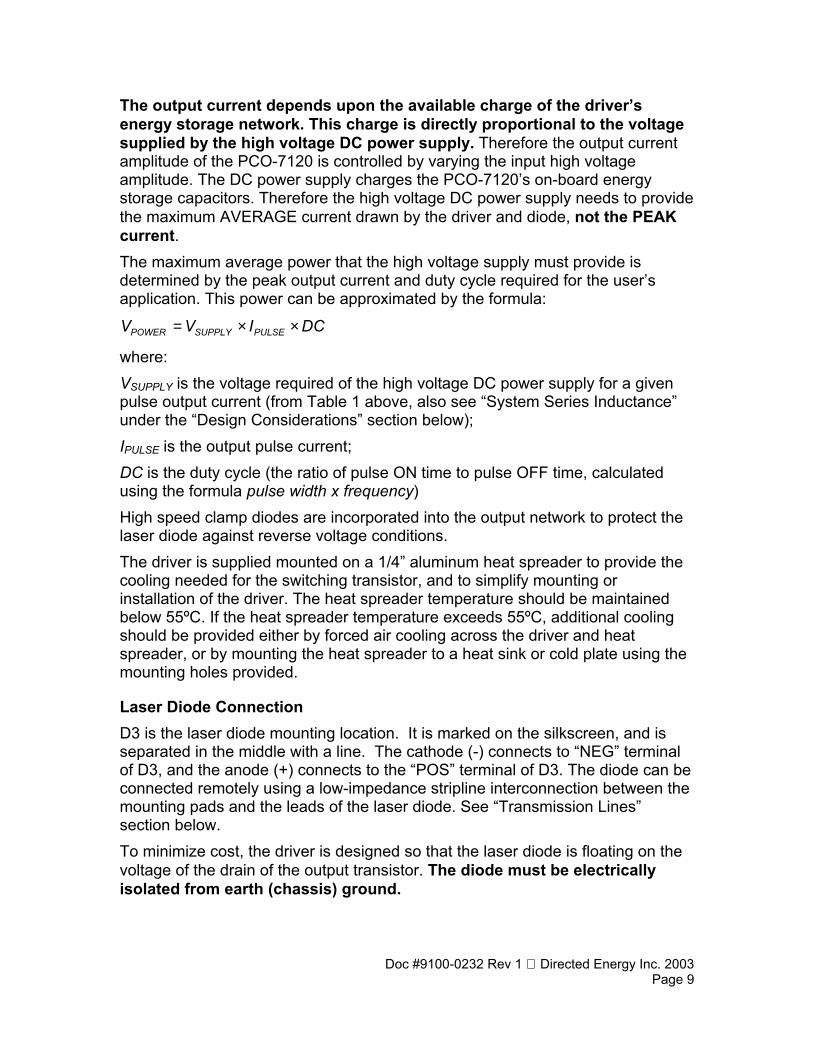
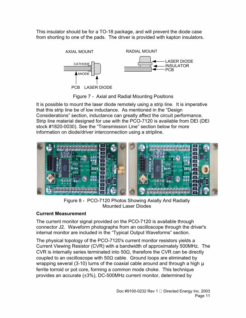
Laser Diode Connection D3 is the laser diode mounting location. It is marked on the silkscreen, and is separated in the middle with a line. The cathode (-) connects to “NEG” terminal of D3, and the anode (+) connects to the “POS” terminal of D3. The diode can be connected remotely using a low-impedance stripline interconnection between the mounting pads and the leads of the laser diode. See “Transmission Lines” section below. To minimize cost, the driver is designed so that the laser diode is floating on the voltage of the drain of the output transistor. The diode must be electrically isolated from earth (chassis) ground.
Doc #9100-0232 Rev 1 Directed Energy Inc. 2003 Page 10
Figure 5 - Cathode and Anode Pads on the PCB
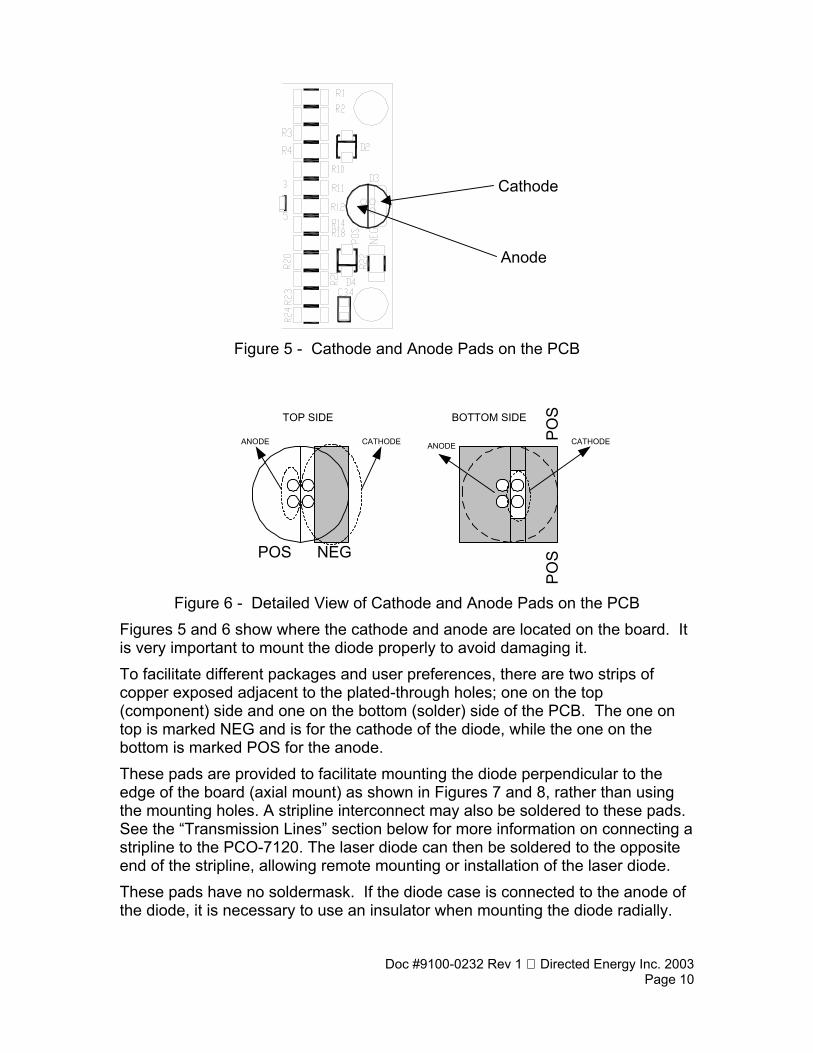
Figure 6 - Detailed View of Cathode and Anode Pads on the PCB Figures 5 and 6 show where the cathode and anode are located on the board. It is very important to mount the diode properly to avoid damaging it. To facilitate different packages and user preferences, there are two strips of copper exposed adjacent to the plated-through holes; one on the top (component) side and one on the bottom (solder) side of the PCB. The one on top is marked NEG and is for the cathode of the diode, while the one on the bottom is marked POS for the anode. These pads are provided to facilitate mounting the diode perpendicular to the edge of the board (axial mount) as shown in Figures 7 and 8, rather than using the mounting holes. A stripline interconnect may also be soldered to these pads. See the “Transmission Lines” section below for more information on connecting a stripline to the PCO-7120. The laser diode can then be soldered to the opposite end of the stripline, allowing remote mounting or installation of the laser diode. These pads have no soldermask. If the diode case is connected to the anode of the diode, it is necessary to use an insulator when mounting the diode radially.
NEG
ANODE CATHODE
TOP SIDE
ANODE CATHODE
BOTTOM SIDE
POSP
OS
POS
Cathode
Anode
Doc #9100-0232 Rev 1 Directed Energy Inc. 2003 Page 11
This insulator should be for a TO-18 package, and will prevent the diode case from shorting to one of the pads. The driver is provided with kapton insulators.
Figure 7 - Axial and Radial Mounting Positions It is possible to mount the laser diode remotely using a strip line. It is imperative that this strip line be of low inductance. As mentioned in the “Design Considerations” section, inductance can greatly affect the circuit performance. Strip line material designed for use with the PCO-7120 is available from DEI (DEI stock #1820-0030). See the “Transmission Line” section below for more information on diode/driver interconnection using a stripline.
Current Measurement The current monitor signal provided on the PCO-7120 is available through connector J2. Waveform photographs from an oscilloscope through the driver's internal monitor are included in the “Typical Output Waveforms” section. The physical topology of the PCO-7120's current monitor resistors yields a Current Viewing Resistor (CVR) with a bandwidth of approximately 500MHz. The CVR is internally series terminated into 50Ω, therefore the CVR can be directly coupled to an oscilloscope with 50Ω cable. Ground loops are eliminated by wrapping several (3-10) turns of the coaxial cable around and through a high µ ferrite torroid or pot core, forming a common mode choke. This technique provides an accurate (±3%), DC-500MHz current monitor, determined by
LASER DIODEINSULATORPCB
RADIAL MOUNTAXIAL MOUNT
LASER DIODEPCB
CATHODE
ANODE
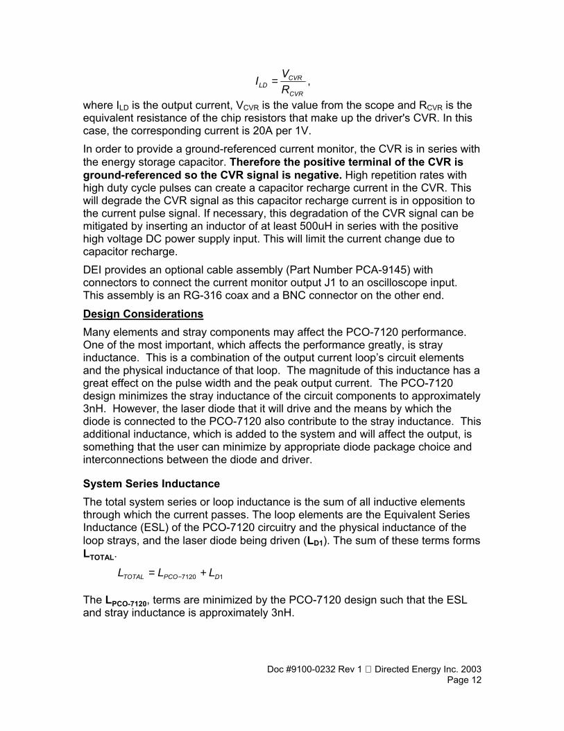
Figure 8 - PCO-7120 Photos Showing Axially And Radially Mounted Laser Diodes
Doc #9100-0232 Rev 1 Directed Energy Inc. 2003 Page 12
CVR
CVRLD R
VI = ,
where ILD is the output current, VCVR is the value from the scope and RCVR is the equivalent resistance of the chip resistors that make up the driver's CVR. In this case, the corresponding current is 20A per 1V. In order to provide a ground-referenced current monitor, the CVR is in series with the energy storage capacitor. Therefore the positive terminal of the CVR is ground-referenced so the CVR signal is negative. High repetition rates with high duty cycle pulses can create a capacitor recharge current in the CVR. This will degrade the CVR signal as this capacitor recharge current is in opposition to the current pulse signal. If necessary, this degradation of the CVR signal can be mitigated by inserting an inductor of at least 500uH in series with the positive high voltage DC power supply input. This will limit the current change due to capacitor recharge. DEI provides an optional cable assembly (Part Number PCA-9145) with connectors to connect the current monitor output J1 to an oscilloscope input. This assembly is an RG-316 coax and a BNC connector on the other end.
Design Considerations Many elements and stray components may affect the PCO-7120 performance. One of the most important, which affects the performance greatly, is stray inductance. This is a combination of the output current loop’s circuit elements and the physical inductance of that loop. The magnitude of this inductance has a great effect on the pulse width and the peak output current. The PCO-7120 design minimizes the stray inductance of the circuit components to approximately 3nH. However, the laser diode that it will drive and the means by which the diode is connected to the PCO-7120 also contribute to the stray inductance. This additional inductance, which is added to the system and will affect the output, is something that the user can minimize by appropriate diode package choice and interconnections between the diode and driver.
System Series Inductance The total system series or loop inductance is the sum of all inductive elements through which the current passes. The loop elements are the Equivalent Series Inductance (ESL) of the PCO-7120 circuitry and the physical inductance of the loop strays, and the laser diode being driven (LD1). The sum of these terms forms LTOTAL.
17120 DPCOTOTAL LLL += −
The LPCO-7120, terms are minimized by the PCO-7120 design such that the ESL and stray inductance is approximately 3nH.
Doc #9100-0232 Rev 1 Directed Energy Inc. 2003 Page 13
The magnitude of the LTOTAL term will affect pulse rise time, minimum pulse width and circuit impedance. The effect of LTOTAL on the operating voltage and the peak current is shown by the following relationships:
V L didtL TOTALTOTAL
= where di is the peak current and dt is the 100% rise
time. and:
IV V
RPEAKSUPPLY L
S
TOTAL≅−
Where RS is the system series resistance, about 1.6 Ohms.
Rearranging terms we have; V I R VSUPPLY PEAK S LTOTAL
≅ +
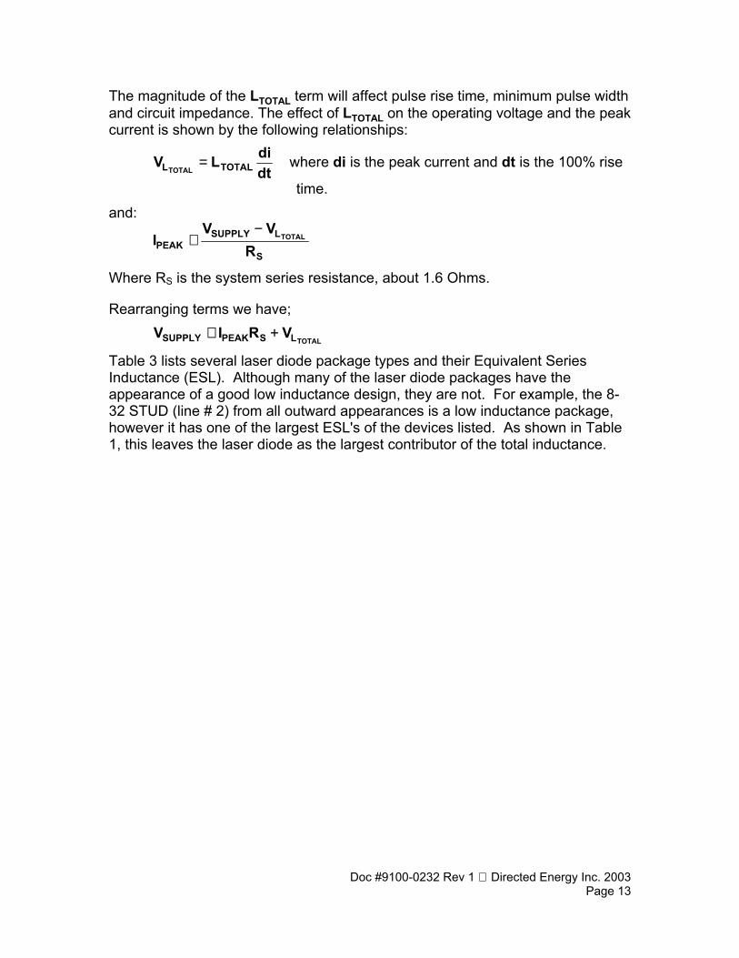
Table 3 lists several laser diode package types and their Equivalent Series Inductance (ESL). Although many of the laser diode packages have the appearance of a good low inductance design, they are not. For example, the 8-32 STUD (line # 2) from all outward appearances is a low inductance package, however it has one of the largest ESL's of the devices listed. As shown in Table 1, this leaves the laser diode as the largest contributor of the total inductance.
Doc #9100-0232 Rev 1 Directed Energy Inc. 2003 Page 14
# PACKAGE STYLE PACKAGE INDUCTANCE
1 Dip 14 Leads out top
15.7nH
2 8-32 STUD 12nH
3 10-32 STUD 11nH
4 TO-5 (2 lead) 9.6nH
5 TO-52 6.8nH
6
Long Horn 14 Pin
6.4nH
7 CD9mm 5.2nH
8 .200.060 Hight
.014 lead diameterKOVAR Gold Plate
5.0nH
9 .200.060 Hight
.014 lead diameterCOPPER
3.6nH
10 .078.039 Hight
.014 lead diameterCOPPER
1.56nH
Table 3 Package Style Vs Package Inductance
The ESL of the PCO-7120 are minimized by the PCO-7120 design to about 3nH. As shown in Table 3, this leaves the laser diode as the largest contributor to the total inductance. To explore this let us look at the voltage requirement for a PCO-7120 using an 8-32 stud laser diode package. Let: di=40A dt=8ns 100% rise time L= LPCO-7120+L8-32STUD = 15nH Then:
dtdiLV = =
nsAnH
84015 = 75V
This tells us that, for 40A to flow in 8ns, the loop inductance will require approximately a 75V pulse. However this does not account for resistive losses in the circuit. This loss will require even more voltage. From the discussion above, the summation is then:
dtdiLVIRV TOTALDIODELASERPEAKSply ++= −sup
8ns40AnH154V(40A)6.1Vsupply ++Ω= = 143V
From this we see that we will need ≈ 143V to drive our laser diode to 40A in 8ns.
Doc #9100-0232 Rev 1 Directed Energy Inc. 2003 Page 15
Since the PCO-7120 has a maximum input voltage of 100V, it will not be capable of driving this diode to 40A with an 8ns pulse rise time. Therefore either the user must accept a slower rise time, or a laser diode package with lower inductance must be chosen. Substituting a CD9mm laser diode, with an ESL of 5.2nH in place of an 8-32 stud mount laser diode with an ESL of 12nH:
8ns40AnH2.84V(40A)6.1VSUPPLY ++Ω≅ = 109V
Therefore substituting a CD9mm package in place of the 8-32 stud package will allow the driver to come very close to achieving 40A with an 8ns rise time.
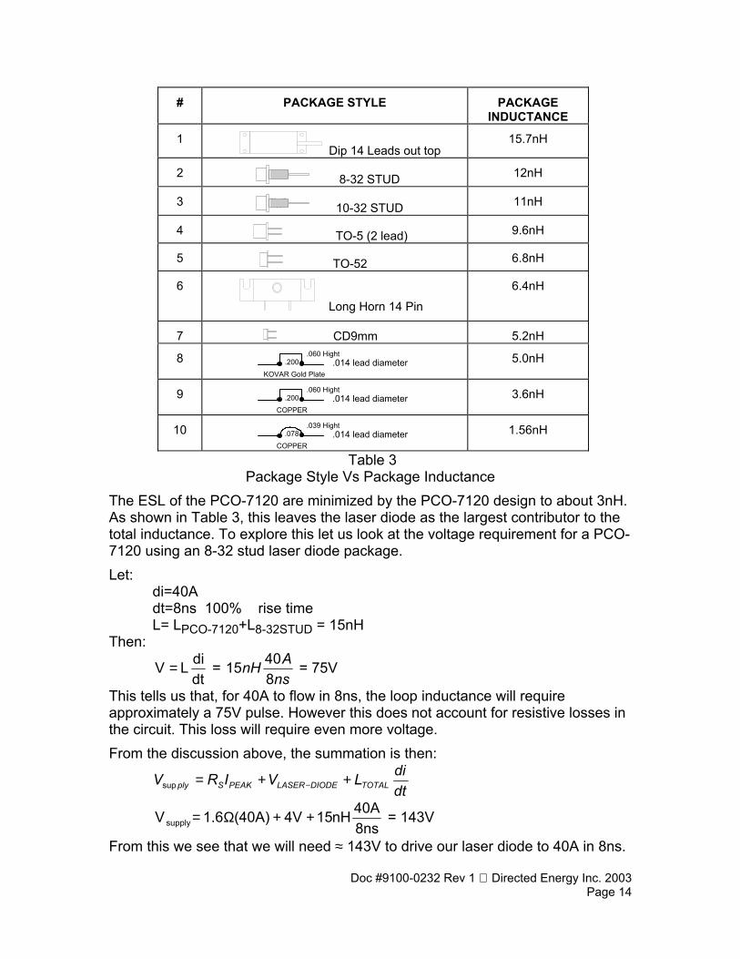
Transmission Lines The PCO-7120 circuit is a matched impedance configuration such that ZD ≈ ZL, where ZD is the output impedance of the PCO-7120, and ZL is the impedance of the laser diode.
At the top of Figure 9 we see a Driver (ZD) connected to a load (ZL). In this configuration the two elements are virtually integrated. ZD ≈ ZL, maximum power is transferred with minimum loss, and pulse fidelity is preserved. This then represents the ideal topology, and represents the PCO-7120 when the laser diode is mounted directly onto the circuit board. However this is not always an option for many circuit configurations. In some cases it is necessary to locate the laser diode at some distance from the driver. This is illustrated in the lower half of Figure 9. The maximum distance will be determined by the line losses that can be tolerated given the system requirements. The transmission lines used for this type of application are substantially different from the standard 50Ω coaxial cable. System requirements are often such that the line impedance must be between 0.2Ω and 2Ω. The mechanical system constraints could require an extremely flexible low mass construction. The transmission line topologies that best address these requirements are the micro stripline or the stripline types constructed with copper foils and polymer films.
Z Driver Z Line Z Load
Micro Stripline
Z Driver Z Load
Figure 9 System Topologies
Doc #9100-0232 Rev 1 Directed Energy Inc. 2003 Page 16
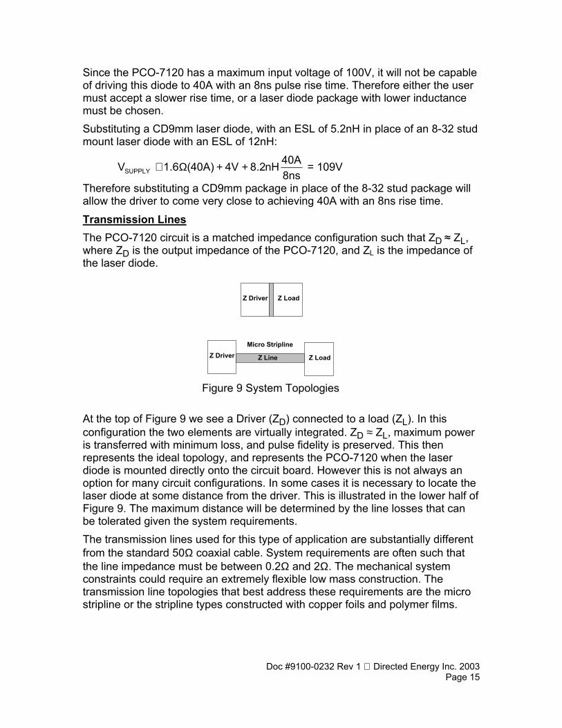
Figure 10 is a Micro Stripline constructed of copper and Kapton tape, similar to the DEI part number 1820-0030 stripline. This type of mechanical construction produces a transmission line that is easily fabricated at very low impedance levels. It is strong, light, extremely flexible and low cost.
The characteristic impedance in given by the equation below. By adjusting h and/or changing the width W, we can set the impedance at the desired value (5). The ground foil should be approximately 10h on either side to minimize edge effects (5).
For: Wh
> 1 and ZD ≈ ZL ≈ RS
Then: ZEWh
E0
120
=
π
(5)
Given:
EE ≈ 3.5 (for Kapton) h = .002in. = 2E-3in. W = .195in = 1.95E-1in.
Then: Z0
3771 8797 5
20197 5
2 06 2= = = ≈.. .
. Ω Ω
The DEI 1820-0030 stripline is connected to the PCO-7120 by soldering the end of the stripline to the anode and cathode pads on the end of the circuit board. The laser diode may be soldered to the end of the stripline as illustrated below, or a diode mounting board can be developed with mounting holes to accommodate the laser diode and pads to which the stripline can be soldered. To solder the stripline to the driver, strip back approximately 1 centimeter of the kapton (polyamide) insulation, exposing the copper conductors. Solder the cathode (negative) connection to the pad on the top of the circuit board, and the anode (positive) connection to the pad on the bottom (solder) side of the circuit board. The circuit board must be removed from the heat spreader in order to solder the bottom connection. To remove the board, remove the four screws in the corners of the board, and the two socket-head screws located near the middle of the board. (The socket-head screws apply pressure to the DE-Series
W
h
Adhesive
.002in.CopperFoil
10 h
Apx. .0005in.
.002in.Kapton3 places
Figure 10 Micro Stripline Transmission Line
Doc #9100-0232 Rev 1 Directed Energy Inc. 2003 Page 17
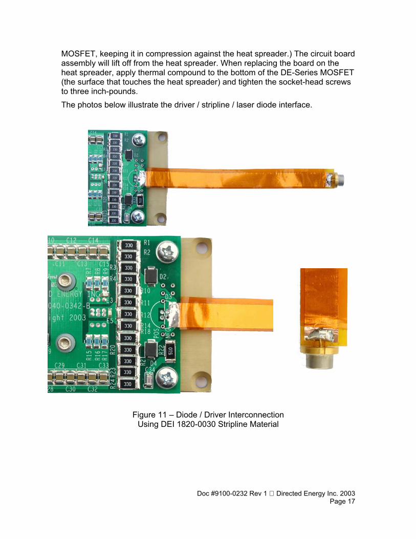
MOSFET, keeping it in compression against the heat spreader.) The circuit board assembly will lift off from the heat spreader. When replacing the board on the heat spreader, apply thermal compound to the bottom of the DE-Series MOSFET (the surface that touches the heat spreader) and tighten the socket-head screws to three inch-pounds. The photos below illustrate the driver / stripline / laser diode interface.
Figure 11 – Diode / Driver Interconnection Using DEI 1820-0030 Stripline Material

Doc #9100-0232 Rev 1 Directed Energy Inc. 2003 Page 18
Typical Output Waveforms Below are typical output waveforms from the PCO-7120. All waveforms are shown driving a short in place of the laser diode.
Warranty There are no warranties, express or implied, including any implied warranty of fitness for a particular purpose nor any IMPLIED WARRANTY OF MERCHANTIBILITY made by Directed Energy, Inc. (DEI) except as follows: DEI warrants equipment manufactured by it to be free from defects in materials and/or workmanship under conditions of normal use for a period of one year from the date of shipment to the purchaser. DEI will repair or replace, at DEI's option, any product manufactured by it which is shown to be defective or fails to perform within specifications within one year from the date of shipment to the purchaser. OEM, modified and custom items of equipment are similarly warranted, for a period of ninety (90) days from date of shipment to the purchaser. Equipment claimed to be defective must be returned, transportation prepaid, to DEI's factory in Fort Collins, Colorado within the warranty period. Returns must be preauthorized by contact with DEI's customer service department. Written documentation of such preauthorization shall be included with the returned item. At DEI's discretion, DEI may elect to repair or replace the equipment claimed to be defective or refund the original purchase price, plus taxes and transportation charges incurred by the purchaser. This Warranty shall not apply to any product that has been: 1. Repaired, worked on, or altered by persons unauthorized by DEI; 2. Subjected to misuse, neglect, or damage by others; or 3. Connected, installed, adjusted, or used in a manner not authorized in the
instructions or specifications furnished by DEI. This warranty is the purchaser's sole remedy for claimed defects in the equipment sold or manufactured by DEI. DEI's liability to the purchaser is limited to the repair or replacement of the claimed defective equipment or, at DEI's
12ns Pulse Width, 50A Output 1us Pulse Width, 50A Output 200ns Pulse Width, 10A Output

Doc #9100-0232 Rev 1 Directed Energy Inc. 2003 Page 19
option, refund of the purchase price, taxes and transportation charges incurred by the purchaser. DEI will not be responsible for or liable to the purchaser for consequential losses or damages asserted to be attributable to a claimed defect in the equipment provided. Changes made by DEI in the design or manufacture of similar equipment which are effected subsequent to the date of shipment of the warranted equipment to the purchaser are reflective of DEI's program of constant product development and improvement and shall not be construed as an acknowledgement of deficiency in the product shipped to purchaser. DEI will be under no obligation to make any changes to product previously shipped.