Embed Size (px)
Citation preview
Discretely tunable III-V/SOI SG-DFB laserS. Dhoore,1,2 G. Roelkens,1,2 and G. Morthier1,2
1 Photonics Research Group, INTEC-department, Ghent University-IMEC, Belgium2 Center for Nano- and Biophotonics (NB-Photonics), Ghent University, Belgium
Discrete wavelength tuning with a heterogeneously integrated III-V/SOI sampled gratingdistributed feedback (SG-DFB) laser is demonstrated. The laser device is tunable over awavelength range larger than 55 nm in wavelength steps of 5 nm and only employs twoinjection currents. A maximum fiber-coupled output power of -1.8 dBm is obtained aswell as a high side mode suppression of more than 33 dB for all wavelength channels.The demonstrated laser is expected to find application in future flexible optical networkarchitectures.
IntroductionWith the increasing demand for bandwidth, widely tunable laser diodes are expected toplay an increasingly important role as light sources in future advanced data center andmetro networks. Additional functionality in flexible optical network architectures canfor instance be achieved through fast bandwidth relocation by dynamically increasing thenumber of links between hot spots in the network [1]. Optical switches or cross connectsthat can be used for this purpose require very fast and widely tunable laser diodes withhigh power efficiency [2].Recently, significant research has been done in the area of III-V/SOI laser diodes, inwhich laser structures are realised through integration of III-V epitaxy on the SOI plat-form through direct or adhesive wafer bonding techniques [3]. In this way the laser de-vices can be co-integrated with silicon passive waveguide circuits, high-speed siliconmodulators and germanium photodetectors. As opposed to traditional InP-lasers, mem-brane III-V/SOI lasers allow the realization of gratings with a high coupling coefficientand strong optical confinement in the gain material.Different III-V/SOI tunable lasers have been demonstrated already. These laser structurestypically make use of one or more ring resonator filters with heaters that allow to ther-mally tune the lasing wavelength [4, 5]. An alternative laser structure that consists of 2sampled grating DBR mirrors, a gain and a phase section, has been used to demonstrateover 13 nm wavelength tuning [6].In this paper, we present the experimental demonstration of a novel widely tunable sam-pled grating distributed feedback (SG-DFB) laser integrated on SOI. The laser is tunableover a wavelength range larger than 55 nm in discrete wavelength steps of 5 nm, with allwavelength channels having a side mode suppression ratio (SMSR) of more than 33 dB.
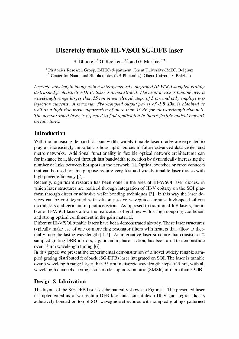
Design & fabricationThe layout of the SG-DFB laser is schematically shown in Figure 1. The presented laseris implemented as a two-section DFB laser and constitutes a III-V gain region that isadhesively bonded on top of SOI waveguide structures with sampled gratings patterned
z
x
y
Si output
III-V membrane
FrontSG
Back
SG
DVS-BCB
Figure 1: Layout of the SG-DFB laser. The front and back SG have a slightly differentsampling period to exploit the Vernier effect for wide wavelength tuning.
Pt for FIB cut
Ti/Au
p++-InGaAs
p-InP
MQWs n-InPn-InP
DVS-BCB
Si3N4 Si3N4
DVS-BCB
DVS-BCB
Si
BOX
Si substrate
z
y
(b)
Ti/Au
p++-InGaAs
p-InP
MQWs
n-InP
DVS-BCB
SiBOX
z
x
(a)
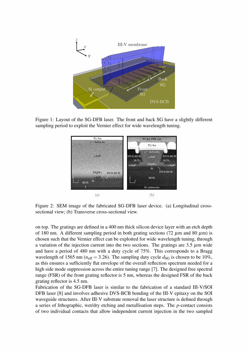
Figure 2: SEM image of the fabricated SG-DFB laser device. (a) Longitudinal cross-sectional view; (b) Transverse cross-sectional view.
on top. The gratings are defined in a 400 nm thick silicon device layer with an etch depthof 180 nm. A different sampling period in both grating sections (72 µm and 80 µm) ischosen such that the Vernier effect can be exploited for wide wavelength tuning, througha variation of the injection current into the two sections. The gratings are 3.5 µm wideand have a period of 480 nm with a duty cycle of 75%. This corresponds to a Braggwavelength of 1565 nm (neff = 3.26). The sampling duty cycle dSG is chosen to be 10%,as this ensures a sufficiently flat envelope of the overall reflection spectrum needed for ahigh side mode suppression across the entire tuning range [7]. The designed free spectralrange (FSR) of the front grating reflector is 5 nm, whereas the designed FSR of the backgrating reflector is 4.5 nm.Fabrication of the SG-DFB laser is similar to the fabrication of a standard III-V/SOIDFB laser [8] and involves adhesive DVS-BCB bonding of the III-V epitaxy on the SOIwaveguide structures. After III-V substrate removal the laser structure is defined througha series of lithographic, wet/dry etching and metallisation steps. The p-contact consistsof two individual contacts that allow independent current injection in the two sampled
0 25 50 75 100 125 150 175 2000
0.1
0.2
0.3
0.4
0.5
0.6
0.7
Ifront (mA)
OutputPow
er(m
W) Iback 100 mA
Iback 150 mAIback 200 mAIback 250 mA
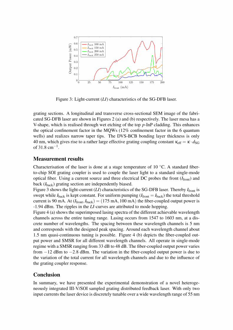
Figure 3: Light-current (LI) characteristics of the SG-DFB laser.
grating sections. A longitudinal and transverse cross-sectional SEM image of the fabri-cated SG-DFB laser are shown in Figures 2 (a) and (b) respectively. The laser mesa has aV-shape, which is realised through wet etching of the top p-InP cladding. This enhancesthe optical confinement factor in the MQWs (12% confinement factor in the 6 quantumwells) and realizes narrow taper tips. The DVS-BCB bonding layer thickness is only40 nm, which gives rise to a rather large effective grating coupling constant κeff = κ ·dSGof 31.8 cm−1.
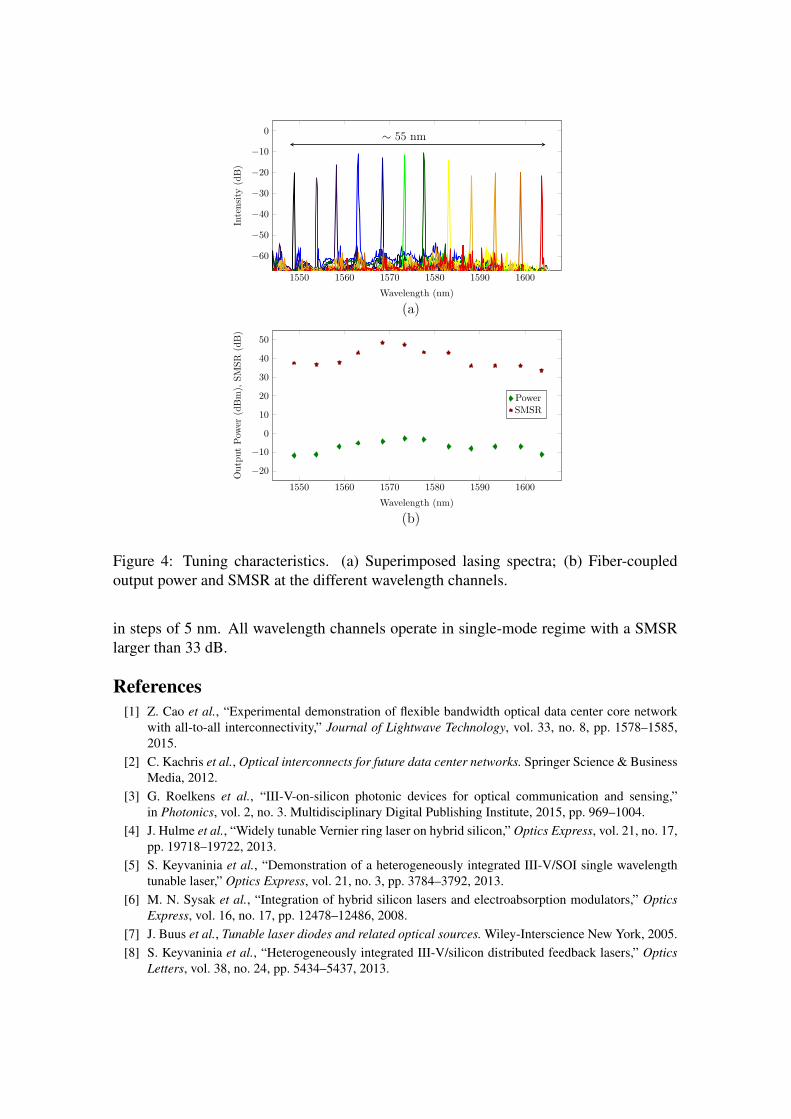
Measurement resultsCharacterisation of the laser is done at a stage temperature of 10 ◦C. A standard fiber-to-chip SOI grating coupler is used to couple the laser light to a standard single-modeoptical fiber. Using a current source and three electrical DC probes the front (Ifront) andback (Iback) grating section are independently biased.Figure 3 shows the light-current (LI) characteristics of the SG-DFB laser. Thereby Ifront isswept while Iback is kept constant. For uniform pumping (Ifront = Iback) the total thresholdcurrent is 90 mA. At (Ifront, Iback) = (175 mA,100 mA) the fiber-coupled output power is-1.94 dBm. The ripples in the LI-curves are attributed to mode hopping.Figure 4 (a) shows the superimposed lasing spectra of the different achievable wavelengthchannels across the entire tuning range. Lasing occurs from 1547 to 1603 nm, at a dis-crete number of wavelengths. The spacing between these wavelength channels is 5 nmand corresponds with the designed peak spacing. Around each wavelength channel about1.5 nm quasi-continuous tuning is possible. Figure 4 (b) depicts the fiber-coupled out-put power and SMSR for all different wavelength channels. All operate in single-moderegime with a SMSR ranging from 33 dB to 48 dB. The fiber-coupled output power variesfrom −12 dBm to −2.8 dBm. The variation in the fiber-coupled output power is due tothe variation of the total current for all wavelength channels and due to the influence ofthe grating coupler response.
ConclusionIn summary, we have presented the experimental demonstration of a novel heteroge-neously integrated III-V/SOI sampled grating distributed feedback laser. With only twoinput currents the laser device is discretely tunable over a wide wavelength range of 55 nm
∼ 55 nm
1550 1560 1570 1580 1590 1600
−60
−50
−40
−30
−20
−10
0
Wavelength (nm)
Intensity
(dB)
(a)
1550 1560 1570 1580 1590 1600
−20
−10
0
10
20
30
40
50
Wavelength (nm)
OutputPow
er(dBm),
SMSR
(dB)
PowerSMSR
(b)
Figure 4: Tuning characteristics. (a) Superimposed lasing spectra; (b) Fiber-coupledoutput power and SMSR at the different wavelength channels.
in steps of 5 nm. All wavelength channels operate in single-mode regime with a SMSRlarger than 33 dB.
References[1] Z. Cao et al., “Experimental demonstration of flexible bandwidth optical data center core network
with all-to-all interconnectivity,” Journal of Lightwave Technology, vol. 33, no. 8, pp. 1578–1585,2015.
[2] C. Kachris et al., Optical interconnects for future data center networks. Springer Science & BusinessMedia, 2012.
[3] G. Roelkens et al., “III-V-on-silicon photonic devices for optical communication and sensing,”in Photonics, vol. 2, no. 3. Multidisciplinary Digital Publishing Institute, 2015, pp. 969–1004.
[4] J. Hulme et al., “Widely tunable Vernier ring laser on hybrid silicon,” Optics Express, vol. 21, no. 17,pp. 19718–19722, 2013.
[5] S. Keyvaninia et al., “Demonstration of a heterogeneously integrated III-V/SOI single wavelengthtunable laser,” Optics Express, vol. 21, no. 3, pp. 3784–3792, 2013.
[6] M. N. Sysak et al., “Integration of hybrid silicon lasers and electroabsorption modulators,” OpticsExpress, vol. 16, no. 17, pp. 12478–12486, 2008.
[7] J. Buus et al., Tunable laser diodes and related optical sources. Wiley-Interscience New York, 2005.[8] S. Keyvaninia et al., “Heterogeneously integrated III-V/silicon distributed feedback lasers,” Optics
Letters, vol. 38, no. 24, pp. 5434–5437, 2013.