Embed Size (px)
Citation preview
Distributed Memory Generator v8.0
LogiCORE IP Product Guide
Vivado Design Suite
PG063 November 18, 2015
Distributed Memory Generator v8.0 www.xilinx.com 2PG063 November 18, 2015
Table of ContentsIP Facts
Chapter 1: OverviewFeature Summary. . . . . . . . . . . . . . . . . . . . . . . . . . . . . . . . . . . . . . . . . . . . . . . . . . . . . . . . . . . . . . . . . . 5Applications . . . . . . . . . . . . . . . . . . . . . . . . . . . . . . . . . . . . . . . . . . . . . . . . . . . . . . . . . . . . . . . . . . . . . . 6Licensing and Ordering Information . . . . . . . . . . . . . . . . . . . . . . . . . . . . . . . . . . . . . . . . . . . . . . . . . . . 6
Chapter 2: Product SpecificationPerformance. . . . . . . . . . . . . . . . . . . . . . . . . . . . . . . . . . . . . . . . . . . . . . . . . . . . . . . . . . . . . . . . . . . . . . 7Resource Utilization. . . . . . . . . . . . . . . . . . . . . . . . . . . . . . . . . . . . . . . . . . . . . . . . . . . . . . . . . . . . . . . . 8Port Descriptions . . . . . . . . . . . . . . . . . . . . . . . . . . . . . . . . . . . . . . . . . . . . . . . . . . . . . . . . . . . . . . . . . . 8
Chapter 3: Designing with the CoreGeneral Design Guidelines . . . . . . . . . . . . . . . . . . . . . . . . . . . . . . . . . . . . . . . . . . . . . . . . . . . . . . . . . 10Specifying Memory Contents Using a COE File . . . . . . . . . . . . . . . . . . . . . . . . . . . . . . . . . . . . . . . . . 15MIF File Description . . . . . . . . . . . . . . . . . . . . . . . . . . . . . . . . . . . . . . . . . . . . . . . . . . . . . . . . . . . . . . . 16Clocking. . . . . . . . . . . . . . . . . . . . . . . . . . . . . . . . . . . . . . . . . . . . . . . . . . . . . . . . . . . . . . . . . . . . . . . . . 16Resets . . . . . . . . . . . . . . . . . . . . . . . . . . . . . . . . . . . . . . . . . . . . . . . . . . . . . . . . . . . . . . . . . . . . . . . . . . 16
Chapter 4: Design Flow StepsCustomizing and Generating the Core . . . . . . . . . . . . . . . . . . . . . . . . . . . . . . . . . . . . . . . . . . . . . . . . 17Constraining the Core . . . . . . . . . . . . . . . . . . . . . . . . . . . . . . . . . . . . . . . . . . . . . . . . . . . . . . . . . . . . . 24Simulation . . . . . . . . . . . . . . . . . . . . . . . . . . . . . . . . . . . . . . . . . . . . . . . . . . . . . . . . . . . . . . . . . . . . . . 25Synthesis and Implementation . . . . . . . . . . . . . . . . . . . . . . . . . . . . . . . . . . . . . . . . . . . . . . . . . . . . . . 26
Chapter 5: Detailed Example DesignDirectory and File Contents. . . . . . . . . . . . . . . . . . . . . . . . . . . . . . . . . . . . . . . . . . . . . . . . . . . . . . . . . 27Example Design . . . . . . . . . . . . . . . . . . . . . . . . . . . . . . . . . . . . . . . . . . . . . . . . . . . . . . . . . . . . . . . . . . 27
Chapter 6: Test Bench
Appendix A: Verification, Compliance, and InteroperabilitySimulation . . . . . . . . . . . . . . . . . . . . . . . . . . . . . . . . . . . . . . . . . . . . . . . . . . . . . . . . . . . . . . . . . . . . . . 29
Send Feedback
Distributed Memory Generator v8.0 www.xilinx.com 3PG063 November 18, 2015
Appendix B: DebuggingFinding Help on Xilinx.com . . . . . . . . . . . . . . . . . . . . . . . . . . . . . . . . . . . . . . . . . . . . . . . . . . . . . . . . . 30Debug Tools . . . . . . . . . . . . . . . . . . . . . . . . . . . . . . . . . . . . . . . . . . . . . . . . . . . . . . . . . . . . . . . . . . . . . 31Simulation Debug. . . . . . . . . . . . . . . . . . . . . . . . . . . . . . . . . . . . . . . . . . . . . . . . . . . . . . . . . . . . . . . . . 32Hardware Debug . . . . . . . . . . . . . . . . . . . . . . . . . . . . . . . . . . . . . . . . . . . . . . . . . . . . . . . . . . . . . . . . . 32Interface Debug . . . . . . . . . . . . . . . . . . . . . . . . . . . . . . . . . . . . . . . . . . . . . . . . . . . . . . . . . . . . . . . . . . 32
Appendix C: Migrating and UpgradingMigrating to the Vivado Design Suite. . . . . . . . . . . . . . . . . . . . . . . . . . . . . . . . . . . . . . . . . . . . . . . . . 34Upgrading in the Vivado Design Suite . . . . . . . . . . . . . . . . . . . . . . . . . . . . . . . . . . . . . . . . . . . . . . . . 34
Appendix D: Additional Resources and Legal NoticesXilinx Resources . . . . . . . . . . . . . . . . . . . . . . . . . . . . . . . . . . . . . . . . . . . . . . . . . . . . . . . . . . . . . . . . . . 35References . . . . . . . . . . . . . . . . . . . . . . . . . . . . . . . . . . . . . . . . . . . . . . . . . . . . . . . . . . . . . . . . . . . . . . 35Revision History . . . . . . . . . . . . . . . . . . . . . . . . . . . . . . . . . . . . . . . . . . . . . . . . . . . . . . . . . . . . . . . . . . 36Please Read: Important Legal Notices . . . . . . . . . . . . . . . . . . . . . . . . . . . . . . . . . . . . . . . . . . . . . . . . 36
Send Feedback
Distributed Memory Generator v8.0 www.xilinx.com 4PG063 November 18, 2015 Product Specification
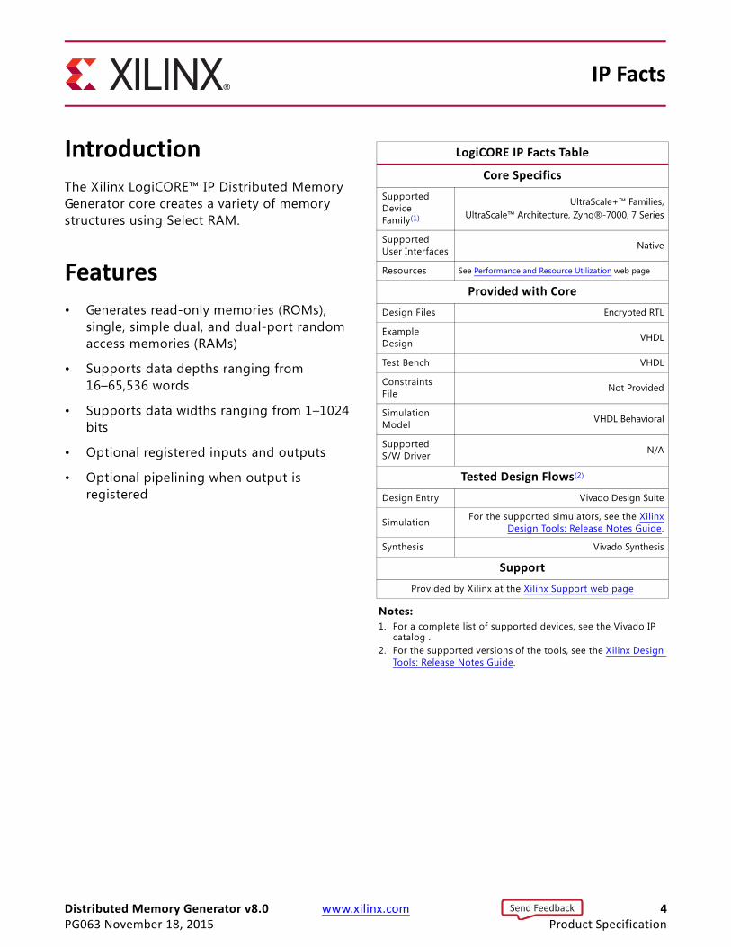
IntroductionThe Xilinx LogiCORE™ IP Distributed Memory Generator core creates a variety of memory structures using Select RAM.
Features• Generates read-only memories (ROMs),
single, simple dual, and dual-port random access memories (RAMs)
• Supports data depths ranging from 16–65,536 words
• Supports data widths ranging from 1–1024 bits
• Optional registered inputs and outputs
• Optional pipelining when output is registered
IP Facts
LogiCORE IP Facts Table
Core SpecificsSupported Device Family(1)
UltraScale+™ Families,UltraScale™ Architecture, Zynq®-7000, 7 Series
Supported User Interfaces Native
Resources See Performance and Resource Utilization web page
Provided with CoreDesign Files Encrypted RTL
Example Design VHDL
Test Bench VHDL
Constraints File Not Provided
Simulation Model VHDL Behavioral
Supported S/W Driver N/A
Tested Design Flows(2)
Design Entry Vivado Design Suite
Simulation For the supported simulators, see the XilinxDesign Tools: Release Notes Guide.
Synthesis Vivado Synthesis
SupportProvided by Xilinx at the Xilinx Support web page
Notes: 1. For a complete list of supported devices, see the Vivado IP
catalog .2. For the supported versions of the tools, see the Xilinx Design
Tools: Release Notes Guide.
Send Feedback
Distributed Memory Generator v8.0 www.xilinx.com 5PG063 November 18, 2015
Chapter 1
OverviewThe Distributed Memory Generator core is used to create memory structures using LUT RAM resources. The core can create the following memory types:
• Distributed ROM, page 10
• Distributed Single-Port RAM, page 11
• Distributed Dual-Port RAM, page 12
• Distributed Simple Dual-Port RAM, page 14
For detailed information about each memory type, see the respective memory type in Chapter 3, Designing with the Core.
Options are available for simple registering of inputs and outputs. Optional asynchronous and synchronous resets are available for the output registers. For timing information, see the Xilinx Product Specif ication for the specif ic target architecture.
Feature SummaryDepth. In all supported FPGA families, the depth can range from 16–65536 words in multiples of 16.
Width. The width of each word can be anywhere in the range of 1–1024 bits.
Optional Input Registering. The following inputs to the memory can be registered or non-registered. When input registering is used, these inputs can be clock-enabled.
• Write Address
• Data
• Write Enable
• Output Register Clock Enable
• Dual-port RAM Read Address
• Simple Dual-port RAM Read Address
Send Feedback
Distributed Memory Generator v8.0 www.xilinx.com 6PG063 November 18, 2015
Chapter 1: Overview
Optional Output Registering and Pipelining. The memory can be non-registered, registered, or both. The output registers can have a variety of controls, including
• Asynchronous Reset
• Synchronous Reset
• Clock Enable
In addition, the Clock Enable and Synchronous Reset can be configured so the Synchronous Reset overrides the Clock Enable, and vice versa. In single-port, simple dual-port and dual-port distributed RAM cores with registered outputs, an additional pipeline register may be added to the output path to improve the operating speed at the expense of an additional cycle of latency.
ApplicationsApplications for Distributed Memory are diverse and numerous. Examples include:
• Using the distributed ROM as a very large look-up table
• Using the single-port RAM as scratch pad memory for embedded PowerPC ™
microprocessors, or for the MicroBlaze ™ or PicoBlaze ™ processors
• Using the simple dual and dual-port RAM within an asynchronous FIFO
Licensing and Ordering InformationThis Xilinx LogiCORE IP module is provided at no additional cost with the Xilinx Vivado Design Suite under the terms of the Xilinx End User License. Information about this and other Xilinx LogiCORE IP modules is available at the Xilinx Intellectual Property page. For information about pricing and availability of other Xilinx LogiCORE IP modules and tools, contact your local Xilinx sales representative.
Send Feedback
Distributed Memory Generator v8.0 www.xilinx.com 7PG063 November 18, 2015
Chapter 2
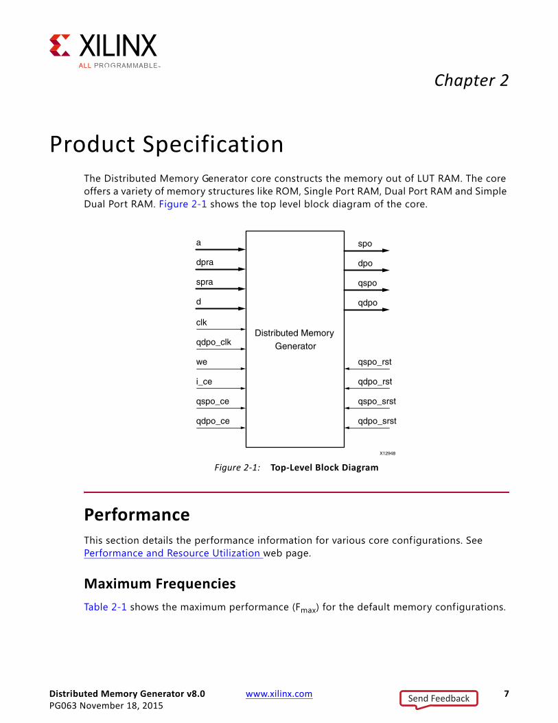
Product SpecificationThe Distributed Memory Generator core constructs the memory out of LUT RAM. The core offers a variety of memory structures like ROM, Single Port RAM, Dual Port RAM and Simple Dual Port RAM. Figure 2-1 shows the top level block diagram of the core.
PerformanceThis section details the performance information for various core configurations. See Performance and Resource Utilization web page.
Maximum FrequenciesTable 2-1 shows the maximum performance (Fmax) for the default memory configurations.
X-Ref Target - Figure 2-1
Figure 2-1: Top-Level Block Diagram
Send Feedback
Distributed Memory Generator v8.0 www.xilinx.com 8PG063 November 18, 2015
Chapter 2: Product Specification
LatencyDepending on the configuration, the Distributed Memory Generator takes either zero or one clock latency to present the read data on the output port. For an asynchronous read (non-registered output), the latency is zero, and for a synchronous read the latency is one.
Resource UtilizationFor details about resource utilization, visit Performance and Resource Utilization web page.
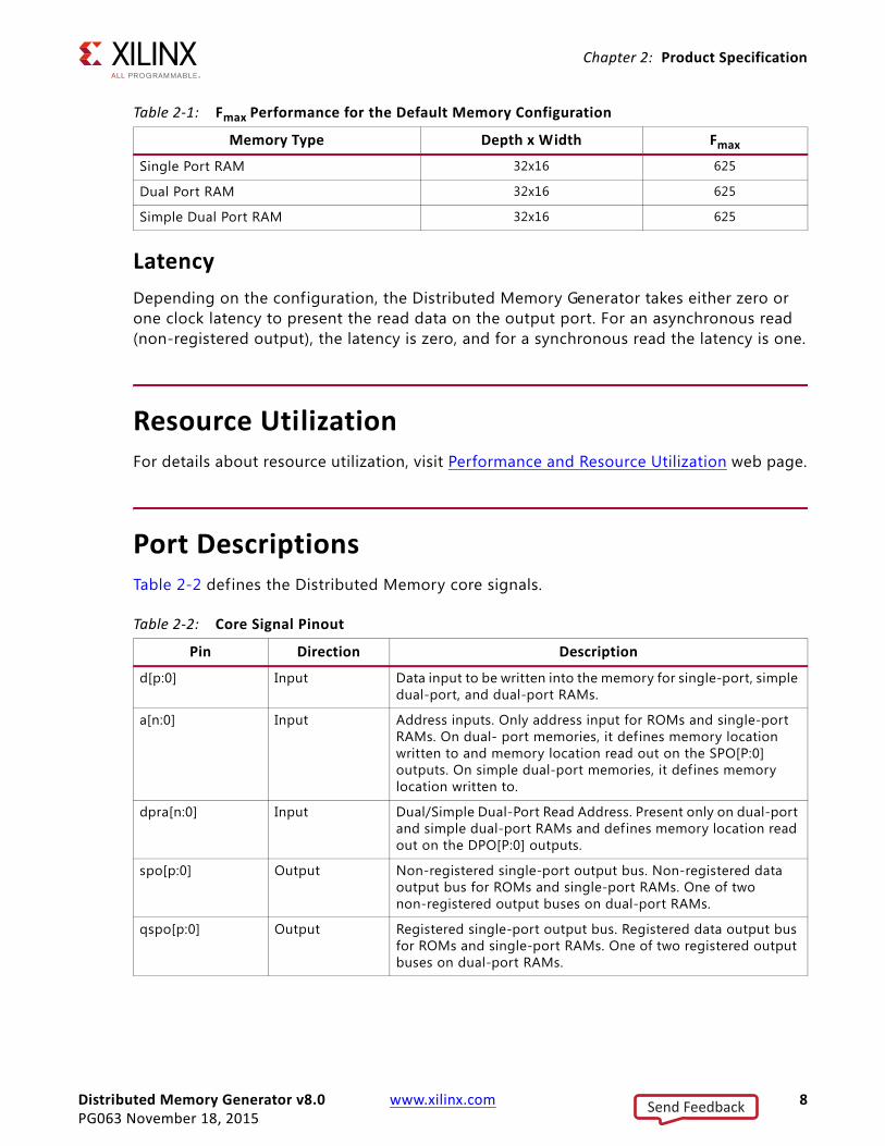
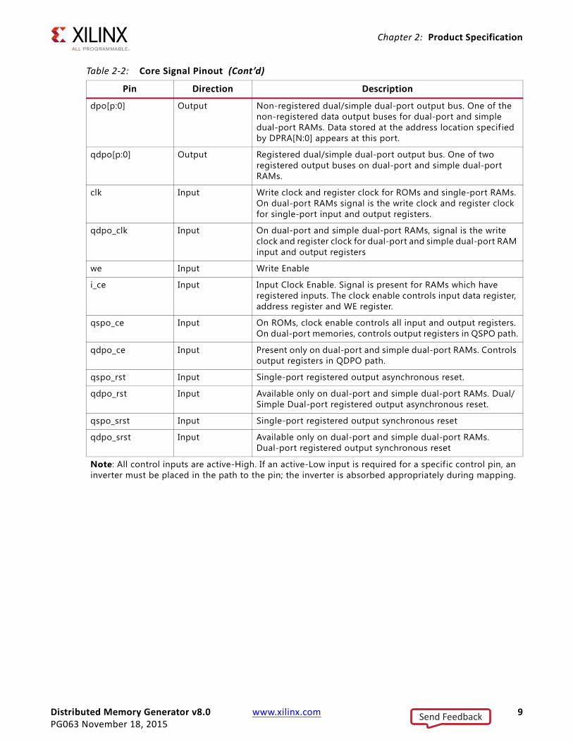
Port DescriptionsTable 2-2 defines the Distributed Memory core signals.
Table 2-1: Fmax Performance for the Default Memory Configuration
Memory Type Depth x Width Fmax
Single Port RAM 32x16 625
Dual Port RAM 32x16 625
Simple Dual Port RAM 32x16 625
Table 2-2: Core Signal Pinout
Pin Direction Description
d[p:0] Input Data input to be written into the memory for single-port, simple dual-port, and dual-port RAMs.
a[n:0] Input Address inputs. Only address input for ROMs and single-port RAMs. On dual- port memories, it defines memory location written to and memory location read out on the SPO[P:0] outputs. On simple dual-port memories, it defines memory location written to.
dpra[n:0] Input Dual/Simple Dual-Port Read Address. Present only on dual-port and simple dual-port RAMs and defines memory location read out on the DPO[P:0] outputs.
spo[p:0] Output Non-registered single-port output bus. Non-registered data output bus for ROMs and single-port RAMs. One of two non-registered output buses on dual-port RAMs.
qspo[p:0] Output Registered single-port output bus. Registered data output bus for ROMs and single-port RAMs. One of two registered output buses on dual-port RAMs.
Send Feedback
Distributed Memory Generator v8.0 www.xilinx.com 9PG063 November 18, 2015
Chapter 2: Product Specification
dpo[p:0] Output Non-registered dual/simple dual-port output bus. One of the non-registered data output buses for dual-port and simple dual-port RAMs. Data stored at the address location specif ied by DPRA[N:0] appears at this port.
qdpo[p:0] Output Registered dual/simple dual-port output bus. One of two registered output buses on dual-port and simple dual-port RAMs.
clk Input Write clock and register clock for ROMs and single-port RAMs. On dual-port RAMs signal is the write clock and register clock for single-port input and output registers.
qdpo_clk Input On dual-port and simple dual-port RAMs, signal is the write clock and register clock for dual-port and simple dual-port RAM input and output registers
we Input Write Enable
i_ce Input Input Clock Enable. Signal is present for RAMs which have registered inputs. The clock enable controls input data register, address register and WE register.
qspo_ce Input On ROMs, clock enable controls all input and output registers. On dual-port memories, controls output registers in QSPO path.
qdpo_ce Input Present only on dual-port and simple dual-port RAMs. Controls output registers in QDPO path.
qspo_rst Input Single-port registered output asynchronous reset.
qdpo_rst Input Available only on dual-port and simple dual-port RAMs. Dual/Simple Dual-port registered output asynchronous reset.
qspo_srst Input Single-port registered output synchronous reset
qdpo_srst Input Available only on dual-port and simple dual-port RAMs. Dual-port registered output synchronous reset
Note: All control inputs are active-High. If an active-Low input is required for a specific control pin, an inverter must be placed in the path to the pin; the inverter is absorbed appropriately during mapping.
Table 2-2: Core Signal Pinout (Cont’d)
Pin Direction Description
Send Feedback
Distributed Memory Generator v8.0 www.xilinx.com 10PG063 November 18, 2015
Chapter 3
Designing with the CoreThis chapter includes guidelines and additional information to make designing with the core easier.
General Design GuidelinesThe following sections provide a functional description and illustration of each of the four memory types.
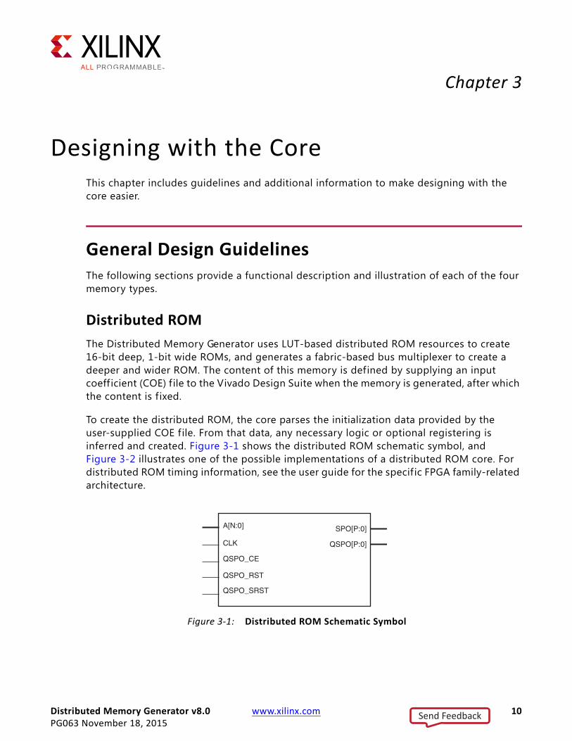
Distributed ROM The Distributed Memory Generator uses LUT-based distributed ROM resources to create 16-bit deep, 1-bit wide ROMs, and generates a fabric-based bus multiplexer to create a deeper and wider ROM. The content of this memory is defined by supplying an input coeff icient (COE) f ile to the Vivado Design Suite when the memory is generated, after which the content is f ixed.
To create the distributed ROM, the core parses the initialization data provided by the user-supplied COE file. From that data, any necessary logic or optional registering is inferred and created. Figure 3-1 shows the distributed ROM schematic symbol, and Figure 3-2 illustrates one of the possible implementations of a distributed ROM core. For distributed ROM timing information, see the user guide for the specif ic FPGA family-related architecture.
X-Ref Target - Figure 3-1
Figure 3-1: Distributed ROM Schematic Symbol
SPO[P:0]
QSPO[P:0]
A[N:0]
CLK
QSPO_CE
QSPO_RST
QSPO_SRST
Send Feedback
Distributed Memory Generator v8.0 www.xilinx.com 11PG063 November 18, 2015
Chapter 3: Designing with the Core
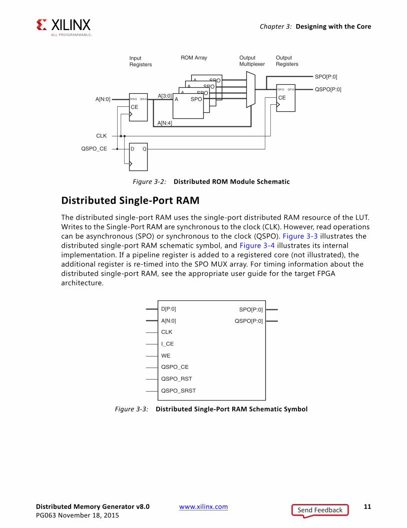
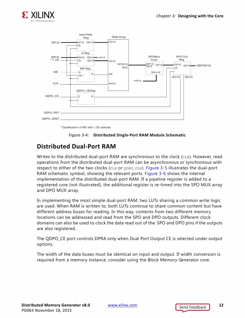
Distributed Single-Port RAMThe distributed single-port RAM uses the single-port distributed RAM resource of the LUT. Writes to the Single-Port RAM are synchronous to the clock (CLK). However, read operations can be asynchronous (SPO) or synchronous to the clock (QSPO). Figure 3-3 illustrates the distributed single-port RAM schematic symbol, and Figure 3-4 illustrates its internal implementation. If a pipeline register is added to a registered core (not illustrated), the additional register is re-timed into the SPO MUX array. For timing information about the distributed single-port RAM, see the appropriate user guide for the target FPGA architecture.
X-Ref Target - Figure 3-2
Figure 3-2: Distributed ROM Module Schematic
X-Ref Target - Figure 3-3
Figure 3-3: Distributed Single-Port RAM Schematic Symbol
A SPOA SPO
A SPOA SPO
CE
CEA[3:0]QSPO[P:0]
SPO[P:0]
ROM Array OutputMultiplexer
OutputRegisters
InputRegisters
A[N:4]
A[N:0]
CLK
QSPO_CE D Q
D[N:0] Q[N:0]
D[P:0] Q[P:0]
D[P:0]
A[N:0]
I_CE
CLK
SPO[P:0]
QSPO[P:0]
WE
QSPO_CE
QSPO_RST
QSPO_SRST
Send Feedback
Distributed Memory Generator v8.0 www.xilinx.com 12PG063 November 18, 2015
Chapter 3: Designing with the Core
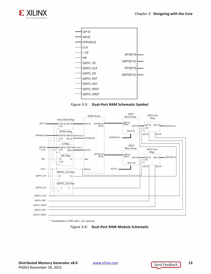
Distributed Dual-Port RAMWrites to the distributed dual-port RAM are synchronous to the clock (CLK). However, read operations from the distributed dual-port RAM can be asynchronous or synchronous with respect to either of the two clocks (CLK or QDPO_CLK). Figure 3-5 illustrates the dual-port RAM schematic symbol, showing the relevant ports. Figure 3-6 shows the internal implementation of the distributed dual-port RAM. If a pipeline register is added to a registered core (not illustrated), the additional register is re-timed into the SPO MUX array and DPO MUX array.
In implementing the most simple dual-port RAM, two LUTs sharing a common write logic are used. When RAM is written to, both LUTs continue to share common content but have different address buses for reading. In this way, contents from two different memory locations can be addressed and read from the SPO and DPO outputs. Different clock domains can also be used to clock the data read out of the SPO and DPO pins if the outputs are also registered.
The QDPO_CE port controls DPRA only when Dual Port Output CE is selected under output options.
The width of the data buses must be identical on input and output. If width conversion is required from a memory instance, consider using the Block Memory Generator core.
X-Ref Target - Figure 3-4
Figure 3-4: Distributed Single-Port RAM Module Schematic
D[P:0]
WE
WCLK
A[3:0]
RAM Array
SPO[P:0]
[M:0]
M[P:0] [M:0]
O[P:0]
S[N-4:0]
CE
SPO OutReg
D[P:0] Q[P:0]
CE
Input DataReg
D[P:0] Q[P:0]
CE
A Reg
D[N:0] Q[N:3]
Q[3:0]
DQ
WE Reg
D Q
QSPO_CEReg
**Qualification of WE with I_CE optional
D[P:0]
WE
CLK
A[N:0] A'[N:4]
QSPO_CE
QSPO[P:0]
**I_CE
CE**
QSPO_RST
ACLR SCLR
QSPO_SRST
A'[N:4]
SPOMuxArray
Send Feedback
Distributed Memory Generator v8.0 www.xilinx.com 13PG063 November 18, 2015
Chapter 3: Designing with the Core
X-Ref Target - Figure 3-5
Figure 3-5: Dual-Port RAM Schematic SymbolX-Ref Target - Figure 3-6
Figure 3-6: Dual-Port RAM Module Schematic
D[P:0]
A[N:0]
DPRA[N:0]
CLK
I_CE
WE
QSPO_CE
QDPO_CLK
QDPO_CE
QSPO_RST
QDPO_RST
QSPO_SRST
QDPO_SRST
SPO[P:0]
QSPO[P:0]
DPO[P:0]
QDPO[P:0]
D[P:0]
DPRA[3:0]
WE
WCLK
A[3:0]
RAM Array
SPO[P:0] [M:0]
DPO[P:0] [M:0]
DPOMux Array
M[P:0][M:0]
O[P:0]
S[N-4:0]
CE
DPO OutReg
D[P:0] Q[P:0]
SPOMux Array
M[P:0][M:0] O[P:0]
S[N-4:0]
CE
SPO OutReg
D[P:0] Q[P:0]
CE
Input Data Reg
D[P:0] Q[P:0]
CE
DPRA Reg
D[N:0] Q[N:3]
CE
A Reg
D[N:0] Q[N:3]
Q[3:0]
Q[3:0]
D Q
WE Reg
D Q
QDPO_CE Reg
D Q
QSPO_CE Reg
D[P:0]
WE
CLK
DPRA[N:0]
A[N:0]
DPRA'[N:4]
A'[N:4]
QDPO_CE
QSPO_CE
QDPO_CLK
QDPO[P:0]
QSPO[P:0]
**I_CE
CE**
** Qualification of WE with I_CE optional
QSPO_RST
SCLR
QDPO_RST
ACLR
ACLR
SCLR
QSPO_SRST
QDPO_SRST
DPRA'[N:4]
A'[N:4]
Send Feedback
Distributed Memory Generator v8.0 www.xilinx.com 14PG063 November 18, 2015
Chapter 3: Designing with the Core
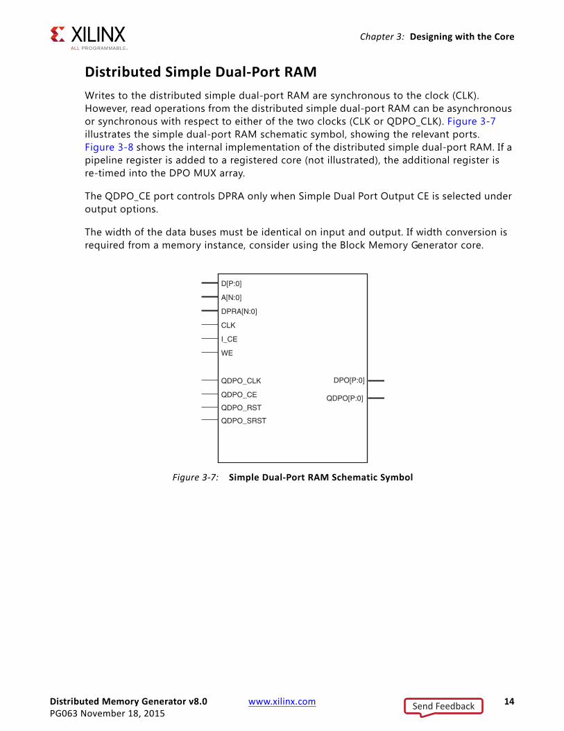
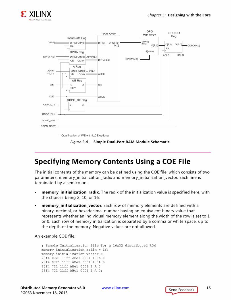
Distributed Simple Dual-Port RAMWrites to the distributed simple dual-port RAM are synchronous to the clock (CLK). However, read operations from the distributed simple dual-port RAM can be asynchronous or synchronous with respect to either of the two clocks (CLK or QDPO_CLK). Figure 3-7 illustrates the simple dual-port RAM schematic symbol, showing the relevant ports. Figure 3-8 shows the internal implementation of the distributed simple dual-port RAM. If a pipeline register is added to a registered core (not illustrated), the additional register is re-timed into the DPO MUX array.
The QDPO_CE port controls DPRA only when Simple Dual Port Output CE is selected under output options.
The width of the data buses must be identical on input and output. If width conversion is required from a memory instance, consider using the Block Memory Generator core.
X-Ref Target - Figure 3-7
Figure 3-7: Simple Dual-Port RAM Schematic Symbol
D[P:0]
A[N:0]
DPRA[N:0]
CLK
I_CE
WE
QDPO_CLK
QDPO_CE
QDPO_RST
QDPO_SRST
DPO[P:0]
QDPO[P:0]
Send Feedback
Distributed Memory Generator v8.0 www.xilinx.com 15PG063 November 18, 2015
Chapter 3: Designing with the Core
Specifying Memory Contents Using a COE FileThe initial contents of the memory can be defined using the COE f ile, which consists of two parameters: memory_initialization_radix and memory_initialization_vector. Each line is terminated by a semicolon.
• memory_initialization_radix. The radix of the initialization value is specif ied here, with the choices being 2, 10, or 16.
• memory_initialization_vector. Each row of memory elements are defined with a binary, decimal, or hexadecimal number having an equivalent binary value that represents whether an individual memory element along the width of the row is set to 1 or 0. Each row of memory initialization is separated by a comma or white space, up to the depth of the memory. Negative values are not allowed.
An example COE f ile:
; Sample Initialization file for a 16x32 distributed ROMmemory_initialization_radix = 16;memory_initialization_vector = 23f4 0721 11ff ABe1 0001 1 0A 023f4 0721 11ff ABe1 0001 1 0A 023f4 721 11ff ABe1 0001 1 A 023f4 721 11ff ABe1 0001 1 A 0;
X-Ref Target - Figure 3-8
Figure 3-8: Simple Dual-Port RAM Module Schematic
D[P:0]
DPRA[3:0]
WE
WCLK
A[3:0]
RAM Array
DPO[P:0] [M:0]
DPOMux Array
M[P:0][M:0]
O[P:0]
S[N-4:0]
CE
DPO OutReg
D[P:0] Q[P:0]CE
Input Data Reg
D[P:0] Q[P:0]
CE
DPRA Reg
D[N:0] Q[N:3]
CE
A Reg
D[N:0] Q[N:3]
Q[3:0]
Q[3:0]
D Q
WE Reg
D Q
QDPO_CE Reg
D[P:0]
WE
CLK
DPRA[N:0]
A[N:0]
DPRA'[N:4]
A'[N:4]
QDPO_CE
QDPO_CLK
QDPO[P:0]
**I_CE
CE**
** Qualification of WE with I_CE optional
QDPO_RST
ACLR SCLR
QDPO_SRST
DPRA'[N:4]
Send Feedback
Distributed Memory Generator v8.0 www.xilinx.com 16PG063 November 18, 2015
Chapter 3: Designing with the Core
MIF File DescriptionThe COE file provides a high-level method for specifying initial memory contents. During core generation, the COE f ile is converted into a MIF f ile, which holds the actual binary data used to initialize the memory in the core and simulation models. The MIF file consists of one line of text per memory location. The first line in the file corresponds to address 0, and the second line corresponds to address 1, and so forth. The text on each line must be the initialization value (MSB first) for the corresponding memory address in binary format, with exactly one binary digit per bit of memory width.
Note: For HDL simulations, the MIF f ile must reside in the simulation directory.
ClockingThe Distributed Memory Generator core has two clocks: clk (write/read clock) and qdpo_clk (read clock). Depending the on the configuration, the core can have either zero, one, or two clocks.
For an asynchronous ROM configuration, there is no clock. For a RAM configuration, the core has a write clock (clk). The same write clock (clk) can be used as a read clock or a separate read clock (qdpo_clk) can also be used.
ResetsThe Distributed Memory Generator core has four resets: two synchronous resets and two asynchronous resets. Depending the on configuration, the core can have any of the following reset options:
• Synchronous reset only
• Asynchronous reset only
• Synchronous and asynchronous resets
• No resets
Send Feedback
Distributed Memory Generator v8.0 www.xilinx.com 17PG063 November 18, 2015
Chapter 4
Design Flow StepsThis chapter describes customizing and generating the core, constraining the core, and the simulation, synthesis and implementation steps that are specific to this IP core. More detailed information about the standard Vivado® design flows and the IP integrator can be found in the following Vivado Design Suite user guides:
• Vivado Design Suite User Guide: Designing IP Subsystems using IP Integrator (UG994) [Ref 2]
• Vivado Design Suite User Guide: Designing with IP (UG896) [Ref 4]
• Vivado Design Suite User Guide: Getting Started (UG910) [Ref 7]
• Vivado Design Suite User Guide: Logic Simulation (UG900) [Ref 1]
Customizing and Generating the CoreThis section includes information about using Xilinx tools to customize and generate the core in the Vivado Design Suite.
If you are customizing and generating the core in the Vivado IP integrator, see the Vivado Design Suite User Guide: Designing IP Subsystems using IP Integrator (UG994) [Ref 2] for detailed information. IP integrator might auto-compute certain configuration values when validating or generating the design. To check whether the values change, see the description of the parameter in this chapter. To view the parameter value, run the validate_bd_design command in the Tcl console.
You can customize the IP for use in your design by specifying values for the various parameters associated with the IP core using the following steps:
1. Select the IP from the IP catalog. Chose one of the following paths to find the core:
° Choose Basic Elements > Memory Elements
° Choose Memories & Storage Elements > RAMs & ROMs
2. Double-click the selected IP or select the Customize IP command from the toolbar or right-click menu.
Send Feedback
Distributed Memory Generator v8.0 www.xilinx.com 18PG063 November 18, 2015
Chapter 4: Design Flow Steps
For details, see the Vivado Design Suite User Guide: Designing with IP (UG896) [Ref 4] and the Vivado Design Suite User Guide: Getting Started (UG910) [Ref 7].
Note: Figures in this chapter are illustrations of the Vivado Integrated Design Environment (IDE). This layout might vary from the current version.
The Distributed Memory Generator GUI uses three screens.
• Main Screen (Figure 4-1)
• Input, Dual-Port, and Output Options Screen (Figure 4-2)
• Initial Content and Reset Options Screen (Figure 4-3)
All the screens share common tabs and buttons to provide information about the core and perform specif ic actions, such as generating the core and navigating among screens.
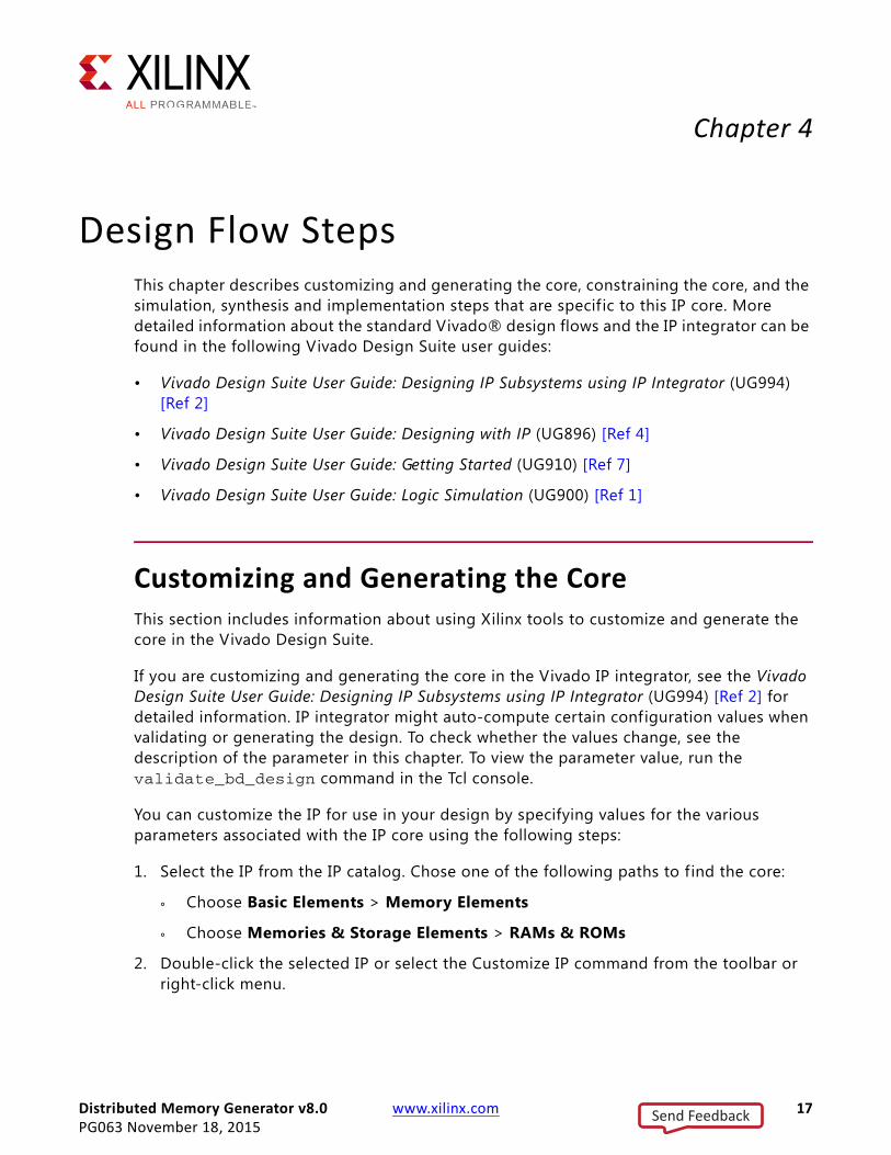
Main Screen
Component Name. The base name of the output f iles generated for the core. Names must begin with a letter and be composed of any of the following characters: a to z, 0 to 9 and “_.”
Depth. Enter a value in the valid range from 16–65536, in steps of 16. Default value is 64.
X-Ref Target - Figure 4-1
Figure 4-1: Main Screen
Send Feedback
Distributed Memory Generator v8.0 www.xilinx.com 19PG063 November 18, 2015
Chapter 4: Design Flow Steps
Data Width: Enter the width of the memory in the valid range from 1–1024. The default value is 16.
Memory Type: Select one of four options. The default setting is single-port RAM.
• ROM. Figure 3-2 is a schematic of the structure of the ROM modules. The address register is optional (controlled by the setting of the Input Options parameter). Output registering is also optional (controlled by the setting of the Output Options parameter). Note that the clock is not required when these registers are not present. The resets and clock enables are optional.
• Single-Port RAM. Figure 3-4 is a schematic of the structure of the single-port RAM modules. The address and data registers are optional (controlled by the setting of the Input Options parameter). Output registering is also optional (controlled by the setting of the Output Options parameter). The resets and clock enables are optional. The clock CLK is always required because writes to the single-port RAM are synchronous to that clock.
• Dual-Port RAM. Figure 3-6 is a schematic of the structure of the dual-port RAM modules. The address and data registers are optional (controlled by the setting of the Input Options parameter). The dual-port read address register is optional (controlled by the setting of the Dual-Port Address parameter). Output registers for both output ports are also optional (controlled by the setting of the Output Options parameter). When registered outputs are selected, the two output ports can be clocked by the same or different clock signals and can have the same or different clock enables (based on the settings selected for the Common Output Clock and Common Output CE parameters). All resets and clock enables are optional. Note that the clock CLK is always required, because writes to the RAM are synchronous to that clock.
• Simple Dual-Port RAM. Figure 3-8 is a schematic of the structure of the simple dual-port RAM modules. The address and data registers are optional (controlled by the setting of the Input Options parameter). The simple dual-port read address register is optional (controlled by the setting of the Simple Dual-Port Address parameter). Output registers for both output ports are also optional (controlled by the setting of the Output Options parameter).
When registered outputs are selected, the output port can be clocked by the same or different clock signals and can have the same or different clock enables (based on the settings selected for the Common Output Clock and Common Output CE parameters). All resets and clock enables are optional. Note that the clock CLK is always required because writes to the RAM are synchronous to that clock.
Send Feedback
Distributed Memory Generator v8.0 www.xilinx.com 20PG063 November 18, 2015
Chapter 4: Design Flow Steps
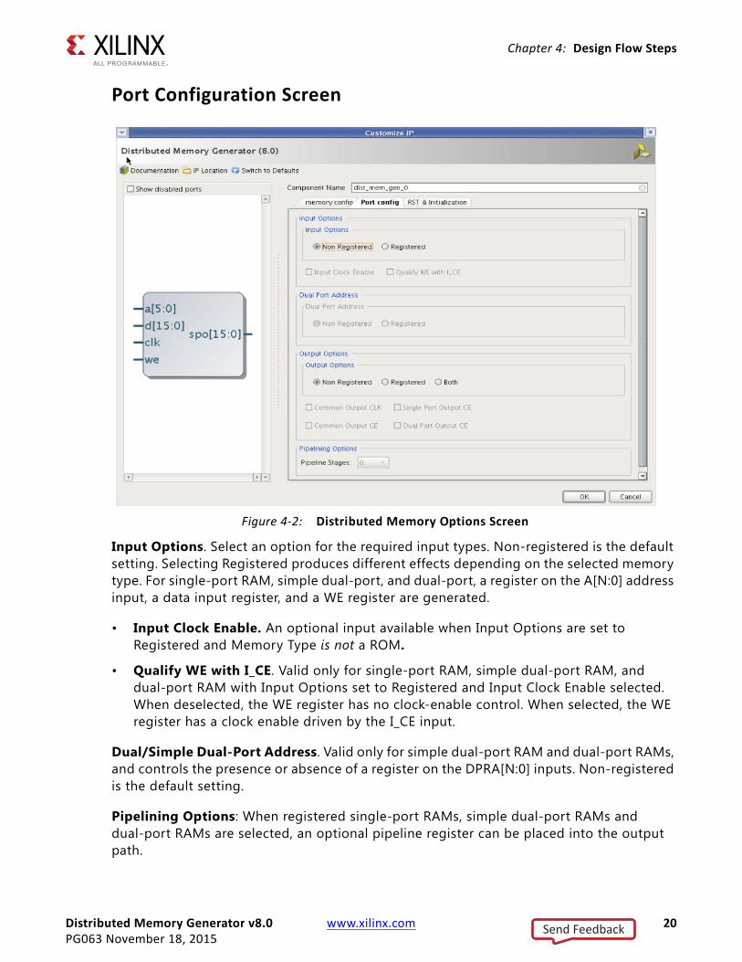
Port Configuration Screen
Input Options. Select an option for the required input types. Non-registered is the default setting. Selecting Registered produces different effects depending on the selected memory type. For single-port RAM, simple dual-port, and dual-port, a register on the A[N:0] address input, a data input register, and a WE register are generated.
• Input Clock Enable. An optional input available when Input Options are set to Registered and Memory Type is not a ROM.
• Qualify WE with I_CE. Valid only for single-port RAM, simple dual-port RAM, and dual-port RAM with Input Options set to Registered and Input Clock Enable selected. When deselected, the WE register has no clock-enable control. When selected, the WE register has a clock enable driven by the I_CE input.
Dual/Simple Dual-Port Address. Valid only for simple dual-port RAM and dual-port RAMs, and controls the presence or absence of a register on the DPRA[N:0] inputs. Non-registered is the default setting.
Pipelining Options: When registered single-port RAMs, simple dual-port RAMs and dual-port RAMs are selected, an optional pipeline register can be placed into the output path.
X-Ref Target - Figure 4-2
Figure 4-2: Distributed Memory Options Screen
Send Feedback
Distributed Memory Generator v8.0 www.xilinx.com 21PG063 November 18, 2015
Chapter 4: Design Flow Steps
• Pipeline Stages. Select 0 for no pipeline registers and 1 for a single pipeline stage in the output multiplexer.
Output Options: Select an option for the required output types. Non-registered is the default setting.
• Single-Port Output Clock Enable. Enabled for registered output memory or for input registered ROM to provide this optional pin.
• Dual/Simple Dual-Port Output Clock Enable. Enabled only for output registered simple dual-port RAM and dual-port RAMs to provide this optional pin.
• Common Output CLK. Enabled only for registered simple dual-port RAMs and dual-port RAMs. If not selected, the SPO registers are clocked by the CLK input and the DPO registers are clocked from the QDPO_CLK input. Default setting is selected, where all output registers are clocked from the CLK input.
• Common Output CE. Enabled only for non-registered simple dual-port RAMs and dual-port RAMs and only if Common Output Clock is also selected. If Common Output CE is deselected, the SPO register clocks are enabled by the QSPO_CE input and the DPO register clocks are enabled from the QDPO_CE input. Default setting is selected, where all output register clocks are enabled by the QSPO_CE input.
Send Feedback
Distributed Memory Generator v8.0 www.xilinx.com 22PG063 November 18, 2015
Chapter 4: Design Flow Steps
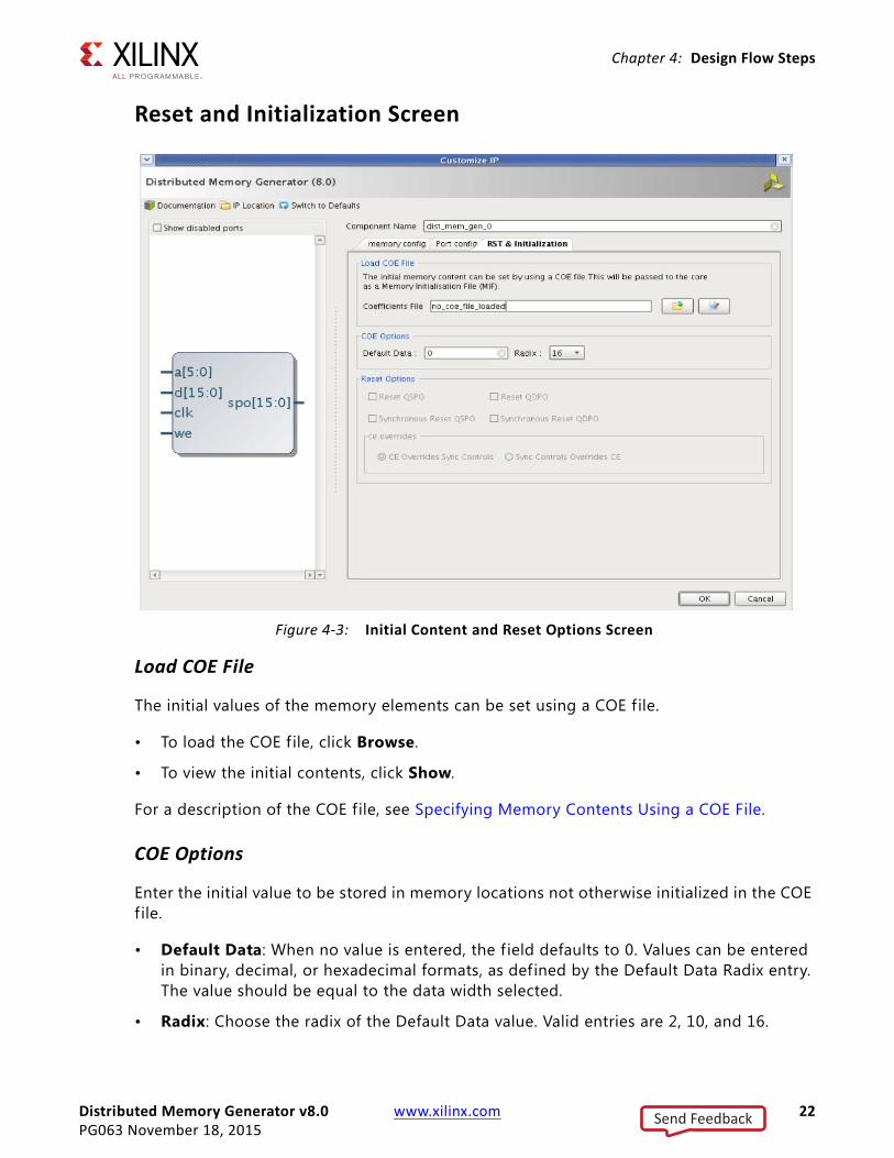
Reset and Initialization Screen
Load COE File
The initial values of the memory elements can be set using a COE f ile.
• To load the COE f ile, click Browse.
• To view the initial contents, click Show.
For a description of the COE file, see Specifying Memory Contents Using a COE File.
COE Options
Enter the initial value to be stored in memory locations not otherwise initialized in the COE f ile.
• Default Data: When no value is entered, the f ield defaults to 0. Values can be entered in binary, decimal, or hexadecimal formats, as defined by the Default Data Radix entry. The value should be equal to the data width selected.
• Radix: Choose the radix of the Default Data value. Valid entries are 2, 10, and 16.
X-Ref Target - Figure 4-3
Figure 4-3: Initial Content and Reset Options Screen
Send Feedback
Distributed Memory Generator v8.0 www.xilinx.com 23PG063 November 18, 2015
Chapter 4: Design Flow Steps
Reset Options
• Reset QSPO: Enabled only when the core has a registered single-port output. If selected, an asynchronous single-port output reset pin is available.
• Reset QDPO: Enabled only when the core has a registered simple dual-port and dual-port output. If selected, an asynchronous simple dual-port and dual-port output reset pin is available.
• Synchronous Reset QSPO: Enabled only when the core has a registered single-port output. If selected, a synchronous single-port output reset pin is available.
• Synchronous Reset QDPO: Enabled only when the core has a registered simple dual-port and dual-port output. If selected, a synchronous simple dual-port and dual-port output reset pin is available.
• CE Overrides Sync Controls: Enabled only when one of the synchronous reset options has been selected and the corresponding output clock enable has been selected. When selected, the synchronous control signals are qualif ied by the clock enable pin.
• Sync Controls Overrides CE: Enabled only when one of the synchronous reset options has been selected and the corresponding output clock enable has been selected. When selected, the synchronous control signals operate regardless of the state of the output clock enable signals.
User ParametersTable 4-1 shows the relationship between the f ields in the Vivado IDE and the User Parameters (which can be viewed in the Tcl Console).
Table 4-1: Vivado IDE Parameter to User Parameter RelationshipVivado IDE Parameter/Value(1) User Parameter/Value(1) Default Value
memory config tab
Options
Depth depth 16
Data Width data_width 16
Memory Type memory_type rom
Port config tab
Input Options input_options Non Registered
Input Clock Enable input_clock_enable 0
Qualify WE with I_CE qualify_we_with_i_ce False
Dual Port Address dual_port_address Non Registered
Output Options output_options Non Registered
Common Output CLK common_output_clk False
Single Port Output CE single_port_output_clock_enable False
Common Output CE common_output_ce False
Send Feedback
Distributed Memory Generator v8.0 www.xilinx.com 24PG063 November 18, 2015
Chapter 4: Design Flow Steps
Output GenerationFor details, the Vivado Design Suite User Guide: Designing with IP (UG896) [Ref 4].
Constraining the CoreThis section contains information about constraining the core in the Vivado Design Suite.
Required ConstraintsIf the write clock (clk) and the read clock (qdpo_clk) are asynchronous to each other:
• Consider using the FIFO generator core. The FIFO generator core has specif ic timing constraints to deal with the write-clock to read-clock timing arcs.
• Alternatively, if the write address is equal to the read address, write the appropriate timing constraints because the resulting timing path is a clock domain crossing path.
Dual Port Output CE dual_port_output_clock_enable False
Pipelining Options
Pipeline Stages Pipeline_Stages 0
RST & Initialization tab
Load COE File
Coeff icients File coeff icient_f ile no_coe_file_loaded
COE Options
Default Data default_data 0
Radix default_data_radix 16
Reset Options
Reset QSPO reset_qspo False
Reset QDPO reset_qdpo False
Synchronous Reset QSPO sync_reset_qspo False
Synchronous Reset QDPO sync_reset_qdpo False
CE Overrides ce_overrides CE Overrides Sync Controls
Notes: 1. Parameter values are listed in the table where the Vivado IDE parameter value differs from the user parameter
value. Such values are shown in this table as indented below the associated parameter.
Table 4-1: Vivado IDE Parameter to User Parameter Relationship (Cont’d)
Vivado IDE Parameter/Value(1) User Parameter/Value(1) Default Value
Send Feedback
Distributed Memory Generator v8.0 www.xilinx.com 25PG063 November 18, 2015
Chapter 4: Design Flow Steps
Device, Package, and Speed Grade SelectionsThis section is not applicable for this IP core.
Clock FrequenciesThis section is not applicable for this IP core.
Clock ManagementThis section is not applicable for this IP core.
Clock PlacementThis section is not applicable for this IP core.
BankingThis section is not applicable for this IP core.
Transceiver PlacementThis section is not applicable for this IP core.
I/O Standard and PlacementThis section is not applicable for this IP core.
SimulationThis section contains information about simulating IP in the Vivado® Design Suite.For details, see the Vivado Design Suite User Guide: Designing with IP (UG896) [Ref 4].
IMPORTANT: For cores targeting 7 series or Zynq-7000 devices, UNIFAST libraries are not supported. Xilinx IP is tested and qualified with UNISIM libraries only.
VHDL behavioral models of Distributed Memory Generator are provided to use within a simulation environment. The functional simulation model for this core is behavioral. Certain conditions such as out-of-range writes are not modelled in a cycle-accurate manner. Run the timing simulation to more closely simulate cycle-based behavior.
Send Feedback
Distributed Memory Generator v8.0 www.xilinx.com 26PG063 November 18, 2015
Chapter 4: Design Flow Steps
Static Timing AnalysisStatic timing analysis can be performed using trce, following ngdbuild, map, and par.
Gate-level SimulationIf desired, the Vivado tools can create a UniSim-based VHDL and Verilog models for gate-level simulation. Alternatively, the netlist produced by the Vivado Synthesis tool (has to be run separately, by using Run Synthesis button in GUI) for the desired memory can be processed using ngdbuild and netgen to produce a SimPrim-based model for simulation.
Messages and WarningsWhen the functional or timing simulation has completed successfully, the test bench displays the following message, and it is safe to ignore this message.
Failure: Test Completed Successfully
Synthesis and ImplementationFor details about synthesis and implementation, see the Vivado Design Suite User Guide: Designing with IP (UG896) [Ref 4].
Send Feedback
Distributed Memory Generator v8.0 www.xilinx.com 27PG063 November 18, 2015
Chapter 5
Detailed Example DesignThis chapter provides detailed information about the example design, including a description of f iles and the directory structure generated by the Xilinx Vivado tools, the purpose and contents of the provided scripts and the contents of the example HDL wrappers.
Directory and File ContentsFor details about the f iles created with the example design, see the Vivado Design Suite User Guide: Designing with IP (UG896) [Ref 4].
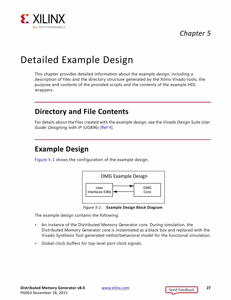
Example DesignFigure 5-1 shows the configuration of the example design.
The example design contains the following:
• An instance of the Distributed Memory Generator core. During simulation, the Distributed Memory Generator core is instantiated as a black box and replaced with the Vivado Synthesis Tool generated netlist/behavioral model for the functional simulation.
• Global clock buffers for top-level port clock signals.
X-Ref Target - Figure 5-1
Figure 5-1: Example Design Block Diagram
Send Feedback
Distributed Memory Generator v8.0 www.xilinx.com 28PG063 November 18, 2015
Chapter 6
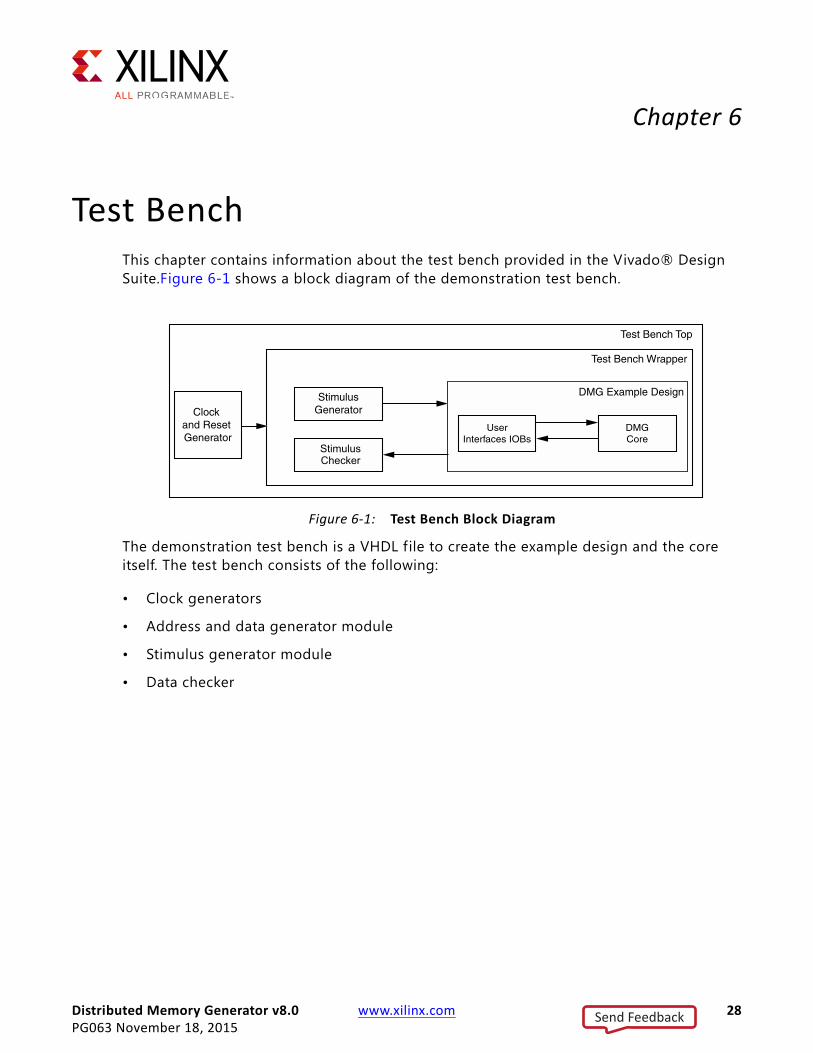
Test BenchThis chapter contains information about the test bench provided in the Vivado® Design Suite.Figure 6-1 shows a block diagram of the demonstration test bench.
The demonstration test bench is a VHDL file to create the example design and the core itself. The test bench consists of the following:
• Clock generators
• Address and data generator module
• Stimulus generator module
• Data checker
X-Ref Target - Figure 6-1
Figure 6-1: Test Bench Block Diagram
Send Feedback
Distributed Memory Generator v8.0 www.xilinx.com 29PG063 November 18, 2015
Appendix A
Verification, Compliance, and Interoperability
Xilinx has verif ied the Distributed Memory Generator core in a proprietary test environment, using an internally developed bus functional model. Tens of thousands of test vectors were generated and verif ied, including both valid and invalid write and read data accesses.
SimulationThe Distributed Memory Generator has been tested with the Xilinx Vivado Design Suite, Xilinx ISIM/XSIM, and Mentor Graphics Questa SIM.
Send Feedback

Distributed Memory Generator v8.0 www.xilinx.com 30PG063 November 18, 2015
Appendix B
DebuggingThis appendix includes details about resources available on the Xilinx Support website and debugging tools. In addition, this appendix provides a step-by-step debugging process and a flow diagram to guide you through debugging the Distributed Memory Generator core.
Finding Help on Xilinx.comTo help in the design and debug process when using the Distributed Memory Generator, the Xilinx Support web page contains key resources such as product documentation, release notes, answer records, information about known issues, and links for opening a Technical Support WebCase.
DocumentationThis product guide is the main document associated with the Distributed Memory Generator. This guide, along with documentation related to all products that aid in the design process, can be found on the Xilinx Support web page or by using the Xilinx Documentation Navigator.
Download the Xilinx Documentation Navigator from the Downloads page. For more information about this tool and the features available, open the online help after installation.
Answer RecordsAnswer Records include information about commonly encountered problems, helpful information on how to resolve these problems, and any known issues with a Xilinx product. Answer Records are created and maintained daily ensuring that users have access to the most accurate information available.
Answer Records for this core are listed below, and can be located by using the Search Support box on the main Xilinx support web page. To maximize your search results, use proper keywords such as
• Product name
• Tool message(s)
Send Feedback
Distributed Memory Generator v8.0 www.xilinx.com 31PG063 November 18, 2015
Appendix B: Debugging
• Summary of the issue encountered
A filter search is available after results are returned to further target the results.
Distributed Memory Generator Master Answer Record
AR: 54661
Technical SupportXilinx provides technical support in the Xilinx Support web page for this LogiCORE™ IP product when used as described in the product documentation. Xilinx cannot guarantee timing, functionality, or support if you do any of the following:
• Implement the solution in devices that are not defined in the documentation.
• Customize the solution beyond that allowed in the product documentation.
• Change any section of the design labeled DO NOT MODIFY.
To contact Xilinx Technical Support, navigate to the Xilinx Support web page.
• Target device including package and speed grade.
Debug ToolsThere are many tools available to address Distributed Memory Generator design issues. It is important to know which tools are useful for debugging various situations.
Vivado Design Suite Debug FeatureVivado® Lab Edition inserts logic analyzer and virtual I/O cores directly into your design. Vivado Lab Edition also allows you to set trigger conditions to capture application and integrated block port signals in hardware. Captured signals can then be analyzed. This feature in the Vivado IDE is used for logic debugging and validation of a design running in Xilinx.
The Vivado logic analyzer is used to interact with the logic debug LogiCORE IP cores, including:
• ILA 2.0 (and later versions)
• VIO 2.0 (and later versions)
Send Feedback
Distributed Memory Generator v8.0 www.xilinx.com 32PG063 November 18, 2015
Appendix B: Debugging
Simulation DebugFor details about simulating a design in the Vivado Design Suite, see the Vivado Logic Simulation User Guide (UG900) [Ref 1].
Hardware DebugHardware issues can range from link bring-up to problems seen after hours of testing. This section provides debug steps for common issues.
General ChecksEnsure that all the timing constraints for the core were properly incorporated from the example design and that all constraints were met during implementation.
• Does it work in post-place and route timing simulation? If problems are seen in hardware but not in timing simulation, this could indicate a PCB issue. Ensure that all clock sources are active and clean.
• If using MMCMs in the design, ensure that all MMCMs have obtained lock by monitoring the locked port.
• If your outputs go to 0, check your licensing.
• Ensure we, i_ce, qspo_ce, and qdpo_ce are not toggling during reset.
Interface Debug
Memory InterfacesIf the data is not being written, check the following conditions:
• Check if the core is in reset state.
• Check if d and a is stable and meeting setup/hold window.
• Check if we and i_ce are High and meeting setup/hold window during the write operation.
If the data is not being read, check the following conditions:
• Check if the core is in reset state.
• Check if dpra and a are stable and meeting setup/hold window.
Send Feedback
Distributed Memory Generator v8.0 www.xilinx.com 33PG063 November 18, 2015
Appendix B: Debugging
• Check if qspo_ce and qdpo_ce are High and meeting setup/hold window during the read operation.
Send Feedback
Distributed Memory Generator v8.0 www.xilinx.com 34PG063 November 18, 2015
Appendix C
Migrating and UpgradingThis appendix contains information about migrating a design from ISE® to the Vivado® Design Suite, and for upgrading to a more recent version of the IP core. For customers upgrading in the Vivado Design Suite, important details (where applicable) about any port changes and other impact to user logic are included.
Migrating to the Vivado Design SuiteFor information about migrating to the Vivado Design Suite, see the ISE to Vivado Design Suite Migration Guide (UG911) [Ref 8].
Upgrading in the Vivado Design SuiteThis section provides information about any changes to the user logic or port designations that take place when you upgrade to a more current version of this IP core in the Vivado Design Suite.
Parameter Changes There were no parameter changes in this version of the core.
Port ChangesAn unused port (SPRA) has been removed from v8.0 of the core.
Send Feedback
Distributed Memory Generator v8.0 www.xilinx.com 35PG063 November 18, 2015
Appendix D
Additional Resources and Legal Notices
Xilinx ResourcesFor support resources such as Answers, Documentation, Downloads, and Forums, see Xilinx Support.
References1. Vivado Design Suite User Guide: Logic Simulation (UG900)
2. Vivado Design Suite User Guide: Designing IP Subsystems using IP Integrator (UG994)
3. Vivado Design Suite User Guide: Implementation (UG904)
4. Vivado Design Suite User Guide: Designing with IP (UG896)
5. Vivado Design Suite Migration Methodology Guide (UG911)
6. Vivado Design Suite User Guide: Programming and Debugging (UG908)
7. Vivado Design Suite User Guide: Getting Started (UG910)
8. ISE to Vivado Design Suite Migration Methodology Guide (UG911)
Send Feedback

Distributed Memory Generator v8.0 www.xilinx.com 36PG063 November 18, 2015
Appendix D: Additional Resources and Legal Notices
Revision HistoryThe following table shows the revision history for this document.
Please Read: Important Legal NoticesThe information disclosed to you hereunder (the "Materials") is provided solely for the selection and use of Xilinx products. To the maximum extent permitted by applicable law: (1) Materials are made available "AS IS" and with all faults, Xilinx hereby DISCLAIMS ALL WARRANTIES AND CONDITIONS, EXPRESS, IMPLIED, OR STATUTORY, INCLUDING BUT NOT LIMITED TO WARRANTIES OF MERCHANTABILITY, NON-INFRINGEMENT, OR FITNESS FOR ANY PARTICULAR PURPOSE; and (2) Xilinx shall not be liable (whether in contract or tort, including negligence, or under any other theory of liability) for any loss or damage of any kind or nature related to, arising under, or in connection with, the Materials (including your use of the Materials), including for any direct, indirect, special, incidental, or consequential loss or damage (including loss of data, profits, goodwill, or any type of loss or damage suffered as a result of any action brought by a third party) even if such damage or loss was reasonably foreseeable or Xilinx had been advised of the possibility of the same. Xilinx assumes no obligation to correct any errors contained in the Materials or to notify you of updates to the Materials or to product specifications. You may not reproduce, modify, distribute, or publicly display the Materials without prior written consent. Certain products are subject to the terms and conditions of Xilinx's limited warranty, please refer to Xilinx's Terms of Sale which can be viewed at http://www.xilinx.com/legal.htm#tos; IP cores may be subject to warranty and support terms contained in a license issued to you by Xilinx. Xilinx products are not designed or intended to be fail-safe or for use in any application requiring fail-safe performance; you assume sole risk and liability for use of Xilinx products in such critical applications, please refer to Xilinx's Terms of Sale which can be viewed at http://www.xilinx.com/legal.htm#tos.© Copyright 2012-2015 Xilinx, Inc. Xilinx, the Xilinx logo, Artix, ISE, Kintex, Spartan, Virtex, Vivado, Zynq, and other designated brands included herein are trademarks of Xilinx in the United States and other countries. All other trademarks are the property of their respective owners.
Date Version Revision
11/18/2015 8.0 • Added support for UltraScale+ architecture-based devices.
09/30/2015 8.0 • Removed verilog simulations from delivery.
04/01/2015 8.0 • Updated Required Constraints section.• Updated Test Bench Block Diagram.• Added User Parameters section.
12/18/2013 8.0 • Added support for UltraScale™ architecture.• Added Simulation, Synthesis and Implementation, and Test Bench
chapters.• Updated document revision version to align with core version 8.0.
03/20/2013 2.0 • Updated for core v8.0.• Removed support for ISE Design Suite. • Removed the unused port SPRA.
07/252012 1.0 Initial Xilinx release as a Product Guide. Replaces DS322, LogiCORE IP Distributed Memory Generator Data Sheet. Added support for Vivado Design Suite.
Send Feedback


![Distributed Shared Memory Distributed Memory[1]](https://img.pdfslide.net/doc/110x75/577d23271a28ab4e1e991e57/distributed-shared-memory-distributed-memory1.jpg)