Embed Size (px)
Citation preview
National Aeronautics and Space Administration
Disturb Testing in Flash Memories
Douglas Sheldon Jet Propulsion Laboratory
California Institute of Technology Pasadena, California
Michael Freie
Semiconductor Solutions, Inc. Sparks, Nevada
Jet Propulsion Laboratory California Institute of Technology
Pasadena, California
JPL Publication 08-7 3/08

National Aeronautics and Space Administration
Disturb Testing in Flash Memories
NASA Electronic Parts and Packaging (NEPP) Program Office of Safety and Mission Assurance
Douglas Sheldon Jet Propulsion Laboratory
California Institute of Technology Pasadena, California
Micheal Freie
Semiconductor Solutions, Inc. Sparks, Nevada
NASA WBS: 939904.01.11-10 JPL Project Number: 102197
Task Number: 1.23.6
Jet Propulsion Laboratory 4800 Oak Grove Drive Pasadena, CA 91109
http://nepp.nasa.gov
ii
This research was carried out at the Jet Propulsion Laboratory, California Institute of
Technology, and was sponsored by the National Aeronautics and Space Administration
Electronic Parts and Packaging (NEPP) Program.
Reference herein to any specific commercial product, process, or service by trade name,
trademark, manufacturer, or otherwise, does not constitute or imply its endorsement by the
United States Government or the Jet Propulsion Laboratory, California Institute of Technology.
Copyright 2008. All rights reserved.
iii
Table of Contents
Executive Summary ........................................................................................................................ 1 Introduction..................................................................................................................................... 2 Review of Flash Memory Technology ........................................................................................... 2 NAND Flash Memory Operation.................................................................................................... 6 NAND Flash Errors Modes ............................................................................................................ 7 Disturb Errors.................................................................................................................................. 8 Bad Blocks .................................................................................................................................... 10 Device Programming Details........................................................................................................ 11 Experimental Results .................................................................................................................... 14 Conclusions................................................................................................................................... 20 References..................................................................................................................................... 21
1/26 Disturb Testing Flash Memories Sheldon
Executive Summary
2Gb NAND flash devices were tested for sensitivity to both program and read disturb conditions.
This disturb testing is part of the overall reliability evaluation of these devices for use on NASA
missions. Radiation evaluation for these devices has already been documented [Irom].
Disturb testing is designed to study the robustness of the data storage of the flash cells when the
state of a nearby cell is being changed, either through programming or reading. A disturb failure
means that the initial (and expected) state of the cell has been changed (disturbed) to the opposite
state as a result of programming or reading the nearby cells. Disturb failures are usually soft
failures that require additional device commands to repair.
Flash manufacturers acknowledge disturb failures can occur on their devices and try to provide
users with guidance on how to address them. For the high reliability nature of NASA missions, a
quantitative understanding of the possible degree of disturb failures is required. Such quantitative
understanding will guide device screening and procurement requirements as well as possible
system mitigation implementations.
No specific disturb failures were noted on the testing done for this report. However, inconsistent
behavior in flash memory bad blocks was observed. Block locations that were initially identified
as bad by the manufacturer performed correctly as the device began to be exercised. These
locations remained robust even as the device was stressed over time and temperature.
Other cells marked as good by the manufacturer began to degrade under this exposure to time
and temperature. The associated failure rate with this degradation is 100X higher than predicted
by the manufacturer’s data. At this time, it is unknown why such a high failure rate was
observed.
The existence of this much higher failure rate and inconsistency in manufacturer-defined bad and
good blocks means that NASA must individually screen, characterize, and qualify any and all
NAND flash devices that it intends to use for spacecraft applications.
2/26 Disturb Testing Flash Memories Sheldon
Introduction
Non-volatile memory technology as defined by NAND architecture flash memory continues to
lead the process scaling and device shrinking efforts of the entire integrated circuit industry. 45-
nm technology nodes are now producing commercial 32Gb devices. These latest 32Gb devices
are pioneering new charge trapping memory cell technologies using metal gates and high-k
dielectric materials. These cells are called TANOS and consist of tantalum-nitride, aluminum
oxide (high k material), nitride, oxide, and silicon. Such high-density memories continue to
revolutionize commercial electronics in terms of new high-speed data architectures and
significant reductions in overall power and weight consumption.
In stark contrast, nearly all science-based interplanetary and earth-orbiting NASA spacecraft are
still designing in and around mid-1980s-level non-volatile technology with 1Mb Electrically
Erasable Read-Only Memory (EEPROM) devices. NASA has typically shunned the use of
modern flash devices because of radiation and reliability concerns due to the commercial-off-
the–shelf (COTS) nature of the NAND flash technology. Given the significant potential
increases in overall system capability these modern flash devices could bring to NASA missions,
it is important to continue to investigate these devices. This report will investigate certain
portions of the reliability performance of NAND flash devices, specifically the disturb
properties. Understanding the possible limitations such new non-volatile memory technology
presents to NASA is the goal of this report.
Review of Flash Memory Technology
There are two primary types of NAND flash technology. Historically, the majority of the market
was served by single-level cell (SLC) NAND. Beginning in 2006, the market has migrated to
multi-level cell (MLC) NAND, and by the end of the year, there was a nearly even distribution in
shipments between the two types of cells [Cooke]. From 2007 and on, it is expected that the
majority of shipments will be MLC NAND. However, SLC will retain much of the market for
high-performance, high-reliability applications. SLC is the style device that will be examined for
this report.
3/26 Disturb Testing Flash Memories Sheldon
From a commercial point-of-view, MLC NAND tends to be used in low-cost consumer
applications, including media players, MP3 devices, media cards, and USB flash drives.
Meanwhile, professional products and solid state drives (SSDs) demand the higher performance
and reliability of SLC NAND flash memory.
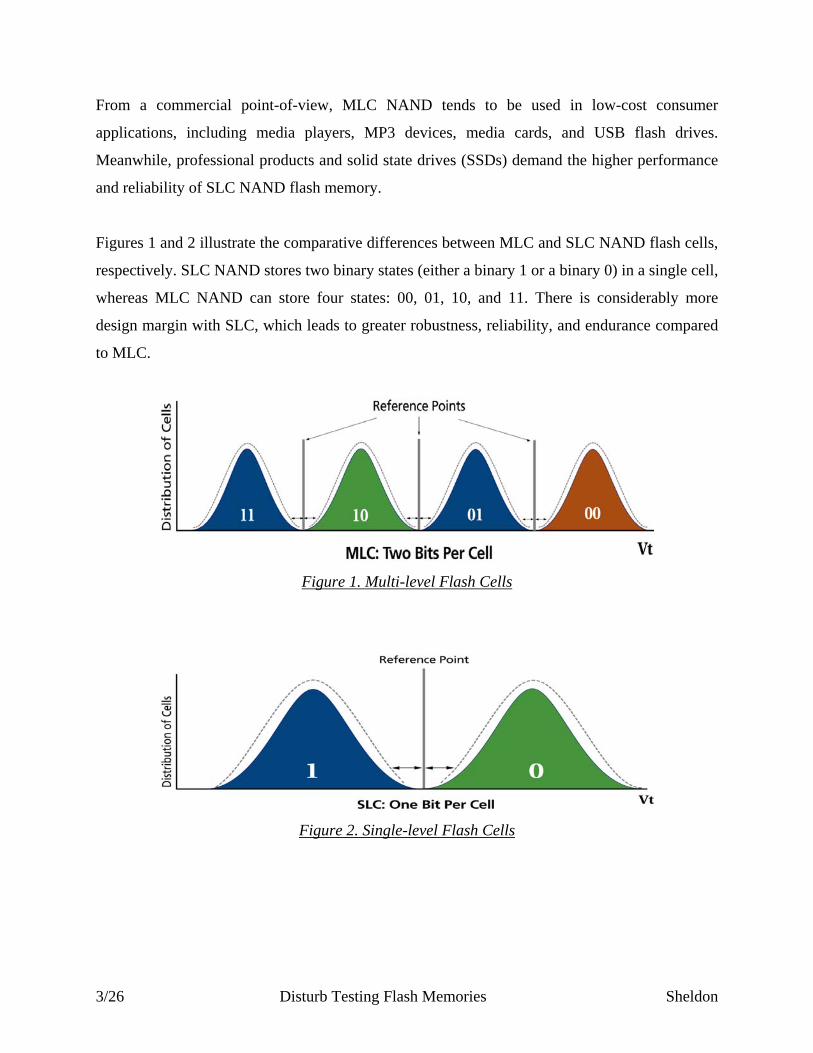
Figures 1 and 2 illustrate the comparative differences between MLC and SLC NAND flash cells,
respectively. SLC NAND stores two binary states (either a binary 1 or a binary 0) in a single cell,
whereas MLC NAND can store four states: 00, 01, 10, and 11. There is considerably more
design margin with SLC, which leads to greater robustness, reliability, and endurance compared
to MLC.
Figure 1. Multi-level Flash Cells
Figure 2. Single-level Flash Cells
4/26 Disturb Testing Flash Memories Sheldon
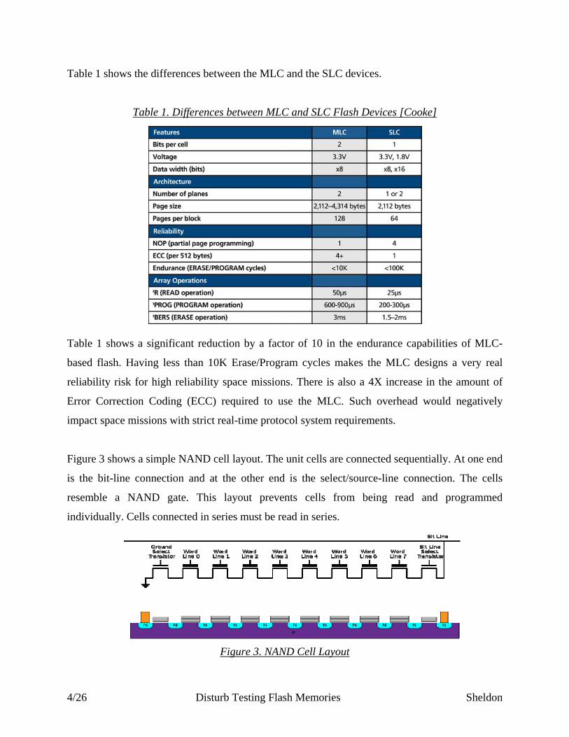
Table 1 shows the differences between the MLC and the SLC devices.
Table 1. Differences between MLC and SLC Flash Devices [Cooke]
Table 1 shows a significant reduction by a factor of 10 in the endurance capabilities of MLC-
based flash. Having less than 10K Erase/Program cycles makes the MLC designs a very real
reliability risk for high reliability space missions. There is also a 4X increase in the amount of
Error Correction Coding (ECC) required to use the MLC. Such overhead would negatively
impact space missions with strict real-time protocol system requirements.
Figure 3 shows a simple NAND cell layout. The unit cells are connected sequentially. At one end
is the bit-line connection and at the other end is the select/source-line connection. The cells
resemble a NAND gate. This layout prevents cells from being read and programmed
individually. Cells connected in series must be read in series.
Figure 3. NAND Cell Layout
5/26 Disturb Testing Flash Memories Sheldon
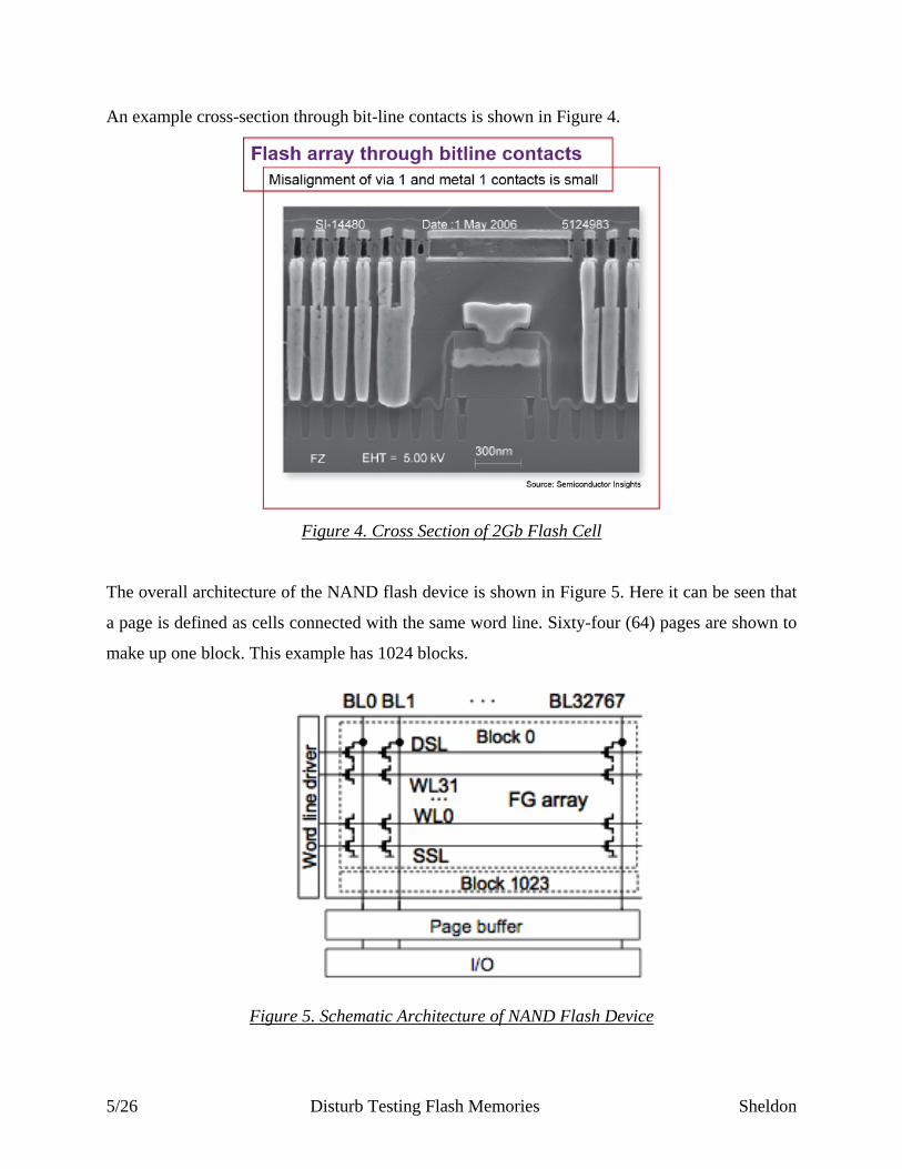
An example cross-section through bit-line contacts is shown in Figure 4.
Figure 4. Cross Section of 2Gb Flash Cell
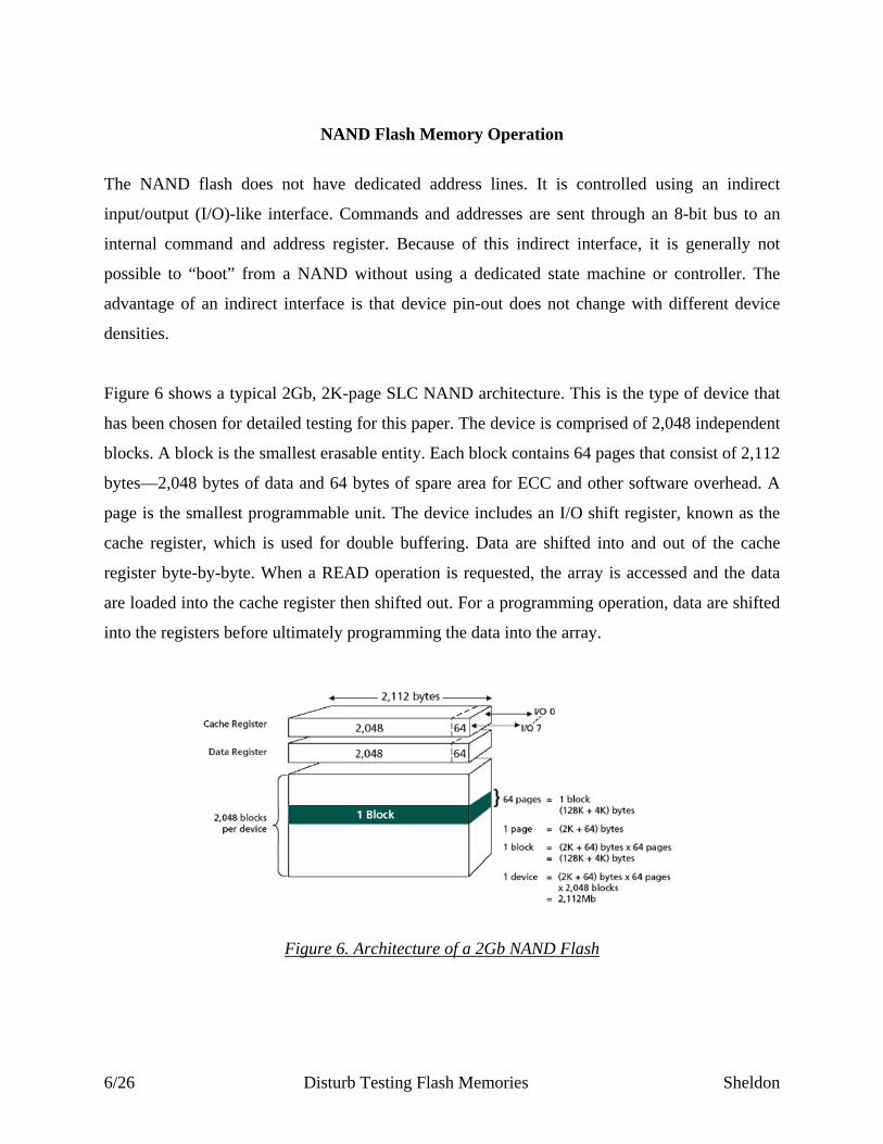
The overall architecture of the NAND flash device is shown in Figure 5. Here it can be seen that
a page is defined as cells connected with the same word line. Sixty-four (64) pages are shown to
make up one block. This example has 1024 blocks.
Figure 5. Schematic Architecture of NAND Flash Device
6/26 Disturb Testing Flash Memories Sheldon
NAND Flash Memory Operation
The NAND flash does not have dedicated address lines. It is controlled using an indirect
input/output (I/O)-like interface. Commands and addresses are sent through an 8-bit bus to an
internal command and address register. Because of this indirect interface, it is generally not
possible to “boot” from a NAND without using a dedicated state machine or controller. The
advantage of an indirect interface is that device pin-out does not change with different device
densities.
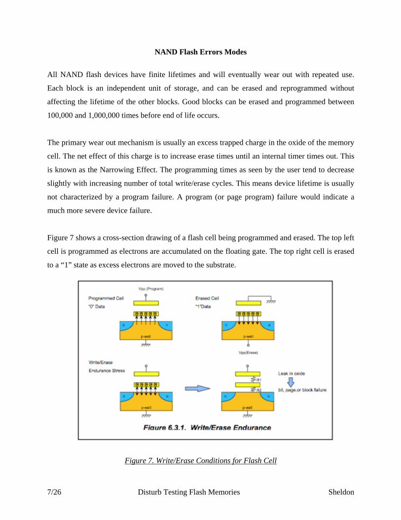
Figure 6 shows a typical 2Gb, 2K-page SLC NAND architecture. This is the type of device that
has been chosen for detailed testing for this paper. The device is comprised of 2,048 independent
blocks. A block is the smallest erasable entity. Each block contains 64 pages that consist of 2,112
bytes—2,048 bytes of data and 64 bytes of spare area for ECC and other software overhead. A
page is the smallest programmable unit. The device includes an I/O shift register, known as the
cache register, which is used for double buffering. Data are shifted into and out of the cache
register byte-by-byte. When a READ operation is requested, the array is accessed and the data
are loaded into the cache register then shifted out. For a programming operation, data are shifted
into the registers before ultimately programming the data into the array.
Figure 6. Architecture of a 2Gb NAND Flash
7/26 Disturb Testing Flash Memories Sheldon
NAND Flash Errors Modes
All NAND flash devices have finite lifetimes and will eventually wear out with repeated use.
Each block is an independent unit of storage, and can be erased and reprogrammed without
affecting the lifetime of the other blocks. Good blocks can be erased and programmed between
100,000 and 1,000,000 times before end of life occurs.
The primary wear out mechanism is usually an excess trapped charge in the oxide of the memory
cell. The net effect of this charge is to increase erase times until an internal timer times out. This
is known as the Narrowing Effect. The programming times as seen by the user tend to decrease
slightly with increasing number of total write/erase cycles. This means device lifetime is usually
not characterized by a program failure. A program (or page program) failure would indicate a
much more severe device failure.
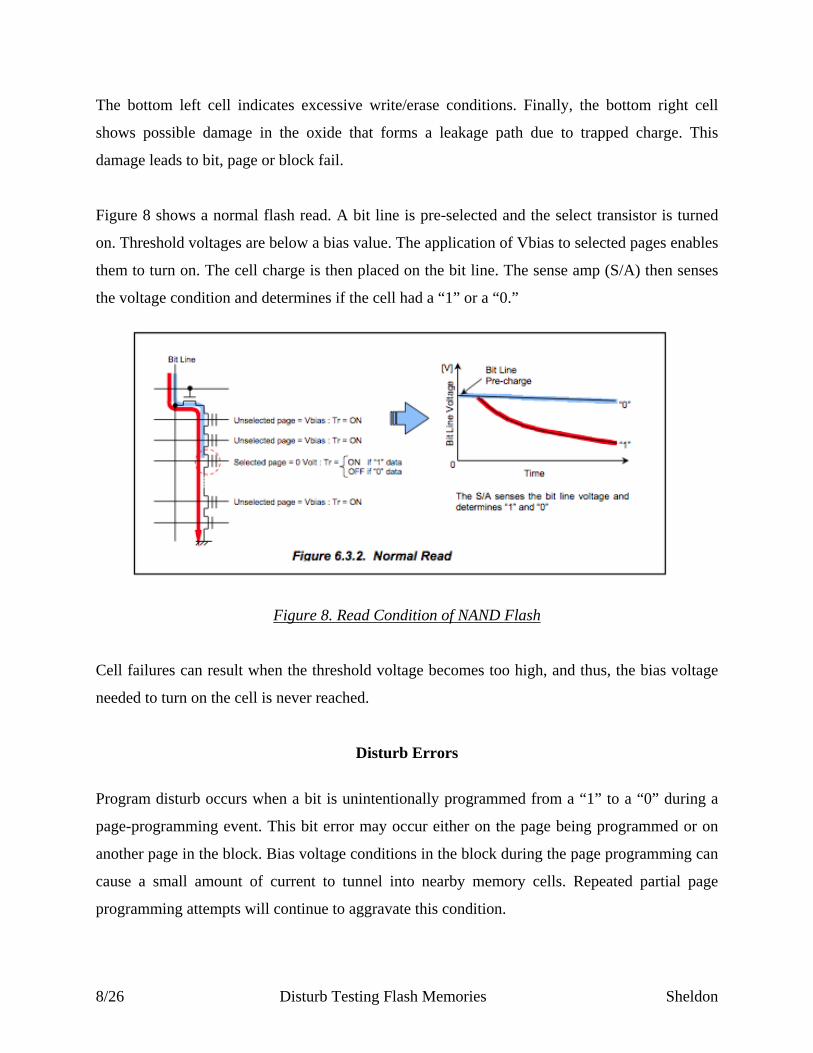
Figure 7 shows a cross-section drawing of a flash cell being programmed and erased. The top left
cell is programmed as electrons are accumulated on the floating gate. The top right cell is erased
to a “1” state as excess electrons are moved to the substrate.
Figure 7. Write/Erase Conditions for Flash Cell
8/26 Disturb Testing Flash Memories Sheldon
The bottom left cell indicates excessive write/erase conditions. Finally, the bottom right cell
shows possible damage in the oxide that forms a leakage path due to trapped charge. This
damage leads to bit, page or block fail.
Figure 8 shows a normal flash read. A bit line is pre-selected and the select transistor is turned
on. Threshold voltages are below a bias value. The application of Vbias to selected pages enables
them to turn on. The cell charge is then placed on the bit line. The sense amp (S/A) then senses
the voltage condition and determines if the cell had a “1” or a “0.”
Figure 8. Read Condition of NAND Flash
Cell failures can result when the threshold voltage becomes too high, and thus, the bias voltage
needed to turn on the cell is never reached.
Disturb Errors
Program disturb occurs when a bit is unintentionally programmed from a “1” to a “0” during a
page-programming event. This bit error may occur either on the page being programmed or on
another page in the block. Bias voltage conditions in the block during the page programming can
cause a small amount of current to tunnel into nearby memory cells. Repeated partial page
programming attempts will continue to aggravate this condition.
9/26 Disturb Testing Flash Memories Sheldon
It is known that program/erase cycling of flash memories induces a degradation of the tunnel
oxide insulating property usually referred to as Stress-Induced Leakage Current (SILC). Read
disturb can be related to SILC conditions [Yang].
With a condition of SILC, a read disturb can manifest itself as affecting cells in an addressed
word-line. This results in electron injection through the tunnel oxide in the floating gate of erased
cells during read operation. Read disturb can also be present in Flash memory with a weak tunnel
oxide quality [Tanduo].
Error modes for NAND include program disturb, read disturb, and endurance. Each error-mode
issue is well understood and easily addressed. It is mandatory to use the minimum ECC specified
for reliable systems. Using more robust ECC schemes will provide additional system reliability.
In some cases, program and read operations may cause electrons to move to or from other cells
within the block.
To reduce program disturb, it is recommended to sequentially program pages in a block. It is also
important to minimize partial-page programming operations in SLC devices, and it is mandatory
to restrict page programming to a single operation in MLC.
Read disturb can be reduced by minimizing excessive reads. The rule of thumb is no more than 1
million READ cycles (per block) for SLC, and a maximum of 100,000 READ cycles for MLC.
If possible, the data should be read equally from pages within the block. If it is necessary to
exceed the “rule-of-thumb” cycle count, then the data should be moved to another block and the
original block should be erased. Each erase resets the read disturb cycle count.
SLC devices are specified at 100,000 PROGRAM/ERASE cycles. Also, it is possible to meet the
extended data retention by limiting PROGRAM/ERASE cycles in blocks that require long
retention. In this way, infrequently cycled blocks will have longer retention and frequently
cycled blocks will have shorter retention.
10/26 Disturb Testing Flash Memories Sheldon
It is important to employ wear leveling, which ensures that data are written equally to all good
blocks rather than cycling the same block. Wear leveling provides additional benefits on SLC
devices where blocks can support up to 100,000 PROGRAM/ERASE cycles, but it is imperative
on MLC devices where blocks can typically support less than 10,000 cycles.
If a block were to be erased and programmed each minute, the 10,000 cycling limit would be
exceeded in just 7 days (60 x 24 x 7 = 10,080 cycles). Consider an 8Gb MLC device that
contains 4,096 independent blocks. Using the previous example and distributing the cycles over
all 4,096 blocks, each block would be programmed fewer than three times (versus the 10,800
cycles involved with cycling the same block). If perfect wear leveling was provided on a 4,096-
block device every minute of every day, it would take 77 years to reach the specified
PROGRAM/ERASE cycle limit for the device.
Bad Blocks
Because NAND flash devices were designed to serve as low cost solid-state mass storage,
Institute of Electrical and Electronics Engineers (IEEE) standards have made allowance for the
existence of bad blocks. Allowing for the existence of bad blocks increases effective chip yield
and helps lower cost. The existence of bad blocks does not affect good blocks because each bad
block is independent and is individually isolated from the bit lines by block select transistors.
However, a bad block table must be maintained for the system to be able to identify areas of the
device to not use. During manufacturing test and screening, flash manufacturers mark bad blocks
by storing 00h in a specific byte for each page. These bad blocks are determined by extensive
pattern testing over temperature and voltage extremes. In a brand new device, any block that
does not read out a 1’s pattern (FFh) is considered bad.
Bad blocks can result from a number of different problems, including decoder failure, word line
failure, and memory cell failure.
11/26 Disturb Testing Flash Memories Sheldon
Device Programming Details
The goal of this particular experiment was to characterize 2Gb SLC NAND flash devices for
their sensitivity to conditions designed to create disturb events in the part. The devices tested
were Micron MT29F08AACWPET. All programming and testing was done at Semiconductor
Solutions, Inc. in Sparks, Nevada [Semiconductor Solutions, Inc.]
The testing of the parts was divided into three basic areas:
1. DC/AC Characterization
2. Bad Block and Program/Erase Characterization
3. Disturb Testing
Programs 1 and 2, listed below, show the details of the DC and AC parametric testing.
Program 1—DC Parametric Test
a. Sequential read current [ICC1] {trc=30ns; CE#=VIL; IOUT=0ma} b. Program current [ICC2] c. Erase current [ICC3] d. Standby current (TTL) [ISB1] {CE#=VIH ; WP# = 0V / VCC} e. Standby current (CMOS) [ISB2] {CE#=VCC – 0.2V; WP# = 0V / VCC} f. Input leakage current [ILI] {VIN = 0V to VCC} g. Output leakage current [ILO] {VOUT = 0V to VCC} h. Input high voltage [VIH] {I/O[7:0], CE#, CLE, ALE, WE#, RE#, WP#, R/B#} i. Input low voltage [VIL] {all inputs} j. Output high voltage [VOH] {IOH = -100ua} k. Output low voltage [VOL] {IOL = +100ua} l. Output low current [IOL (R/B#)] {VOL = 0.1V}
Program 2—AC Characteristics (command, data, and address input)
a. ALE to data start [tADL] b. ALE hold time [tALH] c. ALE setup time [tALS] d. CE# hold time [tCH] e. CLE hold time [tCLH] f. CLE setup time [tCLS] g. CE# setup time [tCS] h. Data hold time [tDH] i. Data setup time [tDS] j. Write cycle time [tWC]
12/26 Disturb Testing Flash Memories Sheldon
k. WE# pulse width [tWH] l. WE# pulse width [tWP] m. WP# setup time [tWW]
Every Micron NAND flash will have bad blocks as shipped. Micron’s specification is that each
Flash will have a minimum of 2,008 good blocks out of every 2,048 total available blocks. A bad
block is defined as a block that contains 1 or more bad bits. Micron requires that bad block
management software be implemented to reliably use the NAND flash in normal operation.
Instead of avoiding bad blocks, this experiment was set up to explicitly identify bad blocks and
then incorporate them into active device testing. Essentially a bad block offers an opportunity to
see if that particular degraded cell can be further and possibly more easily degraded. The
degraded cell may also act as a “defect site,” allowing an increase in the probability of degrading
its surrounding good cells. Being able to degrade surrounding and nearest neighbor cells is at the
heart of disturb testing.
A bad block has at least one bad bit, and many bits that are still considered good (even though
they are excluded from normal operation because they share logical address space with the
known bad bit[s]). The reason for the bad bit is unknown. It could be a defect local to that
particular cell or a more global defect that affects a neighborhood of cells. Such defective cells
may be more sensitive to disturb conditions.
The basic hypothesis of this experiment is that disturb failures will occur more often in the bad
block areas than disturb failures in the initially good (or non-bad) blocks.
The following test describes the bad block testing sequence.
Program 3—Bad Block Table Generation
a. Identify bad blocks b. Read the spare address on the first two pages of each block c. Do this prior to performing any programming or erase operations. d. Record all addresses that have data in them different than FFh in the Bad Block Table
13/26 Disturb Testing Flash Memories Sheldon
Once the bad block table has been generated from virgin parts, then the program erase characteristics need to be evaluated. This is done with Programs 4 and 5 listed below. Program 4—Program/Erase/Read—AAh
a. Program AAh to all memory locations b. Record program time duration for each page c. Read all memory locations d. Record read time duration for each page e. Identify the address location of each error detected f. Erase all memory locations g. Record erase time duration for each block h. Repeat steps (a) through (g) above 10 times
Program 5—Program/Erase/Read—55h
a. Program 55h to all memory locations b. Record program time duration for each page c. Read all memory locations d. Record read time duration for each page e. Identify the address location of each error detected f. Erase all memory locations g. Record erase time duration for each block h. Repeat steps (a) through (g) above 10 times
There were three custom designed programs to evaluate disturb testing. The first one of these
programs was to compare bad blocks vs. good blocks. In this test, the erase and program
performance of good and bad blocks was determined. The specific program is listed in Program
6.
Program 6—Bad Block vs. Good Block Test
a. Perform 1,000 ‘block erase’ operations on each bad block in the Bad Block Table generated in Program 3; after each ‘block erase,’ perform a ‘read status’ operation
b. Perform 1,000 ‘block erase’ operations on the known good blocks (not in the Bad Block Table); after each ‘block erase,’ perform a ‘read status’ operation
c. Perform 1,000 ‘program page’ operations on each page of each bad block in the Bad Block Table generated above; after each ‘program page,’ perform a ‘read status’ operation
d. Perform 1,000 ‘program page’ operations on each page of the known good blocks (not in the Bad Block Table); after each ‘program page,’ perform a ‘read status’ operation
Disturb testing was performed for both program disturb as well as read disturb. Both bad and
good blocks were used in this disturb testing. The disturb testing details are listed in Programs 7
and 8.
14/26 Disturb Testing Flash Memories Sheldon
Program 7—Program Disturb Testing a. Using AAh data, perform ‘partial page program’ operations on all blocks (good or bad)
by partitioning each page with 16 selected column addresses b. Perform a ‘read status’ after each ‘partial page program’ operation c. Identify the address location of each error detected d. Using 55h data, perform ‘partial page program’ operations on all blocks (good or bad)
by partitioning each page with 16 selected column addresses e. Perform a ‘read status’ after each ‘partial page program’ operation f. Identify the address location of each error detected g. Erase all blocks
Program 8—Read Disturb Testing
a. To be performed on both good blocks and known bad blocks b. Erase the device c. Perform 50k, 100k, 500k, 1m ‘page read’ operations on a single page d. Identify the address location of each error detected e. Erase the device
Experimental Results
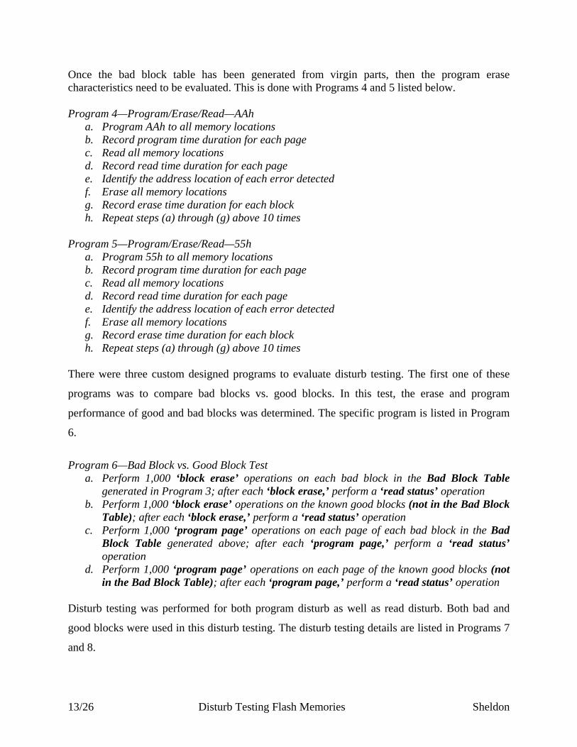
Bad Block Testing: Prior to testing the Micron 2Gb parts, recent historical data on the related
Micron 4Gb device was analyzed [Heidecker]. The 4Gb and 2Gb share the same data sheet, and
therefore, the same common technology and design practices. There was also a larger sample
size of 4Gb compared to the 2Gb (128 4Gb vs. 12 2Gb devices).
Approximately 14% of the 4Gb devices had zero bad blocks, and 25% of the 2Gb devices (3 out
of 12) had zero bad blocks. The 2Gb devices had a higher percentage (almost 2X) of bad blocks
when compared to the larger 4Gb device.
One would expect the opposite to be true in terms of number of defects. The 4Gb device is
roughly twice the size of the 2Gb, and therefore should have a 30%–40% reduction in the
number of good die using the standard Murphy yield formula [Stapper] of Y=e-AD where A is the
device area and D is the defect density. These data are shown in Figure 9 for the 4Gb devices and
Figure 10 for the 2G devices. Fourteen (14%) of the 4Gb devices have no bad blocks. Block size
on these devices is 64 pages or 128K + 4K bytes. The 4Gb device has 4,096 blocks. One bad
block represents approximately 0.02% of the die. Figure 9 represents a total of 128 4Gb devices
that were tested.
15/26 Disturb Testing Flash Memories Sheldon
Figure 9. Initial Number of Bad Blocks for 4G NAND
Figure 10. Initial Number of Bad Blocks for 2G NAND
Figure 9 shows that having one bad block is the highest populated category. This result is not
repeated in the 2Gb devices shown in Figure 10. For the 2Gb parts, the highest population
categories were either zero bad blocks or three bad blocks per device. The population curve
envelope that can be drawn over the 4Gb data in Figure 9 is indicative of either a skewed
Gaussian or perhaps a lognormal distribution. Given the sparse nature of the data in Figure 10,
no practical envelope can be drawn.
Micron MT29F4G08 NAND FLASH
0
5
10
15
20
25
30
35
0 1 2 3 4 5 6 7 8 9 10Quantity Of Bad Blocks Per Device
# of Bad Blocks - 2G NAND
0
0.5
1
1.5
2
2.5
3
3.5
0 1 2 3 4 5 6 7 8 9 10
# of Bad Blocks per Device
16/26 Disturb Testing Flash Memories Sheldon
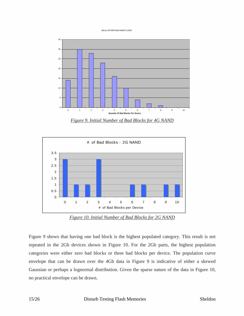
As the 2Gb devices were being prepared for the next test, the bad block information was double-
checked. During this testing, it was determined that none of the 12 devices had repeatable bad
block locations when compared to their initial bad block table (Table 2).
Table 2. Initial Bad Block Table
More of the bad blocks are in the lower logical addresses than the higher logical addresses.
Figure 11 illustrates the distribution of bad blocks by logical address. The smallest logical
address locations (0–500) show the highest number of bad blocks. The remaining frequency of
logical addresses is more or less uniformly distributed.
Figure 11. Frequency of Occurrence of Initial Bad Blocks by Logical Address
Device #1 242 347 775 1230 1652 3057 351123 235 604 711 1107 1206 1626 2563 3062 3077 347545 654 1430 26036 7 2025 346378 1502 27759 130 304 430 1311 1742 2444 3167 3624 372110 134 717 772 1771 2136 357011 325 2137 365612 156
Bad Block Location
Bad Block Location and Frequency
0.00
2.00
4.00
6.00
8.00
10.00
12.00
0-500 501-1000
1001-1500
1501-2000
2001-2500
2501-3000
3001-3500
3501-4000
Logical Block Addresses
17/26 Disturb Testing Flash Memories Sheldon
The failure of the bad block table to remain consistent and repeatable put the entire experimental
plan at risk. The main hypothesis to be proven or disproved was based on the assumption that a
bad block contained a hard error. This hard error site was to be exploited as a means to increase
the possibility of inducing a disturb failure in a nearby good site. The quality of the entire die is
now at question. To address this die quality issue, the following test sequence was developed and
implemented. This test sequence is designed to evaluate the data retention performance of the
devices to both logical states.
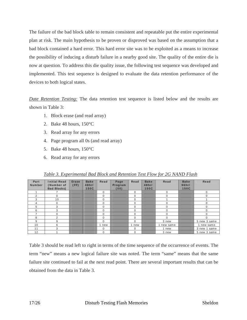
Date Retention Testing: The data retention test sequence is listed below and the results are
shown in Table 3:
1. Block erase (and read array)
2. Bake 48 hours, 150°C
3. Read array for any errors
4. Page program all 0s (and read array)
5. Bake 48 hours, 150°C
6. Read array for any errors
Table 3. Experimental Bad Block and Retention Test Flow for 2G NAND Flash Part
Number Initial Read (Number of Bad Blocks)
Erase (FF)
Bake 48hr/ 150C
Read Page Program
(00)
Read Bake 48hr/ 150C
Read Bake 96hr/ 150C
Read
1 7 0 0 0 0 2 0 0 0 0 0 3 10 0 0 1 1 4 0 0 0 0 0 5 3 0 0 0 0 6 3 0 0 0 0 7 0 0 0 0 0 8 2 0 0 0 0 9 9 0 0 3 new 5 new 3 same 10 6 1 new 1 new 1 new same 1 new same 11 3 0 0 1 new 3 new 1 same 12 1 0 0 3 new 5 new 3 same
Table 3 should be read left to right in terms of the time sequence of the occurrence of events. The
term “new” means a new logical failure site was noted. The term “same” means that the same
failure site continued to fail at the next read point. There are several important results that can be
obtained from the data in Table 3.
18/26 Disturb Testing Flash Memories Sheldon
1. The initial bad block information is totally non-repeatable after first erase and bake.
2. The initial number of bad blocks does not correlate to the number of retention failures
seen as a function of increasing time at temperature.
3. 33% of the population experienced retention failures while the remaining 66% did not
experience any retention failures during testing.
4. These data do not match Micron’s qualification and reliability data for the 2Gb device
[Micron Q&R]. Data retention bake results published in the Micron reference show 0
failures out of 237 parts baked at 150°C for up to 1008 hours. Micron reports this is
an equivalent FIT rate of 24 FITS at 50°C. The 33% failures in 192 hours of testing
reported in this paper are an equivalent of 2,621 FITs at 50°C. This is a 100X larger
FIT rate than the standard parts listed in the Micron Q&R documents.
5. These data retention failures appear to be hard failures.
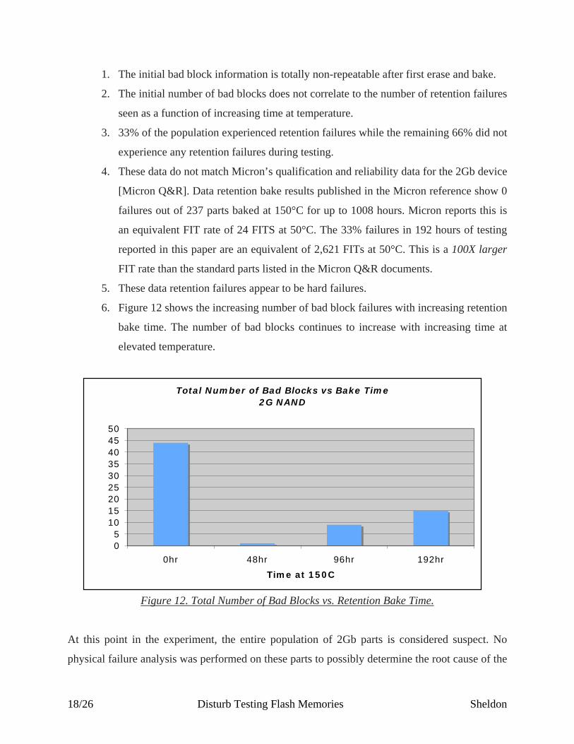
6. Figure 12 shows the increasing number of bad block failures with increasing retention
bake time. The number of bad blocks continues to increase with increasing time at
elevated temperature.
Figure 12. Total Number of Bad Blocks vs. Retention Bake Time.
At this point in the experiment, the entire population of 2Gb parts is considered suspect. No
physical failure analysis was performed on these parts to possibly determine the root cause of the
Total Number of Bad Blocks vs Bake Time2G NAND
05
101520253035404550
0hr 48hr 96hr 192hr
Time at 150C
19/26 Disturb Testing Flash Memories Sheldon
data retention failures. One possible suggestion to explain the results is that the parts may have
either missed entirely or only received a partial final burn-in and test by the manufacturer. The
parts were subjected to continued electrical testing to fully characterize their electrical
performance. This includes voltage corner testing as well as the originally designed disturb
testing. Voltage corner testing was performed on all parts as means to try to understand the
retention and bad block results.
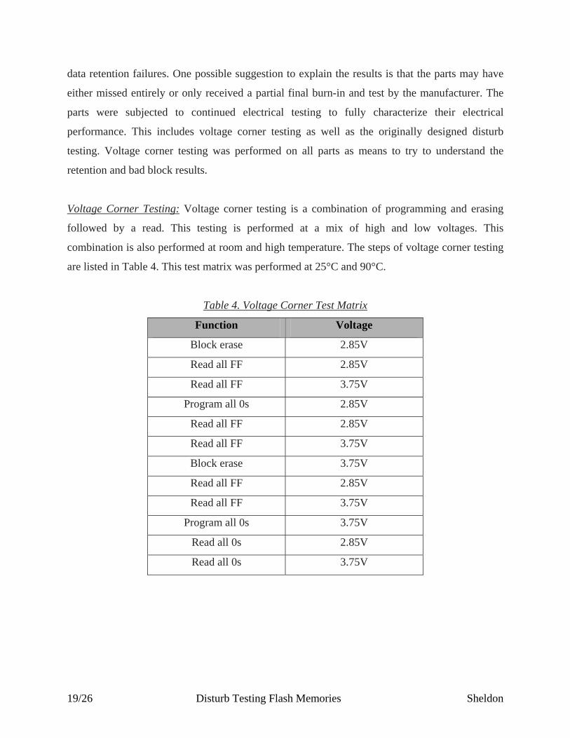
Voltage Corner Testing: Voltage corner testing is a combination of programming and erasing
followed by a read. This testing is performed at a mix of high and low voltages. This
combination is also performed at room and high temperature. The steps of voltage corner testing
are listed in Table 4. This test matrix was performed at 25°C and 90°C.
Table 4. Voltage Corner Test Matrix
Function Voltage
Block erase 2.85V
Read all FF 2.85V
Read all FF 3.75V
Program all 0s 2.85V
Read all FF 2.85V
Read all FF 3.75V
Block erase 3.75V
Read all FF 2.85V
Read all FF 3.75V
Program all 0s 3.75V
Read all 0s 2.85V
Read all 0s 3.75V
20/26 Disturb Testing Flash Memories Sheldon
Both device 3 and device 10 each had one bit location fail the read 0s testing at all voltages.
These bits failed at both 25°C and 90°C tests. All other devices passed. The failing bit locations
were the same locations that had failed in the previously discussed retention and bad block
experiments. These sites are stuck-at-1 faults. This means the erase command is not completely
removing all the charge on the floating gate of the failing cells.
The disturb testing was divided into program disturb and read disturb. A program disturb occurs
when one or more bits not intended to be programmed are changed from a “1” to a “0” during a
program operation. Increasing the number of partial page program operations has been shown to
exacerbate these types of errors [Micron Flash Application]. Program disturb errors can show up
on pages being programmed or on other pages within the same block.
Read disturb errors occur when one or more bits are changed from “1” to “0” during a read
operation. Read disturb errors occur within the block being read, but on a page or pages other
than the particular page being read. Performing a high number of read operations can increase
the possibility of read disturb errors. The number of read operations needs to be quite large
however. As listed in Program 8, page read operations were 50K, 100K, 500K, and 1M
operations on a single page.
No program disturb or read disturb failures where detected.
Conclusions
This experiment was designed to evaluate disturb errors on 2Gb NAND Flash devices. No
disturb errors were measured. However, the devices showed inconsistent bad block performance
and retention behavior. This behavior is concerning and could possibly adversely impact
reliability performance of these devices. It is recommended that all COTS flash devices targeted
for NASA missions be individually screened and characterized before being accepted for use.
21/26 Disturb Testing Flash Memories Sheldon
References Sheldon, D., “Integrated Qualification Strategies for FPGAs,” Microelectronics Reliability and
Quality Workshop, MRQW 2005, December 2005. Cooke, J., “Flash Memory Technology Direction,” Micron Applications Engineering Document,
May 2007. Heidecker, J., Internal JPL e-mail, September 2007. IEEE 10005-1998, “IEEE Standard Definitions and Characterization of Floating Gate
Semiconductor Arrays,” June 1998. Irom, F., and Nguyen, D., “Single Event Effect Characterization of High Density Commercial
NAND and NOR Nonvolatile Flash Memories,” Nuclear and Space Radiation Effects Conference, 2007.
Micron Flash Application TN-29-17, “Design and Use Considerations for NAND Flash
Memory,” Rev. A, August 2006. Micron Q&R, “Micron Internal Qualification and Reliability Report NAND Flash 2Gb 256 Meg
x 8, 3.3V,” M49A BOI, Rev. B, May 2006. Semiconductor Solutions, Inc., 2002, http://www.semiconductorsolutions.com/ Stapper, C.H., “On Murphy’s yield integral [IC Manufacture],” IEEE Transactions on
Semiconductor Manufacturing, Vol. 4, Issue 4, November 1991. Tanduo, P., Cola, L., Testa, S., Menchise, M, and Mervic, A., “Read Disturb in Flash Memories:
Reliability Case,” Microelectronics and Reliability, Vol. 46, Issues 9–11, pp. 1439–1444, September–November 2006.
Yang, H., Kim, H., Park, S., Kim, J., Lee, S.-H., Choi, J.-K., Hwang, D., Kim, C., Park, M., Lee,
K.-H., Park, Y.-K., Shin, J.K., and Kong, J.-T., “Reliability Issues and Models of sub-90nm NAND Flash Memory Cells,” 8th International Conference on Solid-State and Integrated Circuit Technology, pp. 760–762, October 2006.