Embed Size (px)
Citation preview

WWW.MOTOROLA.COM/SEMICONDUCTORS
DL200/DRev. 5, 01/2003
SensorDevice Data Book

ii
DATA CLASSIFICATIONProduct Preview
This heading on a data sheet indicates that the device is in the formative stages or in design (under development).The disclaimer at the bottom of the first page reads: “This document contains information on a product under develop-ment. Motorola reserves the right to change or discontinue this product without notice.”
Advance or Preliminary Information
This heading on a data sheet indicates that the device is in sampling, preproduction, or first production stages. Thedisclaimer at the bottom of the first page reads: “This document contains information on a new product. Specificationsand information herein are subject to change without notice.”
Fully Released
A fully released data sheet contains neither a classification heading nor a disclaimer at the bottom of the first page.This document contains information on a product in full production. Guaranteed limits will not be changed withoutwritten notice to your local Motorola Semiconductor Sales Office.
MOTOROLA DEVICE CLASSIFICATIONS
In an effort to provide up-to-date information to the customer regarding the status of any given device, Motorola hasclassified all devices into three categories: Preferred devices, Current products and Not Recommended for NewDesign products.
A Preferred type is a device which is recommended as a first choice for future use. These devices are “preferred”by virtue of their performance, price, functionality, or combination of attributes which offer the overall “best” value tothe customer. This category contains both advanced and mature devices which will remain available for the fore-seeable future.
Preferred devices in the Data Sheet sections areidentified as a “Motorola Preferred Device.’’
Device types identified as “current” may not be a first choice for new designs, but will continue to be availablebecause of the popularity and/or standardization or volume usage in current production designs. These products canbe acceptable for new designs but the preferred types are considered better alternatives for long term usage.
Any device that has not been identified as a “preferred device” is a “current” device.
Products designated as “Not Recommended for New Design” may become obsolete as dictated by poor marketacceptance, or a technology or package that is reaching the end of its life cycle. Devices in this category have anuncertain future and do not represent a good selection for new device designs or long term usage.
The Sensor Data Book does not contain any“Not Recommended for New Design” devices.

iii
Device Data Book
The information in this book has been carefully reviewed and is believed to be accurate; however, no responsibilityis assumed for inaccuracies. Furthermore, this information does not convey to the purchaser of semiconductordevices any license under the patent rights to the manufacturer.
Motorola reserves the right to make changes without further notice to any products herein. Motorola makes no war-ranty, representation, or guarantee regarding the suitability of its products for any particular purpose, nor does Motoro-la assume any liability arising out of the application or use of any product or circuit, and specifically disclaims any andall liability, including without limitation consequential or incidental damages. “Typical” parameters can and do vary indifferent applications and actual performance may vary over time. All operating parameters, including “Typicals”, mustbe validated for each customer application by customer’s technical experts. Motorola does not convey any licenseunder its patent rights nor the rights of others. Motorola products are not designed, intended, or authorized for useas components in systems intended for surgical implant into the body, or other applications intended to support orsustain life, or for any other application in which the failure of the Motorola product could create a situation wherepersonal injury or death may occur. Should Buyer purchase or use Motorola products for any such unintended or un-authorized application, Buyer shall indemnify and hold Motorola and its officers, employees, subsidiaries, affiliates,and distributors harmless against all claims, costs, damages, and expenses, and reasonable attorney fees arisingout of, directly or indirectly, any claim of personal injury or death associated with such unintended or unauthorizeduse, even if such claim alleges that Motorola was negligent regarding the design or manufacture of the part. Motorolaand the Stylized M Logo are registered in the US Patent & Trademark Office. All other product or service names arethe property of their respective owners. Motorola, Inc. is an Equal Opportunity/Affirmative Action Employer.
5th Edition Motorola, Inc. 2003“All Rights Reserved” Printed in U.S.A.

iv

v
TABLE OF CONTENTS
SECTION ONE — General Information
Quality and Reliability 1–2. . . . . . . . . . . . . . . . . . . . . . . . . . . Overview 1–2. . . . . . . . . . . . . . . . . . . . . . . . . . . . . . . . . . . . . . Reliability Issues for Silicon Pressure Sensors 1–3. . . . . . Soldering Precautions 1–10. . . . . . . . . . . . . . . . . . . . . . . . . . Pressure Sensors 1–11. . . . . . . . . . . . . . . . . . . . . . . . . . . . .
Electrostatic Process Control 1–17. . . . . . . . . . . . . . . . . . Statistical Process Control 1–11. . . . . . . . . . . . . . . . . . . . . .
Test Results 1–17. . . . . . . . . . . . . . . . . . . . . . . . . . . . . . . . . . . Accelerometer 1–17. . . . . . . . . . . . . . . . . . . . . . . . . . . . . . . .
Media Compatibility Overview 1–18. . . . . . . . . . . . . . . . . . .
SECTION TWO — Acceleration Sensor Products
Mini Selector Guide 2–2. . . . . . . . . . . . . . . . . . . . . . . . . . . . .
Device Numbering System 2–2. . . . . . . . . . . . . . . . . . . . . . .
Sensor Applications 2–3. . . . . . . . . . . . . . . . . . . . . . . . . . . . .
Acceleration Sensor FAQ’s 2–4. . . . . . . . . . . . . . . . . . . . . . .
Data SheetsMMA1200D 2– 5. . . . . . . . . . . . . . . . . . . . . . . . . . . . . . . . . . . MMA1201P 2–12. . . . . . . . . . . . . . . . . . . . . . . . . . . . . . . . . . . MMA1220D 2– 18. . . . . . . . . . . . . . . . . . . . . . . . . . . . . . . . . . MMA1250D 2–24. . . . . . . . . . . . . . . . . . . . . . . . . . . . . . . . . . . MMA1260D 2–30. . . . . . . . . . . . . . . . . . . . . . . . . . . . . . . . . . . MMA1270D 2–36. . . . . . . . . . . . . . . . . . . . . . . . . . . . . . . . . . . MMA2201D 2– 42. . . . . . . . . . . . . . . . . . . . . . . . . . . . . . . . . . MMA2202D 2– 48. . . . . . . . . . . . . . . . . . . . . . . . . . . . . . . . . . MMA3201D 2– 55. . . . . . . . . . . . . . . . . . . . . . . . . . . . . . . . . .
Application NotesAN1559 Application Considerations for a Switched
Capacitor Accelerometer 2– 62. . . . . . . . . . . . . AN1611 Impact and Tilt Measurement
Using Accelerometer 2–65. . . . . . . . . . . . . . . . . . AN1612 Shock and Mute Pager Applications
Using Accelerometer 2–77. . . . . . . . . . . . . . . . . . AN1632 MMA1201P Product Overview
and Interface Considerations 2– 84. . . . . . . . . . AN1635 Baseball Pitch Speedometer 2– 89. . . . . . . . . . . . AN1640 Reducing Accelerometer
Susceptibility to BCI 2–101. . . . . . . . . . . . . . . . . AN1925 Using the Motorola Accelerometer
Evaluation Board 2– 104. . . . . . . . . . . . . . . . . . .
Case Outlines 2–107. . . . . . . . . . . . . . . . . . . . . . . . . . . . . . . . .
Glossary of Terms 2–109. . . . . . . . . . . . . . . . . . . . . . . . . . . . .
SECTION THREE — Pressure Sensor Products
Mini Selector Guide 3–2. . . . . . . . . . . . . . . . . . . . . . . . . . . . .
Device Numbering System 3–4. . . . . . . . . . . . . . . . . . . . . . .
Package Offerings 3–5. . . . . . . . . . . . . . . . . . . . . . . . . . . . . . .
Orderable Part Numbers 3–6. . . . . . . . . . . . . . . . . . . . . . . . .
Pressure Sensor OverviewGeneral Information 3–7. . . . . . . . . . . . . . . . . . . . . . . . . . . . . Motorola Pressure Sensors 3–8. . . . . . . . . . . . . . . . . . . . . . Integration 3–12. . . . . . . . . . . . . . . . . . . . . . . . . . . . . . . . . . . . Sensor Applications 3–13. . . . . . . . . . . . . . . . . . . . . . . . . . . Pressure Sensor FAQ’s 3–14. . . . . . . . . . . . . . . . . . . . . . . .
Data SheetsMPX10, MPXV10GC Series 3–15. . . . . . . . . . . . . . . . . . . . MPX12 Series 3–19. . . . . . . . . . . . . . . . . . . . . . . . . . . . . . . . MPX2010, MPXV2010G Series 3–23. . . . . . . . . . . . . . . . . MPX2050 Series 3–27. . . . . . . . . . . . . . . . . . . . . . . . . . . . . . MPX2053, MPXV2053G Series 3–31. . . . . . . . . . . . . . . . . MPX2100 Series 3–35. . . . . . . . . . . . . . . . . . . . . . . . . . . . . . MPX2102, MPXV2102G Series 3–39. . . . . . . . . . . . . . . . . MPX2200 Series 3–43. . . . . . . . . . . . . . . . . . . . . . . . . . . . . . MPX2202, MPXV2202G Series 3–47. . . . . . . . . . . . . . . . . MPX2300DT1, MPX2301DT1 3–51. . . . . . . . . . . . . . . . . . . MPX4080D 3–54. . . . . . . . . . . . . . . . . . . . . . . . . . . . . . . . . . . MPX4100 Series 3–59. . . . . . . . . . . . . . . . . . . . . . . . . . . . . . MPX4100A, MPXA4100A Series 3–64. . . . . . . . . . . . . . . . MPX4101A MPXA4101A, MPXH6101A Series 3–70. . . . MPX4105A Series 3–75. . . . . . . . . . . . . . . . . . . . . . . . . . . . . MPX4115A, MPXA4115A Series 3–79. . . . . . . . . . . . . . . . . MPX4200A Series 3–84. . . . . . . . . . . . . . . . . . . . . . . . . . . . . MPX4250A, MPXA4250A Series 3–88. . . . . . . . . . . . . . . . MPX4250D Series 3–93. . . . . . . . . . . . . . . . . . . . . . . . . . . . . MPX5010, MPXV5010G Series 3–97. . . . . . . . . . . . . . . . . MPX5050, MPXV5050G Series 3–103. . . . . . . . . . . . . . . . MPX5100 Series 3–108. . . . . . . . . . . . . . . . . . . . . . . . . . . . . MPX53, MPXV53GC Series 3–114. . . . . . . . . . . . . . . . . . . MPX5500 Series 3–118. . . . . . . . . . . . . . . . . . . . . . . . . . . . . MPX5700 Series 3–122. . . . . . . . . . . . . . . . . . . . . . . . . . . . . MPX5999D 3–126. . . . . . . . . . . . . . . . . . . . . . . . . . . . . . . . . . MPXA6115A, MPXH6115A 3–130. . . . . . . . . . . . . . . . . . . . MPXAZ4100A Series 3–135. . . . . . . . . . . . . . . . . . . . . . . . . MPXAZ4115A Series 3–140. . . . . . . . . . . . . . . . . . . . . . . . . MPXAZ6115A Series 3–145. . . . . . . . . . . . . . . . . . . . . . . . . MPXC2011DT1, MPXC2012DT1 3–150. . . . . . . . . . . . . . . MPXH6300A Series 3–153. . . . . . . . . . . . . . . . . . . . . . . . . . MPXM2010 Series 3–158. . . . . . . . . . . . . . . . . . . . . . . . . . . MPXM2053 Series 3–161. . . . . . . . . . . . . . . . . . . . . . . . . . . MPXM2102 Series 3–164. . . . . . . . . . . . . . . . . . . . . . . . . . . MPXM2202 Series 3–167. . . . . . . . . . . . . . . . . . . . . . . . . . . MPXV4006G Series 3–170. . . . . . . . . . . . . . . . . . . . . . . . . . MPXV4115V Series 3–174. . . . . . . . . . . . . . . . . . . . . . . . . . . MPXV5004G Series 3–179. . . . . . . . . . . . . . . . . . . . . . . . . . MPXV6115VC6U 3–183. . . . . . . . . . . . . . . . . . . . . . . . . . . . .
Application NotesAN935 Compensating for Nonlinearity in the
MPX10 Series Pressure Transducer 3–188. . . AN936 Mounting Techniques, Lead Forming
and Testing of Motorola’s MPX SeriesMPX10 Series Pressure Sensors 3–195. . . . . .
AN1082 Simple Design for a 3–20 mA TransmitterInterface Using a Motorola Pressure Sensor 3–200. . . . . . . . . . . . . . . . . . . .
(continued — next page)

vi
Table of Contents (continued)
SECTION THREE (continued)
AN1097 Calibration–Free PressureSensor System 3–203. . . . . . . . . . . . . . . . . . . . . .
AN1100 Analog to Digital Converter ResolutionExtension Using a MotorolaPressure Sensor 3–208. . . . . . . . . . . . . . . . . . . .
AN1303 A Simple 3–20 mA PressureTransducer Evaluation Board 3–211. . . . . . . . .
AN1304 Integrated Sensor Simplifies BarGraph Pressure Gauge 3–214. . . . . . . . . . . . . . .
AN1305 An Evaluation System for DirectInterface of the MPX5100 PressureSensor with a Microprocessor 3–219. . . . . . . . .
AN1309 Compensated Sensor Bar GraphPressure Gauge 3–235. . . . . . . . . . . . . . . . . . . . .
AN1315 An Evaluation System Interfacing theMPX2000 Series Pressure Sensorsto a Microprocessor 3–242. . . . . . . . . . . . . . . . . .
AN1316 Frequency Output Conversion forMPX2000 Series Pressure Sensors 3–263. . . .
AN1318 Interfacing Semiconductor PressureSensors to Microcomputers 3–269. . . . . . . . . . .
AN1322 Applying Semiconductor Sensors toBar Graph Pressure Gauges 3–279. . . . . . . . . .
AN1325 Amplifiers for SemiconductorPressure Sensors 3–284. . . . . . . . . . . . . . . . . . .
AN1326 Barometric Pressure MeasurementUsing SemiconductorPressure Sensors 3–288. . . . . . . . . . . . . . . . . . .
AN1513 Mounting Techniques and PlumbingOptions of Motorola’s MPX SeriesPressure Sensors 3–297. . . . . . . . . . . . . . . . . . .
AN1516 Liquid Level Control Using aMotorola Pressure Sensor 3–301. . . . . . . . . . . .
AN1517 Pressure Switch Design withSemiconductor Pressure Sensors 3–306. . . . .
AN1518 Using a Pulse Width ModulatedOutput with SemiconductorPressure Sensors 3–312. . . . . . . . . . . . . . . . . . .
AN1525 The A–B–C’s of Signal–ConditioningAmplifier Design forSensor Applications 3–318. . . . . . . . . . . . . . . . . .
AN1536 Digital Boat Speedometers 3–325. . . . . . . . . . . . . AN1551 Low Pressure Sensing with the
MPX2010 Pressure Sensor 3–337. . . . . . . . . . . AN1556 Designing Sensor Performance
Specifications forMCU–based Systems 3–346. . . . . . . . . . . . . . . .
AN1571 Digital Blood Pressure Meter 3–355. . . . . . . . . . . .
AN1573 Understanding Pressure and Pressure Measurement 3–363. . . . . . . . . . .
AN1586 Designing a Homemade Digital Outputfor Analog Voltage Output Sensors 3–368. . . . .
AN1636 Implementing Auto Zero forIntegrated Pressure Sensors 3–375. . . . . . . . . .
AN1646 Noise Considerations for IntegratedPressure Sensors 3–378. . . . . . . . . . . . . . . . . . .
AN1660 Compound Coefficient Pressure SensorPSPICE Models 3–384. . . . . . . . . . . . . . . . . . . . .
AN1668 Washing Appliance Sensor Selection 3–390. . . . . AN1950 Water Level Monitoring 3–395. . . . . . . . . . . . . . . . . AN4007 New Small Amplified Automotive
Vacuum SensorsA Single Chip Sensor Solutionfor Brake Booster Monitoring 3–413. . . . . . . . . .
AN4010 Low–Pressure Sensing Using MPX2010 Series Pressure Sensors 3–418. . . .
Case Outlines 3–423. . . . . . . . . . . . . . . . . . . . . . . . . . . . . . . . .
Reference InformationReference Tables 3–439. . . . . . . . . . . . . . . . . . . . . . . . . . . . . Mounting and Handling Suggestions 3–441. . . . . . . . . . . . Standard Warranty Clause 3–442. . . . . . . . . . . . . . . . . . . . .
Glossary of Terms 3–443. . . . . . . . . . . . . . . . . . . . . . . . . . . . .
Symbols, Terms, and Definitions 3–446. . . . . . . . . . . . . . .
SECTION FOUR — Safety and Alarm IntegratedCircuits
Mini Selector Guide 4–2. . . . . . . . . . . . . . . . . . . . . . . . . . . . .
Data SheetsMC14467–1 4– 3. . . . . . . . . . . . . . . . . . . . . . . . . . . . . . . . . . MC14468 4– 9. . . . . . . . . . . . . . . . . . . . . . . . . . . . . . . . . . . . MC14578 4– 15. . . . . . . . . . . . . . . . . . . . . . . . . . . . . . . . . . . MC14600 4–19. . . . . . . . . . . . . . . . . . . . . . . . . . . . . . . . . . . . MC145010 4– 24. . . . . . . . . . . . . . . . . . . . . . . . . . . . . . . . . . MC145011 4– 34. . . . . . . . . . . . . . . . . . . . . . . . . . . . . . . . . . MC145012 4– 44. . . . . . . . . . . . . . . . . . . . . . . . . . . . . . . . . . MC145017 4–54. . . . . . . . . . . . . . . . . . . . . . . . . . . . . . . . . . . MC145018 4– 60. . . . . . . . . . . . . . . . . . . . . . . . . . . . . . . . . .
Application NotesAN1690 Alarm IC General Applications
Overview 4– 66. . . . . . . . . . . . . . . . . . . . . . . . . . . AN4009 Alarm IC Sample Applications 4–70. . . . . . . . . . . .
Case Outlines 4–72. . . . . . . . . . . . . . . . . . . . . . . . . . . . . . . . . .
SECTION FIVE — Alphanumeric Device Index
Alphanumeric Device Index 5–2. . . . . . . . . . . . . . . . . . . . . .

1–1Motorola Sensor Device Data www.motorola.com/semiconductors
Section One
Introduction:This version of the Sensor Products Device Data Hand-
book is organized to provide easy reference to sensor deviceinformation. We have reorganized the book based upon yourrecommendations with our goal to make designing in pres-sure, acceleration and safety and alarm ICs easy, and if youdo have a question, you will have access to the technicalsupport you need.
The handbook is organized by product line, acceleration,pressure and safety and alarm ICs. Once in a section, youwill find a glossary of terms, a list of frequently asked ques-tions or other relevant data. If you have recommendations forimprovement, please complete the comment card and returnit to us or, feel free to call our Sensor Device Data Handbookhot line and we will personally record your comments. Thehot line number is 480/413–3333. We look forward to hear-ing from you!
Quality and Reliability 1–2. . . . . . . . . . . . . . . . . . . . . . .
Overview 1–2. . . . . . . . . . . . . . . . . . . . . . . . . . . . . . . . . . . .
Reliability Issues for Silicon Pressure Sensors 1–3. . . .
Soldering Precautions 1–10. . . . . . . . . . . . . . . . . . . . . . . .
Pressure Sensors 1–11. . . . . . . . . . . . . . . . . . . . . . . . . . .
Electrostatic Process Control 1–11. . . . . . . . . . . . . . . .
Statistical Process Control 1–13. . . . . . . . . . . . . . . . . . . .
Test Results 1–17. . . . . . . . . . . . . . . . . . . . . . . . . . . . . . . .
Accelerometer 1–17. . . . . . . . . . . . . . . . . . . . . . . . . . . . . .
Media Compatability Overview 1–18. . . . . . . . . . . . .

1–2 Motorola Sensor Device Datawww.motorola.com/semiconductors
Quality and Reliability — OverviewA Major Objective of the Production Cycle
From rigid incoming inspection of piece parts and materials,to stringent outgoing quality verification, the Motorolaassembly and process flow is encompassed by an elaboratesystem of test and inspection stations; stations to ensure astep-by-step adherence to prescribed procedure. Thisproduces the high level of quality for which Motorola isknown . . . from start to finish.
As illustrated in the process flow overview, every majormanufacturing step is followed by an appropriate in-process
quality inspection to insure product conformance tospecification. In addition, Statistical Process Control (S.P.C.)techniques are utilized on all critical processes to insureprocessing equipment is capable of producing the product tothe target specification while minimizing the variability.Quality control in wafer processing, assembly, and final testimpart Motorola sensor products with a level of reliability thateasily exceeds almost all industrial, consumer, and militaryrequirements.
Compensated Sensor Flow Chart
LASER I.D.BINNINGCHECK
INITIALOXIDATION
P+ PHOTORESIST
P+DIFFUSION
RESISTORPHOTORESIST
CAVITYPHOTORESIST
DIE SORTAND LOAD
GEL FILLAND CURE
RESISTORIMPLANT
THIN-FILMMETAL DEP.
WAFERFINAL
VISUAL
CELLMARKING
100%FUNCTIONAL
TEST
EMITTERPHOTORESIST
THIN-FILMMETAL P.R.
CLASSPROBE
DIE BONDAND CURE
FINALVISUAL
EMITTERDIFFUSION
CONTACTPHOTORESIST
WAFERTO WAFER
BOND
WIREBOND
PACK ANDSHIP
FINALOXIDATION
FRONTMETAL
1 2 3 4
5 6 7 9
10 11
13 15 16
17 18 19
20 21 22 23
8
METALPHOTORESIST
12
CAVITYETCH
14
SAW ANDWASH
LASERTRIM
1–3Motorola Sensor Device Data www.motorola.com/semiconductors
Reliability Issues for Silicon Pressure Sensors
by Theresa Maudie and Bob TuckerSensor Products DivisionRevised June 9, 1997
ABSTRACTReliability testing for silicon pressure sensors is of
greater importance than ever before with the dramaticincrease in sensor usage. This growth is seen in applica-tions replacing mechanical systems, as well as newdesigns. Across all market segments, the expectation forthe highest reliability exists. While sensor demand hasgrown across all of these segments, the substantial increaseof sensing applications in the automotive arena is drivingthe need for improved reliability and test capability. Thepurpose of this paper is to take a closer look at these reli-ability issues for silicon pressure sensors.
INTRODUCTIONDiscussing reliability as it pertains to semiconductor elec-
tronics is certainly not a new subject. However, when devel-oping new technologies like sensors how reliability testingwill be performed is not always obvious. Pressure sensorsare an intriguing dilemma. Since they are electromechanicaldevices, different types of stresses should be considered toinsure the different elements are exercised as they would bein an actual application. In addition, the very differentpackage outlines relative to other standard semiconductorpackages require special fixtures and test set-ups. However,as the sensor marketplace continues to grow, reliabilitytesting becomes more important than ever to insure thatproducts being used across all market segments will meetreliability lifetime expectations.
RELIABILITY DEFINITIONReliability is [1] the probability of a product performing its
intended function over its intended lifetime and under theoperating conditions encountered. The four key elements ofthe definition are probability, performance, lifetime, andoperating conditions. Probability implies that the reliabilitylifetime estimates will be made based on statistical tech-niques where samples are tested to predict the lifetime ofthe manufactured products. Performance is a key in that thesample predicts the performance of the product at a givenpoint in time but the variability in manufacturing must becontrolled so that all devices perform to the same functionallevel. Lifetime is the period of time over which the product isintended to perform. This lifetime could be as small as oneweek in the case of a disposable blood pressure transduceror as long as 15 years for automotive applications. Environ-ment is the area that also plays a key role since the oper-ating conditions of the product can greatly influence thereliability of the product.
Environmental factors that can be seen during the lifetimeof any semiconductor product include temperature, humidity,electric field, magnetic field, current density, pressure differ-ential, vibration, and/or a chemical interaction. Reliabilitytesting is generally formulated to take into account all ofthese potential factors either individually or in multiple
combinations. Once the testing has been completed predic-tions can be made for the intended product customer base.
If a failure would be detected during reliability testing, thecause of the failure can be categorized into one of thefollowing: design, manufacturing, materials, or user. Thepossible impact on the improvements that may need to bemade for a product is influenced by the stage of productdevelopment. If a product undergoes reliability testing earlyin its development phase, the corrective action process cangenerally occur in an expedient manner and at minimumcost. This would be true whether the cause of failure wasattributed to the design, manufacturing, or materials. If areliability failure is detected once the product is in fullproduction, changes can be very difficult to make andgenerally are very costly. This scenario would sometimesresult in a total redesign.
The potential cause for a reliability failure can also beuser induced. This is generally the area that the leastinformation is known, especially for a commodity typemanufacturer that achieves sales through a global distribu-tion network. It is the task of the reliability engineer to bestanticipate the multitudes of environments that a particularproduct might see, and determine the robustness of theproduct by measuring the reliability lifetime parameters.The areas of design, manufacturing, and materials aregenerally well understood by the reliability engineer, butwithout the correct environmental usage, customer satis-faction can suffer from lack of optimization.
RELIABILITY STATISTICSWithout standardization of the semiconductor sensor stan-
dards, the end customer is placed in a situation of possiblejeopardy. If non-standard reliability data is generated andpublished by manufacturers, the information can beperplexing to disseminate and compare. Reliability lifetimestatistics can be confusing for the novice user of the informa-tion, “let the buyer beware”.
The reporting of reliability statistics is generally in terms offailure rate, measured in FITs, or failure rate for one billiondevice hours. In most cases, the underlying assumptionused in reporting either the failure rate or the MTBF is thatthe failures occurring during the reliability test follow an expo-nential life distribution. The inverse of the failure rate is theMTBF, or mean time between failure. The details on thevarious life distributions will not be explored here but the keyconcern about the exponential distribution is that the failurerate over time is constant. Other life distributions, such as thelognormal or Weibull can take on different failure rates overtime, in particular, both distributions can represent a wear outor increasing failure rate that might be seen on a productreaching the limitations on its lifetime or for certain types offailure mechanisms.
The time duration use for the prediction of most reliabilitystatistics is of relatively short duration with respect to theproduct’s lifetime ability and failures are usually notobserved. When a test is terminated after a set number ofhours is achieved, or time censored, and no failures areobserved, the failure rate can be estimated by use of the chi-square distribution which relates observed and expected

1–4 Motorola Sensor Device Datawww.motorola.com/semiconductors
frequencies of an event to established confidence intervals.The relationship between failure rate and the chi-squaredistribution is as follows:
L1 2 , d.f.
2t
Where:
λ = failure rateL1 = lower one side confidence limitχ2 = chi–square functionα = risk, (1–confidence level)
d.f. = degrees of freedom = 2 (r + 1)r = number of failurest = device hours
Chi-square values for 60% and 90% confidence intervalsfor up to 12 failures is shown in Table 1.
As indicated by the table, when no failures occur, anestimate for the chi-square distribution interval is obtainable.This interval estimate can then be used to solve for thefailure rate, as shown in the equation above. If no failuresoccur, the failure rate estimate is solely a function of theaccumulated device hours. This estimate can vary dramati-cally as additional device hours are accumulated.
As a means of showing the influence of device hours withno failures on the failure rate value, a graphical representa-tion of cumulative device hours versus the failure ratemeasured in FITs is shown in Figure 1.
A descriptive example between two potential vendors bestserves to demonstrate the point. If vendor A is introducing a
new product and they have put a total of 1,000 parts on ahigh temperature storage test for 500 hours each, theircorresponding cumulative device hours would be 500,000device hours. Vendor B has been in the business for severalyears on the same product and has tested a total of 500,000parts for 10 hours each to the same conditions as part of anin-line burn-in test for a total of 5,000,000 device hours. Thecorresponding failure rate for a 60% confidence level forvendor A would be 1,833 FITs, vendor B would have a FITrate of 183 FITs.
Table 1. Chi-Square Table
Chi-Square Distribution Function
60% Confidence Level 90% Confidence Level
No. Fails χ2 Quantity No. Fails χ2 Quantity
0 1.833 0 4.605
1 4.045 1 7.779
2 6.211 2 10.645
3 8.351 3 13.362
4 10.473 4 15.987
5 12.584 5 18.549
6 14.685 6 21.064
7 16.780 7 23.542
8 18.868 8 25.989
9 20.951 9 28.412
10 23.031 10 30.813
11 25.106 11 33.196
12 27.179 12 35.563
CUMULATIVE DEVICE HOURS, [t]
105
108
107
109
104
100
10
1
0.1
1,000
106
1 10 100 1,000 104 105 106 107 108 109
FAIL
UR
E R
ATE,
[FIT
s]
Figure 1. Depiction of the influence on the cumulative device hours with no failuresand the Failure Rate as measured in FITs.

1–5Motorola Sensor Device Data www.motorola.com/semiconductors
One could thus imply that the reliability performanceindicates that vendor B has an order of magnitude improve-ment in performance over vendor A with neither one seeingan occurrence of failure during their performance.
The incorrect assumption of a constant failure rate overtime can potentially result in a less reliable device beingdesigned into an application. The reliability testing assump-tions and test methodology between the various vendorsneeds to be critiqued to insure a full understanding of theproduct performance over the intended lifetime, especially inthe case of a new product. Testing to failure and determina-tion of the lifetime statistics is beyond the scope of this paperand presented elsewhere [2].
INDUSTRY RELIABILITY STANDARDS
Reliability standards for large market segments are oftendeveloped by “cross-corporation” committees that evaluatethe requirements for the particular application of interest. It isthe role of these committees to generate documentsintended as guides for technical personnel of the end usersand suppliers, to assist with the following functions: speci-fying, developing, demonstrating, calibrating, and testing theperformance characteristics for the specific application.
One such committee which has developed a standard for aparticular application is the Blood Pressure MonitoringCommittee of the Association for the Advancement ofMedical Instrumentation (AAMI) [3]. Their document, the“American National Standard for Interchangeability andPerformance of Resistive Bridge Type Blood PressureTransducers”, has an objective to provide performancerequirements, test methodology, and terminology that willhelp insure that safe, accurate blood pressure transducersare supplied to the marketplace.
In the automotive arena, the Society of AutomotiveEngineers (SAE) develops standards for various pressuresensor applications such as SAE document J1346, “Guide toManifold Absolute Pressure Transducer Representative TestMethod” [4].
While these two very distinct groups have successfullydeveloped the requirements for their solid-state siliconpressure sensor needs, no real standard has been set for thegeneral industrial marketplace to insure products beingoffered have been tested to insure reliability under industrialconditions. Motorola has utilized MIL-STD-750 as a refer-ence document in establishing reliability testing practices forthe silicon pressure sensor, but the differences in thetechnology between a discrete semiconductor and a siliconpressure sensor varies dramatically. The additional tests thatare utilized in semiconductor sensor reliability testing arebased on the worst case operational conditions that thedevice might encounter in actual usage.
ESTABLISHED SENSOR TESTING
Motorola has established semiconductor sensor reliabilitytesting based on exercising to detect failures by thepresence of the environmental stress. Potential failuremodes and causes are developed by allowing tests to runbeyond the normal test times, thus stressing to destruction.The typical reliability test matrix used to insure conformanceto customers end usage is as follows [5]:
PULSED PRESSURE TEMPERATURE CYCLING WITHBIAS (PPTCB)
This test is an environmental stress test combined withcyclic pressure loading in which the devices are alternatelysubjected to a low and high temperature while operating underbias under a cyclical pressure load. This test simulates theextremes in the operational life of a pressure sensor. PPTCBevaluates the sensor’s overall performance as well asevaluating the die, die bond, wire bond and package integrity.
Typical Test Conditions: Temperature per specifiedoperating limits (i.e., Ta = –40 to 125°C for an automotiveapplication). Dwell time ≥ 15 minutes, transfer time ≤ 5minutes, bias = 100% rated voltage. Pressure = 0 to fullscale, pressure frequency = 0.05 Hz, test time = up to 1000hours.
Potential Failure Modes: Open, short, parametric shift.
Potential Failure Mechanisms: Die defects, wire bondfatigue, die bond fatigue, port adhesive failure, volumetricgel changes resulting in excessive package stress.Mechanical creep of packaging material.
HIGH HUMIDITY, HIGH TEMPERATURE WITH BIAS(H3TB)
A combined environmental/electrical stress test in whichdevices are subjected to an elevated ambient temperatureand humidity while under bias. The test is useful forevaluating package integrity as well as detecting surfacecontamination and processing flaws.
Typical Test Conditions: Temperature between 60 and85°C, relative humidity between 85 and 90%, rated voltage,test time = up to 1000 hours.
Potential Failure Modes: Open, short, parametric shift.
Potential Failure Mechanisms: Shift from ionic affect,parametric instability, moisture ingress resulting in exces-sive package stress, corrosion.
HIGH TEMPERATURE WITH BIAS (HTB)This operational test exposes the pressure sensor to a
high temperature ambient environment in which the device isbiased to the rated voltage. The test is useful for evaluatingthe integrity of the interfaces on the die and thin film stability.
Typical Test Conditions: Temperature per specifiedoperational maximum, bias = 100% rated voltage, test time= up to 1000 hours.
Potential Failure Modes: Parametric shift in offset and/orsensitivity.
Potential Failure Mechanisms: Bulk die or diffusiondefects, film stability and ionic contamination.
HIGH AND LOW TEMPERATURE STORAGE LIFE(HTSL, LTSL)
High and low temperature storage life testing is performedto simulate the potential shipping and storage conditions thatthe pressure sensor might encounter in actual usage. Thetest also evaluates the devices thermal integrity at worstcase temperatures.

1–6 Motorola Sensor Device Datawww.motorola.com/semiconductors
Typical Test Conditions: Temperature per specifiedstorage maximum and minimum, no bias, test time = up to1000 hours.
Potential Failure Modes: Parametric shift in offset and/orsensitivity.
Potential Failure Mechanisms: Bulk die or diffusiondefects, mechanical creep in packaging components due tothermal mismatch.
TEMPERATURE CYCLING (TC)This is an environmental test in which the pressure sensor
is alternatively subjected to hot and cold temperatureextremes with a short stabilization time at each temperaturein an air medium. The test will stress the devices bygenerating thermal mismatches between materials.
Typical Test Conditions: Temperature per specifiedstorage maximum and minimum (i.e., –40 to +125°C forautomotive applications). Dwell time ≥ 15 minutes, transfertime ≤ 5 minutes, no bias. Test time up to 1000 cycles.
Potential Failure Modes: Open, parametric shift in offsetand/or sensitivity.
Potential Failure Mechanisms: Wire bond fatigue, diebond fatigue, port adhesive failure, volumetric gel changesresulting in excessive package stress. Mechanical creep ofpackaging material.
MECHANICAL SHOCKThis is an environmental test where the sensor device is
evaluated to determine its ability to withstand a suddenchange in mechanical stress due to an abrupt change inmotion. This test simulates motion that may be seen inhandling, shipping or actual use. MIL STD 750, Method 2016Reference.
Typical Test Conditions: Acceleration = 1500 g’s, orienta-tion = X, Y, Z planes, time = 0.5 milliseconds, 5 blows.
Potential Failure Modes: Open, parametric shift in offsetand/or sensitivity.
Potential Failure Mechanisms: Diaphragm fracture,mechanical failure of wire bonds or package.
VARIABLE FREQUENCY VIBRATIONA test to examine the ability of the pressure sensor device
to withstand deterioration due to mechanical resonance. MILSTD 750, Method 2056 Reference.
Typical Test Conditions: Frequency – 10 Hz to 2 kHz, 6.0G’s max, orientation = X, Y, Z planes, 8 cycles each axis, 2hrs. per cycle.
Potential Failure Modes: Open, parametric shift in offsetand/or sensitivity.
Potential Failure Mechanisms: Diaphragm fracture,mechanical failure of wire bonds or package.
SOLDERABILITYIn this reliability test, the lead/terminals are evaluated for
their ability to solder after an extended time period of storage(shelf life). MIL STD 750, Method 2026 Reference.
Typical Test Conditions: Steam aging = 8 hours, Flux= R,Solder = Sn63, Pb37.
Potential Failure Modes: Pin holes, non–wetting,dewetting.
Potential Failure Mechanisms: Poor plating, contamination.
OVER PRESSUREThis test is performed to measure the ability of the
pressure sensor to withstand excessive pressures that maybe encountered in the application. The test is performed fromeither the front or back side depending on the application.
Typical Test Conditions: Pressure increase to failure,record value.
Potential Failure Modes: Open.
Potential Failure Mechanisms: Diaphragm fracture,adhesive or cohesive failure of die attach.
A pressure sensor may be placed in an application whereit will be exposed to various media that may chemicallyattack the active circuitry, silicon, interconnections and/orpackaging material. The focus of media compatibility is tounderstand the chemical impact with the other environmentalfactors such as temperature and bias and determine theimpact on the device lifetime. The primary driving mecha-nism to consider is permeation which quantifies the time for achemical to permeate across a membrane or encapsulantcorrosion can result.
Media related product testing is generally very specific tothe application since the factors that relate to the productlifetime are very numerous and varied. An example issolution pH where the further from neutral will drive thechemical reaction, generally to a power rule relationship. ThepH alone does not always drive the reaction either, thenon–desired products in the media such as strong acids infuels as a result of acid rain can directly influence the lifetime.It is recommended the customer and/or vendor performapplication specific testing that best represents the environ-ment. This testing should be performed utilizing in situmonitoring of the critical device parameter to insure thedevice survives while exposed to the chemical. The SensorProducts Division within Motorola has a wide range of mediaspecific test capabilities and under certain circumstances willperform application specific media testing.
A sufficient sample size manufactured over a pre-definedtime interval to maximize process and time variability istested based on the guidelines of the matrix shown above.This test methodology is employed on all new productintroductions and process changes on current products.
A silicon pressure sensor has a typical usage environ-ment of pressure, temperature, and voltage. Unlike thetypical bipolar transistor life tests which incorporate currentdensity and temperature to accelerate failures, a siliconpressure sensor’s acceleration of its lifetime performance isprimarily based on the pressure and temperature interac-tion with a presence of bias. This rationale was incorporatedinto the development of the Pulsed Pressure TemperatureCycling with Bias (PPTCB) test where the major accelera-tion factor is the pressure and temperature component. It isalso why PPTCB is considered the standard sensoroperational life test.

1–7Motorola Sensor Device Data www.motorola.com/semiconductors
To insure that silicon pressure sensors are designed andmanufactured for reliability, an in-depth insight into whatmechanisms cause particular failures is required. It is safe tosay that unless a manufacturer has a clear understanding ofeverything that can go wrong with the device, it cannotdesign a device for the highest reliability. Figure 2 provides alook into the sensor operating concerns for a variety ofpotential usage applications. This information is utilizedwhen developing the Failure Mode and Effects Analysis(FMEA). The FMEA then serves as the documentation thatdemonstrates all design and process concerns have beenaddressed to offer the most reliable approach. By under-standing how to design products, control processes, andeliminate the concerns raised, a reliable product is achieved.
ACCELERATED LIFE TESTINGIt is very difficult to assess the reliability statistics for a
product when very few or no failures occur. With cost as apredominant factor in any industrial setting and time of theutmost importance, the reliability test must be optimized.Optimization of reliability testing will allow the maximumamount of information on the product being tested to begained in a minimum amount of time, this is accomplished byusing accelerated life testing techniques.
A key underlying assumption in the usage of acceleratedlife testing to estimate the life of a product at a lower ornominal stress is that the failure mechanism encounteredat the high stress is the same as that encountered at thenominal stress. The most frequently applied acceleratedenvironmental stress for semiconductors is temperature, itwill be briefly explained here for its utilization in deter-mining the lifetime reliability statistics for silicon pressuresensors.
PACKAGE:IntegrityPlating QualityDimensionsThermal ResistanceMechanical ResistancePressure ResistanceMedia Compatibility
GEL:ViscosityThermal Coefficient of ExpansionPermeability (Diffusion x Solubility)Changes in Material or ProcessHeightCoverageUniformityAdhesive PropertiesMedia CompatibilityGel AerationCompressibility
DIEMETALLIZATION:Lifting or PeelingAlignmentScratchesVoidsLaser TrimmingThicknessStep CoverageContact Resistance Integrity
BONDING WIRES:StrengthPlacementHeight and LoopSizeMaterialBimetallic Contamination(Kirkendall Voids)Nicking and other damageGeneral Quality & Workmanship
DIAPHRAGM:SizeThicknessUniformityPitsAlignmentFracturePASSIVATION:ThicknessMechanical DefectsIntegrityUniformity
LEADS:Materials and FinishPlating IntegritySolderabilityGeneral QualityStrengthContaminationCorrosionAdhesion
ELECTRICAL PERFORMANCE:Continuity and ShortsParametric StabilityParametric PerformanceTemperature PerformanceTemperature StabilityLong Term ReliabilityStorage DegradationSusceptibility to Radiation DamageDesign Quality
DIE ATTACH:UniformityResistance to Mechanical StressResistance to Temperature StressWettingAdhesive StrengthCohesive StrengthProcess ControlsDie OrientationDie HeightChange in Material or ProcessMedia CompatibilityCompressibility
DESIGN CHANGESMATERIAL OR PROCESS CHANGESFAB & ASSEMBLY CLEANLINESSSURFACE CONTAMINATIONFOREIGN MATERIALSCRIBE DEFECTSDIFFUSION DEFECTSOXIDE DEFECTS
Figure 2. Process and Product Variability Concerns During Reliability Testing
ÉÉÉÉÉÉÉÉÉÉÉÉÉÉÉÉÉÉÉÉÉÉÉÉÉÉÉÉÉÉÉÉÉÉÉÉÉÉÉÉÉÉÉÉÉÉÉÉÉÉÉÉÉÉÉÉÉÉÉÉÉÉÉÉÉÉÉÉÉÉÉÉÉÉÉÉÉÉÉÉÉÉÉÉÉÉÉÉÉÉÉÉÉÉÉÉÉÉÉÉÉÉÉÉÉÉÉÉÉÉÉÉÉÉÉÉÉÉÉ
MARKING:PermanencyClarity
SENSOR RELIABILITY CONCERNS
ÄÄÄÄÄÄÄÄÄÄ

1–8 Motorola Sensor Device Datawww.motorola.com/semiconductors
The temperature acceleration factor for a particular failuremechanism can be related by taking the ratio for the reactionrate of the two different stress levels as expressed by theArrhenius type of equation. The mathematical derivation ofthe first order chemical reaction rate computes to:
AF (RT)HS
tHS
(RT)LS tLS
AF exp Eak 1TLS
1THS
Where:AF = Acceleration FactorRT = Reaction Ratet = timeT = temperature [°K]Ea = activation energy of expressed
in electron-volts [eV]k = Boltzman’s constant, 8.6171 x 10⁻⁵ eV/°KLS = Low stress or nominal temperatureHS = High stress or test temperature
The activation energy is dependent on the failure mecha-nism and typically varies from 0.3 to 1.8 electron-volts. Theactivation energy is directly proportional to the degree ofinfluence that temperature has on the chemical reaction rate.A listing of typical activation energies is included in reference[6] and [7].
An example using the Arrenhius equation will be demon-strated. A 32 device HTB test for 500 hours total and nofailure was performed. The 125°C, 100% rated voltage testresulted in no failures. If a customer ’s actual usageconditions was 55°C at full rated voltage, an estimate of thelower one side confidence limit can be calculated. Anassumption is made that the failure rate is constant thusimplying the exponential distribution. The first step is tocalculate the equivalent device hours for the customer’s useconditions by solving for the acceleration factor.
From the acceleration factor above, if eA is assumed equalto 1,
AF exp Eak 1TLS
1THS
Where:eA = 0.7eV/°K (assumed)TLS = 55°C + 273.16 = 328.16°KTHS = 125°C + 273.16 = 398.16°Kthen;AF = 77.64
Therefore, the equivalent cumulative device hours at thecustomer’s use condition is:
tLS = AF x tHS = (32 500) 77.64ortLS = 1,242,172 device hours
Computing the lower one sided failure rate with a 90% confi-dence level and no failures:
2 (, d.f.)
2tor
λ = 1.853E–06 failures per houror
λ = 1,853 FITs
The inverse of the failure, λ, or the Mean Time To Failure(MTTF) is:
MTTF 1
orMTTF = 540,000 device hours
CONCLUSIONReliability testing durations and acceptance numbers are
used as a baseline for achieving adequate performance inthe actual use condition that the silicon pressure sensormight encounter. The baseline for reliability testing can berelated to the current record high jump bar height. Just asathletes in time achieve a higher level of performance byimprovements in their level of physical and mental fitness,silicon pressure sensors must also incorporate improve-ments in the design, materials, and manufacturability toachieve the reliability growth demands the future marketplace will require. This philosophy of never ending improve-ment will promote consistent conformance to the customer’sexpectation and production of a best in class product.

1–9Motorola Sensor Device Data www.motorola.com/semiconductors
REFERENCES[1] Dr. Joseph E. Matar and Theresa Maudie, “Reliability
Engineering and Accelerated Life Testing,” MotorolaInternal Training Text, 1989.
[2] D.J. Monk, T. Maudie, D. Stanerson, J. Wertz, G. Bitko,J. Matkin, and S. Petrovic, “Media CompatiblePackaging and Environmental Testing of Barrier CoatingEncapsulated Silicon Pressure Sensors,’’ 1996,Solid–State Sensors and Actuators Workshop. HiltonHead, SC, pp. 36–41, 1996.
[3] “Guide to Manifold Absolute Pressure TransducerRepresentative Test Method,” SAE Guideline J1346,Transducer Subcommittee, latest revision.
[4] “Interchangeability and Performance of Resistive BridgeType Blood Pressure Transducers,” AAMI Guideline,Blood Pressure Monitoring Committee, latest revision.
[5] “Motorola D.M.T.G. Reliability Audit Report,” Q191.[6] Wayne Nelson, “Accelerated Testing: Statistical
Models,” Test Plans, and Data Analyses, John Wiley &Sons, Inc., New York, N.Y., 1990.
[7] D.S. Peck and O.D. Trapp, (1978), “Accelerated TestingHandbook,” Technology Associates, revised 1987.

1–10 Motorola Sensor Device Datawww.motorola.com/semiconductors
SOLDERING PRECAUTIONS
The melting temperature of solder is higher than the ratedtemperature of the device. When the entire device is heatedto a high temperature, failure to complete soldering within ashort time could result in device failure. Therefore, thefollowing items should always be observed in order to mini-mize the thermal stress to which the devices are subjected.• Always preheat the device.• The delta temperature between the preheat and soldering
should be 100°C or less.*• For pressure sensor devices, a no–clean solder is
recommended unless the silicone die coat is sealed andunexposed. Also, prolonged exposure to fumes candamage the silicone die coat of the device during the solderreflow process.
• When preheating and soldering, the temperature of theleads and the case must not exceed the maximumtemperature ratings as shown on the data sheet. When
using infrared heating with the reflow soldering method, thedifference should be a maximum of 10°C.
• The soldering temperature and time should not exceed260°C for more than 10 seconds.
• When shifting from preheating to soldering, the maximumtemperature gradient shall be 5°C or less.
• After soldering has been completed, the device should beallowed to cool naturally for at least three minutes. Gradualcooling should be used since the use of forced cooling willincrease the temperature gradient and will result in latentfailure due to mechanical stress.
• Mechanical stress or shock should not be applied duringcooling.
* Soldering a device without preheating can cause excessivethermal shock and stress which can result in damage to thedevice.
TYPICAL SOLDER HEATING PROFILE
For any given circuit board, there will be a group of controlsettings that will give the desired heat pattern. The operatormust set temperatures for several heating zones and a figurefor belt speed. Taken together, these control settings makeup a heating “profile” for that particular circuit board. Onmachines controlled by a computer, the computer remem-bers these profiles from one operating session to the next.Figure 3 shows a typical heating profile for use whensoldering a surface mount device to a printed circuit board.This profile will vary among soldering systems, but it is agood starting point. Factors that can affect the profile includethe type of soldering system in use, density and types ofcomponents on the board, type of solder used, and the typeof board or substrate material being used. This profile showstemperature versus time. The line on the graph shows the
actual temperature that might be experienced on the surfaceof a test board at or near a central solder joint. The twoprofiles are based on a high density and a low density board.The Vitronics SMD310 convection/infrared reflow solderingsystem was used to generate this profile. The type of solderused was 62/36/2 Tin Lead Silver with a melting pointbetween 177–189°C. When this type of furnace is used forsolder reflow work, the circuit boards and solder joints tend toheat first. The components on the board are then heated byconduction. The circuit board, because it has a large surfacearea, absorbs the thermal energy more efficiently, thendistributes this energy to the components. Because of thiseffect, the main body of a component may be up to 30degrees cooler than the adjacent solder joints.
STEP 1PREHEATZONE 1“RAMP”
STEP 2VENT“SOAK”
STEP 3HEATINGZONES 2 & 5“RAMP”
STEP 4HEATINGZONES 3 & 6“SOAK”
STEP 5HEATINGZONES 4 & 7“SPIKE”
STEP 6VENT
STEP 7COOLING
200°C
150°C
100°C
50°C
TIME (3 TO 7 MINUTES TOTAL) TMAX
SOLDER IS LIQUID FOR40 TO 80 SECONDS(DEPENDING ONMASS OF ASSEMBLY)
205° TO 219°CPEAK ATSOLDER JOINT
DESIRED CURVE FOR LOWMASS ASSEMBLIES
100°C
150°C
160°C
170°C
140°C
Figure 3. Typical Solder Heating Profile
DESIRED CURVE FOR HIGHMASS ASSEMBLIES

1–11Motorola Sensor Device Data www.motorola.com/semiconductors
Electrostatic Discharge DataElectrostatic damage (ESD) to semiconductor devices has
plagued the industry for years. Special packaging andhandling techniques have been developed to protect thesesensitive devices. While many of Motorola’s semiconductorsdevices are not susceptible to ESD, all products are reveredas sensitive and handled accordingly.
The data in this section was developed using thehuman-body model specified in MIL-STD-750C, Method1020. The threshold values (Eth, kV) of ten devices wasrecorded, then the average value calculated. This data plusthe device type, device source, package type, classification,polarity and general device description are supplied. Deviceslisted are mainly JEDEC registered 1N and 2N numbers.Military QPL devices and some customer specials are also inthis database. The data in this report will be updatedregularly, and the range will be added as new data becomesavailable.
The sensitivity classifications listed are as follows:
Class 1 . . .1 to 1999 volts
Class 2 . . .2000 to 3999 volts
Class 3 . . .4000 to > 15500 volts
The code “N/S” signifies a non-sensitive device. “SEN” areconsidered sensitive and should be handled according toESD procedures. Of the various products manufactured bythe Communications, Power and Signal TechnologiesGroup, the following examples list general device families bynot sensitive to extremely sensitive.
Not sensitive FET current regulators. . . . . .
Least sensitive Zener diodes (on a square. . . .
mil/millijoule basis)
Less sensitive Bipolar transistors. . . . .
More sensitive Bipolar darlington transistors. . . .
Very sensitive Power TMOS devices. . . . .
Extremely sensitive Hot carrier diodes and MOSFETtransistors without gate protection
The data supplied herein, is l isted in numerical oralphabetical order.
DEVICE LINE CASE CLASS PRODUCT DESCRIPTION
MPX10D XL0010V1 344–15 3–SEN Uncompensated
MPX10DP XL0010V1 344C–01 3–SEN Uncompensated
MPX10GP XL0010V1 344B–01 3–SEN Uncompensated
MPX12D XL0012V1 344–15 3–SEN Uncompensated
MPX12DP XL0012V1 344C–01 3–SEN Uncompensated
MPX12GP XL0012V1 344B–01 3–SEN Uncompensated
MPX2010D XL2010V5 344–15 1–SEN Temperature Compensated/Calibrated
MPX2010DP XL2010V5 344C–01 1–SEN Temperature Compensated/Calibrated
MPX2010GP XL2010V5 344B–01 1–SEN Temperature Compensated/Calibrated
MPX2010GS XL2010V5 344E–01 1–SEN Temperature Compensated/Calibrated
MPX2010GSX XL2010V5 344F–01 1–SEN Temperature Compensated/Calibrated
MPX2300DT1 XL2300C1,01C1 423–05 1–SEN Temperature Compensated/Calibrated
MPX4100A XL4101S2 867–08 1–SEN Signal–Conditioned
MPX4100AP XL4101S2 867B–04 1–SEN Signal–Conditioned
MPX4100AS XL4101S2 867E–03 1–SEN Signal–Conditioned
MPX4101A XL4101S2 867–08 1–SEN Signal–Conditioned
MPX4115A XL4101S2 867–08 1–SEN Signal–Conditioned
MPX4115AP XL4101S2 867B–04 1–SEN Signal–Conditioned
MPX4115AS XL4101S2 867E–03 1–SEN Signal–Conditioned
MPX4250A XL4101S2 867–08 1–SEN Signal–Conditioned
MPX4250AP XL4101S2 867B–04 1–SEN Signal–Conditioned
MPX5010D XL4010S5 867–08 1–SEN Signal–Conditioned
MPX5010DP XL4010S5 867C–05 1–SEN Signal–Conditioned
MPX5010GP XL4010S5 867B–04 1–SEN Signal–Conditioned
MPX5010GS XL4010S5 867E–03 1–SEN Signal–Conditioned
MPX5010GSX XL4010S5 867F–03 1–SEN Signal–Conditioned

1–12 Motorola Sensor Device Datawww.motorola.com/semiconductors
DEVICE PRODUCT DESCRIPTIONCLASSCASELINE
MPX5050D XL4051S1 867–08 1–SEN Signal–Conditioned
MPX5050DP XL4051S1 867C–05 1–SEN Signal–Conditioned
MPX5050GP XL4051S1 867B–04 1–SEN Signal–Conditioned
MPX5100D XL4101S1 867–08 1–SEN Signal–Conditioned
MPX5100DP XL4101S1 867C–05 1–SEN Signal–Conditioned
MPX5100GP XL4101S1 867B–04 1–SEN Signal–Conditioned
MPX5700D XL4701S1 867–08 1–SEN Signal–Conditioned
MPX5700DP XL4701S1 867C–05 1–SEN Signal–Conditioned
MPX5700GP XL4701S1 867B–04 1–SEN Signal–Conditioned
MPX5999D XL4999S1 867–08 1–SEN Signal–Conditioned

1–13Motorola Sensor Device Data www.motorola.com/semiconductors
Statistical Process ControlMotorola’s Semiconductor Products Sector is continually
pursuing new ways to improve product quality. Initial designimprovement is one method that can be used to produce asuperior product. Equally important to outgoing productquality is the ability to produce product that consistentlyconforms to specification. Process variability is the basicenemy of semiconductor manufacturing since it leads toproduct variability. Used in all phases of Motorola’s productmanufacturing, STATISTICAL PROCESS CONTROL (SPC)replaces variability with predictability. The traditional philos-ophy in the semiconductor industry has been adherence tothe data sheet specification. Using SPC methods assuresthe product will meet specific process requirementsthroughout the manufacturing cycle. The emphasis is ondefect prevention, not detection. Predictability through SPCmethods requires the manufacturing culture to focus onconstant and permanent improvements. Usually theseimprovements cannot be bought with state-of-the-art equip-ment or automated factories. With quality in design, processand material selection, coupled with manufacturing predict-ability, Motorola produces world class products.
The immediate effect of SPC manufacturing is predict-ability through process controls. Product centered anddistributed well within the product specification benefitsMotorola with fewer rejects, improved yields and lower cost.The direct benefit to Motorola’s customers includes betterincoming quality levels, less inspection time and ship-to-stock capability. Circuit performance is often dependent onthe cumulative effect of component variability. Tightlycontrolled component distributions give the customer greatercircuit predictability. Many customers are also converting tojust-in-time (JIT) delivery programs. These programs requireimprovements in cycle time and yield predictability achiev-able only through SPC techniques. The benefit derived fromSPC helps the manufacturer meet the customer’s expecta-tions of higher quality and lower cost product.
Ultimately, Motorola will have Six Sigma capability on allproducts. This means parametric distributions will becentered within the specification limits with a productdistribution of plus or minus Six Sigma about mean. SixSigma capability, shown graphically in Figure 1, details thebenefit in terms of yield and outgoing quality levels. Thiscompares a centered distribution versus a 1.5 sigma worstcase distribution shift.
New product development at Motorola requires morerobust design features that make them less sensitive tominor variations in processing. These features make theimplementation of SPC much easier.
A complete commitment to SPC is present throughoutMotorola. All managers, engineers, production operators,supervisors and maintenance personnel have receivedmultiple training courses on SPC techniques. Manufac-turing has identified 22 wafer processing and 8 assemblysteps considered critical to the processing of semiconductorproducts. Processes, controlled by SPC methods, that haveshown significant improvement are in the diffusion, photoli-thography and metallization areas.
Figure 1. AOQL and Yield from a NormalDistribution of Product With 6 σ Capability
Standard Deviations From Mean
Distribution Centered Distribution Shifted ± 1.5At ± 3 σ 2700 ppm defective
99.73% yield
At ± 4 σ 63 ppm defective99.9937% yield
At ± 5 σ 0.57 ppm defective99.999943% yield
At ± 6 σ 0.002 ppm defective99.9999998% yield
66810 ppm defective93.32% yield
6210 ppm defective99.379% yield
233 ppm defective99.9767% yield
3.4 ppm defective99.99966% yield
-6σ -5σ -4σ -3σ -2σ -1σ 0 1σ 2σ 3σ 4σ 5σ 6σ
To better understand SPC principles, brief explanationshave been provided. These cover process capability, imple-mentation and use.
PROCESS CAPABILITY One goal of SPC is to ensure a process is CAPABLE .
Process capability is the measurement of a process toproduce products consistently to specification requirements.The purpose of a process capability study is to separate theinherent RANDOM VARIABILITY from ASSIGNABLECAUSES. Once completed, steps are taken to identify andeliminate the most significant assignable causes. Randomvariability is generally present in the system and does notfluctuate. Sometimes, these are considered basic limitationsassociated with the machinery, materials, personnel skills ormanufacturing methods. Assignable cause inconsistenciesrelate to time variations in yield, performance or reliability.
Traditionally, assignable causes appear to be random dueto the lack of close examination or analysis. Figure 2 showsthe impact on predictability that assignable cause can have.Figure 3 shows the difference between process control andprocess capability.
A process capability study involves taking periodicsamples from the process under controlled conditions. Theperformance characteristics of these samples are chartedagainst time. In time, assignable causes can be identifiedand engineered out. Careful documentation of the process iskey to accurate diagnosis and successful removal of theassignable causes. Sometimes, the assignable causes willremain unclear requiring prolonged experimentation.
Elements which measure process variation control andcapabi l i ty are Cp and Cpk respect ively. Cp is thespecification width divided by the process width or Cp =(specification width) / 6σ. Cpk is the absolute value of theclosest specification value to the mean, minus the mean,divided by half the process width or Cpk = | closestspecification –X /3σ .

1–14 Motorola Sensor Device Datawww.motorola.com/semiconductors
Figure 2. Impact of Assignable Causes onProcess Predictable
Figure 3. Difference Between ProcessControl and Process Capability
??
?
??
?
???
Process “under control” – all assignable causes are removed and future distribution is predictable.
PREDICTION
TIME
SIZE
SIZE
TIME
PREDICTION
SIZE
TIME
Out of control(assignable causes present)
In control assignable causes eliminated
SIZE
TIME
In control but not capable(variation from random variability
excessive)
LowerSpecification Limit
UpperSpecification Limit
In control and capable(variation from random variability reduced)
? ?
At Motorola, for critical parameters, the process capabilityis acceptable with a Cpk = 1.33. The desired processcapability is a Cpk = 2 and the ideal is a Cpk = 5. Cpk, bydefinition, shows where the current production process fitswith relationship to the specification limits. Off centerdistributions or excessive process variability will result in lessthan optimum conditions
SPC IMPLEMENTATION AND USEDMTG uses many parameters that show conformance to
specification. Some parameters are sensitive to processvariations while others remain constant for a given productline. Often, specific parameters are influenced whenchanges to other parameters occur. It is both impractical andunnecessary to monitor all parameters using SPC methods.Only critical parameters that are sensitive to processvariability are chosen for SPC monitoring. The process stepsaffecting these critical parameters must be identified also. Itis equally important to find a measurement in these processsteps that correlates with product performance. This iscalled a critical process parameter.
Once the critical process parameters are selected, asample plan must be determined. The samples used formeasurement are organized into RATIONAL SUBGROUPSof approximately 2 to 5 pieces. The subgroup size should besuch that variation among the samples within the subgroupremain small. All samples must come from the same sourcee.g., the same mold press operator, etc.. Subgroup datashould be collected at appropriate time intervals to detectvariations in the process. As the process begins to show
improved stability, the interval may be increased. The datacollected must be carefully documented and maintained forlater correlation. Examples of common documentationentries would include operator, machine, time, settings,product type, etc.
Once the plan is established, data collection may begin.The data collected will generate X and R values that areplotted with respect to time. X refers to the mean of thevalues within a given subgroup, while R is the range orgreatest value minus least value. When approximately 20 ormore X and R values have been generated, the average ofthese values is computed as follows:
X X X X= ( + 2 + 3 + ...)/K
R = (R1 + R2 + R3 + ...)/K
where K = the number of subgroups measured.
The values of X and R are used to create the processcontrol chart. Control charts are the primary SPC tool usedto signal a problem. Shown in Figure 4, process control
charts show X and R values with respect to time andconcerning reference to upper and lower control limit values.Control limits are computed as follows:
R upper control limit UCLR D4 R
R lower control limit LCLR D3 R
X upper control limit UCLX X A2 R
X lower control limit LCLX X A2 R

1–15Motorola Sensor Device Data www.motorola.com/semiconductors
Figure 4. Example of Process Control Chart Showing Oven Temperature Data
147
148
149150
151
152
153154
1 2 3 4 5 6 7 8 9 10 11 12 13 14 15 16 18 19 20 21 22 23 24 25 26 27 28 29 30 31 32 33 34 35 36 37 38 39 40 41 42 43 44 45 46 47 48 49 50 51 52 53 54 55 56 57 58 59 60 61 62 63 64 65 66 67 68 69 70 71 72 73 74 75
0
1
23
4
5
6
7
UCL = 152.8
= 150.4
LCL = 148.0
UCL = 7.3
= 3.2
LCL = 0
X
R
Where D4, D3 and A2 are constants varying by samplesize,with values for sample sizes from 2 to 10 shown in thefollowing partial table:
n 2 3 4 5 6 7 8 9 10
D4 3.27 2.57 2.28 2.11 2.00 1.92 1.86 1.82 1.78
D3 * * * * * 0.08 0.14 0.18 0.22
A2 1.88 1.02 0.73 0.58 0.48 0.42 0.37 0.34 0.31
* For sample sizes below 7, the LCLR would technically bea negative number; in those cases there is no lower controllimit; this means that for a subgroup size 6, six “identical”measurements would not be unreasonable.
Control charts are used to monitor the variability of criticalprocess parameters. The R chart shows basic problems withpiece to piece variability related to the process. The X chartcan often identify changes in people, machines, methods,etc. The source of the variability can be difficult to find andmay require experimental design techniques to identifyassignable causes.
Some general rules have been established to help deter-mine when a process is OUT-OF-CONTROL. Figure 5 showsa control chart subdivided into zones A, B, and C corre-sponding to 3 sigma, 2 sigma, and 1 sigma limits respectively. In Figure 6 through Figure 9 four of the tests that can be usedto identify excessive variability and the presence of assignablecauses are shown. As familiarity with a given processincreases, more subtle tests may be employed successfully.
Once the variability is identified, the cause of the variabilitymust be determined. Normally, only a few factors have a signif-icant impact on the total variability of the process. The impor-tance of correctly identifying these factors is stressed in thefollowing example. Suppose a process variability depends onthe variance of five factors A, B, C, D and E. Each has a vari-ance of 5, 3, 2, 1 and 0.4 respectively.
Since:
tot A2 B2 C2 D2 E2
tot 52 32 22 12 (0.4)2 6.3
Now if only D is identified and eliminated then;
tot 52 32 22 (0.4)2 6.2
This results in less than 2% total variability improvement.If B, C and D were eliminated, then;
tot 52 (0.4)2 5.02
This gives a considerably better improvement of 23%. Ifonly A is identified and reduced from 5 to 2, then;
tot 22 32 22 12 (0.4)2 4.3
Identifying and improving the variability from 5 to 2 givesus a total variability improvement of nearly 40%.
Most techniques may be employed to identify the primaryassignable cause(s). Out-of-control conditions may becorrelated to documented process changes. The productmay be analyzed in detail using best versus worst partcomparisons or Product Analysis Lab equipment. Multi-vari-ance analysis can be used to determine the family of varia-tion (positional, critical or temporal). Lastly, experiments maybe run to test theoretical or factorial analysis. Whatevermethod is used, assignable causes must be identified andeliminated in the most expeditious manner possible.
After assignable causes have been eliminated, newcontrol limits are calculated to provide a more challengingvariability criteria for the process. As yields and variabilityimprove, it may become more difficult to detect improve-ments because they become much smaller. When allassignable causes have been eliminated and the pointsremain within control limits for 25 groups, the process is saidto be in a state of control.

1–16 Motorola Sensor Device Datawww.motorola.com/semiconductors
UCL
LCL
UCL
UCLUCL
UCL
LCL
LCLLCL
LCL
CENTERLINE
A
B
C
C
B
A
A
B
C
C
B
A
A
B
C
C
B
A
A
B
C
C
B
A
ZONE A (+ 3 SIGMA)
ZONE B (+ 2 SIGMA)
ZONE C (+ 1 SIGMA)
ZONE C (– 1 SIGMA)
ZONE B (– 2 SIGMA)
ZONE A (– 3 SIGMA)
Figure 5. Control Chart Zones Figure 6. One Point Outside Control LimitIndicating Excessive Variability
Figure 7. Two Out of Three Points in Zone Aor Beyond Indicating Excessive Variability
Figure 8. Four Out of Five Points in Zone B orBeyond Indicating Excessive Variability
Figure 9. Seven Out of Eight Points in Zone C orBeyond Indicating Excessive Variability
SUMMARYMotorola’s commitment to STATISTICAL PROCESS
CONTROLS has resulted in many significant improvementsto processes. Continued dedication to the SPC culture will
allow Motorola to reach beyond Six Sigma and zero defectcapability goals. SPC will further enhance the commitment toTOTAL CUSTOMER SATISFACTION .

1–17Motorola Sensor Device Data www.motorola.com/semiconductors
Micromachined Accelerometer Reliability Testing Results
LIFE AND ENVIRONMENTAL TESTING RESULTS
STRESS TEST CONDITIONSRESULTS
FAILED/PASS
High Temperature Bias TA = 90°C, VDD = 5.0 Vt = 1000 hours, 12 minutes on, 8 seconds off
0/32
High Temperature/High Humidity Bias TA = 85°C, RH = 85%,VDD = 5.0 V, t = 2016
0/38
High Temperature Storage (Bake) TA = 105°C, t = 1000 hours 0/35
Temperature Cycle 40 to 105°C, Air to Air,15 minutes at extremes, 5 minutes transfer, 1000 cycles
0/23
Mechanical Shock 5 blows X1, X2, Y1, Y2, Z1, Z22.0 G’s, 0.5 mS, TA = 40°C, 25°C, 90°C
0/12
Vibration Variable Frequencywith Temperature Cycle
10 – 1 Khz @ 50 G’s max,24 hours each axis,X1, X2, Y1, Y2, Z1, Z2, TA = 40 to 90°C,Dwell = 1 Hour, transfer = 65 minutes
0/12
Autoclave TA = 121°C, RH = 100%15 PSIG, t = 240 hours
0/71
Drop Test 10 Drops from 1.0 meters onto concrete,any orientation
0/12
PARAMETERS MONITORED
LIMITS
INITIAL END POINTS
PARAMETER CONDITIONS MIN MAX MIN MAX
Offset VDD = 5.0 V, 25,40 & 90°C
2.15 V 2.95 V 2.15 V 2.95V
Self Test VDD = 5.0 V, 25,40 & 90°C
20G 30 G 20 G 30 G
Sensitivity VDD = 5.0 V, 25,40 & 90°C
45 mV/G 55 mV/G 45 mV/G 55 mV/G

1–18 Motorola Sensor Device Datawww.motorola.com/semiconductors
Media Compatibility DisclaimerMotorola has tested media tolerant sensor devices in
selected solutions or environments and test results arebased on particular conditions and procedures selected byMotorola. Customers are advised that the results may vary
for actual services conditions. Customers are cautioned thatthey are responsible to determine the media compatibility ofsensor devices in their applications and the foreseeable useand misuses of their applications.
Sensor Media Compatibility: Issues and AnswersT. Maudie, D. J. Monk, D. Zehrbach, and D. StanersonMotorola Semiconductor Products Sector, Sensor Products Division5005 E. McDowell Rd., Phoenix, AZ 85018
ABSTRACTAs sensors and actuators are embedded deeper into
electronic systems, the issue of media compatibility as well assensor and actuator performance and survivability becomesincreasingly critical. With a large number of definitions andeven more explanations of what media compatibility is, thereis a ground swell of confusion not only within the industry, butamong end users as well. The sensor industry must respondto create a clear definition of what media compatibility is, thenstrive to provide a comprehensive understanding and industrywide agreement on what is involved in assessing mediatolerance and compatibility. Finally, the industry must createa standard set of engineering parameters to design, evaluate,test, and ultimately qualify sensor and actuators functioning invarious media conditions. This paper defines mediacompatibility, identifies pertinent compatibility issues, andrecommends a path to industry standardization.
INTRODUCTIONMicroelectromechanical System (MEMS) reliability in
various media is a subject that has not yet received muchattention in the literature yet [1–3], but does bring up manypotential issues. The effects of long term media exposure tothe silicon MEMS device and material still need answers [4].Testing can result in predictable silicon or package relatedfailures, but due to the complexity of the mechanisms,deleterious failures can be observed. The sensor may beexposed to diverse media in markets such as automotive,industrial, and medical. This media may include polar ornonpolar organic liquids, acids, bases, or aqueous solutions.Integrated circuits (ICs) have long been exposed totemperature extremes, humid environments, and mechanicaltests to demonstrate or predict the reliability of the device forthe application. Unlike a typical IC, a sensor often must existin direct contact with a harsh environment. The lack of harshmedia simulation test standardization for these direct contactsituations necessitates development of methods andhardware to perform reliability tests.
This paper was presented at Sensors Expo, Anaheim, CA, and isreprinted with permission, Sensors Magazine (174 Concord St.,Peterborough, NH 03458) and Expocon Management Associates,Inc. (P.O. Box 915, Fairfield, CT 06430).
The applicability of media compatibility affects all sensors tosome degree, but perhaps none more dramatically than apiezoresistive pressure sensor. In order to provide anaccurate, linear output with applied pressure, the mediashould come in direct contact with the silicon die. Any barrierprovided between the die and the media, limits the deviceperformance. A typical piezoresistive diaphragm pressuresensor manufactured using bulk micromachining techniquesis shown in Figure 1. A definition for a media compatiblepressure sensor will be proposed.
To ensure accurate media testing, the requirements andmethods need to be understood, as well as what constitutesa failure. An understanding of the physics of failure cansignificantly reduce the development cycle time and producea higher quality product [5,6]. The focus of thephysics–of–failure approach includes the failure mechanism,accelerating environment, and failure mode. The requirementfor a typical pressure sensor application involves long termexposure to a variety of media at an elevated temperature andmay include additional acceleration components such asstatic or cyclic temperature and pressure.
Figure 1. Typical bulk micromachined siliconpiezoresistive pressure sensor device
and package configuration.
ÉÉÉ
DIE
RTV DIE BOND
ETCHED
METALLIZATION
EPOXY
WIRE
SILICON
DIFFUSEDDIAPHRAGM
LEAD
STRAIN GAUGE
INTERCONNECT
FRAME
CASE
CAVITY
WAFER

1–19Motorola Sensor Device Data www.motorola.com/semiconductors
The failure mechanisms that may affect a sensor or actuatorwill be discussed along with the contributors and accelerationmeans. Failure mechanisms of interest during media testingof semiconductor MEMS devices are shown in Table 1. MEMSapplications may involve disposable applications such as ablood pressure monitor whose lifetime is several days.General attributes to consider during testing include: lifetimeexpectations, cost target, quality level, size, form, andfunctionality.
Table 1. Typical Failure Mechanisms forSensors and Actuators [6–10]
Failure Mechanism
Uniform Corrosion
Localized Corrosion
Galvanic Corrosion
Silicon Etching
Polymer Swelling or Dissolution
Interfacial Permeability
Adhesive Strength
Fatigue Crack Initiation
Fatigue Crack Propagation
Environment Assisted Cracking
Creep
Methods for performing media compatibility testing todetermine the potential for the various failure mechanisms willbe presented. Attributes of the testing need to be wellunderstood so that proper assessment of failure and lifetimeapproximation can be made. The lifetime modeling is key fordetermination of the ability of a sensor device to perform itsintended function. Reliability modeling and determination ofactivation energies for the models will provide the customerwith an understanding of the device performance. Thedefinition of an electrical failure can range from catastrophic,to exceeding a predetermined limit, to just a small shift. Thetraditional pre to post electrical characterization (before andafter the test interval) can be enhanced by in situ monitoring.In situ monitoring may expose a problem with a MEMS deviceduring testing that might have gone undetected once themedia or another environmental factor is removed. This is acommon occurrence for a failure mechanism, such asswelling, that may result in a shift in the output voltage of thesensor. Response variables during environmental testing caninclude: electrical, visual, analytical, or physical characteristicssuch as swelling or weight change.
DEFINITIONS & UNDERLYING CAUSESThe definition of a media compatible pressure sensor is as
follows:The ability of a pressure sensor to perform its specified
electromechanical function over an intended lifetime in thechemical, electrical, mechanical, and thermal environmentsencountered in a customer’s application.
The key elements of the definition are perform, function,lifetime, environment, and application. All of these elementsare critical to meet the media compatibility needs. Theunderlying causes of poor media compatibility is the hostile
environment and permeability of the environment. Theenvironment may consist of media or moisture with ionics,organics, and/or aqueous solutions, extreme temperatures,voltage, and stress.
Permeability is the product of diffusivity and solubility.Contributors to permeability include materials (e.g. polymericstructures), geometry, processing, and whether or not thepenetration is in the bulk or at an interface. The environmentcan also accelerate permeation if a concentration gradient,elevated temperature and/or pressure exist. An example ofmaterial dependence of permeation is shown in Figure 2.Organic materials such as silicone can permeate 50% of therelative moisture from the exterior within minutes whereinorganic materials such as glass takes years for the sameprocess to occur.
Figure 2. Permeation relationship for various materials.
MIN HR DAY MO YR 10 100YRYR
–5
–4
–3
–2
–1
–6
SILICONES
FLUORO–CARBONS
10–6 10–8 10–10 10–12 10–14 10–16
LOG
TH
ICKN
ESS
(m)
PERMEABILITY (g/cm–s–torr)
TIME FOR PACKAGE INTERIOR TO REACH50% OF EXTERIOR HUMIDITY *
METALS
EPOXIES
GLASSES
* Richard K. Traeger, “Nonhermiticity of Polymeric Lid Sealants,IEEE Transactions on Parts, Hybrids, and Packaging, Vol. PHP–13,No. 2, June 1977.
Gasoline and aqueous alkaline solutions represent tworelatively diverse applications that are intended for use with amicromachined pressure sensor. The typical automotivetemperature range is from –40° to 150°C. This not only makesmaterial selection more difficult but also complicates theassociated hardware to perform the media related testing [11].A typical aqueous alkaline solution application would be foundin the appliance industry. This industry typically has anarrower temperature extreme then the automotive market,but the solutions and the level of ions provide a particularchallenge to MEMS device reliability.
Gasoline contains additives such as: antiknock,anti–preignition agents, dyes, antioxidants, metaldeactivators, corrosion inhibitors, anti–icers, injector orcarburetor detergents, and intake valve deposit controladditives [12]. To develop a common test scheme for theliquid, a mixture table was developed for material testing ingasoline/methanol mixtures. The gasoline/methanol mixturesdeveloped were intended for accelerated material testing witha gasoline surrogate of ASTM Fuel Reference “C” (50%toluene and 50% iso–octane) [13]. Material testing isperformed with samples either immersed in the liquid orexposed to the vapor over the liquid. The highly aromatic Fuel

1–20 Motorola Sensor Device Datawww.motorola.com/semiconductors
“C” is intended to swell polymeric materials. Contaminants inactual gasoline can result in corrosion or material degradation,so chloride ions or formic acid with distilled water are addedto create an aggressive fuel media. Gasoline can decomposeby a process called auto–oxidation that will form aggressive
substances that can dissolve polymers or corrode metal. Copperis added as a trace metal to accelerate the formation of freeradicals from the hydroperoxides. Table 2 details the variousgasoline/methanol mixtures with additives recommended bythe task force from Chrysler, Ford, and General Motors.
Table 2. Fuel Testing Methods
Elastomer Polymer Metal
Alcohol/Fuel Blends CMO CMO
CM15 CM15 CM15
CM30 CM30
CM50 CM50
CM85 CM85 CM85
Aggressive Fuel, Add Chloride ion Distilled water
Formic Acid Chloride ion
Sodium Chloride Formic Acid
Auto Oxidized Fuels, Add t–Butyl Hydroperoxide t–Butyl Hydroperoxide
Cu+
Recommended gasoline/methanol mixtures for material testing. The recommended testing for metals should include immersion in the liquid aswell as exposure to the vapor. The coding for the alcohol/fuel blends, CMxx is: C for Fuel C; M for methanol; and xx indicating the percentage ofmethanol in the mixture.
The general question for the appliance industrycompatibility issues is not whether the media will containions (as it most assuredly will) but at what concentration.Tap water with no alkali additives contains ions capable ofcontributing to a corrosive reaction [14]. A typicalapplication of a pressure sensor in the appliance industry issensing the water level in a washing machine. The primaryingredients of detergent used in a washing machine are:surfactants, builders, whitening agents and enzymes [15].The surfactants dissolve dirt and emulsify oil, grease anddirt. They can be anionic or cationic. Cationic surfactantsare present in detergent–softener combinations. Buildersor alkaline water conditioning agents are added to thedetergent to soften the water, thus increasing the efficiencyof the surfactant. These builders maintain alkalinity thatresults in improved cleaning. Alkaline solutions attemperatures indicated by the appliance industry range canetch bare silicon similar to the bulk micromachiningprocess. Thus bare silicon could be adversely affected byexposure to these liquids [16].
FAILURE MECHANISMSThe failure mechanisms that can affect sensors and
actuators are similar to that for electronic devices. Thesefailure mechanisms provide a means of categorizing thevarIous effects caused by chemical, mechanical,electrical, and thermal environments encountered. Anunderstanding of the potential failure mechanisms shouldbe determined before media testing begins. The typicalindustry scenario has been to follow a set boiler plate oftests and then determine reliability. This may have beenacceptable for typical electronic devices, but theapplications for sensors are more demanding of athorough understanding before testing begins. Thesensitivity of the device to its physical environment isheightened for a pressure sensor. Any change in the
material properties results in a change of the sensorperformance. Failure mechanisms for pressure sensors inharsh media application are listed below. The pressuresensor allows a format for discussion, though themechanisms discussed are applicable in some degree toall sensor and actuator devices.
Corrosion
Corrosion has been defined as any destructive result ofa chemical reaction between a metal or metal alloy and itsenvironment [17]. Several metal surfaces exist within apressure sensor package: metallic lines on the die,trimmable resistors, bonding pads, wires, leadframes, etc.Much of the die–level metal is protected by an overlyinginorganic passivation material (e.g., PECVD siliconnitride); however, unless some package–levelencapsulant is used, bondpads, wires, and leadframes areexposed to the harsh media and are potential corrosionsites. Furthermore, an energized pressure sensor has avoltage difference between these exposed metallicsurfaces, which compounds the corrosion problem.Generally, corrosion problems are organized into thefollowing categories: uniform corrosion; galvaniccorrosion, and localized corrosion (including, crevicecorrosion, pitting corrosion, etc.) [17]. The factors thatcontribute to corrosion are: the substrate (metallic)material and its surface structure and composition; theinfluence of a barrier coating, its processing conditionsand/or adhesion promotion; the cleanliness of the surface,adhesion between a coating and the surface, solutionconcentration, solution components (especiallyimpurities and/or oxidizers); localized geometry andapplied potential. In addition, galvanic corrosion isinfluenced by specific metal–to–metal connections.

1–21Motorola Sensor Device Data www.motorola.com/semiconductors
Figure 3. Examples of uniform corrosion of a gold leadframe in nitric acid at 5 Vdc and galvanic corrosion on anunbiased device at the gold wire/aluminum bondpad interface in commercial detergent.
PIEZORESISTIVETRANSDUCER DIAPHRAGM
SILICON DIE UNIBODY PACKAGE
DIE ATTACH
LEAD FRAME
WIREBOND
NITRIC
Part of figure 3 shows an example of what we havedescribed as electrolytic corrosion (i.e., corrosion of similarmetallic surfaces in an electrolytic solution caused by asufficient difference in potential between the two surfaces).This appears to be uniform corrosion of the gold leadframesurface. It should be noted that this type of failure is observedeven on ‘noble’ metals like gold. Applied potential is the drivingforce for the reaction. All metals can corrode in this fashiondepending on the solution concentration (pH) and the appliedpotential. Pourbaix diagrams describe these thermodynamicrelationships [18].
Figure 3 shows an example of galvanic corrosion. Thefigure illustrates that corrosion can also occur because ofdissimilar metals that are connected electrically and areimmersed in an electrolytic solutions. A difference in thecorrosion potential between the two metals is the driving forcefor the reaction. Localized corrosion examples are prevalentas well. Often they may be the precursor to what appears ona macro scale to be uniform or galvanic corrosion. In situmonitoring of devices in electrolytic media will allow betterdiagnosis of this failure mechanism. Typical ex situ or intervalreliability testing may not allow diagnosis of the root cause tothe failure, thus limiting the predictive power of any resultingreliability models.
Silicon EtchingFigure 4 shows the result of an accelerated test of a
pressure sensor die to a high temperature detergent solution.The detergent used was a major consumer brand and resultedin dramatic etching of the silicon. Alkaline solutions thatundergo a hydrolysis reaction may result in etching of thesilicon similar to a bulk micromaching operation. This failuremechanism can cause a permanent change in the sensitivityof the device because the sensitivity is proportional to the
inverse square of the silicon thickness. Moreover, it can leadto loss in bond integrity between wafers (Fig. 4). Siliconetching [19–20], like corrosion reactions, is a chemicalreaction, so the contributing factors include the siliconmaterial, its crystal orientation and its doping level, thesolution type, concentration and pH, and the applied potential.Temperature, concentration (i.e., pH), and voltage all act toaccelerate this process. Figure 5 shows an example ofmodeling results that illustrates two of these variables.
Figure 4. Photograph of silicon etching after exposure to an aqueous detergent solution at
elevated temperature for an extended time. A frit layer,horizontally in the middle, adheres to silicon on either side. The amount of etching is evident by
referencing the glass frit edge on the far left. These two silicon edges were aligned to the frit
edge when the die was sawn.

1–22 Motorola Sensor Device Datawww.motorola.com/semiconductors
Figure 5. Experimental results for the etc hing of (100)silicon with approximately 5x10 –5 cm–3 boron
doping density in a commercially available detergentas a function of temperature and detergentconcentration (which is proportional to pH).
Etch Rate <= 0.10 <= 0.20 <= 0.30Prediction <= 0.40 > 0.40from Model
10
TEM
P (C
)
060
70
80
90
100
110
120
20 30 40 50
Contour Plot of Detergent Concentraion and Temperature vs Etch Rate ( m/hr)
ULTRA TIDE CONC (g/l)
Polymer Swelling or DissolutionSwelling or dissolution affects those polymers typically
employed to package the micromachined structure anddepending on the nature of the media, may have a degradingeffect on device performance. These two related phenomenaare caused by solvent diffusing into the material andoccupying free volume within the polymer. The solubilityparameter gives a quantitative measure of the potential forswelling [21]: i.e., it provides a quantitative measure of “likedissolves like” (Fig. 6). Both the polymer and the solutioncontribute to this failure mechanism, while the media(specifically, the solubility parameter), the temperature, andthe pressure can be used as acceleration factors.
Figure 6. Typical values of solubility parameter(δ [cal/cm 3]1/2) for solvents and polymers.
ISOOCTANE
TOLUENE
ETHANOL
METHANOL
WATER22.5
20
17.5
15
12.5
10
7.5
Solvents
POLYSULFONEPOLYURETHANEPET
NYLON
POLY (ACRYLONITRILE)
PolymersPTFE
PMMA
δ = [cal/cm 3]1/2
Figure 7 shows a photograph of a device after exposure toa harsh fuel containing corrosive water solution. Thiscorrosion and evidence of swelling of the gel demonstrates thevital importance the package has on the reliability of thepressure sensor device. Also, it has been observed thatcorrosion occurs more readily following swelling of apolymeric encapsulant.
Figure 7. Photograph of a pressure sensor deviceafter extended exposure to harsh fuel containingcorrosive water, followed by exposure to a strongacid. Evidence of the gel swelling during the test,
and corresponding shrinkage after removal from thetest media can be seen by the gel retracting away
from the sidewall of the package.
INITIAL EDGEOF GEL
GEL EDGEAFTER EXPOSURETO GASOLINEWITH ETHANOL

1–23Motorola Sensor Device Data www.motorola.com/semiconductors
Interfacial PermeabilityLead leakage is a specific example of interfacial
permeability. It is pressure leakage through the polymerhousing material/metallic leadframe material interface fromthe inside of the pressure sensor package to the outside of thepressure sensor package or vice versa [22]. In addition, othermaterial interfaces can result in leakage. We describe anotherspecific example of this in the next section. Lead leakage islike polymer swelling in that it may allow another failure
mechanism, like corrosion, to occur more readily. It alsocauses a systematic pressure measurement error. Figure 8shows the result of lead leakage measurements as a functionof temperature cycling. The polymer housing material (and itsCTE as a function of temperature), the leadframe material(and its CTE), surface preparation and contamination, thepolymer matrix composition, and polymer processing allcontribute to this effect. It is accelerated by media,temperature cycling, and applied pressure.
Figure 8. Pressure leakage measurements through the metallic leadframe/polymeric housing material interface on apressure sensor as a function of temperature cycles between –40 and 125 °C.
0
0.0
0.5
1.0
1.5
2.0LE
AD L
EAKA
GE
(cc/
min
)
TEMPERATURE CYCLES
EPOXY
PPS GRADE 1
200 400 600 800 1000
PPS GRADE 2
PBT
LCP
Adhesive StrengthPackaging of the sensor relies on adhesive material to
maintain a seal but not impart stress on the piezoresistiveelement. Polymeric materials are the primary adhesivematerials which can range from low modulus material such assilicone to epoxy with a high modulus. An example of a typicaljoint is shown in Figure 9. The joint has three possible failurelocations with the preferred break being cohesive.Contributors to a break include whether the joint is in tensionor compression, residual stresses, the adhesive material,surface preparation, and contamination. An adhesive failureis accelerated by media contact, cyclic or static temperature,and cyclic or static stress (e.g. pressure).
Figure 9. Failure locations for an adhesive bond ofdissimilar materials.
DIE TO EPOXYADHESIVE
STRENGTH
COHESIVESTRENGTH
DIE TO MAT’LADHESIVE
STRENGTH
Strength Components

1–24 Motorola Sensor Device Datawww.motorola.com/semiconductors
Mechanical FailuresThe occurrence of mechanical failures include components
of fatigue, environment assisted cracking, and creep.Packaging materials, process, and residual stresses are allcontributors to mechanical failure. A summary of accelerationstresses is shown in Table 3. Contact with harsh media is anaccelerating stress for all of the mechanical failure mechanisms.
Table 3. Mechanical Failure Mechanisms
Failure Mechanism Acceleration Stresses
Fatigue crack initiation Mechanical stress/strain rangeCyclic temperature rangeFrequencyMedia
Fatigue crack propagation Mechanical stress rangeCyclic temperature rangeFrequencyMedia
Environment assisted cracking Mechanical stressTemperatureMedia
Creep Mechanical stressTemperatureMedia
PRESSURE SENSOR SOLUTIONSThe range of solutions for pressure sensors to media
compatibility is very diverse. Mechanical pressure sensors stilloccupy a number of applications due to this media compatibilityconcern. These devices typically operate on a variableinductance method and are typically not as linear as apiezoresistive element. Figure 10 shows a comparisonbetween a mechanical pressure sensor and a piezoresistiveelement for a washing machine level sensing application. Thegraph shows a nonlinear response for the mechanical sensorand a corresponding straight line for the piezoresistive element.
A common method of obtaining media compatibility is toplace a barrier coating over the die and wire interconnection.This organic encapsulant provides a physical barrier betweenthe harsh environment and the circuitry. The barrier coatingcan range from silicone to parylene or other dense films thatare typically applied as a very thin layer. This technique offerslimited protection to some environments due to swellingand/or dissolution of the encapsulant material when in contactwith media with a similar solubility. When a polymeric materialhas a solubility parameter of the same value as thecorresponding media, swelling or dissolution will occur.
Stainless steel diaphragms backfilled with silicone oilprovide a rugged barrier to most media environments, butgenerally are very costly and limit the sensitivity of the device.The silicone oil is used to transmit the stress from thediaphragm to the piezoresistive element. If a polymericmaterial is used as the die attach, the silicone oil will permeateout of the package. This concern requires a die attach that istypically of higher modulus than a silicone and may notadequately isolate the package stress from the die.
Figure 10. Graphical comparison of the output from a mechanical pressure sensor compared to a piezoresistivesensor during a washing machine fill cycle.
0 1 2 3 4 5 6
140
145
150
155
160
165
170
175
0
0.2
0.4
0.6
0.8
1
1.2
1.4
1.6
1.8
2
MEC
HAN
ICAL
SEN
SOR
OU
TPU
T (H
ERTZ
)
PIEZ
OR
ESIS
TIVE
PR
ESSU
RE
SEN
SOR
OU
TPU
T (V
OLT
S)
TIME (MINUTES)
WASHINGMACHINESENSOR
PIEZORESISTIVEPRESSURESENSOR

1–25Motorola Sensor Device Data www.motorola.com/semiconductors
MEDIA TEST METHODSFigures 11 and 12 show a test apparatus specifically intended
for use with solvents and Figure 13 an apparatus for aqueoussolutions. This test system has resulted in a realistic testenvironment that provides electrical bias, in situ measurements,
consistent stoichiometry, and temperature control all within asafe environment. The safety aspects of the testing wereobtained by creating an environment free of oxygen to eliminatethe possibility of a fire. Results from the testing have includedswelling of silicone materials, corrosion, and adhesive failures.
Figure 11. Graphical depiction of the sensor media tester used for liquid or vapor exposure of the device to theharsh media to accelerate the failure mechanisms or demonstrate compatibility.
CONDENSER COILS
SENSORS
TO AUTOMATIC TEST SYSTEM
LOADING CHAMBER
THERMOCOUPLESFLUORINATEDHYDROCARBON
LIQUID WITHEXTERNAL
HEATER
MODULAR TESTPLATE WITHO–RING SEAL
TO DRAINTO PUMPFROM PUMP
TANK1
TANK2
VAPOR
LIQUID
LID
ELECTRICALCONNECTIONS
WITH VOLTAGE AND CURRENT LINKING PROTECTION
POROUS NITROGENPURGE LINES
Figure 12. Photograph of the load chamber area of the Media Test System allowing for fuel or solvent testing attemperature with in situ monitoring of the devices under test (DUT’s) output.

1–26 Motorola Sensor Device Datawww.motorola.com/semiconductors
Figure 13. Photograph of the aqueous alkaline solution test system and the data acquisition system for in situ monitoring of the MEMS devices.
LIFETIME MODELING
Reliability techniques provide a means to analyze mediatest results and equate the performance to a lifetime[23–24]. The primary reliability techniques involve anunderstanding of the failure rate, life distributions, andacceleration modeling. The failure rate for a product’slifetime follows the bathtub curve. This curve, as shown in
Figure 14, has an early life period with a decreasing failurerate. Manufacturing defects would be an example offailures during this portion of the curve. The second portionof the curve, often described as the useful life region hasa constant failure rate. The last section has an increasingfailure rate and is referred to as the wearout region. Thiswearout region would include failure mechanisms such ascorrosion or fatigue.
Figure 14. Bathtub curve showing various failure rate regions.
Product Failure Rate
INFANT MORTALITYOR EARLY LIFEFAILURE RATE
END OF LIFEOR WEAR OUTFAILURE RATE
Time
STEADY STATEFAILURE RATE
Lifetime distributions provide a theoretical model todescribe device lifetimes. Common lifetime distributionsinclude the exponential, Weibull, lognormal, and extremevalue. The exponential distribution models a lifetime with a
constant failure rate An example of the exponentialdistribution is a glass which has an equal probability of failingthe moment after it is manufactured, or when its ten years old.The Weibull and lognormal distribution are all right, or

1–27Motorola Sensor Device Data www.motorola.com/semiconductors
positively skewed distributions. A right skewed distribution willbe a good model for data in a histogram with an extended righttail. The Weibull distribution is sometimes referred to as adistribution of minima. An example of a Weibull distribution isthe strength to break a chain where the weakest link describesthe strength of the chain. The extreme value distribution is adistribution of maxima. It is the least utilized of the four lifedistributions.
For means of example, the Weibull distribution will be used.The Weibull lifetime distribution has the form:
F(t, θ, β) 1 e t
. (1)
The two parameters for the Weibull distribution are q and b.Theta is the scale parameter, or characteristic life. Itrepresents the 63.2 percentile of the life distribution. Beta isthe shape parameter. In order to determine the parameters forthe Weibull distribution, testing must be performed producefailure on the devices. The failure data can be used tocalculate the maximum likelihood estimates or determinedgraphically. It has not always been customary to performreliability demonstration testing until failures occur. In regardsto media testing, this seems to be the only method to derivelifetime estimates that reflect a true understanding of thedevice capability.
(2)AF eEa
k 1
Tlow 1
Thigh
• RHhigh
RHlow
n
,
A media test typically needs to take results received inweeks or months to predict lifetime in years. Accelerationmodels are used to determine the relationship between theaccelerated test and the normal lifetime. Literature hasreported numerous models to equate testing to lifetimeincluding the Peck model for temperature and humidity [25].The acceleration equation based on Peck’s model is where Eais 0.9eV and n is –3.0. The value K is Boltzmann’s constantwhich is equal to 8.6171x10⁻⁵ eV/K. The relative humidity isentered as a whole number, i.e. 85 for 85%. Using this samplemodel, test results from humidity testing can be related to thelifetime. The methods to equate test time to lifetime firstinvolves fitting the failure data to a lifetime distribution. For anexample, humidity data at 60°C, 90% relative humidity andbias was tested to failure. The failure data fit a Weibulldistribution with a characteristic life of 40,000 hours. Byapplying the acceleration factor equation shown above,quantification of the lifetime in the use conditions can becalculated. Figure 15 shows the cumulative failure distributionfor the test and use conditions for a 15 year lifetime. Thistechnique is key for media testing since the range of useconditions is very broad. The consumer can determine theattributes for the sensor to use for the application. Theattributes might include cost, performance, and possibility forreplacement.
Figure 15. Probability of failure versus time for humidity testing with bias on an integrated sensor device.
0
0%
PRO
BABI
LITY
OF
FAIL
UR
E, F
(t)
10%
30%
20%
40%
50%
60%
70%
80%
90%
100%
1 2 3 4 5 6 7 8 9 10 11 12 13 14 15
TIME (YEARS)
Test Condition(60 C, 90% RH)
(30 C, 85% RH)
(25 C, 60% RH)
The failure distribution example shown typicallyrepresents one failure mechanism. The failure mechanismthat typifies humidity testing is mobile ions. An elevatedtest temperature, humidity and bias contributes to themobility of the ions and the ability to create a surfacecharge. By lowering the temperature, humidity orswitching the bias, an improvement in the lifetime can beobtained. If a device manufacturer would test to failure andreport the lifetimes, the customer could select theappropriate product for their application. Following atemplate of reliability tests that have not been verified and
do not coincide with the applicable failure mechanism mayput the application at risk for surviving.
Humidity testing was used as an example above, but asimilar case could be made of other attributes involvedwith media testing. Other attributes of the media test mayinclude the bias level and duty cycle, the pH or conductivityof the solution, and any stress such as a pressuredifferential. By modeling these attributes against thevarious solutions, models for media compatibility can bedeveloped.

1–28 Motorola Sensor Device Datawww.motorola.com/semiconductors
INDUSTRY STANDARDIZATIONWhy an industry standard? The increasing use of electronic
sensors in everyday life has designers wrestling with thecomplexity of defining the compatibility of a sensor with themedia they are measuring. A designer may decide to solve thequestion of media compatibility by choosing to isolate thesensor from the media via a stainless steel diaphragm. Whilethis solution provides very good media isolation, it is notwithout some drawbacks such as cost, size of packaging,decreased sensitivity and long term drift. Without a recognizedstandard for defining media compatibility, the designer is leftto a series of ad hoc test methods and conflictingspecifications.
An industry media compatibility standard will provide thedesigner with a method of evaluating sensor performance.
The designer could match an application’s requirements, formedia compatibility, with the available sensor products thustaking price and performance into account. This will enable thedesigner to minimize the total cost of an application. Astandard will also enable suppliers to provide productswarranted to defined criteria. Once a standard is adopted, thesuppliers may rationalize their test efforts and pass thesavings on to their customers.
A standard should provide a designer with a simple,coherent, complete definition of a media’s effects on a sensor.The standard should included an accepted test methodology,test equipment guidelines, life time model, accelerationfactors model, and a definition of failures. A proposed list ofcriteria to include in a model are shown in table 4.
Table 4. Suggested Criteria for Media Compatibility
Media Contact — Front or Back Supply Voltage Solubility Parameter
Pressure Range Supply Voltage Duty Cycle Conductivity of Media
Temperature Range Voltage Potential within Media pH
Recipe of Media and Contaminants Frequency Output is Measured Lifetime Expectancy
Sensor to Media Interconnection Relative Motion of Media (e.g., Flow)
These criteria must be included not only for the media, butalso for the contaminants in the media. An example is awashing machine level sensor which must be compatible withwater vapor (the media) and detergent and chlorine (thecontaminant). To create a standard, a series of tests whichbenchmark the criteria must be designed and performed. Theresults would form the basis of the life time and accelerationfactor models.
There are several ways to create a standard, each of whichhave their own associated pros and cons. Three possibleways to create a standard are: an industry associationcommittee, a panel of industry representatives, or a de factostandard set by one or more industry suppliers. To define astandard for media compatibility may require more than oneof these methods. An industry leader may define a standardform to which they deliver product. This may stimulate theformation of a committee which defines a broader standard forthe industry. As this standard becomes more accepted by theindustry, the committee may work with an industry associationto “legitimize” the de facto standard. No matter how thestandard is formulated, receiving broad industry acceptancewill require meeting the customers’ needs.
CONCLUSIONInvestigation of media compatibility for pressure sensors
has been presented from a physics–of–failure approach. Wehave developed a set of internal standard test and reliabilitylifetime analysis procedures to simulate our customers’requirements. These activities have incorporated informationfrom several fields beyond sensors and/or electronics,including: electrochemistry and corrosion, polymers, safetyand environmental, automotive and appliance industrystandards, and reliability. The next critical step to elevating theawareness of this problem, in our opinion, is to develop anindustry–wide set of standards, driven by customerapplications, that include media testing experimentalprocedures, reliability lifetime analysis, and mediacompatibility reporting to allow easier customer interpretationof results.
ACKNOWLEDGMENTSMany individuals have contributed to the media
compatibility initiative and are deserving of anacknowledgment. The individuals include Debi Beall, GordonBitko, Jerry Cripe, Bob Gailey, Jim Kasarskis, John Keller,Betty Leung, Jeanene Matkin, Mike Menchio, Adan Ramirez,Chuck Reed, Laura Rivers, Scott Savage, Mahesh Shah,Mario Velez, John Wertz, MEMS1, MKL, Reliability Lab,Characterization Lab, and the Prototype Lab.

1–29Motorola Sensor Device Data www.motorola.com/semiconductors
REFERENCE(1) Theresa Maudie, Testing Requirements and Reliability
Issues Encountered with Micromachined Structures,Proceedings of the Second International Symposiumon Microstructures and Microfabricated Systems, Eds.D. Denton, P.J. Hesketh and H. Hughes, ECS, vol.95–27 (1995) pp. 223–230.
(2) Arne Nakladal et al., Influences of Humidity and Mois-ture on the Long–Term Stability of Piezoresistive Pres-sure Sensors, Measurement, vol. 16 (1995) pp. 21–29.
(3) Marin Nese and Anders Hanneborg, Anodic Bondingof Silicon to Silicon Wafers Coated with Aluminum,Silicon Oxide, Polysilicon or Silicon Nitride, Sensorsand Actuators A, vol. 37–38 (1993) pp. 61–67.
(4) Janusz Bryzek, Micromachines on the March, IEEESpectrum, May 1994.
(5) J. M. Hu, Physics–of–Failure–Based Reliability Qualifi-cation of Automotive Electronics, Communications inRMS, vol. 1, no. 2 (1994) pp. 21–33.
(6) Michael Pecht et.al., Quality Conformance and Qualifi-cation of Microelectronics Packages and Intercon-nects, John Wiley & Sons, Inc., 1994.
(7) William M. Alvino, Plastics for Electronics, McGraw–Hill, 1995
(8) Eugene R. Hnatek, Integrated Circuit Quality and Reli-ability, Marcel Dekker, Inc., 1987.
(9) Charles A. Harper, Handbook of Plastics, Elastomers,and Composites, McGraw–Hill, 1992.
(10) Richard W. Hertzberg, Deformation and FractureMechanics of Engineering Materials, John Wiley &Sons, Inc., 1983.
(11) Joseph M. Giachino, Automotive Sensors: DrivingToward Optimized Vehicle Performance, 7th Int’l Con-ference on Solid State Sensor and Actuators, June1993.
(12) Perry Poiss, What Additives do for Gasoline, Hydro-carbon Processing, Feb. 1973.
(13) Gasoline/Methanol Mixtures for Material Testing, SAECooperative Research Report CRP–001, Sep. 1990.
(14) Private communication to Andrew McNeil from City ofPhoenix, Water and Wastewater Department, WaterQuality Division, Jan. 1994.
(15) Laundry Detergents, Consumer Reports, Feb. 1991,pp. 100–106.
(16) Silicon as a Mechanical Material, Kurt E. Petersen,Proc. IEEE, vol. 70, no. 5, pp. 420–457, May 1982.
(17) Principles and Prevention of Corrosion, Denny A.Jones, (Prentice Hall: Englewood Cliffs, NJ, 1992).
(18) Atlas of Electrochemical Equilibria in Aqueous Solu-tions, M. Pourbaix, (Pergamon Press: Oxford, Eng-land, 1966)
(19) Anisotropic Etching of Crystalline Silicon in AlkalineSolutions, Part I. Orientation Dependence and Behav-ior of Passivation Layers, H. Seidel et al., J. Electro-chem. Soc., vol. 137, no. 11 (1990) pp. 3612–3625.
(20) Anisotropic Etching of Crystalline Silicon in AlkalineSolutions, Part II. Influence of Dopants, H. Seidel etal., J. Electrochem. Soc., vol. 137, no. 11 (1990)pp. 3612–3625.
(21) Principles of Polymer Systems, 2nd ed., F. Rodriguez,(Hemisphere Publishing Corporation: Washington,D.C., 1982.
(22) D. J. Monk, Pressure Leakage through Material Inter-faces in Pressure Sensor Packages, Sensors in Elec-tronic Packaging, Eds. Charles Ume and ChaoPin–Yeh, MED–Vol. 3/EEP–Vol.14 (1995) pp. 87–93.
(23) Paul A. Tobias and David C. Trindade, Applied Reli-ability, Van Nostrand Reinhold, 1995.
(24) Wayne Nelson, Accelerated Testing, John Wiley &Sons, Inc., 1990.
(25) O. Hallberg and D. S. Peck, “Recent Humidity Accel-erations, A Base for Testing Standards,” Quality andReliability Engr. International, Vol. 7, pp 169–180,1991.

1–30 Motorola Sensor Device Datawww.motorola.com/semiconductors

2–1Motorola Sensor Device Data www.motorola.com/semiconductors
Section Two
Accelerometer Overview:Motorola’s series of acceleration sensors incorporate a
surface micromachined structure. The force of accelerationmoves the seismic mass, thereby changing the g–cell’scapacitance. Coupled with the g–cell is a control chip to pro-vide the accelerometer with signal amplification, signalconditioning, low pass filter and temperature compensation.With Zero–g offset, sensitivity and filter roll–off that is factoryset, the device requires only a few external passives. In fact,this acceleration sensor device offers a calibrated self–testfeature that mechanically displaces the seismic mass withthe application of a digital self–test signal. The g–cell ishermetically sealed at the die level, creating a particle–freeenvironment with features such as built in damping andover–range stops to protect it from mechanical shock.These acceleration sensors are rugged, highly accurateand feature X, XY, and Z axis of sensitivity.
Motorola’s acceleration sensors are economical, accurateand highly reproducible for the ideal sensing solution in auto-motive, industrial, commercial and consumer applications.
Mini Selector Guide 2–2. . . . . . . . . . . . . . . . . . . . . . . . .
Device Numbering System 2–2. . . . . . . . . . . . . . . . . .
Sensor Applications 2–3. . . . . . . . . . . . . . . . . . . . . . . . .
Acceleration Sensor FAQ’s 2–4. . . . . . . . . . . . . . . . . .
Data SheetsMMA1200D 2– 5. . . . . . . . . . . . . . . . . . . . . . . . . . . . . . . . . MMA1201P 2–12. . . . . . . . . . . . . . . . . . . . . . . . . . . . . . . . . MMA1220D 2– 18. . . . . . . . . . . . . . . . . . . . . . . . . . . . . . . . MMA1250D 2–24. . . . . . . . . . . . . . . . . . . . . . . . . . . . . . . . . MMA1260D 2–30. . . . . . . . . . . . . . . . . . . . . . . . . . . . . . . . . MMA1270D 2–36. . . . . . . . . . . . . . . . . . . . . . . . . . . . . . . . . MMA2201D 2– 42. . . . . . . . . . . . . . . . . . . . . . . . . . . . . . . . MMA2202D 2– 48. . . . . . . . . . . . . . . . . . . . . . . . . . . . . . . . MMA3201D 2– 55. . . . . . . . . . . . . . . . . . . . . . . . . . . . . . . .
Application NotesAN1559 2– 62. . . . . . . . . . . . . . . . . . . . . . . . . . . . . . . . . . . AN1611 2–65. . . . . . . . . . . . . . . . . . . . . . . . . . . . . . . . . . . . AN1612 2–77. . . . . . . . . . . . . . . . . . . . . . . . . . . . . . . . . . . . AN1632 2– 84. . . . . . . . . . . . . . . . . . . . . . . . . . . . . . . . . . . AN1635 2– 89. . . . . . . . . . . . . . . . . . . . . . . . . . . . . . . . . . . AN1640 2–101. . . . . . . . . . . . . . . . . . . . . . . . . . . . . . . . . . . AN1925 2– 104. . . . . . . . . . . . . . . . . . . . . . . . . . . . . . . . . .
Case Outlines 2–107. . . . . . . . . . . . . . . . . . . . . . . . . . . . .
Glossary of Terms 2–109. . . . . . . . . . . . . . . . . . . . . . . . .

2–2 Motorola Sensor Device Datawww.motorola.com/semiconductors
Mini Selector Guide
Accelerometer Sensor
Device
AccelerationRange
(g)Sensing
Axis
ACSensitivity
(mV/g)
VDDSupply Voltage
(Typ) (V)Zero g Output
(Typ) (V)
MMA1200D ±250g Z axis 8.0 5.0 2.5
MMA1201P ±38g Z axis 50 5.0 2.5
MMA1220D ±8g Z axis 250 5.0 2.5
MMA1250D ±5g Z axis 400 5.0 2.5
MMA1260D ±1.5g Z axis 1200 5.0 2.5
MMA1270D ±2.5g Z axis 750 5.0 2.5
MMA2200W ±38g X axis 50 5.0 2.5
MMA2201D ±38g X axis 50 5.0 2.5
MMA2202D ±50g X axis 40 5.0 2.5
MMA3201D ±38g X–Y axis 50 5.0 2.5
Device Numbering System for Accelerometers
P M M A XXXX D
PROTOTYPE
MICROMACHINED
ACCELEROMETER
PACKAGED SOIC (Surface Mount)P 16 Pin DipW Wingback
AXIS OF SENSITIVITY1000 SERIES — Z AXIS2000 SERIES — X AXIS3000 SERIES — X–Y AXIS
MOTOROLA

2–3Motorola Sensor Device Data www.motorola.com/semiconductors
Sensor Applications
AUTOMOTIVE APPLICATIONS
• Airbags• Rollover detection• Fuel shut–off valve• Crash detection• Suspension control• Vehicle dynamic control• Braking systems• Occupant safety
HEALTHCARE / FITNESS APPLICATIONS
• Physical therapy• Rehabilitation equipment• Range of body motion measurement• Pedometers• Ergonomics tools• Sports medicine equipment• Sports diagnostic systems
INDUSTRIAL / CONSUMER APPLICATIONS
• Game pads• Vibration monitoring• Computer hard drive protection• Appliance balance and vibration controls• Seismic detection• Seismic switches• Security systems• Security enhancement equipment• Mouse control for Handheld devices• Cell phone menu selection scrolling• Virtual reality input devices• Dead reckoning in navigation systems• Bearing wear monitoring• Inclinometers• Robotics

2–4 Motorola Sensor Device Datawww.motorola.com/semiconductors
Acceleration Sensor FAQ’sWe have discovered that many of our customers have
similar questions about certain aspects of our accelerome-ter’s technology and operation. Here are the most frequentlyasked questions and answers that have been explained inrelatively non–technical terms.
Q. What is the g–cell?
A. The g–cell is the acceleration transducer within theaccelerometer device. It is hermetically sealed at thewafer level to ensure a contaminant free environment,resulting in superior reliability performance.
Q. What does the output typically interface with?
A. The accelerometer device is designed to interface with ananalog to digital converter available on most microcontrol-lers. The output has a 2.5 V DC offset, therefore positiveand negative acceleration is measurable. For uniquecustomer applications, the output voltage can be scaledand shifted to meet requirements using external circuitry.
Q. What is the resonant frequency of the g–cell?
A. The resonant frequency of the g–cell is much higher thanthe cut–off frequency of the internal filter. Therefore, theresonant frequency of the g–cell does not play a role inthe accelerometer response.
Q. What is ratiometricity?
A. Ratiometricity simply means that the output offsetvoltage and sensitivity scales linearly with applied supplyvoltage. That is, as you increase supply voltage thesensitivity and offset increase linearly; as supply voltagedecreases, offset and sensitivity decrease linearly. Thisis a key feature when interfacing to a microcontroller oran A/D converter. Ratiometricity allows for system levelcancellation of supply induced errors in the analog todigital conversion process. Refer to the Special Featuressection under the Principle of Operation for moreinformation.
Q. Is the accelerometer device sensitive to electrostatic discharge (ESD)?
A. Yes. The accelerometer should be handled like otherCMOS technology devices.
Q. Can the g–cell part “latch’’?
A. No, overrange stops have been designed into the g–cell toprevent latching. (Latching is when the middle plate ofthe g–cell sticks to the top or bottom plate.)

2–5Motorola Sensor Device Data www.motorola.com/semiconductors
The MMA series of silicon capacitive, micromachined accelerometersfeatures signal conditioning, a 4–pole low pass filter and temperaturecompensation. Zero–g offset full scale span and filter cut–off are factory set andrequire no external devices. A full system self–test capability verifies systemfunctionality.
Features
• Integral Signal Conditioning
• Linear Output
• Ratiometric Performance
• 4th Order Bessel Filter Preserves Pulse Shape Integrity
• Calibrated Self–test
• Low Voltage Detect, Clock Monitor, and EPROM Parity Check Status
• Transducer Hermetically Sealed at Wafer Level for Superior Reliability
• Robust Design, High Shocks Survivability
Typical Applications
• Vibration Monitoring and Recording
• Impact Monitoring
SIMPLIFIED ACCELEROMETER FUNCTIONAL BLOCK DIAGRAM
G–CELLSENSOR INTEGRATOR GAIN FILTER
TEMPCOMP
SELF–TESTCONTROL LOGIC &
EPROM TRIM CIRCUITS CLOCK GEN.OSCILLATOR
VDD
VOUT
VSS
ST
Figure 1. Simplified Accelerometer Functional Block Diagram
STATUS
REV 0
SEMICONDUCTOR TECHNICAL DATA
MMA1200D: Z AXIS SENSITIVITYMICROMACHINEDACCELEROMETER
±250g
16 LEAD SOICCASE 475
16
91
8
10
11
12
13
14
15
16
8
7
6
5
4
3
2
1
9
N/C
N/C
N/C
STVOUT
STATUS
VSSVDD
N/C
N/C
N/C
N/CN/C
N/C
N/C
N/C
Pin Assignment

2–6 Motorola Sensor Device Datawww.motorola.com/semiconductors
MAXIMUM RATINGS (Maximum ratings are the limits to which the device can be exposed without causing permanent damage.)
Rating Symbol Value Unit
Powered Acceleration (all axes) Gpd 500 g
Unpowered Acceleration (all axes) Gupd 2000 g
Supply Voltage VDD –0.3 to +7.0 V
Drop Test(1) Ddrop 1.2 m
Storage Temperature Range Tstg –40 to +105 °C
NOTES:1. Dropped onto concrete surface from any axis.
ELECTRO STATIC DISCHARGE (ESD)
WARNING: This device is sensitive to electrostaticdischarge.
Although the Motorola accelerometers contain internal2kV ESD protection circuitry, extra precaution must be takenby the user to protect the chip from ESD. A charge of over
2000 volts can accumulate on the human body or associatedtest equipment. A charge of this magnitude can alter the per-formance or cause failure of the chip. When handling theaccelerometer, proper ESD precautions should be followedto avoid exposing the device to discharges which may bedetrimental to its performance.

2–7Motorola Sensor Device Data www.motorola.com/semiconductors
OPERATING CHARACTERISTICS(Unless otherwise noted: –40°C TA +85°C, 4.75 VDD 5.25, Acceleration = 0g, Loaded output(1))
Characteristic Symbol Min Typ Max Unit
Operating Range(2)
Supply Voltage(3)
Supply CurrentOperating Temperature RangeAcceleration Range
VDDIDDTA
gFS
4.753.040—
5.00——47
5.256.0+85—
VmA°Cg
Output SignalZero g (VDD = 5.0 V)(4)
Zero gSensitivity (TA = 25°C, VDD = 5.0 V)(5)
SensitivityBandwidth ResponseNonlinearity
VOFFVOFF,V
SSV
f–3dBNLOUT
2.20.44 VDD
7.51.473602.0
2.50.50 VDD
8.01.6400—
2.80.56 VDD
8.51.724402.0
VV
mV/gmV/g/V
Hz% FSO
NoiseRMS (.01–1 kHz)Power Spectral DensityClock Noise (without RC load on output)(6)
nRMSnPSDnCLK
———
—1102.0
2.8——
mVrmsµV/(Hz1/2)
mVpk
Self–TestOutput ResponseInput LowInput HighInput Loading(7)
Response Time(8)
gSTVILVIHIINtST
55VSS
0.7 x VDD30—
77——100
2.0
950.3 x VDD
VDD260
10
gVV
µAms
Status(12)(13)
Output Low (Iload = 100 µA)Output High (Iload = 100 µA)
VOLVOH
—VDD .8
——
0.4—
VV
Minimum Supply Voltage (LVD Trip) VLVD 2.7 3.25 4.0 V
Clock Monitor Fail Detection Frequency fmin 50 — 260 kHz
Output Stage PerformanceElectrical Saturation Recovery Time(9)
Full Scale Output Range (IOUT = 200 µA)Capacitive Load Drive(10)
Output Impedance
tDELAYVFSO
CLZO
—VSST
——
0.2——
300
—VDD 0.3
100—
msVpFΩ
Mechanical CharacteristicsTransverse Sensitivity(11)
Package ResonanceVXZ,YZ
fPKG
——
—10
5.0—
% FSOkHz
NOTES:1. For a loaded output the measurements are observed after an RC filter consisting of a 1 kΩ resistor and a 0.01 µF capacitor to ground.2. These limits define the range of operation for which the part will meet specification.3. Within the supply range of 4.75 and 5.25 volts, the device operates as a fully calibrated linear accelerometer. Beyond these supply limits
the device may operate as a linear device but is not guaranteed to be in calibration.4. The device can measure both + and acceleration. With no input acceleration the output is at midsupply. For positive acceleration the output
will increase above VDD/2 and for negative acceleration the output will decrease below VDD/2.5. The device is calibrated at 35g.6. At clock frequency 70 kHz.7. The digital input pin has an internal pull–down current source to prevent inadvertent self test initiation due to external board level leakages.8. Time for the output to reach 90% of its final value after a self–test is initiated.9. Time for amplifiers to recover after an acceleration signal causing them to saturate.
10. Preserves phase margin (60°) to guarantee output amplifier stability.11. A measure of the device’s ability to reject an acceleration applied 90° from the true axis of sensitivity.12. The Status pin output is not valid following power–up until at least one rising edge has been applied to the self–test pin. The Status pin is
high whenever the self–test input is high.13. The Status pin output latches high if a Low Voltage Detection or Clock Frequency failure occurs, or the EPROM parity changes to odd. The
Status pin can be reset by a rising edge on self–test, unless a fault condition continues to exist.

2–8 Motorola Sensor Device Datawww.motorola.com/semiconductors
PRINCIPLE OF OPERATION
The Motorola accelerometer is a surface–micromachinedintegrated–circuit accelerometer.
The device consists of a surface micromachined capaci-tive sensing cell (g–cell) and a CMOS signal conditioningASIC contained in a single integrated circuit package. Thesensing element is sealed hermetically at the wafer levelusing a bulk micromachined “cap’’ wafer.
The g–cell is a mechanical structure formed from semicon-ductor materials (polysilicon) using semiconductor pro-cesses (masking and etching). It can be modeled as twostationary plates with a moveable plate in–between. Thecenter plate can be deflected from its rest position by sub-jecting the system to an acceleration (Figure 2).
When the center plate deflects, the distance from it to onefixed plate will increase by the same amount that the dis-tance to the other plate decreases. The change in distance isa measure of acceleration.
The g–cell plates form two back–to–back capacitors(Figure 3). As the center plate moves with acceleration, thedistance between the plates changes and each capacitor’svalue will change, (C = Aε/D). Where A is the area of theplate, ε is the dielectric constant, and D is the distancebetween the plates.
The CMOS ASIC uses switched capacitor techniques tomeasure the g–cell capacitors and extract the accelerationdata from the difference between the two capacitors. TheASIC also signal conditions and filters (switched capacitor)the signal, providing a high level output voltage that is ratio-metric and proportional to acceleration.
Acceleration
Figure 2. TransducerPhysical Model
Figure 3. EquivalentCircuit Model
SPECIAL FEATURESFiltering
The Motorola accelerometers contain an onboard 4–poleswitched capacitor filter. A Bessel implementation is usedbecause it provides a maximally flat delay response (linearphase) thus preserving pulse shape integrity. Because the fil-ter is realized using switched capacitor techniques, there isno requirement for external passive components (resistorsand capacitors) to set the cut–off frequency.
Self–TestThe sensor provides a self–test feature that allows the
verification of the mechanical and electrical integrity of theaccelerometer at any time before or after installation. Thisfeature is critical in applications such as automotive airbagsystems where system integrity must be ensured over the lifeof the vehicle. A fourth “plate’’ is used in the g–cell as a self–test plate. When the user applies a logic high input to theself–test pin, a calibrated potential is applied across theself–test plate and the moveable plate. The resulting elec-trostatic force (Fe = 1/2 AV2/d2) causes the center plate todeflect. The resultant deflection is measured by the accel-erometer’s control ASIC and a proportional output voltageresults. This procedure assures that both the mechanical(g–cell) and electronic sections of the accelerometer arefunctioning.
RatiometricityRatiometricity simply means that the output offset voltage
and sensitivity will scale linearly with applied supply voltage.That is, as you increase supply voltage the sensitivity andoffset increase linearly; as supply voltage decreases, offsetand sensitivity decrease linearly. This is a key feature wheninterfacing to a microcontroller or an A/D converter becauseit provides system level cancellation of supply induced errorsin the analog to digital conversion process.
StatusMotorola accelerometers include fault detection circuitry
and a fault latch. The Status pin is an output from the faultlatch, OR’d with self–test, and is set high whenever one (ormore) of the following events occur:• Supply voltage falls below the Low Voltage Detect (LVD)
voltage threshold• Clock oscillator falls below the clock monitor minimum
frequency• Parity of the EPROM bits becomes odd in number.
The fault latch can be reset by a rising edge on the self–test input pin, unless one (or more) of the fault conditionscontinues to exist.
BASIC CONNECTIONS
10
11
12
13
14
15
16
8
7
6
5
4
3
2
1
9
N/C
N/C
N/C
STVOUT
STATUS
VDD
N/C
N/C
N/C
N/CN/C
N/C
N/C
N/C
Pinout Description
VSS

2–9Motorola Sensor Device Data www.motorola.com/semiconductors
Pin No. Pin Name Description
1 thru 3 — Redundant VSS. Leave uncon-nected.
4 ST Logic input pin used to initiateself–test.
5 VOUT Output voltage of the accelerome-ter.
6 STATUS Logic output pin to indicate fault.
7 VSS The power supply ground.
8 VDD The power supply input.
9 thru 13 Trim pins Used for factory trim. Leaveunconnected.
14 thru 16 — No internal connection. Leaveunconnected.
MMA1200DST
VDD
VSS
VOUT OUTPUTSIGNAL
R11 kΩ
5
C20.01 µF
4
8
7
LOGICINPUT
VDD
C10.1 µF
Figure 4. SOIC Accelerometer with RecommendedConnection Diagram
STATUS6
PCB Layout
P0
A/D IN
VRH
VSS
VDD
ST
VOUT
VSS
VDD
0.01 µFC1 kΩ
0.1 µF
C 0.1 µF
POWER SUPPLY
CR
C
0.1 µFM
ICROCO
NTROLLERAC
CELE
ROM
ETER
Figure 5. Recommend PCB Layout for InterfacingAccelerometer to Microcontroller
P1STATUS
NOTES:• Use a 0.1 µF capacitor on VDD to decouple the power
source.• Physical coupling distance of the accelerometer to the
microcontroller should be minimal.• Place a ground plane beneath the accelerometer to reduce
noise, the ground plane should be attached to all of theopen ended terminals shown in Figure 4.
• Use an RC filter of 1 kΩ and 0.01 µF on the output of theaccelerometer to minimize clock noise (from the switchedcapacitor filter circuit).
• PCB layout of power and ground should not couple powersupply noise.
• Accelerometer and microcontroller should not be a highcurrent path.
• A/D sampling rate and any external power supply switchingfrequency should be selected such that they do not inter-fere with the internal accelerometer sampling frequency.This will prevent aliasing errors.

2–10 Motorola Sensor Device Datawww.motorola.com/semiconductors
* When positioned as shown, the Earth’s gravity will result in a positive 1g output
Positive Acceleration Sensing Direction
–Z +Z
Direction of Earth’s gravity field.*
Side View
Side View Side View
–Z
+Z
ORDERING INFORMATION
Device Temperature Range Case No. Package
MMA1200D 40 to +85°C Case 475–01 SOIC–16
MINIMUM RECOMMENDED FOOTPRINT FOR SURFACE MOUNTED APPLICATIONS
Surface mount board layout is a critical portion of the totaldesign. The footprint for the surface mount packages mustbe the correct size to ensure proper solder connection inter-face between the board and the package. With the correct
footprint, the packages will self–align when subjected to asolder reflow process. It is always recommended to designboards with a solder mask layer to avoid bridging and short-ing between solder pads.

2–11Motorola Sensor Device Data www.motorola.com/semiconductors
Figure 6. Footprint SOIC–16 (Case 475–01)
0.380 in.9.65 mm
0.050 in.1.27 mm
0.024 in.0.610 mm
0.080 in.2.03 mm
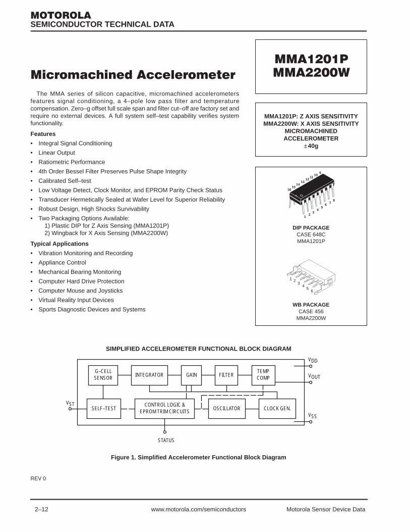
2–12 Motorola Sensor Device Datawww.motorola.com/semiconductors
The MMA series of silicon capacitive, micromachined accelerometersfeatures signal conditioning, a 4–pole low pass filter and temperaturecompensation. Zero–g offset full scale span and filter cut–off are factory set andrequire no external devices. A full system self–test capability verifies systemfunctionality.
Features
• Integral Signal Conditioning
• Linear Output
• Ratiometric Performance
• 4th Order Bessel Filter Preserves Pulse Shape Integrity
• Calibrated Self–test
• Low Voltage Detect, Clock Monitor, and EPROM Parity Check Status
• Transducer Hermetically Sealed at Wafer Level for Superior Reliability
• Robust Design, High Shocks Survivability
• Two Packaging Options Available:1) Plastic DIP for Z Axis Sensing (MMA1201P)2) Wingback for X Axis Sensing (MMA2200W)
Typical Applications
• Vibration Monitoring and Recording
• Appliance Control
• Mechanical Bearing Monitoring
• Computer Hard Drive Protection
• Computer Mouse and Joysticks
• Virtual Reality Input Devices
• Sports Diagnostic Devices and Systems
SIMPLIFIED ACCELEROMETER FUNCTIONAL BLOCK DIAGRAM
G–CELLSENSOR INTEGRATOR GAIN FILTER
TEMPCOMP
SELF–TESTCONTROL LOGIC &
EPROM TRIM CIRCUITS CLOCK GEN.OSCILLATOR
VDD
VOUT
VSS
VST
Figure 1. Simplified Accelerometer Functional Block Diagram
STATUS
REV 0
SEMICONDUCTOR TECHNICAL DATA
DIP PACKAGECASE 648CMMA1201P
MMA1201P: Z AXIS SENSITIVITYMMA2200W: X AXIS SENSITIVITY
MICROMACHINEDACCELEROMETER
±40g
WB PACKAGECASE 456
MMA2200W
1 23
45
6
12
34
56 7
8
910
1112
1314
1516

2–13Motorola Sensor Device Data www.motorola.com/semiconductors
MAXIMUM RATINGS (Maximum ratings are the limits to which the device can be exposed without causing permanent damage.)
Rating Symbol Value Unit
Powered Acceleration (all axes) Gpd 500 g
Unpowered Acceleration (all axes) Gupd 2000 g
Supply Voltage VDD –0.3 to +7.0 V
Drop Test(1) Ddrop 1.2 m
Storage Temperature Range Tstg –40 to +105 °C
NOTES:1. Dropped onto concrete surface from any axis.
ELECTRO STATIC DISCHARGE (ESD)
WARNING: This device is sensitive to electrostaticdischarge.
Although the Motorola accelerometers contain internal2kV ESD protection circuitry, extra precaution must be takenby the user to protect the chip from ESD. A charge of over
2000 volts can accumulate on the human body or associatedtest equipment. A charge of this magnitude can alter the per-formance or cause failure of the chip. When handling theaccelerometer, proper ESD precautions should be followedto avoid exposing the device to discharges which may bedetrimental to its performance.

2–14 Motorola Sensor Device Datawww.motorola.com/semiconductors
OPERATING CHARACTERISTICS(Unless otherwise noted: –40°C TA +85°C, 4.75 VDD 5.25, Acceleration = 0g, Loaded output(1))
Characteristic Symbol Min Typ Max Unit
Operating Range(2)
Supply Voltage(3)
Supply CurrentOperating Temperature RangeAcceleration Range
VDDIDDTA
gFS
4.754.040—
5.005.0—38
5.256.0+85—
VmA°Cg
Output SignalZero g (VDD = 5.0 V)(4)
Zero gSensitivity (TA = 25°C, VDD = 5.0 V)(5)
Sensitivity (VDD = 5.0 V)Bandwidth ResponseNonlinearity
VOFFVOFF,V
SSV
f–3dBNLOUT
2.20.44 VDD
47.59.33601.0
2.50.50 VDD
5010400—
2.80.56 VDD
52.510.7440+1.0
VV
mV/gmV/g/V
Hz% FSO
NoiseRMS (.01–1 kHz)Power Spectral DensityClock Noise (without RC load on output)(6)
nRMSnPSDnCLK
———
—1102.0
3.5——
mVrmsµV/(Hz1/2)
mVpk
Self–TestOutput ResponseInput LowInput HighInput Loading(7)
Response Time(8)
gSTVILVIHIINtST
20VSS
0.7 x VDD30—
———110
2.0
300.3 x VDD
VDD300
10
gVV
µAms
Status(12)(13)
Output Low (Iload = 100 µA)Output High (Iload = 100 µA)
VOLVOH
—VDD .8
——
0.4—
VV
Minimum Supply Voltage (LVD Trip) VLVD 2.7 3.25 4.0 V
Clock Monitor Fail Detection Frequency fmin 50 — 260 kHz
Output Stage PerformanceElectrical Saturation Recovery Time(9)
Full Scale Output Range (IOUT = 200 µA)Capacitive Load Drive(10)
Output Impedance
tDELAYVFSO
CLZO
—0.3——
0.2——
300
—VDD 0.3
100—
msVpFΩ
Mechanical CharacteristicsTransverse Sensitivity(11)
Package ResonanceVZX,YX
fPKG
——
—10
5.0—
% FSOkHz
NOTES:1. For a loaded output the measurements are observed after an RC filter consisting of a 1 kΩ resistor and a 0.01 µF capacitor to ground.2. These limits define the range of operation for which the part will meet specification.3. Within the supply range of 4.75 and 5.25 volts, the device operates as a fully calibrated linear accelerometer. Beyond these supply limits
the device may operate as a linear device but is not guaranteed to be in calibration.4. The device can measure both + and acceleration. With no input acceleration the output is at midsupply. For positive acceleration the output
will increase above VDD/2 and for negative acceleration the output will decrease below VDD/2.5. The device is calibrated at 20g.6. At clock frequency 70 kHz.7. The digital input pin has an internal pull–down current source to prevent inadvertent self test initiation due to external board level leakages.8. Time for the output to reach 90% of its final value after a self–test is initiated.9. Time for amplifiers to recover after an acceleration signal causing them to saturate.
10. Preserves phase margin (60°) to guarantee output amplifier stability.11. A measure of the device’s ability to reject an acceleration applied 90° from the true axis of sensitivity.12. The Status pin output is not valid following power–up until at least one rising edge has been applied to the self–test pin. The Status pin is
high whenever the self–test input is high.13. The Status pin output latches high if a Low Voltage Detection or Clock Frequency failure occurs, or the EPROM parity changes to odd. The
Status pin can be reset by a rising edge on self–test, unless a fault condition continues to exist.
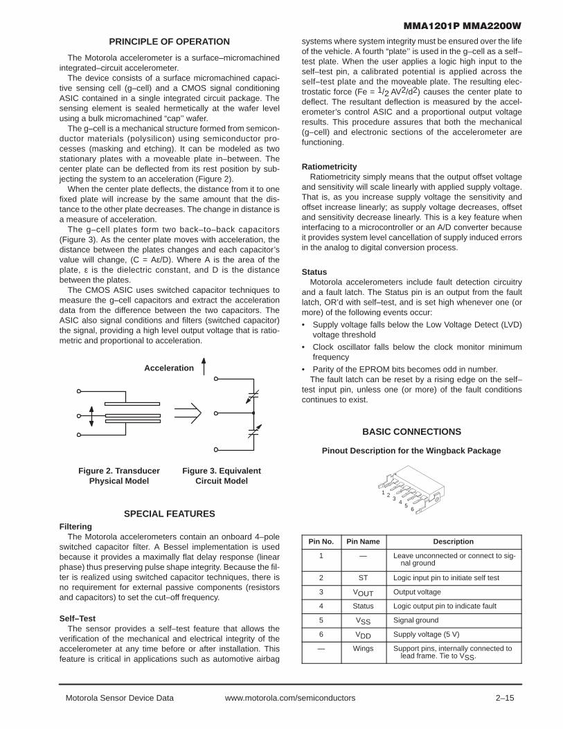
2–15Motorola Sensor Device Data www.motorola.com/semiconductors
PRINCIPLE OF OPERATION
The Motorola accelerometer is a surface–micromachinedintegrated–circuit accelerometer.
The device consists of a surface micromachined capaci-tive sensing cell (g–cell) and a CMOS signal conditioningASIC contained in a single integrated circuit package. Thesensing element is sealed hermetically at the wafer levelusing a bulk micromachined “cap’’ wafer.
The g–cell is a mechanical structure formed from semicon-ductor materials (polysilicon) using semiconductor pro-cesses (masking and etching). It can be modeled as twostationary plates with a moveable plate in–between. Thecenter plate can be deflected from its rest position by sub-jecting the system to an acceleration (Figure 2).
When the center plate deflects, the distance from it to onefixed plate will increase by the same amount that the dis-tance to the other plate decreases. The change in distance isa measure of acceleration.
The g–cell plates form two back–to–back capacitors(Figure 3). As the center plate moves with acceleration, thedistance between the plates changes and each capacitor’svalue will change, (C = Aε/D). Where A is the area of theplate, ε is the dielectric constant, and D is the distancebetween the plates.
The CMOS ASIC uses switched capacitor techniques tomeasure the g–cell capacitors and extract the accelerationdata from the difference between the two capacitors. TheASIC also signal conditions and filters (switched capacitor)the signal, providing a high level output voltage that is ratio-metric and proportional to acceleration.
Acceleration
Figure 2. TransducerPhysical Model
Figure 3. EquivalentCircuit Model
SPECIAL FEATURESFiltering
The Motorola accelerometers contain an onboard 4–poleswitched capacitor filter. A Bessel implementation is usedbecause it provides a maximally flat delay response (linearphase) thus preserving pulse shape integrity. Because the fil-ter is realized using switched capacitor techniques, there isno requirement for external passive components (resistorsand capacitors) to set the cut–off frequency.
Self–TestThe sensor provides a self–test feature that allows the
verification of the mechanical and electrical integrity of theaccelerometer at any time before or after installation. Thisfeature is critical in applications such as automotive airbag
systems where system integrity must be ensured over the lifeof the vehicle. A fourth “plate’’ is used in the g–cell as a self–test plate. When the user applies a logic high input to theself–test pin, a calibrated potential is applied across theself–test plate and the moveable plate. The resulting elec-trostatic force (Fe = 1/2 AV2/d2) causes the center plate todeflect. The resultant deflection is measured by the accel-erometer’s control ASIC and a proportional output voltageresults. This procedure assures that both the mechanical(g–cell) and electronic sections of the accelerometer arefunctioning.
RatiometricityRatiometricity simply means that the output offset voltage
and sensitivity will scale linearly with applied supply voltage.That is, as you increase supply voltage the sensitivity andoffset increase linearly; as supply voltage decreases, offsetand sensitivity decrease linearly. This is a key feature wheninterfacing to a microcontroller or an A/D converter becauseit provides system level cancellation of supply induced errorsin the analog to digital conversion process.
StatusMotorola accelerometers include fault detection circuitry
and a fault latch. The Status pin is an output from the faultlatch, OR’d with self–test, and is set high whenever one (ormore) of the following events occur:
• Supply voltage falls below the Low Voltage Detect (LVD)voltage threshold
• Clock oscillator falls below the clock monitor minimumfrequency
• Parity of the EPROM bits becomes odd in number.The fault latch can be reset by a rising edge on the self–
test input pin, unless one (or more) of the fault conditionscontinues to exist.
BASIC CONNECTIONS
Pinout Description for the Wingback Package
1 23
45
6
Pin No. Pin Name Description
1 — Leave unconnected or connect to sig-nal ground
2 ST Logic input pin to initiate self test
3 VOUT Output voltage
4 Status Logic output pin to indicate fault
5 VSS Signal ground
6 VDD Supply voltage (5 V)
— Wings Support pins, internally connected tolead frame. Tie to VSS.

2–16 Motorola Sensor Device Datawww.motorola.com/semiconductors
MMA2200WST
VDD
VSS
VOUT OUTPUTSIGNAL
R11 kΩ
3
C20.01 µF
2
6
5
LOGICINPUT
VDD
C10.1 µF
Figure 4. Wingback Accelerometer withRecommended Connection Diagram
STATUS4
Pinout Description for the DIP Package
16
15
14
13
12
11
10
9
1
2
3
4
5
6
7
8
N/C
N/C
N/C
ST
VOUT
STATUS
VSS
VDD
N/C
N/C
N/C
N/CN/C
N/C
N/C
N/C
N/C
Pin No. Pin Name Description
1 — Leave unconnected or connect tosignal ground.
2 thru 3 — No internal connection. Leave un-connected.
4 ST Logic input pin to initiate self test.
5 VOUT Output voltage
6 Status Logic output pin to indicate fault.
7 VSS Signal ground
8 VDD Supply voltage (5 V)
9 thru 13 Trim Pins Used for factory trim. Leave un-connected.
14 thru 16 — No internal connection. Leave un-connected.
MMA1201PST
VDD
VSS
VOUT OUTPUTSIGNAL
R11 kΩ
5
C20.01 µF
4
8
7
LOGICINPUT
VDD
C10.1 µF
Figure 5. DIP Accelerometer with RecommendedConnection Diagram
STATUS6
PCB Layout
P0
A/D IN
VRH
VSS
VDD
ST
VOUT
VSS
VDD
0.01 µFC1 kΩ
0.1 µF
C 0.1 µF
POWER SUPPLY
CR
C
0.1 µF
MICRO
CONTRO
LLERACCE
LERO
MET
ER
Figure 6. Recommend PCB Layout for InterfacingAccelerometer to Microcontroller
P1STATUS
NOTES:• Use a 0.1 µF capacitor on VDD to decouple the power
source.• Physical coupling distance of the accelerometer to the
microcontroller should be minimal.• Place a ground plane beneath the accelerometer to reduce
noise, the ground plane should be attached to all of theopen ended terminals shown in Figure 4.
• Use an RC filter of 1 kΩ and 0.01 µF on the output of theaccelerometer to minimize clock noise (from the switchedcapacitor filter circuit).
• PCB layout of power and ground should not couple powersupply noise.
• Accelerometer and microcontroller should not be a highcurrent path.
• A/D sampling rate and any external power supply switchingfrequency should be selected such that they do not inter-fere with the internal accelerometer sampling frequency.This will prevent aliasing errors.

2–17Motorola Sensor Device Data www.motorola.com/semiconductors
16 9
1 8
*
DIP PACKAGE
* When positioned as shown, the Earth’s gravity will result in a positive 1g output
Positive Acceleration Sensing Direction
WINGBACK PACKAGE
12
1 6
7
*
.090 .190 .290 .390 .490.000
.090
∅ .033
Measurement in inches
Drilling Patterns
WB PACKAGE DRILLING PATTERN
.0316X∅ .049
.0472X
.590 .680
ORDERING INFORMATION
Device Temperature Range Case No. Package
MMA1201P –40 to +85°C Case 648C–04 Plastic DIP
MMA2200W –40 to +85°C Case 456–06 Plastic Wingback

2–18 Motorola Sensor Device Datawww.motorola.com/semiconductors
The MMA series of silicon capacitive, micromachined accelerometersfeatures signal conditioning, a 4–pole low pass filter and temperaturecompensation. Zero–g offset full scale span and filter cut–off are factory set andrequire no external devices. A full system self–test capability verifies systemfunctionality.
Features
• Integral Signal Conditioning
• Linear Output
• Ratiometric Performance
• 4th Order Bessel Filter Preserves Pulse Shape Integrity
• Calibrated Self–test
• Low Voltage Detect, Clock Monitor, and EPROM Parity Check Status
• Transducer Hermetically Sealed at Wafer Level for Superior Reliability
• Robust Design, High Shock Survivability
Typical Applications
• Vibration Monitoring and Recording
• Appliance Control
• Mechanical Bearing Monitoring
• Computer Hard Drive Protection
• Computer Mouse and Joysticks
• Virtual Reality Input Devices
• Sports Diagnostic Devices and Systems
ORDERING INFORMATION
Device Temperature Range Case No. Package
MMA1220D –40 to +85°C Case 475–01 SOIC–16
SIMPLIFIED ACCELEROMETER FUNCTIONAL BLOCK DIAGRAM
G–CELLSENSOR INTEGRATOR GAIN FILTER
TEMPCOMP
SELF–TESTCONTROL LOGIC &
EPROM TRIM CIRCUITS CLOCK GEN.OSCILLATOR
VDD
VOUT
VSS
ST
Figure 1. Simplified Accelerometer Functional Block Diagram
STATUS
REV 0
SEMICONDUCTOR TECHNICAL DATA
MMA1220D: Z AXIS SENSITIVITYMICROMACHINEDACCELEROMETER
±8g
16 LEAD SOICCASE 475
16
91
8
10
11
12
13
14
15
16
8
7
6
5
4
3
2
1
9
N/C
N/C
N/C
STVOUT
STATUS
VSSVDD
N/C
N/C
N/C
N/CN/C
N/C
N/C
N/C
Pin Assignment

2–19Motorola Sensor Device Data www.motorola.com/semiconductors
MAXIMUM RATINGS (Maximum ratings are the limits to which the device can be exposed without causing permanent damage.)
Rating Symbol Value Unit
Powered Acceleration (all axes) Gpd 1500 g
Unpowered Acceleration (all axes) Gupd 2000 g
Supply Voltage VDD –0.3 to +7.0 V
Drop Test(1) Ddrop 1.2 m
Storage Temperature Range Tstg –40 to +105 °C
NOTES:1. Dropped onto concrete surface from any axis.
ELECTRO STATIC DISCHARGE (ESD)
WARNING: This device is sensitive to electrostaticdischarge.
Although the Motorola accelerometers contain internal2kV ESD protection circuitry, extra precaution must be takenby the user to protect the chip from ESD. A charge of over
2000 volts can accumulate on the human body or associatedtest equipment. A charge of this magnitude can alter the per-formance or cause failure of the chip. When handling theaccelerometer, proper ESD precautions should be followedto avoid exposing the device to discharges which may bedetrimental to its performance.

2–20 Motorola Sensor Device Datawww.motorola.com/semiconductors
OPERATING CHARACTERISTICS(Unless otherwise noted: –40°C TA +85°C, 4.75 VDD 5.25, Acceleration = 0g, Loaded output(1))
Characteristic Symbol Min Typ Max Unit
Operating Range(2)
Supply Voltage(3)
Supply CurrentOperating Temperature RangeAcceleration Range
VDDIDDTA
gFS
4.753.040—
5.005.0—8.0
5.256.0+85—
VmA°Cg
Output SignalZero g (VDD = 5.0 V)(4)
Zero gSensitivity (TA = 25°C, VDD = 5.0 V)(5)
SensitivityBandwidth ResponseNonlinearity
VOFFVOFF,V
SSV
f–3dBNLOUT
2.250.45 VDD
237.546.51501.0
2.50.50 VDD
25050250—
2.750.55 VDD
262.553.5350+3.0
VV
mV/gmV/g/V
Hz% FSO
NoiseRMS (10 Hz – 1 kHz)Clock Noise (without RC load on output)(6)
nRMSnCLK
——
—2.0
6.0—
mVrmsmVpk
Self–TestOutput ResponseInput LowInput HighInput Loading(7)
Response Time(8)
VSTVILVIHIINtST
0.2 VDDVSS
0.7 VDD50—
———100
2.0
0.3 VDD0.3 VDD
VDD200
10
VVV
µAms
Status(12)(13)
Output Low (Iload = 100 µA)Output High (Iload = 100 µA)
VOLVOH
—VDD 0.8
——
0.4—
VV
Minimum Supply Voltage (LVD Trip) VLVD 2.7 3.25 4.0 V
Clock Monitor Fail Detection Frequency fmin 50 — 260 kHz
Output Stage PerformanceElectrical Saturation Recovery Time(9)
Full Scale Output Range (IOUT = 200 µA)Capacitive Load Drive(10)
Output Impedance
tDELAYVFSO
CLZO
—VSS+0.25
——
2.0——
300
—VDD0.25
100—
msVpFΩ
Mechanical CharacteristicsTransverse Sensitivity(11)
Package ResonanceVXZ,YZ
fPKG
——
—10
5.0—
% FSOkHz
NOTES:1. For a loaded output the measurements are observed after an RC filter consisting of a 1 kΩ resistor and a 0.01 µF capacitor to ground.2. These limits define the range of operation for which the part will meet specification.3. Within the supply range of 4.75 and 5.25 volts, the device operates as a fully calibrated linear accelerometer. Beyond these supply limits
the device may operate as a linear device but is not guaranteed to be in calibration.4. The device can measure both + and acceleration. With no input acceleration the output is at midsupply. For positive acceleration the output
will increase above VDD/2 and for negative acceleration the output will decrease below VDD/2.5. The device is calibrated at 20g, 100 Hz. Sensitivity limits apply to 0 Hz acceleration.6. At clock frequency 70 kHz.7. The digital input pin has an internal pull–down current source to prevent inadvertent self test initiation due to external board level leakages.8. Time for the output to reach 90% of its final value after a self–test is initiated.9. Time for amplifiers to recover after an acceleration signal causing them to saturate.
10. Preserves phase margin (60°) to guarantee output amplifier stability.11. A measure of the device’s ability to reject an acceleration applied 90° from the true axis of sensitivity.12. The Status pin output is not valid following power–up until at least one rising edge has been applied to the self–test pin. The Status pin is
high whenever the self–test input is high.13. The Status pin output latches high if a Low Voltage Detection or Clock Frequency failure occurs, or the EPROM parity changes to odd. The
Status pin can be reset by a rising edge on self–test, unless a fault condition continues to exist.

2–21Motorola Sensor Device Data www.motorola.com/semiconductors
PRINCIPLE OF OPERATION
The Motorola accelerometer is a surface–micromachinedintegrated–circuit accelerometer.
The device consists of a surface micromachined capaci-tive sensing cell (g–cell) and a CMOS signal conditioningASIC contained in a single integrated circuit package. Thesensing element is sealed hermetically at the wafer levelusing a bulk micromachined “cap’’ wafer.
The g–cell is a mechanical structure formed from semicon-ductor materials (polysilicon) using semiconductor pro-cesses (masking and etching). It can be modeled as twostationary plates with a moveable plate in–between. Thecenter plate can be deflected from its rest position by sub-jecting the system to an acceleration (Figure 2).
When the center plate deflects, the distance from it to onefixed plate will increase by the same amount that the dis-tance to the other plate decreases. The change in distance isa measure of acceleration.
The g–cell plates form two back–to–back capacitors(Figure 3). As the center plate moves with acceleration, thedistance between the plates changes and each capacitor’svalue will change, (C = Aε/D). Where A is the area of theplate, ε is the dielectric constant, and D is the distancebetween the plates.
The CMOS ASIC uses switched capacitor techniques tomeasure the g–cell capacitors and extract the accelerationdata from the difference between the two capacitors. TheASIC also signal conditions and filters (switched capacitor)the signal, providing a high level output voltage that is ratio-metric and proportional to acceleration.
Acceleration
Figure 2. TransducerPhysical Model
Figure 3. EquivalentCircuit Model
SPECIAL FEATURESFiltering
The Motorola accelerometers contain an onboard 4–poleswitched capacitor filter. A Bessel implementation is usedbecause it provides a maximally flat delay response (linearphase) thus preserving pulse shape integrity. Because the fil-ter is realized using switched capacitor techniques, there isno requirement for external passive components (resistorsand capacitors) to set the cut–off frequency.
Self–TestThe sensor provides a self–test feature that allows the
verification of the mechanical and electrical integrity of theaccelerometer at any time before or after installation. Thisfeature is critical in applications such as automotive airbagsystems where system integrity must be ensured over the lifeof the vehicle. A fourth “plate’’ is used in the g–cell as a self–test plate. When the user applies a logic high input to theself–test pin, a calibrated potential is applied across theself–test plate and the moveable plate. The resulting elec-trostatic force (Fe = 1/2 AV2/d2) causes the center plate todeflect. The resultant deflection is measured by the accel-erometer’s control ASIC and a proportional output voltageresults. This procedure assures that both the mechanical(g–cell) and electronic sections of the accelerometer arefunctioning.
RatiometricityRatiometricity simply means that the output offset voltage
and sensitivity will scale linearly with applied supply voltage.That is, as you increase supply voltage the sensitivity andoffset increase linearly; as supply voltage decreases, offsetand sensitivity decrease linearly. This is a key feature wheninterfacing to a microcontroller or an A/D converter becauseit provides system level cancellation of supply induced errorsin the analog to digital conversion process.
StatusMotorola accelerometers include fault detection circuitry
and a fault latch. The Status pin is an output from the faultlatch, OR’d with self–test, and is set high whenever one (ormore) of the following events occur:• Supply voltage falls below the Low Voltage Detect (LVD)
voltage threshold• Clock oscillator falls below the clock monitor minimum
frequency• Parity of the EPROM bits becomes odd in number.
The fault latch can be reset by a rising edge on the self–test input pin, unless one (or more) of the fault conditionscontinues to exist.

2–22 Motorola Sensor Device Datawww.motorola.com/semiconductors
BASIC CONNECTIONS
10
11
12
13
14
15
16
8
7
6
5
4
3
2
1
9
N/C
N/C
N/C
STVOUT
STATUS
VSSVDD
N/C
N/C
N/C
N/CN/C
N/C
N/C
N/C
Pinout Description
Pin No. Pin Name Description
1 thru 3 VSS Redundant connections to the internalVSS and may be left unconnected.
4 ST Logic input pin used to initiate self–test.
5 VOUT Output voltage of the accelerometer.
6 STATUS Logic output pin used to indicate fault.
7 VSS The power supply ground.
8 VDD The power supply input.
9 thru 13 Trim pins Used for factory trim.Leave unconnected.
14 thru 16 — No internal connection.Leave unconnected.
MMA1220DST
VDD
VSS
VOUT OUTPUTSIGNAL
R11 kΩ
5
C20.01 µF
4
8
7
LOGICINPUT
VDD
C10.1 µF
Figure 4. SOIC Accelerometer with RecommendedConnection Diagram
STATUS6
PCB Layout
P0
A/D IN
VRH
VSS
VDD
ST
VOUT
VSS
VDD
0.01 µFC1 kΩ
0.1 µF
C 0.1 µF
POWER SUPPLY
CR
C
0.1 µF
MICRO
CONTRO
LLERACCE
LERO
MET
ER
Figure 5. Recommended PCB Layout for InterfacingAccelerometer to Microcontroller
P1STATUS
NOTES:
• Use a 0.1 µF capacitor on VDD to decouple the powersource.
• Physical coupling distance of the accelerometer to themicrocontroller should be minimal.
• Place a ground plane beneath the accelerometer to reducenoise, the ground plane should be attached to all of theopen ended terminals shown in Figure 4.
• Use an RC filter of 1 kΩ and 0.01 µF on the output of theaccelerometer to minimize clock noise (from the switchedcapacitor filter circuit).
• PCB layout of power and ground should not couple powersupply noise.
• Accelerometer and microcontroller should not be a highcurrent path.
• A/D sampling rate and any external power supply switchingfrequency should be selected such that they do not inter-fere with the internal accelerometer sampling frequency.This will prevent aliasing errors.

2–23Motorola Sensor Device Data www.motorola.com/semiconductors
* When positioned as shown, the Earth’s gravity will result in a positive 1g output
ACCELERATION SENSING DIRECTIONS
10
11
12
13
14
15
16
8
7
6
5
4
3
2
1
9
N/C
N/C
N/C
STVOUT
STATUSVSSVDD
N/C
N/C
N/C
N/CN/C
N/C
N/C
N/C
16–Pin SOIC PackageN/C pins are recommended to be left FLOATING–g
+g
Direction of Earth’s gravity field.*
DYNAMIC ACCELERATION
STATIC ACCELERATION
[ VOUT > 2.75 ]
[ VOUT < 2.75 ]
–1g
+1g
0g 0gVOUT = 2.50V VOUT = 2.50V
VOUT = 2.75V
VOUT = 2.25V

2–24 Motorola Sensor Device Datawww.motorola.com/semiconductors
The MMA series of silicon capacitive, micromachined accelerometersfeatures signal conditioning, a 2–pole low pass filter and temperaturecompensation. Zero–g offset full scale span and filter cut–off are factory set andrequire no external devices. A full system self–test capability verifies systemfunctionality.
Features
• Integral Signal Conditioning
• Linear Output
• 2nd Order Bessel Filter
• Calibrated Self–test
• EPROM Parity Check Status
• Transducer Hermetically Sealed at Wafer Level for Superior Reliability
• Robust Design, High Shock Survivability
Typical Applications
• Vibration Monitoring and Recording
• Appliance Control
• Mechanical Bearing Monitoring
• Computer Hard Drive Protection
• Computer Mouse and Joysticks
• Virtual Reality Input Devices
• Sports Diagnostic Devices and Systems
ORDERING INFORMATION
Device Temperature Range Case No. Package
MMA1250D –40 to +105°C Case 475–01 SOIC–16
SIMPLIFIED ACCELEROMETER FUNCTIONAL BLOCK DIAGRAM
G–CELLSENSOR INTEGRATOR GAIN FILTER
TEMP COMP& GAIN
SELF–TESTCONTROL LOGIC &
EPROM TRIM CIRCUITS CLOCK GEN.OSCILLATOR
VDD
VOUT
VSS
ST
Figure 1. Simplified Accelerometer Functional Block Diagram
STATUS
REV 1
SEMICONDUCTOR TECHNICAL DATA
MMA1250D: Z AXIS SENSITIVITYMICROMACHINEDACCELEROMETER
±5g
16 LEAD SOICCASE 475
16
91
8
10
11
12
13
14
15
16
8
7
6
5
4
3
2
1
9
VSSVSSVSS
VOUTSTATUS
VDDVSS
ST
N/C
N/C
N/C
N/CN/C
N/C
N/C
N/C
Pin Assignment

2–25Motorola Sensor Device Data www.motorola.com/semiconductors
MAXIMUM RATINGS (Maximum ratings are the limits to which the device can be exposed without causing permanent damage.)
Rating Symbol Value Unit
Powered Acceleration (all axes) gpd 1500 g
Unpowered Acceleration (all axes) gupd 2000 g
Supply Voltage VDD –0.3 to +7.0 V
Drop Test(1) Hdrop 1.2 m
Storage Temperature Range Tstg –40 to +125 °C
NOTES:1. Dropped onto concrete surface from any axis.
ELECTRO STATIC DISCHARGE (ESD)
WARNING: This device is sensitive to electrostaticdischarge.
Although the Motorola accelerometers contain internal2kV ESD protection circuitry, extra precaution must be takenby the user to protect the chip from ESD. A charge of over
2000 volts can accumulate on the human body or associatedtest equipment. A charge of this magnitude can alter the per-formance or cause failure of the chip. When handling the ac-celerometer, proper ESD precautions should be followed toavoid exposing the device to discharges which may be detri-mental to its performance.

2–26 Motorola Sensor Device Datawww.motorola.com/semiconductors
OPERATING CHARACTERISTICS(Unless otherwise noted: –40°C TA +105°C, 4.75 VDD 5.25, Acceleration = 0g, Loaded output(1))
Characteristic Symbol Min Typ Max Unit
Operating Range(2)
Supply Voltage(3)
Supply CurrentOperating Temperature RangeAcceleration Range
VDDIDDTA
gFS
4.751.140—
5.002.1—5
5.253.0
+105—
VmA°Cg
Output SignalZero g (TA = 25°C, VDD = 5.0 V)(4)
Zero g (VDD = 5.0 V)Sensitivity (TA = 25°C, VDD = 5.0 V)(5)
Sensitivity (VDD = 5.0 V)Bandwidth ResponseNonlinearity
VOFFVOFF
SS
f–3dBNLOUT
2.252.038037042.51.0
2.52.540040050—
2.753.0420
430.157.5+1.0
VV
mV/gmV/gHz
% FSO
NoiseRMS (0.1 Hz – 1.0 kHz)Spectral Density (RMS, 0.1 Hz – 1.0 kHz)(6)
nRMSnSD
——
2.0700
4.0—
mVrmsµg/√Hz
Self–TestOutput Response (VDD = 5.0 V)Input LowInput HighInput Loading(7)
Response Time(8)
VSTVILVIHIINtST
1.0VSS
0.7 VDD50—
1.25——125
10
1.50.3 VDD
VDD300
25
VVV
µAms
Status(12)(13)
Output Low (Iload = 100 µA)Output High (Iload = –100 µA)
VOLVOH
—VDD 0.8
——
0.4—
VV
Output Stage PerformanceElectrical Saturation Recovery Time(9)
Full Scale Output Range (IOUT = –200 µA)Capacitive Load Drive(10)
Output Impedance
tDELAYVFSO
CLZO
—VSS+0.25
——
———50
2.0VDD0.25
100—
msVpFΩ
Mechanical CharacteristicsTransverse Sensitivity(11) VXZ,YZ — — 5.0 % FSO
NOTES:1. For a loaded output the measurements are observed after an RC filter consisting of a 1 kΩ resistor and a 0.1 µF capacitor to ground.2. These limits define the range of operation for which the part will meet specification.3. Within the supply range of 4.75 and 5.25 volts, the device operates as a fully calibrated linear accelerometer. Beyond these supply limits
the device may operate as a linear device but is not guaranteed to be in calibration.4. The device can measure both + and acceleration. With no input acceleration the output is at midsupply. For positive acceleration the output
will increase above VDD/2 and for negative acceleration the output will decrease below VDD/2.5. Sensitivity limits apply to 0 Hz acceleration.6. At clock frequency 35 kHz.7. The digital input pin has an internal pull–down current source to prevent inadvertent self test initiation due to external board level leakages.8. Time for the output to reach 90% of its final value after a self–test is initiated.9. Time for amplifiers to recover after an acceleration signal causing them to saturate.
10. Preserves phase margin (60°) to guarantee output amplifier stability.11. A measure of the device’s ability to reject an acceleration applied 90° from the true axis of sensitivity.12. The Status pin output is not valid following power–up until at least one rising edge has been applied to the self–test pin. The Status pin is
high whenever the self–test input is high.13. The Status pin output latches high if the EPROM parity changes to odd. The Status pin can be reset by a rising edge on self–test, unless
a fault condition continues to exist.

2–27Motorola Sensor Device Data www.motorola.com/semiconductors
PRINCIPLE OF OPERATION
The Motorola accelerometer is a surface–micromachinedintegrated–circuit accelerometer.
The device consists of a surface micromachined capaci-tive sensing cell (g–cell) and a CMOS signal conditioningASIC contained in a single integrated circuit package. Thesensing element is sealed hermetically at the wafer level us-ing a bulk micromachined “cap’’ wafer.
The g–cell is a mechanical structure formed from semicon-ductor materials (polysilicon) using semiconductor pro-cesses (masking and etching). It can be modeled as twostationary plates with a moveable plate in–between. Thecenter plate can be deflected from its rest position by sub-jecting the system to an acceleration (Figure 2).
When the center plate deflects, the distance from it to onefixed plate will increase by the same amount that the dis-tance to the other plate decreases. The change in distance isa measure of acceleration.
The g–cell plates form two back–to–back capacitors (Fig-ure 3). As the center plate moves with acceleration, the dis-tance between the plates changes and each capacitor’svalue will change, (C = Aε/D). Where A is the area of theplate, ε is the dielectric constant, and D is the distance be-tween the plates.
The CMOS ASIC uses switched capacitor techniques tomeasure the g–cell capacitors and extract the accelerationdata from the difference between the two capacitors. TheASIC also signal conditions and filters (switched capacitor)the signal, providing a high level output voltage that is ratio-metric and proportional to acceleration.
Acceleration
Figure 2. TransducerPhysical Model
Figure 3. EquivalentCircuit Model
SPECIAL FEATURES
FilteringThe Motorola accelerometers contain an onboard 2–pole
switched capacitor filter. A Bessel implementation is usedbecause it provides a maximally flat delay response (linearphase) thus preserving pulse shape integrity. Because the fil-ter is realized using switched capacitor techniques, there isno requirement for external passive components (resistorsand capacitors) to set the cut–off frequency.
Self–TestThe sensor provides a self–test feature that allows the ver-
ification of the mechanical and electrical integrity of the ac-celerometer at any time before or after installation. Thisfeature is critical in applications such as automotive airbagsystems where system integrity must be ensured over the lifeof the vehicle. A fourth “plate’’ is used in the g–cell as a self–test plate. When the user applies a logic high input to theself–test pin, a calibrated potential is applied across theself–test plate and the moveable plate. The resulting elec-trostatic force (Fe = 1/2 AV2/d2) causes the center plate todeflect. The resultant deflection is measured by the accel-erometer’s control ASIC and a proportional output voltage re-sults. This procedure assures that both the mechanical(g–cell) and electronic sections of the accelerometer arefunctioning.
StatusMotorola accelerometers include fault detection circuitry
and a fault latch. The Status pin is an output from the faultlatch, OR’d with self–test, and is set high whenever the fol-lowing event occurs:
• Parity of the EPROM bits becomes odd in number.The fault latch can be reset by a rising edge on the self–
test input pin, unless one (or more) of the fault conditionscontinues to exist.

2–28 Motorola Sensor Device Datawww.motorola.com/semiconductors
BASIC CONNECTIONS
10
11
12
13
14
15
16
8
7
6
5
4
3
2
1
9
VSSVSSVSS
VOUTSTATUS
VDDVSS
ST
N/C
N/C
N/C
N/CN/C
N/C
N/C
N/C
Figure 4. Pinout Description
Pin No. Pin Name Description
1 thru 3 VSS Redundant connections to the internalVSS and may be left unconnected.
4 VOUT Output voltage of the accelerometer.
5 STATUS Logic output pin used to indicate fault.
6 VDD The power supply input.
7 VSS The power supply ground.
8 ST Logic input pin used to initiate self–test.
9 thru 13 Trim pins Used for factory trim.Leave unconnected.
14 thru 16 — No internal connection.Leave unconnected.
MMA1250DST
VDD
VSS
VOUT OUTPUTSIGNAL
R11 kΩ
4
C20.1 µF
8
6
7
LOGICINPUT
VDD
C10.1 µF
Figure 5. SOIC Accelerometer with RecommendedConnection Diagram
STATUS5
321
VSSVSSVSS
PCB Layout
P0
A/D IN
VRH
VSS
VDD
ST
VOUT
VSS
VDD
0.1 µFC1 kΩ
0.1 µF
C 0.1 µF
POWER SUPPLY
CR
C
0.1 µF
MICRO
CONTRO
LLERACCE
LERO
MET
ER
Figure 6. Recommended PCB Layout for InterfacingAccelerometer to Microcontroller
P1STATUS
NOTES:
• Use a 0.1 µF capacitor on VDD to decouple the powersource.
• Physical coupling distance of the accelerometer to the mi-crocontroller should be minimal.
• Place a ground plane beneath the accelerometer to reducenoise, the ground plane should be attached to all internalVSS terminals shown in Figure 4.
• Use an RC filter of 1 kΩ and 0.1 µF on the output of the ac-celerometer to minimize clock noise (from the switchedcapacitor filter circuit).
• PCB layout of power and ground should not couple powersupply noise.
• Accelerometer and microcontroller should not be a highcurrent path.
• A/D sampling rate and any external power supply switchingfrequency should be selected such that they do not inter-fere with the internal accelerometer sampling frequency.This will prevent aliasing errors.

2–29Motorola Sensor Device Data www.motorola.com/semiconductors
* When positioned as shown, the Earth’s gravity will result in a positive 1g output
ACCELERATION SENSING DIRECTIONS
10
11
12
13
14
15
16
8
7
6
5
4
3
2
1
9
VSSVSSVSS
VOUTSTATUS
VDDVSS
ST
N/C
N/C
N/C
N/CN/C
N/C
N/C
N/C
16–Pin SOIC PackageN/C pins are recommended to be left FLOATING–g
+g
Direction of Earth’s gravity field.*
DYNAMIC ACCELERATION
STATIC ACCELERATION
–1g
+1g
0g 0gVOUT = 2.50V VOUT = 2.50V
VOUT = 2.9V
VOUT = 2.1V

2–30 Motorola Sensor Device Datawww.motorola.com/semiconductors
The MMA series of silicon capacitive, micromachined accelerometersfeatures signal conditioning, a 2–pole low pass filter and temperaturecompensation. Zero–g offset full scale span and filter cut–off are factory set andrequire no external devices. A full system self–test capability verifies systemfunctionality.
Features
• Integral Signal Conditioning
• Linear Output
• 2nd Order Bessel Filter
• Calibrated Self–test
• EPROM Parity Check Status
• Transducer Hermetically Sealed at Wafer Level for Superior Reliability
• Robust Design, High Shock Survivability
Typical Applications
• Vibration Monitoring and Recording
• Appliance Control
• Mechanical Bearing Monitoring
• Computer Hard Drive Protection
• Computer Mouse and Joysticks
• Virtual Reality Input Devices
• Sports Diagnostic Devices and Systems
ORDERING INFORMATION
Device Temperature Range Case No. Package
MMA1260D –40 to +105°C Case 475–01 SOIC–16
SIMPLIFIED ACCELEROMETER FUNCTIONAL BLOCK DIAGRAM
G–CELLSENSOR INTEGRATOR GAIN FILTER
TEMP COMP& GAIN
SELF–TESTCONTROL LOGIC &
EPROM TRIM CIRCUITS CLOCK GEN.OSCILLATOR
VDD
VOUT
VSS
ST
Figure 1. Simplified Accelerometer Functional Block Diagram
STATUS
REV 1
SEMICONDUCTOR TECHNICAL DATA
MMA1260D: Z AXIS SENSITIVITYMICROMACHINEDACCELEROMETER
±1.5g
16 LEAD SOICCASE 475
16
91
8
10
11
12
13
14
15
16
8
7
6
5
4
3
2
1
9
VSSVSSVSS
VOUTSTATUS
VDDVSS
ST
N/C
N/C
N/C
N/CN/C
N/C
N/C
N/C
Pin Assignment

2–31Motorola Sensor Device Data www.motorola.com/semiconductors
MAXIMUM RATINGS (Maximum ratings are the limits to which the device can be exposed without causing permanent damage.)
Rating Symbol Value Unit
Powered Acceleration (all axes) gpd 1500 g
Unpowered Acceleration (all axes) gupd 2000 g
Supply Voltage VDD –0.3 to +7.0 V
Drop Test(1) Hdrop 1.2 m
Storage Temperature Range Tstg –40 to +125 °C
NOTES:1. Dropped onto concrete surface from any axis.
ELECTRO STATIC DISCHARGE (ESD)
WARNING: This device is sensitive to electrostaticdischarge.
Although the Motorola accelerometers contain internal2kV ESD protection circuitry, extra precaution must be takenby the user to protect the chip from ESD. A charge of over
2000 volts can accumulate on the human body or associatedtest equipment. A charge of this magnitude can alter the per-formance or cause failure of the chip. When handling the ac-celerometer, proper ESD precautions should be followed toavoid exposing the device to discharges which may be detri-mental to its performance.

2–32 Motorola Sensor Device Datawww.motorola.com/semiconductors
OPERATING CHARACTERISTICS(Unless otherwise noted: –40°C TA +105°C, 4.75 VDD 5.25, Acceleration = 0g, Loaded output(1))
Characteristic Symbol Min Typ Max Unit
Operating Range(2)
Supply Voltage(3)
Supply CurrentOperating Temperature RangeAcceleration Range
VDDIDDTA
gFS
4.751.140—
5.002.2—1.5
5.253.2
+105—
VmA°Cg
Output SignalZero g (TA = 25°C, VDD = 5.0 V)(4)
Zero g (VDD = 5.0 V)Sensitivity (TA = 25°C, VDD = 5.0 V)(5)
Sensitivity (VDD = 5.0 V)Bandwidth ResponseNonlinearity
VOFFVOFF
SS
f–3dBNLOUT
2.252.2
11401110401.0
2.52.5
1200120050—
2.752.8
1260129060
+1.0
VV
mV/gmV/gHz
% FSO
NoiseRMS (0.1 Hz – 1.0 kHz)Spectral Density (RMS, 0.1 Hz – 1.0 kHz)(6)
nRMSnSD
——
5.0500
9.0—
mVrmsµg/√Hz
Self–TestOutput Response (VDD = 5.0 V)Input LowInput HighInput Loading(7)
Response Time(8)
VSTVILVIHIINtST
0.3VSS
0.7 VDD50—
0.6——125
10
0.90.3 VDD
VDD300
25
VVV
µAms
Status(12)(13)
Output Low (Iload = 100 µA)Output High (Iload = –100 µA)
VOLVOH
—VDD 0.8
——
0.4—
VV
Output Stage PerformanceElectrical Saturation Recovery Time(9)
Full Scale Output Range (IOUT = –200 µA)Capacitive Load Drive(10)
Output Impedance
tDELAYVFSO
CLZO
—VSS+0.25
——
———50
2.0VDD0.25
100—
msVpFΩ
Mechanical CharacteristicsTransverse Sensitivity(11) VXZ,YZ — — 5.0 % FSO
NOTES:1. For a loaded output the measurements are observed after an RC filter consisting of a 1 kΩ resistor and a 0.1 µF capacitor to ground.2. These limits define the range of operation for which the part will meet specification.3. Within the supply range of 4.75 and 5.25 volts, the device operates as a fully calibrated linear accelerometer. Beyond these supply limits
the device may operate as a linear device but is not guaranteed to be in calibration.4. The device can measure both + and acceleration. With no input acceleration the output is at midsupply. For positive acceleration the output
will increase above VDD/2 and for negative acceleration the output will decrease below VDD/2.5. Sensitivity limits apply to 0 Hz acceleration.6. At clock frequency 35 kHz.7. The digital input pin has an internal pull–down current source to prevent inadvertent self test initiation due to external board level leakages.8. Time for the output to reach 90% of its final value after a self–test is initiated.9. Time for amplifiers to recover after an acceleration signal causing them to saturate.
10. Preserves phase margin (60°) to guarantee output amplifier stability.11. A measure of the device’s ability to reject an acceleration applied 90° from the true axis of sensitivity.12. The Status pin output is not valid following power–up until at least one rising edge has been applied to the self–test pin. The Status pin is
high whenever the self–test input is high.13. The Status pin output latches high if the EPROM parity changes to odd. The Status pin can be reset by a rising edge on self–test, unless
a fault condition continues to exist.

2–33Motorola Sensor Device Data www.motorola.com/semiconductors
PRINCIPLE OF OPERATION
The Motorola accelerometer is a surface–micromachinedintegrated–circuit accelerometer.
The device consists of a surface micromachined capaci-tive sensing cell (g–cell) and a CMOS signal conditioningASIC contained in a single integrated circuit package. Thesensing element is sealed hermetically at the wafer level us-ing a bulk micromachined “cap’’ wafer.
The g–cell is a mechanical structure formed from semicon-ductor materials (polysilicon) using semiconductor pro-cesses (masking and etching). It can be modeled as twostationary plates with a moveable plate in–between. Thecenter plate can be deflected from its rest position by sub-jecting the system to an acceleration (Figure 2).
When the center plate deflects, the distance from it to onefixed plate will increase by the same amount that the dis-tance to the other plate decreases. The change in distance isa measure of acceleration.
The g–cell plates form two back–to–back capacitors (Fig-ure 3). As the center plate moves with acceleration, the dis-tance between the plates changes and each capacitor’svalue will change, (C = Aε/D). Where A is the area of theplate, ε is the dielectric constant, and D is the distance be-tween the plates.
The CMOS ASIC uses switched capacitor techniques tomeasure the g–cell capacitors and extract the accelerationdata from the difference between the two capacitors. TheASIC also signal conditions and filters (switched capacitor)the signal, providing a high level output voltage that is ratio-metric and proportional to acceleration.
Acceleration
Figure 2. TransducerPhysical Model
Figure 3. EquivalentCircuit Model
SPECIAL FEATURES
FilteringThe Motorola accelerometers contain an onboard 2–pole
switched capacitor filter. A Bessel implementation is usedbecause it provides a maximally flat delay response (linearphase) thus preserving pulse shape integrity. Because the fil-ter is realized using switched capacitor techniques, there isno requirement for external passive components (resistorsand capacitors) to set the cut–off frequency.
Self–TestThe sensor provides a self–test feature that allows the ver-
ification of the mechanical and electrical integrity of the ac-celerometer at any time before or after installation. Thisfeature is critical in applications such as automotive airbagsystems where system integrity must be ensured over the lifeof the vehicle. A fourth “plate’’ is used in the g–cell as a self–test plate. When the user applies a logic high input to theself–test pin, a calibrated potential is applied across theself–test plate and the moveable plate. The resulting elec-trostatic force (Fe = 1/2 AV2/d2) causes the center plate todeflect. The resultant deflection is measured by the accel-erometer’s control ASIC and a proportional output voltage re-sults. This procedure assures that both the mechanical(g–cell) and electronic sections of the accelerometer arefunctioning.
StatusMotorola accelerometers include fault detection circuitry
and a fault latch. The Status pin is an output from the faultlatch, OR’d with self–test, and is set high whenever the fol-lowing event occurs:
• Parity of the EPROM bits becomes odd in number.The fault latch can be reset by a rising edge on the self–
test input pin, unless one (or more) of the fault conditionscontinues to exist.

2–34 Motorola Sensor Device Datawww.motorola.com/semiconductors
BASIC CONNECTIONS
10
11
12
13
14
15
16
8
7
6
5
4
3
2
1
9
VSSVSSVSS
VOUTSTATUS
VDDVSS
ST
N/C
N/C
N/C
N/CN/C
N/C
N/C
N/C
Figure 4. Pinout Description
Pin No. Pin Name Description
1 thru 3 VSS Redundant connections to the internalVSS and may be left unconnected.
4 VOUT Output voltage of the accelerometer.
5 STATUS Logic output pin used to indicate fault.
6 VDD The power supply input.
7 VSS The power supply ground.
8 ST Logic input pin used to initiate self–test.
9 thru 13 Trim pins Used for factory trim.Leave unconnected.
14 thru 16 — No internal connection.Leave unconnected.
Figure 5. SOIC Accelerometer with RecommendedConnection Diagram
MMA1260DST
VDD
VSS
VOUT OUTPUTSIGNAL
R11 kΩ
4
C20.1 µF
8
6
7
LOGICINPUT
VDD
C10.1 µF
STATUS5
321
VSSVSSVSS
PCB Layout
P0
A/D IN
VRH
VSS
VDD
ST
VOUT
VSS
VDD
0.1 µFC1 kΩ
0.1 µF
C 0.1 µF
POWER SUPPLY
CR
C
0.1 µF
MICRO
CONTRO
LLERACCE
LERO
MET
ER
Figure 6. Recommended PCB Layout for InterfacingAccelerometer to Microcontroller
P1STATUS
NOTES:
• Use a 0.1 µF capacitor on VDD to decouple the powersource.
• Physical coupling distance of the accelerometer to the mi-crocontroller should be minimal.
• Place a ground plane beneath the accelerometer to reducenoise, the ground plane should be attached to all internalVSS terminals shown in Figure 4.
• Use an RC filter of 1 kΩ and 0.1 µF on the output of the ac-celerometer to minimize clock noise (from the switchedcapacitor filter circuit).
• PCB layout of power and ground should not couple powersupply noise.
• Accelerometer and microcontroller should not be a highcurrent path.
• A/D sampling rate and any external power supply switchingfrequency should be selected such that they do not inter-fere with the internal accelerometer sampling frequency.This will prevent aliasing errors.

2–35Motorola Sensor Device Data www.motorola.com/semiconductors
* When positioned as shown, the Earth’s gravity will result in a positive 1g output
ACCELERATION SENSING DIRECTIONS
10
11
12
13
14
15
16
8
7
6
5
4
3
2
1
9
VSSVSSVSS
VOUTSTATUS
VDDVSS
ST
N/C
N/C
N/C
N/CN/C
N/C
N/C
N/C
16–Pin SOIC PackageN/C pins are recommended to be left FLOATING–g
+g
Direction of Earth’s gravity field.*
DYNAMIC ACCELERATION
STATIC ACCELERATION
–1g
+1g
0g 0gVOUT = 2.50V VOUT = 2.50V
VOUT = 3.7V
VOUT = 1.3V

2–36 Motorola Sensor Device Datawww.motorola.com/semiconductors
The MMA series of silicon capacitive, micromachined accelerometersfeatures signal conditioning, a 2–pole low pass filter and temperaturecompensation. Zero–g offset full scale span and filter cut–off are factory set andrequire no external devices. A full system self–test capability verifies systemfunctionality.
Features
• Integral Signal Conditioning
• Linear Output
• 2nd Order Bessel Filter
• Calibrated Self–test
• EPROM Parity Check Status
• Transducer Hermetically Sealed at Wafer Level for Superior Reliability
• Robust Design, High Shock Survivability
Typical Applications
• Vibration Monitoring and Recording
• Appliance Control
• Mechanical Bearing Monitoring
• Computer Hard Drive Protection
• Computer Mouse and Joysticks
• Virtual Reality Input Devices
• Sports Diagnostic Devices and Systems
ORDERING INFORMATION
Device Temperature Range Case No. Package
MMA1270D –40 to +105°C Case 475–01 SOIC–16
SIMPLIFIED ACCELEROMETER FUNCTIONAL BLOCK DIAGRAM
G–CELLSENSOR INTEGRATOR GAIN FILTER
TEMP COMP& GAIN
SELF–TESTCONTROL LOGIC &
EPROM TRIM CIRCUITS CLOCK GEN.OSCILLATOR
VDD
VOUT
VSS
ST
Figure 1. Simplified Accelerometer Functional Block Diagram
STATUS
REV 1
SEMICONDUCTOR TECHNICAL DATA
MMA1270D: Z AXIS SENSITIVITYMICROMACHINEDACCELEROMETER
±2.5g
16 LEAD SOICCASE 475
16
91
8
10
11
12
13
14
15
16
8
7
6
5
4
3
2
1
9
VSSVSSVSS
VOUTSTATUS
VDDVSS
ST
N/C
N/C
N/C
N/CN/C
N/C
N/C
N/C
Pin Assignment

2–37Motorola Sensor Device Data www.motorola.com/semiconductors
MAXIMUM RATINGS (Maximum ratings are the limits to which the device can be exposed without causing permanent damage.)
Rating Symbol Value Unit
Powered Acceleration (all axes) gpd 1500 g
Unpowered Acceleration (all axes) gupd 2000 g
Supply Voltage VDD –0.3 to +7.0 V
Drop Test(1) Hdrop 1.2 m
Storage Temperature Range Tstg –40 to +125 °C
NOTES:1. Dropped onto concrete surface from any axis.
ELECTRO STATIC DISCHARGE (ESD)
WARNING: This device is sensitive to electrostaticdischarge.
Although the Motorola accelerometers contain internal2kV ESD protection circuitry, extra precaution must be takenby the user to protect the chip from ESD. A charge of over
2000 volts can accumulate on the human body or associatedtest equipment. A charge of this magnitude can alter the per-formance or cause failure of the chip. When handling the ac-celerometer, proper ESD precautions should be followed toavoid exposing the device to discharges which may be detri-mental to its performance.
2–38 Motorola Sensor Device Datawww.motorola.com/semiconductors
OPERATING CHARACTERISTICS(Unless otherwise noted: –40°C TA +105°C, 4.75 VDD 5.25, Acceleration = 0g, Loaded output(1))
Characteristic Symbol Min Typ Max Unit
Operating Range(2)
Supply Voltage(3)
Supply CurrentOperating Temperature RangeAcceleration Range
VDDIDDTA
gFS
4.751.140—
5.002.1—2.5
5.253.0
+105—
VmA°Cg
Output SignalZero g (TA = 25°C, VDD = 5.0 V)(4)
Zero g (VDD = 5.0 V)Sensitivity (TA = 25°C, VDD = 5.0 V)(5)
Sensitivity(VDD = 5.0 V)Bandwidth ResponseNonlinearity
VOFFVOFF
SS
f–3dBNLOUT
2.252.2
712.5693.8
401.0
2.52.575075050—
2.752.8
787.5806.3
60+1.0
VV
mV/gmV/gHz
% FSO
NoiseRMS (0.1 Hz – 1.0 kHz)Spectral Density (RMS, 0.1 Hz – 1.0 kHz)(6)
nRMSnSD
——
3.5700
6.5—
mVrmsµg/√Hz
Self–TestOutput Response (VDD = 5.0 V)Input LowInput HighInput Loading(7)
Response Time(8)
VSTVILVIHIINtST
0.9VSS
0.7 VDD50—
1.25——125
10
1.60.3 VDD
VDD300
25
VVV
µAms
Status(12)(13)
Output Low (Iload = 100 µA)Output High (Iload = –100 µA)
VOLVOH
—VDD 0.8
——
0.4—
VV
Output Stage PerformanceElectrical Saturation Recovery Time(9)
Full Scale Output Range (IOUT = –200 µA)Capacitive Load Drive(10)
Output Impedance
tDELAYVFSO
CLZO
—VSS+0.25
——
———50
2.0VDD0.25
100—
msVpFΩ
Mechanical CharacteristicsTransverse Sensitivity(11) VXZ,YZ — — 5.0 % FSO
NOTES:1. For a loaded output the measurements are observed after an RC filter consisting of a 1 kΩ resistor and a 0.1 µF capacitor to ground.2. These limits define the range of operation for which the part will meet specification.3. Within the supply range of 4.75 and 5.25 volts, the device operates as a fully calibrated linear accelerometer. Beyond these supply limits
the device may operate as a linear device but is not guaranteed to be in calibration.4. The device can measure both + and acceleration. With no input acceleration the output is at midsupply. For positive acceleration the output
will increase above VDD/2 and for negative acceleration the output will decrease below VDD/2.5. Sensitivity limits apply to 0 Hz acceleration.6. At clock frequency 35 kHz.7. The digital input pin has an internal pull–down current source to prevent inadvertent self test initiation due to external board level leakages.8. Time for the output to reach 90% of its final value after a self–test is initiated.9. Time for amplifiers to recover after an acceleration signal causing them to saturate.
10. Preserves phase margin (60°) to guarantee output amplifier stability.11. A measure of the device’s ability to reject an acceleration applied 90° from the true axis of sensitivity.12. The Status pin output is not valid following power–up until at least one rising edge has been applied to the self–test pin. The Status pin is
high whenever the self–test input is high.13. The Status pin output latches high if the EPROM parity changes to odd. The Status pin can be reset by a rising edge on self–test, unless
a fault condition continues to exist.

2–39Motorola Sensor Device Data www.motorola.com/semiconductors
PRINCIPLE OF OPERATION
The Motorola accelerometer is a surface–micromachinedintegrated–circuit accelerometer.
The device consists of a surface micromachined capaci-tive sensing cell (g–cell) and a CMOS signal conditioningASIC contained in a single integrated circuit package. Thesensing element is sealed hermetically at the wafer level us-ing a bulk micromachined “cap’’ wafer.
The g–cell is a mechanical structure formed from semicon-ductor materials (polysilicon) using semiconductor pro-cesses (masking and etching). It can be modeled as twostationary plates with a moveable plate in–between. Thecenter plate can be deflected from its rest position by sub-jecting the system to an acceleration (Figure 2).
When the center plate deflects, the distance from it to onefixed plate will increase by the same amount that the dis-tance to the other plate decreases. The change in distance isa measure of acceleration.
The g–cell plates form two back–to–back capacitors (Fig-ure 3). As the center plate moves with acceleration, the dis-tance between the plates changes and each capacitor’svalue will change, (C = Aε/D). Where A is the area of theplate, ε is the dielectric constant, and D is the distance be-tween the plates.
The CMOS ASIC uses switched capacitor techniques tomeasure the g–cell capacitors and extract the accelerationdata from the difference between the two capacitors. TheASIC also signal conditions and filters (switched capacitor)the signal, providing a high level output voltage that is ratio-metric and proportional to acceleration.
Acceleration
Figure 2. TransducerPhysical Model
Figure 3. EquivalentCircuit Model
SPECIAL FEATURES
FilteringThe Motorola accelerometers contain an onboard 2–pole
switched capacitor filter. A Bessel implementation is usedbecause it provides a maximally flat delay response (linearphase) thus preserving pulse shape integrity. Because the fil-ter is realized using switched capacitor techniques, there isno requirement for external passive components (resistorsand capacitors) to set the cut–off frequency.
Self–TestThe sensor provides a self–test feature that allows the ver-
ification of the mechanical and electrical integrity of the ac-celerometer at any time before or after installation. Thisfeature is critical in applications such as automotive airbagsystems where system integrity must be ensured over the lifeof the vehicle. A fourth “plate’’ is used in the g–cell as a self–test plate. When the user applies a logic high input to theself–test pin, a calibrated potential is applied across theself–test plate and the moveable plate. The resulting elec-trostatic force (Fe = 1/2 AV2/d2) causes the center plate todeflect. The resultant deflection is measured by the accel-erometer’s control ASIC and a proportional output voltage re-sults. This procedure assures that both the mechanical(g–cell) and electronic sections of the accelerometer arefunctioning.
StatusMotorola accelerometers include fault detection circuitry
and a fault latch. The Status pin is an output from the faultlatch, OR’d with self–test, and is set high whenever the fol-lowing event occurs:
• Parity of the EPROM bits becomes odd in number.The fault latch can be reset by a rising edge on the self–
test input pin, unless one (or more) of the fault conditionscontinues to exist.

2–40 Motorola Sensor Device Datawww.motorola.com/semiconductors
BASIC CONNECTIONS
10
11
12
13
14
15
16
8
7
6
5
4
3
2
1
9
VSSVSSVSS
VOUTSTATUS
VDDVSS
ST
N/C
N/C
N/C
N/CN/C
N/C
N/C
N/C
Figure 4. Pinout Description
Pin No. Pin Name Description
1 thru 3 VSS Redundant connections to the internalVSS and may be left unconnected.
4 VOUT Output voltage of the accelerometer.
5 STATUS Logic output pin used to indicate fault.
6 VDD The power supply input.
7 VSS The power supply ground.
8 ST Logic input pin used to initiate self–test.
9 thru 13 Trim pins Used for factory trim.Leave unconnected.
14 thru 16 — No internal connection.Leave unconnected.
Figure 5. SOIC Accelerometer with RecommendedConnection Diagram
MMA1270DST
VDD
VSS
VOUT OUTPUTSIGNAL
R11 kΩ
4
C20.1 µF
8
6
7
LOGICINPUT
VDD
C10.1 µF
STATUS5
321
VSSVSSVSS
PCB Layout
P0
A/D IN
VRH
VSS
VDD
ST
VOUT
VSS
VDD
0.1 µFC1 kΩ
0.1 µF
C 0.1 µF
POWER SUPPLY
CR
C
0.1 µF
MICRO
CONTRO
LLERACCE
LERO
MET
ER
Figure 6. Recommended PCB Layout for InterfacingAccelerometer to Microcontroller
P1STATUS
NOTES:
• Use a 0.1 µF capacitor on VDD to decouple the powersource.
• Physical coupling distance of the accelerometer to the mi-crocontroller should be minimal.
• Place a ground plane beneath the accelerometer to reducenoise, the ground plane should be attached to all internalVSS terminals shown in Figure 4.
• Use an RC filter of 1 kΩ and 0.1 µF on the output of the ac-celerometer to minimize clock noise (from the switchedcapacitor filter circuit).
• PCB layout of power and ground should not couple powersupply noise.
• Accelerometer and microcontroller should not be a highcurrent path.
• A/D sampling rate and any external power supply switchingfrequency should be selected such that they do not inter-fere with the internal accelerometer sampling frequency.This will prevent aliasing errors.

2–41Motorola Sensor Device Data www.motorola.com/semiconductors
* When positioned as shown, the Earth’s gravity will result in a positive 1g output
ACCELERATION SENSING DIRECTIONS
10
11
12
13
14
15
16
8
7
6
5
4
3
2
1
9
VSSVSSVSS
VOUTSTATUS
VDDVSS
ST
N/C
N/C
N/C
N/CN/C
N/C
N/C
N/C
16–Pin SOIC PackageN/C pins are recommended to be left FLOATING–g
+g
Direction of Earth’s gravity field.*
DYNAMIC ACCELERATION
STATIC ACCELERATION
–1g
+1g
0g 0gVOUT = 2.50V VOUT = 2.50V
VOUT = 3.25V
VOUT = 1.75V

2–42 Motorola Sensor Device Datawww.motorola.com/semiconductors
The MMA series of silicon capacitive, micromachined accelerometersfeatures signal conditioning, a 4–pole low pass filter and temperaturecompensation. Zero–g offset full scale span and filter cut–off are factory set andrequire no external devices. A full system self–test capability verifies systemfunctionality.
Features
• Integral Signal Conditioning
• Linear Output
• Ratiometric Performance
• 4th Order Bessel Filter Preserves Pulse Shape Integrity
• Calibrated Self–test
• Low Voltage Detect, Clock Monitor, and EPROM Parity Check Status
• Transducer Hermetically Sealed at Wafer Level for Superior Reliability
• Robust Design, High Shocks Survivability
Typical Applications
• Vibration Monitoring and Recording
• Appliance Control
• Mechanical Bearing Monitoring
• Computer Hard Drive Protection
• Computer Mouse and Joysticks
• Virtual Reality Input Devices
• Sports Diagnostic Devices and Systems
SIMPLIFIED ACCELEROMETER FUNCTIONAL BLOCK DIAGRAM
G–CELLSENSOR INTEGRATOR GAIN FILTER
TEMPCOMP
SELF–TESTCONTROL LOGIC &
EPROM TRIM CIRCUITS CLOCK GEN.OSCILLATOR
VDD
VOUT
VSS
VST
Figure 1. Simplified Accelerometer Functional Block Diagram
STATUS
REV 0
SEMICONDUCTOR TECHNICAL DATA
MMA2201D: X AXIS SENSITIVITYMICROMACHINEDACCELEROMETER
±40g
16 LEAD SOICCASE 475
16
91
8

2–43Motorola Sensor Device Data www.motorola.com/semiconductors
MAXIMUM RATINGS (Maximum ratings are the limits to which the device can be exposed without causing permanent damage.)
Rating Symbol Value Unit
Powered Acceleration (all axes) Gpd 500 g
Unpowered Acceleration (all axes) Gupd 2000 g
Supply Voltage VDD –0.3 to +7.0 V
Drop Test(1) Ddrop 1.2 m
Storage Temperature Range Tstg –40 to +105 °C
NOTES:1. Dropped onto concrete surface from any axis.
ELECTRO STATIC DISCHARGE (ESD)
WARNING: This device is sensitive to electrostaticdischarge.
Although the Motorola accelerometers contain internal2kV ESD protection circuitry, extra precaution must be takenby the user to protect the chip from ESD. A charge of over
2000 volts can accumulate on the human body or associatedtest equipment. A charge of this magnitude can alter the per-formance or cause failure of the chip. When handling theaccelerometer, proper ESD precautions should be followedto avoid exposing the device to discharges which may bedetrimental to its performance.

2–44 Motorola Sensor Device Datawww.motorola.com/semiconductors
OPERATING CHARACTERISTICS(Unless otherwise noted: –40°C TA +85°C, 4.75 VDD 5.25, Acceleration = 0g, Loaded output(1))
Characteristic Symbol Min Typ Max Unit
Operating Range(2)
Supply Voltage(3)
Supply CurrentOperating Temperature RangeAcceleration Range
VDDIDDTA
gFS
4.754.040—
5.005.0—38
5.256.0+85—
VmA°Cg
Output SignalZero g (VDD = 5.0 V)(4)
Zero gSensitivity (TA = 25°C, VDD = 5.0 V)(5)
SensitivityBandwidth ResponseNonlinearity
VOFFVOFF,V
SSV
f–3dBNLOUT
2.30.44 VDD
47.59.33601.0
2.50.50 VDD
5010400—
2.70.56 VDD
52.510.7440+1.0
VV
mV/gmV/g/V
Hz% FSO
NoiseRMS (.01–1 kHz)Power Spectral DensityClock Noise (without RC load on output)(6)
nRMSnPSDnCLK
———
—1102.0
2.8——
mVrmsµV/(Hz1/2)
mVpk
Self–TestOutput ResponseInput LowInput HighInput Loading(7)
Response Time(8)
gSTVILVIHIINtST
10VSS
0.7 x VDD30—
12——110
2.0
140.3 x VDD
VDD300
10
gVV
µAms
Status(12)(13)
Output Low (Iload = 100 µA)Output High (Iload = 100 µA)
VOLVOH
—VDD .8
——
0.4—
VV
Minimum Supply Voltage (LVD Trip) VLVD 2.7 3.25 4.0 V
Clock Monitor Fail Detection Frequency fmin 150 — 400 kHz
Output Stage PerformanceElectrical Saturation Recovery Time(9)
Full Scale Output Range (IOUT = 200 µA)Capacitive Load Drive(10)
Output Impedance
tDELAYVFSO
CLZO
—0.3——
0.2——
300
—VDD 0.3
100—
msVpFΩ
Mechanical CharacteristicsTransverse Sensitivity(11)
Package ResonanceVZX,YX
fPKG
——
—10
5.0—
% FSOkHz
NOTES:1. For a loaded output the measurements are observed after an RC filter consisting of a 1 kΩ resistor and a 0.01 µF capacitor to ground.2. These limits define the range of operation for which the part will meet specification.3. Within the supply range of 4.75 and 5.25 volts, the device operates as a fully calibrated linear accelerometer. Beyond these supply limits
the device may operate as a linear device but is not guaranteed to be in calibration.4. The device can measure both + and acceleration. With no input acceleration the output is at midsupply. For positive acceleration the output
will increase above VDD/2 and for negative acceleration the output will decrease below VDD/2.5. The device is calibrated at 20g.6. At clock frequency 70 kHz.7. The digital input pin has an internal pull–down current source to prevent inadvertent self test initiation due to external board level leakages.8. Time for the output to reach 90% of its final value after a self–test is initiated.9. Time for amplifiers to recover after an acceleration signal causing them to saturate.
10. Preserves phase margin (60°) to guarantee output amplifier stability.11. A measure of the device’s ability to reject an acceleration applied 90° from the true axis of sensitivity.12. The Status pin output is not valid following power–up until at least one rising edge has been applied to the self–test pin. The Status pin is
high whenever the self–test input is high.13. The Status pin output latches high if a Low Voltage Detection or Clock Frequency failure occurs, or the EPROM parity changes to odd. The
Status pin can be reset by a rising edge on self–test, unless a fault condition continues to exist.

2–45Motorola Sensor Device Data www.motorola.com/semiconductors
PRINCIPLE OF OPERATION
The Motorola accelerometer is a surface–micromachinedintegrated–circuit accelerometer.
The device consists of a surface micromachined capaci-tive sensing cell (g–cell) and a CMOS signal conditioningASIC contained in a single integrated circuit package. Thesensing element is sealed hermetically at the wafer levelusing a bulk micromachined “cap’’ wafer.
The g–cell is a mechanical structure formed from semicon-ductor materials (polysilicon) using semiconductor pro-cesses (masking and etching). It can be modeled as twostationary plates with a moveable plate in–between. Thecenter plate can be deflected from its rest position by sub-jecting the system to an acceleration (Figure 2).
When the center plate deflects, the distance from it to onefixed plate will increase by the same amount that the dis-tance to the other plate decreases. The change in distance isa measure of acceleration.
The g–cell plates form two back–to–back capacitors(Figure 3). As the center plate moves with acceleration, thedistance between the plates changes and each capacitor’svalue will change, (C = Aε/D). Where A is the area of theplate, ε is the dielectric constant, and D is the distancebetween the plates.
The CMOS ASIC uses switched capacitor techniques tomeasure the g–cell capacitors and extract the accelerationdata from the difference between the two capacitors. TheASIC also signal conditions and filters (switched capacitor)the signal, providing a high level output voltage that is ratio-metric and proportional to acceleration.
Acceleration
Figure 2. TransducerPhysical Model
Figure 3. EquivalentCircuit Model
SPECIAL FEATURESFiltering
The Motorola accelerometers contain an onboard 4–poleswitched capacitor filter. A Bessel implementation is usedbecause it provides a maximally flat delay response (linearphase) thus preserving pulse shape integrity. Because the fil-ter is realized using switched capacitor techniques, there isno requirement for external passive components (resistorsand capacitors) to set the cut–off frequency.
Self–TestThe sensor provides a self–test feature that allows the
verification of the mechanical and electrical integrity of theaccelerometer at any time before or after installation. Thisfeature is critical in applications such as automotive airbagsystems where system integrity must be ensured over the lifeof the vehicle. A fourth “plate’’ is used in the g–cell as a self–test plate. When the user applies a logic high input to theself–test pin, a calibrated potential is applied across theself–test plate and the moveable plate. The resulting elec-trostatic force (Fe = 1/2 AV2/d2) causes the center plate todeflect. The resultant deflection is measured by the accel-erometer’s control ASIC and a proportional output voltageresults. This procedure assures that both the mechanical(g–cell) and electronic sections of the accelerometer arefunctioning.
RatiometricityRatiometricity simply means that the output offset voltage
and sensitivity will scale linearly with applied supply voltage.That is, as you increase supply voltage the sensitivity andoffset increase linearly; as supply voltage decreases, offsetand sensitivity decrease linearly. This is a key feature wheninterfacing to a microcontroller or an A/D converter becauseit provides system level cancellation of supply induced errorsin the analog to digital conversion process.
StatusMotorola accelerometers include fault detection circuitry
and a fault latch. The Status pin is an output from the faultlatch, OR’d with self–test, and is set high whenever one (ormore) of the following events occur:• Supply voltage falls below the Low Voltage Detect (LVD)
voltage threshold• Clock oscillator falls below the clock monitor minimum
frequency• Parity of the EPROM bits becomes odd in number.
The fault latch can be reset by a rising edge on the self–test input pin, unless one (or more) of the fault conditionscontinues to exist.
BASIC CONNECTIONS
10
11
12
13
14
15
16
8
7
6
5
4
3
2
1
9
N/C
N/C
N/C
STVOUT
N/C
VSSVDD
N/C
N/C
N/C
N/CN/C
N/C
N/C
N/C
Pinout Description

2–46 Motorola Sensor Device Datawww.motorola.com/semiconductors
Pin No. Pin Name Description
1 thru 3 — No internal connection. Leaveunconnected.
4 ST Logic input pin used to initiateself–test.
5 VOUT Output voltage of the accelerome-ter.
6 — No internal connection. Leaveunconnected.
7 VSS The power supply ground.
8 VDD The power supply input.
9 thru 13 Trim pins Used for factory trim. Leaveunconnected.
14 thru 16 — No internal connection. Leaveunconnected.
MMA2201DST
VDD
VSS
VOUT OUTPUTSIGNAL
R11 kΩ
5
C20.01 µF
4
8
7
LOGICINPUT
VDD
C10.1 µF
Figure 4. SOIC Accelerometer with RecommendedConnection Diagram
STATUS6
PCB Layout
P0
A/D IN
VRH
VSS
VDD
ST
VOUT
VSS
VDD
0.01 µFC1 kΩ
0.1 µF
C 0.1 µF
POWER SUPPLY
CR
C
0.1 µF
MICRO
CONTRO
LLERACCE
LERO
MET
ER
Figure 5. Recommend PCB Layout for InterfacingAccelerometer to Microcontroller
P1STATUS
NOTES:• Use a 0.1 µF capacitor on VDD to decouple the power
source.• Physical coupling distance of the accelerometer to the
microcontroller should be minimal.• Place a ground plane beneath the accelerometer to reduce
noise, the ground plane should be attached to all of theopen ended terminals shown in Figure 4.
• Use an RC filter of 1 kΩ and 0.01 µF on the output of theaccelerometer to minimize clock noise (from the switchedcapacitor filter circuit).
• PCB layout of power and ground should not couple powersupply noise.
• Accelerometer and microcontroller should not be a highcurrent path.
• A/D sampling rate and any external power supply switchingfrequency should be selected such that they do not inter-fere with the internal accelerometer sampling frequency.This will prevent aliasing errors.

2–47Motorola Sensor Device Data www.motorola.com/semiconductors
* When positioned as shown, the Earth’s gravity will result in a positive 1g output
Positive Acceleration Sensing Direction
10
11
12
13
14
15
16
8
7
6
5
4
3
2
1
9
N/C
N/C
N/C
SELF TESTXOUT
N/C
VSSVDD
N/C
N/C
N/C
N/CN/C
N/C
N/C
N/C
16–Pin SOIC PackageN/C pins are recommended to be left FLOATING
AXISORIENTATION
(ACCELERATIONFORCE
VECTOR)
–X +X
10 11 12 13 14 15 16
8 7 6 5 4 3 2 1
9
Direction of Earth’s gravity field.*
ORDERING INFORMATION
Device Temperature Range Case No. Package
MMA2201D 40 to +85°C Case 475–01 SOIC–16

2–48 Motorola Sensor Device Datawww.motorola.com/semiconductors
The MMA series of silicon capacitive, micromachined accelerometersfeatures signal conditioning, a 4–pole low pass filter and temperaturecompensation. Zero–g offset full scale span and filter cut–off are factory set andrequire no external devices. A full system self–test capability verifies systemfunctionality.
Features
• Integral Signal Conditioning
• Linear Output
• Ratiometric Performance
• 4th Order Bessel Filter Preserves Pulse Shape Integrity
• Calibrated Self–test
• Low Voltage Detect, Clock Monitor, and EPROM Parity Check Status
• Transducer Hermetically Sealed at Wafer Level for Superior Reliability
• Robust Design, High Shocks Survivability
Typical Applications
• Vibration Monitoring and Recording
• Impact Monitoring
• Appliance Control
• Mechanical Bearing Monitoring
• Computer Hard Drive Protection
• Computer Mouse and Joysticks
• Virtual Reality Input Devices
• Sports Diagnostic Devices and Systems
SIMPLIFIED ACCELEROMETER FUNCTIONAL BLOCK DIAGRAM
G–CELLSENSOR INTEGRATOR GAIN FILTER
TEMPCOMP
SELF–TESTCONTROL LOGIC &
EPROM TRIM CIRCUITS CLOCK GEN.OSCILLATOR
VDD
VOUT
VSS
ST
Figure 1. Simplified Accelerometer Functional Block Diagram
STATUS
REV 0
SEMICONDUCTOR TECHNICAL DATA
MMA2202D: X AXIS SENSITIVITYMICROMACHINEDACCELEROMETER
±50g
16 LEAD SOICCASE 475
16
91
8
10
11
12
13
14
15
16
8
7
6
5
4
3
2
1
9
N/C
N/C
N/C
STVOUT
STATUS
VSSVDD
N/C
N/C
N/C
N/CN/C
N/C
N/C
N/C
Pin Assignment

2–49Motorola Sensor Device Data www.motorola.com/semiconductors
MAXIMUM RATINGS (Maximum ratings are the limits to which the device can be exposed without causing permanent damage.)
Rating Symbol Value Unit
Powered Acceleration (all axes) Gpd 500 g
Unpowered Acceleration (all axes) Gupd 2000 g
Supply Voltage VDD –0.3 to +7.0 V
Drop Test(1) Ddrop 1.2 m
Storage Temperature Range Tstg –40 to +105 °C
NOTES:1. Dropped onto concrete surface from any axis.
ELECTRO STATIC DISCHARGE (ESD)
WARNING: This device is sensitive to electrostaticdischarge.
Although the Motorola accelerometers contain internal2kV ESD protection circuitry, extra precaution must be takenby the user to protect the chip from ESD. A charge of over
2000 volts can accumulate on the human body or associatedtest equipment. A charge of this magnitude can alter the per-formance or cause failure of the chip. When handling theaccelerometer, proper ESD precautions should be followedto avoid exposing the device to discharges which may bedetrimental to its performance.
2–50 Motorola Sensor Device Datawww.motorola.com/semiconductors
OPERATING CHARACTERISTICS(Unless otherwise noted: –40°C TA +85°C, 4.75 VDD 5.25, Acceleration = 0g, Loaded output(1))
Characteristic Symbol Min Typ Max Unit
Operating Range(2)
Supply Voltage(3)
Supply CurrentOperating Temperature RangeAcceleration Range
VDDIDDTA
gFS
4.754.040—
5.005.0—47
5.256.0+85—
VmA°Cg
Output SignalZero g (VDD = 5.0 V)(4)
Zero gSensitivity (TA = 25°C, VDD = 5.0 V)(5)
SensitivityBandwidth ResponseNonlinearity
VOFFVOFF,V
SSV
f–3dBNLOUT
2.30.44 VDD
377.43601.0
2.50.50 VDD
408
400—
2.70.56 VDD
438.6440+1.0
VV
mV/gmV/g/V
Hz% FSO
NoiseRMS (.01–1 kHz)Power Spectral DensityClock Noise (without RC load on output)(6)
nRMSnPSDnCLK
———
—1102.0
2.8——
mVrmsµV/(Hz1/2)
mVpk
Self–TestOutput ResponseInput LowInput HighInput Loading(7)
Response Time(8)
gSTVILVIHIINtST
10VSS
0.7 x VDD30—
12——110
2.0
140.3 x VDD
VDD300
10
gVV
µAms
Status(12)(13)
Output Low (Iload = 100 µA)Output High (Iload = 100 µA)
VOLVOH
—VDD .8
——
0.4—
VV
Minimum Supply Voltage (LVD Trip) VLVD 2.7 3.25 4.0 V
Clock Monitor Fail Detection Frequency fmin 150 — 400 kHz
Output Stage PerformanceElectrical Saturation Recovery Time(9)
Full Scale Output Range (IOUT = 200 µA)Capacitive Load Drive(10)
Output Impedance
tDELAYVFSO
CLZO
—0.3——
0.2——
300
—VDD 0.3
100—
msVpFΩ
Mechanical CharacteristicsTransverse Sensitivity(11)
Package ResonanceVZX,YX
fPKG
——
—10
5.0—
% FSOkHz
NOTES:1. For a loaded output the measurements are observed after an RC filter consisting of a 1 kΩ resistor and a 0.01 µF capacitor to ground.2. These limits define the range of operation for which the part will meet specification.3. Within the supply range of 4.75 and 5.25 volts, the device operates as a fully calibrated linear accelerometer. Beyond these supply limits
the device may operate as a linear device but is not guaranteed to be in calibration.4. The device can measure both + and acceleration. With no input acceleration the output is at midsupply. For positive acceleration the output
will increase above VDD/2 and for negative acceleration the output will decrease below VDD/2.5. The device is calibrated at 20g.6. At clock frequency 70 kHz.7. The digital input pin has an internal pull–down current source to prevent inadvertent self test initiation due to external board level leakages.8. Time for the output to reach 90% of its final value after a self–test is initiated.9. Time for amplifiers to recover after an acceleration signal causing them to saturate.
10. Preserves phase margin (60°) to guarantee output amplifier stability.11. A measure of the device’s ability to reject an acceleration applied 90° from the true axis of sensitivity.12. The Status pin output is not valid following power–up until at least one rising edge has been applied to the self–test pin. The Status pin is
high whenever the self–test input is high.13. The Status pin output latches high if a Low Voltage Detection or Clock Frequency failure occurs, or the EPROM parity changes to odd. The
Status pin can be reset by a rising edge on self–test, unless a fault condition continues to exist.

2–51Motorola Sensor Device Data www.motorola.com/semiconductors
PRINCIPLE OF OPERATION
The Motorola accelerometer is a surface–micromachinedintegrated–circuit accelerometer.
The device consists of a surface micromachined capaci-tive sensing cell (g–cell) and a CMOS signal conditioningASIC contained in a single integrated circuit package. Thesensing element is sealed hermetically at the wafer levelusing a bulk micromachined “cap’’ wafer.
The g–cell is a mechanical structure formed from semicon-ductor materials (polysilicon) using semiconductor pro-cesses (masking and etching). It can be modeled as twostationary plates with a moveable plate in–between. Thecenter plate can be deflected from its rest position by sub-jecting the system to an acceleration (Figure 2).
When the center plate deflects, the distance from it to onefixed plate will increase by the same amount that the dis-tance to the other plate decreases. The change in distance isa measure of acceleration.
The g–cell plates form two back–to–back capacitors(Figure 3). As the center plate moves with acceleration, thedistance between the plates changes and each capacitor’svalue will change, (C = Aε/D). Where A is the area of theplate, ε is the dielectric constant, and D is the distancebetween the plates.
The CMOS ASIC uses switched capacitor techniques tomeasure the g–cell capacitors and extract the accelerationdata from the difference between the two capacitors. TheASIC also signal conditions and filters (switched capacitor)the signal, providing a high level output voltage that is ratio-metric and proportional to acceleration.
Acceleration
Figure 2. TransducerPhysical Model
Figure 3. EquivalentCircuit Model
SPECIAL FEATURESFiltering
The Motorola accelerometers contain an onboard 4–poleswitched capacitor filter. A Bessel implementation is usedbecause it provides a maximally flat delay response (linearphase) thus preserving pulse shape integrity. Because the fil-ter is realized using switched capacitor techniques, there isno requirement for external passive components (resistorsand capacitors) to set the cut–off frequency.
Self–TestThe sensor provides a self–test feature that allows the
verification of the mechanical and electrical integrity of theaccelerometer at any time before or after installation. Thisfeature is critical in applications such as automotive airbagsystems where system integrity must be ensured over the lifeof the vehicle. A fourth “plate’’ is used in the g–cell as a self–test plate. When the user applies a logic high input to theself–test pin, a calibrated potential is applied across theself–test plate and the moveable plate. The resulting elec-trostatic force (Fe = 1/2 AV2/d2) causes the center plate todeflect. The resultant deflection is measured by the accel-erometer’s control ASIC and a proportional output voltageresults. This procedure assures that both the mechanical(g–cell) and electronic sections of the accelerometer arefunctioning.
RatiometricityRatiometricity simply means that the output offset voltage
and sensitivity will scale linearly with applied supply voltage.That is, as you increase supply voltage the sensitivity andoffset increase linearly; as supply voltage decreases, offsetand sensitivity decrease linearly. This is a key feature wheninterfacing to a microcontroller or an A/D converter becauseit provides system level cancellation of supply induced errorsin the analog to digital conversion process.
StatusMotorola accelerometers include fault detection circuitry
and a fault latch. The Status pin is an output from the faultlatch, OR’d with self–test, and is set high whenever one (ormore) of the following events occur:• Supply voltage falls below the Low Voltage Detect (LVD)
voltage threshold• Clock oscillator falls below the clock monitor minimum
frequency• Parity of the EPROM bits becomes odd in number.
The fault latch can be reset by a rising edge on the self–test input pin, unless one (or more) of the fault conditionscontinues to exist.
BASIC CONNECTIONS
10
11
12
13
14
15
16
8
7
6
5
4
3
2
1
9
N/C
N/C
N/C
STVOUT
STATUS
VDD
N/C
N/C
N/C
N/CN/C
N/C
N/C
N/C
Pinout Description
VSS

2–52 Motorola Sensor Device Datawww.motorola.com/semiconductors
Pin No. Pin Name Description
1 thru 3 — No internal connection. Leaveunconnected.
4 ST Logic input pin used to initiateself–test.
5 VOUT Output voltage of the accelerome-ter.
6 STATUS Logic output pin to indicate fault.
7 VSS The power supply ground.
8 VDD The power supply input.
9 thru 13 Trim pins Used for factory trim. Leaveunconnected.
14 thru 16 — No internal connection. Leaveunconnected.
MMA2202DST
VDD
VSS
VOUT OUTPUTSIGNAL
R11 kΩ
5
C20.01 µF
4
8
7
LOGICINPUT
VDD
C10.1 µF
Figure 4. SOIC Accelerometer with RecommendedConnection Diagram
STATUS6
PCB Layout
P0
A/D IN
VRH
VSS
VDD
ST
VOUT
VSS
VDD
0.01 µFC1 kΩ
0.1 µF
C 0.1 µF
POWER SUPPLY
CR
C
0.1 µF
MICRO
CONTRO
LLERACCE
LERO
MET
ER
Figure 5. Recommend PCB Layout for InterfacingAccelerometer to Microcontroller
P1STATUS
NOTES:• Use a 0.1 µF capacitor on VDD to decouple the power
source.• Physical coupling distance of the accelerometer to the
microcontroller should be minimal.• Place a ground plane beneath the accelerometer to reduce
noise, the ground plane should be attached to all of theopen ended terminals shown in Figure 4.
• Use an RC filter of 1 kΩ and 0.01 µF on the output of theaccelerometer to minimize clock noise (from the switchedcapacitor filter circuit).
• PCB layout of power and ground should not couple powersupply noise.
• Accelerometer and microcontroller should not be a highcurrent path.
• A/D sampling rate and any external power supply switchingfrequency should be selected such that they do not inter-fere with the internal accelerometer sampling frequency.This will prevent aliasing errors.
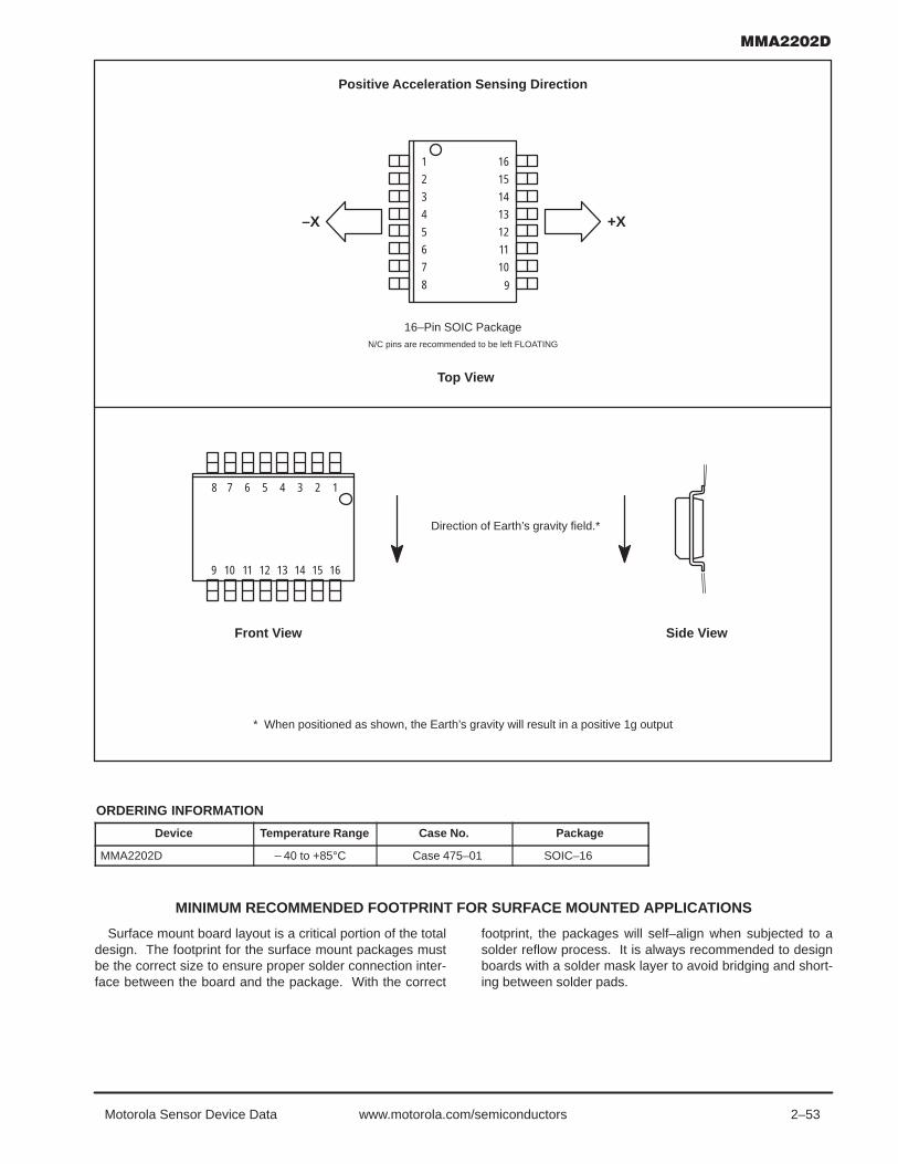
2–53Motorola Sensor Device Data www.motorola.com/semiconductors
* When positioned as shown, the Earth’s gravity will result in a positive 1g output
Positive Acceleration Sensing Direction
10
11
12
13
14
15
16
8
7
6
5
4
3
2
1
9
16–Pin SOIC PackageN/C pins are recommended to be left FLOATING
–X +X
10 11 12 13 14 15 16
8 7 6 5 4 3 2 1
9
Direction of Earth’s gravity field.*
Front View
Top View
Side View
ORDERING INFORMATION
Device Temperature Range Case No. Package
MMA2202D 40 to +85°C Case 475–01 SOIC–16
MINIMUM RECOMMENDED FOOTPRINT FOR SURFACE MOUNTED APPLICATIONS
Surface mount board layout is a critical portion of the totaldesign. The footprint for the surface mount packages mustbe the correct size to ensure proper solder connection inter-face between the board and the package. With the correct
footprint, the packages will self–align when subjected to asolder reflow process. It is always recommended to designboards with a solder mask layer to avoid bridging and short-ing between solder pads.

2–54 Motorola Sensor Device Datawww.motorola.com/semiconductors
Figure 6. Footprint SOIC–16 (Case 475–01)
0.380 in.9.65 mm
0.050 in.1.27 mm
0.024 in.0.610 mm
0.080 in.2.03 mm

2–55Motorola Sensor Device Data www.motorola.com/semiconductors
The MMA series of silicon capacitive, micromachined accelerometersfeatures signal conditioning, a 4–pole low pass filter and temperaturecompensation. Zero–g offset full scale span and filter cut–off are factory set andrequire no external devices. A full system self–test capability verifies systemfunctionality.
Features
• Integral Signal Conditioning
• Linear Output
• Ratiometric Performance
• 4th Order Bessel Filter Preserves Pulse Shape Integrity
• Calibrated Self–test
• Low Voltage Detect, Clock Monitor, and EPROM Parity Check Status
• Transducer Hermetically Sealed at Wafer Level for Superior Reliability
• Robust Design, High Shocks Survivability
Typical Applications
• Vibration Monitoring and Recording
• Impact Monitoring
• Appliance Control
• Mechanical Bearing Monitoring
• Computer Hard Drive Protection
• Computer Mouse and Joysticks
• Virtual Reality Input Devices
• Sports Diagnostic Devices and Systems
SIMPLIFIED ACCELEROMETER FUNCTIONAL BLOCK DIAGRAM
G–CELLSENSOR INTEGRATOR GAIN FILTER
TEMPCOMP
SELF–TESTCONTROL LOGIC &
EPROM TRIM CIRCUITS CLOCK GEN.OSCILLATOR
VDD
XOUT
VSS
ST
Figure 1. Simplified Accelerometer Functional Block Diagram
STATUS
YOUT
AVDD
REV 0
SEMICONDUCTOR TECHNICAL DATA
MMA3201D: X–Y AXIS SENSITIVITYMICROMACHINEDACCELEROMETER
±40g
20 LEAD SOICCASE 475A
20
111
10
14
15
16
17
18
19
20
8
7
6
5
4
3
2
1
13
N/C
N/C
N/C
STXOUT
STATUS
VDD
N/C
N/C
N/C
N/CN/C
N/C
N/C
N/C
Pin Assignment
12
10
9
11
VSS
AVDD
N/CYOUT
N/C

2–56 Motorola Sensor Device Datawww.motorola.com/semiconductors
MAXIMUM RATINGS (Maximum ratings are the limits to which the device can be exposed without causing permanent damage.)
Rating Symbol Value Unit
Powered Acceleration (all axes) Gpd 200 g
Unpowered Acceleration (all axes) Gupd 2000 g
Supply Voltage VDD –0.3 to +7.0 V
Drop Test(1) Ddrop 1.2 m
Storage Temperature Range Tstg –40 to +105 °C
NOTES:1. Dropped onto concrete surface from any axis.
ELECTRO STATIC DISCHARGE (ESD)
WARNING: This device is sensitive to electrostaticdischarge.
Although the Motorola accelerometers contain internal2kV ESD protection circuitry, extra precaution must be takenby the user to protect the chip from ESD. A charge of over
2000 volts can accumulate on the human body or associatedtest equipment. A charge of this magnitude can alter the per-formance or cause failure of the chip. When handling the ac-celerometer, proper ESD precautions should be followed toavoid exposing the device to discharges which may be detri-mental to its performance.

2–57Motorola Sensor Device Data www.motorola.com/semiconductors
OPERATING CHARACTERISTICS(Unless otherwise noted: –40°C TA +85°C, 4.75 VDD 5.25, X and Y Channels, Acceleration = 0g, Loaded output(1))
Characteristic Symbol Min Typ Max Unit
Operating Range(2)
Supply Voltage(3)
Supply CurrentOperating Temperature RangeAcceleration Range
VDDIDDTA
gFS
4.75640—
5.008—45
5.2510
+85—
VmA°Cg
Output SignalZero g (VDD = 5.0 V)(4)
Zero gSensitivity (TA = 25°C, VDD = 5.0 V)(5)
SensitivityBandwidth ResponseNonlinearity
VOFFVOFF,V
SSV
f–3dBNLOUT
2.20.44 VDD
459
3601.0
2.50.50 VDD
5010400—
2.80.56 VDD
5511
440+1.0
VV
mV/gmV/g/V
Hz% FSO
NoiseRMS (.01–1 kHz)Power Spectral DensityClock Noise (without RC load on output)(6)
nRMSnPSDnCLK
———
—1102.0
2.8——
mVrmsµV/(Hz1/2)
mVpk
Self–TestOutput ResponseInput LowInput HighInput Loading(7)
Response Time(8)
gSTVILVIHIINtST
9.6VSS
0.7 x VDD30—
12——110
2.0
14.40.3 x VDD
VDD300
—
gVV
µAms
Status(12)(13)
Output Low (Iload = 100 µA)Output High (Iload = 100 µA)
VOLVOH
—VDD .8
——
0.4—
VV
Minimum Supply Voltage (LVD Trip) VLVD 2.7 3.25 4.0 V
Clock Monitor Fail Detection Frequency fmin 50 — 260 kHz
Output Stage PerformanceElectrical Saturation Recovery Time(9)
Full Scale Output Range (IOUT = 200 µA)Capacitive Load Drive(10)
Output Impedance
tDELAYVFSO
CLZO
—0.3——
0.2——
300
—VDD 0.3
100—
msVpFΩ
Mechanical CharacteristicsTransverse Sensitivity(11)
Package ResonanceVZX,YX
fPKG
——
—10
5.0—
% FSOkHz
NOTES:1. For a loaded output the measurements are observed after an RC filter consisting of a 1 kΩ resistor and a 0.01 µF capacitor to ground.2. These limits define the range of operation for which the part will meet specification.3. Within the supply range of 4.75 and 5.25 volts, the device operates as a fully calibrated linear accelerometer. Beyond these supply limits
the device may operate as a linear device but is not guaranteed to be in calibration.4. The device can measure both + and acceleration. With no input acceleration the output is at midsupply. For positive acceleration the output
will increase above VDD/2 and for negative acceleration the output will decrease below VDD/2.5. The device is calibrated at 20g.6. At clock frequency 70 kHz.7. The digital input pin has an internal pull–down current source to prevent inadvertent self test initiation due to external board level leakages.8. Time for the output to reach 90% of its final value after a self–test is initiated.9. Time for amplifiers to recover after an acceleration signal causing them to saturate.
10. Preserves phase margin (60°) to guarantee output amplifier stability.11. A measure of the device’s ability to reject an acceleration applied 90° from the true axis of sensitivity.12. The Status pin output is not valid following power–up until at least one rising edge has been applied to the self–test pin. The Status pin is
high whenever the self–test input is high.13. The Status pin output latches high if a Low Voltage Detection or Clock Frequency failure occurs, or the EPROM parity changes to odd. The
Status pin can be reset by a rising edge on self–test, unless a fault condition continues to exist.

2–58 Motorola Sensor Device Datawww.motorola.com/semiconductors
PRINCIPLE OF OPERATION
The Motorola accelerometer is a surface–micromachinedintegrated–circuit accelerometer.
The device consists of a surface micromachined capaci-tive sensing cell (g–cell) and a CMOS signal conditioningASIC contained in a single integrated circuit package. Thesensing element is sealed hermetically at the wafer level us-ing a bulk micromachined “cap’’ wafer.
The g–cell is a mechanical structure formed from semicon-ductor materials (polysilicon) using semiconductor pro-cesses (masking and etching). It can be modeled as twostationary plates with a moveable plate in–between. Thecenter plate can be deflected from its rest position by sub-jecting the system to an acceleration (Figure 2).
When the center plate deflects, the distance from it to onefixed plate will increase by the same amount that the dis-tance to the other plate decreases. The change in distance isa measure of acceleration.
The g–cell plates form two back–to–back capacitors (Fig-ure 3). As the center plate moves with acceleration, the dis-tance between the plates changes and each capacitor’svalue will change, (C = Aε/D). Where A is the area of theplate, ε is the dielectric constant, and D is the distance be-tween the plates.
The CMOS ASIC uses switched capacitor techniques tomeasure the g–cell capacitors and extract the accelerationdata from the difference between the two capacitors. TheASIC also signal conditions and filters (switched capacitor)the signal, providing a high level output voltage that is ratio-metric and proportional to acceleration.
Acceleration
Figure 2. TransducerPhysical Model
Figure 3. EquivalentCircuit Model
SPECIAL FEATURESFiltering
The Motorola accelerometers contain an onboard 4–poleswitched capacitor filter. A Bessel implementation is usedbecause it provides a maximally flat delay response (linearphase) thus preserving pulse shape integrity. Because the fil-ter is realized using switched capacitor techniques, there isno requirement for external passive components (resistorsand capacitors) to set the cut–off frequency.
Self–TestThe sensor provides a self–test feature that allows the ver-
ification of the mechanical and electrical integrity of the ac-celerometer at any time before or after installation. Thisfeature is critical in applications such as automotive airbagsystems where system integrity must be ensured over the lifeof the vehicle. A fourth “plate’’ is used in the g–cell as a self–test plate. When the user applies a logic high input to theself–test pin, a calibrated potential is applied across theself–test plate and the moveable plate. The resulting elec-trostatic force (Fe = 1/2 AV2/d2) causes the center plate todeflect. The resultant deflection is measured by the accel-erometer’s control ASIC and a proportional output voltage re-sults. This procedure assures that both the mechanical(g–cell) and electronic sections of the accelerometer arefunctioning.
RatiometricityRatiometricity simply means that the output offset voltage
and sensitivity will scale linearly with applied supply voltage.That is, as you increase supply voltage the sensitivity andoffset increase linearly; as supply voltage decreases, offsetand sensitivity decrease linearly. This is a key feature wheninterfacing to a microcontroller or an A/D converter becauseit provides system level cancellation of supply induced errorsin the analog to digital conversion process.
StatusMotorola accelerometers include fault detection circuitry
and a fault latch. The Status pin is an output from the faultlatch, OR’d with self–test, and is set high whenever one (ormore) of the following events occur:• Supply voltage falls below the Low Voltage Detect (LVD)
voltage threshold• Clock oscillator falls below the clock monitor minimum
frequency• Parity of the EPROM bits becomes odd in number.
The fault latch can be reset by a rising edge on the self–test input pin, unless one (or more) of the fault conditionscontinues to exist.
BASIC CONNECTIONS
Pinout Description
14
15
16
17
18
19
20
8
7
6
5
4
3
2
1
13
N/C
N/C
N/C
STXOUT
STATUS
VDD
N/C
N/C
N/C
N/CN/C
N/C
N/C
N/C
12
10
9
11
VSS
AVDD
N/CYOUT
N/C

2–59Motorola Sensor Device Data www.motorola.com/semiconductors
Pin No. PinName
Description
1 thru 3 — Redundant Vss. Leave unconnected.
4 — No internal connection. Leave unconnected.
5 ST Logic input pin used to initiate self–test.
6 XOUT Output voltage of the accelerometer.X Direction.
7 STATUS Logic output pin to indicate fault.
8 VSS The power supply ground.
9 VDD Power supply input.
10 AVDD Power supply input (Analog).
11 YOUT Output voltage of the accelerometer.Y Direction.
12 thru 16 — Used for factory trim. Leave unconnected.
17 thru 20 — No internal connection. Leave unconnected.
10
XOUT
YOUT
MMA3201DST
VDD
VSS
X OUTPUTSIGNAL
R11 kΩ
C20.01 µF
5
9
8
LOGICINPUT
VDD
C10.1 µF
Figure 4. SOIC Accelerometer with RecommendedConnection Diagram
STATUS7
6
Y OUTPUTSIGNAL
C30.01 µF
R21 kΩ
AVDD
11
PCB Layout
P0
A/D IN
VRH
VSS
VDD
ST
YOUT
VSS
VDD
0.01 µFC1 kΩ
0.1 µF
C 0.1 µF
POWER SUPPLY
CR
C
0.1 µFM
ICROCO
NTROLLERAC
CELE
ROM
ETER
Figure 5. Recommend PCB Layout for InterfacingAccelerometer to Microcontroller
P1STATUS
A/D INXOUT R
0.01 µFC1 kΩ
NOTES:• Use a 0.1 µF capacitor on VDD to decouple the power
source.• Physical coupling distance of the accelerometer to the mi-
crocontroller should be minimal.• Place a ground plane beneath the accelerometer to reduce
noise, the ground plane should be attached to all of theopen ended terminals shown in Figure 4.
• Use an RC filter of 1 kΩ and 0.01 µF on the outputs of theaccelerometer to minimize clock noise (from the switchedcapacitor filter circuit).
• PCB layout of power and ground should not couple powersupply noise.
• Accelerometer and microcontroller should not be a highcurrent path.
• A/D sampling rate and any external power supply switchingfrequency should be selected such that they do not inter-fere with the internal accelerometer sampling frequency.This will prevent aliasing errors.

2–60 Motorola Sensor Device Datawww.motorola.com/semiconductors
* When positioned as shown, the Earth’s gravity will result in a positive 1g output
Positive Acceleration Sensing Direction
20–Pin SOIC PackageN/C pins are recommended to be left FLOATING
–X +X
Direction of Earth’s gravity field.*
Front View
Top View
Side View
14 15 16 17 18 19 20
8 7 6 5 4 3 2 1
1312
10 9
11
14
15
16
17
18
19
20
8
7
6
5
4
3
2
1
13
12
10
9
11
+Y
–Y
ORDERING INFORMATION
Device Temperature Range Case No. Package
MMA3201D 40 to +85°C Case 475A–01 SOIC–20
MINIMUM RECOMMENDED FOOTPRINT FOR SURFACE MOUNTED APPLICATIONS

2–61Motorola Sensor Device Data www.motorola.com/semiconductors
Surface mount board layout is a critical portion of the totaldesign. The footprint for the surface mount packages mustbe the correct size to ensure proper solder connection inter-face between the board and the package. With the correct
footprint, the packages will self–align when subjected to asolder reflow process. It is always recommended to designboards with a solder mask layer to avoid bridging and short-ing between solder pads.
Figure 6. Footprint SOIC–20 (Case 475A–01)
0.380 in.9.65 mm
0.050 in.1.27 mm
0.024 in.0.610 mm
0.080 in.2.03 mm

2–62 Motorola Sensor Device Datawww.motorola.com/semiconductors
By Wayne Chavez
INTRODUCTION
Today’s low cost accelerometers are highly integrateddevices employing features such as signal conditioning,filtering, offset compensation and self test. Combining thisfeature set with economical plastic packaging requires that thesignal conditioning circuitry be as small as possible. Oneapproach is to implement sampled data system and switchedcapacitor techniques as in the Motorola accelerometer.
As in all sampled data systems, precautions should betaken to avoid signal aliasing errors. This application notedescribes the Motorola accelerometer and how signal aliasingcan be introduced and more importantly minimized.
BACKGROUND
What is aliasing? Simply put, aliasing is the effect ofsampling a signal at an insufficient rate, thus creating another
signal at a frequency that is the difference between the originalsignal frequency and the sampling rate. A graphicalexplanation of aliasing is offered in Figure 1. In this figure, theupper trace shows a 50 kHz sinusoidal waveform. Note thatwhen sampled at a 45 kHz rate, denoted by the boxes, asinusoidal pattern is formed. Lowpass filtering the sampledpoints, to create a continuous signal, produces the 5 kHzwaveform shown in Figure 1 (lower). (The phase shift in thelower figure is due to the low–pass filter).
Aliased signals, like the one in Figure 1 (lower) are oftenunintentionally produced. Signal processing techniques arewell understood and sampling rates are chosen appropriately(i.e. Nyquist criteria). However, the assumption is that thesignals of interest are well characterized and have a limitedbandwidth. This assumption is not always true, as in the caseof wideband noise.
Figure 1. Aliased Signals
SEMICONDUCTOR APPLICATION NOTE
REV 1

2–63Motorola Sensor Device Data www.motorola.com/semiconductors
Given the brief example on how aliasing can occur, howdoes the accelerometer relate to aliasing? To answer thisquestion, a brief summary on how the accelerometer works isin order.
The accelerometer is a two chip acceleration sensingsolution. The first chip is the acceleration transducer, termedG–Cell, constructed by Micro Electro–Mechanical Systems(MEMS) technology. The G–Cell is a two capacitor elementwhere the capacitors are in series and share a common centerplate. The deflection in the center plate changes the capaci-tance of each capacitor which is measured by the second chip,termed control chip.
The control chip performs the signal conditioning (amplifica-tion, filtering, offset level shift) function in the system. This chipmeasures the G–Cell output using switched capacitor tech-niques. By the nature of switched cap techniques, the systemis a sampled data system operating at sampling frequency fs.The filter is switched capacitor, 4–pole Bessel implementationwith a –3 dB frequency of 400 Hz.
As a sampled data system, the accelerometer is not immuneto signal aliasing. However, given the accelerometer’s internalfilter, aliased signals will only appear in the output passbandwhen input signals are in the range | n• fs – fsignal | ≤ fBW. Wherefs is the sampling rate, fSignal is the input signal frequency, fBWis the filter bandwidth and n is a positive integer to account forall harmonics. The graphical representation is shown in Figure2. The bounds can be extended beyond fBW to ensure an aliasfree output.
Figure 2. Input signal frequency range where a signalwill be produced in the output passband.
KEEP OUT ZONE
Hzn*fs – fBW n*fs n*fs + fBW
ACCELEROMETER INPUT SIGNALS
The accelerometer is a ratiometric electro–mechanicaltransducer. Therefore, the input signals to the device are theacceleration and the input power source.
The acceleration input is limited in frequency bandwidth bythe geometry of the sensing, packaging, and mountingstructures that define the resonant frequency and response.This response is in the range of 10 kHz, however, the practicalrange is less than 600 Hz for most mechanical systems.Therefore, aliasing an acceleration signal is unlikely.
The power input signal is ideally dc. However, depending onthe application system architecture, the power supply line canbe riddled with high frequency components. For example, dcto dc converters can operate with switching frequenciesbetween 20 kHz and 200 kHz. This range encompasses thesampling rate of the accelerometer and point to the powersource as the culprit in producing aliased signal.
DEMONSTRATION OF ALIASING
Under zero acceleration conditions a 100 mVrms signal wasinjected onto the power supply line of 5.0 Vdc. The frequencyof the injected signal was tuned in to produce an alias in theaccelerometer’s passband. Figures 3 and 4 show thedifference in output when a high frequency signal is not and ispresent on the VCC pin of the accelerometer.
Figure 3. Normal Waveforms
(a)
(b)
(c)
1.0E+0
1.0E–1
1.0E–3
1.0E–2
1.0E–4
1.0E–5
1.0E–6
1.0E–741.0 41.2 41.4 41.6 41.8 42.0
FREQUENCY (kHz)
V rm
s
Vout
SAMPLINGFREQUENCY
1.0E+0
1.0E–1
1.0E–3
1.0E–2
1.0E–4
1.0E–5
1.0E–6
1.0E–741.0 41.2 41.4 41.6 41.8 42.0
FREQUENCY (kHz)
V rm
s
VCC
SAMPLINGFREQUENCY
1.0E+0
1.0E–1
1.0E–3
1.0E–2
1.0E–4
1.0E–5
1.0E–60 200 400 600 800 1000
FREQUENCY (Hz)
V rm
s
Vout
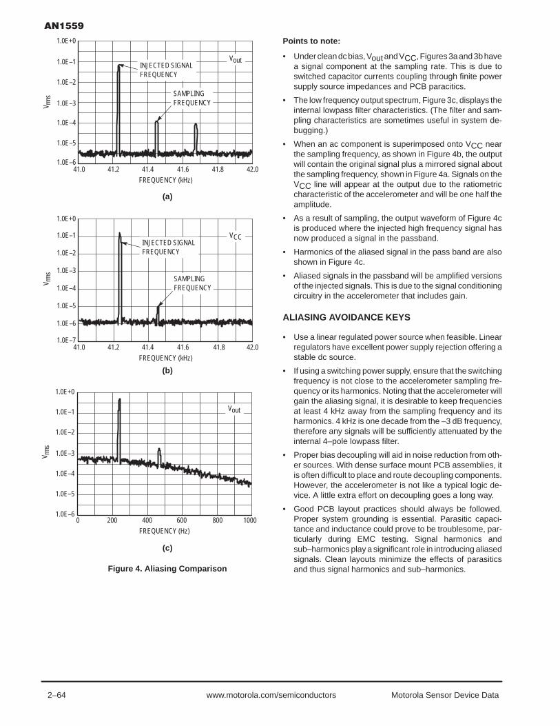
2–64 Motorola Sensor Device Datawww.motorola.com/semiconductors
Figure 4. Aliasing Comparison
(a)
(b)
(c)
SAMPLINGFREQUENCY
INJECTED SIGNALFREQUENCY
1.0E+0
1.0E–1
1.0E–3
1.0E–2
1.0E–4
1.0E–5
1.0E–641.0 41.2 41.4 41.6 41.8 42.0
FREQUENCY (kHz)
V rm
s
Vout
1.0E+0
1.0E–1
1.0E–3
1.0E–2
1.0E–4
1.0E–5
1.0E–6
1.0E–741.0 41.2 41.4 41.6 41.8 42.0
FREQUENCY (kHz)
V rm
s
VCC
SAMPLINGFREQUENCY
INJECTED SIGNALFREQUENCY
1.0E+0
1.0E–1
1.0E–3
1.0E–2
1.0E–4
1.0E–5
1.0E–60 200 400 600 800 1000
FREQUENCY (Hz)
V rm
s
Vout
Points to note:
• Under clean dc bias, Vout and VCC, Figures 3a and 3b havea signal component at the sampling rate. This is due toswitched capacitor currents coupling through finite powersupply source impedances and PCB paracitics.
• The low frequency output spectrum, Figure 3c, displays theinternal lowpass filter characteristics. (The filter and sam-pling characteristics are sometimes useful in system de-bugging.)
• When an ac component is superimposed onto VCC nearthe sampling frequency, as shown in Figure 4b, the outputwill contain the original signal plus a mirrored signal aboutthe sampling frequency, shown in Figure 4a. Signals on theVCC line will appear at the output due to the ratiometriccharacteristic of the accelerometer and will be one half theamplitude.
• As a result of sampling, the output waveform of Figure 4cis produced where the injected high frequency signal hasnow produced a signal in the passband.
• Harmonics of the aliased signal in the pass band are alsoshown in Figure 4c.
• Aliased signals in the passband will be amplified versionsof the injected signals. This is due to the signal conditioningcircuitry in the accelerometer that includes gain.
ALIASING AVOIDANCE KEYS
• Use a linear regulated power source when feasible. Linearregulators have excellent power supply rejection offering astable dc source.
• If using a switching power supply, ensure that the switchingfrequency is not close to the accelerometer sampling fre-quency or its harmonics. Noting that the accelerometer willgain the aliasing signal, it is desirable to keep frequenciesat least 4 kHz away from the sampling frequency and itsharmonics. 4 kHz is one decade from the –3 dB frequency,therefore any signals will be sufficiently attenuated by theinternal 4–pole lowpass filter.
• Proper bias decoupling will aid in noise reduction from oth-er sources. With dense surface mount PCB assemblies, itis often difficult to place and route decoupling components.However, the accelerometer is not like a typical logic de-vice. A little extra effort on decoupling goes a long way.
• Good PCB layout practices should always be followed.Proper system grounding is essential. Parasitic capaci-tance and inductance could prove to be troublesome, par-ticularly during EMC testing. Signal harmonics andsub–harmonics play a significant role in introducing aliasedsignals. Clean layouts minimize the effects of parasiticsand thus signal harmonics and sub–harmonics.

2–65Motorola Sensor Device Data www.motorola.com/semiconductors
Prepared by: C.S. ChuaSensor Application EngineeringSingapore, A/P
INTRODUCTIONThis application note describes the concept of measuring
impact of an object using an accelerometer, microcontrollerhardware/software and a liquid crystal display. Due to the widefrequency response of the accelerometer from d.c. to 400Hz,
the device is able to measure both the static acceleration fromthe Earth’s gravity and the shock or vibration from an impact.This design uses a 40G accelerometer (Motorola P/N:MMA2200W) yields a minimum acceleration range of –40G to+40G.
MMA2200W
FRONT VIEW
SIDE VIEW
PCB
1.0 g
+–
Figure 1. Orientation of Accelerometer
SEMICONDUCTOR APPLICATION NOTE
REV 2

2–66 Motorola Sensor Device Datawww.motorola.com/semiconductors
CONCEPT OF IMPACT MEASUREMENTDuring an impact, the accelerometer will be oriented as
shown in Figure 1 to measure the deceleration experienced by
the object from dc to 400Hz. Normally, the peak impact pulseis in the order of a few miniseconds. Figure 2 shows a typicalcrash waveform of a toy car having a stiff bumper.
PEAK IMPACT PULSE
10 20 30 40 50 600
TIME (ms)
DEC
ELER
ATIO
N (G
)
50
30
40
20
10
–10
0
–20
–30
–40
Figure 2. Typical Crash Pattern

2–67Motorola Sensor Device Data www.motorola.com/semiconductors
HARDWARE DESCRIPTION AND OPERATION
Since MMA2200W is fully signal–conditioned by its internalop–amp and temperature compensation, the output of theaccelerometer can be directly interfaced with an analog–to–digital (A/D) converter for digitization. A filter consists of oneRC network should be added if the connection between theoutput of the accelerometer and the A/D converter is a longtrack or cable. This stray capacitance may change the positionof the internal pole which would drive the output amplifier of theaccelerometer into oscillation or unstability. In this design, thecut–off frequency is chosen to be 15.9 kHz which also acts asan anti–alias filter for the A/D converter. The 3dB frequencycan be approximated by the following equation.
f–3dB1
2πRC
Referring to the schematic, Figure 3, the MMA2200Waccelerometer is connected to PORT D bit 5 and the output ofthe amplifier is connected to PORT D bit 6 of the micro-controller. This port is an input to the on–chip 8–bit analog–to–digital (A/D) converter. Typically, the accelerometer providesa signal output to the microprocessor of approximately 0.3 Vdcat –55g to 4.7 Vdc at +55g of acceleration. However, Motorolaonly guarantees the accuracy within ±40g range. Using thesame reference voltage for the A/D converter and accelerom-eter minimizes the number of additional components, but doessacrifice resolution. The resolution is defined by the following:
countVout
5 255
The count at 0g = [2.5/5] 255 ∝ 128The count at +25g = [3.5/5] 255 ∝ 179The count at –25g = [1.5/5] 255 ∝ 77
Therefore the resolution 0.5g/count
The output of the accelerometer is ratiometric to the voltageapplied to it. The accelerometer and the reference voltagesare connected to a common supply; this yields a system thatis ratiometric. By nature of this ratiometric system, variationsin the voltage of the power supplied to the system will have noeffect on the system accuracy.
The liquid crystal display (LCD) is directly driven from I/Oports A, B, and C on the microcontroller. The operation of a
LCD requires that the data and backplane (BP) pins must bedriven by an alternating signal. This function is provided by asoftware routine that toggles the data and backplane atapproximately a 30 Hz rate. Other than the LCD, one lightemitting diode (LED) are connected to the pulse lengthconverter (PLM) of the microcontroller. This LED will lights upfor 3 seconds when an impact greater or equal to 7g isdetected.
The microcontroller section of the system requires certainsupport hardware to allow it to function. The MC34064P–5provides an undervoltage sense function which is used toreset the microprocessor at system power–up. The 4 MHzcrystal provides the external portion of the oscillator functionfor clocking the microcontroller and provides a stable base fortime bases functions, for instance calculation of pulse rate.
SOFTWARE DESCRIPTION
Upon power–up the system, the LCD will display CAL forapproximately 4 seconds. During this period, the output of theaccelerometer are sampled and averaged to obtain the zerooffset voltage or zero acceleration. This value will be saved inthe RAM which is used by the equation below to calculate theimpact in term of g–force. One point to note is that theaccelerometer should remain stationary during the zerocalibration.
Impact [count countoffset ] resolution
In this software program, the output of the accelerometer iscalculated every 650µs. During an impact, the peak decelera-tion is measured and displayed on the LCD for 3 secondsbefore resetting it to zero. In the mean time, if a higher impactis detected, the value on the LCD will be updated accordingly.
However, when a low g is detected (e.g. 1.0g), the value willnot be displayed. Instead, more samples will be taken forfurther averaging to eliminate the random noise and highfrequency component. Due to the fact that tilting is a low g andlow frequency signal, large number of sampling is preferred toavoid unstable display. Moreover, the display value is not holdfor 3 seconds as in the case of an impact.
Figure 4 is a flowchart for the program that controls thesystem.

2–68 Motorola Sensor Device Datawww.motorola.com/semiconductors
MC34064
1
3
2
+5.0 V
+5.0 V R1
4.7 k
INPUT
/RESET
GND
JUMPER JUMPEROPEN
R5 R7R6
+5.0 V
+5.0 V
22 p
C4
22 p
C34.0 MHzR2 10 M
X1
270 R
R8
D1
100
C1
100 n
C2
+5.0 V
2
3
1
ON/OFF SWITCH
9.0 V BATTERY
10 n
C2′
0.1
C3′
0.1
C1′
+5.0 V 2
6
45
3GND
REWORK 1.0 k
BYPASSVS
OUTPUT SELF–TEST
GND
OUTPUT
INPUT
J1
J2
R3
R4
10 k
10 k
5.0 V REGULATOR
MC78L05ACP
3637 3435 67 285 40 1 8 3132 2930 11 10 9
16 23 22 21 20 19 18 17 12 27 26 25 24 15 14 13
G1
DP1
A1F1 C1
B1 D1
E1 G2
DP2
A2F2 C2
B2 D2
E2
G4 F4 A4 B4 C4
D4 E4 L
BP BP G3 F3 A3 B3 C3
D3 E3
DP3
49 48 47 46 45 44 43 42
PC1
PC0
PC3
PC2/
ECLK
PC5
PC4
PC6
PC7
20 21PL
MB
PLM
A
52 51SC
LKTD
O
2 1TC
MP2
TCM
P1
17 10VD
D
OSC
2
14 13 12 11 9 5 4 3
PD1/
AN1
PD0/
AN0
PD3/
AN3
PD2/
AN2
PD5/
AN5
PD4/
AN4
PD6/
AN6
PD7/
AN7
PA0
PA1
PA2
PA3
PA4
PA5
PA6
PA7
2930 2728 2526 2431
PB0
PB1
PB2
PB3
PB4
PB5
PB6
PB7
3738 3536 3334 3239
VRH
VRL
78
RO
I60
TCAP
223
TCAP
122
OSC
116
/RES
ET18
/IRQ
19
+5.0 V
MC68HC05B16CFN
LCD5657
MMA2200W
4
DP 3
DP 2
DP 1
LL
EF
GA
D
CB
Figure 3. Impact Measurement Schematic Drawing

2–69Motorola Sensor Device Data www.motorola.com/semiconductors
START
INITIALIZATION CLEAR I/O PORTS
DISPLAY “CAL” FOR4 SECONDS
AUTO–ZERO
READ ACCELEROMETER
CURRENTVALUE > 2.0 g?
IS THE IMPACT> 7.0 g?
ACTIVATE THEBUZZER / LED
IS THE CURRENTVALUE > PEAK VALUE?
IS THE PEAKVALUE BEEN DISPLAY >
3 SECOND?
PEAK VALUE = CURRENT VALUE
SET 3 SECOND FOR THE TIMER INTERRUPT
OUTPUT PEAK VALUETO LCD
ACCUMULATE THE DATA
IS THE NUMBEROF SAMPLES ACCUMULATED
= 128?
OUTPUT THE CURRENTVALUE TO LCD
TAKE THE AVERAGEOF THE DATA
IS THE 3 SECONDFOR THE PEAK VALUE
DISPLAY OVER?
Y
N
Y
N
Y
N
N
Y
Y
N
Y
N
Figure 4. Main Program Flowchart

2–70 Motorola Sensor Device Datawww.motorola.com/semiconductors
SOFTWARE SOURCE/ASSEMBLY PROGRAM CODE******************************************************************************* ** Accelerometer Demo Car Version 2.0 ** ** The following code is written for MC68HC705B16 using MMDS05 software ** Version 1.01 ** CASM05 – Command line assembler Version 3.04 ** P & E Microcomputer Systems, Inc. ** ** Written by : C.S. Chua ** 29 August 1996 ** ** ** Copyright Motorola Electronics Pte Ltd 1996 ** All rights Reserved ** ** This software is the property of Motorola Electronics Pte Ltd. ** ** Any usage or redistribution of this software without the express ** written consent of Motorola is strictly prohibited. ** ** Motorola reserves the right to make changes without notice to any ** products herein to improve reliability, function, or design. Motorola ** does not assume liability arising out of the application or use of any ** product or circuit described herein, neither does it convey license ** under its patents rights nor the rights of others. Motorola products are ** not designed, intended or authorised for use as component in systems ** intended to support or sustain life or for any other application in ** which the failure of the Motorola product could create a situation ** a situation where personal injury or death may occur. Should the buyer ** shall indemnify and hold Motorola products for any such unintended or ** unauthorised application, buyer shall indemnify and hold Motorola and ** its officers, employees, subsidiaries, affiliates, and distributors ** harmless against all claims, costs, damages, expenses and reasonable ** attorney fees arising out of, directly or indirectly, any claim of ** personal injury or death associated with such unintended or unauthorised ** use, even if such claim alleges that Motorola was negligent regarding ** the design or manufacture of the part. ** ** Motorola and the Motorola logo are registered trademarks of Motorola Inc.** ** Motorola Inc. is an equal opportunity/affirmative action employer. ** ************************************************************************************************************************************************************** ** Software Description ** ** This software is used to read the output of the accelerometer MMA2200W ** and display it to a LCD as gravity force. It ranges from –55g to +55g ** with 0g as zero acceleration or constant velocity. The resolution is ** 0.5g. ** ** The program will read from the accelerometer and hold the maximum ** deceleration value for about 3.0 seconds before resetting. At the same ** time, the buzzer/LED is activated if the impact is more than 7.0g. ** However, if the maximum deceleration changes before 3.0 seconds, it ** will update the display using the new value. Note that positive value ** implies deceleration whereas negative value implies acceleration ** ************************************************************************************************************************** ** Initialisation ** *******************************************PORTA EQU $00 ; Last digitPORTB EQU $01 ; Second digit (and negative sign)PORTC EQU $02 ; First digit (and decimal point)ADDATA EQU $08 ; ADC DataADSTAT EQU $09 ; ADC StatusPLMA EQU $0A ; Pulse Length Modulator (Output to Buzzer)MISC EQU $0C ; Miscellaneous Register (slow/fast mode)TCONTROL EQU $12 ; Timer control registerTSTATUS EQU $13 ; Timer Status RegisterOCMPHI1 EQU $16 ; Output Compare Register 1 High Byte

2–71Motorola Sensor Device Data www.motorola.com/semiconductors
OCMPLO1 EQU $17 ; Output Compare Register 1 Low ByteTCNTHI EQU $18 ; Timer Count Register High ByteTCNTLO EQU $19 ; Timer Count Register Low ByteOCMPHI2 EQU $1E ; Output Compare Register 2 High ByteOCMPLO2 EQU $1F ; Output Compare Register 2 Low Byte******************************************* ** User–defined RAM ** *******************************************SIGN EQU $54 ; Acceleration (–) or deceleration (+)PRESHI2 EQU $55 ; MSB of accumulated accelerationPRESHI EQU $56PRESLO EQU $57 ; LSB of accumulated accelerationPTEMPHI EQU $58 ; Acceleration High Byte (Temp storage)PTEMPLO EQU $59 ; Acceleration Low Byte (Temp storage)ACCHI EQU $5A ; Temp storage of acc value (High byte)ACCLO EQU $5B ; (Low byte)ADCOUNTER EQU $5C ; Sampling CounterAVERAGE_H EQU $5D ; MSB of the accumulated data of low gAVERAGE_M EQU $5EAVERAGE_L EQU $5F ; LSB of the accumulated data of low gSHIFT_CNT EQU $60 ; Counter for shifting the accumulated dataAVE_CNT1 EQU $61 ; Number of samples in the accumulated dataAVE_CNT2 EQU $75TEMPTCNTHI EQU $62 ; Temp storage for Timer count registerTEMPTCNTLO EQU $63 ; Temp storage for Timer count registerDECHI EQU $64 ; Decimal digit high byteDECLO EQU $65 ; Decimal digit low byteDCOFFSETHI EQU $66 ; DC offset of the output (high byte)DCOFFSETLO EQU $67 ; DC offset of the output (low byte)MAXACC EQU $68 ; Maximum accelerationTEMPHI EQU $69TEMPLO EQU $6ATEMP1 EQU $6B ; Temporary location for ACC during delayTEMP2 EQU $6C ; Temporary location for ACC during ISRDIV_LO EQU $6D ; No of sampling (low byte)DIV_HI EQU $6E ; No of sampling (high byte)NO_SHIFT EQU $6F ; No of right shift to get average valueZERO_ACC EQU $70 ; Zero acceleration in no of ADC stepsHOLD_CNT EQU $71 ; Hold time counterHOLD_DONE EQU $72 ; Hold time up flagSTART_TIME EQU $73 ; Start of count down flagRSHIFT EQU $74 ; No of shifting required for division ORG $300 ; ROM space 0300 to 3DFE (15,104 bytes) DB $FC ; Display ”0” DB $30 ; Display ”1” DB $DA ; Display ”2” DB $7A ; Display ”3” DB $36 ; Display ”4” DB $6E ; Display ”5” DB $EE ; Display ”6” DB $38 ; Display ”7” DB $FE ; Display ”8” DB $7E ; Display ”9”HUNDREDHI DB $00 ; High byte of hundredsHUNDREDLO DB $64 ; Low byte of hundredsTENHI DB $00 ; High byte of tensTENLO DB $0A ; Low byte of tens******************************************* ** Program starts here upon hard reset ** *******************************************RESET CLR PORTC ; Port C = 0 CLR PORTB ; Port B = 0 CLR PORTA ; Port A = 0 LDA #$FF STA $06 ; Port C as output STA $05 ; Port B as output STA $04 ; Port A as output LDA TSTATUS ; Dummy read the timer status register CLR OCMPHI2 ; so as to clear the OCF CLR OCMPHI1 LDA OCMPLO2 JSR COMPRGT CLR START_TIME

2–72 Motorola Sensor Device Datawww.motorola.com/semiconductors
LDA #$40 ; Enable the output compare interrupt STA TCONTROL CLI ; Interrupt begins here LDA #$CC ; Port C = 1100 1100 Letter ”C” STA PORTC LDA #$BE ; Port B = 1011 1110 Letter ”A” STA PORTB LDA #$C4 ; Port A = 1100 0100 Letter ”L” STA PORTA LDA #16IDLE JSR DLY20 ; Idling for a while (16*0.125 = 2 sec) DECA ; for the zero offset to stabilize BNE IDLE ; before perform auto–zero LDA #$00 ; Sample the data 32,768 times and take STA DIV_LO ; the average 8000 H = 32,768 LDA #$80 ; Right shift of 15 equivalent to divide STA DIV_HI ; by 32,768 LDA #!15 ; Overall sampling time = 1.033 s) STA NO_SHIFT JSR READAD ; Zero acceleration calibration LDX #5 ; Calculate the zero offset LDA PTEMPLO ; DC offset = PTEMPLO * 5 STA ZERO_ACC MUL STA DCOFFSETLO ; Save the zero offset in the RAM TXA STA DCOFFSETHI CLR HOLD_CNT LDA #$10 ; Sample the data 16 times and take STA DIV_LO ; the average 0100 H = 16 LDA #$00 ; Right shift of 4 equivalent to divide STA DIV_HI ; by 16 LDA #$4 ; Overall sampling time = 650 us STA NO_SHIFT LDA ZERO_ACC ; Display 0.0g at the start STA MAXACC JSR ADTOLCD CLR START_TIME CLR AVE_CNT1 CLR AVE_CNT2 CLR SHIFT_CNT CLR AVERAGE_L CLR AVERAGE_M CLR AVERAGE_HREPEAT JSR READAD ; Read acceleration from ADC LDA ZERO_ACC ADD #$04 CMP PTEMPLO BLO CRASH ; If the acceleration < 2.0g LDA PTEMPLO ; Accumulate the averaged results ADD AVERAGE_L ; for 128 times and take the averaging STA AVERAGE_L ; again to achieve more stable CLRA ; reading at low g ADC AVERAGE_M STA AVERAGE_M CLRA ADC AVERAGE_H STA AVERAGE_H LDA #$01 ADD AVE_CNT1 STA AVE_CNT1 CLRA ADC AVE_CNT2 STA AVE_CNT2 CMP #$04 BNE REPEAT LDA AVE_CNT1 CMP #$00 BNE REPEATSHIFTING INC SHIFT_CNT ; Take the average of the 128 samples LSR AVERAGE_H ROR AVERAGE_M ROR AVERAGE_L LDA SHIFT_CNT CMP #$0A BLO SHIFTING LDA AVERAGE_L

2–73Motorola Sensor Device Data www.motorola.com/semiconductors
STA PTEMPLO LDA HOLD_CNT ; Check if the hold time of crash data CMP #$00 ; is up BNE NON–CRASH LDA PTEMPLO ; If yes, display the current acceleration STA MAXACC ; value JSR ADTOLCD BRA NON–CRASHCRASH LDA ZERO_ACC ADD #$0E ; If the crash is more than 7g CMP PTEMPLO ; 7g = 0E H * 0.5 BHS NO_INFLATE LDA #$FF ; activate the LED STA PLMANO_INFLATE JSR MAXVALUE ; Display the peak acceleration JSR ADTOLCDNON–CRASH CLR SHIFT_CNT CLR AVE_CNT1 CLR AVE_CNT2 CLR AVERAGE_L CLR AVERAGE_M CLR AVERAGE_H BRA REPEAT ; Repeat the whole process******************************************* ** Delay Subroutine ** (162 * 0.7725 ms = 0.125 sec) ** *******************************************DLY20 STA TEMP1 LDA #!162 ; 1 unit = 0.7725 msOUTLP CLRXINNRLP DECX BNE INNRLP DECA BNE OUTLP LDA TEMP1 RTS******************************************* ** Reading the ADC data X times ** and take the average ** X is defined by DIV_HI and DIV_LO ** *******************************************READAD LDA #$25 STA ADSTAT ; AD status = 25H CLR PRESHI2 CLR PRESHI ; Clear the memory CLR PRESLO CLRX CLR ADCOUNTERLOOP128 TXA CMP #$FF BEQ INC_COUNT BRA CONTINC_COUNT INC ADCOUNTERCONT LDA ADCOUNTER ; If ADCOUNTER = X CMP DIV_HI ; Clear bit = 0 BEQ CHECK_X ; Branch to END100 BRA ENDREADCHECK_X TXA CMP DIV_LO BEQ END128ENDREAD BRCLR 7,ADSTAT,ENDREAD ; Halt here till AD read is finished LDA ADDATA ; Read the AD register ADD PRESLO ; PRES = PRES + ADDATA STA PRESLO CLRA ADC PRESHI STA PRESHI CLRA ADC PRESHI2 STA PRESHI2 INCX ; Increase the AD counter by 1 BRA LOOP128 ; Branch to Loop128END128 CLR RSHIFT ; Reset the right shift counter

2–74 Motorola Sensor Device Datawww.motorola.com/semiconductors
DIVIDE INC RSHIFT ; Increase the right counter LSR PRESHI2 ROR PRESHI ; Right shift the high byte ROR PRESLO ; Right shift the low byte LDA RSHIFT CMP NO_SHIFT ; If the right shift counter >= NO_SHIFT BHS ENDDIVIDE ; End the shifting JMP DIVIDE ; otherwise continue the shiftingENDDIVIDE LDA PRESLO STA PTEMPLO RTS******************************************* ** Timer service interrupt ** Alternates the Port data and ** backplane of LCD ** *******************************************TIMERCMP STA TEMP2 ; Push Accumulator COM PORTC ; Port C = – (Port C) COM PORTB ; Port B = – (Port B) COM PORTA ; Port A = – (Port A) LDA START_TIME ; Start to count down the hold time CMP #$FF ; if START_TIME = FF BNE SKIP_TIME JSR CHECK_HOLDSKIP_TIME BSR COMPRGT ; Branch to subroutine compare register LDA TEMP2 ; Pop Accumulator RTI******************************************* ** Check whether the hold time ** of crash impact is due ** *******************************************CHECK_HOLD DEC HOLD_CNT LDA HOLD_CNT CMP #$00 ; Is the hold time up? BNE NOT_YET LDA #$00 ; If yes, STA PLMA ; stop buzzer LDA #$FF ; Set HOLD_DONE to FF indicate that the STA HOLD_DONE ; hold time is up CLR START_TIME ; Stop the counting down of hold timeNOT_YET RTS******************************************* ** Subroutine reset ** the timer compare register ** *******************************************COMPRGT LDA TCNTHI ; Read Timer count register STA TEMPTCNTHI ; and store it in the RAM LDA TCNTLO STA TEMPTCNTLO ADD #$4C ; Add 1D4C H = 7500 periods STA TEMPTCNTLO ; with the current timer count LDA TEMPTCNTHI ; 1 period = 2 us ADC #$1D STA TEMPTCNTHI ; Save the next count to the register STA OCMPHI1 LDA TSTATUS ; Clear the output compare flag LDA TEMPTCNTLO ; by access the timer status register STA OCMPLO1 ; and then access the output compare RTS ; register******************************************* ** Determine which is the next ** acceleration value to be display ** *******************************************MAXVALUE LDA PTEMPLO CMP MAXACC ; Compare the current acceleration with BLS OLDMAX ; the memory, branch if it is <= maxacc BRA NEWMAX1OLDMAX LDA HOLD_DONE ; Decrease the Holdtime when CMP #$FF ; the maximum value remain unchanged

2–75Motorola Sensor Device Data www.motorola.com/semiconductors
BEQ NEWMAX1 ; Branch if the Holdtime is due LDA MAXACC ; otherwise use the current value BRA NEWMAX2NEWMAX1 LDA #$C8 ; Hold time = 200 * 15 ms = 3 sec STA HOLD_CNT ; Reload the hold time for the next CLR HOLD_DONE ; maximum value LDA #$FF STA START_TIME ; Start to count down the hold time LDA PTEMPLO ; Take the current value as maximumNEWMAX2 STA MAXACC RTS******************************************* ** This subroutine is to convert ** the AD data to the LCD ** Save the data to be diaplayed ** in MAXACC ** *******************************************ADTOLCD SEI ; Disable the Timer Interrupt !! LDA #$00 ; Load 0000 into the memory STA DECHI LDA #$00 STA DECLO LDA MAXACC LDX #5 MUL ; Acceleration = AD x 5 ADD DECLO ; Acceleration is stored as DECHI STA DECLO ; and DECLO STA ACCLO ; Temporary storage LDA #$00 ; Assume positive deceleration STA SIGN ; ”00” positive ; ”01” negative CLRA TXA ADC DECHI STA DECHI STA ACCHI ; Temporary storage LDA DECLO SUB DCOFFSETLO ; Deceleration = Dec – DC offset STA DECLO LDA DECHI SBC DCOFFSETHI STA DECHI BCS NEGATIVE ; Branch if the result is negative BRA SEARCHNEGATIVE LDA DCOFFSETLO ; Acceleration = DC offset – Dec SUB ACCLO STA DECLO LDA DCOFFSETHI SBC ACCHI STA DECHI LDA #$01 ; Assign a negative sign STA SIGNSEARCH CLRX ; Start the search for hundred digitLOOP100 LDA DECLO ; Acceleration = Acceleration – 100 SUB HUNDREDLO STA DECLO LDA DECHI SBC HUNDREDHI STA DECHI INCX ; X = X + 1 BCC LOOP100 ; if acceleration >= 100, continue the DECX ; loop100, otherwise X = X – 1 LDA DECLO ; Acceleration = Acceleration + 100 ADD HUNDREDLO STA DECLO LDA DECHI ADC HUNDREDHI STA DECHI TXA ; Check if the MSD is zero AND #$FF BEQ NOZERO ; If MSD is zero, branch to NOZERO LDA $0300,X ; Output the first second digit STA PORTC BRA STARTTENNOZERO LDA #$00 ; Display blank if MSD is zero STA PORTC

2–76 Motorola Sensor Device Datawww.motorola.com/semiconductors
STARTTEN CLRX ; Start to search for ten digitLOOP10 LDA DECLO ; acceleration = acceleration – 10 SUB TENLO STA DECLO LDA DECHI SBC TENHI STA DECHI INCX BCC LOOP10 ; if acceleration >= 10 continue the DECX ; loop, otherwise end LDA DECLO ; acceleration = acceleration + 10 ADD TENLO STA DECLO LDA DECHI ADC TENHI STA DECHI LDA $0300,X ; Output the last second digit EOR SIGN ; Display the sign STA PORTB CLRX ; Start to search for the last digit LDA DECLO ; declo = declo – 1 TAX LDA $0300,X ; Output the last digit EOR #$01 ; Add a decimal point in the display STA PORTA CLI ; Enable Interrupt again ! RTS******************************************* ** This subroutine provides services ** for those unintended interrupts ** *******************************************SWI RTI ; Software interrupt returnIRQ RTI ; Hardware interruptTIMERCAP RTI ; Timer input captureTIMERROV RTI ; Timer overflowSCI RTI ; Serial communication Interface ; Interrupt ORG $3FF2 ; For 68HC05B16, the vector location FDB SCI ; starts at 3FF2 FDB TIMERROV ; For 68HC05B5, the address starts FDB TIMERCMP ; 1FF2 FDB TIMERCAP FDB IRQ FDB SWI FDB RESET

2–77Motorola Sensor Device Data www.motorola.com/semiconductors
Prepared by: C.S. ChuaSensor Application EngineeringSingapore, A/P
INTRODUCTIONIn the current design, whenever there is an incoming page,
the buzzer will “beep” until any of the buttons is depressed. Itcan be quite annoying or embarrassing sometime when thebutton is not within your reach. This application note describesthe concept of muting the “beeping” sound by tapping thepager lightly, which could be located in your pocket or hand-bag. This demo board uses an accelerometer, microcontrollerhardware/software and a piezo audio transducer. Due to thewide frequency response of the accelerometer from d.c. to400Hz, the device is able to measure both the static accelera-tion from the Earth’s gravity and the shock or vibration from animpact. This design uses a 40G accelerometer (Motorola P/N:MMA1201P) which yields a minimum acceleration range of–40G to +40G.
CONCEPT OF TAP DETECTIONTo measure the tapping of a pager, the accelerometer must
be able to respond in the range of hundreds of hertz. During thetapping of a pager at the top surface, which is illustrated inFigure 1, the accelerometer will detect a negative shock levelbetween –15g to –50g of force depending on the intensity.Similarly, if the tapping action comes from the bottom of theaccelerometer, the output will be a positive value. Normally, thepeak impact pulse is in the order of a few milliseconds. Figure 2shows a typical waveform of the accelerometer under shock.
TAPPING ACTION
FRONT VIEW
PCB
Figure 1. Tapping Action of Accelerometer
– 0.05 – 0.03 – 0.01 0.01 0.03 0.05– 70
– 60
– 50
– 40
– 30
– 20
– 10
0
10
20
30
0
TIME (seconds)
ACC
ELER
OM
ETER
OU
TPU
T (G
)
TAPPING OFACCELEROMETER
Figure 2. Typical Waveform of Accelerometer UnderTapping Action
Therefore, we could set a threshold level, either by hard-ware circuitry or software algorithm, to determine the tappingaction and mute the “beeping”. In this design, a hardwaresolution is used because there will be minimal code added tothe existing pager software. However, if a software solution isused, the user will be able to program the desire shock level.
HARDWARE DESCRIPTION AND OPERATIONSince MMA1201P is fully signal–conditioned by its internal
op–amp and temperature compensation, the output of the ac-celerometer can be directly interfaced with a comparator. Tosimplify the hardware, only one direction (tapping on top of thesensor) is monitored. The comparator is configured in such away that when the output voltage of the accelerometer is lessthan the threshold voltage or Vref (refer to Figure 3), the outputof the comparator will give a logic “1” which is illustrated inFigure 4. To decrease the Vref voltage or increase the thresholdimpact in magnitude, turn the trimmer R2 anti–clockwise.
SEMICONDUCTOR APPLICATION NOTE
REV 3

2–78 Motorola Sensor Device Datawww.motorola.com/semiconductors
R1 100 k
+5.0 V
41 5 6
7
83
2
+5.0 V
R2 100 k2
1
C3 1.0 +
+
–U1
LM311N
VOUTVIN
VREF
Figure 3. Comparator Circuitry
For instance, if the threshold level is to be set to –20g, thiswill correspond to a Vref voltage of 1.7 V.
VREF VOFFSET VG
GTHRESHOLD 2.5 (0.04 [ 20])
1.7 V
Under normal condition, Vin (which is the output of theaccelerometer) is at about 2.5V. Since Vin is higher than Vref,the output of the comparator is at logic “0”. During any shockor impact which is greater than –20g in magnitude, the outputvoltage of the accelerometer will go below Vref. In this case,the output logic of the comparator changes from “0” to “1”.
When the pager is in silence mode, the vibrator produces anoutput of about ±2g. This will not trigger the comparator.Therefore, even in silence mode, the user can also tap thepager to stop the alert. Refer to Figure 5 for the vibratorwaveform.
– 0.05 – 0.03 – 0.01 0.01 0.03 0.050
1.0
2.0
3.0
4.0
5.0
6.0
0
TIME (seconds)
V(V
)O
UT
Figure 4. Comparator Output Waveform
– 0.025 – 0.015 – 0.005 0.005 0.015 0.025– 2.0
–1.5
–1.0
– 0.5
0
1.5
2.0
0
TIME (seconds)
VIBR
ATO
R M
OVE
MEN
T (G
)
0.5
1.0
Figure 5. Vibrator Waveform

2–79Motorola Sensor Device Data www.motorola.com/semiconductors
Figure 6 is a schematic drawing of the whole demo andFigures 7, 8, and 9 show the printed circuit board and compo-
nent layout for the shock and mute pager. Table 1 is the corre-sponding part list.
OSC1
/RESET/IRQ
TCAP1TCAP2
VRHVRL
PA0PA1PA2PA3PA4PA5PA6PA7
PB0PB1PB2PB3PB4PB5PB6PB7 PD7/AN7
PD6/AN6PD5/AN5PD4/AN4PD3/AN3PD2/AN2PD1/AN1PD0/AN0
PC7PC6PC5PC4PC3
PC2/ECLKPC1PC0
PLMBPLMA
VSSSCLKTDO
TCMP2TCMP1
VDD
OSC2
141312119543
4948474645444342
2021
5251
21
17
10
3233343536373839
2425262728293031
78
41
2322
1918
16
PIEZOTRANSDUCER
U4
J2
MC78L05ACP
C102
1
U52
GND
INPUT OUTPUT
C9 0.1
+5.0 V
0.33
3 1
VS
GND
BYPASS
OUTPUT
SELF–TEST
C4 22 p
+5.0 V
C11
47
C6
10 n
R4
10 M
C3 22 p
+5.0 V
R5 10 k
C5 10 n
+5.0 V
R6
180 R
R7 10 k
J1
R8
1.0 k
C8 10 n4
5
MC68HC705B16CFNU3
R9 10 k
6
8
7
C1
0.1 C2
0.1
R3 10 k
R1 100 k
C7 0.1
+5.0 V
41 5 6
7
83
2
+5.0 VMMA1201P
R2 100 k2
1 C12 1.0 +
+
–U2
LM311N
D1 +5.0 V
S2
S1
+5.0 V+
X1
U1
Figure 6. Overall Schematic Diagram of the Demo
4 MHz

2–80 Motorola Sensor Device Datawww.motorola.com/semiconductors
Figure 7. Silk Screen of the PCB
GND
SHOCK & MUTEPAGER
R4
R2C6
C12R1
R3
U4
C11 R8
U5R6
S1
C5
C10
R5
C3 C4X1
D19V
J2 C9
U1U2
S2
U3
C7 C8 C2 C1
R9 R7
J1
Figure 8. Solder Side of the PCB
Table 1. Bill of Material for the Shock and Mute Pager
Device Type Qty. Value References
Ceramic Capacitor 4 0.1µ C1, C2, C7, C9
Ceramic Capacitor 2 22p C3, C4
Ceramic Capacitor 3 10n C5, C6, C8
Solid Tantalum 1 0.33µ C10
Electrolytic Capacitor 1 47µ C11
Electrolytic Capacitor 1 1µ C12
LED 1 5mm D1
Header 1 2 way J1
PCB Terminal Block 1 2 way J2
Resistor 5% 0.25W 1 100k R1
Single Turn Trimmer 1 100k R2
Resistor 5% 0.25W 4 10k R3, R5, R7, R9
Resistor 5% 0.25W 1 10M R4
Resistor 5% 0.25W 1 180R R6
Resistor 5% 0.25W 1 1k R8
Push Button 2 6mm S1, S2
MMA1201P 1 — U1
LM311N 1 — U2
MC68HC705B16CFN 1 — U3
Piezo Transducer 1 — U4
MC78L05ACP 1 — U5
Crystal 1 4MHz X1
Figure 9. Component Side of the PCB
SOFTWARE DESCRIPTIONUpon powering up the system, the piezo audio transducer
is activated simulating an incoming page, if the pager is insound mode (jumper J1 in ON). Then, the accelerometer ispowered up and the output of the comparator is sampled toobtain the logic level. The “beeping” will continue until theaccelerometer senses an impact greater than the thresholdlevel. Only then the alert is muted. However when the pageris in silence mode (jumper J1 is OFF), which is indicated by theblinking red LED, the accelerometer is not activated. To stopthe alert, press the push–button S2.
To repeat the whole process, simply push the reset switch S1.Figure 10 is a flowchart for the program that controls the
system.

2–81Motorola Sensor Device Data www.motorola.com/semiconductors
RECEIVE A PAGE
TURN ON THESHOCK SENSOR
IS IT INSILENCE MODE?
Y
IS SHOCKSENSOR ACTIVATED
OR BUTTONACTIVATED?
TURN OFF THESHOCK SENSOR
TURN OFF THEBUZZER OR VIBRATOR
END
N
N
Y
N
IS BUTTONACTIVATED?
Y
Figure 10. Main Program Flowchart
CONCLUSION
The shock and mute pager design uses a comparator tocreate a logic level output by comparing the accelerometeroutput voltage and a user–defined reference voltage. The
flexibility of this minimal component, high performance designmakes it compatible with many different applications, e.g. harddisk drive knock sensing, etc. The design presented here usesa comparator which yields excellent logic–level outputs andoutput transition speeds for many applications.

2–82 Motorola Sensor Device Datawww.motorola.com/semiconductors
SOFTWARE SOURCE/ASSEMBLY PROGRAM CODE
******************************************************************************* ** Pager Shock & Mute Detection Version 1.0 ** ** The following code is written for MC68HC705B16 using MMDS05 software ** Version 1.01 ** CASM05 – Command line assembler Version 3.04 ** P & E Microcomputer Systems, Inc. ** ** Written by : C.S. Chua ** 9th January 1997 ** ** Software Description ** ** J1 ON – Sound mode ** Buzzer will turn off if the accelerometer is tapped or switch S2 is ** depressed. ** ** J1 OFF – Silence mode ** LED will turn off if and only if S2 is depressed ** ************************************************************************************************************************** ** I/O Declaration ** *******************************************PORTB EQU $01 ; Port BPLMA EQU $0A ; D/A to control buzzerTCONTROL EQU $12 ; Timer control registerTSTATUS EQU $13 ; Timer Status RegisterOCMPHI1 EQU $16 ; Output Compare Register 1 High ByteOCMPLO1 EQU $17 ; Output Compare Register 1 Low ByteTCNTHI EQU $18 ; Timer Count Register High ByteTCNTLO EQU $19 ; Timer Count Register Low ByteOCMPHI2 EQU $1E ; Output Compare Register 2 High ByteOCMPLO2 EQU $1F ; Output Compare Register 2 Low Byte******************************************* ** RAM Area ($0050 – $0100) ** ******************************************* ORG $50STACK RMB 4 ; Stack segmentTEMPTCNTLO RMB 1 ; Temp. storage of timer result (LSB)TEMPTCNTHI RMB 1 ; Temp. storage of timer result (MSB)******************************************* ** ROM Area ($0300 – $3DFD) ** ******************************************* ORG $300******************************************* ** Program starts here upon hard reset ** *******************************************RESET CLR PORTB ; Initialise Ports LDA #%01001000 ; Configure Port B STA $05 LDA TSTATUS ; Dummy read the timer status register so as to clear the OCF CLR OCMPHI2 CLR OCMPHI1 LDA OCMPLO2 JSR COMPRGT LDA #$40 ; Enable the output compare interrupt STA TCONTROL LDA #10 ; Idle for a while before ”beeping”IDLE JSR DLY20 DECA BNE IDLE CLI ; Interrupt begins here BRSET 1,PORTB,SILENCE ; Branch if J1 is off BSET 6,PORTB ; Turn on accelerometer JSR DLY20 ; Wait till the supply is stableTEST BRSET 5,PORTB,MUTE ; Sample shock sensor for tapping BRCLR 7,PORTB,MUTE ; Sample switch S2 for muting JMP TESTMUTE BCLR 6,PORTB ; Turn off accelerometer SEI CLR PLMA ; Turn off buzzer

2–83Motorola Sensor Device Data www.motorola.com/semiconductors
DONE JMP DONE ; EndSILENCE BRSET 7,PORTB,SILENCE ; Sample switch S2 for stopping LED SEI BCLR 3,PORTB ; Turn off LED JMP DONE ; End******************************************* ** Timer service interrupt ** Alternates the PLMA data ** and bit 3 of Port B ** *******************************************TIMERCMP BSR COMPRGT ; Branch to subroutine compare register BRSET 1,PORTB,SKIPBUZZER ; Branch if J1 is OFF LDA PLMA EOR #$80 ; Alternate the buzzer STA PLMA RTISKIPBUZZER BRSET 3,PORTB,OFF_LED ; Alternate LED supply BSET 3,PORTB RTIOFF_LED BCLR 3,PORTB RTI******************************************* ** Subroutine reset ** the timer compare register ** *******************************************COMPRGT LDA TCNTHI ; Read Timer count register STA TEMPTCNTHI ; and store it in the RAM LDA TCNTLO STA TEMPTCNTLO ADD #$50 ; Add C350 H = 50,000 periods STA TEMPTCNTLO ; with the current timer count LDA TEMPTCNTHI ; 1 period = 2 us ADC #$C3 STA TEMPTCNTHI ; Save the next count to the register STA OCMPHI1 LDA TSTATUS ; Clear the output compare flag LDA TEMPTCNTLO ; by access the timer status register STA OCMPLO1 ; and then access the output compare register RTS******************************************* ** Delay Subroutine for 0.20 sec ** ** Input: None ** Output: None ** *******************************************DLY20 STA STACK+2 STX STACK+3 LDA #!40 ; 1 unit = 0.7725 mSOUTLP CLRXINNRLP DECX BNE INNRLP DECA BNE OUTLP LDX STACK+3 LDA STACK+2 RTS******************************************* ** This subroutine provides services ** for those unintended interrupts ** *******************************************SWI RTI ; Software interrupt returnIRQ RTI ; Hardware interruptTIMERCAP RTI ; Timer input captureTIMERROV RTI ; Timer overflow interruptSCI RTI ; Serial communication Interface Interrupt ORG $3FF2 ; For 68HC05B16, the vector location FDB SCI ; starts at 3FF2 FDB TIMERROV ; For 68HC05B5, the address starts at 1FF2 FDB TIMERCMP FDB TIMERCAP FDB IRQ FDB SWI FDB RESET
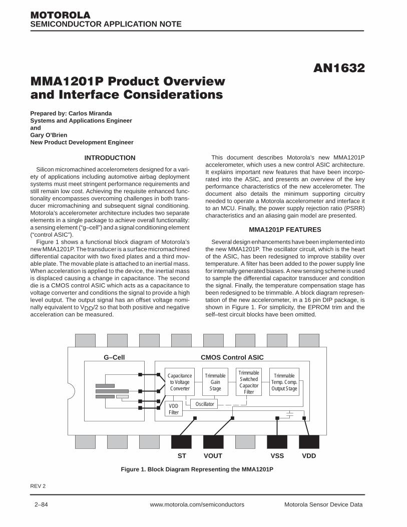
2–84 Motorola Sensor Device Datawww.motorola.com/semiconductors
Prepared by: Carlos MirandaSystems and Applications EngineerandGary O’BrienNew Product Development Engineer
INTRODUCTION
Silicon micromachined accelerometers designed for a vari-ety of applications including automotive airbag deploymentsystems must meet stringent performance requirements andstill remain low cost. Achieving the requisite enhanced func-tionality encompasses overcoming challenges in both trans-ducer micromachining and subsequent signal conditioning.Motorola’s accelerometer architecture includes two separateelements in a single package to achieve overall functionality:a sensing element (“g–cell”) and a signal conditioning element(“control ASIC”).
Figure 1 shows a functional block diagram of Motorola’snew MMA1201P. The transducer is a surface micromachineddifferential capacitor with two fixed plates and a third mov-able plate. The movable plate is attached to an inertial mass.When acceleration is applied to the device, the inertial massis displaced causing a change in capacitance. The seconddie is a CMOS control ASIC which acts as a capacitance tovoltage converter and conditions the signal to provide a highlevel output. The output signal has an offset voltage nomi-nally equivalent to VDD/2 so that both positive and negativeacceleration can be measured.
This document describes Motorola’s new MMA1201Paccelerometer, which uses a new control ASIC architecture.It explains important new features that have been incorpo-rated into the ASIC, and presents an overview of the keyperformance characteristics of the new accelerometer. Thedocument also details the minimum supporting circuitryneeded to operate a Motorola accelerometer and interface itto an MCU. Finally, the power supply rejection ratio (PSRR)characteristics and an aliasing gain model are presented.
MMA1201P FEATURES
Several design enhancements have been implemented intothe new MMA1201P. The oscillator circuit, which is the heartof the ASIC, has been redesigned to improve stability overtemperature. A filter has been added to the power supply linefor internally generated biases. A new sensing scheme is usedto sample the differential capacitor transducer and conditionthe signal. Finally, the temperature compensation stage hasbeen redesigned to be trimmable. A block diagram represen-tation of the new accelerometer, in a 16 pin DIP package, isshown in Figure 1. For simplicity, the EPROM trim and theself–test circuit blocks have been omitted.
G–Cell CMOS Control ASIC
Capacitanceto VoltageConverter
TrimmableGainStage
TrimmableSwitchedCapacitor
Filter
TrimmableTemp. Comp.Output Stage
VSS VDDVOUTST
VDDFilter
Oscillator
Figure 1. Block Diagram Representing the MMA1201P
SEMICONDUCTOR APPLICATION NOTE
REV 2

2–85Motorola Sensor Device Data www.motorola.com/semiconductors
• OscillatorThe oscillator has been redesigned to center the nominalfrequency within the trimming range and to have bettertemperature compensation. As shown in Figure 1, theoscillator controls three switched capacitor circuit sub–blocks within the ASIC, thus having direct impact on theirperformance. The trimmable oscillator enhances the con-trol of other performance parameters and enables the partto meet tighter specification tolerances. Additionally, theplacement of the oscillator on the silicon die has changed,contributing to a 50% reduction in the noise of the part.
• Power Supply FilterAn internal capacitor has been added between the VDD andVSS pins to provide some de–coupling of the power supply.Also, a lowpass filter has been added to the circuitry thatsupplies power to the transducer element and that sets theDC level of the capacitance–to–voltage converter stage.The filter response suppresses high frequency noise, butmaintains a ratiometric output.
• New Sensing SchemeThe capacitance–to–voltage converter employs innovativecircuit techniques (at the time of this writing, patents arepending) to improve signal ratiometricity. Amplification isachieved using an EPROM trimmable gain stage, provid-ing capability for both coarse and fine tuning. As in theprevious version of the control ASIC, the second gain stageis cascaded by a switched capacitor four pole Bessel low-pass filter, with a unity gain response and –3 dB frequencyat 400 Hz.
• Temperature CompensationThe final stage in the ASIC performs temperature com-pensation of gain. Thus, the temperature coefficient forsensitivity is set using EPROM trim.
PERFORMANCE ENHANCEMENTS
Motorola’s new MMA1201P accelerometer provides perfor-mance enhancements in a number of areas, including ratio-metric output, signal–to–noise ratio, output filter response,and temperature compensation. For complete details, refer tothe MMA1201P data sheet.
• Ratiometric OutputThe offset voltage and the sensitivity of the part are ratio-metric with supply voltage. Typical error values are lessthan 0.5%.
• Signal to Noise RatioThe noise has been reduced by 50% and is specified at3.5 mVRMS maximum. Typical values are about2.0 mVRMS. As a result, the signal to noise ratio of thepart is about 50 dB.
• Lowpass Filter ResponseThe frequency response of the four pole Bessel lowpassfilter has the –3 dB frequency at 400 Hz. The tolerance hasbeen narrowed by 60% and is specified at 40 Hz.
• Temperature CompensationThe sensitivity is very uniform over temperature, with typi-cal errors of about 1% over the specified temperaturerange. Also, although the spec allows for the equivalent of
5 mV/°C for the temperature coefficient of offset, typicalvalues are actually less than 2 mV/°C, at VDD equal to 5 V.
INTERFACE CONSIDERATIONS
With only four active pin connections, Motorola’s accel-erometers are very easy to use. There are only a few simpleconsiderations to be taken into account to ensure reliableoperation and attain the high level of performance that the canpart offer.
• Power SupplyPower is applied to the accelerometer through the VDD pin.For optimum performance, it is recommended that the partbe powered with a voltage regulator such as the MotorolaMC78L05. An optional 0.1 µF capacitor can be placed onthe VDD pin to complement the accelerometer’s internalcapacitor and provide additional de–coupling of the supply.The capacitor should be physically located as close aspossible to the accelerometer.
• GroundGround is applied through the VSS pin. Whenever pos-sible it is recommended that a solid ground plane be usedso that the impedance of the ground path is minimized. Ifthis is not possible, it is strongly recommended that a lowimpedance trace (no additional components should beconnected to it) be used to directly connect the VSS pin tothe power supply ground.
• Self–testThe ST pin is an active, high logic level input pin that pro-vides a way for the user to verify proper operation of thepart. It is pulled down internally. Therefore, for normaloperation, the user could apply a logic level “0” or leave itunconnected. Applying a logic level “1” to the ST pin willapply the equivalent of a 25 g acceleration to the trans-ducer, and the user should see a change in the outputequivalent to 25 times the part’s rated sensitivity.
• OutputThe accelerometer’s output is measured at the VOUT pin.As shown in Figure 1, the ASIC’s oscillator controls theswitched capacitor lowpass filter, with a nominal operatingfrequency of 65 kHz. As a result, a clock noise componentof about 2 mVpeak may be present at 65 kHz. Therefore, itis recommended that the user place a simple RC lowpassfilter on the VOUT pin to reduce the clock noise present inthe output signal. Recommended values are a 1 kΩ resistorand a 0.01 µF capacitor. These values produce a filter witha –3 dB frequency at about 16 kHz, which will not interferewith the response of the internal Bessel filter, yet will pro-vide sufficient attenuation (approximately –12 dB) of theclock noise.
Placing a filter on the output is especially recommended forapplications where the signal will be fed into a stand–aloneA/D converter, and in cases where the signal will be ampli-fied to a level where the amplified clock noise may begin tocontribute significantly to the noise floor of the system.However, if using an MCU or microprocessor in the system,the user may choose to use a software algorithm to digitallyfilter the signal, instead of using the analog RC filter. Thisoption would have to be evaluated based on the systemperformance requirements.

2–86 Motorola Sensor Device Datawww.motorola.com/semiconductors
• Connection to the A/D on an MCUWhen using the accelerometer with the analog to digitalconverter on an MCU, it is important to connect the supplyand ground pins of the accelerometer and the VRH and VRLpins of the MCU to the same supply and ground traces,respectively. This will maximize the ratiometricity of thesystem by avoiding voltage differences that may resultfrom trace impedances.
Figure 2 shows the recommended supporting circuitry for
operating the new accelerometer. Part (a) shows the16 pinDIP package version, the MMA1201P, while part (b) shows the6 pin Wingback package version, the MMA2200W. For theMMA1201P, pins 1, 2, 3, 6, 14, 15, and 16 have no internalconnections, and pins 9 through 13 are used for calibrationand trimming in the factory. These pins should all be left un-connected. For the MMA2200W, pins 1 and 4, and the wings(supporting pins) should be left unconnected.
VSS
ST
VDD VOUT
5
2
6 3
MMA2200W
VCC
C1
LOGIC INPUT R1
C2
OUTPUT SIGNAL
(b)
VSS
ST
VDD VOUT
7
4
8 5
MMA1201P
VCC
C1
0.1 F
LOGIC INPUT1k
R1
C2
OUTPUT SIGNAL
(a)
0.01 F
0.1 F
1k
0.01 F
Figure 2. Accelerometers with Recommended Supporting Circuitry
11 TRIM 3
PSRR AND ALIASING GAIN MODEL
Although the operational amplifiers in the MMA1201P’scontrol ASIC have a high power supply rejection ratio with afairly wide bandwidth, because the accelerometer is in realitya sampled analog system using switched capacitor technol-ogy, it is possible that when powered with a switching powersupply, noise from the supply will appear in the output signal.This is known as aliasing, the result being a signal with fre-quency equal to the difference between the frequency of thepower supply noise and the accelerometer’s sampling fre-quency. Aliasing gain is defined as the power of the outputsignal relative to an injected sinusoid on the VDD line poweringthe accelerometer.
Typical switching power supplies have operating frequen-cies between 50 and 100 kHz. The operating frequency of theaccelerometer’s switching capacitor circuitry is roughly 65kHz. Should the fundamental frequency of the switchingpower supply, or its harmonics, fall within 400 Hz of the ASIC’sfundamental frequency (or its harmonics), then any noisepresent in the power supply will be aliased into the passbandof the accelerometer. As will be explained later in this section,there are several simple ways to avoid aliasing.
As shown in Figure 1, there are many different signal pro-cessing stages in the ASIC. As a result, the aliasing gaincharacteristics of the part are a little bit more complex thanexplained in the previous paragraph. An analysis was done tocharacterize the worst case aliasing gain of the accelerome-ter. Devices from three production lots were used. The partswere tested at 105C with 5.25 V on VDD. The gain code wasset to the nominal value plus 4σ. Thus, the parts had a sensi-tivity that was approximately twice that of standard parts.Figure 3, shows a plot of the aliasing gain model that wasdeveloped. The model is based on the worst case results;typical parts should perform much better having much loweraliasing gain.
The following equation was used to fit the data and generatethe model:
Aliasing Gain = 1.6965 + 0.0029 * Freq. (kHz) + HRC1 * Freq. (kHz) + HRC2
where HRC1 and HRC2 are coefficients used in the model.Their values vary for each harmonic. Figure 4 lists the valuesof HRC1 and HRC2 for the fundamental frequency and the first5 harmonics.

2–87Motorola Sensor Device Data www.motorola.com/semiconductors
00
Fundamental 1st 2nd 3rd 4th 5th
SAMPLING FREQUENCY AND HARMONICS
ALIA
SIN
G G
AIN
(V/V
)
0.5
1
1.5
2
2.5
3
3.5
Figure 3. Worst Case Aliasing Gain Model Derived from Characterization Data
Harmonic Freq. (kHz) HRC1 HRC2 Aliasing Gain
Fundamental 65 0.0101 2.1120 0.4242
1st 130 0.0016 1.4881 0.3674
2nd 195 0.0237 4.1572 2.7116
3rd 260 0.0060 0.2919 0.6007
4th 325 0.0098 3.7439 3.2017
5th 390 0.0164 4.3054 0.7361
Figure 4. Values for Worst Case Aliasing Gain Model
The aliasing gain model can be used to estimate the amountof noise that can be expected on the output due to noise in theswitching power supply. As an example, consider a switchingpower supply operating at 65.05 kHz, with peak–to–peaknoise levels of 10, 6, 3.3, 2.5, 2, and 1.4 mV for the fundamen-tal and the first five harmonics, respectively. Assume the worst
case scenario, an almost perfect match of power supply fun-damental frequency with the fundamental of the ASIC and allnoise signals in phase. The power supply noise that would beseen at the output due to each harmonic would be calculatedas follows:
Harmonic Aliasing Gain P.S. Noise Output Noise
Fundamental 0.4242 10.00 mV 4.24 mV
1st 0.3674 6.00 mV 2.20 mV
2nd 2.7116 3.33 mV 9.04 mV
3rd 0.6007 2.50 mV 1.50 mV
4th 3.2017 2.00 mV 6.40 mV
5th 0.7361 1.40 mV 1.03 mV

2–88 Motorola Sensor Device Datawww.motorola.com/semiconductors
The total output noise would be the sum of the individualcomponents:
Total Output Noise = (4.24 + 2.20 + 9.04 + 1.50 + 6.40 + 1.03) mV
Total Output Noise = 24.41 mV peak–to–peak.
If this output signal were fed into an 8 bit A/D converter,referenced to 5 V full scale, the worst case error due to powersupply noise would be equivalent to 1 bit count.
The error that can occur in the output due to aliasing gaincan be avoided very easily. The easiest method is to power thepart with a voltage regulator. Since the voltage regulator pro-vides a clean, steady supply, the possibility of aliasing is elimi-nated. If the accelerometer is powered with a switching supply,a filter should be placed on the power supply output to elimi-nate the noise of the harmonics. If placing a filter on the switch-ing supply is not feasible, the user must ensure that theoperating frequency of the switching power supply is outsidethe frequency ranges of the peaks shown in Figure 3. The plotshown is a superposition of the response of the internal fourpole Bessel lowpass filter, scaled by the corresponding alias-ing gain for each harmonic. The Bessel filter has the –3 dBfrequency at 400 Hz and, being of fourth order, has a verysteep roll–off outside the passband, with approximately
–80 dB of attenuation at 4 kHz. If a switching power supplymust be used, its operating frequency should be at least 800Hz from the accelerometer’s sampling frequency. Any switch-ing noise present will be aliased to 800 Hz or higher, where theattenuation will be approximately –24 dB or lower, thus reduc-ing the power supply induced noise below the part’s noise floor.
CONCLUSION
The MMA1201P accelerometer demonstrates Motorola’scommitment to continuous product improvement. A new oscil-lator lowers the noise in the part and enables tighter control ofthe –3 dB bandwidth of the internal lowpass filter. The supplyvoltage is routed to the transducer and the DC level referenceof the capacitance–to–voltage converter stage through anewly added filter, thus reducing the part’s susceptibility topower supply noise. The capacitance–to–voltage converterstage uses new signal conditioning methods, which virtuallyeliminate ratiometric errors. The temperature compensationfor sensitivity is improved, producing a very flat response overtemperature. Overall the part offers much enhanced perfor-mance and is simpler to use. Equally important, Motorola’sMMA1201P accelerometer has remained very price competi-tive, making it ideal for most applications requiring accelera-tion sensors.

2–89Motorola Sensor Device Data www.motorola.com/semiconductors
Prepared by: Carlos Miranda, Systems and Applications Engineer andDavid Heeley, Systems and Applications Mechanical Engineer
INTRODUCTION
The Baseball Pitch Speedometer, in its simplest form, con-sists of a target with acceleration sensors mounted on it, anMCU to process the sensors’ outputs and calculate the ballspeed, and a display to show the result. The actual imple-mentation, shown in Figure 1, resembles a miniature pitchingcage, that can be used for training and/or entertainment. Thecage is approximately 6 ft. tall by 3 ft. wide by 6 ft. deep. Theupper portion is wrapped in a nylon net to retain the baseballsas they rebound off the target. A natural rubber mat, backedby a shock resistant acrylic plate, serve as the target. Accel-erometers, used to sense the ball impact, and buffers, used todrive the signal down the transmission line, are mounted onthe back side of the target. The remainder of the electronicsis contained in a display box on the top front side of the cage.
Accelerometers are sensors that measure the accelera-tion exerted on an object. They convert a physical quantityinto an electrical output signal. Because acceleration is avector quantity, defined by both magnitude and direction, anaccelerometer’s output signal typically has an offset voltageand can swing positive and negative relative to the offset,to account for both positive and negative acceleration. Anexample acceleration profile is shown in Figure 2. Becauseacceleration is defined as the rate of change of velocity withrespect to time, the integration of acceleration as a functionof time will yield a net change in velocity. By digitizing andnumerically integrating the output signal of an accelerometerthrough the use of a microcontroller, the “area under thecurve” could be computed. The result corresponds to the netchange in velocity of the object under observation. This is thebasic principle behind the Baseball Pitch Speedometer.
Figure 1. David Heeley, mechanical designer of the Baseball Pitch Speedometer Demo, tests his skills at Sensors Expo Boston ’97.
SEMICONDUCTOR APPLICATION NOTE
REV 1

2–90 Motorola Sensor Device Datawww.motorola.com/semiconductors
A
B
CAPTUREWINDOW
POINTOF
IMPACTTHRESHOLD
LEVEL
SYSTEM AT STEADY RATE
OSCILLATIONS THAT RESULTAS ENERGY IS DISSIPATED
Figure 2. Typical Crash Pattern for the Baseball Pitch Speedometer Demo
THEORY OF OPERATION
When a ball is thrown against the target, the accelerometersenses the impact and produces an analog output signal,proportional to the acceleration measured, resulting in a crashsignature. The amplitude and duration of the crash signatureis a function of the velocity of the ball. How can this crashsignature be correlated to the velocity of the baseball? Bymaking use of the principle of conservation of momentum (seeEquation 1). The principle of conservation of momentumstates that the total momentum within a closed systemremains constant. In our case, the system consists of thethrown ball and the target.
mball *Vball,initial + mtarget *Vtarget,initial =mball *Vball,final + mtarget *Vtarget,final Eq. 1
When the ball is thrown, it has a momentum equivalent tomball *Vball,initial. The target initially has zero momentumsince it is stationary. When the ball collides with the target,part of the momentum of the ball is transferred to the target,and the target will momentarily experience acceleration,velocity, and some finite, though small, displacement beforedissipating the momentum and returning to a rest state. The
other portion of momentum is retained by the ball as it bouncesoff the target, due to the elastic nature of the collision. Bymeasuring the acceleration imparted on the target, its velocityis computed through integration. Ideally, if the mass of the ball,the mass of the target, and the final velocity of the ball areknown, then the problem could be solved analytically and theinitial velocity of the baseball determined.
The analysis of the crash phenomenon is, however, actuallyquite complex. Some factors that must be taken into accountand that complicate the analysis greatly, are the springconstant and damping coefficient of the target. The target willbe displaced during impact because it is anchored to the frameby a thick rubber mat. This action effectively causes thesystem to have a certain amount of spring. Also, though themat is very dense, it will deform somewhat during impact andwill act as shock absorber. In addition, the ball itself also hasa spring constant and damping coefficient associated with it,since it bounces off the target and, though not noticeable bythe naked eye, will deform during the impact. Finally, and ofeven greater significance, the mass of the ball, the mass of thetarget, and the final velocity of the ball are neither known normeasured. So how can the system work?

2–91Motorola Sensor Device Data www.motorola.com/semiconductors
The Baseball Pitch Speedometer works by exploiting thefact that the final velocity of the target will be, according toEq. 1, linearly proportional to the initial velocity of the thrownball. Therefore, by measuring the acceleration response of thesystem to various ball velocities, which can be measured byindependent means such as a radar gun, the system could becalibrated and a linear model developed. To facilitate the char-acterization and calibration of the system, a pitching machinewas used to ensure that the incident ball speed would be
repeatable. It also eliminated potential error caused by thevariability of location of impact on the target that would inevit-ably result from several manual throws. Figure 3 shows alinear regression plot of the response of the system as a func-tion of incident velocity. As is indicated by the plot, just a simpleconstant of proportionality could be used to correlate the mea-sured acceleration response to the incident velocity of the ball,with fairly accurate results.
Figure 3. Baseball Pitch Speedometer Characterization Data
0 10 20 30 40 50 600
2000
4000
6000
8000
10000
12000
14000
BASEBALL SPEED AS RECORDED BY RADAR GUN (mph)
GR
AND
TO
TAL
AS R
ECO
RD
ED B
Y M
CU
YPREDICTED Y
IMPLEMENTATION — HARDWARE
The target mat of the Baseball Pitch Speedometer has anarea of approximately 9 ft2 (3 by 3). Even though the rubbermaterial used to construct the target is quite dense andheavy, the transmission of an impact is very poor if the ballstrikes the target too far from the sensor. Therefore, to cover
such a relatively large area it is necessary to use at leastfour devices; one centered in each quadrant of the squaretarget. In addition, a shock resistant plate about a quarterinch thick is mounted behind the rubber mat. These featureshelp make the response of the system more uniform andreduce errors that result from the variability of where the ballstrikes the target.

2–92 Motorola Sensor Device Datawww.motorola.com/semiconductors
The bulk of the circuit hardware is contained in a display boxmounted on the top front side of the cage. Since the accel-erometers are physically located far away from the motherboard (about 10 feet of wiring), op–amps were used to bufferthe accelerometers’ output and drive the transmission line.The four accelerometer signals are then simultaneously fedinto a comparator network and four of the ADC inputs on anMC68HC11 microcontroller. The MC68HC11 was selectedbecause it has the capability of converting four A/D channelsin one conversion sequence and operates at a higher clockspeed. These two features reduce the overall time intervalbetween digitizations of the analog signal (that result from theminimum required time for proper A/D conversion and fromsoftware latency) thus allowing a more accurate representa-tion of the acceleration waveform to be captured. Thecomparator network serves a similar purpose by eliminatingthe additional software algorithm and execution time thatwould be required to continually monitor the outputs of all fouraccelerometers and determine whether impact has occurredor not. By minimizing this delay (some is still present since theoutput signal must exceed a threshold, and a finite amount oftime is required for this) more of the initial and more significantpart of the signal is captured.
The comparator network employs four LM311’s configuredto provide an OR function, and a single output is fed into aninput capture pin on the MCU. A potentiometer and filtercapacitor are used to provide a stable reference thresholdvoltage to the comparator network. The threshold voltage isset as close as possible to the accelerometers’ offset voltageto minimize the delay between ball impact and the triggeringof the conversion sequence, but enough clearance must beprovided to prevent false triggering due to noise. Because thecomparator network is wired such that any one of the accel-erometer outputs can trigger it, the threshold voltage must behigher than the highest accelerometer offset voltage. Hystere-sis is not necessary for the comparator network, because
once the MCU goes into the conversion sequence it ignoresthe input capture pin.
The system is powered using a commercially available 9 Vsupply. A Motorola MC7805 voltage regulator is used to pro-vide a steady 5 Volt supply for the operation of the MCU, theaccelerometers, the comparator network, and the op–ampbuffers. The 9 V supply is directly connected to the commonanode 8–segment LED displays. Each segment can draw asmuch as 30 mA of current. Therefore, to ensure proper opera-tion, the power supply selected to build this circuit should becapable of supplying at least 600 mA. Ports B and C on theMCU are used to drive the LED displays. Each port output pinis connected via a resistor to the base of a BJT, which has theemitter tied to ground. A current limiting resistor is connectedbetween the collector of each BJT and the cathode of thecorresponding segment on the display. To minimize theamount of board space consumed by the output driving cir-cuitry, MPQ3904s (quad packaged 2N3904s) were selectedinstead of the standard discrete 2N3904s. The zero bit on PortC is connected to a combination BJT and MOSFET circuit thatdrives the “Your Speed” and “Best Speed” LED’s. The circuitis wired so that the LED’s toggle, and only one can be ON ata time.
Figure 4 shows a schematic of the circuit used. Part (a)shows the accelerometers, the op–amps used to buffer theoutputs and drive the transmission lines, the comparator net-work and the potentiometer used to set the detection thresh-old. Part (b) shows the MCU, with its minimal requiredsupporting circuitry. Part (c) shows the voltage regulator, amapping of the cathodes to the corresponding segments onthe LED displays, the BJT switch circuitry used to drive theseven segment display LEDs (although not shown on theschematic, this circuit block is actually repeated 15 times), andfinally, the circuitry used to drive the “Your Speed”/“BestSpeed” LEDs.
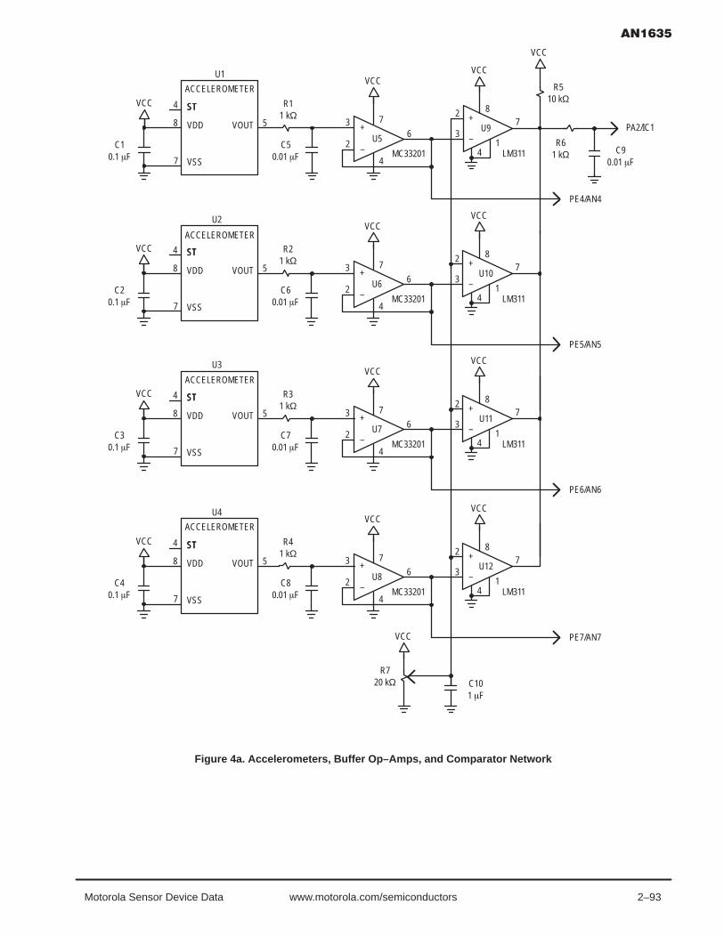
2–93Motorola Sensor Device Data www.motorola.com/semiconductors
Figure 4a. Accelerometers, Buffer Op–Amps, and Comparator Network
ST
ACCELEROMETER
STST
VDD
VSS
VOUT
U1
4
8
7
VCC
C10.1 F
5
R11 kΩ
C50.01 F
+
–U5
3
2
4
7
VCC
MC33201
6
+
–U9
2
3
8
VCC
VCC
R510 kΩ
R61 kΩ
PA2/IC1
C90.01 F
PE4/AN4
41
LM311
7
STSTST
VDD
VSS
VOUT
U2
4
8
7
VCC
C20.1 F
5
R21 kΩ
C60.01 F
+
–U6
3
2
4
7
VCC
MC33201
6
+
–U10
2
3
8
VCC
PE5/AN5
41
LM311
7
STSTST
VDD
VSS
VOUT
U3
4
8
7
VCC
C30.1 F
5
R31 kΩ
C70.01 F
+
–U7
3
2
4
7
VCC
MC33201
6
+
–U11
2
3
8
VCC
PE6/AN6
41
LM311
7
STSTST
VDD
VSS
VOUT
U4
4
8
7
VCC
C40.1 F
5
R41 kΩ
C80.01 F
+
–U8
3
2
4
7
VCC
MC33201
6
+
–U12
2
3
8
VCC
PE7/AN7
41
LM311
7
C101 F
VCC
R720 kΩ
ACCELEROMETER
ACCELEROMETER
ACCELEROMETER

2–94 Motorola Sensor Device Datawww.motorola.com/semiconductors
Figure 4b. MC68HC11E9 MCU with Supporting Circuitry
VCC
8 MHz
R11 10 M
R151 k
VCC
R12 4.7 k
R13 4.7 k
VCC
IN RST*
MC34164P
GND
12
3
U13
C14
18 pF
C130.1
VCC VCC
PA2/IC1
PE7/AN7
PE4/AN4PE5/AN5PE6/AN6
R14 4.7 k
VRL
VRH
MODA/LIR*
MODB/VSTBY
IRQ*
XIRQ*
RESET*
XTAL
EXTAL
VSS
VDD
PE7/AN7PE6/AN6PE5/AN5PE4/AN4PE3/AN3PE2/AN2PE1/AN1PE0/AN0
PD5/SS*PD4/SCK
PD3/MOSIPD2/MISO
PD1/TxDPD0/RxD
PC7/AD7PC6/AD6PC5/AD5PC4/AD4PC3/AD3PC2/AD2PC1/AD1PC0/AD0
STRA/AS
STRB/R/W*
PB7/A15PB6/A14PB5/A13PB4/A12PB3/A11PB2/A10PB1/A9PB0/A8
PA7/PAI/OC1PA6/OC2/OC1PA5/OC3/OC1PA4/OC4/OC1
PA3/IC4/OC5/OC1PA2/IC1PA1/IC2PA0/IC3
E
MC68HC11E9
51
52
3
2
8
7
1
26
5048464449474543
252423222120
161514131211109
4
6
3536373839404142
2728293031323334
5
17
18
19
U14
1
C16
C124.7
“Your’’ / “Best’’FGEDCBA
FGEDCB A
DP4.7 k
R10
R9200 k
R84.7 k
RESET1C11
Ones DigitLED Display
Tens DigitLED Display
µF µF
µF
µF
Ω
ΩΩ
Ω
Ω
Ω
Ω
Ω
18 pF
C15

2–95Motorola Sensor Device Data www.motorola.com/semiconductors
VIN VOUTMC78L05ACP
GND
1
2
3
U15
+9 VDC P.S. VCC
B+
1C17 C18
GND P.S.
R16 – R3010 k
R32 – R46180
B+
From PB or PC
1/8 LED Display
U16–U19 MPQ3904
R3110
R47
PB0
VCC
R481
VCC
“Your Speed’’
“Best Speed’’
1/4 MPQ3094
U20 VN0300L
B
C
D
E
F
G
DP
µF 1µF
A
Ω
Ω
Ωk
1 Ωk
Ωk
Figure 4c. Voltage Regulator, LED Segment Mapping, and LED Driving Circuitry

2–96 Motorola Sensor Device Datawww.motorola.com/semiconductors
IMPLEMENTATION — SOFTWARE
The operation of the Baseball Pitch Speedometer is verysimple. Upon power on reset, the output LEDs are initializedto display “00” and “Best Speed.” The analog to digital con-verter is turned on and the offset voltages of the accelerome-ters are measured and stored. Finally, all the variables areinitialized and the MCU goes into a dormant state, where it willwait for a negative edge input capture pulse to trigger it tobegin processing the crash signal.
Once the input capture flag is set, the MCU will immediatelybegin the analog to digital conversion sequence. As it digitizesthe crash signature, it will calculate the absolute differencebetween the current value and the stored offset voltage value.It will integrate by summing up all the differences. Figure 2shows a typical crash signature of the Baseball PitchSpeedometer. As illustrated, starting at the point of impact (A),the acceleration will initially ramp up, reaching a maximum,then decrease as the target is displaced. Because the targetis constrained to the frame structure, the acceleration willcontinue to decrease until it reaches a minimum (point B),which correspond to the travel stop of the target. It is difficultto determine exactly when point B will occur, because theamplitude and duration of the initial acceleration pulse will varywith ball speed. Therefore, the capture window duration is setso that it will encompass most typical crash signatures, whilerejecting most of the secondary ripples that result as theenergy is dissipated by the system.
After integrating the four signals, the results are addedtogether to produce an overall sum. This procedure averagesout the individual responses and reduces measurement errordue to the variability of where the ball lands on the target. TheMCU then divides the grand sum by an empirically predeter-mined constant of proportionality. The result will then gothrough a binary to BCD conversion algorithm. A look–up tableis used to match the BCD numbers to their corresponding7–segment display codes. The calculated speed is displayedon the two digit 8–segment displays (one segment corre-sponds to the decimal point), and the “Your Speed” LED is
turned on while the “Best Speed” LED is turned off. After aduration of approximately five seconds, the LEDs are toggledand stored best speed is redisplayed. The five second delayis used to provide enough time for the user to check his/herspeed and also to allow the target to return to a rest state. Thesystem is now ready for another pitch. A complete listing of thesoftware is presented in the Appendix.
CONCLUSION
The Baseball Pitch Speedometer works fairly well, with anaccuracy of +/– 5 mph. The dynamic range of the system isalso worthy of note, measuring speeds from less than 10 mphup to well above the 70 mph range. One key point to empha-size, is that the system is empirically calibrated, and so tomaintain good accuracy the system should only be used withballs of mass equal to those used during calibration.
Although intended mainly for training and recreational pur-poses, the Baseball Pitch Speedometer demonstrates a veryimportant concept concerning the use of accelerometers.Accelerometers can be used not only to detect that an eventsuch as impact or motion has occurred, but more importantlythey measure the intensity of such events. They can be usedto discern between different crash levels and durations. Thisis very useful in applications where it is desired to have thesystem respond in accord with the magnitude of the inputbeing monitored. An example application would be a smartair bag system, where the speed at which the bag inflates isproportional to the severity of the crash. The deployment rateof the airbag would be controlled so that it does not throw theoccupant back against the seat, thus minimizing the possibil-ity of injury to the occupant. Another application where thisconcept may be utilized is in car alarms, where the responsemay range from an increased state of readiness and monitor-ing, to a full alarm sequence depending on the intensity of theshock sensed by the accelerometer. This could be used toprevent unnecessary firing of the alarm in the event that ananimal or person were to inadvertently bump or brush againstthe automobile.

2–97Motorola Sensor Device Data www.motorola.com/semiconductors
APPENDIX — ASSEMBLY CODE LISTING FOR BASEBALL PITCH SPEEDOMETER
* Baseball Pitch Speedometer – Rev. 1.0** Program waits for detection of impact via the input capture pin and then reads four A/D channels.* The area under the Acceleration vs. Time curve is found by subtracting the steady state offsets* from the digitized readings and summing the results. The sum is then divided by an empirically* determined constant of proportionality, and the speed of the ball is displayed.** Written by Carlos Miranda* Systems and Applications* Sensor Products Division* Motorola Semiconductor Products Sector* May 6, 1997*********************************************************************************************************** Although the information contained herein, as well as any information provided relative ** thereto, has been carefully reviewed and is believed accurate, Motorola assumes no ** liability arising out of its application or use, neither does it convey any license under ** its patent rights nor the rights of others. ********************************************************************************************************** These equates assign memory addresses to variables.EEPROM EQU $B600CODEBGN EQU $B60DREGOFF EQU $1000 ;Offset to access registers beyond direct addressing range.PORTC EQU $03PORTB EQU $04DDRC EQU $07TCTL2 EQU $21TFLG1 EQU $23ADCTL EQU $30ADR1 EQU $31ADR2 EQU $32ADR3 EQU $33ADR4 EQU $34OPTION EQU $39STACK EQU $01FF ;Starting address for the Stack Pointer.RAM EQU $0000* These equates assign specific masks to variables to facilitate bit setting, clearing, etc.ADPU EQU $80 ;Power up the analog to digital converter circuitry.CSEL EQU $40 ;Select the internal system clock.CCF EQU $80 ;Conversion complete flag.IC1F EQU $04 ;Input Capture 1 flag.IC1FLE EQU $20 ;Configure Input Capture 1 to detect falling edges only.IC1FCLR EQU $FB ;Clear the Input Capture 1 flag.CHNLS47 EQU $14 ;Select channels 4 through 7 with MULT option ON.SAMPLES EQU $0200 ;Number of A/D samples taken.OC1F EQU $80 ;Output Compare 1 flag.OC1FCLR EQU $7F ;Clear the Output Compare flag.CURDLY EQU $0098 ;Timer cycles to create delay for displaying ”Your Speed.”RAMBYTS EQU $19 ;Number of RAM variables to clear during initialization.ALLONES EQU $FFYOURSPD EQU $01PRPFCTR EQU $00AD ;This constant of proportionality was empirically determined.* Variables used for computation.
ORG RAMOFFSET1 RMB 1 ;One for each accelerometer.OFFSET2 RMB 1OFFSET3 RMB 1OFFSET4 RMB 1SUM1 RMB 2 ;Area under the acceleration vs. time curve.SUM2 RMB 2SUM3 RMB 2SUM4 RMB 2GRNDSUM RMB 2COUNT RMB 2CURBIN RMB 1TEMPBIN RMB 1BCD RMB 2CURDSPL RMB 2MAXBIN RMB 1MAXDSPL RMB 2* LED seven segment display patterns table.
ORG EEPROMJMP START
SEVSEG FCB %11111010FCB %01100000FCB %11011100FCB %11110100FCB %01100110FCB %10110110FCB %10111110FCB %11100000FCB %11111110FCB %11100110

2–98 Motorola Sensor Device Datawww.motorola.com/semiconductors
* This is the main program loop.ORG CODEBGN
START LDS #STACKLDX #REGOFFJSR LEDINITJSR ADCINITJSR VARINIT
MAIN JSR CAPTUREJSR COMPUTEJSR BINTBCDJSR OUTPUTBRA MAIN
* This subroutine initializes ports B & C, and the LED display.LEDINIT PSHX
PSHALDX #REGOFFBSET DDRC,X,ALLONES ;Configure port C as an output.LDAA SEVSEGSTAA PORTB,XSTAA PORTC,XPULAPULXRTS
* This subroutine initializes the analog to digital converter.ADCINIT PSHX
PSHALDX #REGOFFBSET OPTION,X,ADPU ;Turn on A/D converter via ADPU bit.BCLR OPTION,X,CSEL ;Select system e clock via CSEL bit.CLRA
DELAY INCABNE DELAYPULAPULXRTS
* This subroutine clears all the memory variables.VARINIT PSHX
LDX #$0000CLRVAR CLR OFFSET1,X
INXCPX #RAMBYTS ;Number of RMB bytes.BLO CLRVAR
DONECLR LDX #REGOFFLDAA #CHNLS47 ;Measure the offset.STAA ADCTL,X
OFSWAIT BRCLR ADCTL,X,CCF,OFSWAITLDD ADR1,XSTD OFFSET1LDD ADR3,XSTD OFFSET3PULXRTS
* This subroutine waits for impact and computes the area under the curve.CAPTURE PSHX
PSHAPSHBLDX #REGOFFBSET TCTL2,X,IC1FLE ;Set IC1 to detect falling edge only.BCLR TFLG1,X,IC1FCLR
MONITOR BRCLR TFLG1,X,IC1F,MONITORADCREAD LDAA #CHNLS47 ;Select channels 4 – 7 for conversion.
STAA ADCTL,XADCWAIT BRCLR ADCTL,X,CCF,ADCWAITCALDLT1 LDAB ADR1,X
SUBB OFFSET1BPL ADDSUM1COMBINCB
ADDSUM1 CLRAADDD SUM1STD SUM1
CALDLT2 LDAB ADR2,XSUBB OFFSET2BPL ADDSUM2COMBINCB
ADDSUM2 CLRAADDD SUM2STD SUM2
CALDLT3 LDAB ADR3,XSUBB OFFSET3BPL ADDSUM3COMBINCB

2–99Motorola Sensor Device Data www.motorola.com/semiconductors
ADDSUM3 CLRAADDD SUM3STD SUM3
CALDLT4 LDAB ADR4,XSUBB OFFSET4BPL ADDSUM4COMBINCB
ADDSUM4 CLRAADDD SUM4STD SUM4LDD COUNTADDD #$0001STD COUNTCPD #SAMPLESBLO ADCREADPULBPULAPULXRTS
* This subroutine computes the ball speed by dividing the overall sum by a constant.COMPUTE PSHX
PSHAPSHBLDD SUM1ADDD SUM2ADDD SUM3ADDD SUM4STD GRNDSUMLDX #PRPFCTRIDIVXGDXSTAB CURBINPULBPULAPULXRTS
* This subroutine converts from binary to BCD. (Limited to number up to 99 decimal.)BINTBCD PSHX
PSHAPSHBLDX #$0000LDAA CURBINSTAA TEMPBINCLRACLRB
BINSHFT LSL TEMPBINROLBLSLACMPB #$10BLO CHKDONEINCAANDB #$0F
CHKDONE INXCPX #$0008BEQ RAILAT9
CHKFIVE CMPB #$05BLO BINSHFTADDB #$03BRA BINSHFT
RAILAT9 CMPA #$09 ;Force the display to “99” if speed > 100 mph.BLS DONELDD #$0909
DONE STD BCDLDX #SEVSEG ;This part finds the seven segment display codes.XGDXADDB BCDXGDXLDAA $00,XSTAA CURDSPLLDX #SEVSEGXGDXADDB BCD+1XGDXLDAA $00,XSTAA CURDSPL+1PULBPULAPULXRTS
* This subroutine displays the current speed for 5 seconds & then displays the maximum.OUTPUT PSHX
PSHAPSHB

2–100 Motorola Sensor Device Datawww.motorola.com/semiconductors
LDX #REGOFFLDAA CURBINCMPA MAXBINBLS OLDMAXSTAA MAXBINLDD CURDSPLSTD MAXDSPL
OLDMAX LDD CURDSPLSTD PORTC,XBSET PORTB,X,YOURSPD ;Toggle the ”YOUR”/“BEST” LEDs.LDD #$0000
LEDWAIT BCLR TFLG1,X,OC1FCLR ;Clear output compare 1 flag.DSPLDLY BRCLR TFLG1,X,OC1F,DSPLDLY
ADDD #$0001CPD #CURDLY ;Decimal 152. (152 * 33ms = 5.0 sec)BLO LEDWAITLDX #$0000
RECLEAR CLR SUM1,X ;Clear 12 RAM bytes beginning at address ”SUM1”.INX ;Clears SUM1 thru SUM4, GRNDSUM, and COUNT.CPX #$000CBLO RECLEARLDX #REGOFFLDD MAXDSPLSTD PORTC,X ;The ”YOUR”/“BEST” LEDS are automatically toggled.PULBPULAPULXRTS

2–101Motorola Sensor Device Data www.motorola.com/semiconductors
Prepared by Brandon Loggins
Automobile manufacturers require all system electronics topass stringent electromagnetic compatibility (EMC) tests.Airbag systems are one of the systems that must performadequately under EMC tests. There are different types of testsfor EMC, one of which is testing the tolerance of the systemto high frequency conducted emissions. One of the moststringent methods for EMC evaluation is the Bulk CurrentInjection (BCI) test. The entire airbag system must continue tofunction normally throughout the BCI test. This applicationnote will discuss how to reduce susceptibility to BCI for theMotorola accelerometer but the information presented herecan be applied to other electronic components in the system.
BCI TEST SETUP
The BCI test procedure follows a published SAE engineering
standard, “Immunity to Radiated Electric Fields ~ Bulk CurrentInjection (BCI)”, or SAE J 1113/401. For an airbag module, thisinvolves injecting the desired current into the wiring harness bycontrolling current in the injection probe. The test frequency canvary from one to several hundred MHz. There are at least 20frequency steps per octave required for the test, but as manyas 50 steps per octave can be used. The injection probe isplaced on the harness in one of three distances from the airbagmodule connector: 120, 450 and 750 mm. There is a monitorpickup probe present to measure the amount of current beinginjected. It is placed 50 mm from the airbag module. This feedsback to the system to ensure that the desired test current isbeing injected on to the wiring harness. Figure 1 shows thesetup for the BCI test. (For more details, see the SAE J1113/401 Test Procedure).
Figure 1. BCI Test Setup
ANECHOIC CHAMBER WALL
PCLOAD BOX
INJECTIONPROBE
PICKUPPROBE
WIRING HARNESS
AIRBAGMODULE
70, 450, or 750 mm
50 mm
BASEPLATE CONNECTEDTO GROUND
The harness connects the airbag module to a load box. Thisload box provides simulated loads for terminating theremainder of the airbag system (firing ignitors, etc.). The datacoming back is translated from J1850 to RS232 to becommunicated to a dummy terminal on a PC. For safetyreasons, this test is typically performed inside an anechoicchamber to shield high frequency emissions from equipmentand humans.
BCI TEST PROCEDURE FOR THEMMA2202D ACCELEROMETER
The accelerometer is evaluated in the following manner. Inan airbag system, the microcontroller’s A/D converter digitizesthe accelerometer output. The microcontroller sends thisvalue to the communication ASIC which translates the logicfrom board level logic to RS232, then sends the value back
SEMICONDUCTOR APPLICATION NOTE
REV 2

2–102 Motorola Sensor Device Datawww.motorola.com/semiconductors
along the wiring harness. Once through the chamber wall, thedata is translated to RS232 and fed to a dummy terminal. Onthe terminal screen, the A/D codes for the accelerometer canbe monitored for unexpected performance.
Ideally, when the accelerometer is at rest (no accelerationapplied), the output should be at 0g, regardless of what EMCtesting the system may be subjected to. Depending on thecrash algorithm of the airbag module software, there is someallowable offset shift that can be tolerated. Higher shift inoutput could create errors in the crash analysis software,perhaps causing the airbags to unnecessarily deploy whenthere is not a crash or not deploy when there is a crash.
The Motorola accelerometer must be able to meet theairbag system requirements throughout BCI exposure. It hasa sensitivity of 40 mV/g and an offset (0g output) of 2.50 V.During the BCI test, the accelerometer output should be2.50 V at 0g with as little drift as possible. A typical airbagsystem may have software that can tolerate from as little as0.5 g up to 2.0 g. of deviation from the offset. The system wouldthen expect the accelerometer output to be within 40 mV of theoffset during the entire BCI test. Therefore, at any given
frequency of the BCI test, if the output deviates outside thisexpected window of drift, it fails the test.
MMA2202D ACCELEROMETER BCI TESTRESULTS
If a system has not been well designed for electromagneticcompatibility, the accelerometer, as well as other devices, canhave performance problems. What has been found for theaccelerometer is that in some system applications, it suffersfrom an offset shift when certain frequencies of BCI areapplied. For example, in one airbag system being tested at acertain frequency, with the desired BCI current applied, theoffset is found to shift down by 60 mV. This would equate to anerror of 1.5 g. See Figure 2. At other frequencies, this shift iseven higher. This DC shift plot was taken with an oscilloscopeusing a 20 MHz filter to remove the high frequency componentof the signal. Probes are placed at the accelerometer in thesystem application. The plot shows the accelerometer outputbefore and after BCI was applied (before and after the RFgenerator creating the high frequency signal was turned on).
Figure 2. Accelerometer Tested Under High Frequency BCI
ACCELEROMETER VOUTw/o BCI ACCELEROMETER VOUT
w/BCI
VCC
This phenomenon has been determined to be system levelrelated. PCB layout and grounding for the accelerometer willaffect its performance. This was found by testing theaccelerometer outside of the airbag module. The device wasput on a test board by itself with only the supply decouplingcapacitor of 0.1 µF connected to it. To simulate the effect ofBCI on Vcc, a frequency generator was used to inject a knownhigh frequency sinusoid that caused BCI failure on to the 5.0 Vsupply voltage. The device was first tested in small test boardwith ground provided by one wire back to the supply. Thisgrounding reproduced the failure due to BCI seen at the
module level. The test board was then mounted down to aground plane provided by a copper plate and theaccelerometer ground was soldered to the plate (providing alow impedance path to ground). With this setup, the offset shiftdid not occur.
If a system does not incorporate a good PCB layoutproviding a low impedance to ground, the accelerometeroutput may shift at certain high frequencies. This output offsetshift was caused by a shift in the 0–5 V supply window.Because the accelerometer has a ratiometric output, its offsetis dependent on the supply voltage. Any change in the supply

2–103Motorola Sensor Device Data www.motorola.com/semiconductors
voltage will result in the same proportional change in theoutput. For example, if the 5 V supply were to change by 10%,from 5.0 V to 5.5 V, the accelerometer offset will change by10% also, from 2.5 V to 2.75 V. This phenomena would alsooccur if the ground were to shift. A 100 mV change in groundwould result in a 50 mV change in the output. If theaccelerometer does not have low impedance path to groundand parasitics from a poor ground are present as a result, theground seen by the accelerometer may change overfrequency. So, during a BCI test, if the 5.0 V supply does notshift but the output of the accelerometer does, the ground tothe accelerometer may be moving.
It was found with some experimentation that the offset shiftcan be eliminated with proper board layout techniques asdescribed below.
PROPER LAYOUT TECHNIQUES
Since the Motorola accelerometer is a sensitive analogdevice that relies on a clean supply to function withinestablished parameters, there are some techniques that canbe employed to minimize the effects of BCI on theaccelerometer performance. PCB layout is paramount toreducing susceptibility to BCI.
• A low impedance path to ground will provide shunting of thehigh frequency interference and minimize its effect on theaccelerometer. The best way to provide a good path is byputting a solid, unbroken ground plane in the PCB. Thisground plane should be shunted to chassis ground at themodule connector. This will ensure that the high frequencyBCI will be shunted before interfering with accelerometerperformance.
• All accelerometer pins that require ground connectionshould be tied together to a common ground.
• Traces attached directly to the connector pins can receivehigh RF noise, which can couple to nearby traces and com-ponents. Increasing series impedance of the traces helpsreduce the couple or conducted noise. High frequency fil-ters on the supply line and other susceptible lines may berequired to filter out high frequency interference introducedby the BCI test. Signal lines that carry low current can toler-ate series resistances of 100–200 Ω.
• Decoupling capacitors on every input line to the commonground plane will help shunt the high frequency away fromthe system. These should be placed near the connector.
• Signal trace lengths to and from the accelerometer shouldbe kept at a minimum. The shorter the trace, the lesschance it has of picking up high frequency BCI signals asit crosses the board. Trace lengths can be reduced by plac-ing the accelerometer and the microcontroller as closetogether as possible. Signal and ground traces loopingshould be minimized.
• A decoupling capacitor on the accelerometer Vcc pin willalso help minimize BCI effects. The recommended value is0.1 µF. This capacitor should be placed as close as pos-sible to the accelerometer to achieve the best results.
• To maximize ratiometricity, the accelerometer Vcc and themicrocontroller A/D reference pin should be on the sametrace. The accelerometer ground and the microcontrollerground should also share the same ground point. There-fore, when there is signal interference due to BCI, the A/Dconverter and the accelerometer will see the interferenceat the same level. This will result in the same digital coderepresentation of acceleration without signal interference.
• A clean power supply to both the accelerometer and themicrocontroller should be provided. Supply traces shouldavoid high current traces that might carry high RF currentsduring the BCI test. The traces should be as short aspossible.
• The accelerometer should be placed on the opposite endof the PCB away from the connector. The farther the dis-tance, the lower the chance high frequency RF from BCIwill interfere with the accelerometer.
• The accelerometer should be placed away from high cur-rent paths that may carry high RF currents during the BCItest.
Automotive customers will continue to require airbagsystems to have high standards for EMC. One way to test forEMC is perform the Bulk Current Injection test. Because of thehigh current involved, BCI is one of the most difficult EMC teststo pass. Being part of the airbag system, the accelerometermust continue to function normally under application of highfrequency BCI. The accelerometer is highly sensitive toplacement on the board and its connection to ground. Poordesign will caused the device to fail the BCI test. The practiceof good PCB layout, device placement and good groundingwill allow the accelerometer to function within specificationand pass the BCI test.

2–104 Motorola Sensor Device Datawww.motorola.com/semiconductors
Prepared by: Leticia Gomez and Raul FigueroaSensor Products DivisionSystems and Applications Engineering
INTRODUCTIONThis application note describes the Motorola Accelerometer
Evaluation Board (Figure 1). The Accelerometer EvaluationBoard is a small circuit board intended to serve as an aid insystem design with the capability for mounting the followingdevices: MMA1220D, MMA1201P, MMA1200D, MMA2201D.This evaluation board is useful for quickly evaluating any ofthese three devices. It also provides a means forunderstanding the best mounting position and location of anaccelerometer in your product.
CIRCUIT DESCRIPTIONFigure 2 is a circuit schematic of the evaluation board. The
recommended decoupling capacitor at the power source andrecommended RC filter at the output, are included on theevaluation board. This RC filter at the output of theaccelerometer minimizes clock noise that may be presentfrom the switched capacitor filter circuit. No additionalcomponents are necessary to use the evaluation board.
Refer to the respective datasheet of the device being usedfor specifications and technical operation of theaccelerometer.
The evaluation board has a 4–pin header (J1 in Figure 1) forinterfacing to a 5 volt power source or a 9 to 15 volt power
source (for example, 9 V battery). Jumper JP1 (see Figure 1)must have the following placement: on PS if a 5 V supply isbeing used or on BATT if a 9 V to 15 V supply is used. A 5 Vregulator (U1 in figure 1) supplies the necessary power for theaccelerometer in the BATT option.
The power header also provides a means for connecting tothe accelerometer analog output through a wire to anotherbreadboard or system. Four through–hole sockets areincluded to allow access to the following signals: VDD, GND,ST and STATUS. These sockets can be used as test points oras means for connecting to other hardware.
The ON/OFF switch (S1) provides power to theaccelerometer and helps preserve battery life if a battery isbeing used as the power source. S1 must be set towards the“ON” position for the accelerometer to function. The greenLED (D1) is lit when power is supplied to the accelerometer.
A self–test pushbutton (S2) on the evaluation board is aself–test feature that provides verification of the mechanicaland electrical integrity of the accelerometer. The STATUS pinis an output from the fault latch and is set high if one of the faultconditions exists. A second pressing of the pushbutton (S2)resets the fault latch, unless of course one or more faultconditions continue to exist.
Figure 1. Motorola Accelerometer Evaluation Board
Jumper (JP1) 5 V Regulator
Power Header
On/Off Switch(S1)
Power LED (D1)Test Points
Self–TestPushbutton (S2)
MMA Device
MountingHole (1 of 4)
(U1)PS
BATT
STATUS
(J1)
Accelerometer Output(Vout)
SEMICONDUCTOR APPLICATION NOTE
REV 0

2–105Motorola Sensor Device Data www.motorola.com/semiconductors
Figure 2. Evaluation Board Circuit Schematic
.01 FC3
.01 FC4
.1 FC1
9 V to 15 VJ1
3
MC78L05
IN OUTGND
1
.33 FC2
BATT
+5 VJ1
750R1
PS
JP1
ON
S1
D1Green LED
VDD
STATUS
VSS
7
6 STATUS
TP2
VOUT5
MMA1220D
ST
S2
1K
R2
4J1
VOUT
TP3
OFF
82 VDD
VDD
VOUT
Figure 3. Motorola Accelerometer Evaluation Board with Test Socket
Pin 1
20–pinTest Socket
MMA Device
Bottom Lid Snap
Unused pins
SOIC
The board allows for direct mounting of a 16–pin DIP orSOIC package. For the SOIC device, a 20–pin test socket isused to allow for evaluation of more than one device withoutsoldering directly to the board and potentially damaging thePCB. Care must be taken in placing the device correctly in thesocket as four pins of the socket will not be used. With theboard oriented as shown in Figure 3, Pin 1 should facedownward and the device should be positioned toward the topof the test socket, thereby exposing the bottom four pins of thetest socket. The socket is marked to help identify the 4 unusedsocket pins. Lids to secure the device in the socket areincluded with the board and delicately snap into place. The lids
can be removed by applying pressure to the sides of the lid orby lifting the top and bottom snaps of the lid.
PIN OUT DESCRIPTION
Pin Name Description
4 ST Logic input pin to initiate self–test
5 VOUT Output voltage of the accelerometer
6 STATUS Logic output pin to indicate fault
7 VSS Power supply ground
8 VDD Power supply input

2–106 Motorola Sensor Device Datawww.motorola.com/semiconductors
BOARD LAYOUT AND CONTENTFigures 4 and 5 show the layout used on the evaluation
board. Through–hole mounting components have beenselected to facilitate component replacement.
MOUNTING CONSIDERATIONSSystem design and sensor mounting can affect the
response of a sensor system. The placement of the sensoritself is critical to obtaining the desired measurements. It isimportant that the sensor be mounted as rigidly as possible toobtain accurate results. Since the thickness and mounting ofthe board varies, parasitic resonance may distort the sensormeasurement. Hence, it is vital to fasten and secure to thelargest mass structure of the system, i.e. the largest truss, thelargest mass, the point closest to source of vibration. On theother hand, dampening of the sensor device can absorb muchof the vibration and give false readings as well. The evaluationboard has holes on the four corners of the board for mounting.
It is important to maintain a secure mounting scheme tocapture the true motion.
Orientation of the sensor is also crucial. For best results,align the sensitive axis of the accelerometer to the axis ofvibration. In the case of the MMA1220D, the sensitive axis isperpendicular to the plane of the evaluation board.
SUMMARYThe Accelerometer Evaluation Board is a design–in tool for
customers seeking to quickly evaluate an accelerometer interms of output signal, device orientation, and mountingconsiderations. Both through–hole and surface mountpackages can be evaluated. With the battery supply optionand corner perforations, the board can easily be mounted onthe end product; such as a motor or a piece of equipment.Easy access to the main pins allows for effortless interfacingto a microcontroller or other system electronics. The simplicityof this evaluation board provides reduced development timeand assists in selecting the best accelerometer for theapplication.
Figure 4. Board La yout (Component Side ) Figure 5. Board La yout (Back Side )

2–107Motorola Sensor Device Data www.motorola.com/semiconductors
Case Outlines
CASE 475–01ISSUE B
16 LEAD SOIC
NOTES:1. ALL DIMENSIONS ARE IN MILLIMETERS.2. INTERPRET DIMENSIONS AND TOLERANCES
PER ASME Y14.5M, 1994.3. DIMENSIONS ”A” AND ”B” DO NOT INCLUDE
MOLD FLASH OR PROTRUSIONS. MOLD FLASHOR PROTRUSIONS SHALL NOT EXCEED 0.15PER SIDE.
4. DIMENSION ”D” DOES NOT INCLUDE DAMBARPROTRUSION. PROTRUSIONS SHALL NOTCAUSE THE LEAD WIDTH TO EXCEED 0.75
DIM MIN MAXMILLIMETERS
A 10.15 10.45B 7.40 7.60C 3.30 3.55D 0.35 0.49F 0.76 1.14G 1.27 BSCJ 0.25 0.32K 0.10 0.25M 0 7 P 10.16 10.67R 0.25 0.75
1 8
16 9
P
2 PLACES, 16 TIPS
D16X
A0.15 BT
AM0.13 BT
C
K
R X 45
J
FM
SEATINGPLANE
A
B
A
B
T
G
G/2
0.1
CASE 475A–01ISSUE O
20 LEAD SOIC
NOTES:1. DIMENSIONING AND TOLERANCING PER ANSI
Y14.5M, 1982.2. CONTROLLING DIMENSION: MILLIMETER.3. DIMENSIONS A AND B DO NOT INCLUDE MOLD
PROTRUSION.4. MAXIMUM MOLD PROTRUSION 0.15 (0.006) PER
SIDE.5. DIMENSION D DOES NOT INCLUDE DAMBAR
PROTRUSION. ALLOWABLE DAMBARPROTRUSION SHALL BE 0.13 (0.005) TOTAL INEXCESS OF D DIMENSION AT MAXIMUMMATERIAL CONDITION.
DIM MIN MAX MIN MAXINCHESMILLIMETERS
A 12.67 12.96 0.499 0.510B 7.40 7.60 0.292 0.299C 3.30 3.55 0.130 0.140D 0.35 0.49 0.014 0.019F 0.76 1.14 0.030 0.045G 1.27 BSC 0.050 BSCJ 0.25 0.32 0.010 0.012K 0.10 0.25 0.004 0.009M 0 7 0 7 P 10.16 10.67 0.400 0.420R 0.25 0.75 0.010 0.029
1 10
20 11
–T–
–B–
–A–
P10 PL
D 16 PL
MAM0.13 (0.005) B MT
MAM0.13 (0.005) B MT
C
K G
R X 45
J
FMSEATING
PLANE

2–108 Motorola Sensor Device Datawww.motorola.com/semiconductors
CASE 456–06ISSUE J
WB PACKAGE
DIM MIN MAXINCHES
A 0.6380.618B 0.2600.240C 0.1330.127D 0.0210.015G 0.100 BSCH 0.050 BSCJ 0.009 0.012K 0.125 0.140L 0.063 0.070M 0.015 0.025N 0.036 0.044P 0.095 0.110
NOTES:1. DIMENSIONS ARE IN INCHES.2. INTERPRET DIMENSIONS AND TOLERANCES
PER ASME Y14.5M–1994.3. PLANE –X– AND PLANE –Y– SHOULD BE
ALIGNED WITHIN 0.0015”.
MAM0.005 B MT
12
1 6
7
G
HD6X
C
J
N
MS
S 0.025 0.035
U
U
P
U 0.088 0.108
L8X
K8X
A A
Y
T
B
B
Y
CASE 648C–04ISSUE D
DIP PACKAGE
DIM MIN MAX MIN MAXMILLIMETERSINCHES
A 0.744 0.783 18.90 19.90B 0.240 0.260 6.10 6.60C 0.145 0.185 3.69 4.69D 0.015 0.021 0.38 0.53E 0.050 BSC 1.27 BSCF 0.040 0.70 1.02 1.78G 0.100 BSC 2.54 BSCJ 0.008 0.015 0.20 0.38K 0.115 0.135 2.92 3.43L 0.300 BSC 7.62 BSCM 0 10 0 10 N 0.015 0.040 0.39 1.01
NOTES:1. DIMENSIONING AND TOLERANCING PER ASME
Y14.5M, 1994.2. CONTROLLING DIMENSION: INCH.3. DIMENSION L TO CENTER OF LEADS WHEN
FORMED PARALLEL.4. DIMENSION B DOES NOT INCLUDE MOLD FLASH.
16 9
1 8
DGE
NK
C
16X
AM0.005 (0.13) T
SEATINGPLANE
BM
0.00
5 (0
.13)
T
J16
X
M
L
AA
B
F
T
B

2–109Motorola Sensor Device Data www.motorola.com/semiconductors
Accelerometer Glossary of Terms
Acceleration Change in velocity per unit time.
Acceleration Vector Vector describing the net acceleration acting upon the device.
Frequency Bandwidth The accelerometer output frequency range.
g A unit of acceleration equal to the average force of gravity occurring at the earth’s surface.A g is approximately equal to 32.17 ft/s2 or 9.807 m/s2.
Nonlinearity The maximum deviation of the accelerometer output from a point–to–point straight linefitted to a plot of acceleration vs. output voltage. This is determined as the percentage ofthe full–scale output (FSO) voltage at full–scale acceleration (40g).
Ratiometric The variation of the accelerometer’s output offset and sensitivity linearly proportional tothe variation of the power supply voltage.
Sensitivity The change in output voltage per unit g of acceleration applied. This is specified in mV/g.
Sensitive Axis The most sensitive axis of the accelerometer. On the DIP package, acceleration is in thedirection perpendicular to the top of the package (positive acceleration going into thedevice). On the SIP package, acceleration is in the direction perpendicular to the pins.
Transverse Acceleration Any acceleration applied 90° to the axis of sensitivity.
Transverse Sensitivity Error The percentage of a transverse acceleration that appears at the output. For example, ifthe transverse sensitivity is 1%, then a +40 g transverse acceleration will cause a 0.4 gsignal to appear on the output. Transverse sensitivity can result from sensitivity of theg–cell to transverse forces.

2–110 Motorola Sensor Device Datawww.motorola.com/semiconductors

3–1Motorola Sensor Device Data www.motorola.com/semiconductors
Section Three
General Information:
Pressure Sensor Overview
Motorola’s pressure sensors are silicon micromachined, elec-tromechanical devices featuring device uniformity and con-sistency, high reliability, accuracy and repeatability atcompetitively low costs. With more than 20 years in pressuresensor engineering, technology development and manufac-turing, these pressure sensors have been designed into auto-motive, industrial, healthcare, commercial and consumerproducts worldwide.
Pressure sensors operate in pressures up to 150psi (1000kPa). For maximum versatility, Motorola pressure sensors aresingle silicon, piezoresistive devices with three levels of de-vice sophistication. The basic sensor device provides uncom-pensated sensing, the next level adds device compensationand the third and most value added pressure sensors are theintegrated devices. Compensated sensors are available intemperature compensated and calibrated configurations; inte-grated devices are available in temperature compensated,calibrated and signal conditioned (or amplified) configura-tions. Each sensor family is available in gauge, absolute anddifferential pressure references in a variety of packaging andporting options.
Mini Selector Guide 3–2. . . . . . . . . . . . . . . . . . . . . . . . .
Device Numbering System 3–4. . . . . . . . . . . . . . . . . .
Package Offerings 3–5. . . . . . . . . . . . . . . . . . . . . . . . . . .
Orderable Part Numbers 3–6. . . . . . . . . . . . . . . . . . . . .
Pressure Sensor OverviewGeneral Information 3–7. . . . . . . . . . . . . . . . . . . . . . . . . . .
Motorola Pressure Sensors 3–8. . . . . . . . . . . . . . . . . . . .
Integration 3–12. . . . . . . . . . . . . . . . . . . . . . . . . . . . . . . . . .
Sensor Applications 3–13. . . . . . . . . . . . . . . . . . . . . . . . .
Pressure Sensor FAQ’s 3–14. . . . . . . . . . . . . . . . . . . . . .
Data Sheets 3–15. . . . . . . . . . . . . . . . . . . . . . . . . . . . . . . .
Application Notes 3–188. . . . . . . . . . . . . . . . . . . . . . . . .
Case Outlines 3–423. . . . . . . . . . . . . . . . . . . . . . . . . . . . .
Reference InformationReference Tables 3–439. . . . . . . . . . . . . . . . . . . . . . . . . . .
Mounting and Handling Suggestions 3–441. . . . . . . . . .
Standard Warranty Clause 3–442. . . . . . . . . . . . . . . . . . .
Glossary of Terms 3–443. . . . . . . . . . . . . . . . . . . . . . . . .
Symbols, Terms and Definitions 3–446. . . . . . . . . . .

3–2 Motorola Sensor Device Datawww.motorola.com/semiconductors
Mini Selector GuidePRESSURE SENSORSUncompensated Pressure Sensors
ProductFamily
PressureRating
Maximum
PressureRating
Maximum
PressureRating
Maximum
PressureRating
Maximum
PressureRating
Maximum
Offset(Typ)(mV)
Full ScaleSpan(Typ)
Sensitivity(mV/kPa)
PressureType Note
Maxim um(psi)
Maxim um(kPa)
Maxim um(in H2O)
Maxim um(cm H20)
Maxim um(mm Hg)
(mV) (Typ)(mV) A D G
MPX10 1.45 10 40 102 75 20 35 3.5
MPX12 1.45 10 40 102 75 20 55 3.5
MPX53 7 50 200 510 375 20 60 1.2
Note: A = Absolute, D = Differential, G = Gauge, V = Vacuum
Compensated Pressure SensorsProductFamily
PressureRating
Maximum
PressureRating
Maximum
PressureRating
Maximum
PressureRating
Maximum
PressureRating
Maximum
Offset(mV)
Full ScaleSpan(Typ)
Sensitivity(mV/kPa)
PressureType Note
Maxim um(psi)
Maxim um(kPa)
Maxim um(in H2O)
Maxim um(cm H20)
Maxim um(mm Hg)
(Typ)(mV) A D G
MPX2010 1.45 10 40 102 75 ±1.0 25 2.5
MPX2053 7 50 201 510 375 ±1.0 40 0.8 V
MPX2102 14.5 100 400 1020 750 ±2.0 40 0.4
14.5 100 400 750 ±1.0 40 0.4 V
MPX2202 29 200 800 2040 1500 ±1.0 40 0.2
29 200 800 1500 ±1.0 40 0.2 V
MPX2050 7 50 201 510 375 ±1.0 40 0.8
MPX2100 14.5 100 400 1020 750 ±2.0 40 0.4
14.5 100 400 750 ±1.0 40 0.4 V
MPX2200 29 200 800 2040 1500 ±1.0 40 0.2
29 200 800 1500 ±1.0 40 0.2 V
Note: A = Absolute, D = Differential, G = Gauge, V = Vacuum
Compensated Medical Grade Pressure SensorsProductFamily
PressureRating
Maximum
PressureRating
Maximum
PressureRating
Maximum
PressureRating
Maximum
PressureRating
Maximum
SupplyVoltage
(Typ)
OffsetMaximum
(mV)
Sensitivity(mV/kPa)
PressureType Note
Maxim um(psi)
Maxim um(kPa)
Maxim um(in H2O)
Maxim um(cm H20)
Maxim um(mm Hg)
(Typ)(Vdc)
(mV)A D G
MPXC2011 1.45 10 40 102 75 10.0 1.0 n/a
MPX2300 5.8 40 161 408 300 6.0 0.75 5.0
Note: A = Absolute, D = Differential, G = Gauge, V = Vacuum

3–3Motorola Sensor Device Data www.motorola.com/semiconductors
PRESSURE SENSORS (continued)Integrated Pressure Sensors
ProductFamily
PressureRating
Maximum
PressureRating
Maximum
PressureRating
Maximum
PressureRating
Maximum
PressureRating
Maximum
FullScaleSpan
Sensitivity(mV/kPa)
Accuracy0C–85C
(% of
PressureType Note
(psi) (kPa) (in H2O) (cm H2O) (mm Hg) (Typ)(Vdc)
VFSS) A D G
MPX4080 11.6 80 321 815 600 4.3 54 ±3.0
MPX4100 15.2 105 422 1070 788 4.6 54 ±1.8
MPX4101 14.8 102 410 1040 765 4.6 54 ±1.8
MPXH6101 14.8 102 410 1040 765 4.6 54 ±1.8
MPX4105 15.2 105 422 1070 788 4.6 51 ±1.8
MPX4115 16.7 115 462 1174 863 4.6 46 ±1.5
16.7 115 462 1174 863 4 38 ±1.5 V
MPX6115 16.7 115 462 1174 863 4.6 46 ±1.5
MPX4200 29 200 803 2040 1500 4.6 26 ±1.5
MPX4250 36 250 1000 2550 1880 4.7 20 ±1.5
36 250 1000 2550 1880 4.7 19 ±1.4
MPXV4006 0.87 6 24 61 45 4.6 766 ±5.0 V
MPXV5004 0.57 4 16 40 29 3.9 1000 ±2.5 V
MPX5010 1.45 10 40 102 75 4.5 450 ±5.0 V
MPX5050 7.25 50 201 510 375 4.5 90 ±2.5
MPX5100 14.5 100 401 1020 750 4.5 45 ±2.5
16.7 115 462 1174 863 4.5 45 ±2.5
MPX5500 72.5 500 2000 5100 3750 4.5 9 ±2.5
MPX5700 102 700 2810 7140 5250 4.5 6 ±2.5
MPX5999 150 1000 4150 10546 7757 4.5 5 ±2.5
MPXH6300 44 300 1200 3060 2250 4.7 16 ±1.8
Note: A = Absolute, D = Differential, G = Gauge, V = Vacuum

3–4 Motorola Sensor Device Datawww.motorola.com/semiconductors
Device Numbering System for Pressure Sensors
M PX A 2 XXX A P X T1
CATEGORY
Qualified standardCustom devicePrototype device
MSP,X
PRESSURE SENSORS
PACKAGE TYPE
UnibodySmall outline package (SOP)Small outline media
resistant packageChip pakSuper small outline
package (SSOP)M–PakSuper small outline
package (TPMP)
NoneA/VAZ
CH
MY
FEATURES*
UncompensatedTemperature compensated/
calibratedOpenTemperature compensated/
calibrated/signal conditionedAutomotive accuracyTemperature compensated/
calibrated/signal conditionedHigh temperatureOpenCMOS
None2
34
5
678
SHIPPING METHOD
TraysTape and reel1 indicatespart orientationin tapeRail
NoneT1
U
No leadformOpen(Consult factory)OpenSOP only
NONE01 thru 23 thru 56 thru 7
LEADFORM OPTIONS
TYPE OF DEVICE
AbsoluteGaugeDifferentialVacuum/Gauge
AGDV
PORTING STYLE
Axial port (small outline package)PortedSingle port (AP, GP, GVP)Dual port (DP)Stovepipe port (unibody)Axial port (unibody)
CP
SSX
Rated pressure in kPa,except for MPX2300,expressed in mmHg.
(6 = Gull wing/Surface mount)(7 = 87 degrees/DIP)
Note: Actual product marking may be abbreviated due to space constraints but packaging label will reflect full part number.
*Only applies to qualified and prototype devices. This does not apply to custom devices.Examples: MPX10DP 10 kPa uncompensated, differential device in minibody package, ported, no leadform, shipped in trays.
MPXA4115A6T1 115 kPa automotive temperature compensated and calibrated device with signal conditioning, SOP surface mount with gull wing leadform, shipped in tape and reel.

3–5Motorola Sensor Device Data www.motorola.com/semiconductors
What Are the Pressure Packaging Options?
(Sizes not to scale)
UNIBODYBASIC ELEMENT
CASE 344SUFFIX A / D
UNIBODYSINGLE PORT
CASE 344BSUFFIX AP / GP
UNIBODYDUAL PORTCASE 344CSUFFIX DP
UNIBODYBASIC ELEMENT
CASE 867SUFFIX A / D
UNIBODYSINGLE PORT
CASE 867BSUFFIX AP / GP
UNIBODYDUAL PORTCASE 867CSUFFIX DP
UNIBODYAXIAL PORTCASE 867F
SUFFIX ASX / GSX
UNIBODYSTOVEPIPE PORT
CASE 867ESUFFIX AS / GS
Preferred Pressure Sensor Packaging Options
Pressure Sensor Packaging
SOPCASE 482
SUFFIX AG / G6
SOPCASE 482BSUFFIX G7U
SOP AXIAL PORTCASE 482A
SUFFIX AC6 / GC6
SOP AXIAL PORTCASE 482C
SUFFIX GC7U
MEDICALCHIP PAK
CASE 423ASUFFIX DT1
UNIBODYSTOVEPIPE PORT
CASE 344ESUFFIX AS / GS
J
MPAKCASE 1320
SUFFIX A / D
MPAK AXIAL PORTCASE 1320A
SUFFIX AS / GS
SOP SIDE PORTCASE 1369
SUFFIX AP / GP
SOP DUAL PORTCASE 1351SUFFIX DP
SOP VACUUM PORTCASE 1368
SUFFIX GVP
SSOPCASE 1317SUFFIX A6
SSOP AXIAL PORTCASE 1317ASUFFIX AC6

3–6 Motorola Sensor Device Datawww.motorola.com/semiconductors
Orderable Part NumbersPRESSURE SENSOR ORDERABLE PART NUMBERS
Uncompensated MPX2102D Integrated MPX4100A MPX4250A
MPX10D MPX2102GP MPXV5004GC6T1 MPX4100AP MPX4250AP
MPX10DP MPX2102DP MPXV5004GC6U MPX4100AS MPXA4250AC6T1
MPX10GP MPX2102GSX MPXV5004GC7U MPXA4100AC6U MPXA4250AC6U
MPX10GS MPX2102GVP MPXV5004G6T1 MPXA4100A6T1 MPXA4250A6T1
MPXV10GC6T1 MPXM2102D MPXV5004G6U MPXA4100A6U MPXA4250A6U
MPXV10GC6U MPXM2102DT1 MPXV5004G7U MPXAZ4100AC6T1 MPXH6300ACGU
MPXV10GC7U MPXM2102GS MPXV5004GP MPXAZ4100AC6U MPXH6300AC6T1
MPX12D MPXM2102GST1 MPXV5004DP MPXAZ4100A6T1 MPXH6300A6U
MPX12DP MPXV2102GP MPXV5004GVP MPXAZ4100A6U MPXH6300A6T1
MPX12GP MPXV2102DP MPXV4006GC6T1 MPX4101A MPX5700D
MPX53D MPX2102A MPXV4006GC6U MPXA4101AC6U MPX5700DP
MPX53DP MPX2102AP MPXV4006GC7U MPXH6101A6T1 MPX5700GP
MPX53GP MPX2102ASX MPXV4006G6T1 MPXH6101A6U MPX5700GS
MPXV53GC6T1 MPXM2102A MPXV4006G6U MPX4105A MPXV6115VC6U
MPXV53GC6U MPXM2102AT1 MPXV4006G7U MPXV4115VC6U MPXAZ6115A6U
MPXV53GC7U MPXM2102AS MPXV4006GP MPXV4115V6T1 MPXAZ6115A6T1
Compensated MPXM2102AST1 MPXV4006DP MPXV4115V6U MPXAZ6115AC6U
MPX2300DT1 MPX2100D MPX5010D MPX5700A MPXAZ6115AC6T1
MPX2301DT1 MPX2100GP MPX5010DP MPX5700AP
MPX2010D MPX2100DP MPX5010DP1 MPX5700AS
MPX2010GP MPX2100GSX MPX5010GP MPX5999D
MPX2010DP MPX2100GVP MPX5010GS MPX4115A
MPX2010GS MPX2100A MPX5010GSX MPX4115AP
MPX2010GSX MPX2100AP MPXV5010GC6T1 MPX4115AS
MPXM2010D MPX2100ASX MPXV5010GC6U MPXA4115AC6T1
MPXM2010DT1 MPX2202D MPXV5010GC7U MPXA4115AC6U
MPXM2010GS MPX2202GP MPXV5010G6U MPXA4115A6T1
MPXM2010GST1 MPX2202DP MPXV5010G7U MPXA4115A6U
MPXC2011DT1 MPX2202GSX MPXV5010GP MPXA4115AP
MPXC2012DT1 MPX2202GVP MPXV5010DP MPXAZ4115AC6T1
MPXV2010GP MPXM2202D MPX5500D MPXAZ4115AC6U
MPXV2010DP MPXM2202DT1 MPX5500DP MPXAZ4115A6T1
MPX2053D MPXM2202GS MPX5050D MPXAZ4115A6U
MPX2053GP MPXM2202GST1 MPX5050DP MPXA6115AC6T1
MPX2053DP MPXV2202GP MPX5050GP1 MPXA6115AC6U
MPX2053GSX MPXV2202DP MPX5050GP MPXA6115A6T1
MPX2053GVP MPX2202A MPXV5050GP MPXA6115A6U
MPXM2053D MPX2202AP MPXV5050DP MPXH6115A6T1
MPXM2053DT1 MPX2202ASX MPX5100D MPXH6115A6U
MPXM2053GS MPXM2202A MPX5100DP MPXH6115AC6T1
MPXM2053GST1 MPXM2202AT1 MPX5100GP MPXH6115AC6U
MPXV2053GP MPXM2202AS MPX5100GSX MPX4200A
MPXV2053DP MPXM2202AST1 MPX5100A MPX4250D
MPX2050D MPX2200D MPX5100AP MPX4250DP
MPX2050GP MPX2200GP MPX4080D MPX4250GP
MPX2050DP MPX2200DP
MPX2050GSX MPX2200GSX
MPX2200GVP
MPX2200A
MPX2200AP

3–7Motorola Sensor Device Data www.motorola.com/semiconductors
General Product Information
Performance, competitive price and application versatilityare just a few of the Motorola pressure sensor advantages.
PRESSURE SENSORAPPLICATIONS VERSATILITY
For Motorola’s pressure sensors, new applicationsemerge every day as engineers and designers realize thatthey can convert their expensive mechanical pressuresensors to Motorola’s lower–cost, semiconductor–baseddevices. Applications include automotive and aviation,industrial, healthcare and medical products and systems.
PERFORMANCEThe performance of Motorola pressure sensors is based
on its patented strain gauge design. Unlike the moreconventional pressure sensors which utilize four closelymatched resistors in a distributed Wheatstone bridge config-uration, the device uses only a single piezoresistive elemention implanted on an etched silicon diaphragm to sense thestress induced on the diaphragm by an external pressure.The extremely linear output is an analog voltage that isproportional to pressure input and ratiometric with supplyvoltage. High sensitivity and excellent long-term repeatabilitymake these sensors suitable for the most demandingapplications.
ACCURACYComputer controlled laser trimming of on-chip calibration
and compensation resistors provide the most accuratepressure measurement over a wide temperature range.Temperature effect on span is typically ±0.5% of full scaleover a temperature range from 0 to 85°C, while the effect onoffset voltage over a similar temperature range is a maximumof only ±1 mV.
UNLIMITED VERSATILITYChoice of Specifications:
Motorola’s pressure sensors are available in pressureranges to fit a wide variety of automotive, healthcare,consumer and industrial applications.
Choice of Measurement:Devices are available for differential, absolute, or gauge
pressure measurements.
Choice of Chip Complexity:Motorola’s pressure sensors are available as the basic
sensing element, with temperature compensation and cali-bration, or with full signal conditioning circuitry included onthe chip. Uncompensated devices permit external compen-sation to any degree desired.
Choice of Packaging:Available as a basic element for custom mounting, or in
conjunction with Motorola’s designed ports, printed circuitboard mounting is easy. Our Small Outline and Super SmallOutline packaging options provide surface mount, lowprofile, and top piston fit package selections. Alternatepackaging material, which has been designed to meetbiocompatibility requirements, is also available.
Curves of span and offset errors indicate the accuracy resulting fromon-chip compensation and laser trimming.
21.5
10.5
0
– 0.5
– 1
– 1.5
– 2
– 50SPAN
ER
RO
R (%
FU
LL S
CAL
E) O
FFSE
T ER
RO
R (m
V)
TEMPERATURE (°C)
– 25 0 25 50 75 100 125 150
ERROR BAND LIMIT
SPAN ERROR
OFFSET ERROR
ERROR BAND LIMIT
Figure 1. Typical Output versus PressureDifferential
PRESSURE DIFFERENTIAL
70
60
40
50
30
OU
TPU
T (m
Vdc)
20
10
00
10 20 30 40 50 60 70 80 90 1002.0 4.0 6.0 8.0 10 12 14 16
– 40°C+25°C
+125°C
VS = 3.0 VdcP1 > P2
PSIkPa
SPAN
RAN
GE
(TYP
)O
FFSE
T(T
YP)
Figure 2. Temperature Error Band Limit andTypical Span and Offset Errors

3–8 Motorola Sensor Device Datawww.motorola.com/semiconductors
Motorola Pressure Sensors
INTRODUCTION
Motorola pressure sensors combine advanced piezoresistive sensor architecture with integrated circuit technology to offer awide range of pressure sensing devices for automotive, medical, consumer and industrial applications. Selection versatilityincludes choice of:Pressure Ranges in PSI Application Measurements0 to 1.45, 0 to 6, 0 to 7.3, 0 to 14.5, 0 to 29, 0 to 75, 0 to 100, Absolute, Differential, Gauge0 to 150 psi.
Sensing Options Package Options
Uncompensated, Temperature Compensated/Calibrated, • Basic Element, Ported Elements for specific measurementsand Signal Conditioned (with on–chip amplifiers) • Surface Mount and Through Hole, Low Profile packages
THE BASIC STRUCTURE
The Motorola pressure sensor is designed utilizing amonolithic silicon piezoresistor, which generates a changingoutput voltage with variations in applied pressure. Theresistive element, which constitutes a strain gauge, is ionimplanted on a thin silicon diaphragm.
Applying pressure to the diaphragm results in a resistancechange in the strain gauge, which in turn causes a change inthe output voltage in direct proportion to the appliedpressure. The strain gauge is an integral part of the silicondiaphragm, hence there are no temperature effects due todifferences in thermal expansion of the strain gauge and thediaphragm. The output parameters of the strain gauge itselfare temperature dependent, however, requiring that thedevice be compensated if used over an extensive tempera-ture range. Simple resistor networks can be used for narrowtemperature ranges, i.e., 0°C to 85°C. For temperatureranges from –40°C to +125°C, more extensive compensa-tion networks are necessary.
MOTOROLA’S LOCALIZED SENSING ELEMENTS
Excitation current is passed longitudinally through theresistor (taps 1 and 3), and the pressure that stresses thediaphragm is applied at a right angle to the current flow. Thestress establishes a transverse electric field in the resistorthat is sensed as voltage at taps 2 and 4, which are locatedat the midpoint of the resistor (Figure 3a).
The transducer (Figure 3) uses a single element eliminat-ing the need to closely match the four stress and tempera-ture sensitive resistors that form a distributed Wheatstonebridge design. At the same time, it greatly simplifies theadditional circuitry necessary to accomplish calibration andtemperature compensation. The offset does not depend onmatched resistors but instead on how well the transversevoltage taps are aligned. This alignment is accomplished ina single photolithographic step, making it easy to control,and is only a positive voltage, simplifying schemes to zerothe offset.
Figure 3. X–ducer Sensor Element — Top View
PIN #1. GROUND2. +VOUT3. VS4. –VOUT
ËËËËËËËËËËËËËËËËËËË
ËËËËËË
ETCHEDDIAPHRAGMBOUNDARY
TRANSVERSEVOLTAGE STRAINGAUGE RESISTOR
ACTIVEELEMENT
S+
S –
VOLTAGETAPS
32
1 4
ETCHEDDIAPHRAGMBOUNDARY
TRANSVERSEVOLTAGE STRAINGAUGE RESISTOR
ACTIVE ELEMENT HAS FOUR P– RESISTORS
S+
S –
32
1 4
PIN #1. GROUND2. +VOUT3. VS4. –VOUT
ËËËËË
Figure 3a. Localized Sensing Element
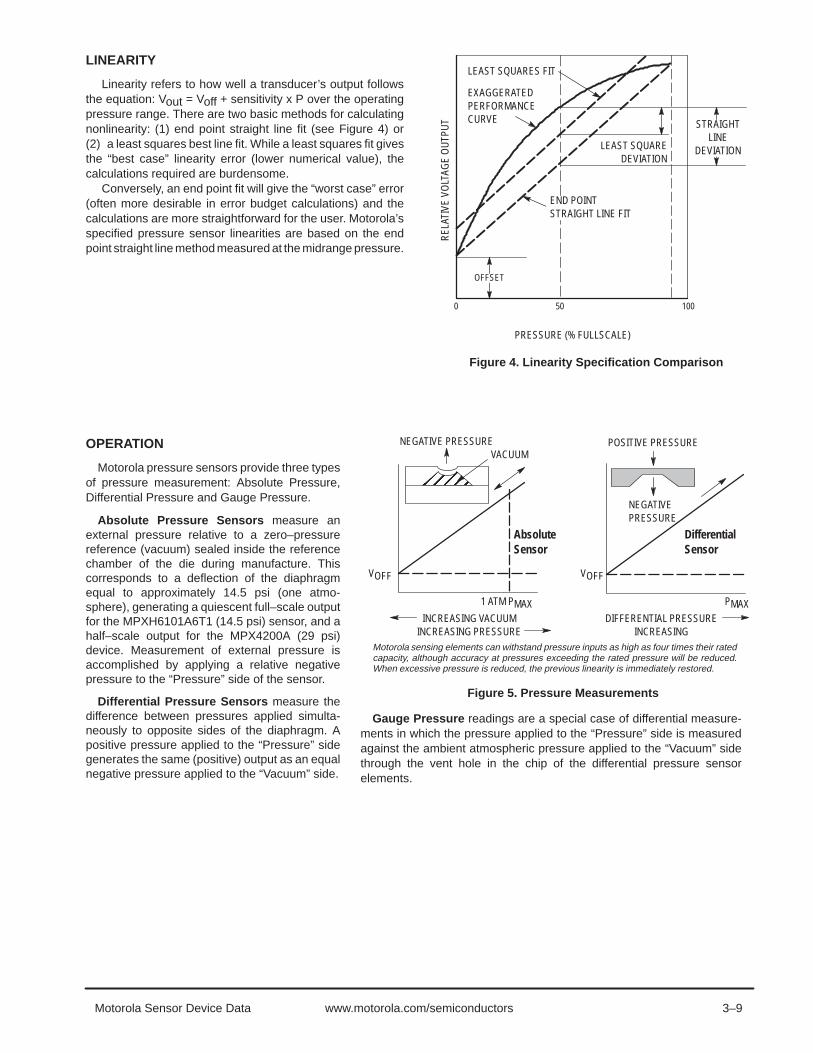
Figure 4. Linearity Specification Comparison
REL
ATIV
E VO
LTAG
E O
UTP
UT
LEAST SQUAREDEVIATION
0 50 100
PRESSURE (% FULLSCALE)
STRAIGHTLINE
DEVIATION
LEAST SQUARES FIT
EXAGGERATEDPERFORMANCECURVE
OFFSET
END POINTSTRAIGHT LINE FIT
3–9Motorola Sensor Device Data www.motorola.com/semiconductors
LINEARITY
Linearity refers to how well a transducer’s output followsthe equation: Vout = Voff + sensitivity x P over the operatingpressure range. There are two basic methods for calculatingnonlinearity: (1) end point straight line fit (see Figure 4) or(2) a least squares best line fit. While a least squares fit givesthe “best case” linearity error (lower numerical value), thecalculations required are burdensome.
Conversely, an end point fit will give the “worst case” error(often more desirable in error budget calculations) and thecalculations are more straightforward for the user. Motorola’sspecified pressure sensor linearities are based on the endpoint straight line method measured at the midrange pressure.
OPERATION
Motorola pressure sensors provide three typesof pressure measurement: Absolute Pressure,Differential Pressure and Gauge Pressure.
Absolute Pressure Sensors measure anexternal pressure relative to a zero–pressurereference (vacuum) sealed inside the referencechamber of the die during manufacture. Thiscorresponds to a deflection of the diaphragmequal to approximately 14.5 psi (one atmo-sphere), generating a quiescent full–scale outputfor the MPXH6101A6T1 (14.5 psi) sensor, and ahalf–scale output for the MPX4200A (29 psi)device. Measurement of external pressure isaccomplished by applying a relative negativepressure to the “Pressure” side of the sensor.
Differential Pressure Sensors measure thedifference between pressures applied simulta-neously to opposite sides of the diaphragm. Apositive pressure applied to the “Pressure” sidegenerates the same (positive) output as an equalnegative pressure applied to the “Vacuum” side.
Figure 5. Pressure Measurements
Gauge Pressure readings are a special case of differential measure-ments in which the pressure applied to the “Pressure” side is measuredagainst the ambient atmospheric pressure applied to the “Vacuum” sidethrough the vent hole in the chip of the differential pressure sensorelements.
ÉÉÉÉ
NEGATIVE PRESSURE
VOFF
1 ATM PMAXINCREASING VACUUM
INCREASING PRESSURE
POSITIVE PRESSURE
NEGATIVEPRESSURE
VOFF
DIFFERENTIAL PRESSUREINCREASING
PMAX
AbsoluteSensor
DifferentialSensor
VACUUM
Motorola sensing elements can withstand pressure inputs as high as four times their ratedcapacity, although accuracy at pressures exceeding the rated pressure will be reduced.When excessive pressure is reduced, the previous linearity is immediately restored.

3–10 Motorola Sensor Device Datawww.motorola.com/semiconductors
OU
TPU
T (m
Vdc)
kPaPSI
40
35
30
25
15
10
5
0
– 50 25
3.6250
7.2575
10.8710014.5
SPANRANGE(TYP)
OFFSET(TYP)
TYP
20
PRESSURE DIFFERENTIAL
OU
TPU
T (m
Vdc)
100
9080
70
60
5040
30
20
100
PSIkPa
0 1 2 3 4 5 6 7 80 10 20 30 40 50
– 40°C
Typical Electrical Characteristic Curves
VS = 10 VdcTA = 25°CMPX2100P1 > P2
MAX
MIN
+ 125°C
TA = – 40 TO + 125°CCOMPENSATED
COMPENSATED VS = 10 VdcUNCOMPENSATED VS = 3 VdcP1 > P2
UNCOMPENSATED
Figure 6. Output versus Pressure Differential Figure 7. Typical–Output Voltage versusPressure and Temperature for Compensated
and Uncompensated Devices
Figure 8. Signal Conditioned MPX5100
+ 25°C
0.5
0
1.0
TYP
MIN
4.55.0
4.0
3.5
3.0
2.5
2.0
1.5
0 10 50 70 11020 30 40 60 80 90 100
MAX
OU
TPU
T (V
olts
)
DIFFERENTIAL PRESSURE (in kPa)
TRANSFER FUNCTION:Vout = Vs* (0.009*P – 0.04) ± errorVs = 5.0 VdcTEMP = 0 to 85°CMPX5100DP1 > P2

3–11Motorola Sensor Device Data www.motorola.com/semiconductors
Unibody Cross–sectional Drawings
Figure 9. Cross–Sectional Diagrams (not to scale)
ÉÉÉÉÉÉÉÉÉÉÉÉÉÉÉÉÉÉÉÉÉÉÉÉÉÉÉÉÉÉÉÉÉÉÉÉÉÉÉÉÉÉÉÉÉÉÉÉÉÉÉÉÉÉÉ
SILICONE GELDIE COAT
WIRE BOND
LEAD FRAME
DIFFERENTIAL/GAUGEDIE STAINLESS STEEL
METAL COVER
EPOXYCASE
DIFFERENTIAL/GAUGE ELEMENT
DIEBOND
ÉÉÉÉÉÉÉÉÉÉÉÉÉÉÉÉÉÉÉÉÉÉÉÉÉÉÉÉÉÉÉÉÉÉÉÉÉÉÉÉÉÉÉÉÉÉÉÉÉÉÉÉÉÉÉ
SILICONE GELDIE COAT
WIRE BOND
LEAD FRAME
ABSOLUTEDIE
STAINLESS STEELMETAL COVER
EPOXYCASE
DIEBONDABSOLUTE ELEMENT
P1
P2
P1
Figure 9 illustrates the absolute sensing configuration(right) and the differential or gauge configuration in the basicchip carrier (Case 344). A silicone gel isolates the die surfaceand wire bonds from harsh environments, while allowing thepressure signal to be transmitted to the silicon diaphragm.
The MPX series pressure sensor operating characteristicsand internal reliability and qualification tests are based on useof dry air as the pressure media. Media other than dry air mayhave adverse effects on sensor performance and long termstability. Contact the factory for information regarding mediacompatibility in your application.
Figure 10. Cross–Sectional Diagram (not to scale)
FLUORO SILICONEDIE COAT
WIRE BONDS
LEAD FRAME
DIE
STAINLESS STEELMETAL COVER
EPOXY CASE
P1
Figure 10 illustrates the differential/gauge die in thebasic chip carrier (Case 473). A silicone gel isolates thedie surface and wirebonds from the environment, while
allowing the pressure signal to be transmitted to thesilicon diaphragm.

3–12 Motorola Sensor Device Datawww.motorola.com/semiconductors
IntegrationON-CHIP SIGNAL CONDITIONING
To make the designer’s job even easier, Motorola’sintegrated devices carry sensor technology one step further.In addition to the on-chip temperature compensation andcalibration offered currently on the 2000 series, amplifiersignal conditioning has been integrated on-chip in the 4000,5000 and 6000 series to allow interface directly to anymicrocomputer with an on-board A/D converter.
The signal conditioning is accomplished by means of afour-stage amplification network, incorporating linear bipolarprocessing, thin-film metallization techniques, and interac-tive laser trimming to provide the state-of-the-art in sensortechnology.
1.0 F
IPS
OUTPUT3
5 V
0.01 F
2
1
Recommended Power Supply Decoupling.For output filtering recommendations, please refer
to Application Note AN1646.
470 pF
Design Considerations for Different Levels of Sensor Integration
DESIGN ADVANTAGES DESIGN CONSIDERATIONS
Uncompensated Sensors High Sensitivity Device–to–Device Variation in Offsetand Span
Lowest Device Cost Temperature CompensationCircuitry Required
Low–Level Output Allows Flexibilityof Signal Conditioning
Requires Signal Conditioning/Amplification of Output Signal
Relatively Low Input Impedance(400 Ω Typical)
Temperature Compensated &Calibrated (2000 Series)
Reduced Device–to–DeviceVariations in Offset and Span
Lower Sensitivity Due to SpanCompensation (Compared toUncompensated)
Reduced Temperature Drift in Offsetand Span
Priced Higher than UncompensatedDevice
Reasonable Input Impedance(2K Ω Typical)
Requires Signal Conditioning/Amplification of Output Signal
Low Level Output Allows Flexibility inSignal Conditioning
Integrated Pressure Sensors(4000, 5000 and 6000 Series)
No Amplification NeededDirect Interface to MPU
Priced Higher than Compensated/Uncompensated Device
Signal Conditioning, Calibration ofSpan and Offset, TemperatureCompensation Included On–Chip

3–13Motorola Sensor Device Data www.motorola.com/semiconductors
Sensor ApplicationsAUTOMOTIVE/AVIATION APPLICATIONS
• Fuel Level Indicator
• Altimeters
• Air Speed Indicator
• Ejection Seat Control
• Turbo Boost Control
• Manifold Vacuum Control
• Fuel Flow Metering
• Oil Filter Flow Indicator
• Oil Pressure Sensor
• Air Flow Measurement
• Anti–Start
• Breathalizer Systems
• Smart Suspension Systems
• Variometer–Hang glider & Sailplanes
• Automotive Speed Control
HEALTHCARE APPLICATIONS
• Blood Pressure
• Esophagus Pressure
• Heart Monitor
• Interoccular Pressure
• Saline Pumps
• Kidney Dialysis
• Blood Gas Analysis
• Blood Serum Analysis
• Seating Pressure (Paraplegic)
• Respiratory Control
• Intravenous Infusion Pump Control
• Hospital Beds
• Drug Delivery
• IUPC
• Patient Monitors
INDUSTRIAL/COMMERCIAL APPLICATIONS
• Electronic Fire Fighting Control
• Flow Control
• Barometer
• HVAC Systems
• Tire Pressure Monitoring
• Water Filtered Systems (Flow Rate Indicator)
• Air Filtered Systems (Flow Rate Indicator)
• Tactile Sensing for Robotic Systems
• Boiler Pressure Indicators
• End of Tape Readers
• Disc Drive Control/Protection Systems
• Ocean Wave Measurement
• Diving Regulators
• Oil Well Logging
• Building Automation (Balancing, Load Control, Windows)
• Fluid Dispensers
• Explosion Sensing — Shock Wave Monitors
• Load Cells
• Autoclave Release Control
• Soil Compaction Monitor — Construction
• Water Depth Finders (Industrial, Sport Fishing/Diving)
• Pneumatic Controls — Robotics
• Pinch Roller Pressure — Paper Feed
• Blower Failure Safety Switch — Computer
• Vacuum Cleaner Control
• Electronic Drum
• Pressure Controls Systems — Building, Domes
• Engine Dynamometer
• Water Level Monitoring
• Altimeters
Motorola has tested media tolerant sensor devices in selected solutions or environments and test results are based on particular conditions andprocedures selected by Motorola. Customers are advised that the results may vary for actual services conditions. Customers are cautioned thatthey are responsible to determine the media compatibility of sensor devices in their applications and the foreseeable use and misuses of theirapplications.

3–14 Motorola Sensor Device Datawww.motorola.com/semiconductors
Pressure Sensor FAQ’sWe have discovered that many of our customers have
similar questions about certain aspects of our pressuresensor technology and operation. Here are the mostfrequently asked questions and answers that have beenexplained in relatively non–technical terms.
Q. How do I calculate total pressure error for myapplications?
A. You can calculate total error in two fashions, worst caseerror and most probable error. Worst case error is takingall the individual errors and adding them up, while mostprobable error sums the squares of the individual errorsand then take the square root of the total. In summary,Error (Worst Case) = E1 + E2 + E3 + ... + En, while Error(Most Probable) = SQRT[(E1)2 + (E2)2 + (E3)2 + ...(En)2]; Please note that not all errors may apply in yourindividual application.
Q. What is the media tolerance of our pressure sen-sors?
A. Most Motorola pressure sensors are specifically de-signed for dry air applications. However, Motorola nowoffers an MPXAZ series specifically designed for im-proved media resistance. This series incorporates adurable barrier that allows the sensor to operate reliablyin high humidity conditions as well as environmentscontaining common automotive media. NOTE: Applica-tions exposing the sensor to media other than what hasbeen specified could potentially limit the lifetime of thesensor. Please consult the Motorola factory for moreinformation regarding media compatibility in your specificapplication.
Q. Can I pull a vacuum on P1?
A. Motorola pressure sensors are designed to measurepressure in one direction and are not bi–directional. It is
possible to measure either a positive pressure OR anegative pressure, but not both. For example, the sensorcan be designed to accept a ”positive” pressure on theP1 port, providing that P1 is greater or equal to P2 whilestaying with in the sensors specified pressure range. Or,the sensor can measure ”negative” pressure (a vacu-um)by applying the pressure to the P2 port, again whileP1 is greater or equal to P2 and staying within thesensors specified range.
Our pressure sensors are based on a silicon diaphragmand can not tolerate a pressure that alternates frompositive to negative without resulting damage. Thedevices are rated for over pressure and burst but shouldnot be intentionally designed to operate in a bi–direction-al manner.
If you need to measure both a positive and negativepressure within the same system, we suggest designingwith two separate sensors, one for each pressure type.Or, a mechanical pressure transducer should be utilized.
Q. What will happen if I run the pressure sensor beyondthe rated operating pressure?
A. For bare elements (uncompensated and compensatedseries devices), when you take the sensor higher thanthe rated pressure, the part will still provide an outputincreasing linearly with pressure. When you go below theminimum rated pressure, the output of the sensor willeventually go negative. Motorola, however, does notguarantee electrical specifications beyond the ratedoperating pressure range specified in the data sheet ofeach device. The integrated series devices will notfunction at all beyond the rated pressure of the part.These series of parts will saturate at near 4.8 V and 0.2 Vand thus no further change in output will occur.

3–15Motorola Sensor Device Data www.motorola.com/semiconductors
!
The MPX10 and MPXV10GC series devices are silicon piezoresistive pressure sensorsproviding a very accurate and linear voltage output — directly proportional to the appliedpressure. These standard, low cost, uncompensated sensors permit manufacturers todesign and add their own external temperature compensation and signal conditioningnetworks. Compensation techniques are simplified because of the predictability ofMotorola’s single element strain gauge design. Figure 1 shows a schematic of the internalcircuitry on the stand–alone pressure sensor chip.
Features
• Low Cost
• Patented Silicon Shear Stress Strain Gauge Design
• Ratiometric to Supply Voltage
• Easy to Use Chip Carrier Package Options
• Differential and Gauge Options
• Durable Epoxy Unibody Element or Thermoplastic(PPS) Surface Mount Package
Application Examples
• Air Movement Control
• Environmental Control Systems
• Level Indicators
• Leak Detection
• Medical Instrumentation
• Industrial Controls
• Pneumatic Control Systems
• Robotics
Figure 1. Uncompensated PressureSensor Schematic
3
SENSINGELEMENT
2
4
+ Vout
– Vout
+ VS
1 GND
VOLTAGE OUTPUT versus APPLIED DIFFERENTIAL PRESSURE
The output voltage of the differential or gauge sensor increases with increasing pressureapplied to the pressure side (P1) relative to the vacuum side (P2). Similarly, output voltageincreases as increasing vacuum is applied to the vacuum side (P2) relative to the pressureside (P1).
SEMICONDUCTOR TECHNICAL DATA
0 to 10 kPa (0–1.45 psi)35 mV FULL SCALE SPAN
(TYPICAL)
NOTE: Pin 1 is noted by the notch inthe lead.
PIN NUMBER
MPX10DCASE 344
MPX10DPCASE 344C
1
2
Gnd
+Vout
3
4
VS
–Vout
UNIBODY PACKAGESMALL OUTLINE PACKAGE
MPXV10GC6UCASE 482A
MPXV10GC7UCASE 482C
PIN NUMBER
1
2
3
Gnd
+VoutVs
5
6
7
N/C
N/C
N/C
4 –Vout 8 N/C
NOTE: Pin 1 is noted by the notch inthe lead.
REV 10

3–16 Motorola Sensor Device Datawww.motorola.com/semiconductors
MAXIMUM RATINGS(NOTE)
Rating Symbol Value Unit
Maximum Pressure (P1 > P2) Pmax 75 kPa
Burst Pressure (P1 > P2) Pburst 100 kPa
Storage Temperature Tstg –40 to +125 °C
Operating Temperature TA –40 to +125 °C
NOTE: Exposure beyond the specified limits may cause permanent damage or degradation to the device.
OPERATING CHARACTERISTICS (VS = 3.0 Vdc, TA = 25°C unless otherwise noted, P1 > P2)
Characteristic Symbol Min Typ Max Unit
Differential Pressure Range(1) POP 0 — 10 kPa
Supply Voltage(2) VS — 3.0 6.0 Vdc
Supply Current Io — 6.0 — mAdc
Full Scale Span(3) VFSS 20 35 50 mV
Offset(4) Voff 0 20 35 mV
Sensitivity ∆V/∆P — 3.5 — mV/kPa
Linearity(5) — –1.0 — 1.0 %VFSS
Pressure Hysteresis(5) (0 to 10 kPa) — — ± 0.1 — %VFSS
Temperature Hysteresis(5) (–40°C to +125°C) — — ± 0.5 — %VFSS
Temperature Coefficient of Full Scale Span(5) TCVFSS –0.22 — –0.16 %VFSS/°C
Temperature Coefficient of Offset(5) TCVoff — ±15 — µV/°C
Temperature Coefficient of Resistance(5) TCR 0.28 — 0.34 %Zin/°C
Input Impedance Zin 400 — 550 Ω
Output Impedance Zout 750 — 1250 Ω
Response Time(6) (10% to 90%) tR — 1.0 — ms
Warm–Up Time(7) — — 20 — ms
Offset Stability(8) — — ±0.5 — %VFSSNOTES:
1. 1.0 kPa (kiloPascal) equals 0.145 psi.2. Device is ratiometric within this specified excitation range. Operating the device above the specified excitation range may induce additional
error due to device self–heating.3. Full Scale Span (VFSS) is defined as the algebraic difference between the output voltage at full rated pressure and the output voltage at the
minimum rated pressure.4. Offset (Voff) is defined as the output voltage at the minimum rated pressure.5. Accuracy (error budget) consists of the following:
• Linearity: Output deviation from a straight line relationship with pressure, using end point method, over the specified pressure range.
• Temperature Hysteresis: Output deviation at any temperature within the operating temperature range, after the temperature is cycled to and from the minimum or maximum operating temperature points, with zero differential pressure applied.
• Pressure Hysteresis: Output deviation at any pressure within the specified range, when this pressure is cycled to and from the minimum or maximum rated pressure, at 25°C.
• TcSpan: Output deviation at full rated pressure over the temperature range of 0 to 85°C, relative to 25°C.• TcOffset: Output deviation with minimum rated pressure applied, over the temperature range of 0 to 85°C, relative
to 25°C.• TCR: Zin deviation with minimum rated pressure applied, over the temperature range of –40°C to +125°C,
relative to 25°C.6. Response Time is defined as the time for the incremental change in the output to go from 10% to 90% of its final value when subjected to
a specified step change in pressure.7. Warm–up Time is defined as the time required for the product to meet the specified output voltage after the pressure has been stabilized.8. Offset Stability is the product’s output deviation when subjected to 1000 hours of Pulsed Pressure, Temperature Cycling with Bias Test.

3–17Motorola Sensor Device Data www.motorola.com/semiconductors
TEMPERATURE COMPENSATIONFigure 2 shows the typical output characteristics of the
MPX10 and MPXV10GC series over temperature.Because this strain gauge is an integral part of the silicon
diaphragm, there are no temperature effects due to differ-ences in the thermal expansion of the strain gauge and thediaphragm, as are often encountered in bonded strain gaugepressure sensors. However, the properties of the straingauge itself are temperature dependent, requiring that thedevice be temperature compensated if it is to be used overan extensive temperature range.
Temperature compensation and offset calibration can beachieved rather simply with additional resistive components,or by designing your system using the MPX2010D seriessensor.
Several approaches to external temperature compensa-
tion over both –40 to +125°C and 0 to +80°C ranges arepresented in Motorola Applications Note AN840.
LINEARITYLinearity refers to how well a transducer’s output follows
the equation: Vout = Voff + sensitivity x P over the operatingpressure range (Figure 3). There are two basic methods forcalculating nonlinearity: (1) end point straight line fit or (2) aleast squares best line fit. While a least squares fit gives the“best case” linearity error (lower numerical value), the cal-culations required are burdensome.
Conversely, an end point fit will give the “worst case” error(often more desirable in error budget calculations) and thecalculations are more straightforward for the user. Motorola’sspecified pressure sensor linearities are based on the endpoint straight line method measured at the midrange pressure.
Figure 2. Output versus Pressure Differential Figure 3. Linearity Specification Comparison
Figure 4. Unibody Package — Cross–SectionalDiagram (not to scale)
ÉÉÉÉÉÉÉÉÉÉÉÉÉÉÉÉÉÉÉÉÉÉÉÉÉÉÉÉÉÉÉÉÉÉÉÉÉÉÉÉÉÉÉÉÉÉÉÉÉÉÉÉÉÉÉ
SILICONEDIE COAT
WIRE BOND
LEAD FRAME
DIE STAINLESS STEELMETAL COVER
EPOXYCASE
RTV DIEBOND
P1
P2
OFFSET(VOFF)
70
OU
TPU
T (m
Vdc)
60
50
40
30
20
10
00 MAX POP
SPAN(VFSS)
PRESSURE (kPA)
ACTUAL
THEORETICAL
LINEARITY
PRESSURE DIFFERENTIAL
OU
TPU
T (m
Vdc)
80
70
60
50
40
30
20
10
00 0.3
2.0
0.6
4.0
0.9
6.0
1.2
8.0 10
1.5PSI
kPa
SPANRANGE(TYP)
OFFSET(TYP)
VS = 3 VdcP1 > P2
– 40°C+ 25°C
+ 125°C
Figure 4 illustrates the differential or gauge configurationin the basic chip carrier (Case 344). A silicone gel isolatesthe die surface and wire bonds from the environment, whileallowing the pressure signal to be transmitted to the silicondiaphragm.
The MPX10 and MPXV10GC series pressure sensor oper-
ating characteristics and internal reliability and qualificationtests are based on use of dry air as the pressure media. Me-dia other than dry air may have adverse effects on sensor per-formance and long term reliability. Contact the factory forinformation regarding media compatibility in your application.

3–18 Motorola Sensor Device Datawww.motorola.com/semiconductors
PRESSURE (P1)/VACUUM (P2) SIDE IDENTIFICATION TABLE
Motorola designates the two sides of the pressure sensoras the Pressure (P1) side and the Vacuum (P2) side. ThePressure (P1) side is the side containing silicone gel whichisolates the die from the environment. The Motorola pres-
sure sensor is designed to operate with positive differentialpressure applied, P1 > P2.
The Pressure (P1) side may be identified by using the tablebelow:
Part Number Case Type Pressure (P1) Side Identifier
MPX10D 344 Stainless Steel Cap
MPX10DP 344C Side with Part Marking
MPX10GP 344B Side with Port Attached
MPX10GS 344E Side with Port Attached
MPXV10GC6U 482A Side with Part Marking
MPXV10GC7U 482C Side with Part Marking
ORDERING INFORMATION — UNIBODY PACKAGE
MPX10 series pressure sensors are available in differential and gauge configurations. Devices are available in the basicelement package or with pressure port fittings which provide printed circuit board mounting ease and barbed hose pressureconnections.
MPX Series
Device Type Options Case Type Order Number Device Marking
Basic Element Differential Case 344 MPX10D MPX10D
Ported Elements Differential Case 344C MPX10DP MPX10DP
Gauge Case 344B MPX10GP MPX10GP
Gauge Case 344E MPX10GS MPX10D
ORDERING INFORMATION — SMALL OUTLINE PACKAGE (MPXV10GC SERIES)
Device Type/Order No Packing Options Case Type Device MarkingDevice Type/Order No. Packing Options Case Type Device Marking
MPXV10GC6U Rails Case 482A MPXV10G
MPXV10GC6T1 Tape and Reel Case 482A MPXV10G
MPXV10GC7U Rails Case 482C MPXV10G

3–19Motorola Sensor Device Data www.motorola.com/semiconductors
The MPX12 series device is a silicon piezoresistive pressure sensor providing a veryaccurate and linear voltage output — directly proportional to the applied pressure. Thisstandard, low cost, uncompensated sensor permits manufacturers to design and addtheir own external temperature compensating and signal conditioning networks.Compensation techniques are simplified because of the predictability of Motorola’s singleelement strain gauge design.
Features
• Low Cost
• Patented Silicon Shear Stress Strain Gauge Design
• Ratiometric to Supply Voltage
• Easy to Use Chip Carrier Package Options
• Differential and Gauge Options
• Durable Epoxy Package
Application Examples
• Air Movement Control
• Environmental Control Systems
• Level Indicators
• Leak Detection
• Medical Instrumentation
• Industrial Controls
• Pneumatic Control Systems
• Robotics
Figure 1 shows a schematic of the internal circuitry on the stand–alone pressuresensor chip.
Figure 1. Uncompensated Pressure Sensor Schematic
PIN 3
SENSINGELEMENT
PIN 2
PIN 4
+ Vout
– Vout
+ VS
PIN 1
VOLTAGE OUTPUT versus APPLIED DIFFERENTIAL PRESSURE
The output voltage of the differential or gauge sensor increases with increasingpressure applied to the pressure side (P1) relative to the vacuum side (P2). Similarly,output voltage increases as increasing vacuum is applied to the vacuum side (P2)relative to the pressure side (P1).
SEMICONDUCTOR TECHNICAL DATA
0 to 10 kPa (0–1.45 psi)55 mV FULL SCALE SPAN
(TYPICAL)
PIN NUMBER
MPX12DCASE 344
MPX12DPCASE 344C
1
2
Gnd
+Vout
3
4
VS
–Vout
NOTE: Pin 1 is noted by the notch inthe lead.
REV 3

3–20 Motorola Sensor Device Datawww.motorola.com/semiconductors
MAXIMUM RATINGS(NOTE)
Rating Symbol Value Unit
Maximum Pressure (P1 > P2) Pmax 75 kPa
Burst Pressure (P1 > P2) Pburst 100 kPa
Storage Temperature Tstg –40 to +125 °C
Operating Temperature TA –40 to +125 °C
NOTE: Exposure beyond the specified limits may cause permanent damage or degradation to the device.
OPERATING CHARACTERISTICS (VS = 3.0 Vdc, TA = 25°C unless otherwise noted, P1 > P2)
Characteristic Symbol Min Typ Max Unit
Differential Pressure Range(1) POP 0 — 10 kPa
Supply Voltage(2) VS — 3.0 6.0 Vdc
Supply Current Io — 6.0 — mAdc
Full Scale Span(3) VFSS 45 55 70 mV
Offset(4) Voff 0 20 35 mV
Sensitivity ∆V/∆P — 5.5 — mV/kPa
Linearity(5) — –0.5 — 5.0 %VFSS
Pressure Hysteresis(5) (0 to 10 kPa) — — ± 0.1 — %VFSS
Temperature Hysteresis(5) (–40°C to +125°C) — — ± 0.5 — %VFSS
Temperature Coefficient of Full Scale Span(5) TCVFSS –0.22 — –0.16 %VFSS/°C
Temperature Coefficient of Offset(5) TCVoff — ±15 — µV/°C
Temperature Coefficient of Resistance(5) TCR 0.28 — 0.34 %Zin/°C
Input Impedance Zin 400 — 550 Ω
Output Impedance Zout 750 — 1250 Ω
Response Time(6) (10% to 90%) tR — 1.0 — ms
Warm–Up Time(7) — — 20 — ms
Offset Stability(8) — — ±0.5 — %VFSSNOTES:
1. 1.0 kPa (kiloPascal) equals 0.145 psi.2. Device is ratiometric within this specified excitation range. Operating the device above the specified excitation range may induce additional
error due to device self–heating.3. Full Scale Span (VFSS) is defined as the algebraic difference between the output voltage at full rated pressure and the output voltage at the
minimum rated pressure.4. Offset (Voff) is defined as the output voltage at the minimum rated pressure.5. Accuracy (error budget) consists of the following:
• Linearity: Output deviation from a straight line relationship with pressure, using end point method, over the specified pressure range.
• Temperature Hysteresis: Output deviation at any temperature within the operating temperature range, after the temperature is cycled to and from the minimum or maximum operating temperature points, with zero differential pressure applied.
• Pressure Hysteresis: Output deviation at any pressure within the specified range, when this pressure is cycled to and from the minimum or maximum rated pressure, at 25°C.
• TcSpan: Output deviation at full rated pressure over the temperature range of 0 to 85°C, relative to 25°C.• TcOffset: Output deviation with minimum rated pressure applied, over the temperature range of 0 to 85°C, relative
to 25°C.• TCR: Zin deviation with minimum rated pressure applied, over the temperature range of –40°C to +125°C,
relative to 25°C.6. Response Time is defined as the time for the incremental change in the output to go from 10% to 90% of its final value when subjected to
a specified step change in pressure.7. Warm–up Time is defined as the time required for the product to meet the specified output voltage after the pressure has been stabilized.8. Offset Stability is the product’s output deviation when subjected to 1000 hours of Pulsed Pressure, Temperature Cycling with Bias Test.

3–21Motorola Sensor Device Data www.motorola.com/semiconductors
TEMPERATURE COMPENSATIONFigure 2 shows the typical output characteristics of the
MPX12 series over temperature.Because this strain gauge is an integral part of the silicon
diaphragm, there are no temperature effects due to differ-ences in the thermal expansion of the strain gauge and thediaphragm, as are often encountered in bonded strain gaugepressure sensors. However, the properties of the straingauge itself are temperature dependent, requiring that thedevice be temperature compensated if it is to be used overan extensive temperature range.
Temperature compensation and offset calibration can beachieved rather simply with additional resistive components,or by designing your system using the MPX2010D seriessensor.
Several approaches to external temperature compensa-
tion over both –40 to +125°C and 0 to +80°C ranges arepresented in Motorola Applications Note AN840.
LINEARITYLinearity refers to how well a transducer’s output follows
the equation: Vout = Voff + sensitivity x P over the operatingpressure range (Figure 3). There are two basic methods forcalculating nonlinearity: (1) end point straight line fit or (2) aleast squares best line fit. While a least squares fit gives the“best case” linearity error (lower numerical value), the cal-culations required are burdensome.
Conversely, an end point fit will give the “worst case” error(often more desirable in error budget calculations) and thecalculations are more straightforward for the user. Motoro-la’s specified pressure sensor linearities are based on theend point straight line method measured at the midrangepressure.
Figure 2. Output versus Pressure Differential Figure 3. Linearity Specification Comparison
Figure 4. Cross–Sectional Diagram (not to scale)
ÉÉÉÉÉÉÉÉÉÉÉÉÉÉÉÉÉÉÉÉÉÉÉÉÉÉÉÉÉÉÉÉÉÉÉÉÉÉÉÉÉÉÉÉÉÉÉÉÉÉÉÉÉÉÉ
SILICONEDIE COAT
WIRE BOND
LEAD FRAME
DIE STAINLESS STEELMETAL COVER
EPOXYCASE
RTV DIEBOND
P1
P2
OFFSET(VOFF)
70
OU
TPU
T (m
Vdc)
60
50
40
30
20
10
00 MAX POP
SPAN(VFSS)
PRESSURE (kPA)
ACTUAL
THEORETICAL
LINEARITY
PRESSURE DIFFERENTIAL
OU
TPU
T (m
Vdc)
80
70
60
50
40
30
20
10
00 0.3
2.0
0.6
4.0
0.9
6.0
1.2
8.0 10
1.5PSI
kPa
SPANRANGE(TYP)
OFFSET(TYP)
VS = 3 VdcP1 > P2
– 40°C+ 25°C
+ 125°C
Figure 4 illustrates the differential or gauge configurationin the basic chip carrier (Case 344). A silicone gel isolatesthe die surface and wire bonds from the environment, whileallowing the pressure signal to be transmitted to the silicondiaphragm.
The MPX12 series pressure sensor operating characteris-
tics and internal reliability and qualification tests are basedon use of dry air as the pressure media. Media other thandry air may have adverse effects on sensor performance andlong term reliability. Contact the factory for information re-garding media compatibility in your application.
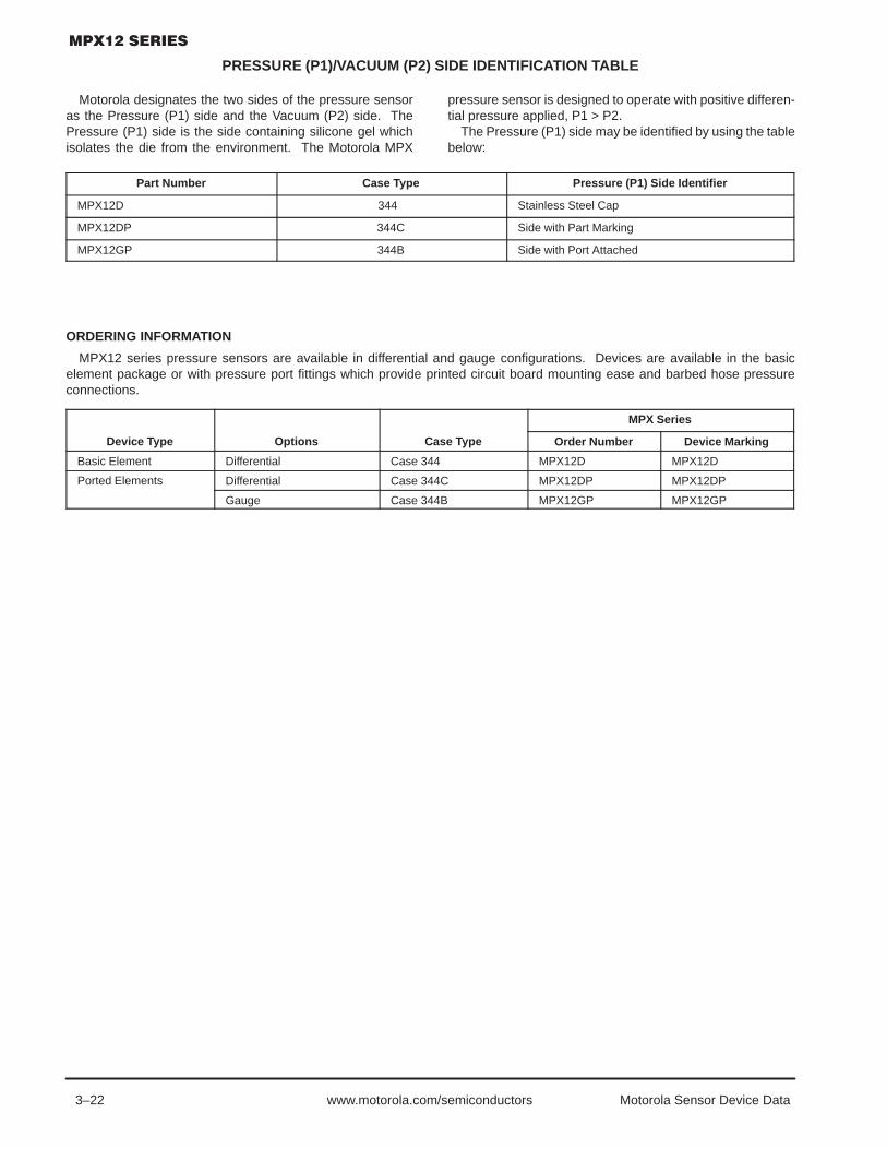
3–22 Motorola Sensor Device Datawww.motorola.com/semiconductors
PRESSURE (P1)/VACUUM (P2) SIDE IDENTIFICATION TABLE
Motorola designates the two sides of the pressure sensoras the Pressure (P1) side and the Vacuum (P2) side. ThePressure (P1) side is the side containing silicone gel whichisolates the die from the environment. The Motorola MPX
pressure sensor is designed to operate with positive differen-tial pressure applied, P1 > P2.
The Pressure (P1) side may be identified by using the tablebelow:
Part Number Case Type Pressure (P1) Side Identifier
MPX12D 344 Stainless Steel Cap
MPX12DP 344C Side with Part Marking
MPX12GP 344B Side with Port Attached
ORDERING INFORMATION
MPX12 series pressure sensors are available in differential and gauge configurations. Devices are available in the basicelement package or with pressure port fittings which provide printed circuit board mounting ease and barbed hose pressureconnections.
MPX Series
Device Type Options Case Type Order Number Device Marking
Basic Element Differential Case 344 MPX12D MPX12D
Ported Elements Differential Case 344C MPX12DP MPX12DP
Gauge Case 344B MPX12GP MPX12GP

3–23Motorola Sensor Device Data www.motorola.com/semiconductors
! !"$%" !#$ "$ "##%" # "#
The MPX2010 /MPXV2010G se r ies s i l i conpiezoresistive pressure sensors provide a veryaccurate and l inear vol tage output — direct lyproportional to the applied pressure. These sensorshouse a single monolithic silicon die with the straingauge and thin–film resistor network integrated oneach chip. The sensor is laser trimmed for precises pan , o f f s e t ca l i b ra t i on and t empe ra tu recompensation.
Features
• Temperature Compensated over 0°C to +85°C• Ratiometric to Supply Voltage
• Differential and Gauge Options
Application Examples
• Respiratory Diagnostics
• Air Movement Control
• Controllers
• Pressure Switching
Figure 1 shows a block diagram of the internalcircuitry on the stand–alone pressure sensor chip.
Figure 1. Temperature Compensated and CalibratedPressure Sensor Schematic
VS
3
SENSINGELEMENT
THIN FILMTEMPERATURECOMPENSATION
ANDCALIBRATION
CIRCUITRY
2
4
Vout+
Vout–
1
GND
VOLTAGE OUTPUT versus APPLIED DIFFERENTIAL PRESSURE
The output voltage of the differential or gauge sensorincreases with increasing pressure applied to thepressure side (P1) relative to the vacuum side (P2).Similarly, output voltage increases as increasing vacu-um is applied to the vacuum side (P2) relative to thepressure side (P1).
Preferred devices are Motorola recommended choices for future use andbest overall value.
SEMICONDUCTOR TECHNICAL DATA
SMALL OUTLINE PACKAGESURFACE MOUNT
UNIBODY PACKAGE
MPX2010GPCASE 344B
MPX2010GSXCASE 344F
PIN NUMBER
NOTE: Pin 1 is noted by the notch inthe lead.
1
2
3
Gnd
+VoutVS
5
6
7
N/C
N/C
N/C
4 –Vout 8 N/C
MPX2010DCASE 344
MPX2010DPCASE 344C
MPX2010GSCASE 344E
MPXV2010DPCASE 1351
MPXV2010GPCASE 1369
COMPENSATEDPRESSURE SENSOR
0 to 10 kPa (0 to 1.45 psi)FULL SCALE SPAN: 25 mV
Motorola Preferred Device
PIN NUMBER
1
2
Gnd
+Vout
3
4
VS
–Vout
NOTE: Pin 1 is noted by the notch inthe lead.REV 9

3–24 Motorola Sensor Device Datawww.motorola.com/semiconductors
MAXIMUM RATINGS(NOTE)
Rating Symbol Value Unit
Maximum Pressure (P1 > P2) Pmax 75 kPa
Storage Temperature Tstg –40 to +125 °C
Operating Temperature TA –40 to +125 °C
NOTE: Exposure beyond the specified limits may cause permanent damage or degradation to the device.
OPERATING CHARACTERISTICS (VS = 10 Vdc, TA = 25°C unless otherwise noted, P1 > P2)
Characteristic Symbol Min Typ Max Unit
Pressure Range(1) POP 0 — 10 kPa
Supply Voltage(2) VS — 10 16 Vdc
Supply Current Io — 6.0 — mAdc
Full Scale Span(3) VFSS 24 25 26 mV
Offset(4) Voff –1.0 — 1.0 mV
Sensitivity ∆V/∆P — 2.5 — mV/kPa
Linearity(5) — –1.0 — 1.0 %VFSS
Pressure Hysteresis(5) (0 to 10 kPa) — — ±0.1 — %VFSS
Temperature Hysteresis(5) (–40°C to +125°C) — — ±0.5 — %VFSS
Temperature Effect on Full Scale Span(5) TCVFSS –1.0 — 1.0 %VFSS
Temperature Effect on Offset(5) TCVoff –1.0 — 1.0 mV
Input Impedance Zin 1000 — 2550 Ω
Output Impedance Zout 1400 — 3000 Ω
Response Time(6) (10% to 90%) tR — 1.0 — ms
Warm–Up — — 20 — ms
Offset Stability(7) — — ±0.5 — %VFSS
NOTES:1. 1.0 kPa (kiloPascal) equals 0.145 psi.2. Device is ratiometric within this specified excitation range. Operating the device above the specified excitation range may induce additional
error due to device self–heating.3. Full Scale Span (VFSS) is defined as the algebraic difference between the output voltage at full rated pressure and the output voltage at the
minimum rated pressure.4. Offset (Voff) is defined as the output voltage at the minimum rated pressure.5. Accuracy (error budget) consists of the following:
• Linearity: Output deviation from a straight line relationship with pressure, using end point method, over the specified pressure range.
• Temperature Hysteresis: Output deviation at any temperature within the operating temperature range, after the temperature is cycled to and from the minimum or maximum operating temperature points, with zero differential pressure applied.
• Pressure Hysteresis: Output deviation at any pressure within the specified range, when this pressure is cycled to and from the minimum or maximum rated pressure, at 25°C.
• TcSpan: Output deviation at full rated pressure over the temperature range of 0 to 85°C, relative to 25°C.• TcOffset: Output deviation with minimum rated pressure applied, over the temperature range of 0 to 85°C, relative
to 25°C.6. Response Time is defined as the time for the incremental change in the output to go from 10% to 90% of its final value when subjected to
a specified step change in pressure.7. Offset stability is the product’s output deviation when subjected to 1000 hours of Pulsed Pressure, Temperature Cycling with Bias Test.

3–25Motorola Sensor Device Data www.motorola.com/semiconductors
ON–CHIP TEMPERATURE COMPENSATION and CALIBRATION
Figure 2. Output versus Pressure Differential
MIN
TYP
OFFSET(TYP)
30
20
15
10
5
OU
TPU
T (m
Vdc)
25
0
– 5kPaPSI
2.50.362
50.725
7.51.09
101.45
aMAX SPANRANGE(TYP)
VS = 10 VdcTA = 25°CP1 > P2
Figure 2 shows the output character ist ics of theMPX2010/MPXV2010G series at 25°C. The output is direct-ly proportional to the differential pressure and is essentially astraight line.
The effects of temperature on full scale span and offset arevery small and are shown under Operating Characteristics.
This performance over temperature is achieved by havingboth the shear stress strain gauge and the thin–film resistorcircuitry on the same silicon diaphragm. Each chip is dynam-ically laser trimmed for precise span and offset calibrationand temperature compensation.
Figure 3. Unibody Package — Cross–SectionalDiagram (not to scale)
ÉÉÉÉÉÉÉÉÉÉÉÉÉÉÉÉÉÉÉÉÉÉÉÉÉÉÉÉÉÉÉÉÉÉÉÉÉÉÉÉÉÉÉÉÉÉÉÉÉÉÉÉÉÉÉ
SILICONEDIE COAT
WIRE BOND
LEAD FRAME
DIE
STAINLESS STEELMETAL COVER
EPOXYCASE
RTV DIEBOND
P1
P2
Figure 3 illustrates the differential/gauge die in the basicchip carrier (Case 344). A silicone gel isolates the die surfaceand wire bonds from the environment, while allowing the pres-sure signal to be transmitted to the silicon diaphragm.
The MPX2010/MPXV2010G series pressure sensor oper-
ating characteristics and internal reliability and qualificationtests are based on use of dry air as the pressure media. Me-dia other than dry air may have adverse effects on sensorperformance and long term reliability. Contact the factory forinformation regarding media compatibility in your application.

3–26 Motorola Sensor Device Datawww.motorola.com/semiconductors
LINEARITYLinearity refers to how well a transducer’s output follows
the equation: Vout = Voff + sensitivity x P over the operatingpressure range. There are two basic methods for calculatingnonlinearity: (1) end point straight line fit (see Figure 5) or (2)a least squares best line fit. While a least squares fit givesthe “best case” linearity error (lower numerical value), thecalculations required are burdensome.
Conversely, an end point fit will give the “worst case” error(often more desirable in error budget calculations) and the cal-culations are more straightforward for the user. Motorola’sspecified pressure sensor linearities are based on the endpoint straight line method measured at the midrange pressure.
Figure 4. Linearity Specification Comparison
LEASTSQUAREDEVIATION
REL
ATIV
E VO
LTAG
E O
UTP
UT
PRESSURE (% FULLSCALE)0 50 100
END POINTSTRAIGHT LINE FIT
EXAGGERATED PERFORMANCECURVE
LEAST SQUARES FIT
STRAIGHT LINEDEVIATION
OFFSET
PRESSURE (P1)/VACUUM (P2) SIDE IDENTIFICATION TABLE
Motorola designates the two sides of the pressure sensoras the Pressure (P1) side and the Vacuum (P2) side. ThePressure (P1) side is the side containing silicone gel whichisolates the die from the environment. The Motorola MPX
pressure sensor is designed to operate with positive differen-tial pressure applied, P1 > P2.
The Pressure (P1) side may be identified by using thetable below:
Part Number Case Type Pressure (P1) Side Identifier
MPX2010D 344 Stainless Steel Cap
MPX2010DP 344C Side with Part Marking
MPX2010GP 344B Side with Port Attached
MPX2010GS 344E Side with Port Attached
MPX2010GSX 344F Side with Port Attached
MPXV2010GP 1369 Side with Port Attached
MPXV2010DP 1351 Side with Part Marking
ORDERING INFORMATION — UNIBODY PACKAGE (MPX2010 SERIES)
MPX Series
Device Type Options Case Type Order Number Device Marking
Basic Element Differential 344 MPX2010D MPX2010D
Ported Elements Differential, Dual Port 344C MPX2010DP MPX2010DP
Gauge 344B MPX2010GP MPX2010GP
Gauge, Axial 344E MPX2010GS MPX2010D
Gauge, Axial PC Mount 344F MPX2010GSX MPX2010D
ORDERING INFORMATION — SMALL OUTLINE PACKAGE (MPXV2010G SERIES)
Device Type Options Case No. MPX Series Order No. Packing Options Marking
Ported Elements Gauge, Side Port, SMT 1369 MPXV2010GP Trays MPXV2010G
Differential, Dual Port, SMT 1351 MPXV2010DP Trays MPXV2010G

3–27Motorola Sensor Device Data www.motorola.com/semiconductors
"# !" " !!# ! !
The MPX2050 series device is a silicon piezoresistive pressure sensors providing ahighly accurate and linear voltage output — directly proportional to the applied pressure.The sensor is a single, monolithic silicon diaphragm with the strain gauge and a thin–filmresistor network integrated on–chip. The chip is laser trimmed for precise span and offsetcalibration and temperature compensation.
Features
• Temperature Compensated Over 0°C to +85°C• Unique Silicon Shear Stress Strain Gauge
• Easy to Use Chip Carrier Package Options
• Ratiometric to Supply Voltage
• Differential and Gauge Options
• ± 0.25% Linearity (MPX2050)
Application Examples
• Pump/Motor Controllers
• Robotics
• Level Indicators
• Medical Diagnostics
• Pressure Switching
• Non–Invasive Blood Pressure Measurement
Figure 1 shows a block diagram of the internal circuitry on the stand–alone pressuresensor chip.
Figure 1. Temperature Compensated Pressure Sensor Schematic
VS
3
SENSINGELEMENT
THIN FILMTEMPERATURECOMPENSATION
ANDCALIBRATION
CIRCUITRY
2
4
Vout+
Vout–
1
GND
VOLTAGE OUTPUT versus APPLIED DIFFERENTIAL PRESSUREThe differential voltage output of the sensor is directly proportional to the differential
pressure applied.The output voltage of the differential or gauge sensor increases with increasing
pressure applied to the pressure side (P1) relative to the vacuum side (P2). Similarly,output voltage increases as increasing vacuum is applied to the vacuum side (P2)relative to the pressure side (P1).
SEMICONDUCTOR TECHNICAL DATA
0 to 50 kPa (0 to 7.25 psi)40 mV FULL SCALE SPAN
(TYPICAL)
PIN NUMBER
1
2
Gnd
+Vout
3
4
VS
–Vout
NOTE: Pin 1 is noted by the notch inthe lead.
MPX2050GPCASE 344B
MPX2050GSXCASE 344F
MPX2050DCASE 344
MPX2050DPCASE 344C
REV 8

3–28 Motorola Sensor Device Datawww.motorola.com/semiconductors
MAXIMUM RATINGS(NOTE)
Rating Symbol Value Unit
Maximum Pressure (P1 > P2) Pmax 200 kPa
Storage Temperature Tstg –40 to +125 °C
Operating Temperature TA –40 to +125 °C
NOTE: Exposure beyond the specified limits may cause permanent damage or degradation to the device.
OPERATING CHARACTERISTICS (VS = 10 Vdc, TA = 25°C unless otherwise noted, P1 > P2)
Characteristic Symbol Min Typ Max Unit
Pressure Range(1) POP 0 — 50 kPa
Supply Voltage(2) VS — 10 16 Vdc
Supply Current Io — 6.0 — mAdc
Full Scale Span(3) MPX2050 VFSS 38.5 40 41.5 mV
Offset(4) MPX2050 Voff –1.0 — 1.0 mV
Sensitivity ∆V/∆P — 0.8 — mV/kPa
Linearity(5) MPX2050 — –0.25 — 0.25 %VFSS
Pressure Hysteresis(5) (0 to 50 kPa) — — ±0.1 — %VFSS
Temperature Hysteresis(5) (–40°C to +125°C) — — ±0.5 — %VFSS
Temperature Effect on Full Scale Span(5) TCVFSS –1.0 — 1.0 %VFSS
Temperature Effect on Offset(5) TCVoff –1.0 — 1.0 mV
Input Impedance Zin 1000 — 2500 Ω
Output Impedance Zout 1400 — 3000 Ω
Response Time(6) (10% to 90%) tR — 1.0 — ms
Warm–Up — — 20 — ms
Offset Stability(7) — — ±0.5 — %VFSS
NOTES:1. 1.0 kPa (kiloPascal) equals 0.145 psi.2. Device is ratiometric within this specified excitation range. Operating the device above the specified excitation range may induce additional
error due to device self–heating.3. Full Scale Span (VFSS) is defined as the algebraic difference between the output voltage at full rated pressure and the output voltage at the
minimum rated pressure.4. Offset (Voff) is defined as the output voltage at the minimum rated pressure.5. Accuracy (error budget) consists of the following:
• Linearity: Output deviation from a straight line relationship with pressure, using end point method, over the specified pressure range.
• Temperature Hysteresis: Output deviation at any temperature within the operating temperature range, after the temperature is cycled to and from the minimum or maximum operating temperature points, with zero differential pressure applied.
• Pressure Hysteresis: Output deviation at any pressure within the specified range, when this pressure is cycled to and from the minimum or maximum rated pressure, at 25°C.
• TcSpan: Output deviation at full rated pressure over the temperature range of 0 to 85°C, relative to 25°C.• TcOffset: Output deviation with minimum rated pressure applied, over the temperature range of 0 to 85°C, relative
to 25°C.6. Response Time is defined as the time for the incremental change in the output to go from 10% to 90% of its final value when subjected to
a specified step change in pressure.7. Offset stability is the product’s output deviation when subjected to 1000 hours of Pulsed Pressure, Temperature Cycling with Bias Test.

3–29Motorola Sensor Device Data www.motorola.com/semiconductors
LINEARITYLinearity refers to how well a transducer’s output follows
the equation: Vout = Voff + sensitivity x P over the operatingpressure range. There are two basic methods for calculatingnonlinearity: (1) end point straight line fit (see Figure 2) or (2)a least squares best line fit. While a least squares fit givesthe “best case” linearity error (lower numerical value), thecalculations required are burdensome.
Conversely, an end point fit will give the “worst case” error(often more desirable in error budget calculations) and thecalculations are more straightforward for the user. Motorola’sspecified pressure sensor linearities are based on the endpoint straight line method measured at the midrange pres-sure.
Figure 2. Linearity Specification Comparison
LEASTSQUARE
DEVIATION
REL
ATIV
E VO
LTAG
E O
UTP
UT
PRESSURE (% FULLSCALE)0 50 100
END POINTSTRAIGHT LINE FIT
EXAGGERATED PERFORMANCECURVE
LEAST SQUARES FIT
STRAIGHT LINEDEVIATION
OFFSET
ON–CHIP TEMPERATURE COMPENSATION and CALIBRATION
Figure 3 shows the minimum, maximum and typical outputcharacteristics of the MPX2050 series at 25°C. The output isdirectly proportional to the differential pressure and is essen-tially a straight line.
The effects of temperature on Full–Scale Span and Offsetare very small and are shown under Operating Characteris-tics.
Figure 3. Output versus Pressure Differential Figure 4. Cross–Sectional Diagram (not to scale)
OU
TPU
T (m
Vdc)
kPaPSI
40
35
30
25
15
10
5
0– 5
0 12.51.8
253.6
37.55.4
507.25
SPANRANGE(TYP)
OFFSET(TYP)
20
ÉÉÉÉÉÉÉÉÉÉÉÉÉÉÉÉÉÉÉÉÉÉÉÉÉÉÉÉÉÉÉÉÉÉÉÉÉÉÉÉÉÉÉÉÉÉÉÉÉÉÉÉÉÉÉ
SILICONEDIE COAT
WIRE BOND
LEAD FRAME
DIE
STAINLESS STEELMETAL COVER
EPOXYCASE
RTV DIEBOND
P1
P2
MAX
TYP
MIN
VS = 10 VdcTA = 25°CMPX2050P1 > P2
Figure 4 illustrates the differential or gauge configurationin the basic chip carrier (Case 344). A silicone gel isolatesthe die surface and wire bonds from the environment, whileallowing the pressure signal to be transmitted to the silicondiaphragm.
The MPX2050 series pressure sensor operating charac-
teristics and internal reliability and qualification tests arebased on use of dry air as the pressure media. Media otherthan dry air may have adverse effects on sensor perfor-mance and long term reliability. Contact the factory for in-formation regarding media compatibility in your application.

3–30 Motorola Sensor Device Datawww.motorola.com/semiconductors
PRESSURE (P1)/VACUUM (P2) SIDE IDENTIFICATION TABLE
Motorola designates the two sides of the pressure sensoras the Pressure (P1) side and the Vacuum (P2) side. ThePressure (P1) side is the side containing the silicone gelwhich isolates the die. The Motorola MPX pressure sensor is
designed to operate with positive differential pressureapplied, P1 > P2.
The Pressure (P1) side may be identified by using thetable below:
Part Number Case Type Pressure (P1) Side Identifier
MPX2050D 344 Stainless Steel Cap
MPX2050DP 344C Side with Part Marking
MPX2050GP 344B Side with Port Attached
MPX2050GSX 344F Side with Port Attached
ORDERING INFORMATION
MPX2050 series pressure sensors are available in differential and gauge configurations. Devices are available in the basicelement package or with pressure port fittings which provide printed circuit board mounting ease and barbed hose pressureconnections.
MPX Series
Device Type Options Case Type Order Number Device Marking
Basic Element Differential 344 MPX2050D MPX2050D
Ported Elements Differential, Dual Port 344C MPX2050DP MPX2050DP
Gauge 344B MPX2050GP MPX2050GP
Gauge Axial PC Mount 344F MPX2050GSX MPX2050D

3–31Motorola Sensor Device Data www.motorola.com/semiconductors
" "#%&#!" $% #%! #$$&# $!#$
The MPX2053/MPXV2053G device is a silicon piezoresistive pressure sensorproviding a highly accurate and linear voltage output — directly proportional to theapplied pressure. The sensor is a single, monolithic silicon diaphragm with the straingauge and a thin–film resistor network integrated on–chip. The chip is laser trimmed forprecise span and offset calibration and temperature compensation.
Features
• Temperature Compensated Over 0°C to +85°C• Easy–to–Use Chip Carrier Package Options
• Ratiometric to Supply Voltage
• Differential and Gauge Options
Application Examples
• Pump/Motor Controllers
• Robotics
• Level Indicators
• Medical Diagnostics
• Pressure Switching
• Non–Invasive Blood Pressure Measurement
Figure 1 shows a block diagram of the internalcircuitry on the stand–alone pressure sensor chip.
Figure 1. Temperature Compensated Pressure Sensor Schematic
VS
3
SENSINGELEMENT
THIN FILMTEMPERATURECOMPENSATION
ANDCALIBRATION
CIRCUITRY
2
4
Vout+
Vout–
1
GND
VOLTAGE OUTPUT versus APPLIED DIFFERENTIAL PRESSURE
The differential voltage output of the sensor isdirectly proportional to the differential pressure applied.
The output voltage of the differential or gauge sensorincreases with increasing pressure applied to thepressure side (P1) relative to the vacuum side (P2).Similarly, output voltage increases as increasing vacu-um is applied to the vacuum side (P2) relative to thepressure side (P1).
Preferred devices are Motorola recommended choices for future use andbest overall value.
Replaces MPX2050/D
SEMICONDUCTOR TECHNICAL DATA
0 to 50 kPa (0 to 7.25 psi)40 mV FULL SCALE SPAN
(TYPICAL)
Motorola Preferred Device
SMALL OUTLINE PACKAGESURFACE MOUNT
UNIBODY PACKAGE
MPX2053GPCASE 344B
MPX2053GSXCASE 344F
PIN NUMBER
NOTE: Pin 1 is noted by the notch inthe lead.
1
2
3
Gnd
+VoutVS
5
6
7
N/C
N/C
N/C
4 –Vout 8 N/C
MPX2053DCASE 344
MPX2053DPCASE 344C
MPXV2053DPCASE 1351
MPXV2053GPCASE 1369
PIN NUMBER
1
2
Gnd
+Vout
3
4
VS
–Vout
NOTE: Pin 1 is noted by the notch inthe lead.
MPX2053GVPCASE 344D
REV 3

3–32 Motorola Sensor Device Datawww.motorola.com/semiconductors
MAXIMUM RATINGS(NOTE)
Rating Symbol Value Unit
Maximum Pressure (P1 > P2) Pmax 200 kPa
Storage Temperature Tstg –40 to +125 °C
Operating Temperature TA –40 to +125 °C
NOTE: Exposure beyond the specified limits may cause permanent damage or degradation to the device.
OPERATING CHARACTERISTICS (VS = 10 Vdc, TA = 25°C unless otherwise noted, P1 > P2)
Characteristic Symbol Min Typ Max Unit
Pressure Range(1) POP 0 — 50 kPa
Supply Voltage(2) VS — 10 16 Vdc
Supply Current Io — 6.0 — mAdc
Full Scale Span(3) VFSS 38.5 40 41.5 mV
Offset(4) Voff –1.0 — 1.0 mV
Sensitivity ∆V/∆P — 0.8 — mV/kPa
Linearity(5) — –0.6 — 0.4 %VFSS
Pressure Hysteresis(5) (0 to 50 kPa) — — ±0.1 — %VFSS
Temperature Hysteresis(5) (–40°C to +125°C) — — ±0.5 — %VFSS
Temperature Effect on Full Scale Span(5) TCVFSS –2.0 — 2.0 %VFSS
Temperature Effect on Offset(5) TCVoff –1.0 — 1.0 mV
Input Impedance Zin 1000 — 2500 Ω
Output Impedance Zout 1400 — 3000 Ω
Response Time(6) (10% to 90%) tR — 1.0 — ms
Warm–Up — — 20 — ms
Offset Stability(7) — — ±0.5 — %VFSS
NOTES:1. 1.0 kPa (kiloPascal) equals 0.145 psi.2. Device is ratiometric within this specified excitation range. Operating the device above the specified excitation range may induce additional
error due to device self–heating.3. Full Scale Span (VFSS) is defined as the algebraic difference between the output voltage at full rated pressure and the output voltage at the
minimum rated pressure.4. Offset (Voff) is defined as the output voltage at the minimum rated pressure.5. Accuracy (error budget) consists of the following:
• Linearity: Output deviation from a straight line relationship with pressure, using end point method, over the specified pressure range.
• Temperature Hysteresis: Output deviation at any temperature within the operating temperature range, after the temperature is cycled to and from the minimum or maximum operating temperature points, with zero differential pressure applied.
• Pressure Hysteresis: Output deviation at any pressure within the specified range, when this pressure is cycled to and from the minimum or maximum rated pressure, at 25°C.
• TcSpan: Output deviation at full rated pressure over the temperature range of 0 to 85°C, relative to 25°C.• TcOffset: Output deviation with minimum rated pressure applied, over the temperature range of 0 to 85°C, relative
to 25°C.6. Response Time is defined as the time for the incremental change in the output to go from 10% to 90% of its final value when subjected to
a specified step change in pressure.7. Offset stability is the product’s output deviation when subjected to 1000 hours of Pulsed Pressure, Temperature Cycling with Bias Test.

3–33Motorola Sensor Device Data www.motorola.com/semiconductors
LINEARITYLinearity refers to how well a transducer’s output follows
the equation: Vout = Voff + sensitivity x P over the operatingpressure range. There are two basic methods for calculatingnonlinearity: (1) end point straight line fit (see Figure 2) or (2)a least squares best line fit. While a least squares fit givesthe “best case” linearity error (lower numerical value), thecalculations required are burdensome.
Conversely, an end point fit will give the “worst case” error(often more desirable in error budget calculations) and the cal-culations are more straightforward for the user. Motorola’sspecified pressure sensor linearities are based on the endpoint straight line method measured at the midrange pressure.
Figure 2. Linearity Specification Comparison
LEASTSQUAREDEVIATION
REL
ATIV
E VO
LTAG
E O
UTP
UT
PRESSURE (% FULLSCALE)0 50 100
END POINTSTRAIGHT LINE FIT
EXAGGERATED PERFORMANCECURVE
LEAST SQUARES FIT
STRAIGHT LINEDEVIATION
OFFSET
ON–CHIP TEMPERATURE COMPENSATION and CALIBRATION
Figure 3 shows the minimum, maximum and typical outputcharacteristics of the MPX2053/MPXV2053G series at 25°C.The output is directly proportional to the differential pressureand is essentially a straight line.
The effects of temperature on Full–Scale Span and Offsetare very small and are shown under Operating Characteris-tics.
Figure 3. Output versus Pressure Differential Figure 4. Cross–Sectional Diagram (not to scale)
OU
TPU
T (m
Vdc)
kPaPSI
40
35
30
25
15
10
5
0– 5
0 12.51.8
253.6
37.55.4
507.25
SPANRANGE(TYP)
OFFSET(TYP)
20
ÉÉÉÉÉÉÉÉÉÉÉÉÉÉÉÉÉÉÉÉÉÉÉÉÉÉÉÉÉÉÉÉÉÉÉÉÉÉÉÉÉÉÉÉÉÉÉÉÉÉÉÉÉÉÉ
SILICONEDIE COAT
WIRE BOND
LEAD FRAME
DIE
STAINLESS STEELMETAL COVER
EPOXYCASE
RTV DIEBOND
P1
P2
MAX
TYP
MIN
VS = 10 VdcTA = 25°CMPX2053P1 > P2
Figure 4 illustrates the differential or gauge configurationin the basic chip carrier (Case 344). A silicone gel isolatesthe die surface and wire bonds from the environment, whileallowing the pressure signal to be transmitted to the silicondiaphragm.
The MPX2053/MPXV2053G series pressure sensor oper-
ating characteristics and internal reliability and qualificationtests are based on use of dry air as the pressure media. Me-dia other than dry air may have adverse effects on sensorperformance and long term reliability. Contact the factory forinformation regarding media compatibility in your application.

3–34 Motorola Sensor Device Datawww.motorola.com/semiconductors
PRESSURE (P1)/VACUUM (P2) SIDE IDENTIFICATION TABLE
Motorola designates the two sides of the pressure sensoras the Pressure (P1) side and the Vacuum (P2) side. ThePressure (P1) side is the side containing the silicone gelwhich isolates the die. The Motorola MPX pressure sensor is
designed to operate with positive differential pressureapplied, P1 > P2.
The Pressure (P1) side may be identified by using thetable below:
Part Number Case Type Pressure (P1) Side Identifier
MPX2053D 344C Stainless Steel Cap
MPX2053DP 344C Side with Part Marking
MPX2053GP 344B Side with Port Attached
MPX2053GSX 344F Side with Port Attached
MPX2053GVP 344D Stainless Steel Cap
MPXV2053GP 1369 Side with Port Attached
MPXV2053DP 1351 Side with Part Marking
ORDERING INFORMATION — UNIBODY PACKAGE (MPX2053 SERIES)
MPX Series
Device Type Options Case Type Order Number Device Marking
Basic Element Differential 344 MPX2053D MPX2053D
Ported Elements Differential, Dual Port 344C MPX2053DP MPX2053DP
Gauge 344B MPX2053GP MPX2053GP
Gauge, Axial PC Mount 344F MPX2053GSX MPX2053D
Gauge, Vacuum 344D MPX2053GVP MPX2053GVP
ORDERING INFORMATION — SMALL OUTLINE PACKAGE (MPXV2053G SERIES)
Device Type Options Case No. MPX Series Order No. Packing Options Marking
Ported Elements Gauge, Side Port, SMT 1369 MPXV2053GP Trays MPXV2053G
Differential, Dual Port, SMT 1351 MPXV2053DP Trays MPXV2053G

3–35Motorola Sensor Device Data www.motorola.com/semiconductors
"# !" " !!# ! !
The MPX2100 series device is a silicon piezoresistive pressure sensor providing ahighly accurate and linear voltage output — directly proportional to the applied pressure.The sensor is a single, monolithic silicon diaphragm with the strain gauge and a thin–filmresistor network integrated on–chip. The chip is laser trimmed for precise span and offsetcalibration and temperature compensation.
Features• Temperature Compensated Over 0°C to +85°C• Easy–to–Use Chip Carrier Package Options• Available in Absolute, Differential and Gauge Configurations• Ratiometric to Supply Voltage• ± 0.25% Linearity (MPX2100D)
Application Examples• Pump/Motor Controllers• Robotics• Level Indicators• Medical Diagnostics• Pressure Switching• Barometers• Altimeters
Figure 1 illustrates a block diagram of the internal circuitry on the stand–alonepressure sensor chip.
Figure 1. Temperature Compensated Pressure Sensor Schematic
VS3
SENSINGELEMENT
THIN FILMTEMPERATURECOMPENSATION
ANDCALIBRATION
CIRCUITRY
2
4
Vout+
Vout–
1
GND
VOLTAGE OUTPUT versus APPLIED DIFFERENTIAL PRESSUREThe differential voltage output of the sensor is directly proportional to the differential
pressure applied.The absolute sensor has a built–in reference vacuum. The output voltage will decrease
as vacuum, relative to ambient, is drawn on the pressure (P1) side.The output voltage of the differential or gauge sensor increases with increasing
pressure applied to the pressure (P1) side relative to the vacuum (P2) side. Similarly,output voltage increases as increasing vacuum is applied to the vacuum (P2) siderelative to the pressure (P1) side.
SEMICONDUCTOR TECHNICAL DATA
0 to 100 kPa (0 to 14.5 psi)40 mV FULL SCALE SPAN
(TYPICAL)
UNIBODY PACKAGE
MPX2100AP/GPCASE 344B
MPX2100ASX/GSXCASE 344F
MPX2100A/DCASE 344
MPX2100DPCASE 344C
PIN NUMBER
1
2
Gnd
+Vout
3
4
VS
–Vout
NOTE: Pin 1 is noted by the notch inthe lead.
REV 9

3–36 Motorola Sensor Device Datawww.motorola.com/semiconductors
MAXIMUM RATINGS(NOTE)
Rating Symbol Value Unit
Maximum Pressure (P1 > P2) Pmax 400 kPa
Storage Temperature Tstg –40 to +125 °C
Operating Temperature TA –40 to +125 °C
NOTE: Exposure beyond the specified limits may cause permanent damage or degradation to the device.
OPERATING CHARACTERISTICS (VS = 10 Vdc, TA = 25°C unless otherwise noted, P1 > P2)
Characteristic Symbol Min Typ Max Unit
Pressure Range(1) POP 0 — 100 kPa
Supply Voltage(2) VS — 10 16 Vdc
Supply Current Io — 6.0 — mAdc
Full Scale Span(3) MPX2100A, MPX2100D VFSS 38.5 40 41.5 mV
Offset(4) MPX2100DMPX2100A Series
Voff –1.0–2.0
——
1.02.0
mV
Sensitivity ∆V/∆P — 0.4 — mV/kPa
Linearity(5) MPX2100D SeriesMPX2100A Series
——
–0.25–1.0
——
0.251.0
%VFSS
Pressure Hysteresis(5) (0 to 100 kPa) — — ±0.1 — %VFSS
Temperature Hysteresis(5) (–40°C to +125°C) — — ±0.5 — %VFSS
Temperature Effect on Full Scale Span(5) TCVFSS –1.0 — 1.0 %VFSS
Temperature Effect on Offset(5) TCVoff –1.0 — 1.0 mV
Input Impedance Zin 1000 — 2500 Ω
Output Impedance Zout 1400 — 3000 Ω
Response Time(6) (10% to 90%) tR — 1.0 — ms
Warm–Up — — 20 — ms
Offset Stability(7) — — ±0.5 — %VFSS
NOTES:1. 1.0 kPa (kiloPascal) equals 0.145 psi.2. Device is ratiometric within this specified excitation range. Operating the device above the specified excitation range may induce additional
error due to device self–heating.3. Full Scale Span (VFSS) is defined as the algebraic difference between the output voltage at full rated pressure and the output voltage at the
minimum rated pressure.4. Offset (Voff) is defined as the output voltage at the minimum rated pressure.5. Accuracy (error budget) consists of the following:
• Linearity: Output deviation from a straight line relationship with pressure, using end point method, over the specified pressure range.
• Temperature Hysteresis: Output deviation at any temperature within the operating temperature range, after the temperature is cycled to and from the minimum or maximum operating temperature points, with zero differential pressure applied.
• Pressure Hysteresis: Output deviation at any pressure within the specified range, when this pressure is cycled to and from the minimum or maximum rated pressure, at 25°C.
• TcSpan: Output deviation at full rated pressure over the temperature range of 0 to 85°C, relative to 25°C.• TcOffset: Output deviation with minimum rated pressure applied, over the temperature range of 0 to 85°C, relative
to 25°C.6. Response Time is defined as the time for the incremental change in the output to go from 10% to 90% of its final value when subjected to
a specified step change in pressure.7. Offset stability is the product’s output deviation when subjected to 1000 hours of Pulsed Pressure, Temperature Cycling with Bias Test.

3–37Motorola Sensor Device Data www.motorola.com/semiconductors
LINEARITYLinearity refers to how well a transducer’s output follows
the equation: Vout = Voff + sensitivity x P over the operatingpressure range. There are two basic methods for calculatingnonlinearity: (1) end point straight line fit (see Figure 2) or (2)a least squares best line fit. While a least squares fit givesthe “best case” linearity error (lower numerical value), thecalculations required are burdensome.
Conversely, an end point fit will give the “worst case” error(often more desirable in error budget calculations) and thecalculations are more straightforward for the user. Motorola’sspecified pressure sensor linearities are based on the endpoint straight line method measured at the midrangepressure.
Figure 2. Linearity Specification Comparison
LEASTSQUARE
DEVIATION
REL
ATIV
E VO
LTAG
E O
UTP
UT
PRESSURE (% FULLSCALE)0 50 100
END POINTSTRAIGHT LINE FIT
EXAGGERATED PERFORMANCECURVE
LEAST SQUARES FIT
STRAIGHT LINEDEVIATION
OFFSET
ON–CHIP TEMPERATURE COMPENSATION and CALIBRATIONFigure 3 shows the output characteristics of the MPX2100
series at 25°C. The output is directly proportional to thedifferential pressure and is essentially a straight line.
The effects of temperature on Full Scale Span and Offsetare very small and are shown under Operating Characteris-tics.
Figure 3. Output versus Pressure Differential
Figure 4. Cross–Sectional Diagrams (Not to Scale)
OU
TPU
T (m
Vdc)
kPaPSI
40
35
30
25
15
10
5
0– 5
0 253.62
507.25
7510.87
10014.5
SPANRANGE(TYP)
OFFSET(TYP)
20
TYP
MIN
VS = 10 VdcTA = 25°CP1 > P2
MAX
ÉÉÉÉÉÉÉÉÉÉÉÉÉÉÉÉÉÉÉÉÉÉÉÉÉÉÉÉÉÉÉÉÉÉÉÉÉÉÉÉÉÉÉÉ
SILICONE GELDIE COAT
WIRE BOND
LEAD FRAME
DIFFERENTIAL/GAUGEDIE STAINLESS STEEL
METAL COVER
EPOXYCASE
DIFFERENTIAL/GAUGE ELEMENT
DIEBOND
ÉÉÉÉÉÉÉÉÉÉÉÉÉÉÉÉÉÉÉÉÉÉÉÉÉÉÉÉÉÉÉÉÉÉÉÉÉÉÉÉÉÉÉÉ
SILICONE GELDIE COAT
WIRE BOND
LEAD FRAME
ABSOLUTEDIE
STAINLESS STEELMETAL COVER
EPOXYCASE
DIEBONDABSOLUTE ELEMENT
P1
P2
P1
P2
Figure 4 illustrates the absolute sensing configuration(right) and the differential or gauge configuration in the basicchip carrier (Case 344). A silicone gel isolates the die surfaceand wire bonds from the environment, while allowing thepressure signal to be transmitted to the silicon diaphragm.
The MPX2100 series pressure sensor operating charac-
teristics and internal reliability and qualification tests arebased on use of dry air as the pressure media. Media otherthan dry air may have adverse effects on sensor perfor-mance and long term reliability. Contact the factory for in-formation regarding media compatibility in your application.

3–38 Motorola Sensor Device Datawww.motorola.com/semiconductors
PRESSURE (P1)/VACUUM (P2) SIDE IDENTIFICATION TABLE
Motorola designates the two sides of the pressure sensoras the Pressure (P1) side and the Vacuum (P2) side. ThePressure (P1) side is the side containing the silicone gelwhich isolates the die. The differential or gauge sensor isdesigned to operate with positive differential pressure
applied, P1 > P2. The absolute sensor is designed forvacuum applied to P1 side.
The Pressure (P1) side may be identified by using thetable below:
Part Number Case Type Pressure (P1) Side Identifier
MPX2100A MPX2100D 344 Stainless Steel Cap
MPX2100DP 344C Side with Part Marking
MPX2100AP MPX2100GP 344B Side with Port Attached
MPX2100ASX MPX2100GSX 344F Side with Port Attached
ORDERING INFORMATION
MPX2100 series pressure sensors are available in absolute, differential and gauge configurations. Devices are available inthe basic element package or with pressure port fittings which provide printed circuit board mounting ease and barbed hosepressure connections.
MPX Series
Device Type Options Case Type Order Number Device Marking
Basic Element Absolute, Differential 344 MPX2100AMPX2100D
MPX2100AMPX2100D
Ported Elements Differential, Dual Port 344C MPX2100DP MPX2100DP
Absolute, Gauge 344B MPX2100APMPX2100GP
MPX2100APMPX2100GP
Absolute, Gauge Axial 344F MPX2100ASXMPX2100GSX
MPX2100AMPX2100D

3–39Motorola Sensor Device Data www.motorola.com/semiconductors
! !"$%" !#$ "$ "##%" # "#
The MPX2102/MPXV2102G series device is a silicon piezoresistive pressure sensorproviding a highly accurate and linear voltage output — directly proportional to theapplied pressure. The sensor is a single, monolithic silicon diaphragm with the straingauge and a thin–film resistor network integrated on–chip. The chip is laser trimmed forprecise span and offset calibration and temperature compensation.
Features• Temperature Compensated Over 0°C to +85°C• Easy–to–Use Chip Carrier Package Options• Available in Absolute, Differential and Gauge Con-
figurations• Ratiometric to Supply Voltage
Application Examples• Pump/Motor Controllers• Robotics• Level Indicators• Medical Diagnostics• Pressure Switching• Barometers• Altimeters
Figure 1 illustrates a block diagram of the internalcircuitry on the stand–alone pressure sensor chip.
Figure 1. Temperature Compensated PressureSensor Schematic
VS3
SENSINGELEMENT
THIN FILMTEMPERATURECOMPENSATION
ANDCALIBRATION
CIRCUITRY
2
4
Vout+
Vout–
1
GND
VOLTAGE OUTPUT versus APPLIED DIFFERENTIAL PRESSURE
The differential voltage output of the sensor isdirectly proportional to the differential pressure applied.
The absolute sensor has a built–in reference vacu-um. The output voltage will decrease as vacuum,relative to ambient, is drawn on the pressure (P1) side.
The output voltage of the differential or gauge sensorincreases with increasing pressure applied to thepressure (P1) side relative to the vacuum (P2) side.Similarly, output voltage increases as increasing vacu-um is applied to the vacuum (P2) side relative to thepressure (P1) side.
Preferred devices are Motorola recommended choices for future useand best overall value.
SEMICONDUCTOR TECHNICAL DATA
0 to 100 kPa (0 to 14.5 psi)40 mV FULL SCALE SPAN
(TYPICAL)
Motorola Preferred Device
SMALL OUTLINE PACKAGESURFACE MOUNT
UNIBODY PACKAGE
MPX2102AP/GPCASE 344B
MPX2102ASX/GSXCASE 344F
PIN NUMBER
NOTE: Pin 1 is noted by the notch inthe lead.
1
2
3
Gnd
+VoutVS
5
6
7
N/C
N/C
N/C
4 –Vout 8 N/C
MPX2102A/DCASE 344
MPX2102DPCASE 344C
MPXV2102DPCASE 1351
MPXV2102GPCASE 1369
PIN NUMBER
1
2
Gnd
+Vout
3
4
VS
–Vout
NOTE: Pin 1 is noted by the notch inthe lead.
MPX2102GVPCASE 344D
REV 2

3–40 Motorola Sensor Device Datawww.motorola.com/semiconductors
MAXIMUM RATINGS(NOTE)
Rating Symbol Value Unit
Maximum Pressure (P1 > P2) Pmax 400 kPa
Storage Temperature Tstg –40 to +125 °C
Operating Temperature TA –40 to +125 °C
NOTE: Exposure beyond the specified limits may cause permanent damage or degradation to the device.
OPERATING CHARACTERISTICS (VS = 10 Vdc, TA = 25°C unless otherwise noted, P1 > P2)
Characteristic Symbol Min Typ Max Unit
Pressure Range(1) POP 0 — 100 kPa
Supply Voltage(2) VS — 10 16 Vdc
Supply Current Io — 6.0 — mAdc
Full Scale Span(3) VFSS 38.5 40 41.5 mV
Offset(4) MPX2102D SeriesMPX2102A Series
Voff –1.0–2.0
——
1.02.0
mV
Sensitivity ∆V/∆P — 0.4 — mV/kPa
Linearity(5) MPX2102D SeriesMPX2102A Series
——
–0.6–1.0
——
0.41.0
%VFSS
Pressure Hysteresis(5) (0 to 100 kPa) — — ±0.1 — %VFSS
Temperature Hysteresis(5) (–40°C to +125°C) — — ±0.5 — %VFSS
Temperature Effect on Full Scale Span(5) TCVFSS –2.0 — 2.0 %VFSS
Temperature Effect on Offset(5) TCVoff –1.0 — 1.0 mV
Input Impedance Zin 1000 — 2500 Ω
Output Impedance Zout 1400 — 3000 Ω
Response Time(6) (10% to 90%) tR — 1.0 — ms
Warm–Up — — 20 — ms
Offset Stability(7) — — ±0.5 — %VFSS
NOTES:1. 1.0 kPa (kiloPascal) equals 0.145 psi.2. Device is ratiometric within this specified excitation range. Operating the device above the specified excitation range may induce additional
error due to device self–heating.3. Full Scale Span (VFSS) is defined as the algebraic difference between the output voltage at full rated pressure and the output voltage at the
minimum rated pressure.4. Offset (Voff) is defined as the output voltage at the minimum rated pressure.5. Accuracy (error budget) consists of the following:
• Linearity: Output deviation from a straight line relationship with pressure, using end point method, over the specified pressure range.
• Temperature Hysteresis: Output deviation at any temperature within the operating temperature range, after the temperature is cycled to and from the minimum or maximum operating temperature points, with zero differential pressure applied.
• Pressure Hysteresis: Output deviation at any pressure within the specified range, when this pressure is cycled to and from the minimum or maximum rated pressure, at 25°C.
• TcSpan: Output deviation at full rated pressure over the temperature range of 0 to 85°C, relative to 25°C.• TcOffset: Output deviation with minimum rated pressure applied, over the temperature range of 0 to 85°C, relative
to 25°C.6. Response Time is defined as the time for the incremental change in the output to go from 10% to 90% of its final value when subjected to
a specified step change in pressure.7. Offset stability is the product’s output deviation when subjected to 1000 hours of Pulsed Pressure, Temperature Cycling with Bias Test.

3–41Motorola Sensor Device Data www.motorola.com/semiconductors
LINEARITYLinearity refers to how well a transducer’s output follows
the equation: Vout = Voff + sensitivity x P over the operatingpressure range. There are two basic methods for calculatingnonlinearity: (1) end point straight line fit (see Figure 2) or (2)a least squares best line fit. While a least squares fit givesthe “best case” linearity error (lower numerical value), thecalculations required are burdensome.
Conversely, an end point fit will give the “worst case” error(often more desirable in error budget calculations) and thecalculat ions are more straightforward for the user.Motorola’s specified pressure sensor linearities are based onthe end point straight line method measured at the midrangepressure.
Figure 2. Linearity Specification Comparison
LEASTSQUAREDEVIATION
REL
ATIV
E VO
LTAG
E O
UTP
UT
PRESSURE (% FULLSCALE)0 50 100
END POINTSTRAIGHT LINE FIT
EXAGGERATED PERFORMANCECURVE
LEAST SQUARES FIT
STRAIGHT LINEDEVIATION
OFFSET
ON–CHIP TEMPERATURE COMPENSATION and CALIBRATIONFigure 3 shows the output character ist ics of the
MPX2102/MPXV2102G series at 25°C. The output isdirectly proportional to the differential pressure and isessentially a straight line.
The effects of temperature on Full Scale Span and Offsetare very small and are shown under Operating Characteris-tics.
Figure 3. Output versus Pressure Differential
Figure 4. Cross–Sectional Diagrams (Not to Scale)
OU
TPU
T (m
Vdc)
kPaPSI
40
35
30
25
15
10
5
0– 5
0 253.62
507.25
7510.87
10014.5
SPANRANGE(TYP)
OFFSET(TYP)
20
TYP
MIN
VS = 10 VdcTA = 25°CP1 > P2
MAX
ÉÉÉÉÉÉÉÉÉÉÉÉÉÉÉÉÉÉÉÉÉÉÉÉÉÉÉÉÉÉÉÉÉÉÉÉÉÉÉÉÉÉÉÉÉÉÉÉÉÉÉÉÉÉÉ
SILICONE GELDIE COAT
WIRE BOND
LEAD FRAME
DIFFERENTIAL/GAUGEDIE STAINLESS STEEL
METAL COVER
EPOXYCASE
DIFFERENTIAL/GAUGE ELEMENT
DIEBOND
ÉÉÉÉÉÉÉÉÉÉÉÉÉÉÉÉÉÉÉÉÉÉÉÉÉÉÉÉÉÉÉÉÉÉÉÉÉÉÉÉÉÉÉÉÉÉÉÉÉÉÉÉÉÉÉ
SILICONE GELDIE COAT
WIRE BOND
LEAD FRAME
ABSOLUTEDIE
STAINLESS STEELMETAL COVER
EPOXYCASE
DIEBONDABSOLUTE ELEMENT
P1
P2
P1
P2
Figure 4 illustrates the absolute sensing configuration(right) and the differential or gauge configuration in the basicchip carrier (Case 344). A silicone gel isolates the diesurface and wire bonds from the environment, while allowingthe pressure signal to be transmitted to the si l icondiaphragm.
The MPX2102/MPXV2102G series pressure sensor oper-ating characteristics and internal reliability and qualificationtests are based on use of dry air as the pressure media. Me-dia other than dry air may have adverse effects on sensorperformance and long term reliability. Contact the factory forinformation regarding media compatibility in your application.

3–42 Motorola Sensor Device Datawww.motorola.com/semiconductors
PRESSURE (P1)/VACUUM (P2) SIDE IDENTIFICATION TABLE
Motorola designates the two sides of the pressure sensoras the Pressure (P1) side and the Vacuum (P2) side. ThePressure (P1) side is the side containing the silicone gelwhich isolates the die. The differential or gauge sensor isdesigned to operate with positive differential pressure
applied, P1 > P2. The absolute sensor is designed forvacuum applied to P1 side.
The Pressure (P1) side may be identified by using thetable below:
Part Number Case Type Pressure (P1) Side Identifier
MPX2102A MPX2102D 344 Stainless Steel Cap
MPX2102DP 344C Side with Part Marking
MPX2102AP MPX2102GP 344B Side with Port Attached
MPX2102GVP 344D Stainless Steel Cap
MPX2102ASX MPX2102GSX 344F Side with Port Attached
MPXV2102GP 1369 Side with Port Attached
MPXV2102DP 1351 Side with Part Marking
ORDERING INFORMATION — UNIBODY PACKAGE (MPX2102 SERIES)
MPX Series
Device Type Options Case Type Order Number Device Marking
Basic Element Absolute, Differential 344 MPX2102AMPX2102D
MPX2102AMPX2102D
Ported Elements Differential, Dual Port 344C MPX2102DP MPX2102DP
Absolute, Gauge 344B MPX2102APMPX2102GP
MPX2102APMPX2102GP
Absolute, Gauge Axial 344F MPX2102ASXMPX2102GSX
MPX2102AMPX2102D
Gauge, Vacuum 344D MPX2102GVP MPX2102GVP
ORDERING INFORMATION — SMALL OUTLINE PACKAGE (MPXV2102G SERIES)
Device Type Options Case No. MPX Series Order No. Packing Options Marking
Ported Elements Gauge, Side Port, SMT 1369 MPXV2102GP Trays MPXV2102G
Differential, Dual Port, SMT 1351 MPXV2102DP Trays MPXV2102G

3–43Motorola Sensor Device Data www.motorola.com/semiconductors
! !
The MPX2200 series device is a silicon piezoresistive pressure sensor providing ahighly accurate and linear voltage output — directly proportional to the applied pressure.The sensor is a single monolithic silicon diaphragm with the strain gauge and a thin–filmresistor network integrated on–chip. The chip is laser trimmed for precise span andoffset calibration and temperature compensation. They are designed for use inapplications such as pump/motor controllers, robotics, level indicators, medicaldiagnostics, pressure switching, barometers, altimeters, etc.Features• Temperature Compensated Over 0°C to +85°C• ± 0.25% Linearity (MPX2200D)• Easy–to–Use Chip Carrier Package Options• Available in Absolute, Differential and Gauge Configurations
Application Examples• Pump/Motor Controllers• Robotics• Level Indicators• Medical Diagnostics• Pressure Switching• Barometers• Altimeters
Figure 1 illustrates a block diagram of the internal circuitry on the stand–alonepressure sensor chip.
Figure 1. Temperature Compensated Pressure Sensor Schematic
VS3
SENSINGELEMENT
THIN FILMTEMPERATURECOMPENSATION
ANDCALIBRATION
CIRCUITRY
2
4
Vout+
Vout–
1
GND
VOLTAGE OUTPUT versus APPLIED DIFFERENTIAL PRESSUREThe differential voltage output of the sensor is directly proportional to the differential
pressure applied.The absolute sensor has a built–in reference vacuum. The output voltage will
decrease as vacuum, relative to ambient, is drawn on the pressure (P1) side.The output voltage of the differential or gauge sensor increases with increasing
pressure applied to the pressure (P1) side relative to the vacuum (P2) side. Similarly,output voltage increases as increasing vacuum is applied to the vacuum (P2) siderelative to the pressure (P1) side.
SEMICONDUCTOR TECHNICAL DATA
0 to 200 kPa (0 to 29 psi)40 mV FULL SCALE SPAN
(TYPICAL)
UNIBODY PACKAGE
MPX2200AP/GPCASE 344B
MPX2200GVPCASE 344D
MPX2200A/DCASE 344
MPX2200DPCASE 344C
PIN NUMBER
1
2
Gnd
+Vout
3
4
VS
–Vout
NOTE: Pin 1 is noted by the notch inthe lead.
REV 9

3–44 Motorola Sensor Device Datawww.motorola.com/semiconductors
MAXIMUM RATINGS(NOTE)
Rating Symbol Value Unit
Maximum Pressure (P1 > P2) Pmax 800 kPa
Storage Temperature Tstg –40 to +125 °C
Operating Temperature TA –40 to +125 °C
NOTE: Exposure beyond the specified limits may cause permanent damage or degradation to the device.
OPERATING CHARACTERISTICS (VS = 10 Vdc, TA = 25°C unless otherwise noted, P1 > P2)
Characteristics Symbol Min Typ Max Unit
Pressure Range(1) POP 0 — 200 kPa
Supply Voltage VS — 10 16 Vdc
Supply Current Io — 6.0 — mAdc
Full Scale Span(3) VFSS 38.5 40 41.5 mV
Offset(4) Voff –1.0 — 1.0 mV
Sensitivity ∆V/∆P — 0.2 — mV/kPa
Linearity(5) MPX2200D SeriesMPX2200A Series
— –0.25–1.0
——
0.251.0
%VFSS
Pressure Hysteresis(5) (0 to 200 kPa) — — ± 0.1 — %VFSS
Temperature Hysteresis(5) (–40°C to +125°C) — — ± 0.5 — %VFSS
Temperature Effect on Full Scale Span(5) TCVFSS –1.0 — 1.0 %VFSS
Temperature Effect on Offset(5) TCVoff –1.0 — 1.0 mV
Input Impedance Zin 1300 — 2500 Ω
Output Impedance Zout 1400 — 3000 Ω
Response Time(6) (10% to 90%) tR — 1.0 — ms
Warm–Up — — 20 — ms
Offset Stability(7) — — ±0.5 — %VFSS
NOTES:1. 1.0 kPa (kiloPascal) equals 0.145 psi.2. Device is ratiometric within this specified excitation range. Operating the device above the specified excitation range may induce additional
error due to device self–heating.3. Full Scale Span (VFSS) is defined as the algebraic difference between the output voltage at full rated pressure and the output voltage at the
minimum rated pressure.4. Offset (Voff) is defined as the output voltage at the minimum rated pressure.5. Accuracy (error budget) consists of the following:
• Linearity: Output deviation from a straight line relationship with pressure, using end point method, over the specified pressure range.
• Temperature Hysteresis: Output deviation at any temperature within the operating temperature range, after the temperature is cycled to and from the minimum or maximum operating temperature points, with zero differential pressure applied.
• Pressure Hysteresis: Output deviation at any pressure within the specified range, when this pressure is cycled to and from the minimum or maximum rated pressure, at 25°C.
• TcSpan: Output deviation at full rated pressure over the temperature range of 0 to 85°C, relative to 25°C.• TcOffset: Output deviation with minimum rated pressure applied, over the temperature range of 0 to 85°C, relative
to 25°C.6. Response Time is defined as the time for the incremental change in the output to go from 10% to 90% of its final value when subjected to
a specified step change in pressure.7. Offset stability is the product’s output deviation when subjected to 1000 hours of Pulsed Pressure, Temperature Cycling with Bias Test.

3–45Motorola Sensor Device Data www.motorola.com/semiconductors
LINEARITYLinearity refers to how well a transducer’s output follows
the equation: Vout = Voff + sensitivity x P over the operatingpressure range. There are two basic methods for calculatingnonlinearity: (1) end point straight line fit (see Figure 2) or (2)a least squares best line fit. While a least squares fit givesthe “best case” linearity error (lower numerical value), thecalculations required are burdensome.
Conversely, an end point fit will give the “worst case” error(often more desirable in error budget calculations) and thecalculations are more straightforward for the user. Motoro-la’s specified pressure sensor linearities are based on theend point straight line method measured at the midrangepressure.
Figure 2. Linearity Specification Comparison
LEASTSQUARE
DEVIATION
REL
ATIV
E VO
LTAG
E O
UTP
UT
PRESSURE (% FULLSCALE)0 50 100
END POINTSTRAIGHT LINE FIT
EXAGGERATED PERFORMANCECURVE
LEAST SQUARES FIT
STRAIGHT LINEDEVIATION
OFFSET
ON–CHIP TEMPERATURE COMPENSATION and CALIBRATIONFigure 3 shows the output characteristics of the MPX2200
series at 25°C. The output is directly proportional to the dif-ferential pressure and is essentially a straight line.
The effects of temperature on Full Scale Span and Offsetare very small and are shown under Operating Characteristics.
Figure 3. Output versus Pressure Differential
Figure 4. Cross–Sectional Diagrams (Not to Scale)
40
35
30
25
20
15
10
5
0– 5
0 507.25
10014.5
15021.75
20029
PRESSURE
OU
TPU
T (m
Vdc) SPANRANGE(TYP)
OFFSETkPaPSI
VS = 10 VdcTA = 25°CP1 > P2
25 75 125 175
MAX
TYP
MIN
ÉÉÉÉÉÉÉÉÉÉÉÉÉÉÉÉÉÉÉÉÉÉÉÉÉÉÉÉÉÉÉÉÉÉÉÉÉÉÉÉÉÉÉÉÉÉÉÉ
SILICONE GELDIE COAT
WIRE BOND
LEAD FRAME
DIFFERENTIAL/GAUGEDIE STAINLESS STEEL
METAL COVER
EPOXYCASE
DIFFERENTIAL/GAUGE ELEMENT
DIEBOND
ÉÉÉÉÉÉÉÉÉÉÉÉÉÉÉÉÉÉÉÉÉÉÉÉÉÉÉÉÉÉÉÉÉÉÉÉÉÉÉÉÉÉÉÉÉÉÉÉÉÉÉÉÉÉÉ
SILICONE GELDIE COAT
WIRE BOND
LEAD FRAME
ABSOLUTEDIE
STAINLESS STEELMETAL COVER
EPOXYCASE
DIEBONDABSOLUTE ELEMENT
P1
P2
P1
P2
Figure 4 illustrates an absolute sensing die (right) and thedifferential or gauge die in the basic chip carrier (Case 344).A silicone gel isolates the die surface and wire bonds fromthe environment, while allowing the pressure signal to betransmitted to the silicon diaphragm.
The MPX2200 series pressure sensor operating charac-
teristics and internal reliability and qualification tests arebased on use of dry air as the pressure media. Media otherthan dry air may have adverse effects on sensor perfor-mance and long term reliability. Contact the factory for in-formation regarding media compatibility in your application.

3–46 Motorola Sensor Device Datawww.motorola.com/semiconductors
PRESSURE (P1)/VACUUM (P2) SIDE IDENTIFICATION TABLE
Motorola designates the two sides of the pressure sensoras the Pressure (P1) side and the Vacuum (P2) side. ThePressure (P1) side is the side containing the silicone gelwhich isolates the die from the environment. The differentialor gauge sensor is designed to operate with positive differen-
tial pressure applied, P1 > P2. The absolute sensor isdesigned for vacuum applied to P1 side.
The Pressure (P1) side may be identified by using thetable below:
Part Number Case Type Pressure (P1) Side Identifier
MPX2200A MPX2200D 344 Stainless Steel Cap
MPX2200DP 344C Side with Part Marking
MPX2200AP MPX2200GP 344B Side with Port Attached
MPX2200GVP 344D Stainless Steel Cap
ORDERING INFORMATION
MPX2200 series pressure sensors are available in absolute, differential and gauge configurations. Devices are available inthe basic element package or with pressure port fittings which provide printed circuit board mounting ease and barbed hosepressure connections.
MPX Series
Device Type Options Case Type Order Number Device Marking
Basic Element Absolute, Differential 344 MPX2200AMPX2200D
MPX2200AMPX2200D
Ported Elements Differential 344C MPX2200DP MPX2200DP
Absolute, Gauge 344B MPX2200APMPX2200GP
MPX2200APMPX2200GP
Gauge, Vacuum 344D MPX2200GVP MPX2200GVP

3–47Motorola Sensor Device Data www.motorola.com/semiconductors
"# !" " !!# ! !
The MPX2202/MPXV2202G device series is a silicon piezoresistive pressure sensorproviding a highly accurate and linear voltage output — directly proportional to theapplied pressure. The sensor is a single monolithic silicon diaphragm with the straingauge and a thin–film resistor network integrated on–chip. The chip is laser trimmed forprecise span and offset calibration and temperature compensation. They are designedfor use in applications such as pump/motor controllers, robotics, level indicators, medicaldiagnostics, pressure switching, barometers, altimeters, etc.Features• Temperature Compensated Over 0°C to +85°C• Easy–to–Use Chip Carrier Package Options• Available in Absolute, Differential and Gauge Con-
figurations
Application Examples• Pump/Motor Controllers• Robotics• Level Indicators• Medical Diagnostics• Pressure Switching• Barometers• Altimeters
Figure 1 illustrates a block diagram of the internalcircuitry on the stand–alone pressure sensor chip.
Figure 1. Temperature Compensated Pressure Sensor Schematic
VS3
SENSINGELEMENT
THIN FILMTEMPERATURECOMPENSATION
ANDCALIBRATION
CIRCUITRY
2
4
Vout+
Vout–
1
GND
VOLTAGE OUTPUT versus APPLIED DIFFERENTIAL PRESSURE
The differential voltage output of the sensor isdirectly proportional to the differential pressure applied.
The absolute sensor has a built–in reference vacu-um. The output voltage will decrease as vacuum,relative to ambient, is drawn on the pressure (P1) side.
The output voltage of the differential or gauge sensorincreases with increasing pressure applied to thepressure (P1) side relative to the vacuum (P2) side.Similarly, output voltage increases as increasing vacu-um is applied to the vacuum (P2) side relative to thepressure (P1) side.
Preferred devices are Motorola recommended choices for future useand best overall value.
Replaces MPX2200/D
SEMICONDUCTOR TECHNICAL DATA
0 to 200 kPa (0 to 29 psi)40 mV FULL SCALE SPAN
(TYPICAL)
Motorola Preferred Device
SMALL OUTLINE PACKAGESURFACE MOUNT
PIN NUMBER
NOTE: Pin 1 is noted by the notch inthe lead.
1
2
3
Gnd
+VoutVS
5
6
7
N/C
N/C
N/C
4 –Vout 8 N/C
MPXV2202DPCASE 1351
MPXV2202GPCASE 1369
UNIBODY PACKAGE
MPX2202AP/GPCASE 344B
MPX2202ASX/GSXCASE 344F
MPX2202A/DCASE 344
MPX2202DPCASE 344C
PIN NUMBER
1
2
Gnd
+Vout
3
4
VS
–Vout
NOTE: Pin 1 is noted by the notch inthe lead.
MPX2202GVPCASE 344D
REV 2

3–48 Motorola Sensor Device Datawww.motorola.com/semiconductors
MAXIMUM RATINGS(NOTE)
Rating Symbol Value Unit
Maximum Pressure (P1 > P2) Pmax 800 kPa
Storage Temperature Tstg –40 to +125 °C
Operating Temperature TA –40 to +125 °C
NOTE: Exposure beyond the specified limits may cause permanent damage or degradation to the device.
OPERATING CHARACTERISTICS (VS = 10 Vdc, TA = 25°C unless otherwise noted, P1 > P2)
Characteristics Symbol Min Typ Max Unit
Pressure Range(1) POP 0 — 200 kPa
Supply Voltage VS — 10 16 Vdc
Supply Current Io — 6.0 — mAdc
Full Scale Span(3) VFSS 38.5 40 41.5 mV
Offset(4) Voff –1.0 — 1.0 mV
Sensitivity ∆V/∆P — 0.2 — mV/kPa
Linearity(5) MPX2202D SeriesMPX2202A Series
— –0.6–1.0
——
0.41.0
%VFSS
Pressure Hysteresis(5) (0 to 200 kPa) — — ± 0.1 — %VFSS
Temperature Hysteresis(5) (–40°C to +125°C) — — ± 0.5 — %VFSS
Temperature Effect on Full Scale Span(5) TCVFSS –2.0 — 2.0 %VFSS
Temperature Effect on Offset(5) TCVoff –1.0 — 1.0 mV
Input Impedance Zin 1000 — 2500 Ω
Output Impedance Zout 1400 — 3000 Ω
Response Time(6) (10% to 90%) tR — 1.0 — ms
Warm–Up — — 20 — ms
Offset Stability(7) — — ±0.5 — %VFSS
NOTES:1. 1.0 kPa (kiloPascal) equals 0.145 psi.2. Device is ratiometric within this specified excitation range. Operating the device above the specified excitation range may induce additional
error due to device self–heating.3. Full Scale Span (VFSS) is defined as the algebraic difference between the output voltage at full rated pressure and the output voltage at the
minimum rated pressure.4. Offset (Voff) is defined as the output voltage at the minimum rated pressure.5. Accuracy (error budget) consists of the following:
• Linearity: Output deviation from a straight line relationship with pressure, using end point method, over the specified pressure range.
• Temperature Hysteresis: Output deviation at any temperature within the operating temperature range, after the temperature is cycled to and from the minimum or maximum operating temperature points, with zero differential pressure applied.
• Pressure Hysteresis: Output deviation at any pressure within the specified range, when this pressure is cycled to and from the minimum or maximum rated pressure, at 25°C.
• TcSpan: Output deviation at full rated pressure over the temperature range of 0 to 85°C, relative to 25°C.• TcOffset: Output deviation with minimum rated pressure applied, over the temperature range of 0 to 85°C, relative
to 25°C.6. Response Time is defined as the time for the incremental change in the output to go from 10% to 90% of its final value when subjected to
a specified step change in pressure.7. Offset stability is the product’s output deviation when subjected to 1000 hours of Pulsed Pressure, Temperature Cycling with Bias Test.

3–49Motorola Sensor Device Data www.motorola.com/semiconductors
LINEARITYLinearity refers to how well a transducer’s output follows
the equation: Vout = Voff + sensitivity x P over the operatingpressure range. There are two basic methods for calculatingnonlinearity: (1) end point straight line fit (see Figure 2) or (2)a least squares best line fit. While a least squares fit givesthe “best case” linearity error (lower numerical value), thecalculations required are burdensome.
Conversely, an end point fit will give the “worst case” error(often more desirable in error budget calculations) and thecalculations are more straightforward for the user. Motorola’sspecified pressure sensor linearities are based on the endpoint straight line method measured at the midrangepressure.
Figure 2. Linearity Specification Comparison
LEASTSQUAREDEVIATION
REL
ATIV
E VO
LTAG
E O
UTP
UT
PRESSURE (% FULLSCALE)0 50 100
END POINTSTRAIGHT LINE FIT
EXAGGERATED PERFORMANCECURVE
LEAST SQUARES FIT
STRAIGHT LINEDEVIATION
OFFSET
ON–CHIP TEMPERATURE COMPENSATION and CALIBRATIONFigure 3 shows the output character ist ics of the
MPX2202/MPXV2202G series at 25°C. The output is directlyproportional to the differential pressure and is essentially a
straight line.The effects of temperature on Full Scale Span and Offset
are very small and are shown under Operating Characteristics.
Figure 3. Output versus Pressure Differential
Figure 4. Cross–Sectional Diagrams (Not to Scale)
40
35
30
25
20
15
10
5
0– 5
0 507.25
10014.5
15021.75
20029
PRESSURE
OU
TPU
T (m
Vdc) SPANRANGE(TYP)
OFFSETkPaPSI
VS = 10 VdcTA = 25°CP1 > P2
25 75 125 175
MAX
TYP
MIN
ÉÉÉÉÉÉÉÉÉÉÉÉÉÉÉÉÉÉÉÉÉÉÉÉÉÉÉÉÉÉÉÉÉÉÉÉÉÉÉÉÉÉÉÉÉÉÉÉ
SILICONE GELDIE COAT
WIRE BOND
LEAD FRAME
DIFFERENTIAL/GAUGEDIE STAINLESS STEEL
METAL COVER
EPOXYCASE
DIFFERENTIAL/GAUGE ELEMENT
DIEBOND
ÉÉÉÉÉÉÉÉÉÉÉÉÉÉÉÉÉÉÉÉÉÉÉÉÉÉÉÉÉÉÉÉÉÉÉÉÉÉÉÉÉÉÉÉÉÉÉÉÉÉÉÉÉÉÉ
SILICONE GELDIE COAT
WIRE BOND
LEAD FRAME
ABSOLUTEDIE
STAINLESS STEELMETAL COVER
EPOXYCASE
DIEBONDABSOLUTE ELEMENT
P1
P2
P1
P2
Figure 4 illustrates an absolute sensing die (right) and thedifferential or gauge die in the basic chip carrier (Case 344).A silicone gel isolates the die surface and wire bonds fromthe environment, while allowing the pressure signal to betransmitted to the silicon diaphragm.
The MPX2202/MPXV2202G series pressure sensor oper-
ating characteristics and internal reliability and qualificationtests are based on use of dry air as the pressure media. Me-dia other than dry air may have adverse effects on sensorperformance and long term reliability. Contact the factory forinformation regarding media compatibility in your application.

3–50 Motorola Sensor Device Datawww.motorola.com/semiconductors
PRESSURE (P1)/VACUUM (P2) SIDE IDENTIFICATION TABLE
Motorola designates the two sides of the pressure sensoras the Pressure (P1) side and the Vacuum (P2) side. ThePressure (P1) side is the side containing the silicone gelwhich isolates the die from the environment. The differentialor gauge sensor is designed to operate with positive differen-
tial pressure applied, P1 > P2. The absolute sensor isdesigned for vacuum applied to P1 side.
The Pressure (P1) side may be identified by using thetable below:
Part Number Case Type Pressure (P1) Side Identifier
MPX2202A MPX2202D 344 Stainless Steel Cap
MPX2202DP 344C Side with Part Marking
MPX2202AP MPX2202GP 344B Side with Port Attached
MPX2202GVP 344D Stainless Steel Cap
MPX2202ASX MPX2202GSX 344F Side with Port Attached
MPXV2202GP 1369 Side with Port Attached
MPXV2202DP 1351 Side with Part Marking
ORDERING INFORMATION — UNIBODY PACKAGE (MPX2202 SERIES)
MPX Series
Device Type Options Case Type Order Number Device Marking
Basic Element Absolute, Differential 344 MPX2202AMPX2202D
MPX2202AMPX2202D
Ported Elements Differential, Dual Port 344C MPX2202DP MPX2202DP
Absolute, Gauge 344B MPX2202APMPX2202GP
MPX2202APMPX2202GP
Absolute, Gauge Axial 344F MPX2202ASXMPX2202GSX
MPX2202AMPX2202D
Gauge, Vacuum 344D MPX2202GVP MPX2202GVP
ORDERING INFORMATION — SMALL OUTLINE PACKAGE (MPXV2202G SERIES)
Device Type Options Case No. MPX Series Order No. Packing Options Marking
Ported Elements Gauge, Side Port, SMT 1369 MPXV2202GP Trays MPXV2202G
Differential, Dual Port, SMT 1351 MPXV2202DP Trays MPXV2202G

3–51Motorola Sensor Device Data www.motorola.com/semiconductors
" " !
Motorola has developed a low cost, high volume, miniature pressure sensor packagewhich is ideal as a sub–module component or a disposable unit. The unique concept ofthe Chip Pak allows great flexibility in system design while allowing an economic solutionfor the designer. This new chip carrier package uses Motorola’s unique sensor die withits piezoresistive technology, along with the added feature of on–chip, thin–filmtemperature compensation and calibration.
NOTE: Motorola is also offering the Chip Pak package in application–specificconfigurations, which will have an “SPX” prefix, followed by a four–digit number, uniqueto the specific customer.
Features
• Low Cost
• Integrated Temperature Compensation and Calibration
• Ratiometric to Supply Voltage
• Polysulfone Case Material (Medical, Class V Approved)
• Provided in Easy–to–Use Tape and Reel
Application Examples
• Medical Diagnostics
• Infusion Pumps
• Blood Pressure Monitors
• Pressure Catheter Applications
• Patient Monitoring
NOTE: The die and wire bonds are exposed on the front side of the Chip Pak(pressure is applied to the backside of the device). Front side die and wire protectionmust be provided in the customer’s housing. Use caution when handling the devicesduring all processes.
Motorola’s MPX2300DT1/MPX2301DT1 Pressure Sen-sors have been designed for medical usage by combiningthe performance of Motorola’s shear stress pressure sensordesign and the use of biomedically approved materials.Materials with a proven history in medical situations havebeen chosen to provide a sensor that can be used withconfidence in applications, such as invasive blood pressuremonitoring. It can be sterilized using ethylene oxide. Theportions of the pressure sensor that are required to bebiomedically approved are the rigid housing and the gelcoating.
The rigid housing is molded from a white, medical gradepolysulfone that has passed extensive biological testingincluding: tissue culture test, rabbit implant, hemolysis,intracutaneous test in rabbits, and system toxicity, USP.
A silicone dielectric gel covers the silicon piezoresistivesensing element. The gel is a nontoxic, nonallergenic elasto-mer system which meets all USP XX Biological Testing ClassV requirements. The properties of the gel allow it to transmitpressure uniformly to the diaphragm surface, while isolatingthe internal electrical connections from the corrosive effectsof fluids, such as saline solution. The gel provides electricalisolation sufficient to withstand defibrillation testing, as speci-fied in the proposed Association for the Advancement ofMedical Instrumentation (AAMI) Standard for blood pressuretransducers. A biomedically approved opaque filler in the gelprevents bright operating room lights from affecting the per-formance of the sensor. The MPX2301DT1 is a reduced geloption.
Preferred devices are Motorola recommended choices for future use and best overall value.
SEMICONDUCTOR TECHNICAL DATA
PRESSURE SENSORS0 to 300 mmHg (0 to 40 kPa)
PIN NUMBER
MPX2300/1DT1CASE 423A
1
2
VS
S+
3
4
S–
Gnd
Motorola Preferred Device
CHIP PAK PACKAGE
REV 5

3–52 Motorola Sensor Device Datawww.motorola.com/semiconductors
MAXIMUM RATINGS(NOTE)
Rating Symbol Value Unit
Maximum Pressure (Backside) Pmax 125 PSI
Storage Temperature Tstg –25 to +85 °C
Operating Temperature TA +15 to +40 °C
NOTE: Exposure beyond the specified limits may cause permanent damage or degradation to the device.
OPERATING CHARACTERISTICS (VS = 6 Vdc, TA = 25°C unless otherwise noted)
Characteristics Symbol Min Typ Max Unit
Pressure Range POP 0 — 300 mmHg
Supply Voltage(7) VS — 6.0 10 Vdc
Supply Current Io — 1.0 — mAdc
Zero Pressure Offset Voff –0.75 — 0.75 mV
Sensitivity — 4.95 5.0 5.05 µV/V/mmHg
Full Scale Span(1) VFSS 2.976 3.006 3.036 mV
Linearity + Hysteresis(2) — – 1.5 — 1.5 %VFSS
Accuracy(9) VS = 6 V, P = 101 to 200 mmHg — – 1.5 — 1.5 %
Accuracy(9) VS = 6 V, P = 201 to 300 mmHg — – 3.0 — 3.0 %
Temperature Effect on Sensitivity TCS –0.1 — +0.1 %/°C
Temperature Effect on Full Scale Span(3) TCVFSS –0.1 — +0.1 %/°C
Temperature Effect on Offset(4) TCVoff –9.0 — +9.0 µV/°C
Input Impedance Zin 1800 — 4500 Ω
Output Impedance Zout 270 — 330 Ω
RCAL (150 kΩ)(8) RCAL 97 100 103 mmHg
Response Time(5)
(10% to 90%)tR — 1.0 — ms
Temperature Error Band — 0 — 85 °C
Stability(6) — — ±0.5 — %VFSS
NOTES:1. Measured at 6.0 Vdc excitation for 100 mmHg pressure differential. VFSS and FSS are like terms representing the algebraic difference
between full scale output and zero pressure offset.2. Maximum deviation from end–point straight line fit at 0 and 200 mmHg.3. Slope of end–point straight line fit to full scale span at 15°C and +40°C relative to +25°C.4. Slope of end–point straight line fit to zero pressure offset at 15°C and +40°C relative to +25°C.5. For a 0 to 300 mmHg pressure step change.6. Stability is defined as the maximum difference in output at any pressure within POP and temperature within +10°C to +85°C after:
a. 1000 temperature cycles, –40°C to +125°C.b. 1.5 million pressure cycles, 0 to 300 mmHg.
7. Recommended voltage supply: 6 V ± 0.2 V, regulated. Sensor output is ratiometric to the voltage supply. Supply voltages above +10 V mayinduce additional error due to device self–heating.
8. Offset measurement with respect to the measured sensitivity when a 150k ohm resistor is connected to VS and S+ output.9. Accuracy is calculated using the following equation:
Errorp = [Vp – Offset)/(SensNom*VEX)]–P/PWhere: Vp = Actual output voltage at pressure P in microvolts (µV)
Offset = Voltage output at P = 0mmHg in microvolts (µV)SensNom = Nominal sensitivity = 5.01 µV/V/mmHgVEX = Excitation voltageP = Pressure applied to the device

3–53Motorola Sensor Device Data www.motorola.com/semiconductors
ORDERING INFORMATION
The MPX2300DT1/MPX2301DT1 silicon pressure sensors are available in tape and reel packaging.
Device Type/Order No. Case No. Device Description Marking
MPX2300DT1 423A Chip Pak, Full Gel Date Code, Lot ID
MPX2301DT1 423A Chip Pak, 1/3 Gel Date Code, Lot ID
Packaging Information Reel Size Tape Width Quantity
Tape and Reel 330 mm 24 mm 1000 pc/reel

3–54 Motorola Sensor Device Datawww.motorola.com/semiconductors
" " !!# ! " "# !" "
The MPX4080D series piezoresistive transducer is a state–of–the–art monolithicsilicon pressure sensor designed for a wide range of applications, but particularly thoseemploying a microcontroller or microprocessor with A/D inputs. This patented, singleelement transducer combines advanced micromachining techniques, thin–film metalliza-tion, and bipolar processing to provide an accurate, high level analog output signal that isproportional to the applied pressure.
Features
• 3.0% Maximum Error over 0° to 85°C• Ideally suited for Microprocessor or Microcontroller–Based Systems
• Temperature Compensated from –40° to 105°C• Easy–to–Use, Durable Epoxy Unibody Package
Figure 1 shows a block diagram of the internalcircuitry integrated on the pressure sensor chip.
VS
SENSINGELEMENT
GND
THIN FILMTEMPERATURECOMPENSATION
ANDGAIN STAGE #1
GAIN STAGE #2AND
GROUNDREFERENCE
SHIFT CIRCUITRY
PINS 4, 5 AND 6 ARE NO CONNECTS
Figure 1. Fully Integrated Pressure Sensor Schematic
Vout
SEMICONDUCTOR TECHNICAL DATA
INTEGRATED PRESSURESENSOR
0 to 80 kPa (0 to 11.6 psi)0.58 to 4.9 Volts Output
NOTE: Pin 1 is the notched pin.
PIN NUMBER
NOTE: Pins 4, 5, and 6 are internaldevice connections. Do not connectto external circuitry or ground. Pin 1is noted by the notch in the lead.
MPX4080DCASE 867
1
2
3
Vout
Gnd
VS
4
5
6
N/C
N/C
N/C
UNIBODY PACKAGE
REV 1

3–55Motorola Sensor Device Data www.motorola.com/semiconductors
MAXIMUM RATINGS(NOTE)
Parametrics Symbol Value Unit
Maximum Pressure (P1 > P2)(P2 > P1)
Pmax 400400
kPa
Storage Temperature Tstg –40° to +125° °C
NOTE: Exposure beyond the specified limits may cause permanent damage or degradation to the device.
OPERATING CHARACTERISTICS (VS = 5.1 Vdc, TA = 25°C unless otherwise noted, P1 > P2. Decoupling circuit shown in Figure 4required to meet electrical specifications.)
Characteristic Symbol Min Typ Max Unit
Pressure Range(1) POP 0 — 80 kPa
Supply Voltage(2) VS 4.85 5.1 5.35 Vdc
Supply Current Io — 7.0 10 mAdc
Minimum Pressure Offset(3) (0 to 85°C)@ VS = 5.1 Volts
Voff 0.478 0.575 0.672 Vdc
Full Scale Output(4) (0 to 85°C)@ VS = 5.1 Volts
VFSO 4.772 4.900 5.020 Vdc
Full Scale Span(5) (0 to 85°C)@ VS = 5.1 Volts
VFSS — 4.325 — Vdc
Accuracy(6) — — — 3.0 %VFSS
Sensitivity V/P — 54 — mV/kPa
NOTES:1. 1.0kPa (kiloPascal) equals 0.145 psi.2. Device is ratiometric within this specified excitation range.3. Offset (Voff) is defined as the output voltage at the minimum rated pressure.4. Full Scale Output (VFSO) is defined as the output voltage at the maximum or full rated pressure.5. Full Scale Span (VFSS) is defined as the algebraic difference between the output voltage at full rated pressure and the output voltage at the
minimum rated pressure.6. Accuracy (error budget) consists of the following:
• Linearity: Output deviation from a straight line relationship with pressure over the specified pressure range.• Temperature Hysteresis: Output deviation at any temperature within the operating temperature range, after the temperature is
cycled to and from the minimum or maximum operating temperature points, with zero differential pressureapplied.
• Pressure Hysteresis: Output deviation at any pressure within the specified range, when this pressure is cycled to and from minimum or maximum rated pressure at 25°C.
• TcSpan: Output deviation over the temperature range of 0° to 85°C, relative to 25°C.• TcOffset: Output deviation with minimum pressure applied, over the temperature range of 0° to 85°C, relative
to 25°C.• Variation from Nominal: The variation from nominal values, for Offset or Full Scale Span, as a percent of VFSS at 25°C.

3–56 Motorola Sensor Device Datawww.motorola.com/semiconductors
ON–CHIP TEMPERATURE COMPENSATION, CALIBRATION and SIGNAL CONDITIONING
Figure 2. Output versus Pressure Differential
Figure 2 shows the sensor output signal relative todifferential pressure input. Typical, minimum, andmaximum output curves are shown for operation over atemperature range of 0° to 85°C using the decouplingcircuit shown in Figure 4. The output will saturate out-side of the specified pressure range.
OU
TPU
T (V
)
5
4.5
4
3.5
3
PRESSURE (kPa)
TYP
MAX
MIN
0 10 20 30 40 50 60 70 80
2.5
2
1.5
1
0.5
0
VS = 5.1 VdcTA = 25°CMPX4080
SPAN
RAN
GE
(TYP
)
OU
TPU
T R
ANG
E (T
YP)
OFFSET(TYP)
ÉÉÉÉÉÉÉÉÉÉÉÉÉÉÉÉÉÉÉÉÉÉÉÉÉÉÉÉÉÉÉÉÉÉÉÉÉÉÉÉÉÉÉÉÉÉÉÉÉÉÉÉÉÉÉ
FLUORO SILICONEGEL DIE COAT
WIRE BOND
LEAD FRAME
DIE STAINLESS STEELMETAL COVER
EPOXY PLASTICCASE
DIFFERENTIAL/GAUGE ELEMENT
DIEBOND
Figure 3. Cross–Sectional Diagrams(Not to Scale)
Figure 3 illustrates the differential sensing chip in the basicchip carrier (Case 867). A fluorosilicone gel isolates the diesurface and wire bonds from the environment, while allowingthe pressure signal to be transmitted to the sensor dia-phragm.
The MPX4080D pressure sensor operating character-istics, internal reliability, and qualification tests are basedon use of dry air as the pressure media. Media, other
than dry air, may have adverse effects on sensor perfor-mance and long–term reliability. Contact the factory forinformation regarding media compatibility in your applica-tion.
Figure 4 shows the recommended decoupling circuit for in-terfacing the output of the integrated sensor to the A/D inputof a microprocessor or microcontroller. Proper decoupling ofthe power supply is recommended.
Figure 4. Recommended power supply decouplingand output filtering.
For additional output filtering, please refer toApplication Note AN1646.
1.0 F
IPS
470 pF
OUTPUT
Vs
5 V
0.01 F GND
Vout

3–57Motorola Sensor Device Data www.motorola.com/semiconductors
Nominal Transfer Value: Vout = VS (P x 0.01059 + 0.11280)+/– (Pressure Error x Temp. Mult. x 0.01059 x VS)VS = 5.1 V ±0.25V P kPa
Transfer Function (MPX4080D)
Temperature Error Multiplier
Break Points
Temp Multiplier
Temperature in °C
4.0
3.0
2.0
0.0
1.0
–40 –20 0 20 40 60 13012010080
MPX4080D
Pressure Error Band
Pressure in kPa
3.0
2.0
1.0
–1.0
–2.0
–3.0
0.00 20 40 60 80 100 120
Pressure Error (max)
0 to 6 kPa ± 1.8 kPa0 to 60 kPa ± 1.5 kPa60 to 80 kPa ± 2.3 kPa
– 40 30 to 85 1+105 2
NOTE: The Temperature Multiplier is a linear response from 0° to –40°C and from 85° to 105°C.
140
Erro
r (kP
a)
Error Limits for Pressure
MPX4080D

3–58 Motorola Sensor Device Datawww.motorola.com/semiconductors
PRESSURE (P1)/VACUUM (P2) SIDE IDENTIFICATION TABLE
Motorola designates the two sides of the pressure sensoras the Pressure (P1) side and the Vacuum (P2) side. ThePressure (P1) side is the side containing fluoro silicone gelwhich protects the die from harsh media. The Motorola pres-
sure sensor is designed to operate with positive differentialpressure applied, P1 > P2.
The Pressure (P1) side is identified by the stainless steelcap.
ORDERING INFORMATION:
The MPX4080D is available only in the unibody package.
Device Order No Device Type Case No Device MarkingDevice Order No. Device Type Case No. Device Marking
MPX4080D Differential 867 MPX4080D

3–59Motorola Sensor Device Data www.motorola.com/semiconductors
#!# !""$! "! "$# !""$! "! # !#$! "# !#
The Motorola MPX4100 series Manifold Absolute Pressure (MAP) sensor for enginecontrol is designed to sense absolute air pressure within the intake manifold. Thismeasurement can be used to compute the amount of fuel required for each cylinder. Thesmall form factor and high reliability of on–chip integration makes the Motorola MAPsensor a logical and economical choice for automotive system designers.
Features
• 1.8% Maximum Error Over 0° to 85°C• Specifically Designed for Intake Manifold Absolute Pressure Sensing in Engine
Control Systems
• Ideally Suited for Microprocessor Interfacing
• Temperature Compensated Over –40°C to +125°C• Durable Epoxy Unibody Element
• Ideal for Non–Automotive Applications
Application Examples
• Manifold Sensing for Automotive Systems
Figure 1. Fully Integrated Pressure Sensor Schematic
VS
3
SENSINGELEMENT
1Vout
2
GND
THIN FILMTEMPERATURECOMPENSATION
ANDGAIN STAGE #1
GAIN STAGE #2AND
GROUNDREFERENCE
SHIFT CIRCUITRY
PINS 4, 5 AND 6 ARE NO CONNECTS
The MPX4100 series piezoresistive transducer is a state–of–the–art, monolithic, signal conditioned, silicon pressuresensor. This sensor combines advanced micromachiningtechniques, thin film metallization, and bipolar semiconductorprocessing to provide an accurate, high level analog outputsignal that is proportional to applied pressure.
Figure 1 shows a block diagram of the internal circuitryintegrated on a pressure sensor chip.
SEMICONDUCTOR TECHNICAL DATA
INTEGRATEDPRESSURE SENSOR
20 to 105 kPa (2.9 to 15.2 psi)0.3 to 4.9 V Output
PIN NUMBER
NOTE: Pins 4, 5, and 6 are internaldevice connections. Do not connectto external circuitry or ground. Pin 1is noted by the notch in the Lead.
BASIC CHIP CARRIERELEMENT
CASE 867–08, STYLE 1
1
2
3
Vout
Gnd
VS
4
5
6
N/C
N/C
N/C
REV 5

3–60 Motorola Sensor Device Datawww.motorola.com/semiconductors
MAXIMUM RATINGS(1)
Parametric Symbol Value Unit
Overpressure(2) (P1 > P2) Pmax 400 kPa
Burst Pressure(2) (P1 > P2) Pburst 1000 kPa
Storage Temperature Tstg –40 to +125 °C
Operating Temperature TA –40 to +125 °C
1. TC = 25°C unless otherwise noted.2. Exposure beyond the specified limits may cause permanent damage or degradation to the device.
OPERATING CHARACTERISTICS (VS = 5.1 Vdc, TA = 25°C unless otherwise noted, P1 > P2)
Characteristic Symbol Min Typ Max Unit
Pressure Range(1) POP 20 — 105 kPa
Supply Voltage(1) VS 4.85 5.1 5.35 Vdc
Supply Current Io — 7.0 10 mAdc
Minimum Pressure Offset(3) (0 to 85°C)@ VS = 5.1 Volts
Voff 0.225 0.306 0.388 Vdc
Full Scale Output(4) (0 to 85°C)@ VS = 5.1 Volts
VFSO 4.815 4.897 4.978 Vdc
Full Scale Span(5) (0 to 85°C)@ VS = 5.1 Volts
VFSS — 4.59 — Vdc
Accuracy(6) (0 to 85°C) — — — ±1.8 %VFSS
Sensitivity V/P — 54 — mV/kPa
Response Time(7) tR — 1.0 — ms
Output Source Current at Full Scale Output Io+ — 0.1 — mAdc
Warm–Up Time(8) — — 20 — ms
Offset Stability(9) — — ±0.5 — %VFSS
Decoupling circuit shown in Figure 3 required to meet electrical specifications.
MECHANICAL CHARACTERISTICS
Characteristic Symbol Min Typ Max Unit
Weight, Basic Element (Case 867) — — 4.0 — Grams
Common Mode Line Pressure(10) — — — 690 kPa
NOTES:1. 1.0 kPa (kiloPascal) equals 0.145 psi.2. Device is ratiometric within this specified excitation range.3. Offset (Voff) is defined as the output voltage at the minimum rated pressure.4. Full Scale Output (VFSO) is defined as the output voltage at the maximum or full rated pressure.5. Full Scale Span (VFSS) is defined as the algebraic difference between the output voltage at full rated pressure and the output voltage at the
minimum rated pressure.6. Accuracy (error budget) consists of the following:
• Linearity: Output deviation from a straight line relationship with pressure over the specified pressure range.• Temperature Hysteresis: Output deviation at any temperature within the operating temperature range, after the temperature is
cycled to and from the minimum or maximum operating temperature points, with zero differential pressureapplied.
• Pressure Hysteresis: Output deviation at any pressure within the specified range, when this pressure is cycled to and from theminimum or maximum rated pressure, at 25°C.
• TcSpan: Output deviation over the temperature range of 0 to 85°C, relative to 25°C.• TcOffset: Output deviation with minimum rated pressure applied, over the temperature range of 0 to 85°C, relative to
25°C.• Variation from Nominal: The variation from nominal values, for Offset or Full Scale Span, as a percent of VFSS, at 25°C.
7. Response Time is defined as the time for the incremental change in the output to go from 10% to 90% of its final value when subjected toa specified step change in pressure.
8. Warm–up is defined as the time required for the product to meet the specified output voltage after the Pressure has been stabilized.9. Offset stability is the product’s output deviation when subjected to 1000 hours of Pulsed Pressure, Temperature Cycling with Bias Test.
10. Common mode pressures beyond specified may result in leakage at the case–to–lead interface.

3–61Motorola Sensor Device Data www.motorola.com/semiconductors
Figure 2. Cross Sectional Diagram(Not to Scale)
ÉÉÉÉÉÉÉÉÉÉÉÉÉÉÉÉÉÉÉÉÉÉÉÉÉÉÉÉÉÉÉÉÉÉÉÉÉÉÉÉÉÉÉÉ
FLUORO SILICONEGEL DIE COAT
WIRE BOND
LEADFRAME
STAINLESSSTEEL CAP
EPOXYPLASTIC
CASE
DIEBONDABSOLUTE ELEMENT
SEALED VACUUM REFERENCE
DIE P1
P2
Figure 3. Recommended Power Supply Decoupling.For output filtering recommendations, please refer
to Application Note AN1646.
1.0 F
IPS
OUTPUT3
5 V
0.01 F
2
1
Figure 2 illustrates an absolute sensing chip in the basicchip carrier (Case 867). A fluorosilicone gel isolates thedie surface and wire bonds from the environment, whileallowing the pressure signal to be transmitted to the sen-sor diaphragm. The MPX4100A series pressure sensoroperating characteristics, and internal reliability and quali-fication tests are based on use of dry air as the pressuremedia. Media, other than dry air, may have adverse effects
on sensor performance and long–term reliability. Contactthe factory for information regarding media compatibility inyour application.
Figure 4 shows the sensor output signal relative to pres-sure input. Typical, minimum, and maximum output curvesare shown for operation over a temperature range of 0° to85°C. (The output will saturate outside of the specified pres-sure range.)
OU
TPU
T (V
olts
)
5.0
4.5
4.0
3.5
3.0
Pressure (ref: to sealed vacuum) in kPa
TYP
MAX
MIN
5 10 15 20 25 30 35 40 45 50 55 60 65 70 75 80 85 90 95 100
105
2.5
2.0
1.5
1.0
0.5
0
110
Figure 4. Output versus Absolute Pressure
TEMP = 0 to 85°C20 kPa TO 105 kPaMPX4100A
TRANSFER FUNCTION:Vout = Vs* (.01059*P–.152) ± ErrorVS = 5.1 Vdc

3–62 Motorola Sensor Device Datawww.motorola.com/semiconductors
Transfer Function (MPX4100A)
Nominal Transfer Value: Vout = VS (P x 0.01059 – 0.1518)+/– (Pressure Error x Temp. Factor x 0.01059 x VS)VS = 5.1 V ± 0.25 Vdc
Temperature Error BandMPX4100A Series
Temp Multiplier
– 40 30 to 85 1+125 3
Temperature in C°
4.0
3.0
2.0
0.0
1.0
–40 –20 0 20 40 60 14012010080
TemperatureError
Factor
Pressure Error Band
Error Limits for Pressure3.0
2.0
1.0
–1.0
– 2.0
– 3.0
0.020 40 60 80 100 120
Pressure (in kPa)
Pres
sure
Erro
r (kP
a)
Pressure Error (Max)
20 to 105 (kPa) ± 1.5 (kPa)

3–63Motorola Sensor Device Data www.motorola.com/semiconductors
PRESSURE (P1)/VACUUM (P2) SIDE IDENTIFICATION TABLE
Motorola designates the two sides of the pressure sensoras the Pressure (P1) side and the Vacuum (P2) side. ThePressure (P1) side is the side containing fluorosilicone gelwhich protects the die from harsh media. The Motorola MPX
pressure sensor is designed to operate with positive differen-tial pressure applied, P1 > P2.
The Pressure (P1) side may be identified by using the tablebelow:
Part Number Case TypePressure (P1)Side Identifier
MPX4100A 867–08 Stainless Steel Cap
MPX4100AP 867B–04 Side with Port Marking
MPX4100AS 867E–03 Side with Port Attached
MPX4100ASX 867F–03 Side with Port Attached
ORDERING INFORMATION
The MPX4100A series MAP silicon pressure sensors are available in the Basic Element, or with pressure port fittings thatprovide mounting ease and barbed hose connections.
MPX Series
Device Type Options Case Type Order Number Device Marking
Basic Element Absolute, Element Only 867–08 MPX4100A MPX4100A
Ported Elements Absolute, Ported 867B–04 MPX4100AP MPX4100AP
Absolute, Stove Pipe Port 867E–03 MPX4100AS MPX4100A
Absolute, Axial Port 867F–03 MPX4100ASX MPX4100A

3–64 Motorola Sensor Device Datawww.motorola.com/semiconductors
#!# !""$! "!! "$# !""$! #" # !#$! "# !#
The Motorola MPX4100A/MPXA4100A series Manifold Absolute Pressure (MAP)sensor for engine control is designed to sense absolute air pressure within the intakemanifold. This measurement can be used to compute the amount of fuel required for eachcylinder. The small form factor and high reliability of on–chip integration makes theMotorola MAP sensor a logical and economical choice for automotive system designers.
The MPX4100A/MPXA4100A series piezoresistive transducer is a state–of–the–art,monolithic, signal conditioned, silicon pressure sensor. This sensor combines advancedmicromachining techniques, thin film metallization, and bipolar semiconductor processingto provide an accurate, high level analog output signal that is proportional to appliedpressure.
Figure 1 shows a block diagram of the internal circuitry integrated on a pressuresensor chip.
Features
• 1.8% Maximum Error Over 0° to 85°C• Specifically Designed for Intake Manifold Absolute
Pressure Sensing in Engine Control Systems
• Temperature Compensated Over –40°C to +125°C• Durable Epoxy Unibody Element or Thermoplastic
(PPS) Surface Mount Package
Application Examples
• Manifold Sensing for Automotive Systems
• Ideally suited for Microprocessor or Microcontroller–Based Systems
• Also Ideal for Non–Automotive Applications
VS
SENSINGELEMENT Vout
GND
THIN FILMTEMPERATURECOMPENSATION
ANDGAIN STAGE #1
GAIN STAGE #2AND
GROUNDREFERENCE
SHIFT CIRCUITRY
PINS 1, 5, 6, 7 AND 8 ARE NO CONNECTSFOR SMALL OUTLINE PACKAGE DEVICE
PINS 4, 5 AND 6 ARE NO CONNECTS FORUNIBODY DEVICE
Figure 1. Fully Integrated Pressure SensorSchematic
SEMICONDUCTOR TECHNICAL DATA
INTEGRATEDPRESSURE SENSOR
15 to 115 kPa (2.2 to 16.7 psi)0.2 to 4.8 Volts Output
PIN NUMBER
NOTE: Pins 4, 5, and 6 are internaldevice connections. Do not connectto external circuitry or ground. Pin 1is noted by the notch in the lead.
MPX4100ACASE 867
MPX4100APCASE 867B
1
2
3
Vout
Gnd
VS
4
5
6
N/C
N/C
N/C
UNIBODY PACKAGE
PIN NUMBER
NOTE: Pins 1, 5, 6, 7, and 8 areinternal device connections. Do notconnect to external circuitry orground. Pin 1 is noted by the notch inthe lead.
1
2
3
N/C
VSGnd
5
6
7
N/C
N/C
N/C
MPXA4100A6UCASE 482
MPXA4100AC6UCASE 482A
4 Vout 8 N/C
SMALL OUTLINE PACKAGE
MPX4100ASCASE 867E
REV 5

3–65Motorola Sensor Device Data www.motorola.com/semiconductors
MAXIMUM RATINGS(NOTE)
Parametrics Symbol Value Units
Maximum Pressure (P1 P2) Pmax 400 kPa
Storage Temperature Tstg –40° to +125° °C
Operating Temperature TA –40° to +125° °C
NOTE: Exposure beyond the specified limits may cause permanent damage or degradation to the device.
OPERATING CHARACTERISTICS (VS = 5.1 Vdc, TA = 25°C unless otherwise noted, P1 > P2. Decoupling circuit shown in Figure 3required to meet electrical specifications.)
Characteristic Symbol Min Typ Max Unit
Pressure Range(1) POP 20 — 105 kPa
Supply Voltage(2) VS 4.85 5.1 5.35 Vdc
Supply Current Io — 7.0 10 mAdc
Minimum Pressure Offset(3) (0 to 85°C)@ VS = 5.1 Volts
Voff 0.225 0.306 0.388 Vdc
Full Scale Output(4) (0 to 85°C)@ VS = 5.1 Volts
VFSO 4.870 4.951 5.032 Vdc
Full Scale Span(5) (0 to 85°C)@ VS = 5.1 Volts
VFSS — 4.59 — Vdc
Accuracy(6) (0 to 85°C) — — — ±1.8 %VFSS
Sensitivity V/P — 54 — mV/kPa
Response Time(7) tR — 1.0 — ms
Output Source Current at Full Scale Output Io+ — 0.1 — mAdc
Warm–Up Time(8) — — 20 — ms
Offset Stability(9) — — ±0.5 — %VFSS
NOTES:1. 1.0 kPa (kiloPascal) equals 0.145 psi.2. Device is ratiometric within this specified excitation range.3. Offset (Voff) is defined as the output voltage at the minimum rated pressure.4. Full Scale Output (VFSO) is defined as the output voltage at the maximum or full rated pressure.5. Full Scale Span (VFSS) is defined as the algebraic difference between the output voltage at full rated pressure and the output voltage at the
minimum rated pressure.6. Accuracy (error budget) consists of the following:
• Linearity: Output deviation from a straight line relationship with pressure over the specified pressure range.• Temperature Hysteresis: Output deviation at any temperature within the operating temperature range, after the temperature is
cycled to and from the minimum or maximum operating temperature points, with zero differential pressureapplied.
• Pressure Hysteresis: Output deviation at any pressure within the specified range, when this pressure is cycled to and from theminimum or maximum rated pressure, at 25°C.
• TcSpan: Output deviation over the temperature range of 0 to 85°C, relative to 25°C.• TcOffset: Output deviation with minimum rated pressure applied, over the temperature range of 0 to 85°C, relative to
25°C.• Variation from Nominal: The variation from nominal values, for Offset or Full Scale Span, as a percent of VFSS, at 25°C.
7. Response Time is defined as the time for the incremental change in the output to go from 10% to 90% of its final value when subjected toa specified step change in pressure.
8. Warm–up Time is defined as the time required for the product to meet the specified output voltage after the Pressure has been stabilized.9. Offset Stability is the product’s output deviation when subjected to 1000 hours of Pulsed Pressure, Temperature Cycling with Bias Test.
MECHANICAL CHARACTERISTICS
Characteristics Typ Unit
Weight, Basic Element (Case 867) 4.0 grams
Weight, Small Outline Package (Case 482) 1.5 grams

3–66 Motorola Sensor Device Datawww.motorola.com/semiconductors
Figure 2. Cross Sectional Diagram SOP(not to scale)
Figure 3. Recommended power supply decouplingand output filtering.
For additional output filtering, please refer toApplication Note AN1646.
1.0 F
IPS
470 pF
OUTPUT
Vs
5 V
0.01 F GND
Vout
WIRE BOND
STAINLESSSTEEL CAP
THERMOPLASTICCASE
DIE BONDSEALED VACUUM REFERENCE
DIE
P1
FLUORO SILICONEGEL DIE COAT
LEADFRAME
ABSOLUTE ELEMENT
Figure 2 illustrates the absolute sensing chip in the basicchip carrier (Case 482).
Figure 3 shows the recommended decoupling circuit forinterfacing the output of the integrated sensor to the A/D in-put of a microprocessor or microcontroller. Proper decoup-ling of the power supply is recommended.
OU
TPU
T (V
olts
)
5.0
4.5
4.0
3.5
3.0
Pressure (ref: to sealed vacuum) in kPa
TYP
MAX
MIN
5 10 15 20 25 30 35 40 45 50 55 60 65 70 75 80 85 90 95 100
105
2.5
2.0
1.5
1.0
0.5
0
110
TEMP = 0 to 85°C20 kPa TO 105 kPaMPX4100A
TRANSFER FUNCTION:Vout = Vs* (.01059*P–.152) ± ErrorVS = 5.1 Vdc
Figure 4. Output versus Absolute Pressure
Figure 4 shows the sensor output signal relative to pres-sure input. Typical, minimum, and maximum output curvesare shown for operation over a temperature range of 0° to85°C. The output will saturate outside of the specified pres-sure range.
A fluorosilicone gel isolates the die surface and wirebonds from the environment, while allowing the pressuresignal to be transmitted to the sensor diaphragm. The
MPX4100A/MPXA4100A series pressure sensor operat-ing characteristics, and internal reliability and qualificationtests are based on use of dry air as the pressure media.Media, other than dry air, may have adverse effects onsensor performance and long–term reliability. Contact thefactory for information regarding media compatibility inyour application.

3–67Motorola Sensor Device Data www.motorola.com/semiconductors
Transfer Function (MPX4100A, MPXA4100A)
Nominal Transfer Value: Vout = VS (P x 0.01059 – 0.1518)+/– (Pressure Error x Temp. Factor x 0.01059 x VS)VS = 5.1 V ± 0.25 Vdc
Temperature Error BandMPX4100A, MPXA4100A Series
Temp Multiplier
– 40 30 to 85 1+125 3
Temperature in C°
4.0
3.0
2.0
0.0
1.0
–40 –20 0 20 40 60 14012010080
TemperatureError
Factor
NOTE: The Temperature Multiplier is a linear response from 0°C to –40°C and from 85°C to 125°C.
Pressure Error Band
Error Limits for Pressure3.0
2.0
1.0
–1.0
– 2.0
– 3.0
0.020 40 60 80 100 120
Pressure (in kPa)
Pres
sure
Erro
r (kP
a)
Pressure Error (Max)
20 to 105 (kPa) ± 1.5 (kPa)

3–68 Motorola Sensor Device Datawww.motorola.com/semiconductors
PRESSURE (P1)/VACUUM (P2) SIDE IDENTIFICATION TABLE
Motorola designates the two sides of the pressure sensoras the Pressure (P1) side and the Vacuum (P2) side. ThePressure (P1) side is the side containing fluorosilicone gelwhich protects the die from harsh media. The Motorola MPX
pressure sensor is designed to operate with positive differen-tial pressure applied, P1 > P2.
The Pressure (P1) side may be identified by using the tablebelow:
Part Number Case TypePressure (P1)Side Identifier
MPX4100A 867 Stainless Steel Cap
MPX4100AP 867B Side with Port Marking
MPX4100AS 867E Side with Port Attached
MPXA4100A6U/T1 482 Stainless Steel Cap
MPXA4100AC6U 482A Side with Port Attached
ORDERING INFORMATION — UNIBODY PACKAGE
MPX Series
Device Type Options Case Type Order Number Device Marking
Basic Element Absolute, Element Only 867 MPX4100A MPX4100A
Ported Elements Absolute, Ported 867B MPX4100AP MPX4100AP
Absolute, Stove Pipe Port 867E MPX4100AS MPX4100A
ORDERING INFORMATION — SMALL OUTLINE PACKAGE
Device Type Options Case No. MPX Series Order No. Packing Options Marking
Basic Element Absolute, Element Only 482 MPXA4100A6U Rails MPXA4100A
Absolute, Element Only 482 MPXA4100A6T1 Tape and Reel MPXA4100A
Ported Element Absolute, Axial Port 482A MPXA4100AC6U Rails MPXA4100A

3–69Motorola Sensor Device Data www.motorola.com/semiconductors
INFORMATION FOR USING THE SMALL OUTLINE PACKAGE (CASE 482)
MINIMUM RECOMMENDED FOOTPRINT FOR SURFACE MOUNTED APPLICATIONS
Surface mount board layout is a critical portion of the totaldesign. The footprint for the surface mount packages mustbe the correct size to ensure proper solder connection inter-face between the board and the package. With the correct
footprint, the packages will self align when subjected to asolder reflow process. It is always recommended to designboards with a solder mask layer to avoid bridging and short-ing between solder pads.
0.66016.76
0.060 TYP 8X1.52
0.100 TYP 8X2.54
0.100 TYP 8X2.54
0.3007.62
inchmm SCALE 2:1
Figure 5. SOP Footprint (Case 482)

3–70 Motorola Sensor Device Datawww.motorola.com/semiconductors
%#% ! #$$&# $!#!# ! $!&% #$$&#""%! $ " ! %! "#%&# !" $% #%
The Motorola MPX4101A/MPXA4101A/MPXH6101A series Manifold AbsolutePressure (MAP) sensor for engine control is designed to sense absolute air pressurewithin the intake manifold. This measurement can be used to compute the amount offuel required for each cylinder. The small form factor and high reliability of on–chipintegration makes the Motorola MAP sensor a logical and economical choice forautomotive system designers.
The MPX4101A/MPXA4101A/MPXH6101A series piezoresistive transducer is astate–of–the–art, monolithic, signal conditioned, silicon pressure sensor. This sensorcombines advanced micromachining techniques, thin film metallization, and bipolarsemiconductor processing to provide an accurate, high level analog output signal that isproportional to applied pressure.
Figure 1 shows a block diagram of the internal circuitry integrated on a pressuresensor chip.
Features
• 1.72% Maximum Error Over 0° to 85°C• Specifically Designed for Intake Manifold Absolute
Pressure Sensing in Engine Control Systems
• Temperature Compensated Over –40°C to +125°C• Durable Epoxy Unibody Element or Thermoplastic (PPS) Surface Mount Package
Application Examples
• Manifold Sensing for Automotive Systems
• Ideally Suited for Microprocessor or Microcontroller–Based Systems
• Also Ideal for Non–Automotive Applications
Figure 1. Fully Integrated Pressure SensorSchematic
VS
SENSINGELEMENT
Vout
GND
THIN FILMTEMPERATURECOMPENSATION
ANDGAIN STAGE #1
GAIN STAGE #2AND
GROUNDREFERENCE
SHIFT CIRCUITRY
PINS 4, 5 AND 6 ARE NO CONNECTS FORUNIBODY DEVICE
PINS 1, 5, 6, 7 AND 8 ARE NO CONNECTSFOR SMALL OUTLINE DEVICE
SEMICONDUCTOR TECHNICAL DATA
INTEGRATEDPRESSURE SENSOR
15 to 102 kPa(2.18 to 14.8 psi)
0.25 to 4.95 V Output
MPX4101ACASE 867
UNIBODY PACKAGE
PIN NUMBER
NOTE: Pins 4, 5, and 6 are internaldevice connections. Do not connectto external circuitry or ground. Pin 1is noted by the notch in the lead.
1
2
3
Vout
Gnd
VS
4
5
6
N/C
N/C
N/C
SMALL OUTLINE PACKAGE
MPXA4101AC6UCASE 482A
PIN NUMBER
1
2
3
N/C
VSGnd
5
6
7
N/C
N/C
N/C
4 Vout 8 N/C
NOTE: Pins 1, 5, 6, 7, and 8 are notdevice connections. Do not connectto external circuitry or ground. Pin 1is noted by the notch in the lead.
MPXH6101A6T1CASE 1317
PIN NUMBER
NOTE: Pins 1, 5, 6, 7, and 8 areinternal device connections. Do notconnect to external circuitry orground. Pin 1 is denoted by thechamfered corner of the package.
1
2
3
N/C
VSGnd
5
6
7
N/C
N/C
N/C
4 Vout 8 N/C
SUPER SMALL OUTLINEPACKAGE
REV 4

3–71Motorola Sensor Device Data www.motorola.com/semiconductors
MAXIMUM RATINGS(NOTE)
Parametric Symbol Value Unit
Maximum Pressure (P1 > P2) Pmax 400 kPa
Storage Temperature Tstg –40 to +125 °C
Operating Temperature TA –40 to +125 °C
NOTE: Exposure beyond the specified limits may cause permanent damage or degradation to the device.
OPERATING CHARACTERISTICS (VS = 5.1 Vdc, TA = 25°C unless otherwise noted, P1 > P2. Decoupling circuit shown in Figure 3required to meet electrical specifications.)
Characteristic Symbol Min Typ Max Unit
Pressure Range(1) POP 15 — 102 kPa
Supply Voltage(2) VS 4.85 5.1 5.35 Vdc
Supply Current Io — 7.0 10 mAdc
Minimum Pressure Offset(3) (0 to 85°C)@ VS = 5.1 Volts
Voff 0.171 0.252 0.333 Vdc
Full Scale Output(4) (0 to 85°C)@ VS = 5.1 Volts
VFSO 4.870 4.951 5.032 Vdc
Full Scale Span(5) (0 to 85°C)@ VS = 5.1 Volts
VFSS — 4.7 — Vdc
Accuracy(6) (0 to 85°C) — — — ±1.72 %VFSS
Sensitivity V/P — 54 — mV/kPa
Response Time(7) tR — 15 — ms
Output Source Current at Full Scale Output Io+ — 0.1 — mAdc
Warm–Up Time(8) — — 20 — ms
Offset Stability(9) — — ±0.5 — %VFSS
NOTES:1. 1.0 kPa (kiloPascal) equals 0.145 psi.2. Device is ratiometric within this specified excitation range.3. Offset (Voff) is defined as the output voltage at the minimum rated pressure.4. Full Scale Output (VFSO) is defined as the output voltage at the maximum or full rated pressure.5. Full Scale Span (VFSS) is defined as the algebraic difference between the output voltage at full rated pressure and the output voltage at the
minimum rated pressure.6. Accuracy (error budget) consists of the following:
• Linearity: Output deviation from a straight line relationship with pressure over the specified pressure range.• Temperature Hysteresis: Output deviation at any temperature within the operating temperature range, after the temperature is
cycled to and from the minimum or maximum operating temperature points, with zero differential pressureapplied.
• Pressure Hysteresis: Output deviation at any pressure within the specified range, when this pressure is cycled to and from theminimum or maximum rated pressure, at 25°C.
• TcSpan: Output deviation over the temperature range of 0 to 85°C, relative to 25°C.• TcOffset: Output deviation with minimum rated pressure applied, over the temperature range of 0 to 85°C, relative
to 25°C.• Variation from Nominal: The variation from nominal values, for Offset or Full Scale Span, as a percent of VFSS, at 25°C.
7. Response Time is defined as the time for the incremental change in the output to go from 10% to 90% of its final value when subjected toa specified step change in pressure.
8. Warm–up Time is defined as the time required for the product to meet the specified output voltage after the Pressure has been stabilized.9. Offset Stability is the product’s output deviation when subjected to 1000 hours of Pulsed Pressure, Temperature Cycling with Bias Test.

3–72 Motorola Sensor Device Datawww.motorola.com/semiconductors
Figure 2. Cross Sectional Diagram SSOP(not to scale)
WIRE BOND
STAINLESSSTEEL CAP
THERMOPLASTICCASE
DIE BONDSEALED VACUUM REFERENCE
DIE
P1
FLUORO SILICONEGEL DIE COAT
LEADFRAME
ABSOLUTE ELEMENT
Figure 2 illustrates an absolute sensing chip in the super small outline package (Case 1317).
OU
TPU
T (V
olts
)
5.0
4.5
4.0
3.5
3.0
Pressure (ref: to sealed vacuum) in kPa
TYP
MAX
MIN
5 10 15 20 25 30 35 40 45 50 55 60 65 70 75 80 85 90 95 100
105
2.5
2.0
1.5
1.0
0.5
0
110
TRANSFER FUNCTION:Vout = Vs* (PX0.01059*P–0.10941) ± Error
Figure 3. Recommended power supply decouplingand output filtering.
Figure 4. Output versus Absolute Pressure
VS = 5.1 VdcTEMP = 0 to 85°C20 kPa TO 105 kPaMPX4101A
VS Pin 2
5.1 V
GND Pin 3
Vout Pin 4 to ADC100 nF
51 K47 pF
MPXH6101A
Figure 4 shows the sensor output signal relative to pres-sure input. Typical, minimum, and maximum output curvesare shown for operation over a temperature range of 0° to85°C. The output will saturate outside of the specified pres-sure range.
A fluorosilicone gel isolates the die surface and wirebonds from the environment, while allowing the pressuresignal to be transmitted to the sensor diaphragm. TheMPX4101A/MPXA4101A/MPXH6101A series pressure sen-sor operating characteristics, and internal reliability and qual-
ification tests are based on use of dry air as the pressuremedia. Media, other than dry air, may have adverse effectson sensor performance and long–term reliability. Contact thefactory for information regarding media compatibility in yourapplication.
Figure 3 shows the recommended decoupling circuit forinterfacing the output of the integrated sensor to the A/D in-put of a microprocessor or microcontroller. Proper decoup-ling of the power supply is recommended.
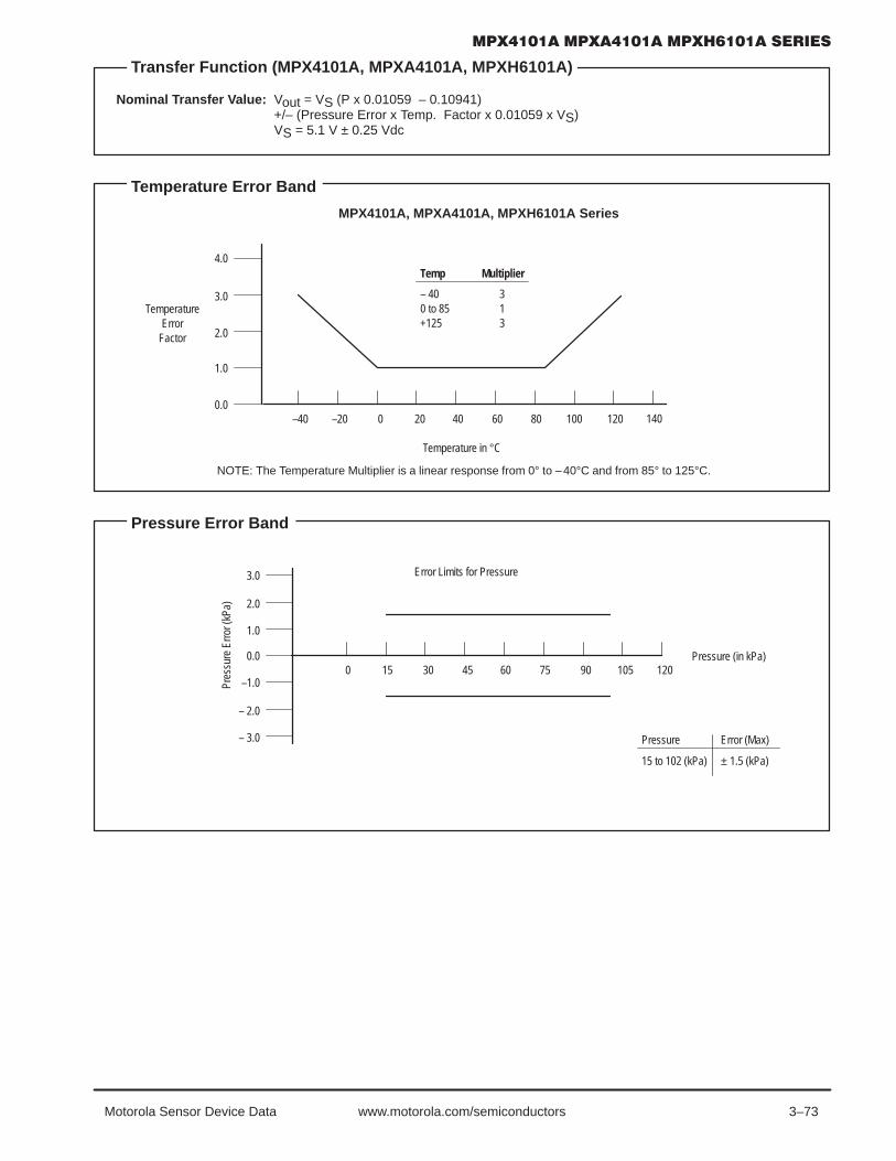
3–73Motorola Sensor Device Data www.motorola.com/semiconductors
Nominal Transfer Value: Vout = VS (P x 0.01059 – 0.10941)+/– (Pressure Error x Temp. Factor x 0.01059 x VS)VS = 5.1 V ± 0.25 Vdc
Transfer Function (MPX4101A, MPXA4101A, MPXH 6101A)
Temperature Error Band
Temperature in °C
4.0
3.0
2.0
0.0
1.0
–40 –20 0 20 40 60 12010080
MPX4101A, MPXA4101A, MPXH6101A Series
Temp Multiplier
– 40 30 to 85 1+125 3
TemperatureError
Factor
140
NOTE: The Temperature Multiplier is a linear response from 0° to –40°C and from 85° to 125°C.
Pressure Error Band
Error Limits for Pressure
Pressure (in kPa)
3.0
2.0
1.0
–1.0
– 2.0
– 3.0
0.00 15 30 45 60 75 90 105 120
Pres
sure
Erro
r (kP
a)
Pressure Error (Max)
15 to 102 (kPa) ± 1.5 (kPa)

3–74 Motorola Sensor Device Datawww.motorola.com/semiconductors
PRESSURE (P1)/VACUUM (P2) SIDE IDENTIFICATION TABLE
Motorola designates the two sides of the pressure sensoras the Pressure (P1) side and the Vacuum (P2) side. ThePressure (P1) side is the side containing fluorosilicone gelwhich protects the die from harsh media. The Motorola pres-
sure sensor is designed to operate with positive differentialpressure applied, P1 > P2.
The Pressure (P1) side may be identified by using the tablebelow:
Part Number Case TypePressure (P1)Side Identifier
MPX4101A 867 Stainless Steel Cap
MPXA4101AC6U 482A Side with Port Attached
MPXH6101A6U 1317 Stainless Steel Cap
MPXH6101A6T1 1317 Stainless Steel Cap
ORDERING INFORMATION — UNIBODY PACKAGE
The MPX4101A series MAP silicon pressure sensors are available in the Basic Element, or with pressure port fittings thatprovide mounting ease and barbed hose connections.
MPX Series
Device Type Options Case Type Order Number Device Marking
Basic Element Absolute, Element Only 867 MPX4101A MPX4101A
ORDERING INFORMATION — SMALL OUTLINE PACKAGE
Device Type Options Case No. MPX Series Order No. Packing Options Marking
Ported Element Absolute, Axial Port 482A MPXA4101AC6U Rails MPXA4101A
ORDERING INFORMATION — SUPER SMALL OUTLINE PACKAGE
Device Type Options Case No. MPX Series Order No. Packing Options Marking
Basic Element Absolute, Element Only 1317 MPXH6101A6U Rails MPXH6101A
Basic Element Absolute, Element Only 1317 MPXH6101A6T1 Tape and Reel MPXH6101A
INFORMATION FOR USING THE SMALL OUTLINE PACKAGES
MINIMUM RECOMMENDED FOOTPRINT FOR SURFACE MOUNTED APPLICATIONS
Surface mount board layout is a critical portion of the totaldesign. The footprint for the surface mount packages mustbe the correct size to ensure proper solder connection inter-face between the board and the package. With the correct
footprint, the packages will self align when subjected to asolder reflow process. It is always recommended to designboards with a solder mask layer to avoid bridging and short-ing between solder pads.
0.66016.76
0.060 TYP 8X1.52
0.100 TYP 8X2.54
0.100 TYP 8X2.54
0.3007.62
Figure 5. SOP Footprint (Case 482)
inchmm SCALE 2:1
Figure 6. SSOP Footprint (Case 1317)
0.027 TYP 8X0.69
0.053 TYP 8X1.35
inchmm
0.3879.83
0.1503.81
0.0501.27TYP

3–75Motorola Sensor Device Data www.motorola.com/semiconductors
$"$ "##%" # " " # %$ "##%"!!$ #! $ !"$%" !#$ "$
The Motorola MPX4105A series Manifold Absolute Pressure (MAP) sensor for enginecontrol is designed to sense absolute air pressure within the intake manifold. Thismeasurement can be used to compute the amount of fuel required for each cylinder.
Motorola’s MAP sensor integrates on–chip, bipolar op amp circuitry and thin filmresistor networks to provide a high output signal and temperature compensation. Thesmall form factor and high reliability of on–chip integration make the Motorola MAPsensor a logical and economical choice for the automotive system designer.
The MPX4105A series piezoresistive transducer is a state–of–the–art, monolithic, signalconditioned, silicon pressure sensor. This sensor combines advanced micromachiningtechniques, thin film metallization, and bipolar semiconductor processing to provide anaccurate, high level analog output signal that is proportional to applied pressure.
Figure 1 shows a block diagram of the internal circuitry integrated on a pressuresensor chip.
Features
• 1.8% Maximum Error Over 0° to 85°C• Specifically Designed for Intake Manifold Absolute
Pressure Sensing in Engine Control Systems
• Temperature Compensated Over –40 to +125°C• Durable Epoxy Unibody Element
Application Examples
• Manifold Sensing for Automotive Systems
• Ideally Suited for Microprocessor or Microcontroller–Based Systems
• Also Ideal for Non–Automotive Applications
Figure 1. Fully Integrated Pressure Sensor Schematic
VS
SENSINGELEMENT
Vout
GND
THIN FILMTEMPERATURECOMPENSATION
ANDGAIN STAGE #1
GAIN STAGE #2AND
GROUNDREFERENCE
SHIFT CIRCUITRY
PINS 4, 5 AND 6 ARE NO CONNECTS FORUNIBODY DEVICE
SEMICONDUCTOR TECHNICAL DATA
MPX4105ACASE 867
UNIBODY PACKAGE
PIN NUMBER
NOTE: Pins 4, 5, and 6 are internaldevice connections. Do not connectto external circuitry or ground. Pin 1is noted by the notch in the lead.
1
2
3
Vout
Gnd
VS
4
5
6
N/C
N/C
N/C
INTEGRATEDPRESSURE SENSOR
15 to 105 kPa(2.2 to 15.2 psi)
0.3 to 4.9 V Output
REV 4

3–76 Motorola Sensor Device Datawww.motorola.com/semiconductors
MAXIMUM RATINGS(NOTE)
Parametrics Symbol Value Units
Maximum Pressure (P1 P2) Pmax 400 kPa
Storage Temperature Tstg –40° to +125° °C
Operating Temperature TA –40° to +125° °C
NOTE: Exposure beyond the specified limits may cause permanent damage or degradation to the device.
OPERATING CHARACTERISTICS (VS = 5.1 Vdc, TA = 25°C unless otherwise noted. Decoupling circuit shown in Figure 3 required tomeet specification.)
Characteristic Symbol Min Typ Max Unit
Pressure Range POP 15 — 105 kPa
Supply Voltage(1) VS 4.85 5.1 5.35 Vdc
Supply Current Io — 7.0 10 mAdc
Minimum Pressure Offset(2) (0 to 85°C) Voff 0.184 0.306 0.428 Vdc
Full Scale Output(3) (0 to 85°C) VFSO 4.804 4.896 4.988 Vdc
Full Scale Span(4) (0 to 85°C) VFSS — 4.590 — Vdc
Accuracy(5) (0 to 85°C) — — — ±1.8 %VFSS
Sensitivity ∆V/∆P — 51 — mV/kPa
Response Time(6) tR — 1.0 — ms
Output Source Current at Full Scale Output Io+ — 0.1 — mAdc
Warm–up Time(7) — — 15 — ms
Offset Stability(8) — — ±0.65 — %VFSS
NOTES:1. Device is ratiometric within this specified excitation range.2. Offset (Voff) is defined as the output voltage at the minimum rated pressure.3. Full Scale Output (VFSO) is defined as the output voltage at the maximum or full rated pressure.4. Full Scale Span (VFSS) is defined as the algebraic difference between the output voltage at full rated pressure and the output voltage at the
minimum rated pressure.5. Accuracy is the deviation in actual output from nominal output over the entire pressure range and temperature range as a percent of span
at 25°C due to all sources of error including the following:• Linearity: Output deviation from a straight line relationship with pressure over the specified pressure range.• Temperature Hysteresis: Output deviation at any temperature within the operating temperature range, after the temperature is
cycled to and from the minimum or maximum operating temperature points, with minimum specifiedpressure applied.
• Pressure Hysteresis: Output deviation at any pressure within the specified range, when this pressure is cycled to and from minimum or maximum rated pressure at 25°C.
• TcSpan: Span deviation per °C over the temperature range of 0° to 85°C, as a percent of span at 25°C.• TcOffset: Output deviation per °C with minimum pressure applied, over the temperature range of 0° to 85°C.
6. Response Time is defined as the time for the incremental change in the output to go from 10% to 90% of its final value when subjected toa specified step change in pressure.
7. Warm–up Time is defined as the time required for the product to meet the specified output voltage.8. Offset Stability is the product’s output deviation when subjected to 1000 hours of Pulsed Pressure, Temperature Cycling with Bias Test.
MECHANICAL CHARACTERISTICS
Characteristics Typ Unit
Weight, Basic Element (Case 867) 4.0 grams

3–77Motorola Sensor Device Data www.motorola.com/semiconductors
Figure 2. Cross–Sectional Diagram(not to scale)
ÉÉÉÉÉÉÉÉÉÉÉÉÉÉÉÉÉÉÉÉÉÉÉÉÉÉÉÉÉÉÉÉÉÉÉÉÉÉÉÉÉÉÉÉ
FLUORO SILICONEGEL DIE COAT
WIRE BOND
LEADFRAME
STAINLESSSTEEL CAP
EPOXYPLASTIC
CASE
DIEBONDABSOLUTE ELEMENT
SEALED VACUUM REFERENCE
DIE P1
P2
Figure 3. Recommended power supply decouplingand output filtering.
For additional output filtering, please refer toApplication Note AN1646.
1.0 F
IPS
470 pF
OUTPUT
Vs
5 V
0.01 F GND
Vout
Figure 2 illustrates an absolute sensing chip in the basicchip carrier (Case 867).
A fluorosilicone gel isolates the die surface and wirebonds from the environment, while allowing the pressuresignal to be transmitted to the sensor diaphragm. TheMPX4105A series pressure sensor operating characteristics,internal reliability and qualification tests are based on use ofdry air as the pressure media. Media other than dry air may
have adverse effects on sensor performance and long–termreliability. Contact the factory for information regarding me-dia compatibility in your application.
Figure 3 shows the recommended decoupling circuit for in-terfacing the output of the integrated sensor to the A/D inputof a microprocessor or microcontroller. Proper decoupling ofthe power supply is recommended.
OU
TPU
T (V
olts
)
5.0
4.5
4.0
3.5
3.0
Pressure (ref: to sealed vacuum) in kPa
MAX
MIN
0 5 10 15 20 25 30 35 40 45 50 55 60 65 70 75 80 85 90 95 100
2.5
2.0
1.5
1.0
0.5
0
105
Figure 4. Output versus Absolute Pressure
TEMP = 0 to 85°C15 kPA TO 105 kPAMPX4105A
TRANSFER FUNCTION:Vout = Vs* (0.01*P–0.09) ± ErrorVS = 5.1 Vdc
110
TYP
Figure 4 shows the sensor output signal relative to pres-sure input. Typical minimum and maximum output curvesare shown for operation over a temperature range of 0° to
85°C. The output will saturate outside of the specifiedpressure range.

3–78 Motorola Sensor Device Datawww.motorola.com/semiconductors
Transfer Function (MPX4105A)
Nominal Transfer Value: Vout = VS (P x 0.01 – 0.09)+/– (Pressure Error x Temp. Factor x 0.01 x VS)VS = 5.1 V ± 0.25 Vdc
Temperature Error BandMPX4105A Series
Break Points
Temp Multiplier
– 40 3.0– 20 1.50 to 85 1.0125 2.5
Temperature in C°
4.0
3.0
2.0
0.0
1.0
–40 –20 0 20 40 60 14012010080
TemperatureError
Factor
NOTE: The Temperature Multiplier is a linear response from –40°C to –20°C, –20°C to 0°C, and from 85°C to 125°C
Pressure Error Band
Error Limits for Pressure3.0
2.0
1.0
–1.0
– 2.0
– 3.0
0.020 40 60 80 100 120
Pressure (in kPa)
Pres
sure
Erro
r (kP
a)
Pressure Error (Max)
40 to 94 (kPa) ± 1.5 (kPa)15 (kPa) ± 2.4 (kPa)105 (kPa) ± 1.8 (kPa)
ORDERING INFORMATION — UNIBODY PACKAGE
Device Type Options Case No MPX Series Order No MarkingDevice Type Options Case No. MPX Series Order No. Marking
Basic Element Absolute Element 867 MPX4105A MPX4105ABasic Element Absolute, Element 867 MPX4105A MPX4105A

3–79Motorola Sensor Device Data www.motorola.com/semiconductors
$"$ "##%" # " " # %$ "##%"$$" " " $" !!$ #! $ !"$%" !#$ "$
Motorola’s MPX4115A/MPXA4115A series sensor integrates on–chip, bipolar op ampcircuitry and thin film resistor networks to provide a high output signal and temperaturecompensation. The small form factor and high reliability of on–chip integration make theMotorola pressure sensor a logical and economical choice for the system designer.
The MPX4115A/MPXA4115A series piezoresistive transducer is a state–of–the–art,monolithic, signal conditioned, silicon pressure sensor. This sensor combines advancedmicromachining techniques, thin film metallization, and bipolar semiconductor processing toprovide an accurate, high level analog output signal that is proportional to applied pressure.
Figure 1 shows a block diagram of the internal circuitry integrated on a pressuresensor chip.
Features
• 1.5% Maximum Error over 0° to 85°C• Ideally suited for Microprocessor or Microcontroller–
Based Systems
• Temperature Compensated from –40° to +125°C• Durable Epoxy Unibody Element or Thermoplastic
(PPS) Surface Mount Package
Application Examples
• Aviation Altimeters
• Industrial Controls
• Engine Control
• Weather Stations and Weather Reporting Devices
Figure 1. Fully Integrated Pressure SensorSchematic
VS
SENSINGELEMENT
Vout
GND
THIN FILMTEMPERATURECOMPENSATION
ANDGAIN STAGE #1
GAIN STAGE #2AND
GROUNDREFERENCE
SHIFT CIRCUITRY
PINS 1, 5, 6, 7 AND 8 ARE NO CONNECTSFOR SMALL OUTLINE PACKAGE DEVICE
PINS 4, 5 AND 6 ARE NO CONNECTS FORUNIBODY DEVICE
SEMICONDUCTOR TECHNICAL DATA
INTEGRATEDPRESSURE SENSOR
15 to 115 kPa (2.2 to 16.7 psi)0.2 to 4.8 Volts Output
PIN NUMBER
NOTE: Pins 4, 5, and 6 are internaldevice connections. Do not connectto external circuitry or ground. Pin 1is noted by the notch in the lead.
MPX4115ACASE 867
MPX4115APCASE 867B
1
2
3
Vout
Gnd
VS
4
5
6
N/C
N/C
N/C
UNIBODY PACKAGE
PIN NUMBER
NOTE: Pins 1, 5, 6, 7, and 8 areinternal device connections. Do notconnect to external circuitry orground. Pin 1 is noted by the notch inthe lead.
1
2
3
N/C
VSGnd
5
6
7
N/C
N/C
N/C
MPXA4115A6UCASE 482
MPXA4115AC6UCASE 482A
4 Vout 8 N/C
SMALL OUTLINE PACKAGE
MPX4115ASCASE 867E
REV 4

3–80 Motorola Sensor Device Datawww.motorola.com/semiconductors
MAXIMUM RATINGS(NOTE)
Parametrics Symbol Value Units
Maximum Pressure (P1 P2) Pmax 400 kPa
Storage Temperature Tstg –40° to +125° °C
Operating Temperature TA –40° to +125° °C
NOTE: Exposure beyond the specified limits may cause permanent damage or degradation to the device.
OPERATING CHARACTERISTICS (VS = 5.1 Vdc, TA = 25°C unless otherwise noted, P1 P2. Decoupling circuit shown in Figure 3required to meet Electrical Specifications.)
Characteristic Symbol Min Typ Max Unit
Pressure Range POP 15 — 115 kPa
Supply Voltage(1) VS 4.85 5.1 5.35 Vdc
Supply Current Io — 7.0 10 mAdc
Minimum Pressure Offset(2) (0 to 85°C)@ VS = 5.1 Volts
Voff 0.135 0.204 0.273 Vdc
Full Scale Output(3) (0 to 85°C)@ VS = 5.1 Volts
VFSO 4.725 4.794 4.863 Vdc
Full Scale Span(4) (0 to 85°C)@ VS = 5.1 Volts
VFSS 4.521 4.590 4.659 Vdc
Accuracy(5) (0 to 85°C) — — — ±1.5 %VFSS
Sensitivity V/P — 45.9 — mV/kPa
Response Time(6) tR — 1.0 — ms
Output Source Current at Full Scale Output Io+ — 0.1 — mAdc
Warm–Up Time(7) — — 20 — ms
Offset Stability(8) — — ±0.5 — %VFSS
NOTES:1. Device is ratiometric within this specified excitation range.2. Offset (Voff) is defined as the output voltage at the minimum rated pressure.3. Full Scale Output (VFSO) is defined as the output voltage at the maximum or full rated pressure.4. Full Scale Span (VFSS) is defined as the algebraic difference between the output voltage at full rated pressure and the output voltage at the
minimum rated pressure.5. Accuracy is the deviation in actual output from nominal output over the entire pressure range and temperature range as a percent of span
at 25°C due to all sources of error including the following:• Linearity: Output deviation from a straight line relationship with pressure over the specified pressure range.• Temperature Hysteresis: Output deviation at any temperature within the operating temperature range, after the temperature is
cycled to and from the minimum or maximum operating temperature points, with zero differentialpressure applied.
• Pressure Hysteresis: Output deviation at any pressure within the specified range, when this pressure is cycled to and from minimum or maximum rated pressure at 25°C.
• TcSpan: Output deviation over the temperature range of 0° to 85°C, relative to 25°C.• TcOffset: Output deviation with minimum pressure applied, over the temperature range of 0° to 85°C, relative
to 25°C.6. Response Time is defined as the time for the incremental change in the output to go from 10% to 90% of its final value when subjected to
a specified step change in pressure.7. Warm–up Time is defined as the time required for the product to meet the specified output voltage after the pressure has been stabilized.8. Offset Stability is the product’s output deviation when subjected to 1000 cycles of Pulsed Pressure, Temperature Cycling with Bias Test.
MECHANICAL CHARACTERISTICS
Characteristics Typ Unit
Weight, Basic Element (Case 867) 4.0 grams
Weight, Small Outline Package (Case 482) 1.5 grams

3–81Motorola Sensor Device Data www.motorola.com/semiconductors
Figure 2. Cross Sectional Diagram SOP(not to scale)
Figure 3. Recommended power supply decouplingand output filtering.
For additional output filtering, please refer toApplication Note AN1646.
1.0 F
IPS
470 pF
OUTPUT
Vs
5 V
0.01 F GND
Vout
WIRE BOND
STAINLESSSTEEL CAP
THERMOPLASTICCASE
DIE BONDSEALED VACUUM REFERENCE
DIE
P1
FLUORO SILICONEGEL DIE COAT
LEADFRAME
ABSOLUTE ELEMENT
Figure 2 illustrates the absolute sensing chip in the basicchip carrier (Case 482).
Figure 3 shows the recommended decoupling circuit forinterfacing the output of the integrated sensor to the A/D in-put of a microprocessor or microcontroller. Proper decoup-ling of the power supply is recommended.
OU
TPU
T (V
olts
)
5.0
4.5
4.0
3.5
3.0
Pressure (ref: to sealed vacuum) in kPa
TYP
MAX
MIN
5 10 15 20 25 30 35 40 45 50 55 60 65 70 75 80 85 90 95 100
105
2.5
2.0
1.5
1.0
0.5
0
110
Figure 4. Output versus Absolute Pressure
TRANSFER FUNCTION:Vout = Vs* (.009*P–.095) ± ErrorVS = 5.1 VdcTEMP = 0 to 85°C
115
120
Figure 4 shows the sensor output signal relative to pres-sure input. Typical minimum and maximum output curvesare shown for operation over 0 to 85°C temperature range.The output will saturate outside of the rated pressure range.
A fluorosilicone gel isolates the die surface and wirebonds from the environment, while allowing the pressuresignal to be transmitted to the silicon diaphragm. The
MPX4115A/MPXA4115A series pressure sensor operatingcharacteristics, internal reliability and qualification tests arebased on use of dry air as the pressure media. Media otherthan dry air may have adverse effects on sensor perfor-mance and long–term reliability. Contact the factory forinformation regarding media compatibility in your application.

3–82 Motorola Sensor Device Datawww.motorola.com/semiconductors
Transfer Function (MPX4115A, MPXA4115A)
Nominal Transfer Value: Vout = VS x (0.009 x P – 0.095)± (Pressure Error x Temp. Factor x 0.009 x VS)VS = 5.1 ± 0.25 Vdc
Temperature Error BandMPX4115A, MPXA4115A Series
Break Points
Temp Multiplier
– 40 30 to 85 1125 3
Temperature in C°
4.0
3.0
2.0
0.0
1.0
–40 –20 0 20 40 60 14012010080
TemperatureError
Factor
NOTE: The Temperature Multiplier is a linear response from 0°C to –40°C and from 85°C to 125°C
Pressure Error Band
Error Limits for Pressure3.0
2.0
1.0
–1.0
– 2.0
– 3.0
0.020 Pressure (in kPa)
Pres
sure
Erro
r (kP
a)
Pressure Error (Max)
15 to 115 (kPa) ± 1.5 (kPa)
40 60 80 100 120
ORDERING INFORMATION — UNIBODY PACKAGE
Device Type Options Case No. MPX Series Order No. Marking
Basic Element Absolute, Element Only 867 MPX4115A MPX4115A
Ported Elements Absolute, Ported 867B MPX4115AP MPX4115AP
Absolute, Stove Pipe Port 867E MPX4115AS MPX4115A
ORDERING INFORMATION — SMALL OUTLINE PACKAGE
Device Type Options Case No. MPX Series Order No. Packing Options Marking
Basic Element Absolute, Element Only 482 MPXA4115A6U Rails MPXA4115A
Absolute, Element Only 482 MPXA4115A6T1 Tape and Reel MPXA4115A
Ported Element Absolute, Axial Port 482A MPXA4115AC6U Rails MPXA4115A
Absolute, Axial Port 482A MPXA4115AC6T1 Tape and Reel MPXA4115A

3–83Motorola Sensor Device Data www.motorola.com/semiconductors
INFORMATION FOR USING THE SMALL OUTLINE PACKAGE (CASE 482)
MINIMUM RECOMMENDED FOOTPRINT FOR SURFACE MOUNTED APPLICATIONS
Surface mount board layout is a critical portion of the totaldesign. The footprint for the surface mount packages mustbe the correct size to ensure proper solder connection inter-face between the board and the package. With the correct
fottprint, the packages will self–align when subjected to asolder reflow process. It is always recommended to designboards with a solder mask layer to avoid bridging and short-ing between solder pads.
0.66016.76
0.060 TYP 8X1.52
0.100 TYP 8X2.54
0.100 TYP 8X2.54
0.3007.62
Figure 5. SOP Footprint (Case 482)
inchmm SCALE 2:1

3–84 Motorola Sensor Device Datawww.motorola.com/semiconductors
#!# !""$! "!! "$# !""$! #" # !#$! "# !#
The Motorola MPX4200A series Manifold Absolute Pressure (MAP) sensor for turboboost engine control is designed to sense absolute air pressure within the intakemanifold. This measurement can be used to compute the amount of fuel required foreach cylinder.
The MPX4200A series sensor integrates on–chip, bipolar op amp circuitry and thin filmresistor networks to provide a high level analog output signal and temperaturecompensation. The small form factor and reliability of on–chip integration make theMotorola MAP sensor a logical and economical choice for automotive system designers.
Features
• Specifically Designed for Intake Manifold Absolute Pressure Sensing in EngineControl Systems
• Patented Silicon Shear Stress Strain Gauge
• Temperature Compensated Over –40° to +125°C• Offers Reduction in Weight and Volume Compared to Existing Hybrid Modules
• Durable Epoxy Unibody Element
Application Examples
• Manifold Sensing for Automotive Systems
• Ideally suited for Microprocessor or Microcontroller–Based Systems
• Also ideal for Non–Automotive Applications
PINS 4, 5 AND 6 ARE NO CONNECTS
Figure 1. Fully Integrated Pressure Sensor Schematic
VS
SENSINGELEMENT Vout
GND
THIN FILMTEMPERATURECOMPENSATION
ANDGAIN STAGE #1
GAIN STAGE #2AND
GROUNDREFERENCE
SHIFT CIRCUITRY
SEMICONDUCTOR TECHNICAL DATA
INTEGRATEDPRESSURE SENSOR
20 to 200 kPa (2.9 to 29 psi)0.3 to 4.9 V OUTPUT
PIN NUMBER
NOTE: Pins 4, 5, and 6 are internaldevice connections. Do not connectto external circuitry or ground. Pin 1is noted by the notch in the lead.
MPX4200ACASE 867
1
2
3
Vout
Gnd
VS
4
5
6
N/C
N/C
N/C
Rev 1

3–85Motorola Sensor Device Data www.motorola.com/semiconductors
MAXIMUM RATINGS(NOTE)
Parametrics Symbol Value Unit
Maximum Pressure (P1 > P2) Pmax 800 kPa
Storage Temperature Tstg –40 to +125 °C
Operating Temperature TA –40 to +125 °C
NOTE: Exposure beyond the specified limits may cause permanent damage or degradation to the device.
OPERATING CHARACTERISTICS (VS = 5.1 Vdc, TA = 25°C unless otherwise noted, P1 > P2. Decoupling circuit shown in Figure 3required to meet electrical specifications.)
Characteristic Symbol Min Typ Max Unit
Pressure Range(1) POP 20 — 200 kPa
Supply Voltage(2) VS 4.85 5.1 5.35 Vdc
Supply Current Io — 7.0 10 mAdc
Minimum Pressure Offset(3) (0 to 85°C)@ VS = 5.1 Volts
Voff 0.199 0.306 0.413 Vdc
Full Scale Output(4) (0 to 85°C)@ VS = 5.1 Volts
VFSO 4.725 4.896 4.978 Vdc
Full Scale Span(5) (0 to 85°C)@ VS = 5.1 Volts
VFSS — 4.590 — Vdc
Accuracy(6) (0 to 85°C) — — — ±1.5 %VFSS
Sensitivity V/P — 25.5 — mV/kPa
Response Time(7) tR — 1.0 — ms
Output Source Current at Full Scale Output lo+ — 0.1 — mAdc
Warm–Up Time(8) — — 20 — ms
Offset Stability(9) — — ±0.5 — %VFSS
NOTES:1. 1.0 kPa (kiloPascal) equals 0.145 psi.2. Device is ratiometric within this specified excitation range.3. Offset (Voff) is defined as the output voltage at the minimum rated pressure.4. Full Scale Output (VFSO) is defined as the output voltage at the maximum or full rated pressure.5. Full Scale Span (VFSS) is defined as the algebraic difference between the output voltage at full rated pressure and the output voltage at the
minimum rated pressure.6. Accuracy (error budget) consists of the following:
• Linearity: Output deviation from a straight line relationship with pressure over the specified pressure range.• Temperature Hysteresis: Output deviation at any temperature within the operating temperature range, after the temperature is
cycled to and from the minimum or maximum operating temperature points, with zero differential pressureapplied.
• Pressure Hysteresis: Output deviation at any pressure within the specified range, when this pressure is cycled to and from theminimum or maximum rated pressure, at 25°C.
• TcSpan: Output deviation over the temperature range of 0° to 85°C, relative to 25°C.• TcOffset: Output deviation with minimum rated pressure applied, over the temperature range of 0° to 85°C, relative
to 25°C.• Variation from Nominal: The variation from nominal values, for Offset or Full Scale Span, as a percent of VFSS at 25°C.
7. Response Time is defined as the time for the incremental change in the output to go from 10% to 90% of its final value when subjected toa specified step change in pressure.
8. Warm–up Time is defined as the time required for the product to meet the specified output voltage after the Pressure has been stabilized.9. Offset Stability is the product’s output deviation when subjected to 1000 hours of Pulsed Pressure, Temperature Cycling with Bias Test.
MECHANICAL CHARACTERISTICS
Characteristics Typ Unit
Weight, Basic Element (Case 867) 4.0 grams

3–86 Motorola Sensor Device Datawww.motorola.com/semiconductors
Figure 2. Cross–Sectional Diagram(Not to Scale)
ÉÉÉÉÉÉÉÉÉÉÉÉÉÉÉÉÉÉÉÉÉÉÉÉÉÉÉÉÉÉÉÉÉÉÉÉÉÉÉÉÉÉÉÉÉÉÉÉÉÉÉÉÉÉÉ
SILICONEDIE COAT
WIRE BOND
STAINLESS STEELMETAL COVER
RTV DIEBOND
DIE P1
P2
EPOXYCASE
LEAD FRAME
SEALED VACUUM REFERENCE
1.0 F
IPS
470 pF
OUTPUT
Vs
5 V
0.01 F GND
Vout
Figure 3. Recommended power supply decouplingand output filtering.
For additional output filtering, please refer toApplication Note AN1646.
Figure 2 illustrates the absolute sensing chip in the basicchip carrier (Case 867). A fluorosilicone gel isolates thedie surface and wire bonds from the environment, whileallowing the pressure signal to be transmitted to the sen-sor diaphragm. The MPX4200A series pressure sensoroperating characteristics, and internal reliability and quali-fication tests are based on use of dry air as the pressuremedia. Media, other than dry air, may have adverse ef-fects on sensor performance and long–term reliability.Contact the factory for information regarding media com-patibility in your application.
Figure 3 shows the recommended decoupling circuit forinterfacing the output of the integrated sensor to the A/D in-put of a microprocessor or microcontroller. Proper decoup-ling of the power supply is recommended.
Figure 4 shows the sensor output signal relative to pres-sure input. Typical minimum and maximum output curvesare shown for operation over temperature range of 0° to85°C. The output will saturate outside of the specified pres-sure range.
0 10 20 30 50 60 70 80 90 100
200
2100
OU
TPU
T (V
olts
)
5.0
4.5
4.0
3.5
3.0
MAX
MIN
2.5
2.0
1.5
1.0
0.5
Figure 4. Output versus Absolute Pressure
TYP
TRANSFER FUNCTION:Vout = VS* (0.005 x P–0.04) ± ErrorVS = 5.1 VdcTEMP = 0 to 85°C
40 110
120
130
140
150
160
170
180
190

3–87Motorola Sensor Device Data www.motorola.com/semiconductors
ORDERING INFORMATION
Device Type Options Case No. MPX Series Order No. Marking
Basic Element Absolute, Element Case 867 MPX4200A MPX4200A
Transfer Function (MPX4200A)
Nominal Transfer Value: Vout = VS x (0.005 x P – 0.04)Nominal Transfer Value: ± (Pressure Error x Temp. Factor x 0.005 x VS)Nominal Transfer Value: VS = 5.1 ± 0.25 Vdc
Temperature Error Band
Temp Multiplier
– 40 3–18 1.560 to 85 1+125 2
Temperature in C°
4.0
3.0
2.0
0.0
1.0
–40 –20 0 20 40 60 14012010080
MPX4200A Series
TemperatureError
Factor
Pressure Error Band
Pressure in kPa
Pressure Error (Max)
20 kPa ± 4.2 (kPa)40 kPa ± 2.4 (kPa)160 kPa ± 2.4 (kPa)200 kPa ± 3.2 (kPa)
6.0
4.0
2.0
–2.0
– 4.0
– 6.0
60 80 100 120 140 160
Pres
sure
Erro
r (kP
a)
18020 40 200
MPX4200A Series
NOTE: The Temperature Multiplier is a linear response from 0°C to –40°C and from 85°C to 125°C

3–88 Motorola Sensor Device Datawww.motorola.com/semiconductors
$"$ "##%" # " # %$ "##%" # "! $ !"$%" !#$ "$
The Motorola MPX4250A/MPXA4250A series Manifold Absolute Pressure (MAP)sensor for engine control is designed to sense absolute air pressure within the intakemanifold. This measurement can be used to compute the amount of fuel required foreach cylinder.
The MPX4250A/MPXA4250A series piezoresistive transducer is a state–of–the–artmonolithic silicon pressure sensor designed for a wide range of applications, particularlythose employing a microcontroller or microprocessor with A/D inputs. This transducercombines advanced micromachining techniques, thin–film metallization and bipolarprocessing to provide an accurate, high–level analog output signal that is proportional tothe applied pressure. The small form factor and high reliability of on–chip integrationmake the Motorola sensor a logical and economical choice for the automotive systemengineer.
Features
• 1.5% Maximum Error Over 0° to 85°C• Specifically Designed for Intake Manifold Absolute
Pressure Sensing in Engine Control Systems
• Patented Silicon Shear Stress Strain Gauge
• Temperature Compensated Over –40° to +125°C• Offers Reduction in Weight and Volume Compared
to Existing Hybrid Modules
• Durable Epoxy Unibody Element or ThermoplasticSmall Outline, Surface Mount Package
• Ideal for Non–Automotive Applications
Application Examples
• Turbo Boost Engine Control
• Ideally Suited for Microprocessor or Microcontroller–Based Systems
PINS 4, 5, AND 6 ARE NO CONNECTS FORUNIBODY DEVICEPINS 1, 5, 6, 7, AND 8 ARE NO CONNECTSFOR SMALL OUTLINE PACKAGE DEVICE
Figure 1. Fully Integrated Pressure SensorSchematic
VS
SENSINGELEMENT Vout
GND
THIN FILMTEMPERATURECOMPENSATION
ANDGAIN STAGE #1
GAIN STAGE #2AND
GROUNDREFERENCE
SHIFT CIRCUITRY
SEMICONDUCTOR TECHNICAL DATA
PIN NUMBER
NOTE: Pins 1, 5, 6, and 7 are internaldevice connections. Do not connectto external circuitry or ground. Pin 1is noted by the notch in the lead.
1
2
3
N/C
VSGnd
5
6
7
N/C
N/C
N/C
PORT OPTIONCASE 482
PORT OPTIONCASE 482A
4 Vout 8 N/C
SMALL OUTLINE PACKAGE
INTEGRATEDPRESSURE SENSOR
20 to 250 kPa (2.9 to 36.3 psi)0.2 to 4.9 V OUTPUT
PIN NUMBER
NOTE: Pins 4, 5, and 6 are internaldevice connections. Do not connectto external circuitry or ground. Pin 1is noted by the notch in the lead.
BASIC CHIPCARRIER ELEMENTCASE 867, STYLE 1
PORT OPTIONCASE 867B, STYLE 1
1
2
3
Vout
Gnd
VS
4
5
6
N/C
N/C
N/C
UNIBODY PACKAGE
REV 4

3–89Motorola Sensor Device Data www.motorola.com/semiconductors
MAXIMUM RATINGS(1)
Parametrics Symbol Value Unit
Maximum Pressure(2) (P1 > P2) Pmax 1000 kPa
Storage Temperature Tstg –40 to +125 °C
Operating Temperature TA –40 to +125 °C
NOTES:1. TC = 25°C unless otherwise noted.2. Exposure beyond the specified limits may cause permanent damage or degradation to the device.
OPERATING CHARACTERISTICS (VS = 5.1 Vdc, TA = 25°C unless otherwise noted, P1 > P2, Decoupling circuit shown in Figure 3required to meet electrical specifications.)
Characteristic Symbol Min Typ Max Unit
Pressure Range(1) POP 20 — 250 kPa
Supply Voltage(2) VS 4.85 5.1 5.35 Vdc
Supply Current Io — 7.0 10 mAdc
Minimum Pressure Offset(3) (0 to 85°C)@ VS = 5.1 Volts
Voff 0.133 0.204 0.274 Vdc
Full Scale Output(4) (0 to 85°C)@ VS = 5.1 Volts
VFSO 4.826 4.896 4.966 Vdc
Full Scale Span(5) (0 to 85°C)@ VS = 5.1 Volts
VFSS — 4.692 — Vdc
Accuracy(6) (0 to 85°C) — — — ±1.5 %VFSS
Sensitivity ∆V/∆P — 20 — mV/kPa
Response Time(7) tR — 1.0 — msec
Output Source Current at Full Scale Output lo+ — 0.1 — mAdc
Warm–Up Time(8) — — 20 — msec
Offset Stability(9) — — ±0.5 — %VFSS
NOTES:1. 1.0 kPa (kiloPascal) equals 0.145 psi.2. Device is ratiometric within this specified excitation range.3. Offset (Voff) is defined as the output voltage at the minimum rated pressure.4. Full Scale Output (VFSO) is defined as the output voltage at the maximum or full rated pressure.5. Full Scale Span (VFSS) is defined as the algebraic difference between the output voltage at full rated pressure and the output voltage at the
minimum rated pressure.6. Accuracy (error budget) consists of the following:
• Linearity: Output deviation from a straight line relationship with pressure over the specified pressure range.• Temperature Hysteresis: Output deviation at any temperature within the operating temperature range, after the temperature is
cycled to and from the minimum or maximum operating temperature points, with zero differential pressureapplied.
• Pressure Hysteresis: Output deviation at any pressure within the specified range, when this pressure is cycled to and from theminimum or maximum rated pressure, at 25°C.
• TcSpan: Output deviation over the temperature range of 0° to 85°C, relative to 25°C.• TcOffset: Output deviation with minimum rated pressure applied, over the temperature range of 0° to 85°C, relative
to 25°C.• Variation from Nominal: The variation from nominal values, for Offset or Full Scale Span, as a percent of VFSS, at 25°C.
7. Response Time is defined as the time for the incremental change in the output to go from 10% to 90% of its final value when subjected toa specified step change in pressure.
8. Warm–up is defined as the time required for the product to meet the specified output voltage after the Pressure has been stabilized.9. Offset stability is the product’s output deviation when subjected to 1000 hours of Pulsed Pressure, Temperature Cycling with Bias Test.
MECHANICAL CHARACTERISTICS
Characteristics Typ Unit
Weight, Basic Element (Case 867) 4.0 Grams
Weight, Small Outline Package (Case 482) 1.5 Grams

3–90 Motorola Sensor Device Datawww.motorola.com/semiconductors
Figure 2. Cross–Sectional Diagram(Not to Scale)
ÉÉÉÉÉÉÉÉÉÉÉÉÉÉÉÉÉÉÉÉÉÉÉÉÉÉÉÉÉÉÉÉÉÉÉÉÉÉÉÉÉÉÉÉÉÉÉÉÉÉÉÉÉÉÉ
FLUOROSILICONEDIE COAT
WIRE BOND
STAINLESS STEELMETAL COVER
RTV DIEBOND
DIE P1
P2
EPOXYCASE
LEAD FRAME
SEALED VACUUM REFERENCE
1.0 F
IPS
470 pF
OUTPUT
Vs
5 V
0.01 F GND
Vout
Figure 3. Recommended power supply decouplingand output filtering.
For additional output filtering, please refer toApplication Note AN1646.
Figure 2 illustrates the absolute pressure sensing chip inthe basic chip carrier (Case 867). A fluorosilicone gel iso-lates the die surface and wire bonds from the environment,while allowing the pressure signal to be transmitted to thesensor diaphragm.
The MPX4250A/MPXA4250A series pressure sensor op-erating characteristics and internal reliability and qualifica-tion tests are based on use of dry air as the pressuremedia. Media, other than dry air, may have adverse ef-fects on sensor performance and long–term reliability.
Contact the factory for information regarding media com-patibility in your application.
Figure 3 shows the recommended decoupling circuit for in-terfacing the output of the integrated sensor to the A/D inputof a microprocessor or microcontroller.
Figure 4 shows the sensor output signal relative to pres-sure input. Typical, minimum, and maximum output curvesare shown for operation over temperature range of 0° to85°C using the decoupling circuit shown in Figure 3. Theoutput will saturate outside of the specified pressure range.
0
OU
TPU
T (V
olts
)
5.0
4.5
4.0
3.5
3.0
PRESSURE (ref: to sealed vacuum) in kPa
MAX
MIN
0 10 20 30 40 50 60 70 80 90 100
120
130
140
150
160
170
180
190
200
210
220
230
2.5
2.0
1.5
1.0
0.5
240
250
260
110
TYP
TRANSFER FUNCTION:Vout = VS* (0.004 x P–0.04) ± ErrorVS = 5.1 VdcTEMP = 0 to 85°C
Figure 4. Output versus Absolute Pressure

3–91Motorola Sensor Device Data www.motorola.com/semiconductors
Transfer Function
Nominal Transfer Value: Vout = VS (P x 0.004 – 0.04)Nominal Transfer Value: +/– (Pressure Error x Temp. Factor x 0.004 x VS)Nominal Transfer Value: VS = 5.1 V ± 0.25 Vdc
Temperature Error Band
Temp Multiplier
– 40 30 to 85 1+125 3
Temperature in C°
4.0
3.0
2.0
0.0
1.0
–40 –20 0 20 40 60 14012010080
TemperatureError
Factor
Pressure Error Band
Pressure Error (Max)
20 to 250 kPa ± 3.45 (kPa)
NOTE: The Temperature Multiplier is a linear response from 0° to –40°C and from 85° to 125°C.
Pressure(kPa)75 100 125 150 175 200 22525 50 250
4.0
3.0
2.0
1.0
0
–1.0
–2.0
–3.0
–4.0
–5.0
5.0
0
PressureError(kPa)

3–92 Motorola Sensor Device Datawww.motorola.com/semiconductors
ORDERING INFORMATION – UNIBODY PACKAGE (CASE 867)
The MPX4250A series pressure sensors are available in the basic element package or with pressureport fittings that provide mounting ease and barbed hose connections.
Device Type/Order No. Options Case No. Marking
MPX4250A Basic Element 867 MPX4250A
MPX4250AP Ported Element 867B MPX4250AP
ORDERING INFORMATION – SMALL OUTLINE PACKAGE (CASE 482)
The MPXA4250A series pressure sensors are available in the basic element package or with apressure port fitting. Two packing options are offered for each type.
Device Type/Order No. Case No. Packing Options Device Marking
MPXA4250A6U 482 Rails MPXA4250A
MPXA4250A6T1 482 Tape and Reel MPXA4250A
MPXA4250AC6U 482A Rails MPXA4250A
MPXA4250AC6T1 482A Tape and Reel MPXA4250A
INFORMATION FOR USING THE SMALL OUTLINE PACKAGE (CASE 482)
MINIMUM RECOMMENDED FOOTPRINT FOR SURFACE MOUNTED APPLICATIONS
Surface mount board layout is a critical portion of the totaldesign. The footprint for the surface mount packages mustbe the correct size to ensure proper solder connection inter-face between the board and the package. With the correct
fottprint, the packages will self align when subjected to asolder reflow process. It is always recommended to designboards with a solder mask layer to avoid bridging and short-ing between solder pads.
0.66016.76
0.060 TYP 8X1.52
0.100 TYP 8X2.54
0.100 TYP 8X2.54
0.3007.62
Figure 5. SOP Footprint (Case 482)
inchmm SCALE 2:1

3–93Motorola Sensor Device Data www.motorola.com/semiconductors
$"$ "##%" # "! $ !"$%" !#$ "$
The MPX4250D series piezoresistive transducer is a state–of–the–art monolithicsilicon pressure sensor designed for a wide range of applications, particularly thoseemploying a microcontroller or microprocessor with A/D inputs. This transducercombines advanced micromachining techniques, thin–film metallization, and bipolarprocessing to provide an accurate, high–level analog output signal that is proportional tothe applied pressure. The small form factor and high reliability of on–chip integrationmake the Motorola sensor a logical and economical choice for the automotive systemengineer.
Features
• Differential and Gauge Applications Available
• 1.4% Maximum Error Over 0° to 85°C• Patented Silicon Shear Stress Strain Gauge
• Temperature Compensated Over –40° to +125°C• Offers Reduction in Weight and Volume Compared to Existing Hybrid Modules
• Durable Epoxy Unibody Element
Applications
• Ideally Suited for Microprocessor or Microcontroller–Based Systems
PINS 4, 5 AND 6 ARE NO CONNECTS FORUNIBODY DEVICE
Figure 1. Fully Integrated Pressure Sensor Schematic
VS
SENSINGELEMENT Vout
GND
THIN FILMTEMPERATURECOMPENSATION
ANDGAIN STAGE #1
GAIN STAGE #2AND
GROUNDREFERENCE
SHIFT CIRCUITRY
SEMICONDUCTOR TECHNICAL DATA
INTEGRATEDPRESSURE SENSOR
0 to 250 kPa (0 to 36.3 psi)0.2 to 4.9 Volts Output
PIN NUMBER
NOTE: Pins 4, 5, and 6 are internaldevice connections. Do not connectto external circuitry or ground. Pin 1is noted by the notch in the lead.
BASIC CHIPCARRIER ELEMENTCASE 867, STYLE 1
GAUGE PORT OPTIONCASE 867B, STYLE 1
1
2
3
Vout
Gnd
VS
4
5
6
N/C
N/C
N/C
UNIBODY PACKAGE
DUAL PORT OPTIONCASE 867C, STYLE 1
REV 3

3–94 Motorola Sensor Device Datawww.motorola.com/semiconductors
MAXIMUM RATINGS(1)
Parametrics Symbol Value Unit
Maximum Pressure(2) (P1 > P2) Pmax 1000 kPa
Storage Temperature Tstg –40° to +125° °C
Operating Temperature TA –40° to +125° °C
NOTES:1. TC = 25°C unless otherwise noted.2. Exposure beyond the specified limits may cause permanent damage or degradation to the device.
OPERATING CHARACTERISTICS (VS = 5.1 Vdc, TA = 25°C unless otherwise noted, P1 > P2, Decoupling circuit shown in Figure 3required to meet electrical specifications.)
Characteristic Symbol Min Typ Max Unit
Pressure Range(1) POP 0 — 250 kPa
Supply Voltage(2) VS 4.85 5.1 5.35 Vdc
Supply Current Io — 7.0 10 mAdc
Minimum Pressure Offset(3) (0 to 85°C)@ VS = 5.1 Volts
VOFF 0.139 0.204 0.269 Vdc
Full Scale Output(4) (0 to 85°C)@ VS = 5.1 Volts
VFSO 4.844 4.909 4.974 Vdc
Full Scale Span(5) (0 to 85°C)@ VS = 5.1 Volts
VFSS — 4.705 — Vdc
Accuracy(6) (0 to 85°C) — — — ±1.4 %VFSS
Sensitivity ∆V/∆P — 18.8 — mV/kPa
Response Time(7) tR — 1.0 — msec
Output Source Current at Full Scale Output lo+ — 0.1 — mAdc
Warm–Up Time(8) — — 20 — msec
Offset Stability(9) — — ±0.5 — %VFSS
NOTES:1. 1.0 kPa (kiloPascal) equals 0.145 psi.2. Device is ratiometric within this specified excitation range.3. Offset (Voff) is defined as the output voltage at the minimum rated pressure.4. Full Scale Output (VFSO) is defined as the output voltage at the maximum or full rated pressure.5. Full Scale Span (VFSS) is defined as the algebraic difference between the output voltage at full rated pressure and the output voltage at the
minimum rated pressure.6. Accuracy (error budget) consists of the following:
• Linearity: Output deviation from a straight line relationship with pressure over the specified pressure range.• Temperature Hysteresis: Output deviation at any temperature within the operating temperature range, after the temperature is
cycled to and from the minimum or maximum operating temperature points, with zero differential pressureapplied.
• Pressure Hysteresis: Output deviation at any pressure within the specified range, when this pressure is cycled to and from theminimum or maximum rated pressure, at 25°C.
• TcSpan: Output deviation over the temperature range of 0° to 85°C, relative to 25°C.• TcOffset: Output deviation with minimum rated pressure applied, over the temperature range of 0° to 85°C, relative
to 25°C.• Variation from Nominal: The variation from nominal values, for Offset or Full Scale Span, as a percent of VFSS, at 25°C.
7. Response Time is defined as the time for the incremental change in the output to go from 10% to 90% of its final value when subjected toa specified step change in pressure.
8. Warm–up is defined as the time required for the product to meet the specified output voltage after the Pressure has been stabilized.9. Offset stability is the product’s output deviation when subjected to 1000 hours of Pulsed Pressure, Temperature Cycling with Bias Test.
MECHANICAL CHARACTERISTICS
Characteristics Typ Unit
Weight, Basic Element (Case 867) 4.0 Grams

3–95Motorola Sensor Device Data www.motorola.com/semiconductors
Figure 2. Cross–Sectional Diagram(Not to Scale)
ÉÉÉÉÉÉÉÉÉÉÉÉÉÉÉÉÉÉÉÉÉÉÉÉÉÉÉÉÉÉÉÉÉÉÉÉÉÉÉÉÉÉÉÉ
FLUOROSILICONEDIE COAT
WIRE BOND
LEADFRAME
DIESTAINLESS STEEL
METAL COVER
RTV DIEBOND
P1
P2EPOXY CASE
1.0 F
IPS
470 pF
OUTPUT
Vs
5 V
0.01 F GND
Vout
Figure 3. Recommended power supply decouplingand output filtering.
For additional output filtering, please refer toApplication Note AN1646.
Figure 2 illustrates the differential/gauge pressure sensingchip in the basic chip carrier (Case 867). A fluorosilicone gelisolates the die surface and wire bonds from the environ-ment, while allowing the pressure signal to be transmitted tothe sensor diaphragm.
The MPX4250D series pressure sensor operating charac-teristics and internal reliability and qualification tests are basedon use of dry air as the pressure media. Media, other than dryair, may have adverse effects on sensor performance andlong–term reliability. Contact the factory for informationregarding media compatibility in your application.
Figure 3 shows the recommended decoupling circuit for in-terfacing the output of the integrated sensor to the A/D inputof a microprocessor or microcontroller.
Figure 4 shows the sensor output signal relative to pres-sure input. Typical, minimum, and maximum output curvesare shown for operation over a temperature range of 0° to85°C using the decoupling circuit shown in Figure 3. Theoutput will saturate outside of the specified pressure range.
0
OU
TPU
T (V
olts
)
5.0
4.5
4.0
3.5
3.0
PRESSURE in kPa
MAX
MIN
0 10 20 30 40 50 60 70 80 100
110
120
130
140
150
160
170
180
190
200
210
2.5
2.0
1.5
1.0
0.5
Figure 4. Output versus Differential Pressure
250
26090
TYP
TRANSFER FUNCTION:Vout = VS* (0.00369*P + 0.04) ± ErrorVS = 5.1 VdcTEMP = 0 to 85°C

3–96 Motorola Sensor Device Datawww.motorola.com/semiconductors
ORDERING INFORMATION
The MPX4250D series silicon pressure sensors are available in the basic element package or withpressure port fittings that provide mounting ease and barbed hose connections.
Device Type/Order No. Options Case No. Marking
MPX4250D Basic Element 867 MPX4250D
MPX4250GP Gauge Ported Element 867B MPX4250GP
MPX4250DP Dual Ported Element 867C MPX4250DP
Transfer Function (MPX4250D)
Nominal Transfer Value: Vout = VS x (0.00369 x P + 0.04)Nominal Transfer Value: (Pressure Error x Temp. Factor x 0.00369 x VS)Nominal Transfer Value: VS = 5.1 0.25 Vdc
Temperature Error Band
Temp Multiplier
– 40 30 to 85 1+125 3
Temperature in °C
4.0
3.0
2.0
0.0
1.0
–40 –20 0 20 40 60 14012010080
TemperatureError
Factor
Pressure Error Band
Pressure(kPa)
Pressure Error (max)
0 to 250 kPa ± 3.45 kPa
75 100 125 150 175 200 22525 50 250
NOTE: The Temperature Multiplier is a linear response from 0° to –40°C and from 85° to 125°C.
4.0
3.0
2.0
1.0
0
–1.0
–2.0
–3.0
–4.0
–5.0
5.0
0
PressureError(kPa)

3–97Motorola Sensor Device Data www.motorola.com/semiconductors
$"$ "##%" # "! $ !"$%" !#$ "$
The MPX5010/MPXV5010G series piezoresistivetransducers are state–of–the–art monolithic silicon pres-sure sensors designed for a wide range of applications, butparticularly those employing a microcontroller or micro-processor with A/D inputs. This transducer combinesadvanced micromachining techniques, thin–film metal-lization, and bipolar processing to provide an accurate,high level analog output signal that is proportional to theapplied pressure.
Features
• 5.0% Maximum Error over 0° to 85°C• Ideally Suited for Microprocessor or Microcontroller–
Based Systems
• Durable Epoxy Unibody and Thermoplastic (PPS)Surface Mount Package
• Temperature Compensated over 40° to +125°C• Patented Silicon Shear Stress Strain Gauge
• Available in Differential and Gauge Configurations
• Available in Surface Mount (SMT) or Through–hole(DIP) Configurations
Application Examples
• Hospital Beds
• HVAC
• Respiratory Systems
• Process Control
Figure 1. Fully Integrated PressureSensor Schematic
VS
SENSINGELEMENT
Vout
GND
THIN FILMTEMPERATURECOMPENSATION
ANDGAIN STAGE #1
GAIN STAGE #2AND
GROUNDREFERENCE
SHIFT CIRCUITRY
PINS 1 AND 5 THROUGH 8 ARE NO CONNECTSFOR SURFACE MOUNT PACKAGE
PINS 4, 5, AND 6 ARE NO CONNECTS FORUNIBODY PACKAGE
SEMICONDUCTOR TECHNICAL DATA
MPXV5010GC7UCASE 482C
MPXV5010GC6UCASE 482A
MPXV5010G6UCASE 482
INTEGRATEDPRESSURE SENSOR
0 to 10 kPa (0 to 1.45 psi)0.2 to 4.7 V Output
SMALL OUTLINE PACKAGE
PIN NUMBER
NOTE: Pins 1, 5, 6, 7, and 8 areinternal device connections. Do notconnect to external circuitry orground. Pin 1 is noted by the notchin the lead.
1
2
3
N/C
VSGnd
5
6
7
N/C
N/C
N/C
4 Vout 8 N/C
UNIBODY PACKAGE
MPX5010DCASE 867
MPX5010DPCASE 867C
PIN NUMBER
NOTE: Pins 4, 5, and 6 are internaldevice connections. Do not connectto external circuitry or ground. Pin 1is noted by the notch in the lead.
1
2
3
Vout
Gnd
VS
4
5
6
N/C
N/C
N/C
MPX5010GSCASE 867E
Motorola Preferred Device
MPXV5010DPCASE 1351
MPXV5010GPCASE 1369
REV 9

3–98 Motorola Sensor Device Datawww.motorola.com/semiconductors
MAXIMUM RATINGS(NOTE)
Parametrics Symbol Value Unit
Maximum Pressure (P1 > P2) Pmax 75 kPa
Storage Temperature Tstg –40 to +125 °C
Operating Temperature TA –40 to +125 °C
NOTE: Exposure beyond the specified limits may cause permanent damage or degradation to the device.
OPERATING CHARACTERISTICS (VS = 5.0 Vdc, TA = 25°C unless otherwise noted, P1 > P2. Decoupling circuit shown in Figure 3required to meet specification.)
Characteristic Symbol Min Typ Max Unit
Pressure Range(1) POP 0 — 10 kPa
Supply Voltage(2) VS 4.75 5.0 5.25 Vdc
Supply Current Io — 5.0 10 mAdc
Minimum Pressure Offset(3) (0 to 85°C)@ VS = 5.0 Volts
Voff 0 0.2 0.425 Vdc
Full Scale Output(4) (0 to 85°C)@ VS = 5.0 Volts
VFSO 4.475 4.7 4.925 Vdc
Full Scale Span(5) (0 to 85°C)@ VS = 5.0 Volts
VFSS 4.275 4.5 4.725 Vdc
Accuracy(6) (0 to 85°C) — — — ±5.0 %VFSS
Sensitivity V/P — 450 — mV/kPa
Response Time(7) tR — 1.0 — ms
Output Source Current at Full Scale Output IO+ — 0.1 — mAdc
Warm–Up Time(8) — — 20 — ms
Offset Stability(9) — — ±0.5 — %VFSS
NOTES:1. 1.0 kPa (kiloPascal) equals 0.145 psi.2. Device is ratiometric within this specified excitation range.3. Offset (Voff) is defined as the output voltage at the minimum rated pressure.4. Full Scale Output (VFSO) is defined as the output voltage at the maximum or full rated pressure.5. Full Scale Span (VFSS) is defined as the algebraic difference between the output voltage at full rated pressure and the output voltage at the
minimum rated pressure.6. Accuracy (error budget) consists of the following:
• Linearity: Output deviation from a straight line relationship with pressure over the specified pressure range.• Temperature Hysteresis: Output deviation at any temperature within the operating temperature range, after the temperature is
cycled to and from the minimum or maximum operating temperature points, with zero differential pressureapplied.
• Pressure Hysteresis: Output deviation at any pressure within the specified range, when this pressure is cycled to and from theminimum or maximum rated pressure, at 25°C.
• TcSpan: Output deviation over the temperature range of 0° to 85°C, relative to 25°C.• TcOffset: Output deviation with minimum rated pressure applied, over the temperature range of 0° to 85°C, relative
to 25°C.• Variation from Nominal: The variation from nominal values, for Offset or Full Scale Span, as a percent of VFSS, at 25°C.
7. Response Time is defined as the time for the incremental change in the output to go from 10% to 90% of its final value when subjected toa specified step change in pressure.
8. Warm–up Time is defined as the time required for the product to meet the specified output voltage after the Pressure has been stabilized.9. Offset Stability is the product’s output deviation when subjected to 1000 hours of Pulsed Pressure, Temperature Cycling with Bias Test.
MECHANICAL CHARACTERISTICS
Characteristics Typ Unit
Weight, Basic Element (Case 867) 4.0 grams
Weight, Basic Element (Case 482) 1.5 grams

3–99Motorola Sensor Device Data www.motorola.com/semiconductors
ON–CHIP TEMPERATURE COMPENSATION, CALIBRATION AND SIGNAL CONDITIONING
The performance over temperature is achieved by integrat-ing the shear–stress strain gauge, temperature compensa-tion, calibration and signal conditioning circuitry onto a singlemonolithic chip.
Figure 2 illustrates the Differential or Gauge configuration inthe basic chip carrier (Case 482). A fluorosilicone gel isolatesthe die surface and wire bonds from the environment, whileallowing the pressure signal to be transmitted to the sensordiaphragm.
The MPX5010 and MPXV5010G series pressure sensoroperating characteristics, and internal reliability and qualifi-cation tests are based on use of dry air as the pressure me-dia. Media, other than dry air, may have adverse effects on
sensor performance and long–term reliability. Contact thefactory for information regarding media compatibility in yourapplication.
Figure 3 shows the recommended decoupling circuit for in-terfacing the integrated sensor to the A/D input of a micropro-cessor or microcontroller. Proper decoupling of the powersupply is recommended.
Figure 4 shows the sensor output signal relative to pres-sure input. Typical, minimum, and maximum output curvesare shown for operation over a temperature range of 0° to85°C using the decoupling circuit shown in Figure 4. Theoutput will saturate outside of the specified pressure range.
Figure 2. Cross–Sectional Diagram SOP(Not to Scale)
Figure 3. Recommended power supply decouplingand output filtering.
For additional output filtering, please refer toApplication Note AN1646.
1.0 F
IPS
470 pF
OUTPUT
Vs
5 V
0.01 F GND
Vout
FLUOROSILICONEGEL DIE COAT
WIRE BOND
DIFFERENTIAL SENSINGELEMENT
THERMOPLASTICCASE
STAINLESSSTEEL CAP
LEADFRAME
P1
P2DIE BOND
DIE
DIFFERENTIAL PRESSURE (kPa)
5.0
4.0
3.0
2.0
011730
OU
TPU
T (V
)
95
4.5
3.5
2.5
1.5
1
1.0
0.5
1062 84
TRANSFER FUNCTION: Vout = VS*(0.09*P+0.04) ± ERRORVS = 5.0 VdcTEMP = 0 to 85°C
TYPICALMAX
MIN
Figure 4. Output versus Pressure Differential
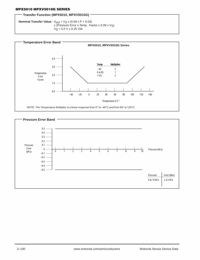
3–100 Motorola Sensor Device Datawww.motorola.com/semiconductors
Transfer Function (MPX5010, MPXV5010G)
Nominal Transfer Value: Vout = VS x (0.09 x P + 0.04)Nominal Transfer Value: ± (Pressure Error x Temp. Factor x 0.09 x VS)Nominal Transfer Value: VS = 5.0 V ± 0.25 Vdc
Temperature Error Band
Temp Multiplier
– 40 30 to 85 1+125 3
Temperature in C°
4.0
3.0
2.0
0.0
1.0
–40 –20 0 20 40 60 14012010080
MPX5010, MPXV5010G Series
TemperatureError
Factor
Pressure Error Band
NOTE: The Temperature Multiplier is a linear response from 0° to –40°C and from 85° to 125°C.
Pressure (kPa)
0.5
0.4
0.2
–0.3
–0.4
–0.5
01 2 3 4 5 6 7
Pressure Error (Max)
0 to 10 kPa ± 0.5 kPa
8 90
0.3
0.1
–0.2
–0.110
PressureError(kPa)

3–101Motorola Sensor Device Data www.motorola.com/semiconductors
PRESSURE (P1)/VACUUM (P2) SIDE IDENTIFICATION TABLE
Motorola designates the two sides of the pressure sensoras the Pressure (P1) side and the Vacuum (P2) side. ThePressure (P1) side is the side containing fluoro silicone gelwhich protects the die from harsh media. The Motorola MPX
pressure sensor is designed to operate with positive differen-tial pressure applied, P1 > P2.
The Pressure (P1) side may be identified by using the tablebelow:
Part Number Case TypePressure (P1)Side Identifier
MPX5010D 867C Stainless Steel Cap
MPX5010DP 867C Side with Part Marking
MPX5010GP 867B Side with Port Attached
MPX5010GS 867E Side with Port Attached
MPX5010GSX 867F Side with Port Attached
MPXV5010G6U 482 Stainless Steel Cap
MPXV5010G7U 482B Stainless Steel Cap
MPXV5010GC6U/T1 482A Side with Port Attached
MPXV5010GC7U 482C Side with Port Attached
MPXV5010GP 1369 Side with Port Attached
MPXV5010DP 1351 Side with Part Marking
ORDERING INFORMATION — UNIBODY PACKAGE (MPX5010 SERIES)
MPX Series
Device Type Options Case Type Order Number Device Marking
Basic Element Differential 867 MPX5010D MPX5010D
Ported Elements Differential, Dual Port 867C MPX5010DP MPX5010DP
Gauge 867B MPX5010GP MPX5010GP
Gauge, Axial 867E MPX5010GS MPX5010D
Gauge, Axial PC Mount 867F MPX5010GSX MPX5010D
ORDERING INFORMATION — SMALL OUTLINE PACKAGE (MPXV5010G SERIES)
Device Type Options Case No. MPX Series Order No. Packing Options Marking
Basic Elements Gauge, Element Only, SMT 482 MPXV5010G6U Rails MPXV5010G
Gauge, Element Only, DIP 482B MPXV5010G7U Rails MPXV5010G
Ported Elements Gauge, Axial Port, SMT 482A MPXV5010GC6U Rails MPXV5010G
Gauge, Axial Port, DIP 482C MPXV5010GC7U Rails MPXV5010G
Gauge, Axial Port, SMT 482A MPXV5010GC6T1 Tape and Reel MPXV5010G
Gauge, Side Port, SMT 1369 MPXV5010GP Trays MPXV5010G
Differential, Dual Port, SMT 1351 MPXV5010DP Trays MPXV5010G
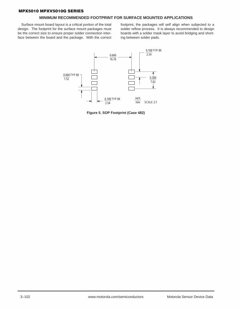
3–102 Motorola Sensor Device Datawww.motorola.com/semiconductors
MINIMUM RECOMMENDED FOOTPRINT FOR SURFACE MOUNTED APPLICATIONS
Surface mount board layout is a critical portion of the totaldesign. The footprint for the surface mount packages mustbe the correct size to ensure proper solder connection inter-face between the board and the package. With the correct
footprint, the packages will self align when subjected to asolder reflow process. It is always recommended to designboards with a solder mask layer to avoid bridging and short-ing between solder pads.
0.66016.76
0.060 TYP 8X1.52
0.100 TYP 8X2.54
0.100 TYP 8X2.54
0.3007.62
Figure 5. SOP Footprint (Case 482)
inchmm SCALE 2:1
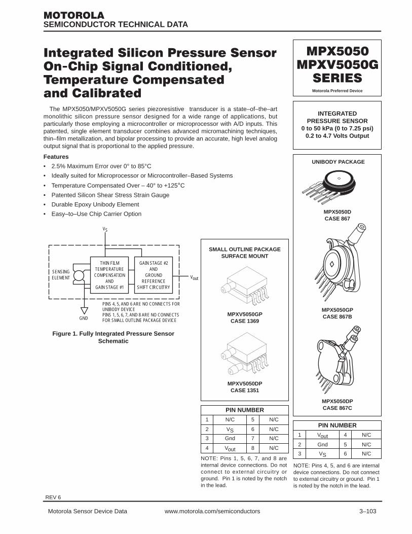
3–103Motorola Sensor Device Data www.motorola.com/semiconductors
#!# !""$! "! # !#$! "# !#
The MPX5050/MPXV5050G series piezoresistive transducer is a state–of–the–artmonolithic silicon pressure sensor designed for a wide range of applications, butparticularly those employing a microcontroller or microprocessor with A/D inputs. Thispatented, single element transducer combines advanced micromachining techniques,thin–film metallization, and bipolar processing to provide an accurate, high level analogoutput signal that is proportional to the applied pressure.
Features
• 2.5% Maximum Error over 0° to 85°C• Ideally suited for Microprocessor or Microcontroller–Based Systems
• Temperature Compensated Over – 40° to +125°C
• Patented Silicon Shear Stress Strain Gauge
• Durable Epoxy Unibody Element
• Easy–to–Use Chip Carrier Option
Figure 1. Fully Integrated Pressure SensorSchematic
VS
SENSINGELEMENT
GND
THIN FILMTEMPERATURECOMPENSATION
ANDGAIN STAGE #1
GAIN STAGE #2AND
GROUNDREFERENCE
SHIFT CIRCUITRY
Vout
PINS 4, 5, AND 6 ARE NO CONNECTS FORUNIBODY DEVICEPINS 1, 5, 6, 7, AND 8 ARE NO CONNECTSFOR SMALL OUTLINE PACKAGE DEVICE
SEMICONDUCTOR TECHNICAL DATA
INTEGRATEDPRESSURE SENSOR
0 to 50 kPa (0 to 7.25 psi)0.2 to 4.7 Volts Output
PIN NUMBER
NOTE: Pins 4, 5, and 6 are internaldevice connections. Do not connectto external circuitry or ground. Pin 1is noted by the notch in the lead.
MPX5050DCASE 867
MPX5050DPCASE 867C
1
2
3
Vout
Gnd
VS
4
5
6
N/C
N/C
N/C
MPX5050GPCASE 867B
UNIBODY PACKAGE
SMALL OUTLINE PACKAGESURFACE MOUNT
MPXV5050DPCASE 1351
MPXV5050GPCASE 1369
PIN NUMBER
1
2
3
N/C
VSGnd
5
6
7
N/C
N/C
N/C
4 Vout 8 N/C
NOTE: Pins 1, 5, 6, 7, and 8 areinternal device connections. Do notconnect to external circuitry orground. Pin 1 is noted by the notchin the lead.
Motorola Preferred Device
REV 6

3–104 Motorola Sensor Device Datawww.motorola.com/semiconductors
MAXIMUM RATINGS(NOTE)
Parametrics Symbol Value Unit
Maximum Pressure (P1 > P2) Pmax 200 kPa
Storage Temperature Tstg –40° to +125° °C
Operating Temperature TA –40° to +125° °C
NOTE: Exposure beyond the specified limits may cause permanent damage or degradation to the device.
OPERATING CHARACTERISTICS (VS = 5.0 Vdc, TA = 25°C unless otherwise noted, P1 > P2. Decoupling circuit shown in Figure 4required to meet electrical specifications.)
Characteristic Symbol Min Typ Max Unit
Pressure Range(1) POP 0 — 50 kPa
Supply Voltage(2) VS 4.75 5.0 5.25 Vdc
Supply Current Io — 7.0 10.0 mAdc
Minimum Pressure Offset(3) (0 to 85°C)@ VS = 5.0 Volts
Voff 0.088 0.20 0.313 Vdc
Full Scale Output(4) (0 to 85°C)@ VS = 5.0 Volts
VFSO 4.587 4.70 4.813 Vdc
Full Scale Span(5) (0 to 85°C)@ VS = 5.0 Volts
VFSS — 4.50 — Vdc
Accuracy(6) — — — 2.5 %VFSS
Sensitivity V/P — 90 — mV/kPa
Response Time(7) tR — 1.0 — ms
Output Source Current at Full Scale Output Io+ — 0.1 — mAdc
Warm–Up Time(8) — — 20 — ms
Offset Stability(9) — — 0.5 — %VFSS
NOTES:1. 1.0kPa (kiloPascal) equals 0.145 psi.2. Device is ratiometric within this specified excitation range.3. Offset (Voff) is defined as the output voltage at the minimum rated pressure.4. Full Scale Output (VFSO) is defined as the output voltage at the maximum or full rated pressure.5. Full Scale Span (VFSS) is defined as the algebraic difference between the output voltage at full rated pressure and the output voltage at the
minimum rated pressure.6. Accuracy (error budget) consists of the following:
• Linearity: Output deviation from a straight line relationship with pressure over the specified pressure range.• Temperature Hysteresis: Output deviation at any temperature within the operating temperature range, after the temperature is
cycled to and from the minimum or maximum operating temperature points, with zero differential pressureapplied.
• Pressure Hysteresis: Output deviation at any pressure within the specified range, when this pressure is cycled to and fromminimum or maximum rated pressure at 25°C.
• TcSpan: Output deviation over the temperature range of 0° to 85°C, relative to 25°C.• TcOffset: Output deviation with minimum pressure applied, over the temperature range of 0° to 85°C, relative
to 25°C.• Variation from Nominal: The variation from nominal values, for Offset or Full Scale Span, as a percent of VFSS at 25°C.
7. Response Time is defined as the time for the incremental change in the output to go from 10% to 90% of its final value when subjected toa specified step change in pressure.
8. Warm–up Time is defined as the time required for the product to meet the specified output voltage after the Pressure has been stabilized.9. Offset Stability is the product’s output deviation when subjected to 1000 hours of Pulsed Pressure, Temperature Cycling with Bias Test.
MECHANICAL CHARACTERISTICS
Characteristics Typ Unit
Weight, Basic Element (Case 867) 4.0 grams
Weight, Basic Element (Case 1369) 1.5 grams

3–105Motorola Sensor Device Data www.motorola.com/semiconductors
Figure 3 illustrates the Differential/Gauge Sensing Chip inthe basic chip carrier (Case 867). A fluorosilicone gel isolatesthe die surface and wire bonds from the environment, whileallowing the pressure signal to be transmitted to the sensordiaphragm.
The MPX5050/MPXV5050G series pressure sensor oper-ating characteristics, and internal reliability and qualificationtests are based on use of dry air as the pressure media. Me-dia, other than dry air, may have adverse effects on sensorperformance and long–term reliability. Contact the factory for
information regarding media compatibility in your application.Figure 2 shows the sensor output signal relative to pres-
sure input. Typical, minimum, and maximum output curvesare shown for operation over a temperature range of 0° to85°C using the decoupling circuit shown in Figure 4. Theoutput will saturate outside of the specified pressure range.
Figure 4 shows the recommended decoupling circuit forinterfacing the output of the integrated sensor to the A/D in-put of a microprocessor or microcontroller. Proper decoup-ling of the power supply is recommended.
Figure 2. Output versus Pressure Differential
MAX
DIFFERENTIAL PRESSURE (kPa)
5.0
4.0
3.0
2.0
05535150
OU
TPU
T (V
)
4525
4.5
3.5
2.5
1.5
5
TRANSFER FUNCTION: Vout = VS*(0.018*P+0.04) ± ERRORVS = 5.0 VdcTEMP = 0 to 85°C
1.0
0.5
503010 4020
MIN
TYPICAL
Figure 3. Cross–Sectional Diagram(Not to Scale)
ÉÉÉÉÉÉÉÉÉÉÉÉÉÉÉÉÉÉÉÉÉÉÉÉÉÉÉÉÉÉÉÉÉÉÉÉÉÉÉÉÉÉÉÉ
FLUORO SILICONEGEL DIE COAT
WIRE BOND
LEAD FRAME
DIE STAINLESS STEELMETAL COVER
EPOXYPLASTIC
CASE
DIFFERENTIAL/GAUGE ELEMENT
DIEBOND
P1
P2
Figure 4. Recommended power supply decouplingand output filtering.
For additional output filtering, please refer toApplication Note AN1646.
1.0 F
IPS
470 pF
OUTPUT
Vs
5 V
0.01 F GND
Vout

3–106 Motorola Sensor Device Datawww.motorola.com/semiconductors
Nominal Transfer Value: Vout = VS (P x 0.018 + 0.04)+/– (Pressure Error x Temp. Factor x 0.018 x VS)VS = 5.0 V ± 0.25 Vdc
Transfer Function
0.0–40 –20 0 20 40 60 14012010080
Temperature Error Band
– 40 30 to 85 1+125 3
Temperature in °C
4.0
3.0
2.0
1.0
MPX5050/MPXV5050G Series
Temp Multiplier
TemperatureError
Factor
NOTE: The Temperature Multiplier is a linear response from 0° to –40°C and from 85° to 125°C.
Pressure Error Band
Error Limits for Pressure
Pressure (in kPa)
3.0
2.0
1.0
–1.0
– 2.0
– 3.0
0.00 10 20 30 40 50 60
Pres
sure
Erro
r (kP
a)
Pressure Error (Max)
0 to 50 kPa ± 1.25 kPa
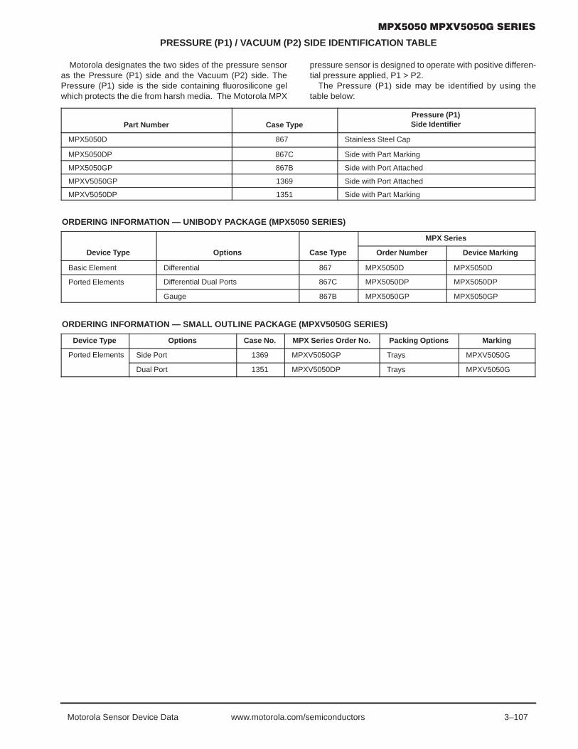
3–107Motorola Sensor Device Data www.motorola.com/semiconductors
PRESSURE (P1) / VACUUM (P2) SIDE IDENTIFICATION TABLE
Motorola designates the two sides of the pressure sensoras the Pressure (P1) side and the Vacuum (P2) side. ThePressure (P1) side is the side containing fluorosilicone gelwhich protects the die from harsh media. The Motorola MPX
pressure sensor is designed to operate with positive differen-tial pressure applied, P1 > P2.
The Pressure (P1) side may be identified by using thetable below:
Part Number Case TypePressure (P1)Side Identifier
MPX5050D 867 Stainless Steel Cap
MPX5050DP 867C Side with Part Marking
MPX5050GP 867B Side with Port Attached
MPXV5050GP 1369 Side with Port Attached
MPXV5050DP 1351 Side with Part Marking
ORDERING INFORMATION — UNIBODY PACKAGE (MPX5050 SERIES)
MPX Series
Device Type Options Case Type Order Number Device Marking
Basic Element Differential 867 MPX5050D MPX5050D
Ported Elements Differential Dual Ports 867C MPX5050DP MPX5050DP
Gauge 867B MPX5050GP MPX5050GP
ORDERING INFORMATION — SMALL OUTLINE PACKAGE (MPXV5050G SERIES)
Device Type Options Case No. MPX Series Order No. Packing Options Marking
Ported Elements Side Port 1369 MPXV5050GP Trays MPXV5050G
Dual Port 1351 MPXV5050DP Trays MPXV5050G

3–108 Motorola Sensor Device Datawww.motorola.com/semiconductors
" " !!# ! " "# !" "
The MPX5100 series piezoresistive transducer is a state–of–the–art monolithic siliconpressure sensor designed for a wide range of applications, but particularly thoseemploying a microcontroller or microprocessor with A/D inputs. This patented, singleelement transducer combines advanced micromachining techniques, thin–film metalliza-tion, and bipolar processing to provide an accurate, high level analog output signal that isproportional to the applied pressure.
Features
• 2.5% Maximum Error over 0° to 85°C• Ideally suited for Microprocessor or Microcontroller–Based Systems
• Patented Silicon Shear Stress Strain Gauge
• Available in Absolute, Differential and Gauge Configurations
• Durable Epoxy Unibody Element
• Easy–to–Use Chip Carrier Option
VS
SENSINGELEMENT
GND
THIN FILMTEMPERATURECOMPENSATION
ANDGAIN STAGE #1
GAIN STAGE #2AND
GROUNDREFERENCE
SHIFT CIRCUITRY
PINS 4, 5 AND 6 ARE NO CONNECTS
Figure 1. Fully Integrated Pressure Sensor Schematic
Vout
SEMICONDUCTOR TECHNICAL DATA
INTEGRATED PRESSURESENSOR
0 to 100 kPa (0 to 14.5 psi)15 to 115 kPa
(2.18 to 16.68 psi)0.2 to 4.7 Volts Output
PIN NUMBER
NOTE: Pins 4, 5, and 6 are internaldevice connections. Do not connectto external circuitry or ground. Pin 1is noted by the notch in the lead.
MPX5100DCASE 867
MPX5100DPCASE 867C
1
2
3
Vout
Gnd
VS
4
5
6
N/C
N/C
N/C
MPX5100GSXCASE 867F
REV 7

3–109Motorola Sensor Device Data www.motorola.com/semiconductors
MAXIMUM RATINGS(NOTE)
Parametrics Symbol Value Unit
Maximum Pressure (P1 > P2) Pmax 400 kPa
Storage Temperature Tstg –40° to +125° °C
Operating Temperature TA – 40° to +125° °C
NOTE: Exposure beyond the specified limits may cause permanent damage or degradation to the device.
OPERATING CHARACTERISTICS (VS = 5.0 Vdc, TA = 25°C unless otherwise noted, P1 > P2. Decoupling circuit shown in Figure 4required to meet electrical specifications.)
Characteristic Symbol Min Typ Max Unit
Pressure Range(1) Gauge, Differential: MPX5100DAbsolute: MPX5100A
POP 015
——
100115
kPa
Supply Voltage(2) VS 4.75 5.0 5.25 Vdc
Supply Current Io — 7.0 10 mAdc
Minimum Pressure Offset(3) (0 to 85°C)@ VS = 5.0 Volts
Voff 0.088 0.20 0.313 Vdc
Full Scale Output(4) Differential and Absolute (0 to 85°C)@ VS = 5.0 Volts Vacuum(10)
VFSO 4.5873.688
4.7003.800
4.8133.913
Vdc
Full Scale Span(5) Differential and Absolute (0 to 85°C)@ VS = 5.0 Volts Vacuum(10)
VFSS ——
4.5003.600
——
Vdc
Accuracy(6) — — — 2.5 %VFSS
Sensitivity V/P — 45 — mV/kPa
Response Time(7) tR — 1.0 — ms
Output Source Current at Full Scale Output Io+ — 0.1 — mAdc
Warm–Up Time(8) — — 20 — ms
Offset Stability(9) — — 0.5 — %VFSS
NOTES:1. 1.0kPa (kiloPascal) equals 0.145 psi.2. Device is ratiometric within this specified excitation range.3. Offset (Voff) is defined as the output voltage at the minimum rated pressure.4. Full Scale Output (VFSO) is defined as the output voltage at the maximum or full rated pressure.5. Full Scale Span (VFSS) is defined as the algebraic difference between the output voltage at full rated pressure and the output voltage at the
minimum rated pressure.6. Accuracy (error budget) consists of the following:
• Linearity: Output deviation from a straight line relationship with pressure over the specified pressure range.• Temperature Hysteresis: Output deviation at any temperature within the operating temperature range, after the temperature is
cycled to and from the minimum or maximum operating temperature points, with zero differential pressureapplied.
• Pressure Hysteresis: Output deviation at any pressure within the specified range, when this pressure is cycled to and from minimum or maximum rated pressure at 25°C.
• TcSpan: Output deviation over the temperature range of 0° to 85°C, relative to 25°C.• TcOffset: Output deviation with minimum pressure applied, over the temperature range of 0° to 85°C, relative
to 25°C.• Variation from Nominal: The variation from nominal values, for Offset or Full Scale Span, as a percent of VFSS at 25°C.
7. Response Time is defined as the time for the incremental change in the output to go from 10% to 90% of its final value when subjected toa specified step change in pressure.
8. Warm–up Time is defined as the time required for the product to meet the specified output voltage after the Pressure has been stabilized.9. Offset Stability is the product’s output deviation when subjected to 1000 hours of Pulsed Pressure, Temperature Cycling with Bias Test.
MECHANICAL CHARACTERISTICS
Characteristics Typ Unit
Weight, Basic Element (Case 867) 4.0 grams

3–110 Motorola Sensor Device Datawww.motorola.com/semiconductors
ON–CHIP TEMPERATURE COMPENSATION, CALIBRATION and SIGNAL CONDITIONING
Figure 2. Output versus Pressure Differential
Figure 2 shows the sensor output signal relative topressure input. Typical, minimum, and maximum out-put curves are shown for operation over a temperaturerange of 0° to 85°C using the decoupling circuit shownin Figure 4. The output will saturate outside of the spe-cified pressure range.
OU
TPU
T (V
)
5
4.5
4
3.5
3
PRESSURE (kPa)
TYP
MAX
MIN
0 10 20 30 40 50 60 70 80 90 100
2.5
2
1.5
1
0.5
0
110
VS = 5 VdcTA = 25°CMPX5100
SPAN
RAN
GE
(TYP
)
OU
TPU
T R
ANG
E (T
YP)
OFFSET(TYP)
ÉÉÉÉÉÉÉÉÉÉÉÉÉÉÉÉÉÉÉÉÉÉÉÉÉÉÉÉÉÉÉÉÉÉÉÉÉÉÉÉÉÉÉÉÉÉÉÉÉÉÉÉÉÉÉ
FLUORO SILICONEGEL DIE COAT
WIRE BOND
LEAD FRAME
DIE STAINLESS STEELMETAL COVER
EPOXY PLASTICCASE
DIFFERENTIAL/GAUGE ELEMENT
DIEBOND
ÉÉÉÉÉÉÉÉÉÉÉÉÉÉÉÉÉÉÉÉÉÉÉÉÉÉÉÉÉÉÉÉÉÉÉÉÉÉÉÉÉÉÉÉÉÉÉÉÉÉÉÉÉÉÉ
FLUORO SILICONEGEL DIE COAT
WIRE BOND
LEAD FRAME
DIESTAINLESS STEEL
METAL COVEREPOXY PLASTIC
CASE
DIEBONDABSOLUTE ELEMENT
Figure 3. Cross–Sectional Diagrams(Not to Scale)
Figure 3 illustrates both the Differential/Gauge and theAbsolute Sensing Chip in the basic chip carrier (Case 867).A fluorosilicone gel isolates the die surface and wire bondsfrom the environment, while allowing the pressure signal tobe transmitted to the sensor diaphragm.
The MPX5100 series pressure sensor operating char-acteristics, and internal reliability and qualification testsare based on use of dry air as the pressure media. Media,
other than dry air, may have adverse effects on sensorperformance and long–term reliability. Contact the fac-tory for information regarding media compatibility in yourapplication.
Figure 4 shows the recommended decoupling circuit forinterfacing the output of the integrated sensor to the A/D in-put of a microprocessor or microcontroller. Proper decoup-ling of the power supply is recommended.
Figure 4. Recommended power supply decouplingand output filtering.
For additional output filtering, please refer toApplication Note AN1646.
1.0 F
IPS
470 pF
OUTPUT
Vs
5 V
0.01 F GND
Vout

3–111Motorola Sensor Device Data www.motorola.com/semiconductors
Nominal Transfer Value: Vout = VS (P x 0.009 + 0.04)+/– (Pressure Error x Temp. Mult. x 0.009 x VS)VS = 5.0 V ±5% P kPa
Transfer Function (MPX5100D, MPX5100G)
Temperature Error Multiplier
Break Points
Temp Multiplier
Temperature in °C
4.0
3.0
2.0
0.0
1.0
–40 –20 0 20 40 60 13012010080
MPX5100D Series
Pressure Error Band
Pressure in kPa
3.0
2.0
1.0
–1.0
–2.0
–3.0
0.00 20 40 60 80 100 120
Pressure Error (max)
0 to 100 kPa ± 2.5 kPa
– 40 30 to 85 1+125 3
NOTE: The Temperature Multiplier is a linear response from 0° to –40°C and from 85° to 125°C.
140
Erro
r (kP
a)
Error Limits for Pressure
MPX5100D Series

3–112 Motorola Sensor Device Datawww.motorola.com/semiconductors
Nominal Transfer Value: Vout = VS (P x 0.009 – 0.095)+/– (Pressure Error x Temp. Mult. x 0.009 x VS)VS = 5.0 V ±5% P kPa
Transfer Function (MPX5100A)
Temperature Error Multiplier
Break Points
Temp Multiplier
Temperature in °C
4.0
3.0
2.0
0.0
1.0
–40 –20 0 20 40 60 13012010080
MPX5100A Series
Pressure Error Band
– 40 30 to 85 1+125 3
140
NOTE: The Temperature Multiplier is a linear response from 0° to –40°C and from 85° to 125°C.
Pressure in kPa
3.0
2.0
1.0
–1.0
–2.0
–3.0
0.00 20 40 60 80 100 130
Pressure Error (max)
15 to 115 kPa ± 2.5 kPa
Erro
r (kP
a)
Error Limits for Pressure
MPX5100A Series

3–113Motorola Sensor Device Data www.motorola.com/semiconductors
PRESSURE (P1)/VACUUM (P2) SIDE IDENTIFICATION TABLE
Motorola designates the two sides of the pressure sensoras the Pressure (P1) side and the Vacuum (P2) side. ThePressure (P1) side is the side containing fluoro silicone gelwhich protects the die from harsh media. The Motorola MPX
pressure sensor is designed to operate with positive differen-tial pressure applied, P1 > P2.
The Pressure (P1) side may be identified by using theTable below:
Part Number Case TypePressure (P1)Side Identifier
MPX5100A, MPX5100D 867 Stainless Steel Cap
MPX5100DP 867C Side with Part Marking
MPX5100AP, MPX5100GP 867B Side with Port Attached
MPX5100GSX 867F Side with Port Attached
ORDERING INFORMATION:
The MPX5100 pressure sensor is available in absolute, differential, and gauge configurations. Devices are available in thebasic element package or with pressure port fittings that provide printed circuit board mounting ease and barbed hose pres-sure connections.
MPX Series
Device Name Options Case Type Order Number Device Marking
Basic Element Absolute 867 MPX5100A MPX5100A
Differential 867 MPX5100D MPX5100D
Ported Elements Differential Dual Ports 867C MPX5100DP MPX5100DP
Absolute, Single Port 867B MPX5100AP MPX5100AP
Gauge, Single Port 867B MPX5100GP MPX5100GP
Gauge, Axial PC Mount 867F MPX5100GSX MPX5100D
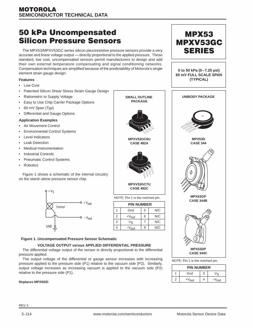
3–114 Motorola Sensor Device Datawww.motorola.com/semiconductors
! "
The MPX53/MPXV53GC series silicon piezoresistive pressure sensors provide a veryaccurate and linear voltage output — directly proportional to the applied pressure. Thesestandard, low cost, uncompensated sensors permit manufacturers to design and addtheir own external temperature compensating and signal conditioning networks.Compensation techniques are simplified because of the predictability of Motorola’s singleelement strain gauge design.
Features
• Low Cost
• Patented Silicon Shear Stress Strain Gauge Design
• Ratiometric to Supply Voltage
• Easy to Use Chip Carrier Package Options
• 60 mV Span (Typ)
• Differential and Gauge Options
Application Examples
• Air Movement Control
• Environmental Control Systems
• Level Indicators
• Leak Detection
• Medical Instrumentation
• Industrial Controls
• Pneumatic Control Systems
• Robotics
Figure 1 shows a schematic of the internal circuitryon the stand–alone pressure sensor chip.
VOLTAGE OUTPUT versus APPLIED DIFFERENTIAL PRESSUREThe differential voltage output of the sensor is directly proportional to the differential
pressure applied.The output voltage of the differential or gauge sensor increases with increasing
pressure applied to the pressure side (P1) relative to the vacuum side (P2). Similarly,output voltage increases as increasing vacuum is applied to the vacuum side (P2)relative to the pressure side (P1).
Replaces MPX50/D
SEMICONDUCTOR TECHNICAL DATA
MPX53DCASE 344
MPX53GPCASE 344B
0 to 50 kPa (0–7.25 psi)60 mV FULL SCALE SPAN
(TYPICAL)
NOTE: Pin 1 is the notched pin.
PIN NUMBER
1
2
Gnd
+Vout
3
4
VS
–Vout
SMALL OUTLINE PACKAGE
MPXV53GC6UCASE 482A
MPXV53GC7UCASE 482C
PIN NUMBER
1
2
3
Gnd
+VoutVS
5
6
7
N/C
N/C
N/C
4 –Vout 8 N/C
UNIBODY PACKAGE
NOTE: Pin 1 is the notched pin.
MPX53DPCASE 344C
Figure 1. Uncompensated Pressure Sensor Schematic
Sensor+ Vout
– Vout
+ VS
GND
REV 2

3–115Motorola Sensor Device Data www.motorola.com/semiconductors
MAXIMUM RATINGS(NOTE)
Rating Symbol Value Unit
Maximum Pressure (P1 > P2) Pmax 200 kPa
Storage Temperature Tstg –40 to +125 °C
Operating Temperature TA –40 to +125 °C
NOTE: Exposure beyond the specified limits may cause permanent damage or degradation to the device.
OPERATING CHARACTERISTICS (VS = 3.0 Vdc, TA = 25°C unless otherwise noted, P1 > P2)
Characteristic Symbol Min Typ Max Unit
Pressure Range(1) POP 0 — 50 kPa
Supply Voltage(2) VS — 3.0 6.0 Vdc
Supply Current Io — 6.0 — mAdc
Full Scale Span(3) VFSS 45 60 90 mV
Offset(4) Voff 0 20 35 mV
Sensitivity ∆V/∆P — 1.2 — mV/kPa
Linearity(5) — –0.6 — 0.4 %VFSS
Pressure Hysteresis(5) (0 to 50 kPa) — — ± 0.1 — %VFSS
Temperature Hysteresis(5) (– 40°C to +125°C) — — ± 0.5 — %VFSS
Temperature Coefficient of Full Scale Span(5) TCVFSS –0.22 — –0.16 %VFSS/°C
Temperature Coefficient of Offset(5) TCVoff — ± 15 — µV/°C
Temperature Coefficient of Resistance(5) TCR 0.31 — 0.37 %Zin/°C
Input Impedance Zin 355 — 505 Ω
Output Impedance Zout 750 — 1875 Ω
Response Time(6) (10% to 90%) tR — 1.0 — ms
Warm–Up — — 20 — ms
Offset Stability(7) — — ± 0.5 — %VFSS
NOTES:1. 1.0 kPa (kiloPascal) equals 0.145 psi.2. Device is ratiometric within this specified excitation range. Operating the device above the specified excitation range may induce additional
error due to device self–heating.3. Full Scale Span (VFSS) is defined as the algebraic difference between the output voltage at full rated pressure and the output voltage at the
minimum rated pressure.4. Offset (Voff) is defined as the output voltage at the minimum rated pressure.5. Accuracy (error budget) consists of the following:
• Linearity: Output deviation from a straight line relationship with pressure, using end point method, over the specified pressure range.
• Temperature Hysteresis: Output deviation at any temperature within the operating temperature range, after the temperature is cycled to and from the minimum or maximum operating temperature points, with zero differential pressure applied.
• Pressure Hysteresis: Output deviation at any pressure within the specified range, when this pressure is cycled to and from the minimum or maximum rated pressure, at 25°C.
• TcSpan: Output deviation at full rated pressure over the temperature range of 0 to 85°C, relative to 25°C.• TcOffset: Output deviation with minimum rated pressure applied, over the temperature range of 0 to 85°C, relative
to 25°C.• TCR: Zin deviation with minimum rated pressure applied, over the temperature range of –40°C to +125°C,
relative to 25°C.6. Response Time is defined as the time for the incremental change in the output to go from 10% to 90% of its final value when subjected to
a specified step change in pressure.7. Offset stability is the product’s output deviation when subjected to 1000 hours of Pulsed Pressure, Temperature Cycling with Bias Test.

3–116 Motorola Sensor Device Datawww.motorola.com/semiconductors
TEMPERATURE COMPENSATIONFigure 2 shows the typical output characteristics of the
MPX53/MPXV53GC series over temperature.The piezoresistive pressure sensor element is a semicon-
ductor device which gives an electrical output signal propor-tional to the pressure applied to the device. This device usesa unique transverse voltage diffused semiconductor straingauge which is sensitive to stresses produced in a thin sili-con diaphragm by the applied pressure.
Because this strain gauge is an integral part of the silicondiaphragm, there are no temperature effects due to differ-ences in the thermal expansion of the strain gauge and thediaphragm, as are often encountered in bonded strain gaugepressure sensors. However, the properties of the straingauge itself are temperature dependent, requiring that thedevice be temperature compensated if it is to be used overan extensive temperature range.
Temperature compensation and offset calibration can beachieved rather simply with additional resistive components,
or by designing your system using the MPX2053 seriessensors.
Several approaches to external temperature compensa-tion over both –40 to +125°C and 0 to +80°C ranges arepresented in Motorola Applications Note AN840.
LINEARITYLinearity refers to how well a transducer’s output follows
the equation: Vout = Voff + sensitivity x P over the operatingpressure range (see Figure 3). There are two basic methodsfor calculating nonlinearity: (1) end point straight line fit or (2)a least squares best line fit. While a least squares fit givesthe “best case” linearity error (lower numerical value), thecalculations required are burdensome.
Conversely, an end point fit will give the “worst case” error(often more desirable in error budget calculations) and thecalculations are more straightforward for the user. Motoro-la’s specified pressure sensor linearities are based on theend point straight line method measured at the midrangepressure.
Figure 2. Output versus Pressure Differential Figure 3. Linearity Specification Comparison
Figure 4. Cross–Sectional Diagram (not to scale)
ÉÉÉÉÉÉÉÉÉÉÉÉÉÉÉÉÉÉÉÉÉÉÉÉÉÉÉÉÉÉÉÉÉÉÉÉÉÉÉÉÉÉÉÉÉÉÉÉÉÉÉÉÉÉÉ
SILICONEDIE COAT
WIRE BOND
LEAD FRAME
DIE STAINLESS STEELMETAL COVER
EPOXYCASE
RTV DIEBOND
P1
P2
100
0 1 2 3 4 5 6 7 810 20 30 40 50
PSIkPa 0
OU
TPU
T (m
Vdc)
PRESSURE DIFFERENTIAL
OFFSET(TYP)
OFFSET(VOFF)
70
OU
TPU
T (m
Vdc)
60
50
40
30
20
10
00 MAX POP
SPAN(VFSS)
PRESSURE (kPA)
ACTUAL
THEORETICAL
LINEARITY90
80
70
60
50
40
30
20
100
SPANRANGE(TYP)
– 40°C
+ 125°C
+ 25°CMPX53VS = 3 Vdc
P1 > P2
Figure 4 illustrates the differential or gauge configurationin the unibody chip carrier (Case 344). A silicone gel isolatesthe die surface and wire bonds from the environment, whileallowing the pressure signal to be transmitted to the silicondiaphragm.
The MPX53/MPXV53GC series pressure sensor operating
characteristics and internal reliability and qualification testsare based on use of dry air as the pressure media. Mediaother than dry air may have adverse effects on sensor perfor-mance and long term reliability. Contact the factory for in-formation regarding media compatibility in your application.

3–117Motorola Sensor Device Data www.motorola.com/semiconductors
PRESSURE (P1)/VACUUM (P2) SIDE IDENTIFICATION TABLE
Motorola designates the two sides of the pressure sensoras the Pressure (P1) side and the Vacuum (P2) side. ThePressure (P1) side is the side containing silicone gel whichisolates the die from the environment. The Motorola pres-
sure sensor is designed to operate with positive differentialpressure applied, P1 > P2.
The Pressure (P1) side may be identified by using thetable below:
Part Number Case Type Pressure (P1) Side Identifier
MPX53D 344 Stainless Steel Cap
MPX53DP 344C Side with Port Marking
MPX53GP 344B Side with Port Attached
MPXV53GC series 482A, 482C Sides with Port Attached
ORDERING INFORMATION – UNIBODY PACKAGE
MPX53 series pressure sensors are available in differential and gauge configurations. Devices are available with basicelement package or with pressure port fittings which provide printed circuit board mounting ease and barbed hose pressureconnections.
MPX Series
Device Type Options Case Type Order Number Device Marking
Basic Element Differential Case 344 MPX53D MPX53D
Ported Elements Differential Case 344C MPX53DP MPX53DP
Gauge Case 344B MPX53GP MPX53GP
ORDERING INFORMATION — SMALL OUTLINE PACKAGE
The MPXV53GC series pressure sensors are available with a pressure port, surface mount or DIP leadforms, and two packingoptions.
Device Order No. Case No. Packing Options Marking
MPXV53GC6T1 482A Tape & Rail MPXV53G
MPXV53GC6U 482A Rails MPXV53G
MPXV53GC7U 482C Rails MPXV53G

3–118 Motorola Sensor Device Datawww.motorola.com/semiconductors
!! " !!" ! !
The MPX5500 series piezoresistive transducer is a state–of–the–art monolithic siliconpressure sensor designed for a wide range of applications, but particularly thoseemploying a microcontroller or microprocessor with A/D inputs. This patented, singleelement transducer combines advanced micromachining techniques, thin–film metalliza-tion, and bipolar processing to provide an accurate, high level analog output signal thatis proportional to the applied pressure.
Features
• 2.5% Maximum Error over 0° to 85°C• Ideally suited for Microprocessor or Microcontroller–Based Systems
• Patented Silicon Shear Stress Strain Gauge
• Durable Epoxy Unibody Element
• Available in Differential and Gauge Configurations
VS
SENSINGELEMENT Vout
GND
THIN FILMTEMPERATURECOMPENSATION
ANDGAIN STAGE #1
GAIN STAGE #2AND
GROUNDREFERENCE
SHIFT CIRCUITRY
PINS 4, 5 AND 6 ARE NO CONNECTS
Figure 1. Fully Integrated Pressure Sensor Schematic
SEMICONDUCTOR TECHNICAL DATA
INTEGRATEDPRESSURE SENSOR
0 to 500 kPa (0 to 72.5 psi)0.2 to 4.7 Volts Output
PIN NUMBER
NOTE: Pins 4, 5, and 6 are internaldevice connections. Do not connectto external circuitry or ground. Pin 1is noted by the notch in the lead.
MPX5500DCASE 867
MPX5500DPCASE 867C
1
2
3
Vout
Gnd
VS
4
5
6
N/C
N/C
N/C
REV 5

3–119Motorola Sensor Device Data www.motorola.com/semiconductors
MAXIMUM RATINGS(1)
Parametrics Symbol Value Unit
Maximum Pressure(2) (P2 1 Atmosphere) P1max 2000 kPa
Storage Temperature Tstg –40° to +125° °C
Operating Temperature TA –40° to +125° °C
NOTES:1. Maximum Ratings apply to Case 867 only. Extended exposure at the specified limits may cause permanent damage or degradation to the
device.2. This sensor is designed for applications where P1 is always greater than, or equal to P2. P2 maximum is 500 kPa.
OPERATING CHARACTERISTICS (VS = 5.0 Vdc, TA = 25°C unless otherwise noted, P1 > P2. Decoupling circuit shown in Figure 4required to meet electrical specifications.)
Characteristic Symbol Min Typ Max Unit
Pressure Range(1) POP 0 — 500 kPa
Supply Voltage(2) VS 4.75 5.0 5.25 Vdc
Supply Current Io — 7.0 10.0 mAdc
Zero Pressure Offset(3) (0 to 85°C) Voff 0.088 0.20 0.313 Vdc
Full Scale Output(4) (0 to 85°C) VFSO 4.587 4.70 4.813 Vdc
Full Scale Span(5) (0 to 85°C) VFSS — 4.50 — Vdc
Accuracy(6) — — — 2.5 %VFSS
Sensitivity V/P — 9.0 — mV/kPa
Response Time(7) tR — 1.0 — ms
Output Source Current at Full Scale Output Io+ — 0.1 — mAdc
Warm–Up Time(8) — — 20 — ms
NOTES:1. 1.0kPa (kiloPascal) equals 0.145 psi.2. Device is ratiometric within this specified excitation range.3. Offset (Voff) is defined as the output voltage at the minimum rated pressure.4. Full Scale Output (VFSO) is defined as the output voltage at full rated pressure.5. Full Scale Span (VFSS) is defined as the algebraic difference between the output voltage at full rated pressure and the output voltage at the
minimum rated pressure.6. Accuracy (error budget) consists of the following:
• Linearity: Output deviation from a straight line relationship with pressure over the specified pressure range.• Temperature Hysteresis: Output deviation at any temperature within the operating temperature range, after the temperature is
cycled to and from the minimum or maximum operating temperature points, with zero differential pressureapplied.
• Pressure Hysteresis: Output deviation at any pressure within the specified range, when this pressure is cycled to and fromminimum or maximum rated pressure at 25°C.
• TcSpan: Output deviation over the temperature range of 0° to 85°C, relative to 25°C.• TcOffset: Output deviation with minimum pressure applied, over the temperature range of 0° to 85°C, relative
to 25°C.• Variation from Nominal: The variation from nominal values, for Offset or Full Scale Span, as a percent of VFSS at 25°C.
7. Response Time is defined as the time for the incremental change in the output to go from 10% to 90% of its final value when subjected toa specified step change in pressure.
8. Warm–up Time is defined as the time required for the device to meet the specified output voltage after the pressure has been stabilized.
MECHANICAL CHARACTERISTICS
Characteristics Typ Unit
Weight, Basic Element (Case 867) 4.0 grams

3–120 Motorola Sensor Device Datawww.motorola.com/semiconductors
Figure 3 illustrates the Differential/Gauge basic chip carrier(Case 867). A fluorosilicone gel isolates the die surface andwire bonds from the environment, while allowing the pres-sure signal to be transmitted to the sensor diaphragm. (Foruse of the MPX5500D in a high pressure, cyclic application,consult the factory.)
The MPX5500 series pressure sensor operating charac-teristics, and internal reliability and qualification tests arebased on use of dry air as the pressure media. Media, otherthan dry air, may have adverse effects on sensor perfor-mance and long–term reliability. Contact the factory for
information regarding media compatibility in your application.Figure 2 shows the sensor output signal relative to pres-
sure input. Typical, minimum, and maximum output curvesare shown for operation over a temperature range of 0° to85°C using the decoupling circuit shown in Figure 4. Theoutput will saturate outside of the specified pressure range.
Figure 4 shows the recommended decoupling circuit forinterfacing the output of the integrated sensor to the A/D in-put of a microprocessor or microcontroller. Proper decoup-ling of the power supply is recommended.
MAX
Figure 2. Output versus Pressure Differential
DIFFERENTIAL PRESSURE (kPa)
5.0
4.0
3.0
2.0
05503501500
OU
TPU
T (V
)
450250
4.5
3.5
2.5
1.5
50
TRANSFER FUNCTION: Vout = VS*(0.0018*P+0.04) ± ERRORVS = 5.0 VdcTEMP = 0 to 85°C
1.0
0.5
500300100 400200
MIN
TYPICAL
ÉÉÉÉÉÉÉÉÉÉÉÉÉÉÉÉÉÉÉÉÉÉÉÉÉÉÉÉÉÉÉÉÉÉÉÉÉÉÉÉÉÉÉÉÉÉÉÉÉÉÉÉÉÉÉÉÉÉÉÉ
FLUORO SILICONEDIE COAT
LEADFRAME
STAINLESS STEELMETAL COVER
RTV DIEBOND
DIE
EPOXY CASE
WIRE BOND
Figure 3. Cross–Sectional Diagram(Not to Scale)
P1
P2
Figure 4. Recommended power supply decouplingand output filtering.
For additional output filtering, please refer toApplication Note AN1646.
1.0 F
IPS
470 pF
OUTPUT
Vs
5 V
0.01 F GND
Vout

3–121Motorola Sensor Device Data www.motorola.com/semiconductors
PRESSURE (P1)/VACUUM (P2) SIDE IDENTIFICATION TABLE
Motorola designates the two sides of the pressure sensoras the Pressure (P1) side and the Vacuum (P2) side. ThePressure (P1) side is the side containing fluorosilicone gelwhich protects the die from the environment. The Motorola
MPX pressure sensor is designed to operate with positive dif-ferential pressure applied, P1 > P2.
The Pressure (P1) side may be identified by using the Tablebelow:
Part Number Case TypePressure (P1)Side Identifier
MPX5500D 867 Stainless Steel Cap
MPX5500DP 867C Side with Part Marking
ORDERING INFORMATION
MPX Series
Device Name Options Case Type Order Number Device Marking
Basic Element Differential 867 MPX5500D MPX5500D
Ported Elements Differential Dual Ports 867C MPX5500DP MPX5500DP

3–122 Motorola Sensor Device Datawww.motorola.com/semiconductors
" " !!# ! " "# !" "
The MPX5700 series piezoresistive transducer is a state–of–the–art monolithic siliconpressure sensor designed for a wide range of applications, but particularly thoseemploying a microcontroller or microprocessor with A/D inputs. This patented, singleelement transducer combines advanced micromachining techniques, thin–film metalliza-tion, and bipolar processing to provide an accurate, high level analog output signal thatis proportional to the applied pressure.
Features
• 2.5% Maximum Error over 0° to 85°C• Ideally Suited for Microprocessor or Microcontroller–Based Systems
• Available in Absolute, Differential and Gauge Configurations
• Patented Silicon Shear Stress Strain Gauge
• Durable Epoxy Unibody Element
Figure 1. Fully Integrated Pressure Sensor Schematic
VS
SENSINGELEMENT Vout
GND
THIN FILMTEMPERATURECOMPENSATION
ANDGAIN STAGE #1
GAIN STAGE #2AND
GROUNDREFERENCE
SHIFT CIRCUITRY
PINS 4, 5 AND 6 ARE NO CONNECTS
SEMICONDUCTOR TECHNICAL DATA
INTEGRATED PRESSURESENSOR
0 to 700 kPa (0 to 101.5 psi)15 to 700 kPa
(2.18 to 101.5 psi)0.2 to 4.7 V OUTPUT
PIN NUMBER
NOTE: Pins 4, 5, and 6 are internaldevice connections. Do not connectto external circuitry or ground. Pin 1is noted by the notch in the lead.
MPX5700DCASE 867
MPX5700DPCASE 867C
1
2
3
Vout
Gnd
VS
4
5
6
N/C
N/C
N/C
MPX5700ASCASE 867E
REV 5

3–123Motorola Sensor Device Data www.motorola.com/semiconductors
MAXIMUM RATINGS(1)
Parametrics Symbol Value Unit
Maximum Pressure(2) (P2 1 Atmosphere) P1max 2800 kPa
Storage Temperature Tstg –40 to +125 °C
Operating Temperature TA –40 to +125 °C
NOTES:1. Maximum Ratings apply to Case 867 only. Extended exposure at the specified limits may cause permanent damage or degradation to the
device.2. This sensor is designed for applications where P1 is always greater than, or equal to P2. P2 maximum is 500 kPa.
OPERATING CHARACTERISTICS (VS = 5.0 Vdc, TA = 25°C unless otherwise noted, P1 > P2. Decoupling circuit shown in Figure 4required to meet electrical specifications.)
Characteristic Symbol Min Typ Max Unit
Pressure Range(1) Gauge, Differential: MPX5700DAbsolute: MPX5700A
POP 015
— 700700
kPa
Supply Voltage(2) VS 4.75 5.0 5.25 Vdc
Supply Current Io – 7.0 10 mAdc
Zero Pressure Offset(3) Gauge, Differential: (0 to 85°C)Absolute (0 to 85°C)
Voff 0.0880.184
0.2 0.3130.409
Vdc
Full Scale Output(4) (0 to 85°C) VFSO 4.587 4.7 4.813 Vdc
Full Scale Span(5) (0 to 85°C) VFSS — 4.5 — Vdc
Accuracy(6) (0 to 85°C) — — — ± 2.5 %VFSS
Sensitivity V/P — 6.4 — mV/kPa
Response Time(7) tR — 1.0 — ms
Output Source Current at Full Scale Output IO+ — 0.1 — mAdc
Warm–Up Time(8) — — 20 — ms
NOTES:1. 1.0 kPa (kiloPascal) equals 0.145 psi.2. Device is ratiometric within this specified excitation range.3. Offset (Voff) is defined as the output voltage at the minimum rated pressure.4. Full Scale Output (VFSO) is defined as the output voltage at the maximum or full rated pressure.5. Full Scale Span (VFSS) is defined as the algebraic difference between the output voltage at full rated pressure and the output voltage at the
minimum rated pressure.6. Accuracy (error budget) consists of the following:
• Linearity: Output deviation from a straight line relationship with pressure over the specified pressure range.• Temperature Hysteresis: Output deviation at any temperature within the operating temperature range, after the temperature is
cycled to and from the minimum or maximum operating temperature points, with zero differential pressureapplied.
• Pressure Hysteresis: Output deviation at any pressure within the specified range, when this pressure is cycled to and from theminimum or maximum rated pressure, at 25°C.
• TcSpan: Output deviation over the temperature range of 0° to 85°C, relative to 25°C.• TcOffset: Output deviation with minimum rated pressure applied, over the temperature range of 0° to 85°C, relative
to 25°C.• Variation from Nominal: The variation from nominal values, for Offset or Full Scale Span, as a percent of VFSS, at 25°C.
7. Response Time is defined as the time for the incremental change in the output to go from 10% to 90% of its final value when subjected toa specified step change in pressure.
8. Warm–up Time is defined as the time required for the device to meet the specified output voltage after the pressure has been stabilized.
MECHANICAL CHARACTERISTICS
Characteristics Typ Unit
Weight, Basic Element (Case 867) 4.0 grams

3–124 Motorola Sensor Device Datawww.motorola.com/semiconductors
ON–CHIP TEMPERATURE COMPENSATION, CALIBRATION AND SIGNAL CONDITIONING
Figure 3 illustrates the Differential/Gauge basic chip car-rier (Case 867). A fluorosilicone gel isolates the die surfaceand wire bonds from the environment, while allowing thepressure signal to be transmitted to the sensor diaphragm.(For use of the MPX5700D in a high pressure, cyclic ap-plication, consult the factory.)
The MPX5700 series pressure sensor operating character-istics, and internal reliability and qualification tests are basedon use of dry air as the pressure media. Media, other than dryair, may have adverse effects on sensor performance andlong–term reliability. Contact the factory for information
regarding media compatibility in your application.Figure 2 shows the sensor output signal relative to pres-
sure input. Typical, minimum, and maximum output curvesare shown for operation over a temperature range of 0° to85°C using the decoupling circuit shown in Figure 4. Theoutput will saturate outside of the specified pressure range.
Figure 4 shows the recommended decoupling circuit forinterfacing the output of the integrated sensor to the A/D in-put of a microprocessor or microcontroller. Proper decoup-ling of the power supply is recommended.
DIFFERENTIAL PRESSURE (kPa)
Figure 2. Output versus Pressure Differential
5.0
4.0
3.0
2.0
07003000 500
4.5
3.5
2.5
1.5
100
1.0
0.5
600200 800400
TYPICAL
OU
TPU
T (V
)
TRANSFER FUNCTION: Vout = VS*(0.0012858*P+0.04) ± ERRORVS = 5.0 VdcTEMP = 0 to 85°C
MAX MIN
ÉÉÉÉÉÉÉÉÉÉÉÉÉÉÉÉÉÉÉÉÉÉÉÉÉÉÉÉÉÉÉÉÉÉÉÉÉÉÉÉÉÉÉÉ
FLUORO SILICONEDIE COAT
LEADFRAME
STAINLESS STEELMETAL COVER
RTV DIEBOND
DIE
EPOXY CASE
WIRE BOND
Figure 3. Cross–Sectional Diagram(Not to Scale)
P1
P2
Figure 4. Recommended power supply decouplingand output filtering.
For additional output filtering, please refer toApplication Note AN1646.
1.0 F
IPS
470 pF
OUTPUT
Vs
5 V
0.01 F GND
Vout

3–125Motorola Sensor Device Data www.motorola.com/semiconductors
PRESSURE (P1)/VACUUM (P2) SIDE IDENTIFICATION TABLE
Motorola designates the two sides of the pressure sensoras the Pressure (P1) side and the Vacuum (P2) side. ThePressure (P1) side is the side containing fluoro silicone gelwhich protects the die from harsh media. The Motorola MPX
pressure sensor is designed to operate with positive differen-tial pressure applied, P1 > P2.
The Pressure (P1) side may be identified by using the tablebelow:
Part Number Case TypePressure (P1)Side Identifier
MPX5700D, MPX5700A 867C Stainless Steel Cap
MPX5700DP 867C Side with Part Marking
MPX5700GP, MPX5700AP 867B Side with Port Attached
MPX5700GS, MPX5700AS 867E Side with Port Attached
ORDERING INFORMATION
MPX Series
Device Type Options Case Type Order Number Device Marking
Basic Element Differential 867C MPX5700D MPX5700D
Absolute 867C MPX5700A MPX5700A
Ported Elements Differential Dual Ports 867C MPX5700DP MPX5700DP
Gauge 867B MPX5700GP MPX5700GP
Gauge, Axial 867E MPX5700GS MPX5700D
Absolute 867B MPX5700AP MPX5700AP
Absolute, Axial 867E MPX5700AS MPX5700A

3–126 Motorola Sensor Device Datawww.motorola.com/semiconductors
!! " !!" ! !
The MPX5999D piezoresistive transducer is a state–of–the–art pressure sensordesigned for a wide range of applications, but particularly for those employing amicrocontroller or microprocessor with A/D inputs. This patented, single elementtransducer combines advanced micromachining techniques, thin–film metallization andbipolar semiconductor processing to provide an accurate, high level analog output signalthat is proportional to applied pressure.
Figure 1 shows a block diagram of the internal circuitry integrated on the stand–alonesensing chip.
Features
• Temperature Compensated Over 0 to 85°C• Ideally Suited for Microprocessor or Microcontroller–Based Systems
• Patented Silicon Shear Stress Strain Gauge
• Durable Epoxy Unibody Element
Figure 1. Fully Integrated Pressure Sensor Schematic
VS
SENSINGELEMENT
Vout
GND
THIN FILMTEMPERATURECOMPENSATION
ANDGAIN STAGE #1
GAIN STAGE #2AND
GROUNDREFERENCE
SHIFT CIRCUITRY
PINS 4, 5 AND 6 ARE NO CONNECTS
SEMICONDUCTOR TECHNICAL DATA
INTEGRATED PRESSURESENSOR
0 to 1000 kPa (0 to 150 psi)0.2 to 4.7 V OUTPUT
PIN NUMBER
1
2
3
Vout
Gnd
VS
4
5
6
N/C
N/C
N/C
MPX5999DCASE 867
NOTE: Pins 4, 5, and 6 are internaldevice connections. Do not connectto external circuitry or ground. Pin 1is noted by the notch in the lead.
REV 4

3–127Motorola Sensor Device Data www.motorola.com/semiconductors
MAXIMUM RATINGS(1)
Parametrics Symbol Value Unit
Maximum Pressure(2) (P1 > P2) P1max 4000 kPa
Storage Temperature Tstg –40° to +125 °C
Operating Temperature TA –40° to +125 °C
NOTES:1. Extended exposure at the specified limits may cause permanent damage or degradation to the device.2. This sensor is designed for applications where P1 is always greater than, or equal to P2. P2 maximum is 500 kPa.
OPERATING CHARACTERISTICS (VS = 5.0 Vdc, TA = 25°C unless otherwise noted, P1 > P2. Decoupling circuit shown in Figure 4required to meet electrical specifications.)
Characteristic Symbol Min Typ Max Unit
Pressure Range(1) POP 0 — 1000 kPa
Supply Voltage(2) VS 4.75 5.0 5.25 Vdc
Supply Current Io — 7.0 10 mAdc
Zero Pressure Offset(3) (0 to 85°C) Voff 0.088 0.2 0.313 Vdc
Full Scale Output(4) (0 to 85°C) VFSO 4.587 4.7 4.813 Vdc
Full Scale Span(5) (0 to 85°C) VFSS — 4.5 — Vdc
Sensitivity V/P — 4.5 — mV/kPa
Accuracy(6) (0 to 85°C) — — — ± 2.5 %VFSS
Response Time(7) tR — 1.0 — ms
Output Source Current at Full Scale Output IO+ — 0.1 — mA
Warm–Up Time(8) — — 20 — ms
NOTES:1. 1.0 kPa (kiloPascal) equals 0.145 psi.2. Device is ratiometric within this specified excitation range.3. Offset (Voff) is defined as the output voltage at the minimum rated pressure.4. Full Scale Output (VFSO) is defined as the output voltage at the maximum or full rated pressure.5. Full Scale Span (VFSS) is defined as the algebraic difference between the output voltage at full rated pressure and the output voltage at the
minimum rated pressure.6. Accuracy (error budget) consists of the following:
• Linearity: Output deviation from a straight line relationship with pressure over the specified pressure range.• Temperature Hysteresis: Output deviation at any temperature within the operating temperature range, after the temperature is
cycled to and from the minimum or maximum operating temperature points, with zero differential pressureapplied.
• Pressure Hysteresis: Output deviation at any pressure within the specified range, when this pressure is cycled to and from theminimum or maximum rated pressure, at 25°C.
• TcSpan: Output deviation over the temperature range of 0° to 85°C, relative to 25°C.• TcOffset: Output deviation with minimum rated pressure applied, over the temperature range of 0° to 85°C, relative
to 25°C.• Variation from Nominal: The variation from nominal values, for Offset or Full Scale Span, as a percent of VFSS, at 25°C.
7. Response Time is defined as the time for the incremental change in the output to go from 10% to 90% of its final value when subjected toa specified step change in pressure.
8. Warm–up Time is defined as the time required for the device to meet the specified output voltage after the pressure has been stabilized.
MECHANICAL CHARACTERISTICS
Characteristics Typ Unit
Weight, Basic Element (Case 867) 4.0 grams

3–128 Motorola Sensor Device Datawww.motorola.com/semiconductors
ON–CHIP TEMPERATURE COMPENSATION, CALIBRATION AND SIGNAL CONDITIONING
Figure 2 shows the sensor output signal relative to pres-sure input. Typical, minimum, and maximum output curvesare shown for operation over a temperature range of 0° to85°C using the decoupling circuit shown in Figure 4. Theoutput will saturate outside of the specified pressure range.
The performance over temperature is achieved by integrat-ing the shear–stress strain gauge, temperature compensa-tion, calibration and signal conditioning circuitry onto a singlemonolithic chip.
Figure 3 illustrates the differential or gauge configuration in thebasic chip carrier (Case 867). A fluoro silicone gel isolates thedie surface and wire bonds from harsh environments, while al-
lowing the pressure signal to be transmitted to the silicon dia-phragm.
The MPX5999D pressure sensor operating characteristics,and internal reliability and qualification tests are based on useof dry air as the pressure media. Media other than dry air mayhave adverse effects on sensor performance and long–termreliability. Contact the factory for information regarding mediacompatibility in your application.
Figure 4 shows the recommended decoupling circuit forinterfacing the output of the integrated sensor to the A/D in-put of a microprocessor or microcontroller. Proper decoup-ling of the power supply is recommended.
MAX
Figure 2. Output versus Pressure Differential
DIFFERENTIAL PRESSURE (kPa)
5.0
4.0
3.0
2.0
011007003000
OU
TPU
T (V
)
900500
4.5
3.5
2.5
1.5
100
TRANSFER FUNCTION: Vout = VS*(0.000901*P+0.04) ± ERRORVS = 5.0 VdcTEMP = 0 to 85°C
1.0
0.5
1000600200 800400
MIN
TYPICAL
ÉÉÉÉÉÉÉÉÉÉÉÉÉÉÉÉÉÉÉÉÉÉÉÉÉÉÉÉÉÉÉÉÉÉÉÉÉÉÉÉÉÉÉÉÉÉÉÉÉÉÉÉÉÉÉÉÉÉÉÉ
SILICONEDIE COAT
LEADFRAME
STAINLESS STEELMETAL COVER
RTV DIEBOND
DIE
WIRE BOND
Figure 3. Cross–Sectional Diagram(Not to Scale)
THERMOPLASTIC CASE
P1
P2
Figure 4. Recommended power supply decouplingand output filtering.
For additional output filtering, please refer toApplication Note AN1646.
1.0 F
IPS
470 pF
OUTPUT
Vs
5 V
0.01 F GND
Vout

3–129Motorola Sensor Device Data www.motorola.com/semiconductors
PRESSURE (P1) / VACUUM (P2) SIDE IDENTIFICATION TABLE
Motorola designates the two sides of the pressure sensoras the Pressure (P1) side and the Vacuum (P2) side. ThePressure (P1) side is the side containing fluoro silicone gelwhich protects the die from harsh media. The Motorola MPX
pressure sensor is designed to operate with positive differen-tial pressure applied, P1 > P2.
The Pressure (P1) side may be identified by using thetable below:
Part Number Case TypePressure (P1)Side Identifier
MPX5999D 867 Stainless Steel Cap
ORDERING INFORMATIONThe MPX5999D pressure sensor is available as an element only.
MPX Series
Device Type Options Case Type Order Number Device Marking
Basic Element Differential 867 MPX5999D MPX5999D

3–130 Motorola Sensor Device Datawww.motorola.com/semiconductors
!"$%" %"&$"$ "##%" # " " #%" # %$ "##%"! $ !"$%" !#$ "$
Motorola’s MPXA6115A/MPXH6115A series sensor integrates on–chip, bipolar op ampcircuitry and thin film resistor networks to provide a high output signal and temperaturecompensation. The small form factor and high reliability of on–chip integration make theMotorola pressure sensor a logical and economical choice for the system designer.
The MPXA6115A/MPXH6115A series piezoresistivetransducer is a state–of–the–art, monolithic, signalconditioned, silicon pressure sensor. This sensorcombines advanced micromachining techniques, thinfilm metallization, and bipolar semiconductor processingto provide an accurate, high level analog output signalthat is proportional to applied pressure.
Figure 1 shows a block diagram of the internalcircuitry integrated on a pressure sensor chip.
Features• Improved Accuracy at High Temperature• Available in Small and Super Small Outline
Packages• 1.5% Maximum Error over 0° to 85°C• Ideally suited for Microprocessor or
Microcontroller–Based Systems• Temperature Compensated from –40° to +125°C• Durable Thermoplastic (PPS) Surface Mount
Package
Application Examples• Aviation Altimeters• Industrial Controls• Engine Control/Manifold Absolute Pressure (MAP)• Weather Station and Weather Reporting Device
Barometers
Figure 1. Fully Integrated Pressure SensorSchematic
VS
SENSINGELEMENT
Vout
GND
THIN FILMTEMPERATURECOMPENSATION
ANDGAIN STAGE #1
GAIN STAGE #2AND
GROUNDREFERENCE
SHIFT CIRCUITRY
PINS 1, 5, 6, 7 AND 8 ARE NO CONNECTS
SEMICONDUCTOR TECHNICAL DATA
INTEGRATEDPRESSURE SENSOR
15 to 115 kPa (2.2 to 16.7 psi)0.2 to 4.8 Volts Output
PIN NUMBER
NOTE: Pins 1, 5, 6, 7, and 8 areinternal device connections. Do notconnect to external circuitry orground. Pin 1 is denoted by the notchin the lead.
1
2
3
N/C
VSGnd
5
6
7
N/C
N/C
N/C
MPXA6115A6UCASE 482
MPXA6115AC6UCASE 482A
4 Vout 8 N/C
SMALL OUTLINE PACKAGE
PIN NUMBER
NOTE: Pins 1, 5, 6, 7, and 8 areinternal device connections. Do notconnect to external circuitry orground. Pin 1 is denoted by thechamfered corner of the package.
1
2
3
N/C
VSGnd
5
6
7
N/C
N/C
N/C
MPXH6115A6UCASE 1317
MPXH6115AC6UCASE 1317A
4 Vout 8 N/C
SUPER SMALL OUTLINEPACKAGE
REV 1

3–131Motorola Sensor Device Data www.motorola.com/semiconductors
MAXIMUM RATINGS(1)
Parametrics Symbol Value Units
Maximum Pressure (P1 P2) Pmax 400 kPa
Storage Temperature Tstg –40° to +125° °C
Operating Temperature TA –40° to +125° °C
Output Source Current @ Full Scale Output(2) Io+ 0.5 mAdc
Output Sink Current @ Minimum Pressure Offset(2) Io– –0.5 mAdc
NOTES:1. Exposure beyond the specified limits may cause permanent damage or degradation to the device.2. Maximum Output Current is controlled by effective impedance from Vout to Gnd or Vout to VS in the application circuit.
OPERATING CHARACTERISTICS (VS = 5.0 Vdc, TA = 25°C unless otherwise noted, P1 P2.)
Characteristic Symbol Min Typ Max Unit
Pressure Range POP 15 — 115 kPa
Supply Voltage(1) VS 4.75 5.0 5.25 Vdc
Supply Current Io — 6.0 10 mAdc
Minimum Pressure Offset(2) (0 to 85°C)@ VS = 5.0 Volts
Voff 0.133 0.200 0.268 Vdc
Full Scale Output(3) (0 to 85°C)@ VS = 5.0 Volts
VFSO 4.633 4.700 4.768 Vdc
Full Scale Span(4) (0 to 85°C)@ VS = 5.0 Volts
VFSS 4.433 4.500 4.568 Vdc
Accuracy(5) (0 to 85°C) — — — ±1.5 %VFSS
Sensitivity V/P — 45.9 — mV/kPa
Response Time(6) tR — 1.0 — ms
Warm–Up Time(7) — — 20 — ms
Offset Stability(8) — — ±0.25 — %VFSS
NOTES:1. Device is ratiometric within this specified excitation range.2. Offset (Voff) is defined as the output voltage at the minimum rated pressure.3. Full Scale Output (VFSO) is defined as the output voltage at the maximum or full rated pressure.4. Full Scale Span (VFSS) is defined as the algebraic difference between the output voltage at full rated pressure and the output voltage at the
minimum rated pressure.5. Accuracy is the deviation in actual output from nominal output over the entire pressure range and temperature range as a percent of span
at 25°C due to all sources of error including the following:• Linearity: Output deviation from a straight line relationship with pressure over the specified pressure range.• Temperature Hysteresis: Output deviation at any temperature within the operating temperature range, after the temperature is
cycled to and from the minimum or maximum operating temperature points, with zero differentialpressure applied.
• Pressure Hysteresis: Output deviation at any pressure within the specified range, when this pressure is cycled to and from minimum or maximum rated pressure at 25°C.
• TcSpan: Output deviation over the temperature range of 0° to 85°C, relative to 25°C.• TcOffset: Output deviation with minimum pressure applied, over the temperature range of 0° to 85°C, relative
to 25°C.6. Response Time is defined as the time for the incremental change in the output to go from 10% to 90% of its final value when subjected to
a specified step change in pressure.7. Warm–up Time is defined as the time required for the product to meet the specified output voltage after the pressure has been stabilized.8. Offset Stability is the product’s output deviation when subjected to 1000 cycles of Pulsed Pressure, Temperature Cycling with Bias Test.

3–132 Motorola Sensor Device Datawww.motorola.com/semiconductors
Figure 2. Cross Sectional Diagram SSOP(not to scale)
Figure 3. Typical Application Circuit(Output Source Current Operation)
WIRE BOND
STAINLESSSTEEL CAP
THERMOPLASTICCASE
DIE BONDSEALED VACUUM REFERENCE
DIE
P1
FLUORO SILICONEGEL DIE COAT
LEADFRAME
ABSOLUTE ELEMENT
VS Pin 2
5.0 V
GND Pin 3
Vout Pin 4
MPXA6115A
to ADC100 nF
51 K47 pF
MPXH6115A
Figure 2 illustrates the absolute sensing chip in the basicSuper Small Outline chip carrier (Case 1317).
Figure 3 shows a typical application circuit (output sourcecurrent operation).
OU
TPU
T (V
olts
)
5.0
4.5
4.0
3.5
3.0
Pressure (ref: to sealed vacuum) in kPa
TYP
MAX
MIN
5 10 15 20 25 30 35 40 45 50 55 60 65 70 75 80 85 90 95 100
105
2.5
2.0
1.5
1.0
0.5
0
110
Figure 4. Output versus Absolute Pressure
TRANSFER FUNCTION:Vout = Vs* (.009*P–.095) ± ErrorVS = 5.0 VdcTEMP = 0 to 85°C
115
120
Figure 4 shows the sensor output signal relative to pres-sure input. Typical minimum and maximum output curvesare shown for operation over 0 to 85°C temperature range.The output will saturate outside of the rated pressure range.
A fluorosilicone gel isolates the die surface and wirebonds from the environment, while allowing the pressuresignal to be transmitted to the silicon diaphragm. The
MPXA6115A/MPXH6115A series pressure sensor operatingcharacteristics, internal reliability and qualification tests arebased on use of dry air as the pressure media. Media otherthan dry air may have adverse effects on sensor perfor-mance and long–term reliability. Contact the factory forinformation regarding media compatibility in your application.

3–133Motorola Sensor Device Data www.motorola.com/semiconductors
Transfer Function (MPXA6115A/MPXH6115A)
Nominal Transfer Value: Vout = VS x (0.009 x P – 0.095)± (Pressure Error x Temp. Factor x 0.009 x VS)VS = 5.0 ± 0.25 Vdc
Temperature Error BandMPXA6115A/MPXH6115A Series
Break Points
Temp Multiplier
– 40 30 to 85 1125 1.75
Temperature in C°
4.0
3.0
2.0
0.0
1.0
–40 –20 0 20 40 60 14012010080
TemperatureError
Factor
NOTE: The Temperature Multiplier is a linear response from 0°C to –40°C and from 85°C to 125°C
Pressure Error Band
Error Limits for Pressure3.0
2.0
1.0
–1.0
– 2.0
– 3.0
0.020 Pressure (in kPa)
Pres
sure
Erro
r (kP
a)
Pressure Error (Max)
15 to 115 (kPa) ± 1.5 (kPa)
40 60 80 100 120
ORDERING INFORMATION — SMALL OUTLINE PACKAGE
Device Type Options Case No. MPX Series Order No. Packing Options Marking
Basic Element Absolute, Element Only 482 MPXA6115A6U Rails MPXA6115A
Absolute, Element Only 482 MPXA6115A6T1 Tape and Reel MPXA6115A
Ported Element Absolute, Axial Port 482A MPXA6115AC6U Rails MPXA6115A
Absolute, Axial Port 482A MPXA6115AC6T1 Tape and Reel MPXA6115A
ORDERING INFORMATION — SUPER SMALL OUTLINE PACKAGE
Device Type Options Case No. MPX Series Order No. Packing Options Marking
Basic Element Absolute, Element Only 1317 MPXH6115A6U Rails MPXH6115A
Absolute, Element Only 1317 MPXH6115A6T1 Tape and Reel MPXH6115A
Ported Element Absolute, Axial Port 1317A MPXH6115AC6U Rails MPXH6115A
Absolute, Axial Port 1317A MPXH6115AC6T1 Tape and Reel MPXH6115A

3–134 Motorola Sensor Device Datawww.motorola.com/semiconductors
SURFACE MOUNTING INFORMATION
MINIMUM RECOMMENDED FOOTPRINT FOR SMALL AND SUPER SMALL PACKAGES
Surface mount board layout is a critical portion of the totaldesign. The footprint for the semiconductor package mustbe the correct size to ensure proper solder connection inter-face between the board and the package. With the correctpad geometry, the packages will self–align when subjected to
a solder reflow process. It is always recommended to fabri-cate boards with a solder mask layer to avoid bridging and/orshorting between solder pads, especially on tight tolerancesand/or tight layouts.
0.66016.76
0.060 TYP 8X1.52
0.100 TYP 8X2.54
0.100 TYP2.54
0.3007.62
Figure 5. SOP Footprint (Case 482)
inchmm
Figure 6. SSOP Footprint (Case 1317 and 1317A)
0.027 TYP 8X0.69
0.053 TYP 8X1.35
inchmm
0.3879.83
0.1503.81
0.0501.27TYP

3–135Motorola Sensor Device Data www.motorola.com/semiconductors
##$$ $"$ "##%" # " " # %$ "##%" !!$ # ! $ !"$%" !#$ "$
The Motorola MPXAZ4100A series Manifold Absolute Pressure (MAP) sensor forengine control is designed to sense absolute air pressure within the intake manifold.This measurement can be used to compute the amount of fuel required for eachcylinder. The small form factor and high reliability of on–chip integration makes theMotorola MAP sensor a logical and economical choice for automotive systemdesigners.
The MPXAZ4100A series piezoresistive transducer is a state–of–the–art, monolithic,signal conditioned, silicon pressure sensor. This sensor combines advancedmicromachining techniques, thin film metallization, and bipolar semiconductorprocessing to provide an accurate, high level analog output signal that is proportional toapplied pressure.
Figure 1 shows a block diagram of the internal circuitry integrated on a pressuresensor chip.
Features
• Resistant to high humidity and common automotive media
• 1.8% Maximum Error Over 0° to 85°C• Specifically Designed for Intake Manifold Absolute
Pressure Sensing in Engine Control Systems
• Ideally Suited for Microprocessor or Microcontroller Based Systems
• Temperature Compensated Over –40°C to +125°C• Durable Thermoplastic (PPS) Surface Mount Package
Application Examples
• Manifold Sensing for Automotive Systems
• Also Ideal for Non–Automotive Applications
Figure 1. Fully Integrated Pressure Sensor Schematic
VS
SENSINGELEMENT Vout
GND
THIN FILMTEMPERATURECOMPENSATION
ANDGAIN STAGE #1
GAIN STAGE #2AND
GROUNDREFERENCE
SHIFT CIRCUITRY
PINS 1, 5, 6, 7 AND 8 ARE NO CONNECTSFOR SMALL OUTLINE PACKAGE DEVICE
SEMICONDUCTOR TECHNICAL DATA
5
6
7
8
Gnd
Vout4
1
2
3
INTEGRATEDPRESSURE SENSOR
20 to 105 kPa (2.9 to 15.2 psi)0.3 to 4.9 V Output
PIN NUMBER
N/C
VS
N/C
N/C
N/C
N/C
NOTE: Pins 1, 5, 6, 7, and 8 are notdevice connections. Do not connect toexternal circuitry or ground. Pin 1 isnoted by the notch in the lead.
MPXAZ4100AC6UCASE 482A
SMALL OUTLINE PACKAGE
MPXAZ4100A6UCASE 482
Rev 0

3–136 Motorola Sensor Device Datawww.motorola.com/semiconductors
MAXIMUM RATINGS(NOTE)
Parametric Symbol Value Unit
Maximum Pressure (P1 > P2) Pmax 400 kPa
Storage Temperature Tstg –40 to +125 °C
Operating Temperature TA –40 to +125 °C
NOTE: Exposure beyond the specified limits may cause permanent damage or degradation to the device.
OPERATING CHARACTERISTICS (VS = 5.1 Vdc, TA = 25°C unless otherwise noted, P1 > P2. Decoupling circuit shown in Figure 3required to meet electrical specifications.)
Characteristic Symbol Min Typ Max Unit
Pressure Range(1) POP 20 — 105 kPa
Supply Voltage(2) VS 4.85 5.1 5.35 Vdc
Supply Current Io — 7.0 10 mAdc
Minimum Pressure Offset(3) (0 to 85°C)@ VS = 5.1 Volts
Voff 0.225 0.306 0.388 Vdc
Full Scale Output(4) (0 to 85°C)@ VS = 5.1 Volts
VFSO 4.870 4.951 5.032 Vdc
Full Scale Span(5) (0 to 85°C)@ VS = 5.1 Volts
VFSS — 4.59 — Vdc
Accuracy(6) (0 to 85°C) — — — ±1.8 %VFSS
Sensitivity V/P — 54 — mV/kPa
Response Time(7) tR — 1.0 — ms
Output Source Current at Full Scale Output Io+ — 0.1 — mAdc
Warm–Up Time(8) — — 20 — ms
Offset Stability(9) — — ±0.5 — %VFSS
NOTES:1. 1.0 kPa (kiloPascal) equals 0.145 psi.2. Device is ratiometric within this specified excitation range.3. Offset (Voff) is defined as the output voltage at the minimum rated pressure.4. Full Scale Output (VFSO) is defined as the output voltage at the maximum or full rated pressure.5. Full Scale Span (VFSS) is defined as the algebraic difference between the output voltage at full rated pressure and the output voltage at the
minimum rated pressure.6. Accuracy (error budget) consists of the following:
• Linearity: Output deviation from a straight line relationship with pressure over the specified pressure range.• Temperature Hysteresis: Output deviation at any temperature within the operating temperature range, after the temperature is
cycled to and from the minimum or maximum operating temperature points, with zero differential pressureapplied.
• Pressure Hysteresis: Output deviation at any pressure within the specified range, when this pressure is cycled to and from theminimum or maximum rated pressure, at 25°C.
• TcSpan: Output deviation over the temperature range of 0 to 85°C, relative to 25°C.• TcOffset: Output deviation with minimum rated pressure applied, over the temperature range of 0 to 85°C, relative to
25°C.• Variation from Nominal: The variation from nominal values, for Offset or Full Scale Span, as a percent of VFSS, at 25°C.
7. Response Time is defined as the time for the incremental change in the output to go from 10% to 90% of its final value when subjected toa specified step change in pressure.
8. Warm–up Time is defined as the time required for the product to meet the specified output voltage after the Pressure has been stabilized.9. Offset Stability is the product’s output deviation when subjected to 1000 hours of Pulsed Pressure, Temperature Cycling with Bias Test.

3–137Motorola Sensor Device Data www.motorola.com/semiconductors
Figure 2. Cross Sectional Diagram SOP(not to scale)
WIRE BOND
STAINLESSSTEEL CAP
THERMOPLASTICCASE
DIE BONDSEALED VACUUM REFERENCE
DIE
P1
FLUORO SILICONEGEL DIE COAT
LEADFRAME
ABSOLUTE ELEMENT
Figure 2 illustrates an absolute sensing chip in the basic chip carrier (Case 482).
OU
TPU
T (V
olts
)5.0
4.5
4.0
3.5
3.0
Pressure (ref: to sealed vacuum) in kPa
TYP
MAX
MIN
5 10 15 20 25 30 35 40 45 50 55 60 65 70 75 80 85 90 95 100
105
2.5
2.0
1.5
1.0
0.5
0
110
TEMP = 0 to 85°C20 kPa TO 105 kPaMPXAZ4100A
TRANSFER FUNCTION:Vout = Vs* (.01059*P–.152) ± ErrorVS = 5.1 Vdc
Figure 3. Recommended power supply decouplingand output filtering.
For additional output filtering, please refer toApplication Note AN1646.
Figure 4. Output versus Absolute Pressure
1.0 F
IPS
470 pF
OUTPUT
Vs
5 V
0.01 F GND
Vout
Figure 4 shows the sensor output signal relative to pres-sure input. Typical, minimum, and maximum output curvesare shown for operation over a temperature range of 0° to85°C using the decoupling circuit shown in Figure 3. Theoutput will saturate outside of the specified pressure range.
A gel die coat isolates the die surface and wire bondsfrom the environment, while allowing the pressure signalto be transmitted to the sensor diaphragm. The gel diecoat and durable polymer package provide a media resis-
tant barrier that allows the sensor to operate reliably inhigh humidity conditions as well as environments contain-ing common automotive media. Contact the factory formore information regarding media compatibility in yourspecific application.
Figure 3 shows the recommended decoupling circuit for in-terfacing the output of the integrated sensor to the A/D inputof a microprocessor or microcontroller. Proper decoupling ofthe power supply is recommended.

3–138 Motorola Sensor Device Datawww.motorola.com/semiconductors
Transfer Function (MPXAZ4100A)
Nominal Transfer Value: Vout = VS (P x 0.01059 – 0.1518)+/– (Pressure Error x Temp. Factor x 0.01059 x VS)VS = 5.1 V ± 0.25 Vdc
Temperature Error BandMPXAZ4100A Series
Temp Multiplier
– 40 30 to 85 1+125 3
Temperature in C°
4.0
3.0
2.0
0.0
1.0
–40 –20 0 20 40 60 14012010080
TemperatureError
Factor
NOTE: The Temperature Multiplier is a linear response from 0°C to –40°C and from 85°C to 125°C.
Pressure Error Band
Error Limits for Pressure3.0
2.0
1.0
–1.0
– 2.0
– 3.0
0.020 40 60 80 100 120
Pressure (in kPa)
Pres
sure
Erro
r (kP
a)
Pressure Error (Max)
20 to 105 (kPa) ± 1.5 (kPa)
ORDERING INFORMATION — SMALL OUTLINE PACKAGE
Device Type Options Case No. MPX Series Order No. Packing Options Marking
Basic Element Absolute, Element Only 482 MPXAZ4100A6U Rails MPXAZ4100A
Absolute, Element Only 482 MPXAZ4100A6T1 Tape and Reel MPXAZ4100A
Ported Element Absolute, Axial Port 482A MPXAZ4100AC6U Rails MPXAZ4100A
Absolute, Axial Port 482A MPXAZ4100AC6T1 Tape and Reel MPXAZ4100A

3–139Motorola Sensor Device Data www.motorola.com/semiconductors
INFORMATION FOR USING THE SMALL OUTLINE PACKAGE (CASE 482)
MINIMUM RECOMMENDED FOOTPRINT FOR SURFACE MOUNTED APPLICATIONS
Surface mount board layout is a critical portion of the totaldesign. The footprint for the surface mount packages mustbe the correct size to ensure proper solder connection inter-face between the board and the package. With the correct
fottprint, the packages will self align when subjected to asolder reflow process. It is always recommended to designboards with a solder mask layer to avoid bridging and short-ing between solder pads.
0.66016.76
0.060 TYP 8X1.52
0.100 TYP 8X2.54
0.100 TYP 8X2.54
0.3007.62
Figure 5. SOP Footprint (Case 482)
inchmm SCALE 2:1

3–140 Motorola Sensor Device Datawww.motorola.com/semiconductors
$$% % %#% ! #$$&# $!# !# !$!&% #$$&# %%# !##!%# ""%! $ " ! %! "#%&# !" $% #%
Motorola’s MPXAZ4115A series sensor integrates on–chip, bipolar op amp circuitry andthin film resistor networks to provide a high output signal and temperature compensation.The small form factor and high reliability of on–chip integration make the Motorola pressuresensor a logical and economical choice for the system designer.
The MPXAZ4115A series piezoresistive transducer is a state–of–the–art, monolithic,signal conditioned, silicon pressure sensor. This sensor combines advancedmicromachining techniques, thin film metallization, and bipolar semiconductor processing toprovide an accurate, high level analog output signal that is proportional to applied pressure.
Figure 1 shows a block diagram of the internal circuitry integrated on a pressuresensor chip.
Features
• Resistant to high humidity and common automotive media
• 1.5% Maximum Error over 0° to 85°C• Ideally suited for Microprocessor or Microcontroller–
Based Systems
• Temperature Compensated from –40° to +125°C• Durable Thermoplastic (PPS) Surface Mount Package
Application Examples
• Aviation Altimeters
• Industrial Controls
• Engine Control
• Weather Stations and Weather Reporting Devices
Figure 1. Fully Integrated Pressure Sensor Schematic
VS
SENSINGELEMENT
Vout
GND
THIN FILMTEMPERATURECOMPENSATION
ANDGAIN STAGE #1
GAIN STAGE #2AND
GROUNDREFERENCE
SHIFT CIRCUITRY
PINS 1, 5, 6, 7 AND 8 ARE NO CONNECTSFOR SMALL OUTLINE PACKAGE DEVICE
SEMICONDUCTOR TECHNICAL DATA
5
6
7
8
Gnd
Vout4
1
2
3
INTEGRATEDPRESSURE SENSOR
15 to 115 kPa (2.2 to 16.7 psi)0.2 to 4.8 V Output
PIN NUMBER
N/C
VS
N/C
N/C
N/C
N/C
NOTE: Pins 1, 5, 6, 7, and 8 are notdevice connections. Do not connect toexternal circuitry or ground. Pin 1 isnoted by the notch in the lead.
MPXAZ4115AC6UCASE 482A
SMALL OUTLINE PACKAGE
MPXAZ4115A6UCASE 482
Rev 0

3–141Motorola Sensor Device Data www.motorola.com/semiconductors
MAXIMUM RATINGS(NOTE)
Parametrics Symbol Value Units
Maximum Pressure (P1 P2) Pmax 400 kPa
Storage Temperature Tstg –40° to +125° °C
Operating Temperature TA –40° to +125° °C
NOTE: Exposure beyond the specified limits may cause permanent damage or degradation to the device.
OPERATING CHARACTERISTICS (VS = 5.1 Vdc, TA = 25°C unless otherwise noted, P1 P2. Decoupling circuit shown in Figure 3required to meet Electrical Specifications.)
Characteristic Symbol Min Typ Max Unit
Pressure Range POP 15 — 115 kPa
Supply Voltage(1) VS 4.85 5.1 5.35 Vdc
Supply Current Io — 7.0 10 mAdc
Minimum Pressure Offset(2) (0 to 85°C)@ VS = 5.1 Volts
Voff 0.135 0.204 0.273 Vdc
Full Scale Output(3) (0 to 85°C)@ VS = 5.1 Volts
VFSO 4.725 4.794 4.863 Vdc
Full Scale Span(4) (0 to 85°C)@ VS = 5.1 Volts
VFSS 4.521 4.590 4.659 Vdc
Accuracy(5) (0 to 85°C) — — — ±1.5 %VFSS
Sensitivity V/P — 45.9 — mV/kPa
Response Time(6) tR — 1.0 — ms
Output Source Current at Full Scale Output Io+ — 0.1 — mAdc
Warm–Up Time(7) — — 20 — ms
Offset Stability(8) — — ±0.5 — %VFSS
NOTES:1. Device is ratiometric within this specified excitation range.2. Offset (Voff) is defined as the output voltage at the minimum rated pressure.3. Full Scale Output (VFSO) is defined as the output voltage at the maximum or full rated pressure.4. Full Scale Span (VFSS) is defined as the algebraic difference between the output voltage at full rated pressure and the output voltage at the
minimum rated pressure.5. Accuracy is the deviation in actual output from nominal output over the entire pressure range and temperature range as a percent of span
at 25°C due to all sources of error including the following:• Linearity: Output deviation from a straight line relationship with pressure over the specified pressure range.• Temperature Hysteresis: Output deviation at any temperature within the operating temperature range, after the temperature is
cycled to and from the minimum or maximum operating temperature points, with zero differentialpressure applied.
• Pressure Hysteresis: Output deviation at any pressure within the specified range, when this pressure is cycled to and from minimum or maximum rated pressure at 25°C.
• TcSpan: Output deviation over the temperature range of 0° to 85°C, relative to 25°C.• TcOffset: Output deviation with minimum pressure applied, over the temperature range of 0° to 85°C, relative
to 25°C.6. Response Time is defined as the time for the incremental change in the output to go from 10% to 90% of its final value when subjected to
a specified step change in pressure.7. Warm–up Time is defined as the time required for the product to meet the specified output voltage after the pressure has been stabilized.8. Offset Stability is the product’s output deviation when subjected to 1000 cycles of Pulsed Pressure, Temperature Cycling with Bias Test.
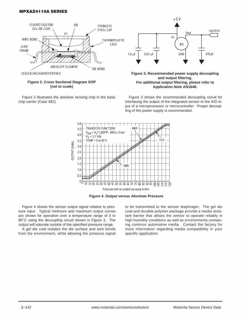
3–142 Motorola Sensor Device Datawww.motorola.com/semiconductors
WIRE BOND
STAINLESSSTEEL CAP
THERMOPLASTICCASE
DIE BONDSEALED VACUUM REFERENCE
DIE
P1
FLUORO SILICONEGEL DIE COAT
LEADFRAME
ABSOLUTE ELEMENT
Figure 2. Cross Sectional Diagram SOP(not to scale)
1.0 F
IPS
470 pF
OUTPUT
Vs
5 V
0.01 F GND
Vout
Figure 3. Recommended power supply decouplingand output filtering.
For additional output filtering, please refer toApplication Note AN1646.
Figure 2 illustrates the absolute sensing chip in the basicchip carrier (Case 482).
Figure 3 shows the recommended decoupling circuit forinterfacing the output of the integrated sensor to the A/D in-put of a microprocessor or microcontroller. Proper decoup-ling of the power supply is recommended.
OU
TPU
T (V
olts
)
5.0
4.5
4.0
3.5
3.0
Pressure (ref: to sealed vacuum) in kPa
TYP
MAX
MIN
5 10 15 20 25 30 35 40 45 50 55 60 65 70 75 80 85 90 95 100
105
2.5
2.0
1.5
1.0
0.5
0
110
Figure 4. Output versus Absolute Pressure
TRANSFER FUNCTION:Vout = Vs* (.009*P–.095) ± ErrorVS = 5.1 VdcTEMP = 0 to 85°C
115
120
Figure 4 shows the sensor output signal relative to pres-sure input. Typical minimum and maximum output curvesare shown for operation over a temperature range of 0 to85°C using the decoupling circuit shown in Figure 3. Theoutput will saturate outside of the specified pressure range.
A gel die coat isolates the die surface and wire bondsfrom the environment, while allowing the pressure signal
to be transmitted to the sensor diaphragm. The gel diecoat and durable polymer package provide a media resis-tant barrier that allows the sensor to operate reliably inhigh humidity conditions as well as environments contain-ing common automotive media. Contact the factory formore information regarding media compatibility in yourspecific application.
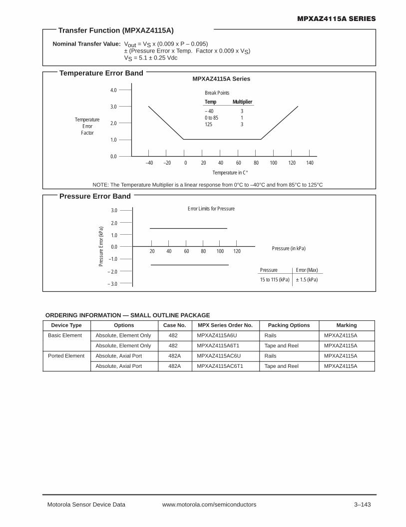
3–143Motorola Sensor Device Data www.motorola.com/semiconductors
Transfer Function (MPXAZ4115A)
Nominal Transfer Value: Vout = VS x (0.009 x P – 0.095)± (Pressure Error x Temp. Factor x 0.009 x VS)VS = 5.1 ± 0.25 Vdc
Temperature Error BandMPXAZ4115A Series
Break Points
Temp Multiplier
– 40 30 to 85 1125 3
Temperature in C°
4.0
3.0
2.0
0.0
1.0
–40 –20 0 20 40 60 14012010080
TemperatureError
Factor
NOTE: The Temperature Multiplier is a linear response from 0°C to –40°C and from 85°C to 125°C
Pressure Error Band
Error Limits for Pressure3.0
2.0
1.0
–1.0
– 2.0
– 3.0
0.020 Pressure (in kPa)
Pres
sure
Erro
r (kP
a)
Pressure Error (Max)
15 to 115 (kPa) ± 1.5 (kPa)
40 60 80 100 120
ORDERING INFORMATION — SMALL OUTLINE PACKAGE
Device Type Options Case No. MPX Series Order No. Packing Options Marking
Basic Element Absolute, Element Only 482 MPXAZ4115A6U Rails MPXAZ4115A
Absolute, Element Only 482 MPXAZ4115A6T1 Tape and Reel MPXAZ4115A
Ported Element Absolute, Axial Port 482A MPXAZ4115AC6U Rails MPXAZ4115A
Absolute, Axial Port 482A MPXAZ4115AC6T1 Tape and Reel MPXAZ4115A

3–144 Motorola Sensor Device Datawww.motorola.com/semiconductors
INFORMATION FOR USING THE SMALL OUTLINE PACKAGE (CASE 482)
MINIMUM RECOMMENDED FOOTPRINT FOR SURFACE MOUNTED APPLICATIONS
Surface mount board layout is a critical portion of the totaldesign. The footprint for the surface mount packages mustbe the correct size to ensure proper solder connection inter-face between the board and the package. With the correct
fottprint, the packages will self–align when subjected to asolder reflow process. It is always recommended to designboards with a solder mask layer to avoid bridging and short-ing between solder pads.
0.66016.76
0.060 TYP 8X1.52
0.100 TYP 8X2.54
0.100 TYP 8X2.54
0.3007.62
Figure 5. SOP Footprint (Case 482)
inchmm SCALE 2:1

3–145Motorola Sensor Device Data www.motorola.com/semiconductors
$$% % "#%&# &#' %#% ! #$$&# $!#!# $&# $!&% #$$&# " ! %! "#%&# !" $% #%
Motorola’s MPXAZ6115A series sensor integrates on–chip, bipolar op amp circuitryand thin film resistor networks to provide a high output signal and temperaturecompensation. The small form factor and high reliability of on–chip integration make theMotorola pressure sensor a logical and economical choice for the system designer.
The MPXAZ6115A series piezoresistive transducer is a state–of–the–art, monolithic,signal conditioned, silicon pressure sensor. This sensor combines advancedmicromachining techniques, thin film metallization, and bipolar semiconductor processingto provide an accurate, high level analog output signal that is proportional to appliedpressure.
Figure 1 shows a block diagram of the internal circuitry integrated on a pressuresensor chip.
Features
• Resistant to High Humidity and Common Automotive Media
• Improved Accuracy at High Temperature
• 1.5% Maximum Error over 0° to 85°C• Ideally suited for Microprocessor or Microcontroller–Based Systems
• Temperature Compensated from –40° to +125°C• Durable Thermoplastic (PPS) Surface Mount Package
Application Examples
• Aviation Altimeters
• Industrial Controls
• Engine Control/Manifold Absolute Pressure (MAP)
• Weather Station and Weather Reporting Devices
Figure 1. Fully Integrated Pressure SensorSchematic
VS
SENSINGELEMENT
Vout
GND
THIN FILMTEMPERATURECOMPENSATION
ANDGAIN STAGE #1
GAIN STAGE #2AND
GROUNDREFERENCE
SHIFT CIRCUITRY
PINS 1, 5, 6, 7 AND 8 ARE NO CONNECTS
SEMICONDUCTOR TECHNICAL DATA
5
6
7
8
N/C
VSGnd
Vout
N/C
N/C
N/C
INTEGRATEDPRESSURE SENSOR
15 to 115 kPa (2.2 to 16.7 psi)0.2 to 4.8 Volts Output
PIN NUMBER
NOTE: Pins 1, 5, 6, 7, and 8 are internaldevice connections. Do not connect toexternal circuitry or ground. Pin 1 isdenoted by the notch in the lead.
1
2
3
MPXAZ6115A6UCASE 482
MPXAZ6115AC6UCASE 482A
4 N/C
SMALL OUTLINE PACKAGE
REV 0

3–146 Motorola Sensor Device Datawww.motorola.com/semiconductors
MAXIMUM RATINGS(1)
Parametrics Symbol Value Units
Maximum Pressure (P1 P2) Pmax 400 kPa
Storage Temperature Tstg –40° to +125° °C
Operating Temperature TA –40° to +125° °C
Output Source Current @ Full Scale Output(2) Io+ 0.5 mAdc
Output Sink Current @ Minimum Pressure Offset(2) Io– –0.5 mAdc
NOTES:1. Exposure beyond the specified limits may cause permanent damage or degradation to the device.2. Maximum Output Current is controlled by effective impedance from Vout to Gnd or Vout to VS in the application circuit.
OPERATING CHARACTERISTICS (VS = 5.0 Vdc, TA = 25°C unless otherwise noted, P1 P2.)
Characteristic Symbol Min Typ Max Unit
Pressure Range POP 15 — 115 kPa
Supply Voltage(1) VS 4.75 5.0 5.25 Vdc
Supply Current Io — 6.0 10 mAdc
Minimum Pressure Offset(2) (0 to 85°C)@ VS = 5.0 Volts
Voff 0.133 0.200 0.268 Vdc
Full Scale Output(3) (0 to 85°C)@ VS = 5.0 Volts
VFSO 4.633 4.700 4.768 Vdc
Full Scale Span(4) (0 to 85°C)@ VS = 5.0 Volts
VFSS 4.433 4.500 4.568 Vdc
Accuracy(5) (0 to 85°C) — — — ±1.5 %VFSS
Sensitivity V/P — 45.9 — mV/kPa
Response Time(6) tR — 1.0 — ms
Warm–Up Time(7) — — 20 — ms
Offset Stability(8) — — ±0.25 — %VFSS
NOTES:1. Device is ratiometric within this specified excitation range.2. Offset (Voff) is defined as the output voltage at the minimum rated pressure.3. Full Scale Output (VFSO) is defined as the output voltage at the maximum or full rated pressure.4. Full Scale Span (VFSS) is defined as the algebraic difference between the output voltage at full rated pressure and the output voltage at the
minimum rated pressure.5. Accuracy is the deviation in actual output from nominal output over the entire pressure range and temperature range as a percent of span
at 25°C due to all sources of error including the following:• Linearity: Output deviation from a straight line relationship with pressure over the specified pressure range.• Temperature Hysteresis: Output deviation at any temperature within the operating temperature range, after the temperature is
cycled to and from the minimum or maximum operating temperature points, with zero differentialpressure applied.
• Pressure Hysteresis: Output deviation at any pressure within the specified range, when this pressure is cycled to and from minimum or maximum rated pressure at 25°C.
• TcSpan: Output deviation over the temperature range of 0° to 85°C, relative to 25°C.• TcOffset: Output deviation with minimum pressure applied, over the temperature range of 0° to 85°C, relative
to 25°C.6. Response Time is defined as the time for the incremental change in the output to go from 10% to 90% of its final value when subjected to
a specified step change in pressure.7. Warm–up Time is defined as the time required for the product to meet the specified output voltage after the pressure has been stabilized.8. Offset Stability is the product’s output deviation when subjected to 1000 cycles of Pulsed Pressure, Temperature Cycling with Bias Test.

3–147Motorola Sensor Device Data www.motorola.com/semiconductors
Figure 2. Cross Sectional Diagram SOP(Not to Scale)
Figure 3. Typical Application Circuit(Output Source Current Operation)
WIRE BOND
STAINLESSSTEEL CAP
THERMOPLASTICCASE
DIE BONDSEALED VACUUM REFERENCE
DIE
P1
FLUORO SILICONEGEL DIE COAT
LEADFRAME
ABSOLUTE ELEMENT VS Pin 2
5.0 V
GND Pin 3
Vout Pin 4
MPXAZ6115A
to ADC100 nF
51 K47 pF
Figure 2 illustrates the absolute sensing chip in the basicSmall Outline chip carrier (Case 482).
Figure 3 shows a typical application circuit (output sourcecurrent operation).
OU
TPU
T (V
olts
)
5.0
4.5
4.0
3.5
3.0
Pressure (ref: to sealed vacuum) in kPa
TYP
MAX
MIN
5 10 15 20 25 30 35 40 45 50 55 60 65 70 75 80 85 90 95 100
105
2.5
2.0
1.5
1.0
0.5
0
110
Figure 4. Output versus Absolute Pressure
TRANSFER FUNCTION:Vout = Vs* (.009*P–.095) ± ErrorVS = 5.0 VdcTEMP = 0 to 85°C
115
120
Figure 4 shows the sensor output signal relative to pres-sure input. Typical minimum and maximum output curvesare shown for operation over 0 to 85°C temperature range.The output will saturate outside of the rated pressure range.
A gel die coat isolates the die surface and wire bondsfrom the environment, while allowing the pressure signalto be transmitted to the sensor diaphragm. The gel die
coat and durable polymer package provide a media resis-tant barrier that allows the sensor to operate reliably inhigh humidity conditions as well as environments contain-ing common automotive media. Contact the factory formore information regarding media compatibility in yourspecific application.
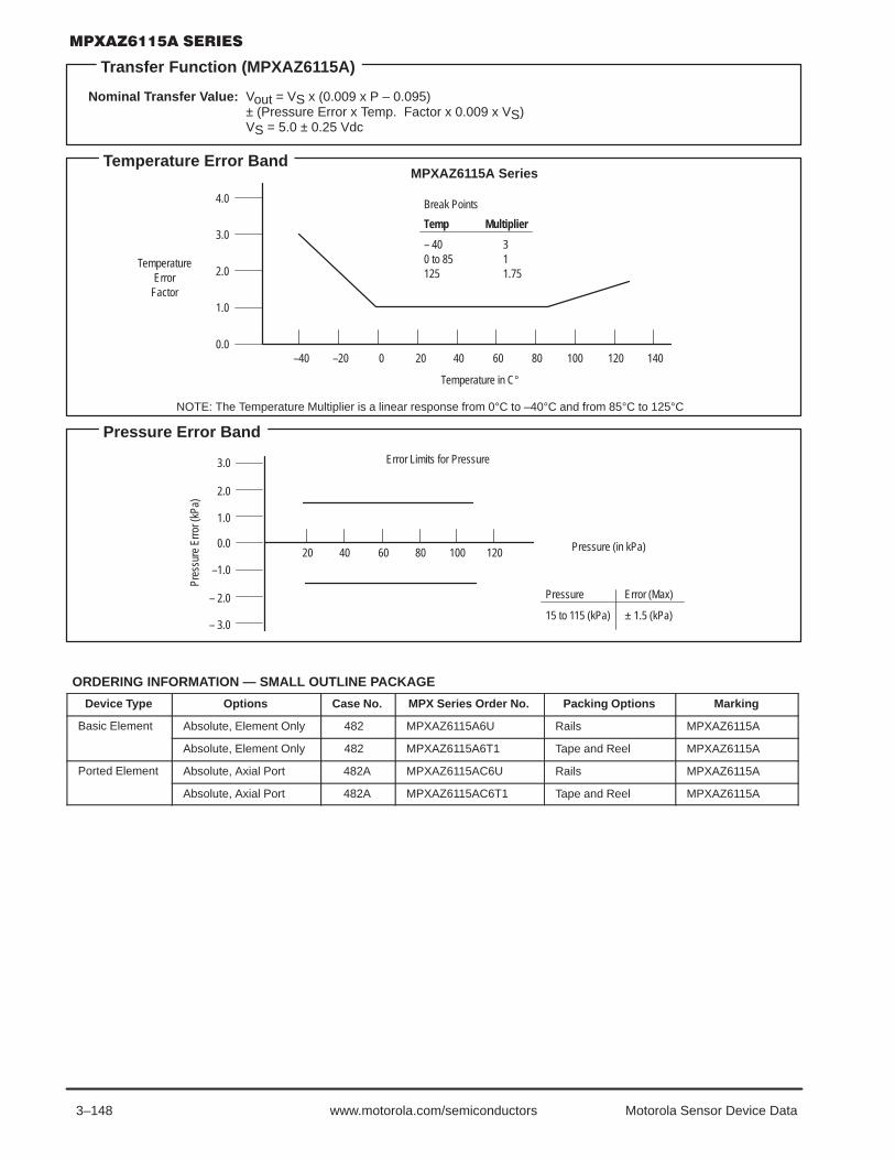
3–148 Motorola Sensor Device Datawww.motorola.com/semiconductors
Transfer Function (MPXAZ6115A)
Nominal Transfer Value: Vout = VS x (0.009 x P – 0.095)± (Pressure Error x Temp. Factor x 0.009 x VS)VS = 5.0 ± 0.25 Vdc
Temperature Error BandMPXAZ6115A Series
Break Points
Temp Multiplier
– 40 30 to 85 1125 1.75
Temperature in C°
4.0
3.0
2.0
0.0
1.0
–40 –20 0 20 40 60 14012010080
TemperatureError
Factor
NOTE: The Temperature Multiplier is a linear response from 0°C to –40°C and from 85°C to 125°C
Pressure Error Band
Error Limits for Pressure3.0
2.0
1.0
–1.0
– 2.0
– 3.0
0.020 Pressure (in kPa)
Pres
sure
Erro
r (kP
a)
Pressure Error (Max)
15 to 115 (kPa) ± 1.5 (kPa)
40 60 80 100 120
ORDERING INFORMATION — SMALL OUTLINE PACKAGE
Device Type Options Case No. MPX Series Order No. Packing Options Marking
Basic Element Absolute, Element Only 482 MPXAZ6115A6U Rails MPXAZ6115A
Absolute, Element Only 482 MPXAZ6115A6T1 Tape and Reel MPXAZ6115A
Ported Element Absolute, Axial Port 482A MPXAZ6115AC6U Rails MPXAZ6115A
Absolute, Axial Port 482A MPXAZ6115AC6T1 Tape and Reel MPXAZ6115A

3–149Motorola Sensor Device Data www.motorola.com/semiconductors
SURFACE MOUNTING INFORMATION
MINIMUM RECOMMENDED FOOTPRINT FOR SMALL OUTLINE PACKAGE
Surface mount board layout is a critical portion of the totaldesign. The footprint for the semiconductor package mustbe the correct size to ensure proper solder connection inter-face between the board and the package. With the correctpad geometry, the packages will self–align when subjected to
a solder reflow process. It is always recommended to fabri-cate boards with a solder mask layer to avoid bridging and/orshorting between solder pads, especially on tight tolerancesand/or tight layouts.
0.66016.76
0.060 TYP 8X1.52
0.100 TYP 8X2.54
0.100 TYP2.54
0.3007.62
Figure 5. SOP Footprint (Case 482 and 482A)
inchmm

3–150 Motorola Sensor Device Datawww.motorola.com/semiconductors
! " !
Motorola has developed a low cost, high volume, miniature pressure sensor packagewhich is ideal as a sub–module component or a disposable unit. The unique concept ofthe Chip Pak allows great flexibility in system design while allowing an economic solutionfor the designer. This new chip carrier package uses Motorola’s unique sensor die with itspiezoresistive technology, along with the added feature of on–chip, thin–film temperaturecompensation and calibration.
NOTE: Motorola is also offering the Chip Pak package in application–specificconfigurations, which will have an “SPX” prefix, followed by a four–digit number, uniqueto the specific customer.
Features:
• Low Cost
• Integrated Temperature Compensation and Calibration
• Ratiometric to Supply Voltage
• Polysulfone Case Material (Medical, Class V Approved)
• Provided in Easy–to–Use Tape and Reel
Application Examples
• Respiratory Diagnostics
• Air Movement Control
• Controllers
• Pressure Switching
NOTE: The die and wire bonds are exposed on the front side of the Chip Pak(pressure is applied to the backside of the device). Front side die and wire protectionmust be provided in the customer’s housing. Use caution when handling the devicesduring all processes.
Motorola’s MPXC2011DT1/MPXC2012DT1 PressureSensor has been designed for medical usage by combiningthe performance of Motorola’s shear stress pressure sensordesign and the use of biomedically approved materials.Materials with a proven history in medical situations havebeen chosen to provide a sensor that can be used withconfidence in applications, such as invasive blood pressuremonitoring. It can be sterilized using ethylene oxide. Theportions of the pressure sensor that are required to bebiomedically approved are the rigid housing and the gelcoating.
The rigid housing is molded from a white, medical gradepolysulfone that has passed extensive biological testingincluding: tissue culture test, rabbit implant, hemolysis,intracutaneous test in rabbits, and system toxicity, USP.
The MPXC2011DT1 contains a silicone dielectric gelwhich covers the silicon piezoresistive sensing element. Thegel is a nontoxic, nonallergenic elastomer system whichmeets all USP XX Biological Testing Class V requirements.The properties of the gel allow it to transmit pressure uni-formly to the diaphragm surface, while isolating the internalelectrical connections from the corrosive effects of fluids,such as saline solution. The gel provides electrical isolationsufficient to withstand defibrillation testing, as specified in theproposed Association for the Advancement of MedicalInstrumentation (AAMI) Standard for blood pressure trans-ducers. A biomedically approved opaque filler in the gel pre-vents bright operating room lights from affecting theperformance of the sensor.
The MPXC2012DT1 is a no–gel option.
Preferred devices are Motorola recommended choices for future use and best overall value.
SEMICONDUCTOR TECHNICAL DATA
PRESSURE SENSORS0 to 75 mmHg (0 to 10 kPa)
PIN NUMBER
MPXC2011DT1/MPXC2012DT1CASE 423A
1
2
Gnd
S+
3
4
VS
S–
CHIP PAK PACKAGE
Motorola Preferred Device
REV 2

3–151Motorola Sensor Device Data www.motorola.com/semiconductors
MAXIMUM RATINGS(NOTE)
Rating Symbol Value Unit
Maximum Pressure (Backside) Pmax 75 kPa
Storage Temperature Tstg –25 to +85 °C
Operating Temperature TA +15 to +40 °C
NOTE: Exposure beyond the specified limits may cause permanent damage or degradation to the device.
OPERATING CHARACTERISTICS (VS = 10 Vdc, TA = 25°C unless otherwise noted, P1 > P2)
Characteristic Symbol Min Typ Max Unit
Pressure Range(1) POP 0 — 10 kPa
Supply Voltage(2) VS — 3 10 Vdc
Supply Current Io — 6.0 — mAdc
Full Scale Span(3) VFSS 24 25 26 mV
Offset(4) Voff –1.0 — 1.0 mV
Sensitivity ∆V/∆P — 2.5 — mV/kPa
Linearity(5) — –1.0 — 1.0 %VFSS
Pressure Hysteresis(5) (0 to 10 kPa) — — ±0.1 — %VFSS
Temperature Hysteresis(5) (+15°C to +40°C) — — ±0.1 — %VFSS
Temperature Effect on Full Scale Span(5) TCVFSS –1.0 — 1.0 %VFSS
Temperature Effect on Offset(5) TCVoff –1.0 — 1.0 mV
Input Impedance Zin 1300 — 2550 Ω
Output Impedance Zout 1400 — 3000 Ω
Response Time(6) (10% to 90%) tR — 1.0 — ms
Warm–Up — — 20 — ms
Offset Stability(7) — — ±0.5 — %VFSS
NOTES:1. 1.0 kPa (kiloPascal) equals 0.145 psi.2. Device is ratiometric within this specified excitation range. Operating the device above the specified excitation range may induce additional
error due to device self–heating.3. Full Scale Span (VFSS) is defined as the algebraic difference between the output voltage at full rated pressure and the output voltage at the
minimum rated pressure.4. Offset (Voff) is defined as the output voltage at the minimum rated pressure.5. Accuracy (error budget) consists of the following:
• Linearity: Output deviation from a straight line relationship with pressure, using end point method, over the specified pressure range.
• Temperature Hysteresis: Output deviation at any temperature within the operating temperature range, after the temperature is cycled to and from the minimum or maximum operating temperature points, with zero differential pressure applied.
• Pressure Hysteresis: Output deviation at any pressure within the specified range, when this pressure is cycled to and from the minimum or maximum rated pressure, at 25°C.
• TcSpan: Output deviation at full rated pressure over the temperature range of 0 to 85°C, relative to 25°C.• TcOffset: Output deviation with minimum rated pressure applied, over the temperature range of 0 to 85°C, relative
to 25°C.6. Response Time is defined as the time for the incremental change in the output to go from 10% to 90% of its final value when subjected to
a specified step change in pressure.7. Offset stability is the product’s output deviation when subjected to 1000 hours of Pulsed Pressure, Temperature Cycling with Bias Test.

3–152 Motorola Sensor Device Datawww.motorola.com/semiconductors
ORDERING INFORMATION
The MPXC2011DT1/MPXC2012DT1 silicon pressure sensors are available in tape and reel.
Device Type/Order No. Case No. Device Description Marking
MPXC2011DT1 423A Chip Pak, 1/3 Gel Date Code, Lot ID
MPXC2012DT1 423A Chip Pak, No Gel Date Code, Lot ID
Packaging Information Reel Size Tape Width Quantity
Tape and Reel 330 mm 24 mm 1000 pc/reel
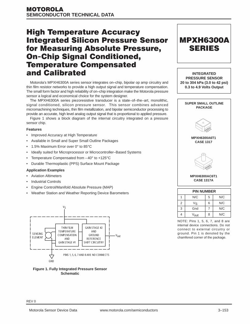
3–153Motorola Sensor Device Data www.motorola.com/semiconductors
!"$%" %"&$"$ "##%" # " " #%" # %$ "##%"! $ !"$%" !#$ "$
Motorola’s MPXH6300A series sensor integrates on–chip, bipolar op amp circuitry andthin film resistor networks to provide a high output signal and temperature compensation.The small form factor and high reliability of on–chip integration make the Motorola pressuresensor a logical and economical choice for the system designer.
The MPXH6300A series piezoresistive transducer is a state–of–the–art, monolithic,signal conditioned, silicon pressure sensor. This sensor combines advancedmicromachining techniques, thin film metallization, and bipolar semiconductor processing toprovide an accurate, high level analog output signal that is proportional to applied pressure.
Figure 1 shows a block diagram of the internal circuitry integrated on a pressuresensor chip.
Features
• Improved Accuracy at High Temperature
• Available in Small and Super Small Outline Packages
• 1.5% Maximum Error over 0° to 85°C• Ideally suited for Microprocessor or Microcontroller–Based Systems
• Temperature Compensated from –40° to +125°C• Durable Thermoplastic (PPS) Surface Mount Package
Application Examples
• Aviation Altimeters
• Industrial Controls
• Engine Control/Manifold Absolute Pressure (MAP)
• Weather Station and Weather Reporting Device Barometers
Figure 1. Fully Integrated Pressure SensorSchematic
VS
SENSINGELEMENT
Vout
GND
THIN FILMTEMPERATURECOMPENSATION
ANDGAIN STAGE #1
GAIN STAGE #2AND
GROUNDREFERENCE
SHIFT CIRCUITRY
PINS 1, 5, 6, 7 AND 8 ARE NO CONNECTS
SEMICONDUCTOR TECHNICAL DATA
INTEGRATEDPRESSURE SENSOR
20 to 304 kPa (3.0 to 42 psi)0.3 to 4.9 Volts Output
PIN NUMBER
NOTE: Pins 1, 5, 6, 7, and 8 areinternal device connections. Do notconnect to external circuitry orground. Pin 1 is denoted by thechamfered corner of the package.
1
2
3
N/C
VSGnd
5
6
7
N/C
N/C
N/C
MPXH6300A6T1CASE 1317
MPXH6300AC6T1CASE 1317A
4 Vout 8 N/C
SUPER SMALL OUTLINEPACKAGE
REV 0
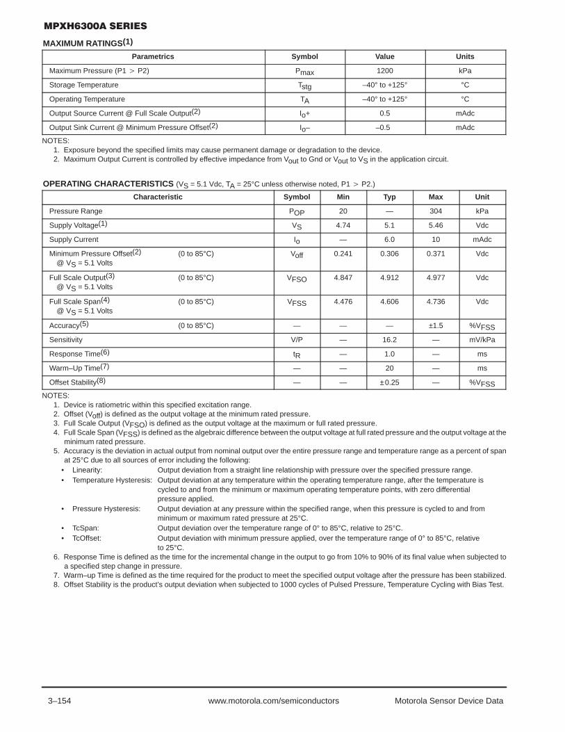
3–154 Motorola Sensor Device Datawww.motorola.com/semiconductors
MAXIMUM RATINGS(1)
Parametrics Symbol Value Units
Maximum Pressure (P1 P2) Pmax 1200 kPa
Storage Temperature Tstg –40° to +125° °C
Operating Temperature TA –40° to +125° °C
Output Source Current @ Full Scale Output(2) Io+ 0.5 mAdc
Output Sink Current @ Minimum Pressure Offset(2) Io– –0.5 mAdc
NOTES:1. Exposure beyond the specified limits may cause permanent damage or degradation to the device.2. Maximum Output Current is controlled by effective impedance from Vout to Gnd or Vout to VS in the application circuit.
OPERATING CHARACTERISTICS (VS = 5.1 Vdc, TA = 25°C unless otherwise noted, P1 P2.)
Characteristic Symbol Min Typ Max Unit
Pressure Range POP 20 — 304 kPa
Supply Voltage(1) VS 4.74 5.1 5.46 Vdc
Supply Current Io — 6.0 10 mAdc
Minimum Pressure Offset(2) (0 to 85°C)@ VS = 5.1 Volts
Voff 0.241 0.306 0.371 Vdc
Full Scale Output(3) (0 to 85°C)@ VS = 5.1 Volts
VFSO 4.847 4.912 4.977 Vdc
Full Scale Span(4) (0 to 85°C)@ VS = 5.1 Volts
VFSS 4.476 4.606 4.736 Vdc
Accuracy(5) (0 to 85°C) — — — ±1.5 %VFSS
Sensitivity V/P — 16.2 — mV/kPa
Response Time(6) tR — 1.0 — ms
Warm–Up Time(7) — — 20 — ms
Offset Stability(8) — — ±0.25 — %VFSS
NOTES:1. Device is ratiometric within this specified excitation range.2. Offset (Voff) is defined as the output voltage at the minimum rated pressure.3. Full Scale Output (VFSO) is defined as the output voltage at the maximum or full rated pressure.4. Full Scale Span (VFSS) is defined as the algebraic difference between the output voltage at full rated pressure and the output voltage at the
minimum rated pressure.5. Accuracy is the deviation in actual output from nominal output over the entire pressure range and temperature range as a percent of span
at 25°C due to all sources of error including the following:• Linearity: Output deviation from a straight line relationship with pressure over the specified pressure range.• Temperature Hysteresis: Output deviation at any temperature within the operating temperature range, after the temperature is
cycled to and from the minimum or maximum operating temperature points, with zero differentialpressure applied.
• Pressure Hysteresis: Output deviation at any pressure within the specified range, when this pressure is cycled to and from minimum or maximum rated pressure at 25°C.
• TcSpan: Output deviation over the temperature range of 0° to 85°C, relative to 25°C.• TcOffset: Output deviation with minimum pressure applied, over the temperature range of 0° to 85°C, relative
to 25°C.6. Response Time is defined as the time for the incremental change in the output to go from 10% to 90% of its final value when subjected to
a specified step change in pressure.7. Warm–up Time is defined as the time required for the product to meet the specified output voltage after the pressure has been stabilized.8. Offset Stability is the product’s output deviation when subjected to 1000 cycles of Pulsed Pressure, Temperature Cycling with Bias Test.

3–155Motorola Sensor Device Data www.motorola.com/semiconductors
Figure 2. Cross Sectional Diagram SSOP(not to scale)
Figure 3. Typical Application Circuit(Output Source Current Operation)
WIRE BOND
STAINLESSSTEEL CAP
THERMOPLASTICCASE
DIE BONDSEALED VACUUM REFERENCE
DIE
P1
FLUORO SILICONEGEL DIE COAT
LEADFRAME
ABSOLUTE ELEMENT
VS Pin 2
5.1 V
GND Pin 3
Vout Pin 4 to ADC100 nF
51 K47 pF
MPXH6300A
Figure 2 illustrates the absolute sensing chip in the basicSuper Small Outline chip carrier (Case 1317).
Figure 3 shows a typical application circuit (output sourcecurrent operation).
OU
TPU
T (V
olts
)
5.0
4.5
4.0
3.5
3.0
Pressure (ref: to sealed vacuum) in kPa
TYP
MAX
MIN
20 35 50 65 80 95 110
125
140
155
170
185
200
215
230
245
260
275
2.5
2.0
1.5
1.0
0.5
0
290
Figure 4. Output versus Absolute Pressure
TRANSFER FUNCTION:Vout = Vs* (.00318*P–.00353) ± ErrorVS = 5.1 VdcTEMP = 0 to 85°C
305
Figure 4 shows the sensor output signal relative to pres-sure input. Typical minimum and maximum output curvesare shown for operation over 0 to 85°C temperature range.The output will saturate outside of the rated pressure range.
A fluorosilicone gel isolates the die surface and wirebonds from the environment, while allowing the pressuresignal to be transmitted to the silicon diaphragm. The
MPXH6300A series pressure sensor operating characteris-tics, internal reliability and qualification tests are based onuse of dry air as the pressure media. Media other than dryair may have adverse effects on sensor performance andlong–term reliability. Contact the factory for information re-garding media compatibility in your application.

3–156 Motorola Sensor Device Datawww.motorola.com/semiconductors
Transfer Function (MPXH6300A)
Nominal Transfer Value: Vout = VS x (0.00318 x P – 0.00353)± (Pressure Error x Temp. Factor x 0.00318 x VS)VS = 5.1 ± 0.36 Vdc
Temperature Error BandMPXH6300A Series
Break Points
Temp Multiplier
– 40 30 to 85 1125 3
Temperature in C°
4.0
3.0
2.0
0.0
1.0
–40 –20 0 20 40 60 14012010080
TemperatureError
Factor
NOTE: The Temperature Multiplier is a linear response from 0°C to –40°C and from 85°C to 125°C
Pressure Error Band
Error Limits for Pressure
3.0
2.0
1.0
–1.0
– 2.0
–4.0
0.020 Pressure (in kPa)
Pres
sure
Erro
r (kP
a)
Pressure Error (Max)
20 to 304 (kPa) ± 4.0 (kPa)
60 100
4.0
– 3.0
140 180 220 260 300
ORDERING INFORMATION — SUPER SMALL OUTLINE PACKAGE
Device Type Options Case No. MPX Series Order No. Packing Options Marking
Basic Element Absolute, Element Only 1317 MPXH6300A6U Rails MPXH6300A
Absolute, Element Only 1317 MPXH6300A6T1 Tape and Reel MPXH6300A
Ported Element Absolute, Axial Port 1317A MPXH6300AC6U Rails MPXH6300A
Absolute, Axial Port 1317A MPXH6300AC6T1 Tape and Reel MPXH6300A

3–157Motorola Sensor Device Data www.motorola.com/semiconductors
SURFACE MOUNTING INFORMATION
MINIMUM RECOMMENDED FOOTPRINT FOR SUPER SMALL OUTLINE PACKAGES
Surface mount board layout is a critical portion of the totaldesign. The footprint for the semiconductor package mustbe the correct size to ensure proper solder connection inter-face between the board and the package. With the correctpad geometry, the packages will self–align when subjected to
a solder reflow process. It is always recommended to fabri-cate boards with a solder mask layer to avoid bridging and/orshorting between solder pads, especially on tight tolerancesand/or tight layouts.
Figure 5. SSOP Footprint (Case 1317 and 1317A)
0.027 TYP 8X0.69
0.053 TYP 8X1.35
inchmm
0.3879.83
0.1503.81
0.0501.27TYP
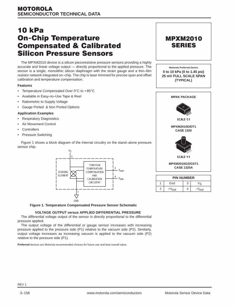
3–158 Motorola Sensor Device Datawww.motorola.com/semiconductors
"# !" " !!# ! !
The MPXM2010 device is a silicon piezoresistive pressure sensors providing a highlyaccurate and linear voltage output — directly proportional to the applied pressure. Thesensor is a single, monolithic silicon diaphragm with the strain gauge and a thin–filmresistor network integrated on–chip. The chip is laser trimmed for precise span and offsetcalibration and temperature compensation.
Features
• Temperature Compensated Over 0°C to +85°C• Available in Easy–to–Use Tape & Reel
• Ratiometric to Supply Voltage
• Gauge Ported & Non Ported Options
Application Examples
• Respiratory Diagnostics
• Air Movement Control
• Controllers
• Pressure Switching
Figure 1 shows a block diagram of the internal circuitry on the stand–alone pressuresensor chip.
Figure 1. Temperature Compensated Pressure Sensor Schematic
VS
3
SENSINGELEMENT
THIN FILMTEMPERATURECOMPENSATION
ANDCALIBRATION
CIRCUITRY
2
4
Vout+
Vout–
1
GND
VOLTAGE OUTPUT versus APPLIED DIFFERENTIAL PRESSUREThe differential voltage output of the sensor is directly proportional to the differential
pressure applied.The output voltage of the differential or gauge sensor increases with increasing
pressure applied to the pressure side (P1) relative to the vacuum side (P2). Similarly,output voltage increases as increasing vacuum is applied to the vacuum side (P2)relative to the pressure side (P1).
Preferred devices are Motorola recommended choices for future use and best overall value.
SEMICONDUCTOR TECHNICAL DATA
0 to 10 kPa (0 to 1.45 psi)25 mV FULL SCALE SPAN
(TYPICAL)
PIN NUMBER
1
2
Gnd
+Vout
3
4
VS
–Vout
Motorola Preferred Device
MPXM2010D/DT1CASE 1320
MPXM2010GS/GST1CASE 1320A
SCALE 1:1
SCALE 1:1
MPAK PACKAGE
REV 1
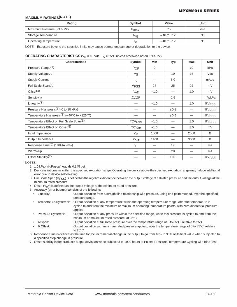
3–159Motorola Sensor Device Data www.motorola.com/semiconductors
MAXIMUM RATINGS(NOTE)
Rating Symbol Value Unit
Maximum Pressure (P1 > P2) Pmax 75 kPa
Storage Temperature Tstg –40 to +125 °C
Operating Temperature TA –40 to +125 °C
NOTE: Exposure beyond the specified limits may cause permanent damage or degradation to the device.
OPERATING CHARACTERISTICS (VS = 10 Vdc, TA = 25°C unless otherwise noted, P1 > P2)
Characteristic Symbol Min Typ Max Unit
Pressure Range(1) POP 0 — 10 kPa
Supply Voltage(2) VS — 10 16 Vdc
Supply Current Io — 6.0 — mAdc
Full Scale Span(3) VFSS 24 25 26 mV
Offset(4) Voff –1.0 — 1.0 mV
Sensitivity ∆V/∆P — 2.5 — mV/kPa
Linearity(5) — –1.0 — 1.0 %VFSS
Pressure Hysteresis(5) (0 to 10 kPa) — — ±0.1 — %VFSS
Temperature Hysteresis(5) (–40°C to +125°C) — — ±0.5 — %VFSS
Temperature Effect on Full Scale Span(5) TCVFSS –1.0 — 1.0 %VFSS
Temperature Effect on Offset(5) TCVoff –1.0 — 1.0 mV
Input Impedance Zin 1000 — 2550 Ω
Output Impedance Zout 1400 — 3000 Ω
Response Time(6) (10% to 90%) tR — 1.0 — ms
Warm–Up — — 20 — ms
Offset Stability(7) — — ±0.5 — %VFSS
NOTES:1. 1.0 kPa (kiloPascal) equals 0.145 psi.2. Device is ratiometric within this specified excitation range. Operating the device above the specified excitation range may induce additional
error due to device self–heating.3. Full Scale Span (VFSS) is defined as the algebraic difference between the output voltage at full rated pressure and the output voltage at the
minimum rated pressure.4. Offset (Voff) is defined as the output voltage at the minimum rated pressure.5. Accuracy (error budget) consists of the following:
• Linearity: Output deviation from a straight line relationship with pressure, using end point method, over the specified pressure range.
• Temperature Hysteresis: Output deviation at any temperature within the operating temperature range, after the temperature is cycled to and from the minimum or maximum operating temperature points, with zero differential pressure applied.
• Pressure Hysteresis: Output deviation at any pressure within the specified range, when this pressure is cycled to and from the minimum or maximum rated pressure, at 25°C.
• TcSpan: Output deviation at full rated pressure over the temperature range of 0 to 85°C, relative to 25°C.• TcOffset: Output deviation with minimum rated pressure applied, over the temperature range of 0 to 85°C, relative
to 25°C.6. Response Time is defined as the time for the incremental change in the output to go from 10% to 90% of its final value when subjected to
a specified step change in pressure.7. Offset stability is the product’s output deviation when subjected to 1000 hours of Pulsed Pressure, Temperature Cycling with Bias Test.

3–160 Motorola Sensor Device Datawww.motorola.com/semiconductors
LINEARITYLinearity refers to how well a transducer’s output follows
the equation: Vout = Voff + sensitivity x P over the operatingpressure range. There are two basic methods for calculatingnonlinearity: (1) end point straight line fit (see Figure 2) or (2)a least squares best line fit. While a least squares fit givesthe “best case” linearity error (lower numerical value), thecalculations required are burdensome.
Conversely, an end point fit will give the “worst case” error(often more desirable in error budget calculations) and the cal-culations are more straightforward for the user. Motorola’sspecified pressure sensor linearities are based on the endpoint straight line method measured at the midrange pressure.
Figure 2. Linearity Specification Comparison
LEASTSQUAREDEVIATION
REL
ATIV
E VO
LTAG
E O
UTP
UT
PRESSURE (% FULLSCALE)0 50 100
END POINTSTRAIGHT LINE FIT
EXAGGERATED PERFORMANCECURVE
LEAST SQUARES FIT
STRAIGHT LINEDEVIATION
OFFSET
ON–CHIP TEMPERATURE COMPENSATION and CALIBRATION
Figure 3 shows the minimum, maximum and typical outputcharacteristics of the MPXM2010 series at 25°C. The outputis directly proportional to the differential pressure and is es-sentially a straight line.
A silicone gel isolates the die surface and wire bonds fromthe environment, while allowing the pressure signal to betransmitted to the silicon diaphragm.
Figure 3. Output versus Pressure Differential
MIN
TYP
OFFSET(TYP)
30
20
15
10
5
OU
TPU
T (m
Vdc)
25
0
– 5kPaPSI
2.50.362
50.725
7.51.09
101.45
aMAX SPANRANGE(TYP)
VS = 10 VdcTA = 25°CP1 > P2
ORDERING INFORMATION
Device Type Options Case NoDevice Type Options Case No.
MPXM2010D Non–ported 1320
MPXM2010DT1 Non–ported, Tape and Reel 1320
MPXM2010GS Ported 1320A
MPXM2010GST1 Ported, Tape and Reel 1320A

3–161Motorola Sensor Device Data www.motorola.com/semiconductors
!#$! "# !# !""$! "!"
The MPXM2053 device is a silicon piezoresistive pressure sensor providing a highlyaccurate and linear voltage output — directly proportional to the applied pressure. Thesensor is a single, monolithic silicon diaphragm with the strain gauge and a thin–filmresistor network integrated on–chip. The chip is laser trimmed for precise span and offsetcalibration and temperature compensation.
Features
• Temperature Compensated Over 0°C to +85°C• Available in Easy–to–Use Tape & Reel
• Ratiometric to Supply Voltage
• Gauge Ported & Non Ported Options
Application Examples
• Pump/Motor Controllers
• Robotics
• Level Indicators
• Medical Diagnostics
• Pressure Switching
• Non–Invasive Blood Pressure Measurement
Figure 1 shows a block diagram of the internal circuitry on the stand–alone pressuresensor chip.
Figure 1. Temperature Compensated Pressure Sensor Schematic
VS
3
X–ducerSENSINGELEMENT
THIN FILMTEMPERATURECOMPENSATION
ANDCALIBRATION
CIRCUITRY
2
4
Vout+
Vout–
1
GND
VOLTAGE OUTPUT versus APPLIED DIFFERENTIAL PRESSUREThe differential voltage output of the sensor is directly proportional to the differential
pressure applied.The output voltage of the differential or gauge sensor increases with increasing
pressure applied to the pressure side (P1) relative to the vacuum side (P2). Similarly,output voltage increases as increasing vacuum is applied to the vacuum side (P2)relative to the pressure side (P1).
Preferred devices are Motorola recommended choices for future use and best overall value.
SEMICONDUCTOR TECHNICAL DATA
0 to 50 kPa (0 to 7.25 psi)40 mV FULL SCALE SPAN
(TYPICAL)
PIN NUMBER
1
2
Gnd
+Vout
3
4
VS
–Vout
Motorola Preferred Device
MPXM2053D/DT1CASE 1320
MPXM2053GS/GST1CASE 1320A
SCALE 1:1
SCALE 1:1
MPAK PACKAGE
REV 1

3–162 Motorola Sensor Device Datawww.motorola.com/semiconductors
MAXIMUM RATINGS(NOTE)
Rating Symbol Value Unit
Maximum Pressure (P1 > P2) Pmax 200 kPa
Storage Temperature Tstg –40 to +125 °C
Operating Temperature TA –40 to +125 °C
NOTE: Exposure beyond the specified limits may cause permanent damage or degradation to the device.
OPERATING CHARACTERISTICS (VS = 10 Vdc, TA = 25°C unless otherwise noted, P1 > P2)
Characteristic Symbol Min Typ Max Unit
Pressure Range(1) POP 0 — 50 kPa
Supply Voltage(2) VS — 10 16 Vdc
Supply Current Io — 6.0 — mAdc
Full Scale Span(3) VFSS 38.5 40 41.5 mV
Offset(4) Voff –1.0 — 1.0 mV
Sensitivity ∆V/∆P — 0.8 — mV/kPa
Linearity(5) — –0.6 — 0.4 %VFSS
Pressure Hysteresis(5) (0 to 50 kPa) — — ±0.1 — %VFSS
Temperature Hysteresis(5) (–40°C to +125°C) — — ±0.5 — %VFSS
Temperature Effect on Full Scale Span(5) TCVFSS –2.0 — 2.0 %VFSS
Temperature Effect on Offset(5) TCVoff –1.0 — 1.0 mV
Input Impedance Zin 1000 — 2500 Ω
Output Impedance Zout 1400 — 3000 Ω
Response Time(6) (10% to 90%) tR — 1.0 — ms
Warm–Up — — 20 — ms
Offset Stability(7) — — ±0.5 — %VFSS
NOTES:1. 1.0 kPa (kiloPascal) equals 0.145 psi.2. Device is ratiometric within this specified excitation range. Operating the device above the specified excitation range may induce additional
error due to device self–heating.3. Full Scale Span (VFSS) is defined as the algebraic difference between the output voltage at full rated pressure and the output voltage at the
minimum rated pressure.4. Offset (Voff) is defined as the output voltage at the minimum rated pressure.5. Accuracy (error budget) consists of the following:
• Linearity: Output deviation from a straight line relationship with pressure, using end point method, over the specified pressure range.
• Temperature Hysteresis: Output deviation at any temperature within the operating temperature range, after the temperature is cycled to and from the minimum or maximum operating temperature points, with zero differential pressure applied.
• Pressure Hysteresis: Output deviation at any pressure within the specified range, when this pressure is cycled to and from the minimum or maximum rated pressure, at 25°C.
• TcSpan: Output deviation at full rated pressure over the temperature range of 0 to 85°C, relative to 25°C.• TcOffset: Output deviation with minimum rated pressure applied, over the temperature range of 0 to 85°C, relative
to 25°C.6. Response Time is defined as the time for the incremental change in the output to go from 10% to 90% of its final value when subjected to
a specified step change in pressure.7. Offset stability is the product’s output deviation when subjected to 1000 hours of Pulsed Pressure, Temperature Cycling with Bias Test.

3–163Motorola Sensor Device Data www.motorola.com/semiconductors
LINEARITYLinearity refers to how well a transducer’s output follows
the equation: Vout = Voff + sensitivity x P over the operatingpressure range. There are two basic methods for calculatingnonlinearity: (1) end point straight line fit (see Figure 2) or (2)a least squares best line fit. While a least squares fit givesthe “best case” linearity error (lower numerical value), thecalculations required are burdensome.
Conversely, an end point fit will give the “worst case” error(often more desirable in error budget calculations) and the cal-culations are more straightforward for the user. Motorola’sspecified pressure sensor linearities are based on the endpoint straight line method measured at the midrange pressure.
Figure 2. Linearity Specification Comparison
LEASTSQUAREDEVIATION
REL
ATIV
E VO
LTAG
E O
UTP
UT
PRESSURE (% FULLSCALE)0 50 100
END POINTSTRAIGHT LINE FIT
EXAGGERATED PERFORMANCECURVE
LEAST SQUARES FIT
STRAIGHT LINEDEVIATION
OFFSET
ON–CHIP TEMPERATURE COMPENSATION and CALIBRATION
Figure 3 shows the minimum, maximum and typical outputcharacteristics of the MPXM2053 series at 25°C. The outputis directly proportional to the differential pressure and is es-sentially a straight line.
A silicone gel isolates the die surface and wire bonds fromthe environment, while allowing the pressure signal to betransmitted to the silicon diaphragm.
Figure 3. Output versus Pressure Differential
OU
TPU
T (m
Vdc)
kPaPSI
40
35
30
25
15
10
5
0– 5
0 12.51.8
253.6
37.55.4
507.25
SPANRANGE(TYP)
OFFSET(TYP)
20MAX
TYP
MIN
VS = 10 VdcTA = 25°CP1 > P2
ORDERING INFORMATION
Device Type Options Case NoDevice Type Options Case No.
MPXM2053D Non–ported 1320
MPXM2053DT1 Non–ported, Tape and Reel 1320
MPXM2053GS Ported 1320A
MPXM2053GST1 Ported, Tape and Reel 1320A

3–164 Motorola Sensor Device Datawww.motorola.com/semiconductors
"# !" " !!# ! !
The MPXM2102 device is a silicon piezoresistive pressure sensors providing a highlyaccurate and linear voltage output — directly proportional to the applied pressure. Thesensor is a single, monolithic silicon diaphragm with the strain gauge and a thin–filmresistor network integrated on–chip. The chip is laser trimmed for precise span and offsetcalibration and temperature compensation.
Features
• Temperature Compensated Over 0°C to +85°C• Available in Easy-to-Use Tape & Reel
• Ratiometric to Supply Voltage
• Gauge Ported & Non Ported Options
Application Examples• Pump/Motor Controllers• Robotics• Level Indicators• Medical Diagnostics• Pressure Switching• Barometers• Altimeters
Figure 1 shows a block diagram of the internal circuitry on the stand–alone pressuresensor chip.
Figure 1. Temperature Compensated Pressure Sensor Schematic
VS
3
X–ducerSENSINGELEMENT
THIN FILMTEMPERATURECOMPENSATION
ANDCALIBRATION
CIRCUITRY
2
4
Vout+
Vout–
1
GND
VOLTAGE OUTPUT versus APPLIED DIFFERENTIAL PRESSUREThe differential voltage output of the sensor is directly proportional to the differential
pressure applied.The output voltage of the differential or gauge sensor increases with increasing
pressure applied to the pressure side (P1) relative to the vacuum side (P2). Similarly,output voltage increases as increasing vacuum is applied to the vacuum side (P2)relative to the pressure side (P1).
Preferred devices are Motorola recommended choices for future use and best overall value.
SEMICONDUCTOR TECHNICAL DATA
0 to 100 kPa (0 to 14.5 psi)40 mV FULL SCALE SPAN
(TYPICAL)
PIN NUMBER
1
2
Gnd
+Vout
3
4
VS
–Vout
Motorola Preferred Device
CASE 1320
CASE 1320A
SCALE 1:1
SCALE 1:1
MPAK PACKAGE
REV 1

3–165Motorola Sensor Device Data www.motorola.com/semiconductors
MAXIMUM RATINGS(NOTE)
Rating Symbol Value Unit
Maximum Pressure (P1 > P2) Pmax 200 kPa
Storage Temperature Tstg –40 to +125 °C
Operating Temperature TA –40 to +125 °C
NOTE: Exposure beyond the specified limits may cause permanent damage or degradation to the device.
OPERATING CHARACTERISTICS (VS = 10 Vdc, TA = 25°C unless otherwise noted, P1 > P2)
Characteristic Symbol Min Typ Max Unit
Pressure Range(1) POP 0 — 100 kPa
Supply Voltage(2) VS — 10 16 Vdc
Supply Current Io — 6.0 — mAdc
Full Scale Span(3) VFSS 38.5 40 41.5 mV
Offset(4) MPXM2102D/G SeriesMPXM2102A Series
Voff –1.0–2.0
——
1.02.0
mV
Sensitivity ∆V/∆P — 0.4 — mV/kPa
Linearity(5) MPXM2102D/G SeriesMPXM2102A Series
——
–0.6–1.0
——
0.41.0
%VFSS
Pressure Hysteresis(5) (0 to 100 kPa) — — ±0.1 — %VFSS
Temperature Hysteresis(5) (–40°C to +125°C) — — ±0.5 — %VFSS
Temperature Effect on Full Scale Span(5) TCVFSS –2.0 — 2.0 %VFSS
Temperature Effect on Offset(5) TCVoff –1.0 — 1.0 mV
Input Impedance Zin 1000 — 2500 Ω
Output Impedance Zout 1400 — 3000 Ω
Response Time(6) (10% to 90%) tR — 1.0 — ms
Warm–Up — — 20 — ms
Offset Stability(7) — — ±0.5 — %VFSS
NOTES:1. 1.0 kPa (kiloPascal) equals 0.145 psi.2. Device is ratiometric within this specified excitation range. Operating the device above the specified excitation range may induce additional
error due to device self–heating.3. Full Scale Span (VFSS) is defined as the algebraic difference between the output voltage at full rated pressure and the output voltage at the
minimum rated pressure.4. Offset (Voff) is defined as the output voltage at the minimum rated pressure.5. Accuracy (error budget) consists of the following:
• Linearity: Output deviation from a straight line relationship with pressure, using end point method, over the specified pressure range.
• Temperature Hysteresis: Output deviation at any temperature within the operating temperature range, after the temperature is cycled to and from the minimum or maximum operating temperature points, with zero differential pressure applied.
• Pressure Hysteresis: Output deviation at any pressure within the specified range, when this pressure is cycled to and from the minimum or maximum rated pressure, at 25°C.
• TcSpan: Output deviation at full rated pressure over the temperature range of 0 to 85°C, relative to 25°C.• TcOffset: Output deviation with minimum rated pressure applied, over the temperature range of 0 to 85°C, relative
to 25°C.6. Response Time is defined as the time for the incremental change in the output to go from 10% to 90% of its final value when subjected to
a specified step change in pressure.7. Offset stability is the product’s output deviation when subjected to 1000 hours of Pulsed Pressure, Temperature Cycling with Bias Test.

3–166 Motorola Sensor Device Datawww.motorola.com/semiconductors
LINEARITYLinearity refers to how well a transducer’s output follows
the equation: Vout = Voff + sensitivity x P over the operatingpressure range. There are two basic methods for calculatingnonlinearity: (1) end point straight line fit (see Figure 2) or (2)a least squares best line fit. While a least squares fit givesthe “best case” linearity error (lower numerical value), thecalculations required are burdensome.
Conversely, an end point fit will give the “worst case” error(often more desirable in error budget calculations) and the cal-culations are more straightforward for the user. Motorola’sspecified pressure sensor linearities are based on the endpoint straight line method measured at the midrange pressure.
Figure 2. Linearity Specification Comparison
LEASTSQUAREDEVIATION
REL
ATIV
E VO
LTAG
E O
UTP
UT
PRESSURE (% FULLSCALE)0 50 100
END POINTSTRAIGHT LINE FIT
EXAGGERATED PERFORMANCECURVE
LEAST SQUARES FIT
STRAIGHT LINEDEVIATION
OFFSET
ON–CHIP TEMPERATURE COMPENSATION and CALIBRATION
Figure 3 shows the minimum, maximum and typical outputcharacteristics of the MPXM2102 series at 25°C. The outputis directly proportional to the differential pressure and is es-sentially a straight line.
A silicone gel isolates the die surface and wire bonds fromthe environment, while allowing the pressure signal to betransmitted to the silicon diaphragm.
Figure 3. Output versus Pressure Differential
OU
TPU
T (m
Vdc)
kPaPSI
40
35
30
25
15
10
5
0– 5
0 253.62
507.25
7510.87
10014.5
SPANRANGE(TYP)
OFFSET(TYP)
20
TYP
MIN
VS = 10 VdcTA = 25°CP1 > P2
MAX
ORDERING INFORMATION
Device Type Options Case TypeDevice Type Options Case Type
MPXM2102D Non–ported 1320
MPXM2102DT1 Non–ported, Tape and Reel 1320
MPXM2102GS Ported 1320A
MPXM2102GST1 Ported, Tape and Reel 1320A
MPXM2102A Non–ported 1320
MPXM2102AT1 Non–ported, Tape and Reel 1320
MPXM2102AS Ported 1320A
MPXM2102AST1 Ported, Tape and Reel 1320A

3–167Motorola Sensor Device Data www.motorola.com/semiconductors
!" ! ! "
The MPXM2202 device is a silicon piezoresistive pressure sensors providing a highlyaccurate and linear voltage output — directly proportional to the applied pressure. Thesensor is a single, monolithic silicon diaphragm with the strain gauge and a thin–filmresistor network integrated on–chip. The chip is laser trimmed for precise span and offsetcalibration and temperature compensation.
Features
• Temperature Compensated Over 0°C to +85°C• Available in Easy-to-Use Tape & Reel
• Ratiometric to Supply Voltage
• Gauge Ported & Non Ported Options
Application Examples• Pump/Motor Controllers• Robotics• Level Indicators• Medical Diagnostics• Pressure Switching• Barometers• Altimeters
Figure 1 shows a block diagram of the internal circuitry on the stand–alone pressuresensor chip.
Figure 1. Temperature Compensated Pressure Sensor Schematic
VS
3
X–ducerSENSINGELEMENT
THIN FILMTEMPERATURECOMPENSATION
ANDCALIBRATION
CIRCUITRY
2
4
Vout+
Vout–
1
GND
VOLTAGE OUTPUT versus APPLIED DIFFERENTIAL PRESSUREThe differential voltage output of the sensor is directly proportional to the differential
pressure applied.The output voltage of the differential or gauge sensor increases with increasing
pressure applied to the pressure side (P1) relative to the vacuum side (P2). Similarly,output voltage increases as increasing vacuum is applied to the vacuum side (P2)relative to the pressure side (P1).
Preferred devices are Motorola recommended choices for future use and best overall value.
SEMICONDUCTOR TECHNICAL DATA
0 to 200 kPa (0 to 29 psi)40 mV FULL SCALE SPAN
(TYPICAL)
Motorola Preferred Device
PIN NUMBER
1
2
Gnd
+Vout
3
4
VS
–Vout
CASE 1320
CASE 1320A
SCALE 1:1
SCALE 1:1
MPAK PACKAGE
REV 0

3–168 Motorola Sensor Device Datawww.motorola.com/semiconductors
MAXIMUM RATINGS(NOTE)
Rating Symbol Value Unit
Maximum Pressure (P1 > P2) Pmax 400 kPa
Storage Temperature Tstg –40 to +125 °C
Operating Temperature TA –40 to +125 °C
NOTE: Exposure beyond the specified limits may cause permanent damage or degradation to the device.
OPERATING CHARACTERISTICS (VS = 10 Vdc, TA = 25°C unless otherwise noted, P1 > P2)
Characteristic Symbol Min Typ Max Unit
Pressure Range(1) POP 0 — 200 kPa
Supply Voltage(2) VS — 10 16 Vdc
Supply Current Io — 6.0 — mAdc
Full Scale Span(3) VFSS 38.5 40 41.5 mV
Offset(4) MPXM2202D/G SeriesMPXM2202A Series
Voff –1.0–2.0
——
1.02.0
mV
Sensitivity ∆V/∆P — 0.2 — mV/kPa
Linearity(5) MPXM2202D/G SeriesMPXM2202A Series
——
–0.6–1.0
——
0.41.0
%VFSS
Pressure Hysteresis(5) (0 to 100 kPa) — — ±0.1 — %VFSS
Temperature Hysteresis(5) (–40°C to +125°C) — — ±0.5 — %VFSS
Temperature Effect on Full Scale Span(5) TCVFSS –2.0 — 2.0 %VFSS
Temperature Effect on Offset(5) TCVoff –1.0 — 1.0 mV
Input Impedance Zin 1000 — 2500 Ω
Output Impedance Zout 1400 — 3000 Ω
Response Time(6) (10% to 90%) tR — 1.0 — ms
Warm–Up — — 20 — ms
Offset Stability(7) — — ±0.5 — %VFSS
NOTES:1. 1.0 kPa (kiloPascal) equals 0.145 psi.2. Device is ratiometric within this specified excitation range. Operating the device above the specified excitation range may induce additional
error due to device self–heating.3. Full Scale Span (VFSS) is defined as the algebraic difference between the output voltage at full rated pressure and the output voltage at the
minimum rated pressure.4. Offset (Voff) is defined as the output voltage at the minimum rated pressure.5. Accuracy (error budget) consists of the following:
• Linearity: Output deviation from a straight line relationship with pressure, using end point method, over the specified pressure range.
• Temperature Hysteresis: Output deviation at any temperature within the operating temperature range, after the temperature is cycled to and from the minimum or maximum operating temperature points, with zero differential pressure applied.
• Pressure Hysteresis: Output deviation at any pressure within the specified range, when this pressure is cycled to and from the minimum or maximum rated pressure, at 25°C.
• TcSpan: Output deviation at full rated pressure over the temperature range of 0 to 85°C, relative to 25°C.• TcOffset: Output deviation with minimum rated pressure applied, over the temperature range of 0 to 85°C, relative
to 25°C.6. Response Time is defined as the time for the incremental change in the output to go from 10% to 90% of its final value when subjected to
a specified step change in pressure.7. Offset stability is the product’s output deviation when subjected to 1000 hours of Pulsed Pressure, Temperature Cycling with Bias Test.

3–169Motorola Sensor Device Data www.motorola.com/semiconductors
LINEARITYLinearity refers to how well a transducer’s output follows
the equation: Vout = Voff + sensitivity x P over the operatingpressure range. There are two basic methods for calculatingnonlinearity: (1) end point straight line fit (see Figure 2) or (2)a least squares best line fit. While a least squares fit givesthe “best case” linearity error (lower numerical value), thecalculations required are burdensome.
Conversely, an end point fit will give the “worst case” error(often more desirable in error budget calculations) and the cal-culations are more straightforward for the user. Motorola’sspecified pressure sensor linearities are based on the endpoint straight line method measured at the midrange pressure.
Figure 2. Linearity Specification Comparison
LEASTSQUAREDEVIATION
REL
ATIV
E VO
LTAG
E O
UTP
UT
PRESSURE (% FULLSCALE)0 50 100
END POINTSTRAIGHT LINE FIT
EXAGGERATED PERFORMANCECURVE
LEAST SQUARES FIT
STRAIGHT LINEDEVIATION
OFFSET
ON–CHIP TEMPERATURE COMPENSATION and CALIBRATION
Figure 3 shows the minimum, maximum and typical outputcharacteristics of the MPXM2202 series at 25°C. The outputis directly proportional to the differential pressure and is es-sentially a straight line.
A silicone gel isolates the die surface and wire bonds fromthe environment, while allowing the pressure signal to betransmitted to the silicon diaphragm.
Figure 3. Output versus Pressure Differential
40
35
30
25
20
15
10
5
0– 5
0 507.25
10014.5
15021.75
20029
PRESSURE
OU
TPU
T (m
Vdc) SPAN
RANGE(TYP)
OFFSETkPaPSI
VS = 10 VdcTA = 25°CP1 > P2
25 75 125 175
MAX
TYP
MIN
ORDERING INFORMATION
Device Type/Order No Options Case TypeDevice Type/Order No. Options Case Type
MPXM2202D Non–ported 1320
MPXM2202DT1 Non–ported, Tape and Reel 1320
MPXM2202GS Ported 1320A
MPXM2202GST1 Ported, Tape and Reel 1320A
MPXM2202A Non–ported 1320
MPXM2202AT1 Non–ported, Tape and Reel 1320
MPXM2202AS Ported 1320A
MPXM2202AST1 Ported, Tape and Reel 1320A

3–170 Motorola Sensor Device Datawww.motorola.com/semiconductors
$"$ "##%" # "! $ !"$%" !#$ "$
The MPXV4006G series piezoresistive transducer is a state–of–the–art monolithicsilicon pressure sensor designed for a wide range of applications, but particularly thoseemploying a microcontroller or microprocessor with A/D inputs. This sensor combines ahighly sensitive implanted strain gauge with advanced micromachining techniques,thin–film metallization, and bipolar processing to provide an accurate, high level analogoutput signal that is proportional to the applied pressure.
Features
• Temperature Compensated over 10° to 60°C• Ideally Suited for Microprocessor or Microcontroller–
Based Systems
• Available in Gauge Surface Mount (SMT) or Through–hole (DIP) Configurations
• Durable Thermoplastic (PPS) Package
Figure 1. Fully Integrated Pressure SensorSchematic
VS
SENSINGELEMENT
Vout
GND
THIN FILMTEMPERATURECOMPENSATION
ANDGAIN STAGE #1
GAIN STAGE #2AND
GROUNDREFERENCE
SHIFT CIRCUITRY
PINS 1, 5, 6, 7, AND 8 ARE NO CONNECTSFOR SMALL OUTLINE PACKAGE DEVICE
Replaces MPXT4006D/D
SEMICONDUCTOR TECHNICAL DATA
INTEGRATEDPRESSURE SENSOR
0 to 6 kPa (0 to 0.87 psi)0.2 to 4.7 V OUTPUT
SMALL OUTLINE PACKAGETHROUGH–HOLE
PIN NUMBER
1
2
3
N/C
VSGnd
5
6
7
N/C
N/C
N/C
4 Vout 8 N/C
MPXV4006GC7UCASE 482C
MPXV4006G7UCASE 482B
NOTE: Pins 1, 5, 6, 7, and 8 areinternal device connections. Do notconnect to external circuitry orground. Pin 1 is noted by the notchin the lead.
MPXV4006G6UCASE 482
MPXV4006GC6UCASE 482A
SMALL OUTLINE PACKAGESURFACE MOUNT
MPXV4006DPCASE 1351
MPXV4006GPCASE 1369
J
REV 4

3–171Motorola Sensor Device Data www.motorola.com/semiconductors
MAXIMUM RATINGS(NOTE)
Parametrics Symbol Value Unit
Maximum Pressure (P1 > P2) Pmax 24 kPa
Storage Temperature Tstg –30 to +100 °C
Operating Temperature TA +10 to +60 °C
NOTE: Exposure beyond the specified limits may cause permanent damage or degradation to the device.
OPERATING CHARACTERISTICS (VS = 5.0 Vdc, TA = 25°C unless otherwise noted, P1 > P2. Decoupling circuit shown in Figure 3required to meet electrical specifications.)
Characteristic Symbol Min Typ Max Unit
Pressure Range POP 0 — 6.0 kPa
Supply Voltage(1) VS 4.75 5.0 5.25 Vdc
Supply Current IS — — 10 mAdc
Full Scale Span(2) (RL = 51kΩ) VFSS — 4.6 — V
Offset(3)(5) (RL = 51kΩ) Voff 0.100 0.225 0.430 V
Sensitivity V/P — 766 — mV/kPa
Accuracy(4)(5) (10 to 60°C) — — — ±5.0 %VFSS
NOTES:1. Device is ratiometric within this specified excitation range.2. Full Scale Span (VFSS) is defined as the algebraic difference between the output voltage at full rated pressure and the output voltage at the
minimum rated pressure.3. Offset (Voff) is defined as the output voltage at the minimum rated pressure.4. Accuracy (error budget) consists of the following:
• Linearity: Output deviation from a straight line relationship with pressure over the specified pressure range.• Temperature Hysteresis: Output deviation at any temperature within the operating temperature range, after the temperature is
cycled to and from the minimum or maximum operating temperature points, with zero differential pressureapplied.
• Pressure Hysteresis: Output deviation at any pressure within the specified range, when this pressure is cycled to and from theminimum or maximum rated pressure, at 25°C.
• Offset Stability: Output deviation, after 1000 temperature cycles, 30 to 100°C, and 1.5 million pressure cycles, withminimum rated pressure applied.
• TcSpan: Output deviation over the temperature range of 10 to 60°C, relative to 25°C.• TcOffset: Output deviation with minimum rated pressure applied, over the temperature range of 10 to 60°C,
relative to 25°C.• Variation from Nominal: The variation from nominal values, for Offset or Full Scale Span, as a percent of VFSS, at 25°C.
5. Auto Zero at Factory Installation: Due to the sensitivity of the MPXV4006G, external mechanical stresses and mounting position can affectthe zero pressure output reading. To obtain the 5% FSS accuracy, the device output must be “autozeroed’’ after installation. Autozeroingis defined as storing the zero pressure output reading and subtracting this from the device’s output during normal operations.

3–172 Motorola Sensor Device Datawww.motorola.com/semiconductors
ON–CHIP TEMPERATURE COMPENSATION, CALIBRATION AND SIGNAL CONDITIONING
The performance over temperature is achieved by inte-grating the shear–stress strain gauge, temperature com-pensation, calibration and signal conditioning circuitry onto asingle monolithic chip.
Figure 2 illustrates the gauge configuration in the basic chipcarrier (Case 482). A fluorosilicone gel isolates the die surfaceand wire bonds from the environment, while allowing the pres-sure signal to be transmitted to the silicon diaphragm.
The MPXV4006G series sensor operating characteristicsare based on use of dry air as pressure media. Media, otherthan dry air, may have adverse effects on sensor performanceand long–term reliability. Internal reliability and qualification
test for dry air, and other media, are available from the factory.Contact the factory for information regarding media tolerancein your application.
Figure 3 shows the recommended decoupling circuit for in-terfacing the output of the integrated sensor to the A/D inputof a microprocessor or microcontroller. Proper decoupling ofthe power supply is recommended.
Figure 4 shows the sensor output signal relative to pres-sure input. Typical, minimum and maximum output curvesare shown for operation over a temperature range of 10°C to60°C using the decoupling circuit shown in Figure 3. Theoutput will saturate outside of the specified pressure range.
Figure 2. Cross–Sectional Diagram (Not to Scale) Figure 3. Recommended power supply decouplingand output filtering recommendations.
For additional output filtering, please refer toApplication Note AN1646.
Figure 4. Output versus Pressure Differential
MAX
DIFFERENTIAL PRESSURE (kPa)
5.0
4.0
3.0
2.0
0
OU
TPU
T (V
)
4.5
3.5
2.5
1.5
TRANSFER FUNCTION: Vout = VS*[(0.1533*P) + 0.045] ± 5% VFSSVS = 5.0 V ± 0.25 VdcTEMP = 10 to 60°C
1.0
0.5
MIN
TYPICAL
0 3 6
(See Note 5 in Operating Characteristics)
1.0 F
IPS
470 pF
OUTPUT
Vs
5 V
0.01 F GND
Vout
FLUOROSILICONEGEL DIE COAT
WIRE BOND
DIFFERENTIAL SENSINGELEMENT
THERMOPLASTICCASE
STAINLESSSTEEL CAP
LEADFRAME
P1
P2DIE BOND
DIE

3–173Motorola Sensor Device Data www.motorola.com/semiconductors
PRESSURE (P1)/VACUUM (P2) SIDE IDENTIFICATION TABLE
Motorola designates the two sides of the pressure sensoras the Pressure (P1) side and the Vacuum (P2) side. ThePressure (P1) side is the side containing silicone gel whichisolates the die from the environment. The Motorola pres-
sure sensor is designed to operate with positive differentialpressure applied, P1 > P2.
The Pressure (P1) side may be identified by using the tablebelow:
Part Number Case Type Pressure (P1) Side Identifier
MPXV4006G6U/T1 482 Stainless Steel Cap
MPXV4006GC6U/T1 482A Side with Port Attached
MPXV4006G7U 482B Stainless Steel Cap
MPXV4006GC7U 482C Side with Port Attached
MPXV4006GP 1369 Side with Port Attached
MPXV4006DP 1351 Side with Part Marking
ORDERING INFORMATION
MPXV4006G series pressure sensors are available in the basic element package or with pressure ports. Two packing optionsare offered for the 482 and 482A case configurations.
Device Type Options Case No. MPX Series Order No. Packing Options Marking
Basic Element Element Only 482 MPXV4006G6U Rails MPXV4006G
Element Only 482 MPXV4006G6T1 Tape and Reel MPXV4006G
Element Only 482 MPXV4006G7U Rails MPXV4006G
Ported Element Axial Port 482A MPXV4006GC6U Rails MPXV4006G
Axial Port 482A MPXV4006GC6T1 Tape and Reel MPXV4006G
Axial Port 482A MPXV4006GC7U Rails MPXV4006G
Side Port 1369 MPXV4006GP Trays MPXV4006G
Dual Port 1351 MPXV4006DP Trays MPXV4006G
MINIMUM RECOMMENDED FOOTPRINT FOR SURFACE MOUNTED APPLICATIONS
Surface mount board layout is a critical portion of the totaldesign. The footprint for the surface mount packages mustbe the correct size to ensure proper solder connection inter-face between the board and the package. With the correct
footprint, the packages will self align when subjected to a sol-der reflow process. It is always recommended to designboards with a solder mask layer to avoid bridging and short-ing between solder pads.
0.66016.76
0.060 TYP 8X1.52
0.100 TYP 8X2.54
0.100 TYP 8X2.54
0.3007.62
Figure 5. SOP Footprint (Case 482)
inchmm SCALE 2:1

3–174 Motorola Sensor Device Datawww.motorola.com/semiconductors
#!# !""$! "! # !#$! "# !#
The MPXV4115V series piezoresistive transducer is a state–of–the–art monolithicsilicon pressure sensor designed for a wide range of applications, particularly thoseemploying a microcontroller with A/D inputs. This transducer combines advancedmicromachining techniques, thin–film metallization and bipolar processing to provide anaccurate, high–level analog output signal that is proportional to the applied pressure/vac-uum. The small form factor and high reliability of on–chip integration make the Motorolasensor a logical and economical choice for the automotive system designer. Figure 1shows a block diagram of the internal circuitry integrated on a pressure sensor chip.
Features
• 1.5 % Maximum error over 0° to 85°C• Temperature Compensated from –40° + 125°C• Ideally Suited for Microprocessor or Microcontroller–Based Systems
• Durable Thermoplastic (PPS) Surface Mount Package
Application Examples
• Vacuum Pump Monitoring
• Brake Booster Monitoring
Figure 1. Fully Integrated Pressure Sensor Schematic
VS
SENSINGELEMENT
Vout
GND
THIN FILMTEMPERATURECOMPENSATION
ANDGAIN STAGE #1
GAIN STAGE #2AND
GROUNDREFERENCE
SHIFT CIRCUITRY
PINS 1, 5, 6, 7 AND 8 ARE NO CONNECTSFOR SMALL OUTLINE PACKAGE DEVICE
SEMICONDUCTOR TECHNICAL DATA
INTEGRATEDPRESSURE SENSOR
–115 to 0 kPa (–16.7 to 2.2 psi)0.2 to 4.6 V OUTPUT
PIN NUMBER
1
2
3
Vout
Gnd
5
6
7
N/C
N/C
N/C
4
VS
8 N/C
N/C
NOTE: Pins 1, 5, 6, 7, and 8 areinternal device connections. Do notconnect to external circuitry or ground.Pin 1 is noted by the notch in the lead.
MPXV4115VC6UCASE 482A
SMALL OUTLINE PACKAGE
MPXV4115V6UCASE 482
REV 1
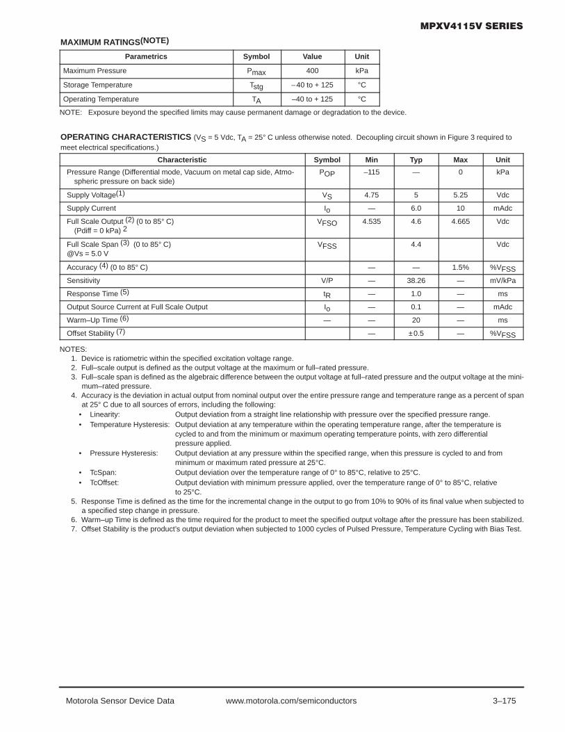
3–175Motorola Sensor Device Data www.motorola.com/semiconductors
MAXIMUM RATINGS(NOTE)
Parametrics Symbol Value Unit
Maximum Pressure Pmax 400 kPa
Storage Temperature Tstg –40 to + 125 °C
Operating Temperature TA –40 to + 125 °C
NOTE: Exposure beyond the specified limits may cause permanent damage or degradation to the device.
OPERATING CHARACTERISTICS (VS = 5 Vdc, TA = 25° C unless otherwise noted. Decoupling circuit shown in Figure 3 required tomeet electrical specifications.)
Characteristic Symbol Min Typ Max Unit
Pressure Range (Differential mode, Vacuum on metal cap side, Atmo-spheric pressure on back side)
POP –115 — 0 kPa
Supply Voltage(1) VS 4.75 5 5.25 Vdc
Supply Current Io — 6.0 10 mAdc
Full Scale Output (2) (0 to 85° C)(Pdiff = 0 kPa) 2
VFSO 4.535 4.6 4.665 Vdc
Full Scale Span (3) (0 to 85° C)@Vs = 5.0 V
VFSS 4.4 Vdc
Accuracy (4) (0 to 85° C) — — 1.5% %VFSS
Sensitivity V/P — 38.26 — mV/kPa
Response Time (5) tR — 1.0 — ms
Output Source Current at Full Scale Output Io — 0.1 — mAdc
Warm–Up Time (6) — — 20 — ms
Offset Stability (7) — ±0.5 — %VFSS
NOTES:1. Device is ratiometric within the specified excitation voltage range.2. Full–scale output is defined as the output voltage at the maximum or full–rated pressure.3. Full–scale span is defined as the algebraic difference between the output voltage at full–rated pressure and the output voltage at the mini-
mum–rated pressure.4. Accuracy is the deviation in actual output from nominal output over the entire pressure range and temperature range as a percent of span
at 25° C due to all sources of errors, including the following:• Linearity: Output deviation from a straight line relationship with pressure over the specified pressure range.• Temperature Hysteresis: Output deviation at any temperature within the operating temperature range, after the temperature is
cycled to and from the minimum or maximum operating temperature points, with zero differentialpressure applied.
• Pressure Hysteresis: Output deviation at any pressure within the specified range, when this pressure is cycled to and from minimum or maximum rated pressure at 25°C.
• TcSpan: Output deviation over the temperature range of 0° to 85°C, relative to 25°C.• TcOffset: Output deviation with minimum pressure applied, over the temperature range of 0° to 85°C, relative
to 25°C.5. Response Time is defined as the time for the incremental change in the output to go from 10% to 90% of its final value when subjected to
a specified step change in pressure.6. Warm–up Time is defined as the time required for the product to meet the specified output voltage after the pressure has been stabilized.7. Offset Stability is the product’s output deviation when subjected to 1000 cycles of Pulsed Pressure, Temperature Cycling with Bias Test.

3–176 Motorola Sensor Device Datawww.motorola.com/semiconductors
ON–CHIP TEMPERATURE COMPENSATION, CALIBRATION AND SIGNAL CONDITIONING
The performance over temperature is achieved by inte-grating the shear–stress strain gauge, temperature com-pensation, calibration and signal conditioning circuitry onto asingle monolithic chip.
Figure 2 illustrates the gauge configuration in the basic chipcarrier (Case 482). A fluorosilicone gel isolates the die surfaceand wire bonds from the environment, while allowing the pres-sure signal to be transmitted to the silicon diaphragm.
The MPXV4115V series sensor operating characteristicsare based on use of dry air as pressure media. Media, otherthan dry air, may have adverse effects on sensor performanceand long–term reliability. Internal reliability and qualificationtest for dry air, and other media, are available from the factory.Contact the factory for information regarding media tolerancein your application.
Figure 3 shows the recommended decoupling circuit forinterfacing the output of the integrated sensor to the A/D in-put of a microprocessor or microcontroller. Proper decoup-ling of the power supply is recommended.
Figure 4 shows the sensor output signal relative to differ-ential pressure input. Typical, minimum and maximum out-put curves are shown for operation over a temperature rangeof 0°C to 85°C using the decoupling circuit shown in Figure 3.The output will saturate outside of the specified pressurerange.
Figure 2. Cross–Sectional Diagram (Not to Scale)
1.0 F
IPS
470 pF
OUTPUT
Vs
5 V
0.01 F GND
Vout
Figure 3. Recommended power supply decouplingand output filtering.
For additional output filtering, please refer toApplication Note AN1646.
FLUOROSILICONEGEL DIE COAT
WIRE BOND
DIFFERENTIAL SENSINGELEMENT
THERMOPLASTICCASE
STAINLESSSTEEL CAP
LEADFRAME
P1
P2DIE BOND
DIE
Figure 4. Applied Vacuum in kPa (belowatmospheric pressure)
MAX
TRANSFER FUNCTION: Vout = VS*[(0.007652*P) + 0.92] ± (Pressure error*Temp Factor*0.007652*VS)VS = 5.0 V ± 0.25 VdcTEMP = 0–85° C
MIN
–115 –95 –75 –55 –35 –150
0.5
1
1.5
2
2.5
3
3.5
4
4.5
5
Vout vs. VACUUM
TRANSFER FUNCTION MPXV4115V
OU
TPU
T (V
OLT
S)

3–177Motorola Sensor Device Data www.motorola.com/semiconductors
ORDERING INFORMATION
The MPXV4115V series pressure sensors are available in the basic element package or with a pressure port. Two packingoptions are also offered.
Device Type Case No Packing Options Device MarkingDevice Type Case No. Packing Options Device Marking
MPXV4115V6U 482 Rails MPXV4115V
MPXV4115V6T1 482 Tape and Reel MPXV4115V
MPXV4115VC6U 482A Rails MPXV4115V
MINIMUM RECOMMENDED FOOTPRINT FOR SURFACE MOUNTED APPLICATIONS
Surface mount board layout is a critical portion of the totaldesign. The footprint for the surface mount packages mustbe the correct size to ensure proper solder connection inter-face between the board and the package. With the correct
fottprint, the packages will self align when subjected to asolder reflow process. It is always recommended to designboards with a solder mask layer to avoid bridging and short-ing between solder pads.
0.66016.76
0.060 TYP 8X1.52
0.100 TYP 8X2.54
0.100 TYP 8X2.54
0.3007.62
Figure 5. SOP Footprint (Case 482)
inchmm SCALE 2:1

3–178 Motorola Sensor Device Datawww.motorola.com/semiconductors
–85 –60 –45 –30 –15–115 –100 0
Transfer Function
Nominal Transfer Value: Vout = VS (P x 0.007652 ) 0.92)+/– (Pressure Error x Temp. Factor x 0.007652 x VS)VS = 5 V ± 0.25 Vdc
Temperature Error Band
Temp Multiplier
– 40 30 to 85 1+125 3
Temperature in C°
4.0
3.0
2.0
0.0
1.0
–40 –20 0 20 40 60 14012010080
MPXV4115V Series
TemperatureError
Factor
Pressure Error Band
Pressure in kPa(below atmospheric)
Pressure Error (Max)
1.950
1.725
1.500
–1.500
– 1.725
– 1.950
Pres
sure
Erro
r (kP
a)
NOTE: The Temperature Multiplier is a linear response from 0° to –40°C and from 85° to 125°C.
–115 to 0 kPa 1.725 (kPa)
0

3–179Motorola Sensor Device Data www.motorola.com/semiconductors
$"$ "##%" # "! $ !"$%" !#$ "$
The MPXV5004G series piezoresistive transducer is a state–of–the–art monolithicsilicon pressure sensor designed for a wide range of applications, but particularly thoseemploying a microcontroller or microprocessor with A/D inputs. This sensor combines ahighly sensitive implanted strain gauge with advanced micromachining techniques,thin–film metallization, and bipolar processing to provide an accurate, high level analogoutput signal that is proportional to the applied pressure.
Features
• Temperature Compensated over 10° to 60°C• Available in Gauge Surface Mount (SMT) or Through–
hole (DIP) Configurations
• Durable Thermoplastic (PPS) Package
Application Examples
• Washing Machine Water Level
• Ideally Suited for Microprocessor or Microcontroller–Based Systems
Figure 1. Fully Integrated Pressure SensorSchematic
VS
SENSINGELEMENT
Vout
GND
THIN FILMTEMPERATURECOMPENSATION
ANDGAIN STAGE #1
GAIN STAGE #2AND
GROUNDREFERENCE
SHIFT CIRCUITRY
PINS 1, 5, 6, 7, AND 8 ARE NO CONNECTSFOR SMALL OUTLINE PACKAGE DEVICE
SEMICONDUCTOR TECHNICAL DATA
PIN NUMBER
1
2
3
N/C
VSGnd
5
6
7
N/C
N/C
N/C
4 Vout 8 N/C
INTEGRATEDPRESSURE SENSOR
0 to 3.92 kPa(0 to 400 mm H 2O)
1.0 to 4.9 V OUTPUT
MPXV5004GC7UCASE 482C
SMALL OUTLINE PACKAGETHROUGH–HOLE
MPXV5004G7UCASE 482B
J
MPXV5004G6UCASE 482
MPXV5004GC6UCASE 482A
NOTE: Pins 1, 5, 6, 7, and 8 areinternal device connections. Do notconnect to external circuitry orground. Pin 1 is noted by the notch inthe lead.
SMALL OUTLINE PACKAGESURFACE MOUNT
MPXV5004DPCASE 1351
MPXV5004GVPCASE 1368
MPXV5004GPCASE 1369
REV 5
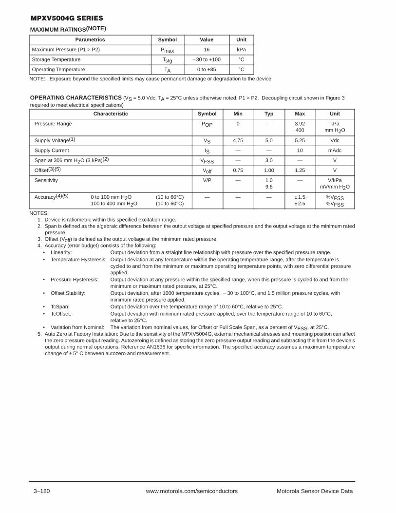
3–180 Motorola Sensor Device Datawww.motorola.com/semiconductors
MAXIMUM RATINGS(NOTE)
Parametrics Symbol Value Unit
Maximum Pressure (P1 > P2) Pmax 16 kPa
Storage Temperature Tstg –30 to +100 °C
Operating Temperature TA 0 to +85 °C
NOTE: Exposure beyond the specified limits may cause permanent damage or degradation to the device.
OPERATING CHARACTERISTICS (VS = 5.0 Vdc, TA = 25°C unless otherwise noted, P1 > P2. Decoupling circuit shown in Figure 3required to meet electrical specifications)
Characteristic Symbol Min Typ Max Unit
Pressure Range POP 0 — 3.92400
kPamm H2O
Supply Voltage(1) VS 4.75 5.0 5.25 Vdc
Supply Current IS — — 10 mAdc
Span at 306 mm H2O (3 kPa)(2) VFSS — 3.0 — V
Offset(3)(5) Voff 0.75 1.00 1.25 V
Sensitivity V/P — 1.09.8
— V/kPamV/mm H2O
Accuracy(4)(5) 0 to 100 mm H2O (10 to 60°C)100 to 400 mm H2O (10 to 60°C)
— — — ±1.5±2.5
%VFSS%VFSS
NOTES:1. Device is ratiometric within this specified excitation range.2. Span is defined as the algebraic difference between the output voltage at specified pressure and the output voltage at the minimum rated
pressure.3. Offset (Voff) is defined as the output voltage at the minimum rated pressure.4. Accuracy (error budget) consists of the following:
• Linearity: Output deviation from a straight line relationship with pressure over the specified pressure range.• Temperature Hysteresis: Output deviation at any temperature within the operating temperature range, after the temperature is
cycled to and from the minimum or maximum operating temperature points, with zero differential pressureapplied.
• Pressure Hysteresis: Output deviation at any pressure within the specified range, when this pressure is cycled to and from theminimum or maximum rated pressure, at 25°C.
• Offset Stability: Output deviation, after 1000 temperature cycles, 30 to 100°C, and 1.5 million pressure cycles, withminimum rated pressure applied.
• TcSpan: Output deviation over the temperature range of 10 to 60°C, relative to 25°C.• TcOffset: Output deviation with minimum rated pressure applied, over the temperature range of 10 to 60°C,
relative to 25°C.• Variation from Nominal: The variation from nominal values, for Offset or Full Scale Span, as a percent of VFSS, at 25°C.
5. Auto Zero at Factory Installation: Due to the sensitivity of the MPXV5004G, external mechanical stresses and mounting position can affectthe zero pressure output reading. Autozeroing is defined as storing the zero pressure output reading and subtracting this from the device’soutput during normal operations. Reference AN1636 for specific information. The specified accuracy assumes a maximum temperaturechange of ± 5° C between autozero and measurement.

3–181Motorola Sensor Device Data www.motorola.com/semiconductors
ON–CHIP TEMPERATURE COMPENSATION, CALIBRATION AND SIGNAL CONDITIONING
The performance over temperature is achieved by inte-grating the shear–stress strain gauge, temperature com-pensation, calibration and signal conditioning circuitry onto asingle monolithic chip.
Figure 2 illustrates the gauge configuration in the basic chipcarrier (Case 482). A fluorosilicone gel isolates the die surfaceand wire bonds from the environment, while allowing the pres-sure signal to be transmitted to the silicon diaphragm.
The MPXV5004G series sensor operating characteristicsare based on use of dry air as pressure media. Media, otherthan dry air, may have adverse effects on sensor performanceand long–term reliability. Internal reliability and qualification
test for dry air, and other media, are available from the factory.Contact the factory for information regarding media tolerancein your application.
Figure 3 shows the recommended decoupling circuit for in-terfacing the output of the MPXV5004G to the A/D input ofthe microprocessor or microcontroller. Proper decoupling ofthe power supply is recommended.
Figure 4 shows the sensor output signal relative to pres-sure input. Typical, minimum and maximum output curvesare shown for operation over a temperature range of 10°C to60°C using the decoupling circuit shown in Figure 3. Theoutput will saturate outside of the specified pressure range.
Figure 2. Cross–Sectional Diagram (Not to Scale)
1.0 F
IPS
470 pF
OUTPUT
Vs
5 V
0.01 F GND
Vout
Figure 3. Recommended power supply decouplingand output filtering.
For additional output filtering, please refer toApplication Note AN1646.
FLUOROSILICONEGEL DIE COAT
WIRE BOND
DIFFERENTIAL SENSINGELEMENT
THERMOPLASTICCASE
STAINLESSSTEEL CAP
LEADFRAME
P1
P2DIE BOND
DIE
Figure 4. Output versus Pressure Differential
MAX
DIFFERENTIAL PRESSURE
5.0
4.0
3.0
2.0
OU
TPU
T (V
)
TRANSFER FUNCTION: Vout = VS*[(0.2*P) + 0.2] ± 1.5% VFSSVS = 5.0 V ± 0.25 VdcTEMP = 10 to 60°C
1.0
MIN
TYPICAL
2 kPa200 mm H2O
(See Note 5 in Operating Characteristics)
4 kPa400 mm H2O

3–182 Motorola Sensor Device Datawww.motorola.com/semiconductors
PRESSURE (P1)/VACUUM (P2) SIDE IDENTIFICATION TABLE
Motorola designates the two sides of the pressure sensoras the Pressure (P1) side and the Vacuum (P2) side. ThePressure (P1) side is the side containing silicone gel whichisolates the die from the environment. The Motorola pressure
sensor is designed to operate with positive differential pres-sure applied, P1 > P2.
The Pressure (P1) side may be identified by using the tablebelow:
Part Number Case Type Pressure (P1) Side Identifier
MPXV5004GC6U/T1 482A Side with Port Attached
MPXV5004G6U/T1 482 Stainless Steel Cap
MPXV5004GC7U 482C Side with Port Attached
MPXV5004G7U 482B Stainless Steel Cap
MPXV5004GP 1369 Side with Port Attached
MPXV5004DP 1351 Side with Port Marking
MPXV5004GVP 1368 Stainless Steel Cap
ORDERING INFORMATION
MPXV5004G series pressure sensors are available in the basic element package or with a pressure port. Two packingoptions are offered for the surface mount configuration.
Device Type / Order No Case No Packing Options Device MarkingDevice Type / Order No. Case No. Packing Options Device Marking
MPXV5004G6U 482 Rails MPXV5004G
MPXV5004G6T1 482 Tape and Reel MPXV5004G
MPXV5004GC6U 482A Rails MPXV5004G
MPXV5004GC6T1 482A Tape and Reel MPXV5004G
MPXV5004GC7U 482C Rails MPXV5004G
MPXV5004G7U 482B Rails MPXV5004G
MPXV5004GP 1369 Trays MPXV5004G
MPXV5004DP 1351 Trays MPXV5004G
MPXV5004GVP 1368 Trays MPXV5004G
INFORMATION FOR USING THE SMALL OUTLINE PACKAGE (CASE 482)
MINIMUM RECOMMENDED FOOTPRINT FOR SURFACE MOUNTED APPLICATIONS
Surface mount board layout is a critical portion of the totaldesign. The footprint for the surface mount packages mustbe the correct size to ensure proper solder connection inter-face between the board and the package. With the correct
fottprint, the packages will self align when subjected to asolder reflow process. It is always recommended to designboards with a solder mask layer to avoid bridging and short-ing between solder pads.
0.66016.76
0.060 TYP 8X1.52
0.100 TYP 8X2.54
0.100 TYP 8X2.54
0.3007.62
Figure 5. SOP Footprint (Case 482)
inchmm SCALE 2:1

3–183Motorola Sensor Device Data www.motorola.com/semiconductors
!"$%" %"&$"$ "##%" # " ! $ !"$%" !#$ "$
Motorola’s MPXV6115VC6U sensor integrates on–chip, bipolar op ampcircuitry and thin film resistor networks to provide a high output signal andtemperature compensation. The small form factor and high reliability of on–chipintegration make the Motorola pressure sensor a logical and economical choicefor the system designer.
The MPXV6115VC6U piezoresistive transducer is a state–of–the–art,monolithic, signal conditioned, silicon pressure sensor. This sensor combinesadvanced micromachining techniques, thin film metallization, and bipolar semi-conductor processing to provide an accurate, high level analog output signal that isproportional to applied pressure.
Figure 1 shows a block diagram of the internal circuitry integrated on apressure sensor chip.
Features
• Improved Accuracy at High Temperature
• 1.5% Maximum Error over 0° to 85°C• Ideally suited for Microprocessor or Microcontroller–Based Systems
• Temperature Compensated from –40° to +125°C• Durable Thermoplastic (PPS) Surface Mount Package
Application Examples
• Vacuum Pump Monitoring
• Brake Booster Monitoring
Figure 1. Fully Integrated Pressure SensorSchematic
VS
SENSINGELEMENT
Vout
GND
THIN FILMTEMPERATURECOMPENSATION
ANDGAIN STAGE #1
GAIN STAGE #2AND
GROUNDREFERENCE
SHIFT CIRCUITRY
PINS 1, 5, 6, 7 AND 8 ARE NO CONNECTS
SEMICONDUCTOR TECHNICAL DATA
5
6
7
8
N/C
VSGnd
Vout
N/C
N/C
N/C
INTEGRATEDPRESSURE SENSOR
–115 to 0 kPa (–16.7 to 2.2 psi)0.2 to 4.6 Volts Output
PIN NUMBER
NOTE: Pins 1, 5, 6, 7, and 8 are internal deviceconnections. Do not connect to external circuitryor ground. Pin 1 is denoted by the notch in thelead.
1
2
3
MPXV6115VC6UCASE 482A
4 N/C
SMALL OUTLINE PACKAGE
REV 0
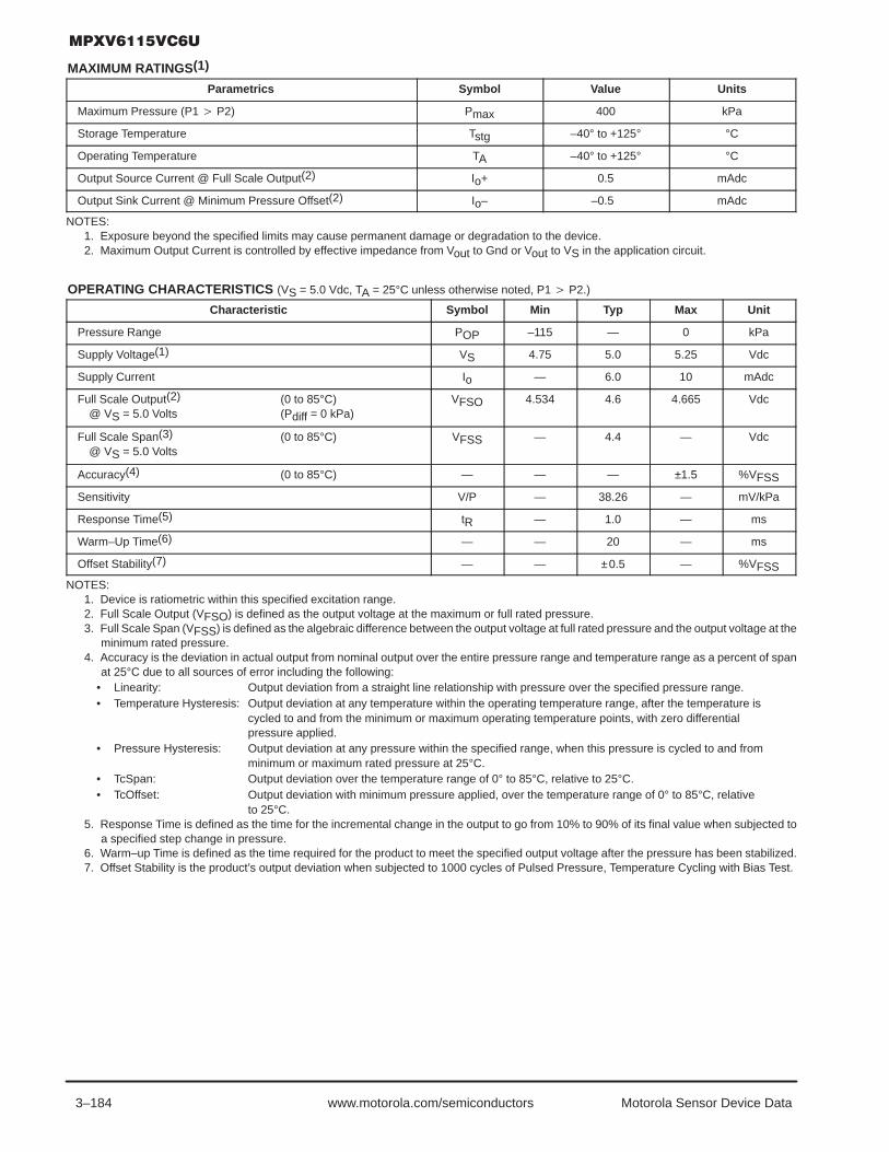
3–184 Motorola Sensor Device Datawww.motorola.com/semiconductors
MAXIMUM RATINGS(1)
Parametrics Symbol Value Units
Maximum Pressure (P1 P2) Pmax 400 kPa
Storage Temperature Tstg –40° to +125° °C
Operating Temperature TA –40° to +125° °C
Output Source Current @ Full Scale Output(2) Io+ 0.5 mAdc
Output Sink Current @ Minimum Pressure Offset(2) Io– –0.5 mAdc
NOTES:1. Exposure beyond the specified limits may cause permanent damage or degradation to the device.2. Maximum Output Current is controlled by effective impedance from Vout to Gnd or Vout to VS in the application circuit.
OPERATING CHARACTERISTICS (VS = 5.0 Vdc, TA = 25°C unless otherwise noted, P1 P2.)
Characteristic Symbol Min Typ Max Unit
Pressure Range POP –115 — 0 kPa
Supply Voltage(1) VS 4.75 5.0 5.25 Vdc
Supply Current Io — 6.0 10 mAdc
Full Scale Output(2) (0 to 85°C)@ VS = 5.0 Volts (Pdiff = 0 kPa)
VFSO 4.534 4.6 4.665 Vdc
Full Scale Span(3) (0 to 85°C)@ VS = 5.0 Volts
VFSS — 4.4 — Vdc
Accuracy(4) (0 to 85°C) — — — ±1.5 %VFSS
Sensitivity V/P — 38.26 — mV/kPa
Response Time(5) tR — 1.0 — ms
Warm–Up Time(6) — — 20 — ms
Offset Stability(7) — — ±0.5 — %VFSS
NOTES:1. Device is ratiometric within this specified excitation range.2. Full Scale Output (VFSO) is defined as the output voltage at the maximum or full rated pressure.3. Full Scale Span (VFSS) is defined as the algebraic difference between the output voltage at full rated pressure and the output voltage at the
minimum rated pressure.4. Accuracy is the deviation in actual output from nominal output over the entire pressure range and temperature range as a percent of span
at 25°C due to all sources of error including the following:• Linearity: Output deviation from a straight line relationship with pressure over the specified pressure range.• Temperature Hysteresis: Output deviation at any temperature within the operating temperature range, after the temperature is
cycled to and from the minimum or maximum operating temperature points, with zero differentialpressure applied.
• Pressure Hysteresis: Output deviation at any pressure within the specified range, when this pressure is cycled to and from minimum or maximum rated pressure at 25°C.
• TcSpan: Output deviation over the temperature range of 0° to 85°C, relative to 25°C.• TcOffset: Output deviation with minimum pressure applied, over the temperature range of 0° to 85°C, relative
to 25°C.5. Response Time is defined as the time for the incremental change in the output to go from 10% to 90% of its final value when subjected to
a specified step change in pressure.6. Warm–up Time is defined as the time required for the product to meet the specified output voltage after the pressure has been stabilized.7. Offset Stability is the product’s output deviation when subjected to 1000 cycles of Pulsed Pressure, Temperature Cycling with Bias Test.
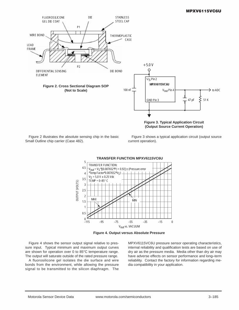
3–185Motorola Sensor Device Data www.motorola.com/semiconductors
Figure 2. Cross Sectional Diagram SOP(Not to Scale)
Figure 3. Typical Application Circuit(Output Source Current Operation)
VS Pin 2
5.0 V
GND Pin 3
Vout Pin 4
MPXV6115VC6U
to ADC100 nF
51 K47 pF
FLUOROSILICONEGEL DIE COAT
WIRE BOND
DIFFERENTIAL SENSINGELEMENT
THERMOPLASTICCASE
STAINLESSSTEEL CAP
LEADFRAME
P1
P2DIE BOND
DIE
Figure 2 illustrates the absolute sensing chip in the basicSmall Outline chip carrier (Case 482).
Figure 3 shows a typical application circuit (output sourcecurrent operation).
Figure 4. Output versus Absolute Pressure
MAX
TRANSFER FUNCTION: Vout = VS*[(0.007652*P) + 0.92] ± (Pressure error*Temp Factor*0.007652*VS)VS = 5.0 V ± 0.25 VdcTEMP = 0–85° C
MIN
–115 –95 –75 –55 –35 –150
0.5
1
1.5
2
2.5
3
3.5
4
4.5
5
Vout vs. VACUUM
TRANSFER FUNCTION MPXV6115VC6U
OU
TPU
T (V
OLT
S)
0
Figure 4 shows the sensor output signal relative to pres-sure input. Typical minimum and maximum output curvesare shown for operation over 0 to 85°C temperature range.The output will saturate outside of the rated pressure range.
A fluorosilicone gel isolates the die surface and wirebonds from the environment, while allowing the pressuresignal to be transmitted to the silicon diaphragm. The
MPXV6115VC6U pressure sensor operating characteristics,internal reliability and qualification tests are based on use ofdry air as the pressure media. Media other than dry air mayhave adverse effects on sensor performance and long–termreliability. Contact the factory for information regarding me-dia compatibility in your application.

3–186 Motorola Sensor Device Datawww.motorola.com/semiconductors
Transfer Function (MPXV6115VC6U)
Nominal Transfer Value: Vout = VS x (0.007652 x P + 0.92)± (Pressure Error x Temp. Factor x 0.007652 x VS)VS = 5.0 ± 0.25 Vdc
Temperature Error BandMPXV6115VC6U
Break Points
Temp Multiplier
– 40 30 to 85 1125 2
Temperature in C°
4.0
3.0
2.0
0.0
1.0
–40 –20 0 20 40 60 14012010080
TemperatureError
Factor
NOTE: The Temperature Multiplier is a linear response from 0°C to –40°C and from 85°C to 125°C
Pressure Error Band
–85 –60 –45 –30 –15–115 –100 0Pressure in kPa(below atmospheric)
Pressure Error (Max)
1.950
1.725
1.500
–1.500
– 1.725
– 1.950
Pres
sure
Erro
r (kP
a)
–115 to 0 kPa 1.725 (kPa)
0
Error Limits for Pressure
ORDERING INFORMATION — SMALL OUTLINE PACKAGE
Device Type Options Case No. MPX Series Order No. Packing Options Marking
Ported Element Vacuum, Axial Port 482A MPXV6115VC6U Rails MPXV6115V

3–187Motorola Sensor Device Data www.motorola.com/semiconductors
SURFACE MOUNTING INFORMATION
MINIMUM RECOMMENDED FOOTPRINT FOR SMALL OUTLINE PACKAGE
Surface mount board layout is a critical portion of the totaldesign. The footprint for the semiconductor package mustbe the correct size to ensure proper solder connection inter-face between the board and the package. With the correctpad geometry, the packages will self–align when subjected to
a solder reflow process. It is always recommended to fabri-cate boards with a solder mask layer to avoid bridging and/orshorting between solder pads, especially on tight tolerancesand/or tight layouts.
0.66016.76
0.060 TYP 8X1.52
0.100 TYP 8X2.54
0.100 TYP2.54
0.3007.62
Figure 5. SOP Footprint (Case 482A)
inchmm

3–188 Motorola Sensor Device Datawww.motorola.com/semiconductors
! !# ! " "
Prepared by: Carl DemingtonDesign Engineering
INTRODUCTION
This application note describes a technique to improve thelinearity of Motorola’s MPX10 series (i.e., MPX10, MPXV10,and MPX12 pressure sensors) pressure transducers whenthey are interfaced to a microprocessor system. Thelinearization technique allows the user to obtain both highsensitivity and good linearity in a cost effective system.
The MPX10, MPXV10 and MPX12 pressure transducersare semiconductor devices which give an electrical outputsignal proportional to the applied pressure over the pressurerange of 0–10 kPa (0–75 mm Hg). These devices use a uniquetransverse voltage–diffused silicon strain–gauge which issensitive to stress produced by pressure applied to a thinsilicon diaphragm.
One of the primary considerations when using a pressuretransducer is the linearity of the transfer function, since thisparameter has a direct effect on the total accuracy of thesystem, and compensating for nonlinearities with peripheralcircuits is extremely complicated and expensive. The purposeof this document is to outline the causes of nonlinearity, thetrade–offs that can be made for increased system accuracy,and a relatively simple technique that can be utilized tomaintain system performance, as well as system accuracy.
ORIGINS OF NONLINEARITY
Nonlinearity in semiconductor strain–gauges is a topic thathas been the target of many experiments and muchdiscussion. Parameters such as resistor size and orientation,surface impurity levels, oxide passivation thickness andgrowth temperatures, diaphragm size and thickness are allcontributors to nonlinear behavior in silicon pressuretransducers. The Motorola X–ducer was designed to minimizethese effects. This goal was certainly accomplished in theMPX2000 series which have a maximum nonlinearity of 0.1%FS. However, to obtain the higher sensitivity of the MPX10series, a maximum nonlinearity of ±1% FS has to be allowed.The primary cause of the additional nonlinearity in the MPX10series is due to the stress induced in the diaphragm by appliedpressure being no longer linear.
One of the basic assumptions in using semiconductorstrain–gauges as pressure sensors is that the deflection of thediaphragm when pressure is applied is small compared to thethickness of the diaphragm. With devices that are verysensitive in the low pressure ranges, this assumption is nolonger valid. The deflection of the diaphragm is a considerablepercentage of the diaphragm thickness, especially in deviceswith higher sensitivities (thinner diaphragms). The resultingstresses do not vary linearly with applied pressure. Thisbehavior can be reduced somewhat by increasing the area ofthe diaphragm and consequently thickening the diaphragm.Due to the constraint, the device is required to have highsensitivity over a fairly small pressure range, and thenonlinearity cannot be eliminated. Much care was given in thedesign of the MPX10 series to minimize the nonlinearbehavior. However, for systems which require greateraccuracy, external techniques must be used to account for thisbehavior.
PERFORMANCE OF AN MPX DEVICE
The output versus pressure of a typical MPX12 along withan end–point straight line is shown in Figure 1. All nonlinearityerrors are referenced to the end–point straight line (see datasheet). Notice there is an appreciable deviation from theend–point straight line at midscale pressure. This shape ofcurve is consistent with MPX10 and MPXV10, as well asMPX12 devices, with the differences between the parts beingthe magnitude of the deviation from the end–point line. Themajor tradeoff that can be made in the total deviceperformance is sensitivity versus linearity.
Figure 2 shows the relationship between full scale span andnonlinearity error for the MPX10 series of devices. The datashows the primary contribution to nonlinearity isnonproportional stress with pressure, while assembly andpackaging stress (scatter of the data about the line) is fairlysmall and well controlled. It can be seen that relatively goodaccuracies (<0.5% FS) can be achieved at the expense ofreduced sensitivity, and for high sensitivity the nonlinearityerrors increase rapidly. The data shown in Figure 2 was takenat room temperature with a constant voltage excitation of3.0 volts.
SEMICONDUCTOR APPLICATION NOTE
REV 3

3–189Motorola Sensor Device Data www.motorola.com/semiconductors
90
80
70
60
50
40
30
20
10
09080706050403020100
PRESSURE (torr)
Figure 1. MPX12 Linearity Analysis Raw Data
V out
(mV)
5.0
100
SPAN (mV)
Figure 2. MPX10 Series Span versus Linearity
LIN
EAR
ITY
(% F
S)
4.0
3.0
2.0
1.0
0
–1.09080706050403020
COMPENSATION FOR NONLINEARITYThe nonlinearity error shown in Figure 1 arises from the
assumption that the output voltage changes with respect topressure in the following manner:
Vout = Voff + sens*P [1]where Voff = output voltage at zero pressure
differentialsens = sensitivity of the device
P = applied pressure
It is obvious that the true output does not follow this simplestraight line equation. Therefore, if an expression could bedetermined with additional higher order terms that moreclosely described the output behavior, increased accuracieswould be possible. The output expression would then become
Vout = Voff +(B0+B1*P+B2*P2+B3*P3 +. . .) [2]
where B0, B1, B2, B3, etc. are sensitivity coefficients. Inorder to determine the sensitivity coefficients given in equation[2] for the MPX10 series of pressure transducers, a polynomialregression analysis was performed on data taken from 139devices with full scale spans ranging from 30 to 730 mV. It wasfound that second order terms are sufficient to give excellentagreement with experimental data. The calculated regressioncoefficients were typically 0.999999+ with the worst casebeing 0.99999. However, these sensitivity coefficientsdemonstrated a strong correlation with the full scale span ofthe device for which they were calculated. The correlation ofB0, B1, and B2 with full scale span is shown in Figures 3through 5.
0.5
25
SPAN (mV)
B
45 7055 6050403020
0.4
0.30.20.1
0– 0.1– 0.2
– 0.3– 0.4– 0.5
35 65
0
Figure 3. MPX10 Linearity Analysis —Correlation of B 0 Vout = B0 + B1 (P) + B2 (P)2
B0 = 0.1045 – 0.00295*(SPAN)
1.1
25
SPAN (mV)
B45 7055 6050403020 35 65
1
Figure 4. MPX10 Linearity Analysis —Correlation of B 1 Vout = B0 + B1 (P) + B2 (P)2
1.0
0.9
0.8
0.7
0.6
0.5
0.4
0.30.2
B1 = 0.2055 + 1.598E – 3*(SPAN)+ 1.723E – 4*(SPAN)2
0.0030
25
SPAN (mV)
–B
45 7055 6050403020 35 65
2
Figure 5. MPX10 Linearity Analysis —Correlation of B 2 Vout = B0 + B1 (P) + B2 (P)2
0.0025
0.0020
0.0015
0.0010
0.0005
B2 = –1.293E – 13*(SPAN)5.68
In order to simplify the determination of these coefficientsfor the user, further regression analysis was performed so thatexpressions could be given for each coefficient as a functionof full scale span. This would then allow the user to do a singlepressure measurement, a series of calculations, andanalytically arrive at the equation of the line that describes theoutput behavior of the transducer. Nonlinearity errors werethen calculated by comparing experimental data with thevalues calculated using equation [2] and the sensitivitycoefficients given by the regression analysis. The resultingerrors are shown in Figures 6 through 9 at various pressurepoints. While using this technique has been successful inreducing the errors due to nonlinearity, the considerablespread and large number of devices that showed errors >1%indicate this technique was not as successful as desired.

3–190 Motorola Sensor Device Datawww.motorola.com/semiconductors
Figure 6. Linearity Error of General Fit Equation at 1/4 FS
Figure 7. Linearity Error of General Fit Equation at 1/2 FS
30
27
24
21
18
15
12
9.0
6.0
3.0
0.0
21.54
19.38
17.23
15.08
12.92
10.77
8.62
6.46
4.31
2.15
– 2.0 –1.8 –1.6 –1.4 –1.2 –1.0 – 0.8 – 0.6 – 0.4 – 0.2 0.0 0.2 0.4 0.6 0.8 1.0 1.2 1.4 1.6 1.8 2.0
NO. OF UNITS
LINEARITY ERROR (% FS)
General FitP = 1/4 FS
Average Error = 0.15Standard Deviation = 0.212
NO. OF UNITSLINEARITY ERROR (% FS)
General FitP = 1/2 FS
Average Error = – 0.02Standard Deviation = 0.391
16.15
14.54
12.92
11.31
9.69
8.08
6.46
4.85
3.23
1.62
21
18
15
12
9.0
6.0
3.0
0.0– 2.0 –1.8 –1.6 –1.4 –1.2 –1.0 – 0.8 – 0.6 – 0.4 – 0.2 0.0 0.2 0.4 0.6 0.8 1.0 1.2 1.4 1.6 1.8 2.0
%
%

3–191Motorola Sensor Device Data www.motorola.com/semiconductors
Figure 8. Linearity Error of General Fit Equation at 3/4 FS
Figure 9. Linearity Error of General Fit Equation at FS
16.5
0.0
12.31
11.08
9.85
8.62
7.38
6.15
4.92
3.69
2.46
1.23
– 2.0 –1.8 –1.6 –1.4 –1.2 –1.0 – 0.8 – 0.6 – 0.4 – 0.2 0.0 0.2 0.4 0.6 0.8 1.0 1.2 1.4 1.6 1.8 2.0
NO. OF UNITSLINEARITY ERROR (% FS)
General FitP = 3/4 FS
Average Error = – 0.10Standard Deviation = 0.549
%
15
13.5
12
10.5
9.0
7.5
6.0
4.5
3.0
1.5
19.5
0.0
13.85
12.46
11.08
9.69
8.31
6.92
5.54
4.15
2.77
1.38
– 2.0 –1.6 –1.4 –1.2 –1.0 – 0.8 – 0.6 – 0.4 – 0.2 0.0 0.2 0.4 0.6 0.8 1.0 1.2 1.4 1.6 1.8 2.0
NO. OF UNITS
LINEARITY ERROR (% FS)
General FitP = 1 FS
Average Error = 0.11Standard Deviation = 0.809
%
18
16.5
15
13.5
12
10.5
6.0
4.5
3.0
1.5
9.0
7.5
–1.8

3–192 Motorola Sensor Device Datawww.motorola.com/semiconductors
A second technique that still uses a single pressuremeasurement as the input was investigated. In this method,the sensitivity coefficients are calculated using a piece–wiselinearization technique where the total span variation isdivided into four windows of 10 mV (i.e., 30–39.99, 40–49.99,etc.) and coefficients calculated for each window. The errorsthat arise out of using this method are shown in Figures 10through 13. This method results in a large majority of the
devices having errors <0.5%, while only one of the deviceswas >1%. The sensitivity coefficients that are substituted intoequation [2] for the different techniques are given in Table 1.It is important to note that for either technique the onlymeasurement that is required by the user in order to clearlydetermine the sensitivity coefficients is the determination ofthe full scale span of the particular pressure transducer.
Figure 10. Linearity Error of Piece–Wise Linear Fit at 1/4 FS
48
42
36
30
24
18
12
6.0
0.0
37.69
33.92
30.15
26.38
22.62
18.85
15.08
11.31
7.54
3.77
– 2.0 –1.6 –1.4 –1.2 –1.0 – 0.8 – 0.6 – 0.4 – 0.2 0.0 0.2 0.4 0.6 0.8 1.0 1.2 1.4 1.6 1.8 2.0
NO. OF UNITSLINEARITY ERROR (% FS)
General FitP = 1/4 FS
Average Error = 0.18Standard Deviation = 0.159
%
–1.8
Table 1. Comparison of Linearization Methods
SPAN WINDOW B0 B1 B2
GENERAL FIT
0.1045 + 2.95E – 3X 0.2055 + 1.598E – 3X + 1.723E – 4X2 1.293E – 13X5.681
PIECE–WISE LINEAR FIT
30–39.99 0.08209 – 2.246E – 3X 0.02433 = 1.430E – 2X –1.961E – 4 + 8.816E – 6X
40–49.99 0.1803 – 4.67E – 3X –0.119 + 1.655E – 2X –1.572E – 3 + 4.247E – 5X
50–59.99 0.1055 – 3.051E – 3X –0.355 + 2.126E – 2X –5.0813 – 3 + 1.116E – 4X
60–69.99 –0.288 + 3.473E – 3X –0.361 + 2.145E – 2X –5.928E – 3 + 1.259E – 4X
X = Full Scale Span

3–193Motorola Sensor Device Data www.motorola.com/semiconductors
Figure 11. Linearity Error of Piece–Wise Linear Fit at 1/2 FS
Figure 12. Linearity Error of Piece–Wise Linear Fit at 3/4 PS
27
24
21
18
15
12
9.0
6.0
0.0
20
18
16
14
12
10
8.0
6.0
4.0
2.0
– 2.0 –1.6 –1.4 –1.2 –1.0 – 0.8 – 0.6 – 0.4 – 0.2 0.0 0.2 0.4 0.6 0.8 1.0 1.2 1.4 1.6 1.8 2.0
NO. OF UNITS
LINEARITY ERROR (% FS)
General FitP = 1/2 FS
Average Error = 0.02Standard Deviation = 0.267
%
–1.8
3.0
21
18
15
12
9.0
6.0
0.0
16.15
14.54
12.92
11.31
9.69
8.08
6.46
4.85
3.23
1.62
– 2.0 –1.6 –1.4 –1.2 –1.0 – 0.8 – 0.6 – 0.4 – 0.2 0.0 0.2 0.4 0.6 0.8 1.0 1.2 1.4 1.6 1.8 2.0
NO. OF UNITS
LINEARITY ERROR (% FS)
General FitP = 3/4 FS
Average Error = – 0.09Standard Deviation = 0.257
%
–1.8
3.0

3–194 Motorola Sensor Device Datawww.motorola.com/semiconductors
Figure 13. Linearity Error of Piece–Wise Linear Fit at FS
52.5
45
37.5
30
22.5
15
7.5
0.0
38.46
34.62
30.77
26.92
23.08
19.23
15.38
11.54
7.69
3.85
– 2.0 –1.6 –1.4 –1.2 –1.0 – 0.8 – 0.6 – 0.4 – 0.2 0.0 0.2 0.4 0.6 0.8 1.0 1.2 1.4 1.6 1.8 2.0
NO. OF UNITSLINEARITY ERROR (% FS)
General FitP = 1 FS
Average Error = 0.13Standard Deviation = 0.186
%
–1.8
Once the sensitivity coefficients have been determined, asystem can then be built that provides an accurate outputfunction with pressure. The system shown in Figure 14consists of a pressure transducer, a temperaturecompensation and amplification stage, an A/D converter, amicroprocessor, and a display. The display block can bereplaced with a control function if required. The A/D convertersimply transforms the voltage signal to an input signal for themicroprocessor, in which resides the look–up table of thetransfer function generated from the previously determinedsensitivity coefficients. The microprocessor can then drive adisplay or control circuit using standard techniques.
SUMMARY
While at first glance this technique appears to be fairlycomplicated, it can be a very cost effective method of buildinga high–accuracy, high–sensitivity pressure–monitoringsystem for low–pressure ranges.
Figure 14. Linearization System Block Diagram
X–DUCER
TEMPERATURECOMPENSATIONAND AMPLIFICATION
MICROCONTROLLERMC68HC908QT4
DISPLAY

3–195Motorola Sensor Device Data www.motorola.com/semiconductors
"! " ! ! "
Prepared by: Randy FrankMotorola Inc., Semiconductor Products SectorPhoenix, Arizona
INTRODUCTIONMotorola’s MPX series pressure sensors are silicon
piezoresistive strain–gauges offered in a chip–carrierpackage (see Figure 1). The exclusive chip–carrier packagewas developed to realize the advantages of high–speed,automated assembly and testing. In addition to high volumeavailability and low cost, the chip–carrier package offers usersa number of packaging options. This Application Notedescribes several mounting techniques, offers lead formingrecommendations, and suggests means of testing the MPXseries of pressure sensors.
Figure 1. MPX Pressure Sensor In Chip CarrierPackage Shown with Port Options
DIFFERENTIALPORT OPTIONCASE 344C–01
Figure 2. Chip Carrier and Available Ported Packages
BASIC ELEMENTCASE 344–15SUFFIX A / D
GAUGE PORTCASE 344B–01SUFFIX AP / GP
GAUGE VACUUM PORTCASE 344D–01
SUFFIX GVP
DUAL PORTCASE 344C–01
SUFFIX DP
AXIAL PORTCASE 344F–01
SUFFIX ASX / GSX
AXIAL VACUUM PORTCASE 344G–01SUFFIX GVSX
STOVEPIPE PORTCASE 344A–01
SUFFIX GVS
STOVEPIPE VACUUM PORTCASE 344E–01SUFFIX AS/GS
BASIC ELEMENTCASE 867–08SUFFIX A / D
GAUGE PORTCASE 867B–04SUFFIX AP / GP
GAUGE VACUUM PORTCASE 867D–04
SUFFIX GVP
DUAL PORTCASE 867C–05
SUFFIX DP
AXIAL PORTCASE 867F–03
SUFFIX ASX / GSX
AXIAL VACUUM PORTCASE 867G–03SUFFIX GVSX
STOVEPIPE PORTCASE 867E–03SUFFIX AS / GS
STOVEPIPE VACUUM PORTCASE 867A–04
SUFFIX GVS
SEMICONDUCTOR APPLICATION NOTE
REV 3

3–196 Motorola Sensor Device Datawww.motorola.com/semiconductors
PORT ADAPTERS
Available PackagesMotorola’s chip–carrier package and available ports for
attachment of 1/8″ I.D. hose are made from a hightemperature thermoplastic that can withstand temperatureextremes from –50 to 150°C (see Figure 2). The port adapterswere designed for rivet or 5/32″ screw attachment to panels,printed circuit boards or chassis mounting.
Custom Port Adaptor Installation TechniquesThe Motorola MPX silicon pressure sensor is available in a
basic chip carrier cell which is adaptable for attachment tocustomer specific housings/ports (Case 344 for 4–pin devicesand Case 867 for 6–pin devices). The basic cell haschamfered shoulders on both sides which will accept anO–ring such as Parker Seal’s silicone O–ring(p/n#2–015–S–469–40). Refer to Figure 3 for therecommended O–ring to sensor cell interface dimensions.
The sensor cell may also be glued directly to a customhousing or port using many commercial grade epoxies or RTVadhesives which adhere to grade Valox 420, 30% glassreinforced polyester resin plastic or Union Carbide’s Udelpolysulfone (MPX2300DT1 only). Motorola recommendsusing Thermoset EP530 epoxy or an equivalent. The epoxyshould be dispensed in a continuous bead around thecase–to–port interface shoulder. Refer to Figure 4. Care mustbe taken to avoid gaps or voids in the adhesive bead to helpensure that a complete seal is made when the cell is joined tothe port. The recommended cure conditions for ThermosetEP539 are 15 minutes at 150°C. After cure, a simple test forgross leaks should be performed to ensure the integrity of the
cell to port bond. Submerging the device in water for 5seconds with full rated pressure applied to the port nozzle andchecking for air bubbles will provide a good indication.
TESTING MPX SERIES PRESSURE SENSORS
Pressure ConnectionTesting of pressure sensing elements in the chip carrier
package can be performed easily by using a clamping fixturewhich has an O–ring seal to attach to the beveled surface.Figure 8 shows a diagram of the fixture that Motorola uses toapply pressure or vacuum to unported elements.
When performing tests on packages with ports, a highdurometer tubing is necessary to minimize leaks, especially inhigher pressure range sensors. Removal of tubing must beparallel to the port since large forces can be generated to thepressure port which can break the nozzle if applied at anangle. Whether sensors are tested with or without ports, caremust be exercised so that force is not applied to the back metalcap or offset errors can result.
Standard Port Attach ConnectionMotorola also offers standard port options designed to
accept readily available silicone, vinyl, nylon or polyethylenetubing for the pressure connection. The inside dimension ofthe tubing selected should provide a snug fit over the portnozzle. Installation and removal of tubing from the port nozzlemust be parallel to the nozzle to avoid undue stress which maybreak the nozzle from the port base. Whether sensors areused with Motorola’s standard ports or customer specifichousings, care must be taken to ensure that force is uniformlydistributed to the package or offset errors may be induced.
Figure 3. Examples of Motorola Sensorsin Custom Housings
Figure 4. Case to Port Interface
.114 .047 0
.125
.075
.037R
0
.021
.210″
CELL
ADHESIVE BEAD

3–197Motorola Sensor Device Data www.motorola.com/semiconductors
3.400.134
2.390.094
1.270.050
2.212.130.0870.084
14.480.570
16.230.639
A Bφ 0.36 (0.014) C MMM
SECTION F–F
35° ± 2° 3.960.156
2.030.080
3 PL
A Bφ 0.36 (0.014) C MMM 0.760.030
2.540.100
3.810.150
4.550.179
5.720.225
F
10.160.400 3.96
0.156
1.600.063
6.350.250
A Bφ 0.36 (0.014) C MMM
2 PL13.6613.510.5380.532
A B C0.36 (0.014)F
6.350.250
= DIAMETERDIMENSIONS IN
MMINCHES
ZONE –D– WITHINZONE –D–
Figure 5. Port Adapter Dimensions
Figure 6. Chip–Carrier Package Figure 7. Leadforming
CASE 344–15All seals to be made on pressure sealing surface.
TOP CLAMP AREA
BOTTOM CLAMP AREA
Leads should be securely clamped top andbottom in the area between the plastic bodyand the form being sure that no stress is beingput on plastic body. The area between dottedlines represents surfaces to be clamped.
STYLE 1:PIN 1. GROUND
2. + OUTPUT3. + SUPPLY4. – OUTPUT
MAM0.136 (0.005) T
1 2 3 4PIN 1
R
NL
GF
D 4 PL
SEATINGPLANE
–T–
C
M
J
B –A–
DIM MIN MAX MIN MAXMILLIMETERSINCHES
A 0.595 0.630 15.11 16.00B 0.514 0.534 13.06 13.56C 0.200 0.220 5.08 5.59D 0.016 0.020 0.41 0.51F 0.048 0.064 1.22 1.63G 0.100 BSC 2.54 BSCJ 0.014 0.016 0.36 0.40L 0.695 0.725 17.65 18.42M 30 NOM 30 NOMN 0.475 0.495 12.07 12.57R 0.430 0.450 10.92 11.43
NOTES:
1. DIMENSIONING AND TOLERANCING PER ASMEY14.5M, 1994.
2. CONTROLLING DIMENSION: INCH.3. DIMENSION –A– IS INCLUSIVE OF THE MOLD
STOP RING. MOLD STOP RING NOT TO EXCEED16.00 (0.630).

3–198 Motorola Sensor Device Datawww.motorola.com/semiconductors
Electrical Connection
The MPX series pressure sensor is designed to be installedon a printed circuit board (standard 0.100″ lead spacing) or toaccept an appropriate connector if installed on a baseplate.The leads of the sensor may be formed at right angles forassembly to the circuit board, but one must ensure that properleadform techniques and tools are employed. Hand or“needlenose” pliers should never be used for leadformingunless they are specifically designed for that purpose. Referto Figure 7 for the recommended leadform technique. It is alsoimportant that once the leads are formed, they should not be
straightened and reformed without expecting reduceddurability. The recommended connector for off–circuit boardapplications may be supplied by JST Corp.(1–800–292–4243) in Mount Prospect, IL. The part numbersfor the housing and pins are listed below.
CONCLUSION
Motorola’s MPX series pressure sensors in the chip carrierpackage provide the design engineer several packagingalternatives. They can easily be tested with or withoutpressure ports using the information provided.
CONNECTORS FOR CHIP CARRIER PACKAGES
MFG./ADDRESS/PHONE CONNECTOR PIN
J.S. Terminal Corp. 4 Pin Housing: SMP–04V–BC SHF–001T–0.8SS1200 Business Center Dr. 6 Pin Housing: SMP–06V–BC SHF–01T–0.8SSMount Prospect, IL 60056(800) 292–4243 Hand crimper YC–12 recommended
Methode Electronics, Inc. 1300–004 1400–213Rolling Meadows, IL 60008 1402–213(312) 392–3500 Requires hand crimper 1402–214 Reel
TERMINAL BLOCKS
Molex 22–18–20432222 Wellington Court 22–16–2041Lisle, IL 60532(312) 969–4550
Samtec SSW–104–02–G–S–RAP.O. Box 1147 SSW–104–02–G–SNew Albany, IN 47150(812) 944–6733

3–199Motorola Sensor Device Data www.motorola.com/semiconductors
ÉÉÉÉÉÉÉÉÉÉÉÉÉÉÉÉÉÉÉÉÉÉÉÉÉÉÉÉÉÉÉÉÉÉÉÉÉÉÉÉÉÉÉÉÉÉÉÉÉÉÉÉÉÉÉÉÉÉÉÉÉÉÉÉÉÉÉÉÉÉÉÉÉÉÉÉÉÉÉÉÉÉÉÉÉÉÉÉ
–A–
0.002 TOTAL
0.0005A
A/
0.002A
0.02 R
0.015 R
0.040.2500.245
+0.003–0.000
0.525–
0.60
1.00
1.25 Ref
0.125 Dia.
For Vacuumor Pressure
Source
For Retaining Ring(Waldes Kohinoor Inc.
Truarc 5100–31) 30°
0.01 x 45°4 PL
0.070 Dia.
±0.0020.290 Dia.
±0.000–0.001
Dia.0.311
0.10
0.130 ±0.002
0.175 ±0.001
0.0360.038
R
0.575 Dia.±0.002
0.670 Dia.
0.44 Dia.0.6480.650Dia.
0.780 Dia.
For O–Ring(Parker Seals2–015–S469–40)
Figure 8. O–Ring Test Fixture

3–200 Motorola Sensor Device Datawww.motorola.com/semiconductors
!!! ! "
Prepared by: Jean Claude HamelainMotorola Toulouse Application Lab Manager
INTRODUCTION
Pressure is a very important parameter in most industrialapplications such as air conditioning, liquid level sensing andflow control.
In most cases, the sensor is located close to the measuredsource in a very noisy environment, far away from the receiver(recorder, computer, automatic controller, etc.)
The transmission line can be as long as a few hundredmeters and is subject to electromagnetic noise when thesignal is transmitted as voltage. If the signal is transmitted asa current it is easier to recover at the receiving end and is lessaffected by the length of the transmission line.
The purpose of this note is to describe a simple circuit whichcan achieve high performance, using standard Motorolapressure sensors, operational amplifiers and discretedevices.
PERFORMANCES
The following performances have been achieved using anMPXV2102DP Motorola pressure sensor and an MC33079quad operational amplifier. The MPXV2102DP is a 100 kPatemperature compensated differential pressure sensor. Theload is a 150 ohm resistor at the end of a 50 meter telephoneline. The 15 volt power supply is connected at the receiverend.
Power Supply +15 Vdc, 30 mA
Connecting Line 3 wire telephone cable
Load Resistance 150 to 400 Ohms
Temperature Range –40 to +85°C (up to +125°Cwith special hardware)
Pressure Range 0 to 100 kPa
Total Maximum Error Better than 2% full scale
Basic CircuitThe Motorola MPXV2102DP pressure sensor is a very high
performance piezoresistive pressure sensor. Manufacturingtechnologies include standard bipolar processing techniqueswith state of the art metallization and on–chip laser trim foroffset and temperature compensation.
This unique design, coupled with computer laser trimming,gives this device excellent performance at competitive cost
for demanding applications such as automotive, industrial orhealthcare.
MC33078, 79 operational amplifiers are specially designedfor very low input voltage, a high output voltage swing and verygood stability versus temperature changes.
First StageThe Motorola MPXV2102 and the operational amplifier are
directly powered by the 15 Vdc source. The first stage is asimple true differential amplifier made with both of theoperational amplifiers in the MC33078. The potentiometer,RG, provides adjustment for the output.
Current GeneratorThe voltage to current conversion is made with a unity gain
differential amplifier, one of the four operational amplifiers inan MC33079. The two output connections from the first stageare connected to the input of this amplifier through R3 and R5.Good linearity is achieved by the matching between R3, R4,R5 and R6, providing a good common mode rejection. For thesame reason, a good match between resistors R8 and R9 isneeded.
The MC33078 or MC33079 has a limited current output;therefore, a 2N2222 general purpose transistor is connectedas the actual output current source to provide a 20 mA output.
To achieve good performance with a very long transmissionline it may be necessary to place some capacitors (C1, C2)between the power supply and output to prevent oscillations.
CalibrationThe circuit is electrically connected to the 15 Vdc power
supply and to the load resistor (receiver).The high pressure is connected to the pressure port and the
low pressure (if using a differential pressure sensor), isconnected to the vacuum port.
It is important to perform the calibration with the actualtransmission line connected.
The circuit needs only two adjustments to achieve the4–20 mA output current.1. With no pressure (zero differential pressure), adjust Roff
to read exactly 4 mA on the receiver.2. Under the full scale pressure, adjust RG to exactly read
20 mA on the receiver. The calibration is now complete.
SEMICONDUCTOR APPLICATION NOTE
REV 2

3–201Motorola Sensor Device Data www.motorola.com/semiconductors
4
236
Figure 1. Demo Kit with 4–20 mA Current Loop
R4
VCC = +15 Volts dc
C1
C2
R8
R9
RL
R7
R6
R3
R5
R12
R10 R11
Roff
OFFSET ADJUST
a 3
2N2222+–
–
–+
+
+
a 1
a 24
7
R2
R1
5
81
2
3
RG
gain adj.
1
MPX2100DP
output
Basic Circuit of SEK–1 Additional Circuit for 4 to 20 mA current loop(Receiver Load Resistance : RL = 150 to 400 Ohms)
RG = 47 K Pot. R7 = 1 KRoff = 1 M Pot. R10 = 110 K* R1 = R2 = 330 K R11 = 1 M* R3 = R4 = 27 K R12 = 330 K* R5 = R6 = 27 K C1 = C2 = 0.1 µF * R8 = R9 = 150 a1, a2, a3 = 1/4 MC33079* All resistor pairs must be matched at better than 0.5%
Note A: If using SEK–1 a1, a2, a3 = 1/2 MC33078Note A: RG from 20 K to 47 KNote A: R1 and R2 from 1M to 330 K
NOTICE: THE PRESSURE SENSOR OUTPUT IS RATIOMETRIC TO THE POWER SUPPLYVOLTAGE. THE OUTPUT WILL CHANGE WITH THE SAME RATIO AS VOLTAGE CHANGE.
RemoteReceiver
–
The output is ratiometric to the power supply voltage. Forexample, if the receiver reads 18 mA at 80 kPa and 15 V powersupply, the receiver should read 16.8 mA under the samepressure with 14 V power supply.
For best results it is mandatory to use a regulated powersupply. If that is not possible, the circuit must be modified byinserting a 12 V regulator to provide a constant supply to thepressure sensor.
When using a Motorola MC78L12AC voltage regulator, thecircuit can be used with power voltage variation from 14 to30 volts.
The following results have been achieved using an
MPX2100DP and two MC33078s. The resistors were regularcarbon resistors, but pairs were matched at ± 0.3% andcapacitors were 0.1 µF. The load was 150 ohms and thetransmission line was a two pair telephone line with the+15 Vdc power supply connected on the remote receiverside.
Note: Best performances in temperature can be achievedusing metal film resistors. The two potentiometers must bechosen for high temperatures up to 125°C.
The complete circuit with pressure sensor is availableunder reference TZA120 and can be ordered as a regularMotorola product for evaluation.

3–202 Motorola Sensor Device Datawww.motorola.com/semiconductors
+
++
+
+
+
+
++
+
0 20 40 60 80 100
Io (O
UTP
UT
mA)
3
4
5
6
7
8
9
10
13
12
11
14
15
16
17
18
19
20
2122
Figure 2. Output versus Pressure
85°
PRESSURE (kPa)
Power supply + 15 V dc, 150 Ohm load
+ 25° 0° –40°
+++++++++
Figure 3. Absolute Error Reference to Algorithm
Reference algorithm Io(mA) = 4 + 16 x P(kPa)
PRESSURE (kPa)
0 20 40 60 80 100
– 2.0
– 1.5
– .5
0
.5
1.0
1.5
2.0
– 1.0
+
ERR
OR
(kPA
)
Reference algorithm is the straight from output at 255 0 pressure and output at full pressure
85° + 25° 0° –40°

3–203Motorola Sensor Device Data www.motorola.com/semiconductors
Prepared by: Michel Burri, Senior System EngineerGeneva, Switzerland
INTRODUCTION
The MPX2000 series pressure transducers aresemiconductor devices which give an electrical output signalproportional to the applied pressure. The sensors are a singlemonolithic silicon diaphragm with strain gauge and thin–filmresistor networks on the chip. Each chip is laser trimmed forfull scale output, offset, and temperature compensation.
The purpose of this document is to describe another methodof measurement which should facilitate the life of the designer.The MPX2000 series sensors are available both as unportedelements and as ported assemblies suitable for pressure,vacuum and differential pressure measurements in the rangeof 10 kPa through 200 kPa.
The use of the on–chip A/D converter of Motorola’sMC68HC05B6 HCMOS MCU makes possible the design ofan accurate and reliable pressure measurement system.
SYSTEM ANALYSIS
The measurement system is made up of the pressuresensor, the amplifiers, and the MCU. Each element in thechain has its own device–to–device variations andtemperature effects which should be analyzed separately. Forinstance, the 8–bit A/D converter has a quantization error ofabout ±0.2%. This error should be subtracted from themaximum error specified for the system to find the availableerror for the rest of elements in the chain. The MPX2000 seriespressure sensors are designed to provide an output sensitivityof 4.0 mV/V excitation voltage with full–scale pressure appliedor 20 mV at the excitation voltage of 5.0 Vdc.
An interesting property must be considered to define theconfiguration of the system: the ratiometric function of both theA/D converter and the pressure sensor device. Theratiometric function of these elements makes all voltagevariations from the power supply rejected by the system. Withthis advantage, it is possible to design a chain of amplificationwhere the signal is conditioned in a different way.
+ Vs PIN 3
Rs1
RpPIN 2
+
–PIN 4
VoutRin
Rs2
PIN 1
GND
THERMISTOR
LASERTRIMMEDON–CHIP
Figure 1. Seven Laser–Trimmed Resistors and TwoThermistors Calibrate the Sensor for Offset, Span,
Symmetry and Temperature Compensation
ÇÇ
ÇÇ
ÇÇÇÇÇÇ
ÇÇ
ÇÇÇÇÇÇÇÇ Ç
Ç
ÇÇ
ÇÇ
The op amp configuration should have a goodcommon–mode rejection ratio to cancel the DC componentvoltage of the pressure sensor element which is about half theexcitation voltage value VS. Also, the op amp configuration isimportant when the designer’s objective is to minimize thecalibration procedures which cost time and money and oftendon’t allow the unit–to–unit replacement of devices or modules.
One other aspect is that most of the applications are notaffected by inaccuracy in the region 0 kPa thru 40 kPa.Therefore, the goal is to obtain an acceptable tolerance of thesystem from 40 kPa through 100 kPa, thus minimizing theinherent offset voltage of the pressure sensor.
SEMICONDUCTOR APPLICATION NOTE
REV 1

3–204 Motorola Sensor Device Datawww.motorola.com/semiconductors
PRESSURE SENSOR CHARACTERISTICS
Figure 2 shows the differential output voltage of theMPX2100 series at +25°C. The dispersion of the outputvoltage determines the best tolerance that the system mayachieve without undertaking a calibration procedure, if anyother elements or parameters in the chain do not introduceadditional errors.
Vout (mV)
VS = 5 VdcTA = 25°C
P(kPa)
FULL–SCALE
20
10
5
0
–50 20 40 60 80 100
OFFSET
Figure 2. Spread of the Output Voltage versus theApplied Pressure at 25 °C
The effects of temperature on the full scale output and offsetare shown in Figure 3. It is interesting to notice that the offsetvariation is greater than the full scale output and both have apositive temperature coefficient respectively of +8.0µV/degree and +5.0 µV excitation voltage. That means thatthe full scale variation may be compensated by modifying thegain somewhere in the chain amplifier by componentsarranged to produce a negative TC of 250 PPM/°C. The darkarea of Figure 3 shows the trend of the compensation whichimproves the full scale value over the temperature range. Inthe area of 40 kPa, the compensation acts in the ratio of40/100 of the value of the offset temperature coefficient.
Figure 3. Output Voltage versus Temperature. TheDark Area Shows the Trend of the Compensation
Vout (f) ∆T
POSITIVEFULL SCALEVARIATION
P(kPa)0 20 40 60 80 100
OFFSET VARIATION
–15°C
+85°C
OP AMP CHARACTERISTICS
For systems with only one power supply, the instrumentamplifier configuration shown in Figure 4 is a good solution tomonitor the output of a resistive transducer bridge.
The instrument amplifier does provide an excellent CMRRand a symmetrical buffered high input impedance at bothnon–inverting and inverting terminals. It minimizes thenumber of the external passive components used to set thegain of the amplifier. Also, it is easy to compensate thetemperature variation of the Full Scale Output of the PressureSensor by implementing resistors “Rf” having a negativecoefficient temperature of –250 PPM/°C.
The differential–mode voltage gain of the instrumentamplifier is:
Avd =V1–V2
Vs2–Vs4= 1 + 2 Rf
Rg(1)
+Vs
V1
V2
0 V
–
+
RfRg
2
4
Figure 4. One Power Supply to Excite the Bridgeand to Develop a Differential Output Voltage
ÉÉÉÉÉÉ
ÉÉÉÉÉÉÉÉ
3
1
–
+
The major source of errors introduced by the op amp isoffset voltages which may be positive or negative, and theinput bias current which develops a drop voltage ∆V throughthe feedback resistance Rf. When the op amp input iscomposed of PNP transistors, the whole characteristic of thetransfer function is shifted below the DC component voltagevalue set by the Pressure Sensor as shown in Figure 5.
The gain of the instrument amplifier is calculated carefullyto avoid a saturation of the output voltage, and to provide themaximum of differential output voltage available for the A/DConverter. The maximum output swing voltage of theamplifiers is also dependent on the bias current which createsa ∆V voltage on the feedback resistance Rf and on the FullScale output voltage of the pressure sensor.

3–205Motorola Sensor Device Data www.motorola.com/semiconductors
Figure 5. Instrument Amplifier Transfer Function withSpread of the Device to Device Offset Variation
V1, V2
5 Vdc
1/2VCC
VEE
VCC
V1
V2X
V1XV2
VPS(mV)0 5 10 15 20
Figure 5 shows the transfer function of different instrumentamplifiers used in the same application. The same sort ofrandom errors are generated by crossing the inputs of theinstrument amplifier. The spread of the differential outputvoltage (V1–V2) and (V2x–V1x) is due to the unsigned voltageoffset and its absolute value. Figures 6 and 7 show theunit–to–unit variations of both the offset and the bias currentof the dual op amp MC33078.
Vio (mV)
T(°C)
+2
+1
0
–1
–2–50 –25 0 25 50 75 100 125
Figure 6. Input Offset Voltage versus Temperature
UNIT 1
UNIT 2
UNIT 3
To realize such a system, the designer must provide acalibration procedure which is very time consuming. Someextra potentiometers must be implemented for setting both theoffset and the Full Scale Output with a complex temperaturecompensation network circuit.
The new proposed solution will reduce or eliminate anycalibration procedure.
Figure 7. Input Bias Current versus Temperature
lib (nA)
T(°C)
600
450
300
150
0–50 –25 0 25 50 75 100 125
UNIT 1
UNIT 2
MCU CONTRIBUTION
As shown in Figure 5, crossing the instrument amplifierinputs generated their mutual differences which can becomputed by the MCU.
1
2
4
3
RgRf
–
+
+
–V1
V2
P
0 V
Figure 8. Crossing of the Instrument AmplifierInput Using a Port of the MCU
ÉÉ
ÉÉ
+VS
Figure 8 shows the analog switches on the front of theinstrument amplifier and the total symmetry of the chain. Theresidual resistance RDS(on) of the switches does not introduceerrors due to the high input impedance of the instrumentamplifier.
With the aid of two analog switches, the MCU successivelyconverts the output signals V1, V2.
Four conversions are necessary to compute the final result.First, two conversions of V1 and V2 are executed and storedin the registers R1, R2. Then, the analog switches arecommuted in the opposite position and the two lastconversions of V2x and V1x are executed and stored in theregisters R2x and R1x. Then, the MCU computes the followingequation:
RESULT = (R1 – R2) + (R2x – R1x) (2)

3–206 Motorola Sensor Device Datawww.motorola.com/semiconductors
The result is twice a differential conversion. Asdemonstrated below, all errors from the instrument amplifierare cancelled. Other averaging techniques may be used to
improve the result, but the appropriated algorithm is alwaysdetermined by the maximum bandwidth of the input signaland the required accuracy of the system.
ÉÉÉÉÉÉÉÉÉÉÉÉÉÉÉÉÉÉÉÉÉÉÉÉÉÉÉÉÉÉÉÉÉÉÉÉ
ÉÉÉÉÉÉÉÉÉÉÉÉÉÉÉÉÉÉÉÉÉÉÉÉÉÉÉÉÉÉÉÉÉÉÉÉÉÉÉÉÉÉÉÉÉ
1
2
4
3
PRESSURESENSORSYSTEM
MPX2100AP
MC74HC4053
+ 5 V
I/O
0 V
V1
Rf
Rg
Rf
V2
MC68HC05B6
CH1
P
CH2
VRH VDD
VRL VSS
Figure 9. Two Channel Input and One Output Port Are Used by the MCU
MC33078
+
–
+
–
SYSTEM CALCULATION
Sensor out 2 Sensor out 4Vs2 = a (P) + of2 Vs4 = b (P) + of4
Amplifier out 1 Amplifier out 2V1 = Avd (Vs2 + OF1) V2 = Avd (Vs4 + OF2)
Inverting of the amplifier inputV1x = Avd (Vs4 + OF1) V2x = Avd (Vs2 + OF2)
Delta = V1–V2 1st differential result= Avd * (Vs2 of OF1) – Avd * (Vs4 + OF2)
Deltax = V2x–V1x 2nd differential result= Avd * (Vs2 + OF2) – Vdc * (Vs4 + OF1)
Adding of the two differential results
VoutV = Delta + Deltax= Avd*Vs2 + Avd*OF2 + Avd*OF2 – Avd*OF1
= 2 * Avd * (Vs2 –Vs4)= 2 * Avd * [(a (P) + of2) – (b (P) + of4)]= 2 * Avd * [V(P) + Voffset]
+ Avd*OF1 – Avd*OF2 + Avd*OF2 – Avd*OF1
There is a full cancellation of the amplifier offset OF1 andOF2. The addition of the two differential results V1–V2 andV2x–V1X produce a virtual output voltage VoutV whichbecomes the applied input voltage to the A/D converter. Theresult of the conversion is expressed in the number of countsor bits by the ratiometric formula shown below:
count = VoutV *255
VRH–VRL
255 is the maximum number of counts provided by the A/Dconverter and VRH–VRL is the reference voltage of theratiometric A/D converter which is commonly tied to the 5.0 Vsupply voltage of the MCU.
When the tolerance of the full scale pressure has to be in therange of ± 2.5%, the offset of the pressure sensor may be
neglected. That means the system does not require anycalibration procedure.
The equation of the system transfer is then:
count = 2 * Avd * V(P) * 51/V where:
Avd is the differential–mode gain of the instrument amplifierwhich is calculated using the equation (1). Then with Rf = 510kΩ and Rg = 9.1 kΩ Avd = 113.
The maximum counts available in the MCU register at theFull Scale Pressure is:
count (Full Scale) = 2 * 113 * 0.02 V * 51/V = 230
knowing that the MPX2100AP pressure sensor provides20 mV at 5.0 excitation voltage and 100 kPa full scalepressure.
The system resolution is 100 kPa/230 that give 0.43 kPa percount.
MC68HC05B6
VRH
CH1
P
CH2
VRL VSS
VDD
+ 5 V
0 V
I/O
FINECAL.
Figure 10. Full Scale Output Calibration Using theReference Voltage VRH–VRL
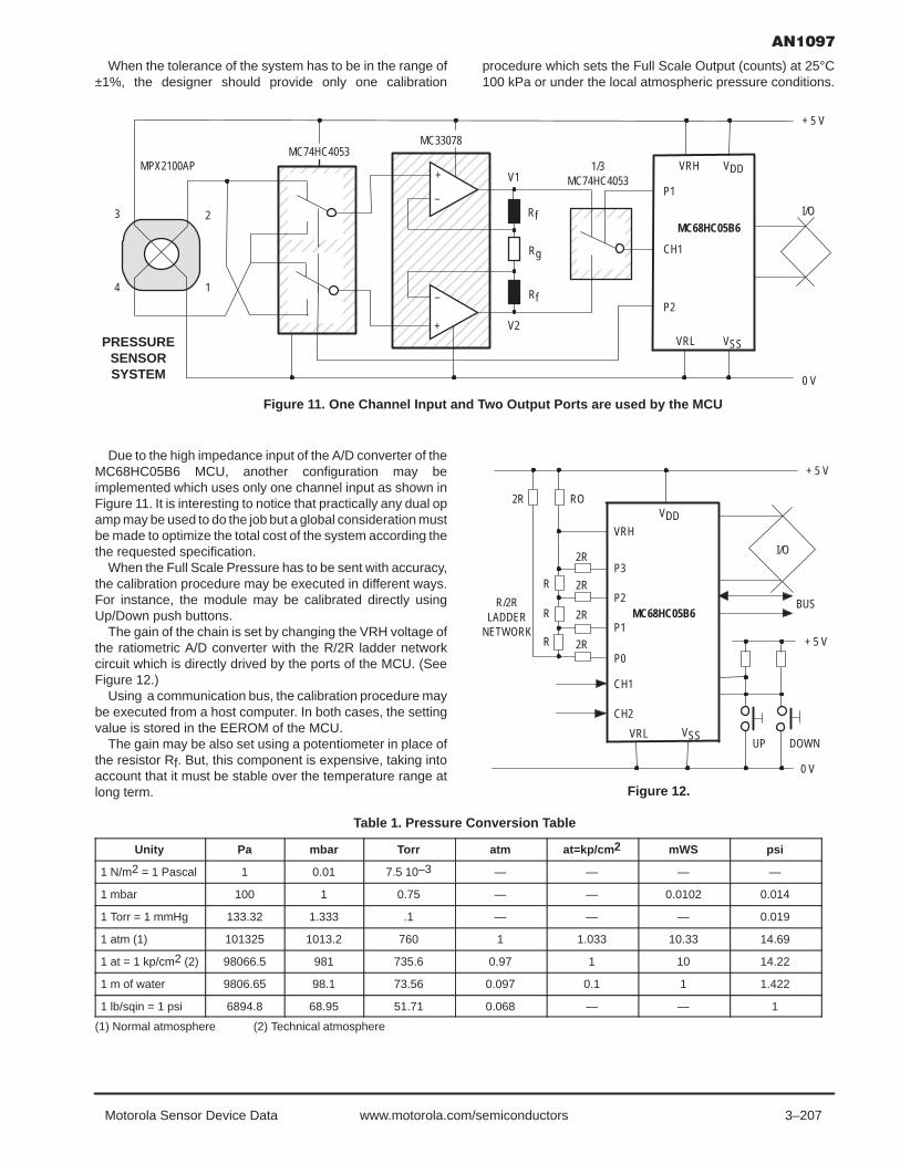
3–207Motorola Sensor Device Data www.motorola.com/semiconductors
When the tolerance of the system has to be in the range of±1%, the designer should provide only one calibration
procedure which sets the Full Scale Output (counts) at 25°C100 kPa or under the local atmospheric pressure conditions.
ÉÉÉÉÉÉÉÉÉÉÉÉ
ÉÉÉÉÉÉÉÉÉÉÉÉÉÉÉÉÉÉÉÉÉÉÉÉÉÉÉÉÉÉÉÉÉÉÉÉÉÉÉÉÉÉÉÉÉÉÉÉÉÉ
ÉÉÉÉÉÉÉÉÉÉÉÉÉÉÉÉÉÉÉÉÉÉÉÉÉÉÉÉÉÉÉÉ
1
2
4
3
PRESSURESENSORSYSTEM
MPX2100APMC74HC4053
MC33078
1/3MC74HC4053V1
V2
Rf
Rg
Rf
+ 5 V
0 V
I/OMC68HC05B6
P1
CH1
P2
VRL VSS
VRH VDD+
–
+
Figure 11. One Channel Input and Two Output Ports are used by the MCU
–
Due to the high impedance input of the A/D converter of theMC68HC05B6 MCU, another configuration may beimplemented which uses only one channel input as shown inFigure 11. It is interesting to notice that practically any dual opamp may be used to do the job but a global consideration mustbe made to optimize the total cost of the system according thethe requested specification.
When the Full Scale Pressure has to be sent with accuracy,the calibration procedure may be executed in different ways.For instance, the module may be calibrated directly usingUp/Down push buttons.
The gain of the chain is set by changing the VRH voltage ofthe ratiometric A/D converter with the R/2R ladder networkcircuit which is directly drived by the ports of the MCU. (SeeFigure 12.)
Using a communication bus, the calibration procedure maybe executed from a host computer. In both cases, the settingvalue is stored in the EEROM of the MCU.
The gain may be also set using a potentiometer in place ofthe resistor Rf. But, this component is expensive, taking intoaccount that it must be stable over the temperature range atlong term.
MC68HC05B6
VRH
P3
P2
P1
CH1
CH2
VDD
VRL VSS
2R RO
R/2RLADDER
NETWORK
2R
2R
2R
2R
R
R
R
I/O
+ 5 V
0 V
UP DOWN
+ 5 V
Figure 12.
P0
BUS
Table 1. Pressure Conversion Table
Unity Pa mbar Torr atm at=kp/cm 2 mWS psi
1 N/m2 = 1 Pascal 1 0.01 7.5 10–3 — — — —
1 mbar 100 1 0.75 — — 0.0102 0.014
1 Torr = 1 mmHg 133.32 1.333 .1 — — — 0.019
1 atm (1) 101325 1013.2 760 1 1.033 10.33 14.69
1 at = 1 kp/cm2 (2) 98066.5 981 735.6 0.97 1 10 14.22
1 m of water 9806.65 98.1 73.56 0.097 0.1 1 1.422
1 lb/sqin = 1 psi 6894.8 68.95 51.71 0.068 — — 1
(1) Normal atmosphere (2) Technical atmosphere

3–208 Motorola Sensor Device Datawww.motorola.com/semiconductors
PURPOSE
This paper describes a simple method to gain more than8–bits of resolution with an 8–bit A/D. The electronic design isrelatively simple and uses standard components.
PRINCIPLE
Consider a requirement to measure pressure up to200 kPa. Using a pressure sensor and an amplifier, thispressure can be converted to an analog voltage output. Thisanalog voltage can then be converted to a digital value andused by the microprocessor as shown in Figure 1.
If we assume for this circuit that 200 kPa results in a +4.5 Voutput, the sensitivity of our system is:/
S 4.5 V200kPa (1) 0.0225 VkPa
or S 22.5 mVkPa
If an 8–bit A/D is used with 0 and 5 Volt low and highreferences, respectively, then the resolution would be:
S 5V 28–1 5V255 (2)
0.01961 Vor Rv 19.60 mV per bit
This corresponds to a pressure resolution of:
RP 5V 19.60 mVbit) 22.5 mVkPa (3)
0.871 kPa per bit
Assume a resolution of at least 0.1 kPa/bit is needed. Thiswould require an A/D with at least 12 bits ( 212 = 4096 steps).
One can artificially increase the A/D resolution as describedbelow.
Refer to Figure 1 and assume a pressure of 124 kPa is tobe measured. With this system, the input signal to the A/Dshould read (assuming no offset voltage error):
Vm(measured) 4.5 (Papp) x (S) (4)
(124 kPa) x 22.5 mVkPa
2790 mV,
where Papp is the pressure applied to the sensor.Due to the resolution of the A/D, the microprocessor
receives the following conversion:
M (2790 mV) 19.60 mVbit (5)
142.35 142 (truncated to integer)
The calculated voltage for this stored value is:
Vc (calculated) (142 count) x 19.60mV (6)
count) 2783 mV
The microprocessor will output the stored value M to theD/A. The corresponding voltage at the analog output of theD/A, for an 8–bit D/A with same references, will be 2783 mV.
The calculated pressure corresponding to this voltagewould be:
Pc (calculated) (2783 mV) 22.5 mVkPa (7)
123.7 kPa
Thus, the error would be:
E Papp–Pc (8) 124 kPa–123.7 kPa 0.3 kPa
This is greater than the 0.1 kPa resolution requirement.
Figure 1. Block Diagram
+V
G A/D MPUOUTPUT
CIRCUITRY
Vm M Pc
SEMICONDUCTOR APPLICATION NOTE
REV 1

3–209Motorola Sensor Device Data www.motorola.com/semiconductors
A/D
MPU
+V
G
OUTPUTCIRCUITRY
G
D/A
Figure 2. Expanded Block Diagram
Vm
Vc
D
Control
C
M
M
ANALOG CIRCUITRY
–Σ
Figure 2 shows the block diagram of a system that can beused to reduce the inaccuracies caused by the limited A/Dresolution. The microprocessor would use the stored value M,as described above, to cause a D/A to output thecorresponding voltage, Vc. Vc is subtracted from themeasured voltage, Vm, using a differential amplifier, and theresulting voltage is amplified. Assuming a gain, G, of 10 for theamplifier, the output would be:
D (Vm–Vc)G (9) (2790 mV–2783 mV) 10 70 mV
The microprocessor will receive the following count from theA/D:
C 70mV19.60 mVcount (10)
3.6 3 full counts
The microprocessor then computes the actual pressurewith the following equations:
Expanded Voltage Vc CR)G) (11)
2783 3 19.60)10)
2789 mV,
NOTE: R is resolution of 8-bit d/A
Corresponding Pressure 2789 mV (12) 22.5 mVkPa 123.9 kPa
Thus the error is:
Pressure Error Actual – Measured (13) 124 kPa – 123.9 kPa 0.1 kPa
Figures 3 and 4 together provide a more detaileddescription of the analog portion of this system.
+VR3 R2 R5
R8
R9
R10
A1A2
+
R7
+V
Vm (to Second Stage)
Figure 3. First Stage – Differential Amplifier, Offset Adjust and Gain Adjust
R4
R6
R1
–
+
–
Note: R7 = R2, R1 = R6

3–210 Motorola Sensor Device Datawww.motorola.com/semiconductors
Vm(from first
stage)
R11R15
R17
A3
A4
Vm
R12
R13
R14
R16
D
Vc
Figure 4. Second Stage — Difference Amplifier and Gain
+
–
+
–
from D/A
Note: R14 = R12, R11 = R13
FIRST STAGE (Figure 3)
The first stage consists of the Motorola pressure sensor; inthis case the MPX2200 is used. This sensor typically gives afull scale span output of 40 mV at 200 kPa. The sensor output(VS) is connected to the inputs of amplifier A1 (1/4 of theMC33079, a Quad Operational Amplifier). The gain, G1, of thisamplifier is R7/R6. The sensor has a typical zero pressureoffset voltage of 1 mV. Figure 3 shows offset compensationcircuitry if it is needed. A1 output is fed to the non–invertinginput of A2 amplifier (1/4 of a MC33079) whose gain, G2, is1+R10/R9. G2 should be set to yield 4.5 volts out with full–ratedpressure.
THE SECOND STAGE (Figure 4)
The output from A2 (Vm = G1 x G2 x Vs) is connected to thenon–inverting input of amplifier A3 (1/4 of a MC33079) and tothe A/D where its corresponding (digital) value is stored by themicroprocessor. The output of A3 is the amplified differencebetween Vm, and the digitized/calculated voltage Vc.Amplifier A4 (1/4 of a MC33079) provides additional gain foran amplified difference output for the desired resolution. Thisdifference output, D, is given by:
D Vm – Vc G3
G3 R14 R131 R17R16
where G3 is the gain associated with amplifiers A3 and A4.
The theoretical resolution is limited only by the accuracy ofthe programmable power supply. The Motorolamicroprocessor used has an integrated A/D. The accuracy ofthis A/D is directly related to the reference voltage sourcestability, which can be self–calibrated by the microprocessor.Vexpanded is the system output that is the sum of the voltagedue to the count and the voltage due to the difference betweenthe count voltage and the measured voltage. This is given bythe following relation:
Vexpanded Vc DG3
therefore, PVexpanded VexpandedS.
Pexpanded is the value of pressure (in units of kPa) thatresults from this improved–resolution system. This value canbe output to a display or used for further processing in a controlsystem.
CONCLUSION
This circuit provides an easy way to have high resolutionusing inexpensive microprocessors and converters.

3–211Motorola Sensor Device Data www.motorola.com/semiconductors
!
Prepared by: Denise WilliamsDiscrete Applications Engineering
INTRODUCTION
The two wire 4–20 mA current loop is one of the most widelyutilized transmission signals for use with transducers inindustrial applications. A two wire transmitter allows signaland power to be supplied on a single wire–pair. Because theinformation is transmitted as current, the signal is relativelyimmune to voltage drops from long runs and noise frommotors, relays, switches and industrial equipment. The use ofadditional power sources is not desirable because theusefulness of this system is greatest when a signal has to betransmitted over a long distance with the sensor at a remotelocation. Therefore, the 4 mA minimum current in the loop isthe maximum usable current to power the entire controlcircuitry.
Figure 1 is a block diagram of a typical 4–20 mA currentloop system which illustrates a simple two chip solution toconverting pressure to a 4–20 mA signal. This system isdesigned to be powered with a 24 Vdc supply. Pressure isconverted to a differential voltage by the Motorola MPX5100pressure sensor. The voltage signal proportional to themonitored pressure is then converted to the 4–20 mA currentsignal with the Burr–Brown XTR101 Precision Two–WireTransmitter. The current signal can be monitored by a meterin series with the supply or by measuring the voltage dropacross RL. A key advantage to this system is that circuitperformance is not affected by a long transmission line.
ÄÄÄÄÄÄÄÄÄÄÄÄÄÄÄÄ
SENSORPRESSURE
PORT
PRESSURESOURCE
PRESSURESENSOR
TRANSMITTERCIRCUITRY
4 – 20 mA PRESSURE TRANSDUCER
TRANSMISSIONLINE RL
CURRENTMETER
24 VDC
Figure 1. System Block Diagram
SEMICONDUCTOR APPLICATION NOTE
REV 4

3–212 Motorola Sensor Device Datawww.motorola.com/semiconductors
INPUT TERMINALS
A schematic of the 4–20 mA Pressure Transducer topologyis shown in Figure 2. Connections to this topology are madeat the terminals labeled (+) and (–). Because this systemutilizes a current signal, the power supply, the load and anycurrent meter must be put in series with the (+) to (–) terminalsas indicated in the block diagram. The load for this type of
system is typically a few hundred ohms. As described above,a typical use of a 4–20 mA current transmission signal is thetransfer of information over long distances. Therefore, a longtransmission line can be connected between the (+) and (–)terminals on the evaluation board and the power supply/load.
2 14
D21N4565A
6.4V @ 0.5mA
XDCR1MPX7100
3 2
4 1
2 mA
R339
R550
45
6
3
1 7 13 9
10 11 8R1750
1/2 W
Q1MPSA06
U1XTR101
12
R6100K R4
1M
R21K
D11N4002
C10.01µF
+ 4 – 20 mA OUTPUT
– RETURN
Figure 2. Schematic Diagram
4 – 20 mA PRESSURE TRANSDUCER
PRESSURE INPUT
The device supplied on this topology is an MPX5100DP,which provides two ports. P1, the positive pressure port, is ontop of the sensor and P2, the vacuum port, is on the bottom ofthe sensor. The system can be supplied up to 15 PSI ofpositive pressure to P1 or up to 15 PSI of vacuum to P2 or adifferential pressure up to 15 PSI between P1 and P2. Any ofthese pressure applications will create the same results at thesensor output.
CIRCUIT DESCRIPTION
The XTR101 current transmitter provides two one–milliampcurrent sources for sensor excitation when its bias voltage isbetween 12 V and 40 V. The MPX5100 series sensors areconstant voltage devices, so a zener, D2, is placed in parallelwith the sensor input terminals. Because the MPX5100 seriesparts have a high impedance the zener and sensorcombination can be biased with just the two milliampsavailable from the XTR101.
The offset adjustment is composed of R4 and R6. They areused to remove the offset voltage at the differential inputs tothe XTR101. R6 is set so a zero input pressure will result inthe desired output of 4 mA.
R3 and R5 are used to provide the full scale current span of16 mA. R5 is set such that a 15 PSI input pressure results inthe desired output of 20 mA. Thus the current signal will span
16 mA from the zero pressure output of 4 mA to the full scaleoutput of 20 mA. To calculate the resistor required to set thefull scale output span, the input voltage span must be defined.The full scale output span of the sensor is 24.8 mV and is ∆VINto the XTR101. Burr–Brown specifies the following equationfor Rspan. The 40 and 16 mΩ values are parameters of theXTR101.
Rspan 40 16 mA Vin) 0.016 mhos]
64
The XTR101 requires that the differential input voltage atpins 3 and 4, V2 – V1 be less than 1V and that V2 (pin 4)always be greater than V1 (pin 3). Furthermore, thisdifferential voltage is required to have a common mode of 4–6volts above the reference (pin 7). The sensor produces thedifferential output with a common mode of approximately 3.1volts above its reference pin 1. Because the current of both 1mA sources will go through R2, a total common mode voltageof about 5.1 volts (1 kΩ x 2 mA + 3.1 volts = 5.1 volts) isprovided.
CONCLUSION
This circuit is an example of how the MPX5000 seriessensors can be utilized in an industrial application. It providesa simple design alternative where remote pressure sensing isrequired.

3–213Motorola Sensor Device Data www.motorola.com/semiconductors
Table 1. Parts List for 4–20 mA Pressure Transducer Evaluation Board
Designator Quantity Description Rating Manufacturer Part Number
114422
PC Board (see Figure 3)Input/Output Terminals1/2″ standoffs, Nylon threaded1/2″ screws, Nylon5/8″ screws, Nylon4–40 nuts, Nylon
MotorolaPHX CONT
DEVB126#1727010
C1 1Capacitor0.01 µF 50 V
D1D2
11
Diodes100 V Diode6.4 V Zener
1 A 1N40021N4565A
Q1 1TransistorNPN Bipolar Motorola MPSA06
R1 R2 R3 R4
1111
Resistors, Fixed750 Ω1 kΩ39 Ω1 MΩ
1/2 W
R5 R6
11
Resistors, Variable50 Ω, one turn100 KΩ, one turn
Bourns Bourns
#3386P–1–500 #3386P–1–104
U1 1Integrated CircuitTwo wire current transmitter Burr–Brown XTR101
XDCR1 1SensorHigh Impedance 15 PSI Motorola MPX5100DP
NOTE: All resistors are 1/4 W with a tolerance of 5% unless otherwise noted. All capacitors are 100 volt, ceramic capacitors with a toleranceof 10% unless otherwise noted.

3–214 Motorola Sensor Device Datawww.motorola.com/semiconductors
! !
Prepared by: Warren SchultzDiscrete Applications Engineering
INTRODUCTION
Integrated semiconductor pressure sensors such as theMPX5100 greatly simplify electronic measurement ofpressure. These devices translate pressure into a 0.5 to 4.5volt output range that is designed to be directly compatiblewith microcomputer A/D inputs. The 0.5 to 4.5 volt range also
facilitates interface with ICs such as the LM3914, making BarGraph Pressure Gauges relatively simple. A description of aBar Graph Pressure Sensor Evaluation Board and its designconsiderations are presented here.
Figure 1. DEVB129 MPX5100 Bar Graph Pressure Gauge(Board No Longer Available)
SEMICONDUCTOR APPLICATION NOTE
REV 1

3–215Motorola Sensor Device Data www.motorola.com/semiconductors
EVALUATION BOARD DESCRIPTION
A summary of the information required to use evaluationboard number DEVB129 is presented as follows. A discussionof the design appears under the heading DesignConsiderations.
FUNCTIONThe evaluation board shown in Figure 1 is designed to
provide a 100 kPa full scale pressure measurement. It has twoinput ports. P1, the pressure port is on the top side of theMPX5100 sensor, and P2, a vacuum port, is on the bottomside. These ports can be supplied up to 100 kPa (15 psi)* ofpressure on P1 or up to 100 kPa of vacuum on P2, or adifferential pressure up to 100 kPa between P1 and P2. Anyof these sources will produce the same output.
The primary output is a 10 segment LED bar graph, whichis labeled in increments of 10 kPa. If full scale pressure isadjusted for a value other than 100 kPa the bar graph may beread as a percent of full scale. An analog output is alsoprovided. It nominally supplies 0.5 volts at zero pressure and4.5 volts at 100 kPa. Zero and full scale adjustments are madewith potentiometers so labeled at the bottom of the board.Both adjustments are independent of each other.
ELECTRICAL CHARACTERISTICSThe following electrical characteristics are included to
describe evaluation board operation. They are notspecifications in the usual sense and are intended only as aguide to operation.
Characteristic Symbol Min Typ Max Units
Power Supply Voltage B+ 6.8 — 13.2 Volts
Full Scale Pressure PFS — — 100 kPa
Overpressure PMAX — — 700 kPa
Analog Full Scale VFS — 4.5 — Volts
Analog Zero PressureOffset
VOFF — 0.5 — Volts
Analog Sensitivity SAOUT — 40 — mV/kPa
Quiescent Current ICC — 20 — mA
Full Scale Current IFS — 140 — mA
CONTENTBoard contents are described in the following parts list,
schematic, and silk screen plot. A pin by pin circuit descriptionfollows in the next section.
PIN–BY–PIN DESCRIPTION
B+:Input power is supplied at the B+ terminal. Minimum input
voltage is 6.8 volts and maximum is 13.2 volts. The upper limitis based upon power dissipation in the LM3914 assuming all10 LED’s are lit and ambient temperature is 25°C. The boardwill survive input transients up to 25 volts provided that powerdissipation in the LM3914 does not exceed 1.3 watts.
OUT:An analog output is supplied at the OUT terminal. The signal
it provides is nominally 0.5 volts at zero pressure and 4.5 voltsat 100 kPa. This output is capable of sourcing 100 µA at fullscale output.
GND:There are two ground connections. The ground terminal on
the left side of the board is intended for use as the powersupply return. On the right side of the board, one of the testpoint terminals is also connected to ground. It provides aconvenient place to connect instrumentation grounds.
TP1:Test point 1 is connected to the zero pressure reference
voltage and can be used for zero pressure calibration. Tocalibrate for zero pressure, this voltage is adjusted with R6 tomatch the zero pressure voltage that is measured at theanalog output (OUT) terminal.
TP2:Test point 2 performs a similar function at full scale. It is
connected to the LM3914’s reference voltage which sets thetrip point for the uppermost LED segment. This voltage isadjusted via R5 to set full scale pressure.
P1, P2:Pressure and Vacuum ports P1 & P2 protrude from the
MPX5100 sensor on the right side of the board. Pressure portP1 is on the top and vacuum port P2 is on the bottom. Neitheris labeled. Either one or a differential pressure applied to bothcan be used to obtain full scale readings up to 100 kPa (15 psi).Maximum safe pressure is 700 kPa.
* 100 kPa = 14.7 psi, 15 psi is used throughout the text for convenience

3–216 Motorola Sensor Device Datawww.motorola.com/semiconductors
DESIGN CONSIDERATIONS
In this type of an application the design challenge is how tointerface a sensor with the bar graph output. MPX5100Sensors and LM3914 Bar Graph Display drivers fit together socleanly that having selected these two devices the rest of thedesign is quite straight forward.
A block diagram that appears in Figure 4 shows theLM3914’s internal architecture. Since the lower resistor in theinput comparator chain is pinned out at RLO, it is a simplematter to tie this pin to a voltage that is approximately equalto the MPX5100’s zero pressure output voltage. In Figure 2,this is accomplished by dividing down the 5 volt regulator’soutput voltage through R1, R4, and adjustment pot R6. Thevoltage generated at the wiper of R6 is then fed into RLO whichmatches the sensor’s zero pressure voltage and zeros the bargraph.
The full scale measurement is set by adjusting the uppercomparator’s reference voltage to match the sensor’s outputat full pressure. An internal regulator on the LM3914 sets thisvoltage with the aid of resistors R2, R3, and adjustment pot R5that are shown in Figure 2.
The MPX5100 requires 5 volt regulated power thatis supplied by an MC78L05. The LED’s are powereddirectly from LM3914 outputs, which are set up as currentsources. Output current to each LED is approximately10 times the reference current that flows from pin 7 throughR2, R5, and R3 to ground. In this design it is nominally(4.5 V/4.9K)10 = 9.2 mA.
Over a zero to 85°C temperature range accuracy for boththe sensor and driver IC are ±2.5%, totaling ±5%. Given a 10segment display total accuracy is approximately ±(10 kPa+5%).
CONCLUSION
Perhaps the most noteworthy aspect to the bar graphpressure gauge described here is how easy it is to design. Theinterface between an MPX5100 sensor, LM3914 displaydriver, and bar graph output is direct and straight forward. The
result is a simple circuit that is capable of measuring pressure,vacuum, or differential pressure; and will also send an analogsignal to other control circuitry.
Figure 2. MPX5100 Pressure Gauge
S1
ON/OFF
123456789
181716151413121110
LEDLEDGNDB+RLOSIGRHIREFADJMOD
U1U1
LM3914
TP2 (FULL SCALE CALIBRATION)
TP1 (ZERO CALIBRATION)
GNDFULL SCALE CALIBRATION
D1 D2 D3 D4 D5 D6 D7 D8 D9 D10
R21.2 k
R51 k
R32.7 k
R1100
R6100
U2MPX5100
1
2
3
1
2
3I
GO
GND
ANALOG OUT
+12 V
C10.1 µF
C21 µF
U3
MC78L05ACP
ZEROCAL.
R4
1.3K
LEDLEDLEDLEDLEDLEDLED
LED
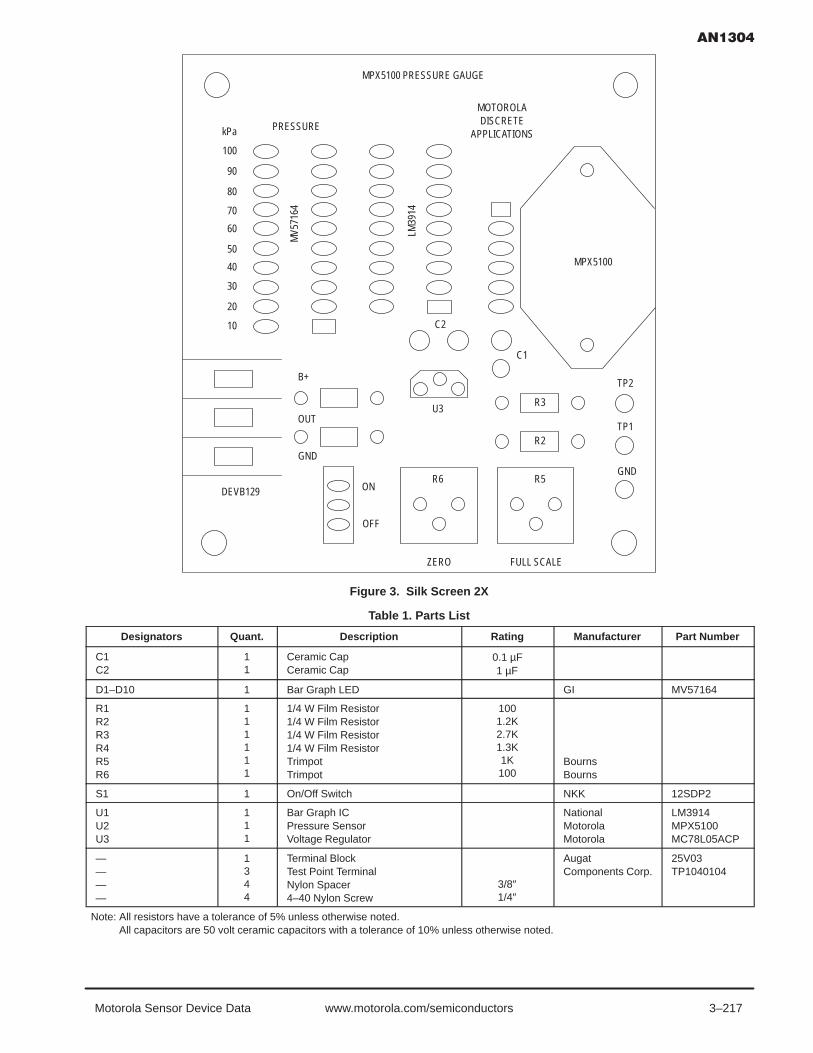
3–217Motorola Sensor Device Data www.motorola.com/semiconductors
Figure 3. Silk Screen 2X
U3R3
R2
R5R6
FULL SCALE
DEVB129 ON
OFF
B+
OUT
GND
TP1
TP2
GND
C1
C2
MPX5100
kPa
100
90
80
70
60
50
40
30
20
10
PRESSURE
MV5
7164
LM39
14
MOTOROLADISCRETE
APPLICATIONS
MPX5100 PRESSURE GAUGE
ZERO
Table 1. Parts List
Designators Quant. Description Rating Manufacturer Part Number
C1C2
11
Ceramic CapCeramic Cap
0.1 µF1 µF
D1–D10 1 Bar Graph LED GI MV57164
R1R2R3R4R5R6
111111
1/4 W Film Resistor1/4 W Film Resistor1/4 W Film Resistor1/4 W Film ResistorTrimpotTrimpot
1001.2K2.7K1.3K1K100
BournsBourns
S1 1 On/Off Switch NKK 12SDP2
U1U2U3
111
Bar Graph ICPressure SensorVoltage Regulator
NationalMotorolaMotorola
LM3914MPX5100MC78L05ACP
————
1344
Terminal BlockTest Point TerminalNylon Spacer4–40 Nylon Screw
3/8″1/4″
AugatComponents Corp.
25V03TP1040104
Note: All resistors have a tolerance of 5% unless otherwise noted.Note: All capacitors are 50 volt ceramic capacitors with a tolerance of 10% unless otherwise noted.

3–218 Motorola Sensor Device Datawww.motorola.com/semiconductors
Figure 4. LM3914 Block Diagram
REFERENCEVOLTAGESOURCE
1.25 V
MODESELECT
AMPLIFIER–
+
BUFFER
REFOUT
THIS LOADDETERMINES
LEDBRIGHTNESS
CONTROLSTYPE OFDISPLAY, BAROR SINGLELED
COMPARATOR1 of 10
LM3914
10
11
12
13
14
15
16
17
18
1
1 k
1 k
1 k
1 k
1 k
1 k
1 k
1 k
1 k
1 k
LEDV+
RHI 6
7
8
3
4
5
RLO
REFADJ
V+
SIGIN
V–
9
2
FROMPIN 11V+
20 k
+
–
+–
+–
+–
+–
+–
+–
+–
+–
+–
+–

3–219Motorola Sensor Device Data www.motorola.com/semiconductors
"! $ ! #
Prepared by: Bill LucasDiscrete Applications Engineering
INTRODUCTION
Interfacing pressure sensors to analog–to–digitalconverters or microprocessors with on–chip A/D convertershas been a challenge that most engineers do not enjoyaccepting. Recent design advances in pressure sensingtechnology have allowed the engineer to directly interface apressure sensor to an A/D converter with no additional active
components. This has been made possible by integrating atemperature compensated pressure sensor element andactive linear circuitry on the same die. A description of anevaluation board that shows the ease of interfacing a signalconditioned pressure sensor to an A/D converter is presentedhere.
Figure 1. DEVB–114 MPX5100 Evaluation Module(Board No Longer Available)
SEMICONDUCTOR APPLICATION NOTE
REV 1

3–220 Motorola Sensor Device Datawww.motorola.com/semiconductors
PURPOSE
This evaluation system, shown in Figure 1, demonstratesthe ease of operation and interfacing of the MotorolaMPX5100 series pressure sensors with on–chip temperaturecompensation, calibration and amplification. The board maybe used to evaluate the sensor’s suitability for a specificapplication.
DESCRIPTION
The DEVB–114 evaluation board is constructed on a smallprinted circuit board. It is powered from a single +5 Vdcregulated power supply. The system will display the pressureapplied to the MPX5100 sensor in pounds per square inch.The range is 0 PSI through 15 PSI, resolved to 0.1 PSI. Nopotentiometers are used in the system to adjust the span and
offset. The sensor’s zero offset voltage with no pressureapplied to the sensor is empirically computed each time poweris applied to the system and stored in RAM. The sensitivity ofthe MPX5100 is repeatable from unit to unit. There is a facilityfor a small “rubbering” of the slope constant built into theprogram. It is accomplished with jumpers J1 and J2, and isexplained in the Operation section. The board contents arefurther described in the schematic, silk screen plot, and partslist that appear in Figures 2, 3 and Table 1.
BASIC CIRCUIT
The evaluation board consists of three basic subsystems:an MPX5100GP pressure sensor, a four digit liquid crystaldisplay (only three digits and a decimal are used) and aprogrammed microprocessor with the necessary externalcircuitry to support the operation of the microprocessor.
3029 2827262524313837 363534333248 454442 43 464749
44VSS ∼.302 V
∼4.85 V
15 OHM
453 OHM
22 pF
100 µF
52
50
TD0
RDI
5
PORTAPORTB
3456712034567127 6 5 4 32 10
PORTC
GND
VPP6
151%
1%
1%
30.1 OHM
XDCR1
RESET
IN
U1
U234064P–
5
.1+
10K
10K 4.7K
22 pF10MEG
4 MHzY1
C4C3
C2C1
R7
R6
R5
R4
R3
R2
R1
J3
MC68HC705B5FN
+5
OUT
VCC
MPX5100
TCAP2TCAP1
D/APD5 PD0PD1
PD2PD3PD4
VDD
+5
PD7PD6
1716
OSC2OSC1
+5
8
7
VRH
VRL
+5
GND
+5
18
RESETIRQ
194 3
J2J1
+5
1–4, 3339, 38, 40
28
BP
IEE PART NUMBER LCD5657 OR EQUALLIQUID CRYSTAL DISPLAY
2637 36 3534 3231 3029 27 2524 2322 212019141211 17 181615131098765
14131211109 21 22 23
LCD
Figure 2. DEVB–114 System Schematic
___ ______

3–221Motorola Sensor Device Data www.motorola.com/semiconductors
Table 1. DEVB–114 Parts List
Designators Quant. Description Rating Manufacturer Part Number
C1 1 100 µF Electrolytic Capacitor 25 Vdc Sprague 513D107M025BB4
C2 1 0.1 µF Ceramic Capacitor 50 Vdc Sprague 1C105Z5U104M050B
C3, C4 2 22 pF Ceramic Capacitor 100 Vdc Mepco/Centralab CN15A220K
J1, J2 1 Dual Row Straight .025 PinsArranged On .1″ Grid Molex 10–89–1043
LCD 1 Liquid Crystal Display AMPEREX LTD226R–12
R1 1 4.7 k Ohm Resistor
R2 1 10 Meg Ohm Resistor
R3, R4 2 10 k Ohm Resistor
R5 1 15 Ohm 1% 1/4 W Resistor
R6 1 453 Ohm 1% 1/4 W Resistor
R7 1 30.1 Ohm 1% 1/4 W Resistor
XDCR1 1 Pressure Sensor Motorola MPX5100GP
U1 1 Microprocessor Motorola MC68HC705B5FN orMotorola XC68HC705B5FN
U2 1 Under Voltage Detector Motorola MC34064P–5
Y1 1 Crystal (Low Profile) 4.0 MHz ECS ECS–40–S–4
No Designator 1 52 Pin PLCC Socket AMP 821–575–1
No Designator 2 Jumpers For J1 and J2 Molex 15–29–1025
No Designator 1 Bare Printed Circuit Board
Note: All resistors are 1/4 W resistors with a tolerance of 5% unless otherwise noted.Note: All capacitors are 100 volt, ceramic capacitors with a tolerance of 10% unless otherwise noted.
Figure 3. Silk Screen
DEVB–114REV. 0
GND
+5
J3
R3R4R5R6R7
J1J2 R1
U2
TP1VCC
1
R2
Y1C4C3C2
C1
XDRC1
LCD1
U1
XDRC OUT
GND TP3
TP2

3–222 Motorola Sensor Device Datawww.motorola.com/semiconductors
Theory of OperationReferring to the schematic, Figure 2, the MPX5100
pressure sensor is connected to PORT D bit 5 of themicroprocessor. This port is an input to the on–chip 8 bitanalog to digital converter. The pressure sensor provides asignal output to the microprocessor of approximately 0.5 Vdcat 0 psi to 4.5 Vdc at 15 psi of applied pressure as shown inFigure 4. The input range of the A to D converter is set atapproximately 0.3 Vdc to 4.85 Vdc. This compresses therange of the A to D converter around the output range of thesensor to maximize the A to D converter resolution; 0 to 255counts is the range of the A to D converter. VRH and VRL arethe reference voltage inputs to the A to D converter. Theresolution is defined by the following:
Analog–to–digital converter count =
[(Vxdcr – VRL)/(VRH – VRL)] • 255
The count at 0 psi = [(.5 – .302)/(4.85 – .302)] • 255 ≈ 11The count at 15 psi = [(4.5 – .302)/(4.85 – .302)] • 255 ≈ 235Therefore the resolution = count @ 15 psi – count @ 0 psi orthe resolution is (235 – 11) = 224 counts. This translates to asystem that will resolve to 0.1 psi.
MIN
TYP
MAX
OU
TPU
T (V
dc)
kPaPSI
4.5
0.5
00 25 50 75 100
3.62 7.25 10.87 14.5
TYPSPAN
TYP OFFSET
VS = 5.0 VdcTA = 25°CMPX5100
Figure 4. MPX5100 Output versus Pressure Input
The voltage divider consisting of R5 through R7 isconnected to the +5 volts powering the system. The output ofthe pressure sensor is ratiometric to the voltage applied to it.The pressure sensor and the voltage divider are connected toa common supply; this yields a system that is ratiometric. Bynature of this ratiometric system, variations in the voltage ofthe power supplied to the system will have no effect on thesystem accuracy.
The liquid crystal display is directly driven from I/O ports A,B, and C on the microprocessor. The operation of a liquidcrystal display requires that the data and backplane pins mustbe driven by an alternating signal. This function is provided bya software routine that toggles the data and backplane atapproximately a 30 Hz rate.
The microprocessor section of the system requires certainsupport hardware to allow it to function. The MC34064P–5(U2) provides an under voltage sense function which is usedto reset the microprocessor at system power–up. The 4 MHzcrystal (Y1) provides the external portion of the oscillatorfunction for clocking the microprocessor and provides a stablebase for time based functions. Jumpers J1 and J2 areexamined by the software and are used to “rubber” the slopeconstant.
OPERATION
The system must be connected to a 5 Vdc regulated powersupply. Note the polarity marked on the power terminal J3.Jumpers J1 and J2 must either both be installed or both beremoved for the normal slope constant to be used. Thepressure port on the MPX5100 sensor must be left open toatmosphere anytime the board is powered–up. As previouslystated, the sensor’s voltage offset with zero pressure appliedis computed at power–up.
You will need to apply power to the system. The LCD willdisplay CAL for approximately 5 seconds. After that time, theLCD will then start displaying pressure.
To improve upon the accuracy of the system, you canchange the constant used by the program that constitutes thespan of the sensor. You will need an accurate test gauge tomeasure the pressure applied to the sensor. Anytime after thedisplay has completed the zero calculation (after CAL is nolonger displayed), apply 15.0 PSI to the sensor. Make surethat jumpers J1 and J2 are either both installed or bothremoved. Referring to Table 2, you can increase the displayedvalue by installing J1 and removing J2. Conversely, you candecrease the displayed value by installing J2 and removingJ1.
J1 J2 Action
INOUTOUT
IN
INOUT
IN
OUT
USE NORMAL SPAN CONSTANTUSE NORMAL SPAN CONSTANTDECREASE SPAN CONSTANT
APPROXIMATELY 1.5%INCREASE SPAN CONSTANT
APPROXIMATELY 1.5%
Table 2.
SOFTWARE
The source code, compiler listing, and S–record output forthe software used in this system are available on the MotorolaFreeware Bulletin Board Service in the MCU directory underthe filename DEVB–114.ARC. To access the bulletin boardyou must have a telephone line, a 300, 1200 or 2400 baudmodem and a terminal or personal computer. The modemmust be compatible with the Bell 212A standard. Call1–512–891–3733 to access the Bulletin Board Service.
The software for the system consists of several modules.Their functions provide the capability for system calibration aswell as displaying the pressure input to the MPX5100transducer.
Figure 5 is a flowchart for the program that controls thesystem.

3–223Motorola Sensor Device Data www.motorola.com/semiconductors
Figure 5. DEVB–114 Software Flowchart
YES
START
NO
INITIALIZE DISPLAY I/O PORTSINITIALIZE TIMER REGISTERS
ALLOW INTERRUPTSPERFORM AUTO ZERO
TIMERINTERRUPT
J1 OUT?
ACCUMULATE 100 A/D CONVERSIONSCOMPUTE INPUT PRESSURE
CONVERT TO DECIMALPLACE IN RESULT OUTPUT BUFFER
SERVICE TIMER REGISTERSSETUP COUNTER FOR NEXT INTERRUPT
SERVICE LIQUID CRYSTAL DISPLAYRETURN FROM INTERRUPT
SLOPE = 64
SLOPE = 63
J2 OUT?
NO
SLOPE = 65YES
The compiler used in this project was provided by BYTECRAFT LTD. (519) 888–6911. A compiler listing of theprogram is included at the end of this document. The followingis a brief explanation of the routines:
delay() Used to provide approximately a 20 ms loop.
read_a2d() Performs one hundred reads on the analog todigital converter on multiplexer channel 5 and returns theaccumulation.
fixcompare() Services the internal timer for 30 ms timercompare interrupts.
TIMERCMP() Alternates the data and backplane for theliquid crystal display.
initio() Sets up the microcomputer’s I/O ports, timer, allowsprocessor interrupts, and calls adzero().
adzero() This routine is necessary at power–up timebecause it delays the power supply and allows the
transducer to stabilize. It then calls ‘read_atod()’ and savesthe returned value as the sensors output voltage with zeropressure applied.
cvt_bin_dec(unsigned long arg) This routine converts theunsigned binary argument passed in ‘arg’ to a five digitdecimal number in an array called ‘digit’. It then uses thedecimal results for each digit as an index into a table thatconverts the decimal number into a segment pattern forthe display. It is then output to the display.
display_psi() This routine is called from ‘main()’. The ana-log to digital converter routine is called, the pressure iscalculated, and the pressure applied to the sensor is dis-played. The loop then repeats.
main() This is the main routine called from reset. It calls‘initio()’ to set up the system’s I/O. ‘display_psi()’ is calledto compute and display the pressure applied to the sensor.

3–224 Motorola Sensor Device Datawww.motorola.com/semiconductors
SOFTWARE SOURCE/ASSEMBLY PROGRAM CODE
#pragma option v ; /* rev 1.1 code rewritten to use the MC68HC705B5 instead of the MC68HC805B6. WLL 6/17/91 THE FOLLOWING ’C’ SOURCE CODE IS WRITTEN FOR THE DEVB–114 DEMONSTRATION BOARD. IT WAS COMPILED WITH A COMPILER COURTESY OF:
BYTE CRAFT LTD. 421 KING ST. WATERLOO, ONTARIO CANADA N2J 4E4 (519)888–6911 SOME SOURCE CODE CHANGES MAY BE NECESSARY FOR COMPILATION WITH OTHER COMPILERS. BILL LUCAS 8/5/90 MOTOROLA, SPS */
0800 1700 #pragma memory ROMPROG [5888] @ 0x0800 ;0050 0096 #pragma memory RAMPAGE0 [150] @ 0x0050 ;
/* Vector assignments */1FFE #pragma vector __RESET @ 0x1ffe ;1FFC #pragma vector __SWI @ 0x1ffc ;1FFA #pragma vector IRQ @ 0x1ffa ;1FF8 #pragma vector TIMERCAP @ 0x1ff8 ;1FF6 #pragma vector TIMERCMP @ 0x1ff6 ;1FF4 #pragma vector TIMEROV @ 0x1ff4 ;1FF2 #pragma vector SCI @ 0x1ff2 ;
#pragma has STOP ; #pragma has WAIT ; #pragma has MUL ;
/* Register assignments for the 68HC705B5 microcontroller */0000 #pragma portrw porta @ 0x00; /* */0001 #pragma portrw portb @ 0x01; /* */0002 #pragma portrw portc @ 0x02; /* */0003 #pragma portrw portd @ 0x03; /* in ,– ,SS ,SCK ,MOSI,MISO,TxD,RxD */0004 #pragma portrw ddra @ 0x04; /* Data direction, Port A */0005 #pragma portrw ddrb @ 0x05; /* Data direction, Port B */0006 #pragma portrw ddrc @ 0x06; /* Data direction, Port C (all output) */0007 #pragma portrw eeclk @ 0x07; /* eeprom/eclk cntl */0008 #pragma portrw addata @ 0x08; /* a/d data register */0009 #pragma portrw adstat @ 0x09; /* a/d stat/control */000A #pragma portrw plma @ 0x0a; /* pulse length modulation a */000B #pragma portrw plmb @ 0x0b; /* pulse length modulation b */000C #pragma portrw misc @ 0x0c; /* miscellaneous register */000D #pragma portrw scibaud @ 0x0d; /* sci baud rate register */000E #pragma portrw scicntl1 @ 0x0e; /* sci control 1 */000F #pragma portrw scicntl2 @ 0x0f; /* sci control 2 */0010 #pragma portrw scistat @ 0x10; /* sci status reg */

3–225Motorola Sensor Device Data www.motorola.com/semiconductors
0011 #pragma portrw scidata @ 0x11; /* SCI Data */0012 #pragma portrw tcr @ 0x12; /* ICIE,OCIE,TOIE,0;0,0,IEGE,OLVL */0013 #pragma portrw tsr @ 0x13; /* ICF,OCF,TOF,0; 0,0,0,0 */0014 #pragma portrw icaphi1 @ 0x14; /* Input Capture Reg (Hi–0x14, Lo–0x15) */0015 #pragma portrw icaplo1 @ 0x15; /* Input Capture Reg (Hi–0x14, Lo–0x15) */0016 #pragma portrw ocmphi1 @ 0x16; /* Output Compare Reg (Hi–0x16, Lo–0x17)*/0017 #pragma portrw ocmplo1 @ 0x17; /* Output Compare Reg (Hi–0x16, Lo–0x17)*/0018 #pragma portrw tcnthi @ 0x18; /* Timer Count Reg (Hi–0x18, Lo–0x19) */0019 #pragma portrw tcntlo @ 0x19; /* Timer Count Reg (Hi–0x18, Lo–0x19) */001A #pragma portrw acnthi @ 0x1A; /* Alternate Count Reg (Hi–$1A, Lo–$1B) */001B #pragma portrw acntlo @ 0x1B; /* Alternate Count Reg (Hi–$1A, Lo–$1B) */001C #pragma portrw icaphi2 @ 0x1c; /* Input Capture Reg (Hi–0x1c, Lo–0x1d) */001D #pragma portrw icaplo2 @ 0x1d; /* Input Capture Reg (Hi–0x1c, Lo–0x1d) */001E #pragma portrw ocmphi2 @ 0x1e; /* Output Compare Reg (Hi–0x1e, Lo–0x1f)*/001F #pragma portrw ocmplo2 @ 0x1f; /* Output Compare Reg (Hi–0x1e, Lo–0x1f)*/
/* put constants and variables here...they must be global */
/***********************************************************************/1EFE 74 #pragma mor @ 0x1EFE = 0x74; /* this disables the watchdog counter and does not add pull–down resistors on ports B and C */
0800 FC 30 DA 7A 36 6E E6 38 FE const char lcdtab[]=0xfc,0x30,0xda,0x7a,0x36,0x6e,0xe6,0x38,0xfe,0x3e ;0809 3E /* lcd pattern table 0 1 2 3 4 5 6 7 8 9 */080A 27 10 03 E8 00 64 00 0A const long dectable[] = 10000, 1000, 100, 10 ;
0050 0005 unsigned int digit[5]; /* buffer to hold results from cvt_bin_dec functio */
0000 registera ac; /* processor’s A register */
0055 long atodtemp; /* temp to accumulate 100 a/d readings for smoothing */
0059 long slope; /* multiplier for adc to engineering units conversion */
005B int adcnt; /* a/d converter loop counter */
005C long xdcr_offset; /* initial xdcr offset */
005E 0060 unsigned long i,j; /* counter for loops */
0062 int k; /* misc variable */
struct bothbytes int hi; int lo; ;
union isboth long l; struct bothbytes b; ;
0063 0002 union isboth q; /* used for timer set–up */
3–226 Motorola Sensor Device Datawww.motorola.com/semiconductors
/**************************************************************************/ /* code starts here */ /**************************************************************************/ /* these interrupts are not used...give them a graceful return if for some reason one occurs */
1FFC 08 12 __SWI()0812 80 RTI1FFA 08 13 IRQ()0813 80 RTI1FF8 08 14 TIMERCAP()0814 80 RTI1FF4 08 15 TIMEROV()0815 80 RTI1FF2 08 16 SCI()0816 80 RTI
/**************************************************************************/
void delay(void) /* just hang around for a while */ 0817 4F CLRA for (i=0; i<20000; ++i);0818 3F 57 CLR $57 081A B7 58 STA $58 081C B6 57 LDA $57 081E B7 5E STA $5E 0820 B6 58 LDA $58 0822 B7 5F STA $5F 0824 B6 5F LDA $5F 0826 A0 20 SUB #$20 0828 B6 5E LDA $5E 082A A2 4E SBC #$4E 082C 24 08 BCC $0836 082E 3C 5F INC $5F 0830 26 02 BNE $0834 0832 3C 5E INC $5E 0834 20 EE BRA $0824 0836 81 RTS /**************************************************************************/
read_a2d(void) /* read the a/d converter on channel 5 and accumulate the result in atodtemp */
0837 3F 56 CLR $56 atodtemp=0; /* zero for accumulation */0839 3F 55 CLR $55083B 4F CLRA for ( adcnt = 0 ; adcnt<100; ++adcnt) /* do 100 a/d conversions */083C B7 5B STA $5B 083E B6 5B LDA $5B 0840 A8 80 EOR #$80 0842 A1 E4 CMP #$E4 0844 24 21 BCC $0867

3–227Motorola Sensor Device Data www.motorola.com/semiconductors
0846 A6 25 LDA #$25 adstat = 0x25; /* convert on channel 5 */0848 B7 09 STA $09 084A 0F 09 FD BRCLR 7,$09,$084A while (!(adstat & 0x80)); /* wait for a/d to complete */084D B6 08 LDA $08 atodtemp = addata + atodtemp;084F 3F 57 CLR $57 0851 B7 58 STA $58 0853 BB 56 ADD $56 0855 B7 58 STA $58 0857 B6 57 LDA $57 0859 B9 55 ADC $55 085B B7 57 STA $57 085D B7 55 STA $55 085F B6 58 LDA $58 0861 B7 56 STA $56 0863 3C 5B INC $5B 0865 20 D7 BRA $083E 0867 B6 56 LDA $56 atodtemp = atodtemp/100;0869 B7 58 STA $58 086B B6 55 LDA $55 086D B7 57 STA $57 086F 3F 66 CLR $66 0871 A6 64 LDA #$64 0873 B7 67 STA $67 0875 CD 0A 5E JSR $0A5E 0878 CD 0A 8F JSR $0A8F 087B BF 55 STX $55 087D B7 56 STA $56 087F 81 RTS return atodtemp;
/**************************************************************************/
void fixcompare (void) /* sets–up the timer compare for the next interrup */ 0880 B6 18 LDA $18 q.b.hi =tcnthi;0882 B7 63 STA $63 0884 B6 19 LDA $19 q.b.lo = tcntlo;0886 B7 64 STA $64 0888 AB 4C ADD #$4C q.l +=7500; /* ((4mhz xtal/2)/4) = counter period = 2us.*7500 = 15ms.*/088A B7 64 STA $64 088C B6 63 LDA $63 088E A9 1D ADC #$1D 0890 B7 63 STA $63 0892 B7 16 STA $16 ocmphi1 = q.b.hi;0894 B6 13 LDA $13 ac=tsr;0896 B6 64 LDA $64 ocmplo1 = q.b.lo;0898 B7 17 STA $17 089A 81 RTS
/*************************************************************************/ void TIMERCMP (void) /* timer service module */1FF6 08 9B

3–228 Motorola Sensor Device Datawww.motorola.com/semiconductors
089B 33 02 COM $02 portc =~ portc; /* service the lcd */089D 33 01 COM $01 portb =~ portb;089F 33 00 COM $00 porta =~ porta;08A1 AD DD BSR $0880 fixcompare();08A3 80 RTI
/************************************************************************/
void adzero(void) /* called by initio() to save initial xdcr’s zero pressure offset voltage output */
08A4 4F CLRA for ( j=0; j<20; ++j) /* give the sensor time to ”warm–up” and the08A5 3F 57 CLR $57 08A7 B7 58 STA $58 08A9 B6 57 LDA $57 08AB B7 60 STA $60 08AD B6 58 LDA $58 08AF B7 61 STA $61 08B1 B6 61 LDA $61 08B3 A0 14 SUB #$14 08B5 B6 60 LDA $60 08B7 A2 00 SBC #$00 08B9 24 0B BCC $08C6 power supply time to settle down */ 08BB CD 08 17 JSR $0817 delay(); 08BE 3C 61 INC $61 08C0 26 02 BNE $08C4 08C2 3C 60 INC $60 08C4 20 EB BRA $08B1 08C6 CD 08 37 JSR $0837 xdcr_offset = read_a2d();08C9 3F 5C CLR $5C 08CB B7 5D STA $5D 08CD 81 RTS
/**************************************************************************/
void initio (void) /* setup the I/O */ 08CE A6 20 LDA #$20 adstat = 0x20; /* power–up the A/D */08D0 B7 09 STA $09 08D2 3F 02 CLR $02 porta = portb = portc = 0;08D4 3F 01 CLR $01 08D6 3F 00 CLR $00 08D8 A6 FF LDA #$FF ddra = ddrb = ddrc = 0xff;08DA B7 06 STA $06 08DC B7 05 STA $05 08DE B7 04 STA $04 08E0 B6 13 LDA $13 ac=tsr; /* dummy read */08E2 3F 1E CLR $1E ocmphi1 = ocmphi2 = 0;08E4 3F 16 CLR $16 08E6 B6 1F LDA $1F ac = ocmplo2; /* clear out output compare 2 if it happens to be set */08E8 AD 96 BSR $0880 fixcompare(); /* set–up for the first timer interrupt */
3–229Motorola Sensor Device Data www.motorola.com/semiconductors
08EA A6 40 LDA #$40 tcr = 0x40;08EC B7 12 STA $12 08EE 9A CLI CLI; /* let the interrupts begin ! */ /* write CAL to the display */08EF A6 CC LDA #$CC portc = 0xcc; /* C */08F1 B7 02 STA $02 08F3 A6 BE LDA #$BE portb = 0xbe; /* A */08F5 B7 01 STA $01 08F7 A6 C4 LDA #$C4 porta = 0xc4; /* L */08F9 B7 00 STA $00 08FB AD A7 BSR $08A4 adzero();08FD 81 RTS
/**************************************************************************/ void cvt_bin_dec(unsigned long arg)
/* First converts the argument to a five digit decimal value. The msd is in the lowest address. Then leading zero suppresses the value and writes it to the display ports. The argument value range is 0..65535 decimal. */
0069 08FE BF 69 STX $69 0900 B7 6A STA $6A 006B char i;006C unsigned long l;0902 4F CLRA for ( i=0; i < 5; ++i )0903 B7 6B STA $6B 0905 B6 6B LDA $6B 0907 A1 05 CMP #$05 0909 24 07 BCC $0912 090B 97 TAX digit[i] = 0x0; /* put blanks in all digit positions */090C 6F 50 CLR $50,X 090E 3C 6B INC $6B 0910 20 F3 BRA $0905 0912 4F CLRA for ( i=0; i < 4; ++i )0913 B7 6B STA $6B 0915 B6 6B LDA $6B 0917 A1 04 CMP #$04 0919 24 70 BCC $098B 091B 97 TAX if ( arg >= dectable [i] )091C 58 LSLX 091D D6 08 0B LDA $080B,X 0920 B1 6A CMP $6A 0922 26 07 BNE $092B 0924 D6 08 0A LDA $080A,X 0927 B1 69 CMP $69 0929 27 5C BEQ $0987 092B BE 6B LDX $6B l = dectable[i];092D 58 LSLX 092E D6 08 0A LDA $080A,X

3–230 Motorola Sensor Device Datawww.motorola.com/semiconductors
0931 B7 6C STA $6C 0933 D6 08 0B LDA $080B,X 0936 B7 6D STA $6D 0938 B6 6A LDA $6A digit[i] = arg / l;093A B7 58 STA $58 093C B6 69 LDA $69 093E B7 57 STA $57 0940 B6 6C LDA $6C 0942 B7 66 STA $66 0944 B6 6D LDA $6D 0946 B7 67 STA $67 0948 CD 0A 5E JSR $0A5E 094B CD 0A 8F JSR $0A8F 094E BF 57 STX $57 0950 B7 58 STA $58 0952 BE 6B LDX $6B 0954 E7 50 STA $50,X 0956 BE 6B LDX $6B arg = arg–(digit[i] * l);0958 E6 50 LDA $50,X 095A 3F 57 CLR $57 095C B7 58 STA $58 095E B6 6C LDA $6C 0960 B7 66 STA $66 0962 B6 6D LDA $6D 0964 B7 67 STA $67 0966 CD 0A 3F JSR $0A3F 0969 BF 57 STX $57 096B B7 58 STA $58 096D 33 57 COM $57 096F 30 58 NEG $58 0971 26 02 BNE $0975 0973 3C 57 INC $57 0975 B6 58 LDA $58 0977 BB 6A ADD $6A 0979 B7 58 STA $58 097B B6 57 LDA $57 097D B9 69 ADC $69 097F B7 57 STA $57 0981 B7 69 STA $69 0983 B6 58 LDA $58 0985 B7 6A STA $6A 0987 3C 6B INC $6B 0989 20 8A BRA $0915 098B B6 6A LDA $6A digit[i] = arg;098D B7 58 STA $58 098F B6 69 LDA $69 0991 B7 57 STA $57 0993 BE 6B LDX $6B 0995 B6 58 LDA $58 0997 E7 50 STA $50,X
/* now zero suppress and send the lcd pattern to the display */0999 9B SEI SEI;

3–231Motorola Sensor Device Data www.motorola.com/semiconductors
099A 3D 50 TST $50 if ( digit[0] == 0 ) /* leading zero suppression */099C 26 04 BNE $09A2 099E 3F 02 CLR $02 portc = 0;09A0 20 07 BRA $09A9 else09A2 BE 50 LDX $50 portc = ( lcdtab[digit[0]] ); /* 100’s digit */09A4 D6 08 00 LDA $0800,X 09A7 B7 02 STA $02 09A9 3D 50 TST $50 if ( digit[0] == 0 && digit[1] == 0 )09AB 26 08 BNE $09B5 09AD 3D 51 TST $51 09AF 26 04 BNE $09B5 09B1 3F 01 CLR $01 portb=0;09B3 20 07 BRA $09BC else09B5 BE 51 LDX $51 portb = ( lcdtab[digit[1]] ); /* 10’s digit */09B7 D6 08 00 LDA $0800,X 09BA B7 01 STA $01 09BC BE 52 LDX $52 porta = ( lcdtab[digit[2]]+1 ); /* 1’s digit + decimal point */09BE D6 08 00 LDA $0800,X 09C1 4C INCA 09C2 B7 00 STA $00 09C4 9A CLI CLI;09C5 CD 08 17 JSR $0817 delay();09C8 81 RTS
/****************************************************************/
void display_psi(void) /* At power–up it is assumed that the pressure port of the sensor is open to atmosphere. The code in initio() delays for the sensor and power to stabilize. One hundred A/D conversions are averaged and divided by 100. The result is called xdcr_offset. This routine calls the A/D routine which performs one hundred conversions, divides the result by 100 and returns the value. If the value returned is less than or equal to the xdcr_offset, the value of xdcr_offset is substituted. If the value returned is greater than xdcr_offset, xdcr_offset is subtracted from the returned value. That result is multiplied by a constant to yield pressure in PSI * 10 to yield a ”decimal point”. */ while(1) 09C9 3F 59 CLR $59 slope = 64;09CB A6 40 LDA #$40 09CD B7 5A STA $5A 09CF B6 03 LDA $03 k = portd & 0xc0; /* this lets us ”rubber” the slope to closer fit09D1 A4 C0 AND #$C0 09D3 B7 62 STA $62 the slope of the sensor */09D5 A1 80 CMP #$80 if ( k == 0x80 ) /* J2 removed, J1 installed */09D7 26 06 BNE $09DF 09D9 3F 59 CLR $59 slope = 65;09DB A6 41 LDA #$41 09DD B7 5A STA $5A 09DF B6 62 LDA $62 if ( k == 0x40 ) /* J1 removed, J2 installed */

3–232 Motorola Sensor Device Datawww.motorola.com/semiconductors
09E1 A1 40 CMP #$40 09E3 26 06 BNE $09EB 09E5 3F 59 CLR $59 slope = 63;09E7 A6 3F LDA #$3F 09E9 B7 5A STA $5A /* else both jumpers are removed or installed... don’t change the slope */09EB CD 08 37 JSR $0837 atodtemp = read_a2d(); /* atodtemp = raw a/d ( 0..255 ) */09EE 3F 55 CLR $55 09F0 B7 56 STA $56 09F2 B0 5D SUB $5D if ( atodtemp <= xdcr_offset )09F4 B7 58 STA $58 09F6 B6 5C LDA $5C 09F8 A8 80 EOR #$80 09FA B7 57 STA $57 09FC B6 55 LDA $55 09FE A8 80 EOR #$80 0A00 B2 57 SBC $57 0A02 BA 58 ORA $58 0A04 22 08 BHI $0A0E 0A06 B6 5C LDA $5C atodtemp = xdcr_offset;0A08 B7 55 STA $55 0A0A B6 5D LDA $5D 0A0C B7 56 STA $56 0A0E B6 56 LDA $56 atodtemp –= xdcr_offset; /* remove the offset */0A10 B0 5D SUB $5D 0A12 B7 56 STA $56 0A14 B6 55 LDA $55 0A16 B2 5C SBC $5C 0A18 B7 55 STA $55 0A1A B6 56 LDA $56 atodtemp *= slope; /* convert to psi */0A1C B7 58 STA $58 0A1E B6 55 LDA $55 0A20 B7 57 STA $57 0A22 B6 59 LDA $59 0A24 B7 66 STA $66 0A26 B6 5A LDA $5A 0A28 B7 67 STA $67 0A2A CD 0A 3F JSR $0A3F 0A2D BF 55 STX $55 0A2F B7 56 STA $56 0A31 CD 08 FE JSR $08FE cvt_bin_dec( atodtemp ); /* convert to decimal and display */0A34 20 93 BRA $09C9 0A36 81 RTS
/************************************************************************/
main() 0A37 CD 08 CE JSR $08CE initio(); /* set–up the processor’s i/o */0A3A AD 8D BSR $09C9 display_psi();0A3C 20 FE BRA $0A3C while(1); /* should never get here */0A3E 81 RTS 0A3F BE 58 LDX $58 0A41 B6 67 LDA $67
3–233Motorola Sensor Device Data www.motorola.com/semiconductors
0A43 42 MUL 0A44 B7 70 STA $70 0A46 BF 71 STX $71 0A48 BE 57 LDX $57 0A4A B6 67 LDA $67 0A4C 42 MUL 0A4D BB 71 ADD $71 0A4F B7 71 STA $71 0A51 BE 58 LDX $58 0A53 B6 66 LDA $66 0A55 42 MUL 0A56 BB 71 ADD $71 0A58 B7 71 STA $71 0A5A 97 TAX 0A5B B6 70 LDA $70 0A5D 81 RTS 0A5E 3F 70 CLR $70 0A60 5F CLRX 0A61 3F 6E CLR $6E 0A63 3F 6F CLR $6F 0A65 5C INCX 0A66 38 58 LSL $58 0A68 39 57 ROL $57 0A6A 39 6E ROL $6E 0A6C 39 6F ROL $6F 0A6E B6 6E LDA $6E 0A70 B0 67 SUB $67 0A72 B7 6E STA $6E 0A74 B6 6F LDA $6F 0A76 B2 66 SBC $66 0A78 B7 6F STA $6F 0A7A 24 0D BCC $0A89 0A7C B6 67 LDA $67 0A7E BB 6E ADD $6E 0A80 B7 6E STA $6E 0A82 B6 66 LDA $66 0A84 B9 6F ADC $6F 0A86 B7 6F STA $6F 0A88 99 SEC 0A89 59 ROLX 0A8A 39 70 ROL $70 0A8C 24 D8 BCC $0A66 0A8E 81 RTS 0A8F 53 COMX 0A90 9F TXA 0A91 BE 70 LDX $70 0A93 53 COMX 0A94 81 RTS 1FFE 0A 37

3–234 Motorola Sensor Device Datawww.motorola.com/semiconductors
SYMBOL TABLE
LABEL VALUE LABEL VALUE LABEL VALUE LABEL VALUE
IRQ 0813 | SCI 0816 | TIMERCAP 0814 | TIMERCMP 089B TIMEROV 0815 | __LDIV 0A5E | __LongIX 0066 | __MUL 0000 __MUL16x16 0A3F | __RDIV 0A8F | __RESET 1FFE | __STARTUP 0000 __STOP 0000 | __SWI 0812 | __WAIT 0000 | __longAC 0057 acnthi 001A | acntlo 001B | adcnt 005B | addata 0008 adstat 0009 | adzero 08A4 | arg 0069 | atodtemp 0055 b 0000 | bothbytes 0002 | cvt_bin_dec 08FE | ddra 0004 ddrb 0005 | ddrc 0006 | dectable 080A | delay 0817 digit 0050 | display_psi 09C9 | eeclk 0007 | fixcompare 0880 hi 0000 | i 005E | icaphi1 0014 | icaphi2 001C icaplo1 0015 | icaplo2 001D | initio 08CE | isboth 0002 j 0060 | k 0062 | l 0000 | lcdtab 0800 lo 0001 | main 0A37 | misc 000C | ocmphi1 0016 ocmphi2 001E | ocmplo1 0017 | ocmplo2 001F | plma 000A plmb 000B | porta 0000 | portb 0001 | portc 0002 portd 0003 | q 0063 | read_a2d 0837 | scibaud 000D scicntl1 000E | scicntl2 000F | scidata 0011 | scistat 0010 slope 0059 | tcnthi 0018 | tcntlo 0019 | tcr 0012 tsr 0013 | xdcr_offset 005C |
MEMORY USAGE MAP (’X’ = Used, ’–’ = Unused)
0100 : –––––––––––––––– –––––––––––––––– –––––––––––––––– ––––––––––––––––0140 : –––––––––––––––– –––––––––––––––– –––––––––––––––– ––––––––––––––––0180 : –––––––––––––––– –––––––––––––––– –––––––––––––––– ––––––––––––––––01C0 : –––––––––––––––– –––––––––––––––– –––––––––––––––– ––––––––––––––X–
0800 : XXXXXXXXXXXXXXXX XXXXXXXXXXXXXXXX XXXXXXXXXXXXXXXX XXXXXXXXXXXXXXXX0840 : XXXXXXXXXXXXXXXX XXXXXXXXXXXXXXXX XXXXXXXXXXXXXXXX XXXXXXXXXXXXXXXX0880 : XXXXXXXXXXXXXXXX XXXXXXXXXXXXXXXX XXXXXXXXXXXXXXXX XXXXXXXXXXXXXXXX08C0 : XXXXXXXXXXXXXXXX XXXXXXXXXXXXXXXX XXXXXXXXXXXXXXXX XXXXXXXXXXXXXXXX
0900 : XXXXXXXXXXXXXXXX XXXXXXXXXXXXXXXX XXXXXXXXXXXXXXXX XXXXXXXXXXXXXXXX0940 : XXXXXXXXXXXXXXXX XXXXXXXXXXXXXXXX XXXXXXXXXXXXXXXX XXXXXXXXXXXXXXXX0980 : XXXXXXXXXXXXXXXX XXXXXXXXXXXXXXXX XXXXXXXXXXXXXXXX XXXXXXXXXXXXXXXX09C0 : XXXXXXXXXXXXXXXX XXXXXXXXXXXXXXXX XXXXXXXXXXXXXXXX XXXXXXXXXXXXXXXX
0A00 : XXXXXXXXXXXXXXXX XXXXXXXXXXXXXXXX XXXXXXXXXXXXXXXX XXXXXXXXXXXXXXXX0A40 : XXXXXXXXXXXXXXXX XXXXXXXXXXXXXXXX XXXXXXXXXXXXXXXX XXXXXXXXXXXXXXXX0A80 : XXXXXXXXXXXXXXXX XXXXX––––––––––– –––––––––––––––– ––––––––––––––––0AC0 : –––––––––––––––– –––––––––––––––– –––––––––––––––– ––––––––––––––––
1F00 : –––––––––––––––– –––––––––––––––– –––––––––––––––– ––––––––––––––––1F40 : –––––––––––––––– –––––––––––––––– –––––––––––––––– ––––––––––––––––1F80 : –––––––––––––––– –––––––––––––––– –––––––––––––––– ––––––––––––––––1FC0 : –––––––––––––––– –––––––––––––––– –––––––––––––––– ––XXXXXXXXXXXXXX
All other memory blocks unused.Errors : 0Warnings : 0

3–235Motorola Sensor Device Data www.motorola.com/semiconductors
Prepared by: Warren SchultzDiscrete Applications Engineering
INTRODUCTION
Compensated semiconductor pressure sensors such asthe MPX2000 family are relatively easy to interface with digitalsystems. With these sensors and the circuitry describedherein, pressure is translated into a 0.5 to 4.5 volt output range
that is directly compatible with Microcomputer A/D inputs. The0.5 to 4.5 volt range also facilitates interface with an LM3914,making Bar Graph Pressure Gauges relatively simple.
Figure 1. DEVB147 Compensated Pressure Sensor Evaluation Board(Board No Longer Available)
SEMICONDUCTOR APPLICATION NOTE
REV 1

3–236 Motorola Sensor Device Datawww.motorola.com/semiconductors
EVALUATION BOARD DESCRIPTION
The information required to use evaluation board numberDEVB147 follows, and a discussion of the design appears inthe Design Considerations section.
FUNCTIONThe evaluation board shown in Figure 1 is supplied with an
MPX2100DP sensor and provides a 100 kPa full scalepressure measurement. It has two input ports. P1, thepressure port, is on the top side of the sensor and P2, avacuum port, is on the bottom side. These ports can besupplied up to 100 kPa (15 psi) of pressure on P1 or up to 100kPa of vacuum on P2, or a differential pressure up to 100 kPabetween P1 and P2. Any of these sources will produce thesame output.
The primary output is a 10 segment LED bar graph, whichis labeled in increments of 10% of full scale, or 10 kPa with theMPX2100 sensor. An analog output is also provided. Itnominally supplies 0.5 volts at zero pressure and 4.5 volts atfull scale. Zero and full scale adjustments are made withpotentiometers so labeled at the bottom of the board. Bothadjustments are independent of one another.
ELECTRICAL CHARACTERISTICSThe following electrical characteristics are included as a
guide to operation.
Characteristic Symbol Min Typ Max Units
Power Supply Voltage B+ 6.8 — 13.2 dc Volts
Full Scale Pressure PFS — — 100 kPa
Overpressure PMAX — — 700 kPa
Analog Full Scale VFS — 4.5 — Volts
Analog Zero PressureOffset
VOFF — 0.5 — Volts
Analog Sensitivity SAOUT — 40 — mV/kPa
Quiescent Current ICC — 40 — mA
Full Scale Current IFS — 160 — mA
CONTENTBoard contents are described in the parts list shown in
Table 1. A schematic and silk screen plot are shown in Figures2 and 6. A pin by pin circuit description follows.
PIN-BY-PIN DESCRIPTION
B+:Input power is supplied at the B+ terminal. Minimum input
voltage is 6.8 volts and maximum is 13.2 volts. The upper limitis based upon power dissipation in the LM3914 assuming all10 LED’s are lit and ambient temperature is 25°C. The boardwill survive input transients up to 25 volts provided thataverage power dissipation in the LM3914 does not exceed 1.3watts.
OUT:An analog output is supplied at the OUT terminal. The signal
it provides is nominally 0.5 volts at zero pressure and 4.5 voltsat full scale. Zero pressure voltage is adjustable and set withR11. This output is designed to be directly connected to amicrocomputer A/D channel, such as one of the E ports on anMC68HC11.
GND:There are two ground connections. The ground terminal on
the left side of the board is intended for use as the powersupply return. On the right side of the board one of the testpoint terminals is also connected to ground. It provides aconvenient place to connect instrumentation grounds.
TP1:Test point 1 is connected to the LM3914’s full scale
reference voltage which sets the trip point for the uppermostLED segment. This voltage is adjusted via R1 to set full scalepressure.
TP2:Test point 2 is connected to the +5.0 volt regulator output.
It can be used to verify that supply voltage is within its 4.75 to5.25 volt tolerance.
P1, P2:Pressure and Vacuum ports P1 and P2 protrude from the
sensor on the right side of the board. Pressure port P1 is onthe top and vacuum port P2 is on the bottom. Neither port islabeled. Maximum safe pressure is 700 kPa.

3–237Motorola Sensor Device Data www.motorola.com/semiconductors
+–
R5
1 k
R11 k
–+
–+
–+
R31.2 k
R22.7 k
R12470
R14470
R4
1 k
R9
1 k
R10
820
R131 k
R11200
B+S1
ON/OFF
MC78L05ACP
U1 3
2
1I
GO
C20.1 µF
C11 µF
GND
ANALOG OUT
ZEROCAL.
109
U3CMC33274
811
MC33274
MC33274
MC33274
U3B
U3A
1213
6
5
23 4
7
14
1
U3DR7 75
R8 753 2
14
XDCR1MPX2100DP
FULL SCALE CAL.
LM3914N
U2
D1 D9 D10 D2 D3 D4 D5 D6 D7 D8
D1-D10MV57164BARGRAPH
TP1 (FULL SCALE VOLTAGE)
GND
TP2 +5 VOLTS
D11MV57124APOWER ON INDICATOR
LEDGNDB+RLOSIGRHIREFADJMOD
LED123456789 10
1112131415161718
Figure 2. Compensated Pressure Sensor EVB Schematic
R6
7.5 kLEDLEDLEDLEDLEDLEDLEDLED
–+
+–
–+
–+
B+
C10.1 µF
C21 µF
GND
U1 3
2
1
3 2
4 1
56
47
MC33274
I
GOMC78L05ACP
U2B
R4 1 k
R5 1 k
1312
R3
100 kU2D U2A3
2 OUTPUT1
R2
1 k
R1
1 k
MC33274MC33274
14
U2CMC33274
810
9
R6
1 k
R7
1 kVOFFSET
Figure 3. Compensated Sensor Interface
NOTE:For zero pressure voltage independentof sensor common mode R6/R7 = R2/R1
XDCRMPX2100
11

3–238 Motorola Sensor Device Datawww.motorola.com/semiconductors
DESIGN CONSIDERATIONS
In this type of application the design challenge is how to takea relatively small DC coupled differential signal and producea ground referenced output that is suitable for drivingmicrocomputer A/D inputs. A user friendly interface circuit thatwill do this job is shown in Figure 3. It uses one quad op ampand several resistors to amplify and level shift the sensor’soutput. Most of the amplification is done in U2D which isconfigured as a differential amplifier. It is isolated from thesensor’s positive output by U2B. The purpose of U2B is toprevent feedback current that flows through R3 and R4 fromflowing into the sensor. At zero pressure the voltage from pin2 to pin 4 on the sensor is zero volts. For example with thecommon mode voltage at 2.5 volts, the zero pressure outputvoltage at pin 14 of U2D is then 2.5 volts, since any othervoltage would be coupled back to pin 13 via R3 and create anonzero bias across U2D’s differential inputs. This 2.5 voltzero pressure DC output voltage is then level translated to thedesired zero pressure offset voltage (VOFFSET) by U2C andU2A. To see how the level translation works, assume 0.5 voltsat (VOFFSET). With 2.5 volts at pin 10, pin 9 is also at 2.5 volts.This leaves 2.5 – 0.5 = 2.0 volts across R7. Since no currentflows into pin 9, the same current flows through R6, producing2.0 volts across R6 also. Adding the voltages (0.5 + 2.0 +2.0)yields 4.5 volts at pin 8. Similarly 2.5 volts at pin 3 implies 2.5volts at pin 2, and the drop across R2 is 4.5 V – 2.5 V = 2.0volts. Again 2.0 volts across R2 implies an equal drop acrossR1, and the voltage at pin 1 is 2.5 V – 2.0 V = 0.5 volts. For thisDC output voltage to be independent of the sensor’s commonmode voltage it is necessary to satisfy the condition thatR6/R7 = R2/R1.
Gain is close but not exactly equal to R3/R4(R1/R2+1),which predicts 200.0 for the values shown in Figure 3. A moreexact calculation can be performed by doing a nodal analysis,which yields 199.9. Cascading the gains of U2D and U2A
using standard op amp gain equations does not give an exactresult, because the sensor’s negative going differential signalat pin 4 subtracts from the DC level that is amplified by U2A.
The resulting 0.5 V to 4.5 V output from U2A is directlycompatible with microprocessor A/D inputs. Tying this outputto an LM3914 for a bar graph readout is also very straightforward. The block diagram that appears in Figure 4 shows theLM3914’s internal architecture. Since the lower resistor in theinput comparator chain is pinned out at RLO, it is a simplematter to tie this pin to a voltage that is approximately equalto the interface circuit’s 0.5 volt zero pressure output voltage.In Figure 2, this is accomplished by dividing down the 5.0 voltregulator’s output voltage through R13 and adjustment potR11. The voltage generated at R11’s wiper is the offset voltageidentified as VOFFSET in Figure 3. Its source impedance ischosen to keep the total input impedance to U3C atapproximately 1K. The wiper of R11 is also fed into RLO forzeroing the bar graph.
The full scale measurement is set by adjusting the uppercomparator’s reference voltage to match the sensor’s outputat full pressure. An internal regulator on the LM3914 sets thisvoltage with the aid of resistors R2, R3, and adjustment pot R1that are shown in Figure 2.
Five volt regulated power is supplied by an MC78L05. TheLED’s are powered directly from LM3914 outputs, which areset up as current sources. Output current to each LED isapproximately 10 times the reference current that flows frompin 7 through R3, R1, and R2 to ground. In this design it isnominally (4.5 V/4.9K)10 = 9.2 mA.
Over a zero to 50°C temperature range combined accuracyfor the sensor, interface and driver IC are +/– 10%. Given a10 segment display total accuracy for the bar graph readoutis approximately +/– (10 kPa +10%).
APPLICATION
Using the analog output to provide pressure information toa microcomputer is very straightforward. The output voltagerange, which goes from 0.5 volts at zero pressure to 4.5 voltsat full scale, is designed to make optimum use ofmicrocomputer A/D inputs. A direct connection from theevaluation board analog output to an A/D input is all that is
required. Using the MC68HC11 as an example, the output isconnected to any of the E ports, such as port E0 as shown inFigure 5. To get maximum accuracy from the A/D conversion,VREFH is tied to 4.85 volts and VREFL is tied to 0.3 volts bydividing down a 5.0 volt reference with 1% resistors.
CONCLUSION
Perhaps the most noteworthy aspect to the bar graphpressure gauge described here is the ease with which it canbe designed. The interface between an MPX2000 seriessensor and LM3914 bar graph display driver consists of one
quad op amp and a few resistors. The result is a simple andinexpensive circuit that is capable of measuring pressure,vacuum, or differential pressure with an output that is directlycompatible to a microprocessor.

3–239Motorola Sensor Device Data www.motorola.com/semiconductors
Figure 4. LM3914 Block Diagram
REFERENCEVOLTAGESOURCE
1.25 V
MODESELECT
AMPLIFIER–
+
BUFFER
REFOUT
THIS LOADDETERMINES
LEDBRIGHTNESS
CONTROLSTYPE OFDISPLAY, BAROR SINGLELED
COMPARATOR1 of 10
LM3914
10
11
12
13
14
15
16
17
18
1
1 k
1 k
1 k
1 k
1 k
1 k
1 k
1 k
1 k
1 k
LEDV+
RHI 6
7
8
3
4
5
RLO
REFADJ
V+
SIGIN
V–
9
2
FROMPIN 11V+
20 k
+
–
+–
+–
+–
+–
+–
+–
+–
+–
+–
+–

3–240 Motorola Sensor Device Datawww.motorola.com/semiconductors
GND
B+
ANALOG OUT
+12 V
COMPENSATED SENSORBAR GRAPH
PRESSURE GAUGE
15 OHMS1%
453 OHMS1%
30.1 OHMS1%
4.85 V
0.302 V
VREFH
VREFL
01234567
PORT E
MC68HC11
Figure 5. Application Example
PRESSURE/VACUUM
IN
+ 5 V
R12 R2
R3
R10 R9
R4
R5
R8
R6
R7
R12 R2 R3 R10 R9 R4 R5 R8 R6 R7
R14 R13
R14
R13
R11 R1
ZERO FULL SCALE
TP2
TP1
GND
POWER
+
ON
OFF
MOTOROLA DISCRETE APPLICATIONS
B+
OUT
GND
SENSOR
U1U3
C1
C2
U3
LM39
14N
MV5
7164
% FULL SCALE
COMPENSATED PRESSURE SENSOR EVB
U2
DEVB147
100
90
70
60
50
40
30
20
10
80
Figure 6. Silk Screen

3–241Motorola Sensor Device Data www.motorola.com/semiconductors
Table 1. Parts List
Designator Qty. Description Value Vendor Part
C1C2
11
Ceramic CapacitorCeramic Capacitor
1.0 µF0.1 µF
D1-D10D11
11
Bar Graph LEDLED
GIGI
MV57164MV57124A
R2R3R4, R5, R9, R13R6R7, R8R10R12, R14R1R11
114121211
1/4 Watt Film Resistor1/4 Watt Film Resistor1/4 Watt Film Resistor1/4 Watt Film Resistor1/4 Watt Film Resistor1/4 Watt Film Resistor1/4 Watt Film ResistorTrimpotTrimpot
2.7K1.2K1.0K7.5K758204701.0K200
BournsBourns
3386P-1-1023386P-1-201
S1 1 Switch NKK 12SDP2
U1U2U3
111
5.0 V RegulatorBar Graph ICOp Amp
MotorolaNationalMotorola
MC78L05ACPLM3914NMC33274P
XDCR1 1 Pressure Sensor Motorola MPX2100DP
————
1111
Terminal BlockTest Point Terminal (Black)Test Point Terminal (Red)Test Point Terminal (Yellow)
AugatComponents Corp.Components Corp.Components Corp.
2SV03TP1040100TP1040102TP1040104

3–242 Motorola Sensor Device Datawww.motorola.com/semiconductors
#"! $ ! !! " !
Prepared by: Bill LucasDiscrete Applications Engineering
INTRODUCTION
Outputs from compensated and calibrated semiconductorpressure sensors such as the MPX2000 series devices areeasily amplified and interfaced to a microprocessor. Designconsiderations and the description of an evaluation boardusing a simple analog interface connected to amicroprocessor is presented here.
PURPOSE
The evaluation system shown in Figure 1 shows the easeof operating and interfacing the MOTOROLA MPX2000 seriespressure sensors to a quad operational amplifier, whichamplifies the sensor’s output to an acceptable level for ananalog–to–digital converter. The output of the op amp isconnected to the A/D converter of the microprocessor and thatanalog value is then converted to engineering units anddisplayed on a liquid crystal display (LCD). This system may
be used to evaluate any of the MPX2000 series pressuresensors for your specific application.
DESCRIPTION
The DEVB158 evaluation system is constructed on a smallprinted circuit board. Designed to be powered from a 12 Vdcpower supply, the system will display the pressure applied tothe MPX2000 series sensor in pounds per square inch (PSI)on the liquid crystal display. Table 1 shows the pressuresensors that may be used with the system and the pressurerange associated with that particular sensor as well as thejumper configuration required to support that sensor. Thesejumpers are installed at assembly time to correspond with thesupplied sensor. Should the user chose to evaluate a differentsensor other than that supplied with the board, the jumpersmust be changed to correspond to Table 1 for the new sensor.The displayed pressure is scaled to the full scale (PSI) rangeof the installed pressure sensor. No potentiometers are usedin the system to adjust its span and offset. This function isperformed by software.
Figure 1. DEVB158 2000 Series LCD Pressure Gauge EVB(Board No Longer Available)
SEMICONDUCTOR APPLICATION NOTE
REV 1

3–243Motorola Sensor Device Data www.motorola.com/semiconductors
Table 1.
Input PressureJumpers
Sensor TypeInput Pressure
PSI J8 J3 J2 J1
MPX2010 0–1.5 IN IN IN INMPX2050 0–7.5 OUT IN IN OUTMPX2100 0–15.0 OUT IN OUT INMPX2200 0–30 OUT IN OUT OUT
The signal conditioned sensor’s zero pressure offsetvoltage with no pressure applied to the sensor is empiricallycomputed each time power is applied to the system and storedin RAM. The sensitivity of the MPX2000 series pressuresensors is quite repeatable from unit to unit. There is a facilityfor a small adjustment of the slope constant built into theprogram. It is accomplished via jumpers J4 thru J7, and will beexplained in the OPERATION section.
Figure 2 shows the printed circuit silkscreen and Figures 3Aand 3B show the schematic for the system.
J1
J2
J3
J4J5J6J7
RP1
LCD1
R11
U5
U2
TP1
R15
Y1
C8
C6
C1C2
P1
+12GND
U3
U4
C5
C4
R14R6
J8XDCR1
DEVB158
U1
MO
TOR
OLA
DIS
CR
ETE
APPL
ICAT
ION
S EN
GIN
EER
ING
D1
R4
R8
R5
R7
R9
R10 R2
R3R
12
R13
D2C3
C7
R1
2.9″
5.2″
Figure 2. Printed Circuit Silkscreen

3–244 Motorola Sensor Device Datawww.motorola.com/semiconductors
The analog section of the system can be broken down intotwo subsections. These sections are the power supply and theamplification section. The power supply section consists of adiode, used to protect the system from input voltage reversal,and two fixed voltage regulators. The 5 volt regulator (U3) isused to power the microprocessor and display. The 8 voltregulator (U4) is used to power the pressure sensor, voltagereferences and a voltage offset source.
The microprocessor section (U5) requires minimal supporthardware to function. The MC34064P–5 (U2) provides anunder voltage sense function and is used to reset themicroprocessor at system power–up. The 4.0 MHz crystal(Y1) provides the external portion of the oscillator function forclocking the microprocessor and providing a stable base fortiming functions.
Table 2. Parts List
Designators Quant. Description Rating Manufacturer Part Number
C3, C4, C6 3 0.1 µF Ceramic Cap. 50 Vdc Sprague 1C105Z5U104M050B
C1, C2, C5 3 1 µF Ceramic Cap. 50 Vdc muRATA ERIE RPE123Z5U105M050V
C7, C8 2 22 pF Ceramic Cap. 100 Vdc Mepco/Centralab CN15A220K
J1–J3, J8 3 OR 4 #22 or #24 AWG Tined Copper As Required
J4–J7 1 Dual Row Straight 4 Pos.Arranged On 0.1″ Grid
AMP 87227–2
LCD1 1 Liquid Crystal Display IEE LCD5657
P1 1 Power Connector Phoenix Contact MKDS 1/2–3.81
R1 1 6.98K Ohm resistor 1%
R2 1 121 Ohm Resistor 1%
R3 1 200 Ohm Resistor 1%
R4, R11 2 4.7K Ohm Resistor
R7 1 340 Ohm Resistor 1%
R5, R6 2 2.0K Ohm Resistor 1%
R8 1 23.7 Ohm Resistor 1%
R9 1 976 Ohm Resistor 1%
R10 1 1K Ohm Resistor 1%
R12 1 3.32K Ohm Resistor 1%
R13 1 4.53K Ohm Resistor 1%
R14 1 402 Ohm Resistor 1%
R15 1 10 Meg Ohm Resistor
RP1 1 47K Ohm x 7 SIP Resistor 2% CTS 770 Series
TP1 1 Test Point Red Components Corp. TP–104–01–02
U1 1 Quad Operational Amplifier Motorola MC33274P
U2 1 Under Voltage Detector Motorola MC34064P–5
U3 1 5 Volt Fixed Voltage Regulator Motorola MC78L05ACP
U4 1 8 Volt Fixed Voltage Regulator Motorola MC78L08ACP
U5 1 Microprocessor MotorolaMotorola
MC68HC705B5FN orXC68HC705B5FN
XDCR 1 Pressure Sensor Motorola MPX2xxxDP
Y1 1 Crystal (Low Profile) 4.0 MHz CTS ATS040SLV
No Designator 1 52 Pin PLCC Socket for U5 AMP 821–575–1
No Designator 4 Jumpers For J4 thru J7 Molex 15–29–1025
No Designator 1 Bare Printed Circuit Board
No Designator 4 Self Sticking Feet Fastex 5033–01–00–5001
Note: All resistors are 1/4 W resistors with a tolerance of 5% unless otherwise noted.Note: All capacitors are 100 volt, ceramic capacitors with a tolerance of 10% unless otherwise noted.
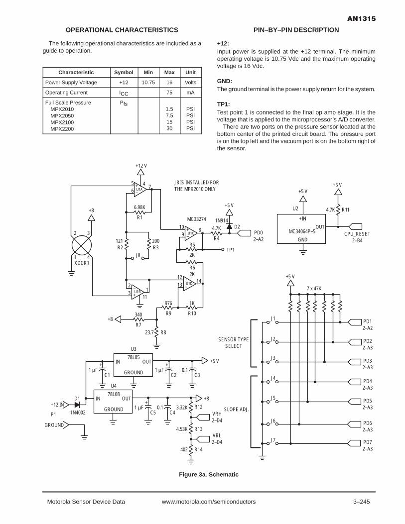
3–245Motorola Sensor Device Data www.motorola.com/semiconductors
OPERATIONAL CHARACTERISTICS
The following operational characteristics are included as aguide to operation.
Characteristic Symbol Min Max Unit
Power Supply Voltage +12 10.75 16 Volts
Operating Current ICC 75 mA
Full Scale PressureMPX2010MPX2050MPX2100MPX2200
Pfs1.57.51530
PSIPSIPSIPSI
PIN–BY–PIN DESCRIPTION
+12:Input power is supplied at the +12 terminal. The minimumoperating voltage is 10.75 Vdc and the maximum operatingvoltage is 16 Vdc.
GND:The ground terminal is the power supply return for the system.
TP1:Test point 1 is connected to the final op amp stage. It is thevoltage that is applied to the microprocessor’s A/D converter.
There are two ports on the pressure sensor located at thebottom center of the printed circuit board. The pressure portis on the top left and the vacuum port is on the bottom right ofthe sensor.
–+
–+
–+
+–
PD12–A2
PD22–A3
PD32–A3
PD42–A3
PD52–A3
PD62–A3
PD72–A3
+12 IN
GROUND
P1 1N4002
D1
1 µF+
C1
U4
78L08IN OUT
GROUND
U3
78L05IN OUT
GROUND 1 µF+
0.1C2 C3
+5 V
+8
R12
R13
R14
VRH2–D4
VRL2–D4
402
3.32K1 µF+
C50.1
C4
CPU_RESET2–B4
MC34064P–5
+IN
GND
OUT
U2
+5 V+5 V
R114.7K
PD02–A2
TP1
+5 V
1N914
4.7K
R4
8109
R5
2K
R62K
1412
13
U1A
U1C
U1D
U1B32
111
976
R9
1K
R10340
R7R823.7
+8
+8
1 4
2 3
XDCR1
121R2
200R3
6.98K
R1
56
47
+12 V
MC33274
D2
+5 V
7 x 47K
J1
J2
J3
J4
J5
J6
J7
SENSOR TYPESELECT
SLOPE ADJ.
Figure 3a. Schematic
J8 IS INSTALLED FORTHE MPX2010 ONLY
J8
4.53K

3–246 Motorola Sensor Device Datawww.motorola.com/semiconductors
02
17
65
43
02
17
65
43
20
4947
4842
4344
4546
3937
3832
3334
3536
17
65
43
3129
3024
2526
2728
2837
365
67
3435
831
329
1011
2930
1226
2713
1415
2425
1622
2317
1819
201
21
BLK
PLN
PIN
S:2–
4, 3
3, 3
8–40
C7
C8
22 p
F
22 p
F17
R15
10M
OSC
2
OSC
116
4.00
MH
z
Y1
POR
TAPO
RTB
POR
TC
U5
MC
68H
C70
5B5
PD0
PD1
PD2
PD3
PD4
PD5
PD6
PD7
PD0
PD1
PD2
PD1
PD4
PD5
PD6
PD7
1-C
2
1-E3
1-E3
1-E3
1-E3
1-E4
1-E4
1-E4
14 13 12 11 9 5 4 3
IRQ
*R
ESET
*VP
P6VD
DVS
STC
AP1
D/A
RD
ITD
OVR
LVR
HPL
MA
TCAP
2
1918
1510
4122
2321
5052
78
20
+5 V
CPU
_RES
ET1-
E2
0.1
C6
VRL
1-C
4VR
H1-
C4
LCD
1
Figure 3b. Schematic

3–247Motorola Sensor Device Data www.motorola.com/semiconductors
OPERATION
Connect the system to a 12 Vdc regulated power supply.(Note the polarity marked on the power terminal P1.)Depending on the particular pressure sensor being used withthe system, wire jumpers J1 through J3 and J8 must beinstalled at board assembly time. If at some later time it isdesirable to change the type of sensor that is installed on theboard, jumpers J1 through J3 and J8, must be reconfigured forthe system to function properly (see Table 1). If an invalid J1through J3 jumper combination (i.e., not listed in Table 1) isused the LCD will display “SE” to indicate that condition.These jumpers are read by the software and are used todetermine which sensor is installed on the board. Wire jumperJ8 is installed only when an MPX2010DP pressure sensor isused on the system. The purpose of wire jumper J8 will beexplained later in the text. Jumpers J4 through J7 are read bythe software to allow the user to adjust the slope constant usedfor the engineering units calculation (see Table 3). Thepressure and vacuum ports on the sensor must be left opento atmosphere anytime the board is powered–up. This isbecause the zero pressure offset voltage is computed atpower–up.
When you apply power to the system, the LCD will displayCAL for approximately 5 seconds. After that time, pressure orvacuum may be applied to the sensor. The system will thenstart displaying the applied pressure in PSI.
Table 3.
J7 J6 J5 J4 Action
IN IN IN IN Normal SlopeIN IN IN OUT Decrease the Slope Approximately 7%IN IN OUT IN Decrease the Slope Approximately 6%IN IN OUT OUT Decrease the Slope Approximately 5%IN OUT IN IN Decrease the Slope Approximately 4%IN OUT IN OUT Decrease the Slope Approximately 3%IN OUT OUT IN Decrease the Slope Approximately 2%IN OUT OUT OUT Decrease the Slope Approximately 1%
OUT IN IN IN Increase the Slope Approximately 1%OUT IN IN OUT Increase the Slope Approximately 2%OUT IN OUT IN Increase the Slope Approximately 3%OUT IN OUT OUT Increase the Slope Approximately 4%OUT OUT IN IN Increase the Slope Approximately 5%OUT OUT IN OUT Increase the Slope Approximately 6%OUT OUT OUT IN Increase the Slope Approximately 7%OUT OUT OUT OUT Normal Slope
To improve the accuracy of the system, you can change theconstant used by the program that determines the span of thesensor and amplifier. You will need an accurate test gauge(using PSI as the reference) to measure the pressure appliedto the sensor. Anytime after the display has completed thezero calculation, (after CAL is no longer displayed) apply thesensor’s full scale pressure (see Table 1), to the sensor. Makesure that jumpers J4 through J7 are in the “normal”configuration (see Table 3). Referring to Table 3, you canbetter “calibrate” the system by changing the configuration ofJ4 through J7. To “calibrate” the system, compare the displayreading against that of the test gauge (with J4 through J7 in the
“normal slope” configuration). Change the configuration of J4through J7 according to Table 3 to obtain the best results. Thecalibration jumpers may be changed while the system ispowered up as they are read by the software before eachdisplay update.
DESIGN CONSIDERATIONS
To build a system that will show how to interface anMPX2000 series pressure sensor to a microprocessor, thereare two main challenges. The first is to take a small differentialsignal produced by the sensor and produce a groundreferenced signal of sufficient amplitude to drive amicroprocessor’s A/D input. The second challenge is tounderstand the microprocessor’s operation and to writesoftware that makes the system function.
From a hardware point of view, the microprocessor portionof the system is straight forward. The microprocessor needspower, a clock source (crystal Y1, two capacitors and aresistor), and a reset signal to make it function. As for the A/Dconverter, external references are required to make it function.In this case, the power source for the sensor is divided toproduce the voltage references for the A/D converter.Accurate results will be achieved since the output from thesensor and the A/D references are ratiometric to its powersupply voltage.
The liquid crystal display is driven by Ports A, B and C of themicroprocessor. There are enough I/O lines on these ports toprovide drive for three full digits, the backplane and twodecimal points. Software routines provide the AC waveformnecessary to drive the display.
The analog portion of the system consists of the pressuresensor, a quad operational amplifier and the voltagereferences for the microprocessor’s A/D converter and signalconditioning circuitry. Figure 4 shows an interface circuit thatwill provide a single ended signal with sufficient amplitude todrive the microprocessor’s A/D input. It uses a quadoperational amplifier and several resistors to amplify and levelshift the sensor’s output. It is necessary to level shift the outputfrom the final amplifier into the A/D. Using single powersupplied op amps, the VCE saturation of the output from an opamp cannot be guaranteed to pull down to zero volts. Theanalog design shown here will provide a signal to the A/Dconverter with a span of approximately 4 volts when zero tofull–scale pressure is applied to the sensor. The finalamplifier’s output is level shifted to approximately 0.7 volts.This will provide a signal that will swing betweenapproximately 0.7 volts and 4.7 volts. The offset of 0.7 volts inthis implementation does not have to be trimmed to an exactpoint. The software will sample the voltage applied to the A/Dconverter at initial power up time and call that value “zero”. Theimportant thing to remember is that the span of the signal willbe approximately 4 volts when zero to full scale pressure isapplied to the sensor. The 4 volt swing in signal may varyslightly from sensor to sensor and can also vary due to resistortolerances in the analog circuitry. Jumpers J4 through J7 maybe placed in various configurations to compensate for thesevariations (see Table 3).

3–248 Motorola Sensor Device Datawww.motorola.com/semiconductors
–+
–+
–+
+–
PD0
TP1
+5 V
1N914
4.7K
R4
8109
R5
2K
R62K
1412
13
U1A
U1C
U1D
U1B32
111
976
R9
1K
R10340
R7R823.7
+8
+8
1 4
2 3
XDCR1
121R2
200R3
6.98K
R1
56
47
+12 V
MC33274D2
J8 IS INSTALLED FORTHE MPX2010 ONLY
J8
Figure 3. Figure 4. Analog Interface
Referring to Figure 4, most of the amplification of the voltagefrom the pressure sensor is provided by U1A which isconfigured as a differential amplifier. U1B serves as a unitygain buffer in order to keep any current that flows through R2(and R3) from being fed back into the sensor’s negativeoutput. With zero pressure applied to the sensor, thedifferential voltage from pin 2 to pin 4 of the sensor is zero orvery close to zero volts. The common mode, or the voltagemeasured between pins 2 or 4 to ground, is equal toapproximately one half of the voltage applied to the sensor, or4 volts. The zero pressure output voltage at pin 7 of U1A willthen be 4 volts because pin 1 of U1B is also at 4 volts, creatinga zero bias between pins 5 and 6 of U1A. The four volt zeropressure output will then be level shifted to the desired zeropressure offset voltage (approximately 0.7 volts) by U1C andU1D.
To further explain the operation of the level shifting circuitry,refer again to Figure 4. Assuming zero pressure is applied tothe sensor and the common mode voltage from the sensor is4 volts, the voltage applied to pin 12 of U1D will be 4 volts,implying pin 13 will be at 4 volts. The gain of amplifier U1D willbe (R10/(R8+R9)) +1 or a gain of 2. R7 will inject a Voffset (0.7volts) into amplifier U1D, thus causing the output at U1D pin14 to be 7.3 = (4 volts @ U1D pin 12 2) – 0.7 volts. The gainof U1C is also set at 2 ((R5/R6)+1). With 4 volts applied to pin10 of U1C, its output at U1C pin 8 will be 0.7 = ((4 volts @ U1Cpin 10 2) – 7.3 volts). For this scheme to work properly,amplifiers U1C and U1D must have a gain of 2 and the outputof U1D must be shifted down by the Voffset provided by R7. Inthis system, the 0.7 volts Voffset was arbitrarily picked andcould have been any voltage greater than the Vsat of the opamp being used. The system software will take in account any
variations of Voffset as it assumes no pressure is applied to thesensor at system power up.
The gain of the analog circuit is approximately 117. With thevalues shown in Figure 4, the gain of 117 will provide a spanof approximately 4 volts on U1C pin 8 when the pressuresensor and the 8 volt fixed voltage regulator are at theirmaximum output voltage tolerance. All of the sensors listed inTable 1 with the exception of the MPX2010DP outputapproximately 33 mV when full scale pressure is applied.When the MPX2010DP sensor is used, its full scale sensordifferential output is approximately 20 mV. J8 must be installedto increase the gain of the analog circuit to still provide the 4volts span out of U1C pin 8 with a 20 mV differential from thesensor.
Diode D2 is used to protect the microprocessor’s A/D inputif the output from U1C exceeds 5.6 volts. R4 is used to providecurrent limiting into D4 under failure or overvoltage conditions.
SOFTWARE
The source code, compiled listing, and S–record output forthe software used in this system are available on the MotorolaFreeware Bulletin Board Service in the MCU directory underthe filename DEVB158.ARC. To access the bulletin board,you must have a telephone line, a 300, 1200 or 2400 baudmodem and a personal computer. The modem must becompatible with the Bell 212A standard. Call (512) 891–3733to access the Bulletin Board Service.
Figure 5 is a flowchart for the program that controls thesystem. The software for the system consists of a number ofmodules. Their functions provide the capability for systemcalibration as well as displaying the pressure input to theMPX2000 series pressure sensor.

3–249Motorola Sensor Device Data www.motorola.com/semiconductors
Figure 5. DEVB–158 Software Flowchart
TIMERINTERRUPT
SERVICE TIMER REGISTERSSETUP COUNTER FOR NEXT INTERRUPT
SERVICE LIQUID CRYSTAL DISPLAY
RETURN
ACCUMULATE 100 A/D CONVERSIONSCOMPUTE INPUT PRESSURE
CONVERT TO DECIMAL/SEGMENT DATAPLACE IN RESULT OUTPUT BUFFER
COMPUTE SLOPE CONSTANT
INITIALIZE DISPLAY I/O PORTSINITIALIZE TIMER REGISTERS
DETERMINE SENSOR TYPEENABLE INTERRUPTS
START
The “C” compiler used in this project was provided by BYTECRAFT LTD. (519) 888–6911. A compiler listing of theprogram is included at the end of this document. The followingis a brief explanation of the routines:
delay() Used to provide a software loop delay.
read_a2d() Performs 100 reads on the A/D converter onmultiplexer channel 0 and returns the accumulation.
fixcompare() Services the internal timer for 15 ms. timercompare interrupts.
TIMERCMP() Alternates the data and backplane inputs tothe liquid crystal display.
initio() Sets up the microprocessor’s I/O ports, timer andenables processor interrupts.
adzero() This routine is called at powerup time. It delaysto let the power supply and the transducer stabilize. It thencalls “read_atod()” and saves the returned value as thesensors output voltage with zero pressure applied.
cvt_bin_dec(unsigned long arg) This routine convertsthe unsigned binary argument passed in “arg” to a five
digit decimal number in an array called “digit.” It then usesthe decimal results for each digit as an index into a tablethat converts the decimal number into a segment patternfor the display. This is then output to the display.
display_psi() This routine is called from “main()” never toreturn. The A/D converter routine is called, the pressureis calculated based on the type sensor detected and thepressure applied to the sensor is displayed. The loopthen repeats.
sensor_type() This routine determines the type of sensorfrom reading J1 to J3, setting the full scale pressure forthat particular sensor in a variable for use by display_psi().
sensor_slope() This routine determines the slopeconstant to be used by display_psi() for engineering unitsoutput.
main() This is the main routine called from reset. It calls“initio()” to setup the system’s I/O. “display_psi()” is calledto compute and display the pressure applied to thesensor.

3–250 Motorola Sensor Device Datawww.motorola.com/semiconductors
6805 ’C’ COMPILER V3.48 16–Oct–1991 PAGE 1
#pragma option f0;/*
THE FOLLOWING ’C’ SOURCE CODE IS WRITTEN FOR THE DEVB158 EVALUATIONBOARD. IT WAS COMPILED WITH A COMPILER COURTESY OF:
BYTE CRAFT LTD.421 KING ST.WATERLOO, ONTARIOCANADA N2J 4E4(519)888–6911
SOME SOURCE CODE CHANGES MAY BE NECESSARY FOR COMPILATION WITH OTHERCOMPILERS.
BILL LUCAS 2/5/92MOTOROLA, SPS
Revision historyrev. 1.0 initial release 3/19/92rev. 1.1 added additional decimal digit to the MPX2010 sensor. Originallyresolved the output to .1 PSI. Modified cvt_bin_dec to output PSI resolvedto .01 PSI. WLL 9/25/92
*/0800 1700 #pragma memory ROMPROG [5888] @ 0x0800 ;0050 0096 #pragma memory RAMPAGE0 [150] @ 0x0050 ;
/* Vector assignments */1FFE #pragma vector __RESET @ 0x1ffe ;1FFC #pragma vector __SWI @ 0x1ffc ;1FFA #pragma vector IRQ @ 0x1ffa ;1FF8 #pragma vector TIMERCAP @ 0x1ff8 ;1FF6 #pragma vector TIMERCMP @ 0x1ff6 ;1FF4 #pragma vector TIMEROV @ 0x1ff4 ;1FF2 #pragma vector SCI @ 0x1ff2 ;
#pragma has STOP ;#pragma has WAIT ;#pragma has MUL ;
/* Register assignments for the 68HC705B5 microcontroller */0000 #pragma portrw porta @ 0x00; /* */0001 #pragma portrw portb @ 0x01; /* */0002 #pragma portrw portc @ 0x02; /* */0003 #pragma portrw portd @ 0x03; /* in ,– ,SS ,SCK ,MOSI ,MISO,TxD,RxD */0004 #pragma portrw ddra @ 0x04; /* Data direction, Port A */0005 #pragma portrw ddrb @ 0x05; /* Data direction, Port B */0006 #pragma portrw ddrc @ 0x06; /* Data direction, Port C (all output) */0007 #pragma portrw eeclk @ 0x07; /* eeprom/eclk cntl */0008 #pragma portrw addata @ 0x08; /* a/d data register */0009 #pragma portrw adstat @ 0x09; /* a/d stat/control */000A #pragma portrw plma @ 0x0a; /* pulse length modulation a */000B #pragma portrw plmb @ 0x0b; /* pulse length modulation b */000C #pragma portrw misc @ 0x0c; /* miscellaneous register */000D #pragma portrw scibaud @ 0x0d; /* sci baud rate register */000E #pragma portrw scicntl1 @ 0x0e; /* sci control 1 */000F #pragma portrw scicntl2 @ 0x0f; /* sci control 2 */0010 #pragma portrw scistat @ 0x10; /* sci status reg */0011 #pragma portrw scidata @ 0x11; /* SCI Data */0012 #pragma portrw tcr @ 0x12; /* ICIE,OCIE,TOIE,0;0,0,IEGE,OLVL */0013 #pragma portrw tsr @ 0x13; /* ICF,OCF,TOF,0; 0,0,0,0 */0014 #pragma portrw icaphi1 @ 0x14; /* Input Capture Reg (Hi–0x14, Lo–0x15) */0015 #pragma portrw icaplo1 @ 0x15; /* Input Capture Reg (Hi–0x14, Lo–0x15) */0016 #pragma portrw ocmphi1 @ 0x16; /* Output Compare Reg (Hi–0x16, Lo–0x17) */0017 #pragma portrw ocmplo1 @ 0x17; /* Output Compare Reg (Hi–0x16, Lo–0x17) */0018 #pragma portrw tcnthi @ 0x18; /* Timer Count Reg (Hi–0x18, Lo–0x19) */0019 #pragma portrw tcntlo @ 0x19; /* Timer Count Reg (Hi–0x18, Lo–0x19) */001A #pragma portrw aregnthi @ 0x1A; /* Alternate Count Reg (Hi–$1A, Lo–$1B) */001B #pragma portrw aregntlo @ 0x1B; /* Alternate Count Reg (Hi–$1A, Lo–$1B) */001C #pragma portrw icaphi2 @ 0x1c; /* Input Capture Reg (Hi–0x1c, Lo–0x1d) */001D #pragma portrw icaplo2 @ 0x1d; /* Input Capture Reg (Hi–0x1c, Lo–0x1d) */001E #pragma portrw ocmphi2 @ 0x1e; /* Output Compare Reg (Hi–0x1e, Lo–0x1f) */001F #pragma portrw ocmplo2 @ 0x1f; /* Output Compare Reg (Hi–0x1e, Lo–0x1f) */

3–251Motorola Sensor Device Data www.motorola.com/semiconductors
1EFE 74 #pragma mor @ 0x1efe = 0x74; /* this disables the watchdog counter and doesnot add pull–down resistors on ports B and C */
/* put constants and variables here...they must be global *//***************************************************************************/
0800 FC 30 DA 7A 36 6E E6 38 FE const char lcdtab[]=0xfc,0x30,0xda,0x7a,0x36,0x6e,0xe6,0x38,0xfe,0x3e ;0809 3E
/* lcd pattern table 0 1 2 3 4 5 6 7 8 9 */
080A 27 10 03 E8 00 64 00 0A const long dectable[] = 10000, 1000, 100, 10 ;
0050 0005 unsigned int digit[5]; /* buffer to hold results from cvt_bin_dec function */
0812 00 96 00 4B 00 96 00 1E 00 const long type[] = 150, 75, 150, 30, 103 ;081B 67
/* MPX2010 MPX2050 MPX2100 MPX2200 MPX2700The table above will cause the final results of the pressure toengineering units to display the 1.5, 7.3 and 15.0 devices with adecimal place in the tens position. The 30 and 103 psi devices willdisplay in integer units.*/
const long slope_const[]= 450,418,423,427,432,436,441,445,454,459,081C 01 C2 01 A2 01 A7 01 AB 01 463,468,472,477,481,450 ;0825 B0 01 B4 01 B9 01 BD 01 C6 082E 01 CB 01 CF 01 D4 01 D8 01 0837 DD 01 E1 01 C2
0000 registera areg; /* processor’s A register */
0055 long atodtemp; /* temp to accumulate 100 a/d readings for smoothing */
0059 long slope; /* multiplier for adc to engineering units conversion */
005B int adcnt; /* a/d converter loop counter */
005C long xdcr_offset; /* initial xdcr offset */
005E long sensor_model; /* installed sensor based on J1..J3 */0060 int sensor_index; /* determine the location of the decimal pt. */
0061 0063 unsigned long i,j; /* counter for loops */
0065 unsigned int k; /* misc variable */
struct bothbytes int hi; int lo;;
union isboth0066 0002 long l;0066 0002 struct bothbytes b;0066 0002 ;
0066 0002 union isboth q; /* used for timer set–up */
/***************************************************************************/
/* variables for add32 */0068 0004 unsigned long SUM[2]; /* result */006C 0004 unsigned long ADDEND[2]; /* one input */0070 0004 unsigned long AUGEND[2]; /* second input */
/* variables for sub32 */0074 0004 unsigned long MINUE[2]; /* minuend */0078 0004 unsigned long SUBTRA[2]; /* subtrahend */007C 0004 unsigned long DIFF[2]; /* difference */
/* variables for mul32 */0080 0004 unsigned long MULTP[2]; /* multiplier */0084 0004 unsigned long MTEMP[2]; /* high order 4 bytes at return */0088 0004 unsigned long MULCAN[2]; /* multiplicand at input, low 4 bytes at return */

3–252 Motorola Sensor Device Datawww.motorola.com/semiconductors
/* variables for div32 */008C 0004 unsigned long DVDND[2]; /* Dividend */0090 0004 unsigned long DVSOR[2]; /* Divisor */0094 0004 unsigned long QUO[2]; /* Quotient */0098 unsigned int CNT; /* Loop counter */
/* The code starts here */
/***************************************************************************/
void add32()#asm
*––––––––––––––––––––––––––––––––––––––––––––––––––––––––––––––––––––––––––––** Add two 32–bit values.* Inputs:* ADDEND: ADDEND[0..3] HIGH ORDER BYTE IS ADDEND+0* AUGEND: AUGEND[0..3] HIGH ORDER BYTE IS AUGEND+0* Output:* SUM: SUM[0..3] HIGH ORDER BYTE IS SUM+0*––––––––––––––––––––––––––––––––––––––––––––––––––––––––––––––––––––––––––––**
083C B6 6F LDA ADDEND+3 low byte083E BB 73 ADD AUGEND+30840 B7 6B STA SUM+30842 B6 6E LDA ADDEND+2 medium low byte0844 B9 72 ADC AUGEND+20846 B7 6A STA SUM+20848 B6 6D LDA ADDEND+1 medium high byte084A B9 71 ADC AUGEND+1084C B7 69 STA SUM+1084E B6 6C LDA ADDEND high byte0850 B9 70 ADC AUGEND0852 B7 68 STA SUM0854 81 RTS done
*#endasm
0855 81 RTS
void sub32()#asm
*––––––––––––––––––––––––––––––––––––––––––––––––––––––––––––––––––––––––––––** Subtract two 32–bit values.* Input:* Minuend: MINUE[0..3]* Subtrahend: SUBTRA[0..3]* Output:* Difference: DIFF[1..0]*––––––––––––––––––––––––––––––––––––––––––––––––––––––––––––––––––––––––––––**
0856 B6 77 LDA MINUE+3 low byte0858 B0 7B SUB SUBTRA+3085A B7 7F STA DIFF+3085C B6 76 LDA MINUE+2 medium low byte085E B2 7A SBC SUBTRA+20860 B7 7E STA DIFF+20862 B6 75 LDA MINUE+1 medium high byte0864 B2 79 SBC SUBTRA+10866 B7 7D STA DIFF+10868 B6 74 LDA MINUE high byte086A B2 78 SBC SUBTRA086C B7 7C STA DIFF086E 81 RTS done
*#endasm
086F 81 RTS
void mul32()#asm
*––––––––––––––––––––––––––––––––––––––––––––––––––––––––––––––––––––––––––––** Multiply 32–bit value by a 32–bit value*** Input:

3–253Motorola Sensor Device Data www.motorola.com/semiconductors
* Multiplier: MULTP[0..3]* Multiplicand: MULCAN[0..3]* Output:* Product: MTEMP[0..3] AND MULCAN[0..3] MTEMP[0] IS THE HIGH* ORDER BYTE AND MULCAN[3] IS THE LOW ORDER BYTE** THIS ROUTINE DOES NOT USE THE MUL INSTRUCTION FOR THE SAKE OF USERS NOT* USING THE HC(7)05 SERIES PROCESSORS.*––––––––––––––––––––––––––––––––––––––––––––––––––––––––––––––––––––––––––––***
0870 AE 20 LDX #32 loop counter0872 3F 84 CLR MTEMP clean–up for result0874 3F 85 CLR MTEMP+1 *0876 3F 86 CLR MTEMP+2 *0878 3F 87 CLR MTEMP+3 *087A 36 88 ROR MULCAN low but to carry, the rest one to the right087C 36 89 ROR MULCAN+1 *087E 36 8A ROR MULCAN+2 *0880 36 8B ROR MULCAN+3 *0882 24 18 MNEXT BCC ROTATE if carry is set, do the add0884 B6 87 LDA MTEMP+3 *0886 BB 83 ADD MULTP+3 *0888 B7 87 STA MTEMP+3 *088A B6 86 LDA MTEMP+2 *088C B9 82 ADC MULTP+2 *088E B7 86 STA MTEMP+2 *0890 B6 85 LDA MTEMP+1 *0892 B9 81 ADC MULTP+1 *0894 B7 85 STA MTEMP+1 *0896 B6 84 LDA MTEMP *0898 B9 80 ADC MULTP *089A B7 84 STA MTEMP *089C 36 84 ROTATE ROR MTEMP else: shift low bit to carry, the rest to the right089E 36 85 ROR MTEMP+1 *08A0 36 86 ROR MTEMP+2 *08A2 36 87 ROR MTEMP+3 *08A4 36 88 ROR MULCAN *08A6 36 89 ROR MULCAN+1 *08A8 36 8A ROR MULCAN+2 *08AA 36 8B ROR MULCAN+3 *08AC 5A DEX bump the counter down08AD 26 D3 BNE MNEXT done yet ?08AF 81 RTS done
#endasm08B0 81 RTS
void div32()#asm
**––––––––––––––––––––––––––––––––––––––––––––––––––––––––––––––––––––––––––––** Divide 32 bit by 32 bit unsigned integer routine** Input:* Dividend: DVDND [+0..+3] HIGH ORDER BYTE IS DVND+0* Divisor: DVSOR [+0..+3] HIGH ORDER BYTE IS DVSOR+0* Output:* Quotient: QUO [+0..+3] HIGH ORDER BYTE IS QUO+0*––––––––––––––––––––––––––––––––––––––––––––––––––––––––––––––––––––––––––––**
08B1 3F 94 CLR QUOzero result registers08B3 3F 95 CLR QUO+1 *08B5 3F 96 CLR QUO+2 *08B7 3F 97 CLR QUO+3 *08B9 A6 01 LDA #1 initial loop count08BB 3D 90 TST DVSOR if the high order bit is set..no need to shift DVSOR08BD 2B 0F BMI DIV153
*08BF 4C DIV151 INCA bump the loop counter08C0 38 93 ASL DVSOR+3 now shift the divisor until the high order bit = 108C2 39 92 ROL DVSOR+208C4 39 91 ROL DVSOR+1 *08C6 39 90 ROL DVSOR *08C8 2B 04 BMI DIV153 done if high order bit = 1

3–254 Motorola Sensor Device Datawww.motorola.com/semiconductors
08CA A1 21 CMP #33 have we shifted all possible bits in the DVSOR yet ?08CC 26 F1 BNE DIV151 no
*08CE B7 98 DIV153 STA CNT save the loop counter so we can do the divide
*08D0 B6 8F DIV163 LDA DVDND+3 sub 32 bit divisor from dividend08D2 B0 93 SUB DVSOR+3 *08D4 B7 8F STA DVDND+3 *08D6 B6 8E LDA DVDND+2 *08D8 B2 92 SBC DVSOR+2 *08DA B7 8E STA DVDND+2 *08DC B6 8D LDA DVDND+1 *08DE B2 91 SBC DVSOR+1 *08E0 B7 8D STA DVDND+1 *08E2 B6 8C LDA DVDND *08E4 B2 90 SBC DVSOR *08E6 B7 8C STA DVDND *08E8 24 1B BCC DIV165 carry is clear if DVSOR was larger than DVDND
*08EA B6 8F LDA DVDND+3 add the divisor back...was larger than the dividend08EC BB 93 ADD DVSOR+3 *08EE B7 8F STA DVDND+3 *08F0 B6 8E LDA DVDND+2 *08F2 B9 92 ADC DVSOR+2 *08F4 B7 8E STA DVDND+2 *08F6 B6 8D LDA DVDND+1 *08F8 B9 91 ADC DVSOR+1 *08FA B7 8D STA DVDND+1 *08FC B6 8C LDA DVDND *08FE B9 90 ADC DVSOR *0900 B7 8C STA DVDND *0902 98 CLC this will clear the respective bit in QUO due to
* the need to add DVSOR back to DVND0903 20 01 BRA DIV1670905 99 DIV165 SEC this will set the respective bit in QUO0906 39 97 DIV167 ROL QUO+3 set or clear the low order bit in QUO based on above0908 39 96 ROL QUO+2 *090A 39 95 ROL QUO+1 *090C 39 94 ROL QUO *090E 34 90 LSR DVSOR divide the divisor by 20910 36 91 ROR DVSOR+1 *0912 36 92 ROR DVSOR+2 *0914 36 93 ROR DVSOR+3 *0916 3A 98 DEC CNT bump the loop counter down0918 26 B6 BNE DIV163 finished yet ?091A 81 RTSyes
*#endasm
091B 81 RTS
/***************************************************************************/
/* These interrupts are not used...give them a graceful return if forsome reason one occurs */
1FFC 09 1C __SWI()091C 80 RTI 1FFA 09 1D IRQ()091D 80 RTI 1FF8 09 1E TIMERCAP()091E 80 RTI 1FF4 09 1F TIMEROV()091F 80 RTI 1FF2 09 20 SCI()0920 80 RTI
/***************************************************************************/
void sensor_type()
0921 B6 03 LDA $03 k = portd & 0x0e; /* we only care about bits 1..3 */0923 A4 0E AND #$0E 0925 B7 65 STA $65 0927 34 65 LSR $65 k = k >> 1; /* right justify the variable */0929 B6 65 LDA $65 if ( k > 4 )092B A1 04 CMP #$04

3–255Motorola Sensor Device Data www.motorola.com/semiconductors
092D 23 0C BLS $093B /* we have a set–up error in wire jumpers J1 – J3 */
092F 3F 02 CLR $02 portc = 0; /* */0931 A6 6E LDA #$6E portb = 0x6e; /* S */0933 B7 01 STA $01 0935 A6 CE LDA #$CE porta = 0xce; /* E */0937 B7 00 STA $00 0939 20 FE BRA $0939 while(1);
093B B6 65 LDA $65 sensor_index = k;093D B7 60 STA $60 093F 97 TAX sensor_model = type[k];0940 58 LSLX 0941 D6 08 12 LDA $0812,X 0944 B7 5E STA $5E 0946 D6 08 13 LDA $0813,X 0949 B7 5F STA $5F 094B 81 RTS
/***************************************************************************/
void sensor_slope()
094C B6 03 LDA $03 k=portd & 0xf0; /* we only care about bits 4..7 */094E A4 F0 AND #$F0 0950 B7 65 STA $65 0952 34 65 LSR $65 k = k >> 4; /* right justify the variable */0954 34 65 LSR $65 0956 34 65 LSR $65 0958 34 65 LSR $65 095A BE 65 LDX $65 slope = slope_const[k];095C 58 LSLX 095D D6 08 1C LDA $081C,X 0960 B7 59 STA $59 0962 D6 08 1D LDA $081D,X 0965 B7 5A STA $5A 0967 81 RTS
/***************************************************************************/
void delay(void) /* just hang around for a while */
0968 3F 62 CLR $62 for (i=0; i<20000; ++i);096A 3F 61 CLR $61 096C B6 62 LDA $62 096E A0 20 SUB #$20 0970 B6 61 LDA $61 0972 A2 4E SBC #$4E 0974 24 08 BCC $097E 0976 3C 62 INC $62 0978 26 02 BNE $097C 097A 3C 61 INC $61 097C 20 EE BRA $096C 097E 81 RTS
/***************************************************************************/
read_a2d(void)/* read the a/d converter on channel 5 and accumulate the resultin atodtemp */
097F 3F 56 CLR $56 atodtemp=0; /* zero for accumulation */0981 3F 55 CLR $55 0983 3F 5B CLR $5B for ( adcnt = 0 ; adcnt<100; ++adcnt) /* do 100 a/d conversions */0985 B6 5B LDA $5B 0987 A8 80 EOR #$80 0989 A1 E4 CMP #$E4 098B 24 21 BCC $09AE
098D A6 20 LDA #$20 adstat = 0x20; /* convert on channel 0 */098F B7 09 STA $09 0991 0F 09 FD BRCLR 7,$09,$0991 while (!(adstat & 0x80)); /* wait for a/d to complete */0994 B6 08 LDA $08 atodtemp = addata + atodtemp;0996 3F 57 CLR $57 0998 B7 58 STA $58

3–256 Motorola Sensor Device Datawww.motorola.com/semiconductors
099A BB 56 ADD $56 099C B7 58 STA $58 099E B6 57 LDA $57 09A0 B9 55 ADC $55 09A2 B7 57 STA $57 09A4 B7 55 STA $55 09A6 B6 58 LDA $58 09A8 B7 56 STA $56
09AA 3C 5B INC $5B 09AC 20 D7 BRA $0985 09AE B6 56 LDA $56 atodtemp = atodtemp/100;09B0 B7 58 STA $58 09B2 B6 55 LDA $55 09B4 B7 57 STA $57 09B6 3F 9A CLR $9A 09B8 A6 64 LDA #$64 09BA B7 9B STA $9B 09BC CD 0B F1 JSR $0BF1 09BF CD 0C 22 JSR $0C22 09C2 BF 55 STX $55 09C4 B7 56 STA $56 09C6 81 RTS return atodtemp;
/***************************************************************************/
void fixcompare (void) /* sets–up the timer compare for the next interrupt */
09C7 B6 18 LDA $18 q.b.hi =tcnthi;09C9 B7 66 STA $66 09CB B6 19 LDA $19 q.b.lo = tcntlo;09CD B7 67 STA $67 09CF AB 4C ADD #$4C q.l +=7500; /* ((4mhz xtal/2)/4) = counter period = 2us.*7500 = 15ms. */09D1 B7 67 STA $67 09D3 B6 66 LDA $66 09D5 A9 1D ADC #$1D 09D7 B7 66 STA $66 09D9 B7 16 STA $16 ocmphi1 = q.b.hi;09DB B6 13 LDA $13 areg=tsr; /* dummy read */09DD B6 67 LDA $67 ocmplo1 = q.b.lo;09DF B7 17 STA $17 09E1 81 RTS
/***************************************************************************/
void TIMERCMP (void) /* timer service module */1FF6 09 E2 09E2 33 02 COM $02 portc =~ portc; /* service the lcd by inverting the ports */09E4 33 01 COM $01 portb =~ portb;09E6 33 00 COM $00 porta =~ porta;09E8 AD DD BSR $09C7 fixcompare();09EA 80 RTI
/***************************************************************************/
void adzero(void) /* called by initio() to save initial xdcr’s zeropressure offset voltage output */
09EB 3F 64 CLR $64 for ( j=0; j<20; ++j) /* give the sensor time to ”warm–up” and the09ED 3F 63 CLR $63 09EF B6 64 LDA $64 09F1 A0 14 SUB #$14 09F3 B6 63 LDA $63 09F5 A2 00 SBC #$00 09F7 24 0B BCC $0A04
power supply time to settle down */
09F9 CD 09 68 JSR $0968 delay();
09FC 3C 64 INC $64 09FE 26 02 BNE $0A02 0A00 3C 63 INC $63 0A02 20 EB BRA $09EF 0A04 CD 09 7F JSR $097F xdcr_offset = read_a2d();

3–257Motorola Sensor Device Data www.motorola.com/semiconductors
0A07 3F 5C CLR $5C 0A09 B7 5D STA $5D 0A0B 81 RTS
/***************************************************************************/
void initio (void) /* setup the I/O */
0A0C A6 20 LDA #$20 adstat = 0x20; /* power–up the A/D */0A0E B7 09 STA $09 0A10 3F 02 CLR $02 porta = portb = portc = 0;0A12 3F 01 CLR $01 0A14 3F 00 CLR $00 0A16 A6 FF LDA #$FF ddra = ddrb = ddrc = 0xff;0A18 B7 06 STA $06 0A1A B7 05 STA $05 0A1C B7 04 STA $04 0A1E B6 13 LDA $13 areg=tsr; /* dummy read */0A20 3F 1E CLR $1E ocmphi1 = ocmphi2 = 0;0A22 3F 16 CLR $16 0A24 B6 1F LDA $1F areg = ocmplo2; /* clear out output compare 2 if it happens to be set */0A26 AD 9F BSR $09C7 fixcompare(); /* set–up for the first timer interrupt */0A28 A6 40 LDA #$40 tcr = 0x40;0A2A B7 12 STA $12 0A2C 9A CLI CLI; /* let the interrupts begin ! */
/* write CAL to the display */0A2D A6 CC LDA #$CC portc = 0xcc; /* C */0A2F B7 02 STA $02 0A31 A6 BE LDA #$BE portb = 0xbe; /* A */0A33 B7 01 STA $01 0A35 A6 C4 LDA #$C4 porta = 0xc4; /* L */0A37 B7 00 STA $00 0A39 CD 09 21 JSR $0921 sensor_type(); /* get the model of the sensor based on J1..J3 */0A3C AD AD BSR $09EB adzero(); /* auto zero */0A3E 81 RTS
/***************************************************************************/
void cvt_bin_dec(unsigned long arg)
/* First converts the argument to a five digit decimal value. The msd is inthe lowest address. Then leading zero suppress the value and write it to thedisplay ports.
The argument value is 0..65535 decimal. */
009D 0A3F BF 9D STX $9D 0A41 B7 9E STA $9E 009F char i;00A0 unsigned long l;0A43 3F 9F CLR $9F for ( i=0; i < 5; ++i )0A45 B6 9F LDA $9F 0A47 A1 05 CMP #$05 0A49 24 07 BCC $0A52
0A4B 97 TAX digit[i] = 0x0; /* put blanks in all digit positions */0A4C 6F 50 CLR $50,X
0A4E 3C 9F INC $9F 0A50 20 F3 BRA $0A45 0A52 3F 9F CLR $9F for ( i=0; i < 4; ++i )0A54 B6 9F LDA $9F 0A56 A1 04 CMP #$04 0A58 24 7A BCC $0AD4
0A5A 97 TAX if ( arg >= dectable [i] )0A5B 58 LSLX 0A5C D6 08 0B LDA $080B,X 0A5F B0 9E SUB $9E 0A61 B7 58 STA $58 0A63 B6 9D LDA $9D 0A65 A8 80 EOR #$80 0A67 B7 57 STA $57 0A69 D6 08 0A LDA $080A,X 0A6C A8 80 EOR #$80 0A6E B2 57 SBC $57

3–258 Motorola Sensor Device Datawww.motorola.com/semiconductors
0A70 BA 58 ORA $58 0A72 22 5C BHI $0AD0
0A74 BE 9F LDX $9F l = dectable[i];0A76 58 LSLX 0A77 D6 08 0A LDA $080A,X 0A7A B7 A0 STA $A0 0A7C D6 08 0B LDA $080B,X 0A7F B7 A1 STA $A1 0A81 B6 9E LDA $9E digit[i] = arg / l;0A83 B7 58 STA $58 0A85 B6 9D LDA $9D 0A87 B7 57 STA $57 0A89 B6 A0 LDA $A0 0A8B B7 9A STA $9A 0A8D B6 A1 LDA $A1 0A8F B7 9B STA $9B 0A91 CD 0B F1 JSR $0BF1 0A94 CD 0C 22 JSR $0C22 0A97 BF 57 STX $57 0A99 B7 58 STA $58 0A9B BE 9F LDX $9F 0A9D E7 50 STA $50,X 0A9F BE 9F LDX $9F arg = arg–(digit[i] * l);0AA1 E6 50 LDA $50,X 0AA3 3F 57 CLR $57 0AA5 B7 58 STA $58 0AA7 B6 A0 LDA $A0 0AA9 B7 9A STA $9A 0AAB B6 A1 LDA $A1 0AAD B7 9B STA $9B 0AAF CD 0B D2 JSR $0BD2 0AB2 BF 57 STX $57 0AB4 B7 58 STA $58 0AB6 33 57 COM $57 0AB8 30 58 NEG $58 0ABA 26 02 BNE $0ABE 0ABC 3C 57 INC $57 0ABE B6 58 LDA $58 0AC0 BB 9E ADD $9E 0AC2 B7 58 STA $58 0AC4 B6 57 LDA $57 0AC6 B9 9D ADC $9D 0AC8 B7 57 STA $57 0ACA B7 9D STA $9D 0ACC B6 58 LDA $58 0ACE B7 9E STA $9E
0AD0 3C 9F INC $9F 0AD2 20 80 BRA $0A54 0AD4 B6 9E LDA $9E digit[i] = arg;0AD6 B7 58 STA $58 0AD8 B6 9D LDA $9D 0ADA B7 57 STA $57 0ADC BE 9F LDX $9F 0ADE B6 58 LDA $58 0AE0 E7 50 STA $50,X
/* now zero suppress and send the lcd pattern to the display */0AE2 9B SEI SEI;0AE3 3D 52 TST $52 if ( digit[2] == 0 ) /* leading zero suppression */0AE5 26 04 BNE $0AEB 0AE7 3F 02 CLR $02 portc = 0;0AE9 20 07 BRA $0AF2 else0AEB BE 52 LDX $52 portc = ( lcdtab[digit[2]] ); /* 100’s digit */0AED D6 08 00 LDA $0800,X 0AF0 B7 02 STA $02 0AF2 3D 52 TST $52 if ( digit[2] == 0 && digit[3] == 0 )0AF4 26 08 BNE $0AFE 0AF6 3D 53 TST $53 0AF8 26 04 BNE $0AFE 0AFA 3F 01 CLR $01 portb=0;0AFC 20 07 BRA $0B05 else0AFE BE 53 LDX $53 portb = ( lcdtab[digit[3]] ); /* 10’s digit */0B00 D6 08 00 LDA $0800,X

3–259Motorola Sensor Device Data www.motorola.com/semiconductors
0B03 B7 01 STA $01 0B05 BE 54 LDX $54 porta = ( lcdtab[digit[4]] ); /* 1’s digit */0B07 D6 08 00 LDA $0800,X 0B0A B7 00 STA $00
/* place the decimal point only if the sensor is 15 psi or 7.5 psi */0B0C B6 60 LDA $60 if ( sensor_index < 3 )0B0E A8 80 EOR #$80 0B10 A1 83 CMP #$83 0B12 24 08 BCC $0B1C 0B14 BE 54 LDX $54 porta = ( lcdtab[digit[4]]+1 ); /* add the decimal point to the lsd */0B16 D6 08 00 LDA $0800,X 0B19 4C INCA 0B1A B7 00 STA $00 0B1C 3D 60 TST $60 if(sensor_index ==0) /* special case */0B1E 26 0F BNE $0B2F
0B20 BE 54 LDX $54 porta = ( lcdtab[digit[4]] ); /* get rid of the decimal at lsd */0B22 D6 08 00 LDA $0800,X 0B25 B7 00 STA $00 0B27 BE 53 LDX $53 portb = ( lcdtab[digit[3]]+1 ); /* decimal point at middle digit */0B29 D6 08 00 LDA $0800,X 0B2C 4C INCA 0B2D B7 01 STA $01
0B2F 9A CLI CLI;0B30 CD 09 68 JSR $0968 delay();0B33 81 RTS
/****************************************************************/
void display_psi(void)/*
At power–up it is assumed that the pressure or vacuum port ofthe sensor is open to atmosphere. The code in initio() delaysfor the sensor and power supply to stabilize. One hundred A/Dconversions are averaged. That result is called xdcr_offset.This routine calls the A/D routine which performs one hundredconversions, divides the result by 100 and returns the value.If the value returned is less than or equal to the xdcr_offset,the value of xdcr_offset is substituted. If the value returnedis greater than xdcr_offset, xdcr_offset is subtracted from thereturned value.
*/
while(1)
0B34 CD 09 7F JSR $097F atodtemp = read_a2d(); /* atodtemp = raw a/d ( 0..255 ) */0B37 3F 55 CLR $55 0B39 B7 56 STA $56 0B3B B0 5D SUB $5D if ( atodtemp <= xdcr_offset )0B3D B7 58 STA $58 0B3F B6 5C LDA $5C 0B41 A8 80 EOR #$80 0B43 B7 57 STA $57 0B45 B6 55 LDA $55 0B47 A8 80 EOR #$80 0B49 B2 57 SBC $57 0B4B BA 58 ORA $58 0B4D 22 08 BHI $0B57 0B4F B6 5C LDA $5C atodtemp = xdcr_offset;0B51 B7 55 STA $55 0B53 B6 5D LDA $5D 0B55 B7 56 STA $56 0B57 B6 56 LDA $56 atodtemp –= xdcr_offset; /* remove the offset */0B59 B0 5D SUB $5D 0B5B B7 56 STA $56 0B5D B6 55 LDA $55 0B5F B2 5C SBC $5C 0B61 B7 55 STA $55 0B63 CD 09 4C JSR $094C sensor_slope(); /* establish the slope constant for this output */0B66 B6 56 LDA $56 atodtemp *= sensor_model;0B68 B7 58 STA $58 0B6A B6 55 LDA $55 0B6C B7 57 STA $57 0B6E B6 5E LDA $5E

3–260 Motorola Sensor Device Datawww.motorola.com/semiconductors
0B70 B7 9A STA $9A 0B72 B6 5F LDA $5F 0B74 B7 9B STA $9B 0B76 CD 0B D2 JSR $0BD2 0B79 BF 55 STX $55 0B7B B7 56 STA $56 0B7D 3F 89 CLR $89 MULTP[0] = MULCAN[0] = 0;0B7F 3F 88 CLR $88 0B81 3F 81 CLR $81 0B83 3F 80 CLR $80 0B85 9F TXA MULTP[1] = atodtemp;0B86 B7 82 STA $82 0B88 B6 56 LDA $56 0B8A B7 83 STA $83 0B8C B6 59 LDA $59 MULCAN[1] = slope;0B8E B7 8A STA $8A 0B90 B6 5A LDA $5A 0B92 B7 8B STA $8B 0B94 CD 08 70 JSR $0870 mul32(); /* analog value * slope based on J1 through J3 */0B97 3F 90 CLR $90 DVSOR[0] = 1; /* now divide by 100000 */0B99 A6 01 LDA #$01 0B9B B7 91 STA $91 0B9D A6 86 LDA #$86 DVSOR[1] = 0x86a0;0B9F B7 92 STA $92 0BA1 A6 A0 LDA #$A0 0BA3 B7 93 STA $93 0BA5 B6 88 LDA $88 DVDND[0] = MULCAN[0];0BA7 B7 8C STA $8C 0BA9 B6 89 LDA $89 0BAB B7 8D STA $8D 0BAD B6 8A LDA $8A DVDND[1] = MULCAN[1];0BAF B7 8E STA $8E 0BB1 B6 8B LDA $8B 0BB3 B7 8F STA $8F 0BB5 CD 08 B1 JSR $08B1 div32();0BB8 B6 96 LDA $96 atodtemp = QUO[1]; /* convert to psi */0BBA B7 55 STA $55 0BBC B6 97 LDA $97 0BBE B7 56 STA $56 0BC0 BE 55 LDX $55 cvt_bin_dec( atodtemp ); /* convert to decimal and display */0BC2 CD 0A 3F JSR $0A3F 0BC5 CC 0B 34 JMP $0B34 0BC8 81 RTS
/***************************************************************************/
void main()
0BC9 CD 0A 0C JSR $0A0C initio(); /* set–up the processor’s i/o */0BCC CD 0B 34 JSR $0B34 display_psi();0BCF 20 FE BRA $0BCF while(1); /* should never get back to here */0BD1 81 RTS 0BD2 BE 58 LDX $58 0BD4 B6 9B LDA $9B 0BD6 42 MUL 0BD7 B7 A4 STA $A4 0BD9 BF A5 STX $A5 0BDB BE 57 LDX $57 0BDD B6 9B LDA $9B 0BDF 42 MUL 0BE0 BB A5 ADD $A5 0BE2 B7 A5 STA $A5 0BE4 BE 58 LDX $58 0BE6 B6 9A LDA $9A 0BE8 42 MUL 0BE9 BB A5 ADD $A5 0BEB B7 A5 STA $A5 0BED 97 TAX 0BEE B6 A4 LDA $A4 0BF0 81 RTS 0BF1 3F A4 CLR $A4 0BF3 5F CLRX 0BF4 3F A2 CLR $A2 0BF6 3F A3 CLR $A3 0BF8 5C INCX 0BF9 38 58 LSL $58

3–261Motorola Sensor Device Data www.motorola.com/semiconductors
0BFB 39 57 ROL $57 0BFD 39 A2 ROL $A2 0BFF 39 A3 ROL $A3 0C01 B6 A2 LDA $A2 0C03 B0 9B SUB $9B 0C05 B7 A2 STA $A2 0C07 B6 A3 LDA $A3 0C09 B2 9A SBC $9A 0C0B B7 A3 STA $A3 0C0D 24 0D BCC $0C1C 0C0F B6 9B LDA $9B 0C11 BB A2 ADD $A2 0C13 B7 A2 STA $A2 0C15 B6 9A LDA $9A 0C17 B9 A3 ADC $A3 0C19 B7 A3 STA $A3 0C1B 99 SEC 0C1C 59 ROLX 0C1D 39 A4 ROL $A4 0C1F 24 D8 BCC $0BF9 0C21 81 RTS 0C22 53 COMX 0C23 9F TXA 0C24 BE A4 LDX $A4 0C26 53 COMX 0C27 81 RTS 1FFE 0B C9
SYMBOL TABLE
LABEL VALUE LABEL VALUE LABEL VALUE LABEL VALUE
ADDEND 006C | AUGEND 0070 | CNT 0098 | DIFF 007C DIV151 08BF | DIV153 08CE | DIV163 08D0 | DIV165 0905 DIV167 0906 | DVDND 008C | DVSOR 0090 | IRQ 091D MINUE 0074 | MNEXT 0882 | MTEMP 0084 | MULCAN 0088 MULTP 0080 | QUO 0094 | ROTATE 089C | SCI 0920 SUBTRA 0078 | SUM 0068 | TIMERCAP 091E | TIMERCMP 09E2 TIMEROV 091F | __LDIV 0BF1 | __LongIX 009A | __MAIN 0BC9 __MUL 0000 | __MUL16x16 0BD2 | __RDIV 0C22 | __RESET 1FFE __STARTUP 0000 | __STOP 0000 | __SWI 091C | __WAIT 0000 __longAC 0057 | adcnt 005B | add32 083C | addata 0008 adstat 0009 | adzero 09EB | aregnthi 001A | aregntlo 001B arg 009D | atodtemp 0055 | b 0000 | bothbytes 0002 cvt_bin_dec 0A3F | ddra 0004 | ddrb 0005 | ddrc 0006 dectable 080A | delay 0968 | digit 0050 | display_psi 0B34 div32 08B1 | eeclk 0007 | fixcompare 09C7 | hi 0000 i 0061 | icaphi1 0014 | icaphi2 001C | icaplo1 0015 icaplo2 001D | initio 0A0C | isboth 0002 | j 0063 k 0065 | l 0000 | lcdtab 0800 | lo 0001 main 0BC9 | misc 000C | mul32 0870 | ocmphi1 0016 ocmphi2 001E | ocmplo1 0017 | ocmplo2 001F | plma 000A plmb 000B | porta 0000 | portb 0001 | portc 0002 portd 0003 | q 0066 | read_a2d 097F | scibaud 000D scicntl1 000E | scicntl2 000F | scidata 0011 | scistat 0010 sensor_index 0060 | sensor_model 005E | sensor_slope 094C | sensor_type 0921 slope 0059 | slope_const 081C | sub32 0856 | tcnthi 0018 tcntlo 0019 | tcr 0012 | tsr 0013 | type 0812 xdcr_offset 005C |
MEMORY USAGE MAP (’X’ = Used, ’–’ = Unused)
0800 : XXXXXXXXXXXXXXXX XXXXXXXXXXXXXXXX XXXXXXXXXXXXXXXX XXXXXXXXXXXXXXXX0840 : XXXXXXXXXXXXXXXX XXXXXXXXXXXXXXXX XXXXXXXXXXXXXXXX XXXXXXXXXXXXXXXX0880 : XXXXXXXXXXXXXXXX XXXXXXXXXXXXXXXX XXXXXXXXXXXXXXXX XXXXXXXXXXXXXXXX08C0 : XXXXXXXXXXXXXXXX XXXXXXXXXXXXXXXX XXXXXXXXXXXXXXXX XXXXXXXXXXXXXXXX
0900 : XXXXXXXXXXXXXXXX XXXXXXXXXXXXXXXX XXXXXXXXXXXXXXXX XXXXXXXXXXXXXXXX0940 : XXXXXXXXXXXXXXXX XXXXXXXXXXXXXXXX XXXXXXXXXXXXXXXX XXXXXXXXXXXXXXXX0980 : XXXXXXXXXXXXXXXX XXXXXXXXXXXXXXXX XXXXXXXXXXXXXXXX XXXXXXXXXXXXXXXX09C0 : XXXXXXXXXXXXXXXX XXXXXXXXXXXXXXXX XXXXXXXXXXXXXXXX XXXXXXXXXXXXXXXX
0A00 : XXXXXXXXXXXXXXXX XXXXXXXXXXXXXXXX XXXXXXXXXXXXXXXX XXXXXXXXXXXXXXXX0A40 : XXXXXXXXXXXXXXXX XXXXXXXXXXXXXXXX XXXXXXXXXXXXXXXX XXXXXXXXXXXXXXXX0A80 : XXXXXXXXXXXXXXXX XXXXXXXXXXXXXXXX XXXXXXXXXXXXXXXX XXXXXXXXXXXXXXXX0AC0 : XXXXXXXXXXXXXXXX XXXXXXXXXXXXXXXX XXXXXXXXXXXXXXXX XXXXXXXXXXXXXXXX
3–262 Motorola Sensor Device Datawww.motorola.com/semiconductors
0B00 : XXXXXXXXXXXXXXXX XXXXXXXXXXXXXXXX XXXXXXXXXXXXXXXX XXXXXXXXXXXXXXXX0B40 : XXXXXXXXXXXXXXXX XXXXXXXXXXXXXXXX XXXXXXXXXXXXXXXX XXXXXXXXXXXXXXXX0B80 : XXXXXXXXXXXXXXXX XXXXXXXXXXXXXXXX XXXXXXXXXXXXXXXX XXXXXXXXXXXXXXXX0BC0 : XXXXXXXXXXXXXXXX XXXXXXXXXXXXXXXX XXXXXXXXXXXXXXXX XXXXXXXXXXXXXXXX
0C00 : XXXXXXXXXXXXXXXX XXXXXXXXXXXXXXXX XXXXXXXX–––––––– ––––––––––––––––0C40 : –––––––––––––––– –––––––––––––––– –––––––––––––––– ––––––––––––––––0C80 : –––––––––––––––– –––––––––––––––– –––––––––––––––– ––––––––––––––––0CC0 : –––––––––––––––– –––––––––––––––– –––––––––––––––– ––––––––––––––––
1E00 : –––––––––––––––– –––––––––––––––– –––––––––––––––– ––––––––––––––––1E40 : –––––––––––––––– –––––––––––––––– –––––––––––––––– ––––––––––––––––1E80 : –––––––––––––––– –––––––––––––––– –––––––––––––––– ––––––––––––––––1EC0 : –––––––––––––––– –––––––––––––––– –––––––––––––––– ––––––––––––––X–
1F00 : –––––––––––––––– –––––––––––––––– –––––––––––––––– ––––––––––––––––1F40 : –––––––––––––––– –––––––––––––––– –––––––––––––––– ––––––––––––––––1F80 : –––––––––––––––– –––––––––––––––– –––––––––––––––– ––––––––––––––––1FC0 : –––––––––––––––– –––––––––––––––– –––––––––––––––– ––XXXXXXXXXXXXXX
All other memory blocks unused.
Errors : 0Warnings : 0

3–263Motorola Sensor Device Data www.motorola.com/semiconductors
Prepared by: Jeff BaumDiscrete Applications Engineering
INTRODUCTION
Typically, a semiconductor pressure transducer convertsapplied pressure to a “low–level” voltage signal. Currenttechnology enables this sensor output to be temperaturecompensated and amplified to higher voltage levels on asingle silicon integrated circuit (IC). While on–chiptemperature compensation and signal conditioning certainlyprovide a significant amount of added value to the basicsensing device, one must also consider how this final outputwill be used and/or interfaced for further processing. In mostsensing systems, the sensor signal will be input to additionalanalog circuitry, control logic, or a microcontroller unit (MCU).
MCU–based systems have become extremely costeffective. The level of intelligence which can be obtained foronly a couple of dollars, or less, has made relatively simple8–bit microcontrollers the partner of choice for semiconductorpressure transducers. In order for the sensor to communicateits pressure–dependent voltage signal to the microprocessor,the MCU must have an analog–to–digital converter (A/D) asan on–chip resource or an additional IC packaged A/D. In the
latter case, the A/D must have a communications interfacethat is compatible with one of the MCU’s communicationsprotocols. MCU’s are adept at detecting logic–level transitionsthat occur at input pins designated for screening such events.As an alternative to the conventional A/D sensor/MCUinterface, one can measure either a period (frequency) orpulse width of an incoming square or rectangular wave signal.Common MCU timer subsystem clock frequencies permittemporal measurements with resolution of hundreds ofnanoseconds. Thus, one is capable of accurately measuringthe the frequency output of a device that is interfaced to sucha timer channel. If sensors can provide a frequency modulatedsignal that is linearly proportional to the applied pressurebeing measured, then an accurate, inexpensive (no A/D)MCU–based sensor system is a viable solution to manychallenging sensing applications. Besides the inherent costsavings of such a system, this design concept offers additionalbenefits to remote sensing applications and sensing inelectrically noisy environments.
Figure 1. DEVB160 Frequency Output Sensor EVB(Board No Longer Available)
SEMICONDUCTOR APPLICATION NOTE
REV 2

3–264 Motorola Sensor Device Datawww.motorola.com/semiconductors
The following sections will detail the design issues involvedin such a system architecture, and will provide an examplecircuit which has been developed as an evaluation tool forfrequency output pressure sensor applications.
DESIGN CONSIDERATIONS
Signal ConditioningMotorola’s MPX2000 Series sensors are temperature
compensated and calibrated – i.e. – offset and full–scale spanare precision trimmed – pressure transducers. These sensorsare available in full–scale pressure ranges from 10 kPa (1.5psi) to 200 kPa (30 psi). Although the specifications in the datasheets apply only to a 10 V supply voltage, the output of thesedevices is ratiometric with the supply voltage. At the absolutemaximum supply voltage specified, 16 V, the sensor willproduce a differential output voltage of 64 mV at the ratedfull–scale pressure of the given sensor. One exception to thisis that the full–scale span of the MPX2010 (10 kPa sensor) willbe only 40 mV due to a slightly lower sensitivity. Since themaximum supply voltage produces the most output voltage,it is evident that even the best case scenario will require somesignal conditioning to obtain a usable voltage level.
Many different “instrumentation–type” amplifier circuits cansatisfy the signal conditioning needs of these devices.Depending on the precision and temperature performancedemanded by a given application, one can design an amplifiercircuit using a wide variety of operational amplifier (op amp)IC packages with external resistors of various tolerances, ora precision–trimmed integrated instrumentation amplifier IC.In any case, the usual goal is to have a single–ended supply,“rail–to–rail” output (i.e. use as much of the range from groundto the supply voltage as possible, without saturating the opamps). In addition, one may need the flexibility of performingzero–pressure offset adjust and full–scale pressurecalibration. The circuitry or device used to accomplish thevoltage–to–frequency conversion will determine if, how, andwhere calibration adjustments are needed. See EvaluationBoard Circuit Description section for details.
Voltage–to–Frequency ConversionSince most semiconductor pressure sensors provide a
voltage output, one must have a means of converting thisvoltage signal to a frequency that is proportional to the sensoroutput voltage. Assuming the analog voltage output of thesensor is proportional to the applied pressure, the resultant
frequency will be linearly related to the pressure beingmeasured. There are many different timing circuits that canperform voltage–to–frequency conversion. Most of the“simple” (relatively low number of components) circuits do notprovide the accuracy or the stability needed for reliablyencoding a signal quantity. Fortunately, manyvoltage–to–frequency (V/F) converter IC’s are commerciallyavailable that will satisfy this function.
Switching Time ReductionOne limitation of some V/F converters is the less than
adequate switching transition times that effect the pulse orsquare–wave frequency signal. The required switching speedwill be determined by the hardware used to detect theswitching edges. The Motorola family of microcontrollers haveinput–capture functions that employ “Schmitt trigger–like”inputs with hysteresis on the dedicated input pins. In this case,slow rise and fall times will not cause an input capture pin tobe in an indeterminate state during a transition. Thus, CMOSlogic instability and significant timing errors will be preventedduring slow transitions. Since the sensor’s frequency outputmay be interfaced to other logic configurations, a designer’smain concern is to comply with a worst–case timing scenario.For high–speed CMOS logic, the maximum rise and fall timesare typically specified at several hundreds of nanoseconds.Thus, it is wise to speed up the switching edges at the outputof the V/F converter. A single small–signal FET and a resistorare all that is required to obtain switching times below 100 ns.
APPLICATIONS
Besides eliminating the need for an A/D converter, afrequency output is conducive to applications in which thesensor output must be transmitted over long distances, orwhen the presence of noise in the sensor environment is likelyto corrupt an otherwise healthy signal. For sensor outputsencoded as a voltage, induced noise from electromagneticfields will contaminate the true voltage signal. A frequencysignal has greater immunity to these noise sources and canbe effectively filtered in proximity to the MCU input. In otherwords, the frequency measured at the MCU will be thefrequency transmitted at the output of a sensor locatedremotely. Since high–frequency noise and 50–60 Hz linenoise are the two most prominent sources for contaminationof instrumentation signals, a frequency signal with a range inthe low end of the kHz spectrum is capable of being wellfiltered prior to being examined at the MCU.

3–265Motorola Sensor Device Data www.motorola.com/semiconductors
Table 1. Specifications
Characteristics Symbol Min Typ Max Units
Power Supply Voltage B+ 10 30 Volts
Full Scale Pressure PFS
– MPX2010 10 kPa
– MPX2050 50 kPa
– MPX2100 100 kPa
– MPX2200 200 kPa
Full Scale Output fFS 10 kHz
Zero Pressure Offset fOFF 1 kHz
Sensitivity SAOUT 9/PFS kHz/kPa
Quiescent Current ICC 55 mA
EVALUATION BOARD
The following sections present an example of the signalconditioning, including frequency conversion, that wasdeveloped as an evaluation tool for the Motorola MPX2000series pressure sensors. A summary of the informationrequired to use evaluation board number DEVB160 ispresented as follows.
DescriptionThe evaluation board shown in Figure 1 is designed to
transduce pressure, vacuum or differential pressure into asingle–ended, ground referenced voltage that is then input toa voltage–to–frequency converter. It nominally provides a 1kHz output at zero pressure and 10 kHz at full scale pressure.Zero pressure calibration is made with a trimpot that is locatedon the lower half of the left side of the board, while the full scaleoutput can be calibrated via another trimpot just above theoffset adjust. The board comes with an MPX2100DP sensorinstalled, but will accommodate any MPX2000 series sensor.One additional modification that may be required is that thegain of the circuit must be increased slightly when using anMPX2010 sensor. Specifically, the resistor R5 must beincreased from 7.5 kΩ to 12 kΩ.
Circuit DescriptionThe following pin description and circuit operation
corresponds to the schematic shown in Figure 2.
Pin–by–Pin Description
B+:Input power is supplied at the B+ terminal of connector CN1.
Minimum input voltage is 10 V and maximum is 30 V.
Fout :A logic–level (5 V) frequency output is supplied at the OUT
terminal (CN1). The nominal signal it provides is 1 kHz at zero
pressure and 10 kHz at full scale pressure. Zero pressurefrequency is adjustable and set with R12. Full–scalefrequency is calibrated via R13. This output is designed to bedirectly connected to a microcontroller timer systeminput–capture channel.
GND:The ground terminal on connector CN1 is intended for use
as the power supply return and signal common. Test pointterminal TP3 is also connected to ground, for measurementconvenience.
TP1:Test point 1 is connected to the final frequency output, Fout.
TP2:Test point 2 is connected to the +5 V regulator output. It can
be used to verify that this supply voltage is within its tolerance.
TP3:Test point 3 is the additional ground point mentioned above
in the GND description.
TP4:Test point 4 is connected to the +8 V regulator output. It can
be used to verify that this supply voltage is within its tolerance.
P1, P2:Pressure and Vacuum ports P1 and P2 protrude from the
sensor on the right side of the board. Pressure port P1 is onthe top (marked side of package) and vacuum port P2, ifpresent, is on the bottom. When the board is set up with a dualported sensor (DP suffix), pressure applied to P1, vacuumapplied to P2 or a differential pressure applied between thetwo all produce the same output voltage per kPa of input.Neither port is labeled. Absolute maximum differentialpressure is 700 kPa.

3–266M
otorola Sensor D
evice Data
ww
w.m
otorola.com/sem
iconductors
Figure 2. D
EV
B160 F
requency Output S
ensor Evaluation B
oard
S1
13
2
on/off
C11 Fµ
2
GROUND
IN OUT
MC78L08ACPU2
TP4
1
R8620
D1MV57124A
4U1AMC33274
U1C10
9 8
C40.1 Fµ
R112 k
11
2
3 +
–
R6120
R57.5 k
6
57
U1B
12
13
R102 k R13
1 k
R34.3 k
FULL–SCALE
C510 Fµ
+
TP3 TP1
GNDFB+
CN1
B+
+
U1D
R7820
R91 k
R41.5 k
1234
FoutLogComRt+V
VCtCt
V
8765
C30.01 Fµ
R21 k
2
3 1TP2
C60.1 Fµ
R1240
U5BS107A
X1MPX2100DP
4
1
23
C20.1 Fµ
AD654
GROUND
OUTIN
U4MC78L05ACP
3
1 +
–
R12200
OFFSET
–+
–
TANTALUM
123
14
Ω
Ω
ΩΩ
Ω Ω
Ω Ω
ΩΩ
Ω
Ω
out
in SS
CC
Ω

3–267Motorola Sensor Device Data www.motorola.com/semiconductors
The following is a table of the components that are assembled on the DEVB160 Frequency Output Sensor Evaluation Board.
Table 2. Parts List
Designators Quantity Description Manufacturer Part Number
C1 1 1 µF Capacitor
C2 1 0.1 µF Capacitor
C3 1 0.01 µF Capacitor
C4 1 0.1 µF Capacitor
C5 1 10 µF Cap+ tantalum
C6 1 0.1 µF Capacitor
CN1 1 .15LS 3 Term PHX Contact 1727023
D1 1 RED LED Quality Tech. MV57124A
R1 1 240 Ω resistor
R2, R9 2 1 kΩ resistor
R3 1 4.3 kΩ resistor
R4 1 1.5 kΩ resistor
R5 1 7.5 kΩ resistor
R6 1 120 Ω resistor
R7 1 820 Ω resistor
R8 1 620 Ω resistor
R10, R11 2 2 kΩ resistor
R12 1 200 Ω Trimpot Bourns 3386P–1–201
R13 1 1 kΩ Trimpot Bourns 3386P–1–102
S1 1 SPDT miniature switch NKK SS–12SDP2
TP1 1 YELLOW Testpoint Control Design TP–104–01–04
TP2 1 BLUE Testpoint Control Design TP–104–01–06
TP3 1 BLACK Testpoint Control Design TP–104–01–00
TP4 1 GREEN Testpoint Control Design TP–104–01–05
U1 1 Quad Op Amp Motorola MC33274
U2 1 8 V Regulator Motorola MC78L08ACP
U3 1 AD654 Analog Devices AD654
U4 1 5 V Regulator Motorola MC78L05ACP
U5 1 Small–Signal FET Motorola BS107A
X1 1 Pressure Sensor Motorola MPX2100DP
NOTE: All resistors are 1/4 watt, 5% tolerance values. All capacitors are 50 V rated, ±20% tolerance values.

3–268 Motorola Sensor Device Datawww.motorola.com/semiconductors
Circuit OperationThe voltage signal conditioning portion of this circuit is a
variation on the classic instrumentation amplifierconfiguration. It is capable of providing high differential gainand good common–mode rejection with very high inputimpedance; however, it provides a more user friendly methodof performing the offset/bias point adjustment. It uses four opamps and several resistors to amplify and level shift thesensor’s output. Most of the amplification is done in U1Awhich is configured as a differential amplifier. Unwantedcurrent flow through the sensor is prevented by buffer U1B. Atzero pressure the differential voltage from pin 2 to pin 4 on thesensor has been precision trimmed to essentially zero volts.The common–mode voltage on each of these nodes is 4 V(one–half the sensor supply voltage). The zero pressureoutput voltage at pin 1 of U1A is then 4.0 V, since any othervoltage would be coupled back to pin 2 via R5 and create anon–zero bias across U1A’s differential inputs. This 4.0 V zeropressure DC output voltage is then level translated to thedesired zero pressure offset voltage by U1C and U1D. Theoffset voltage is produced by R4 and adjustment trimpot R12.R7’s value is such that the total source impedance into pin 13is approximately 1 k. The gain is approximately (R5/R6)(1 +R11/R10), which is 125 for the values shown in Figure 2. Again of 125 is selected to provide a 4 V span for 32 mV offull–scale sensor output (at a sensor supply voltage of 8 V).
The resulting .5 V to 4.5 V output from U1C is thenconverted by the V/F converter to the nominal 1–10 kHz thathas been specified. The AD654 V/F converter receives theamplified sensor output at pin 8 of op amp U1C. The full–scalefrequency is determined by R3, R13 and C3 according to thefollowing formula:
Fout (full-scale)Vin
(10V)(R3R13)C3
For best performance, R3 and R13 should be chosen toprovide 1 mA of drive current at the full–scale voltageproduced at pin 3 of the AD654 (U3). The input stage of theAD654 is an op–amp; thus, it will work to make the voltage atpin 3 of U3 equal to the voltage seen at pin 4 of U3 (pins 3 and4 are the input terminals of the op amp). Since the amplifiedsensor output will be 4.5 V at full–scale pressure, R3 + R13should be approximately equal to 4.5 kΩ to have optimallinearity performance. Once the total resistance from pin 3 ofU3 to ground is set, the value of C3 will determine thefull–scale frequency output of the V/F. Trimpot R13 should besized (relative to R3 value) to provide the desired amount offull–scale frequency adjustment. The zero–pressurefrequency is adjusted via the offset adjust provided forcalibrating the offset voltage of the signal conditioned sensoroutput. For additional information on using this particular V/Fconverter, see the applications information provided in theAnalog Devices Data Conversion Products Databook.
The frequency output has its edge transitions “sped” up bya small–signal FET inverter. This final output is directlycompatible with microprocessor timer inputs, as well as any
other high–speed CMOS logic. The amplifier portion of thiscircuit has been patented by Motorola Inc. and was introducedon evaluation board DEVB150A. Additional informationpertaining to this circuit and the evaluation board DEVB150Ais contained in Motorola Application Note AN1313.1
TEST/CALIBRATION PROCEDURE
1. Connect a +12 V supply between B+ and GND terminalson the connector CN1.
2. Connect a frequency counter or scope probe on the Foutterminal of CN1 or on TP1 with the test instrumentationground clipped to TP3 or GND.
3 . Turn the power switch, S1, to the on position. PowerLED, D1, should be illuminated. Verify that the voltage atTP2 and TP4 (relative to GND or TP3) is 5 V and 8 V,respectively. While monitoring the frequency output bywhichever means one has chosen, one should see a50% duty cycle square wave signal.
4. Turn the wiper of the OFFSET adjust trimpot, R12, to theapproximate center of the pot.
5. Apply 100 kPa to pressure port P1 of the MPX2100DP(topside port on marked side of the package) sensor, X1.
6. Adjust the FULL–SCALE trimpot, R13, until the outputfrequency is 10 kHz. If 10 kHz is not within the trim rangeof the full–scale adjustment trimpot, tweak the offsetadjust trimpot to obtain 10 kHz (remember, the offset potwas at an arbitrary midrange setting as per step 4).
7. Apply zero pressure to the pressure port (i.e., both portsat ambient pressure, no differential pressure applied).Adjust OFFSET trimpot so frequency output is 1 kHz.
8. Verify that zero pressure and full–scale pressure(100 kPa) produce 1 and 10 kHz respectively, at Foutand/or TP1. A second iteration of adjustment on bothfull–scale and offset may be necessary to fine tune the1 – 10 kHz range.
CONCLUSION
Transforming conventional analog voltage sensor outputsto frequency has great utility for a variety of applications.Sensing remotely and/or in noisy environments is particularlychallenging for low–level (mV) voltage output sensors such asthe MPX2000 Series pressure sensors. Converting theMPX2000 sensor output to frequency is relatively easy toaccomplish, while providing the noise immunity required foraccurate pressure sensing. The evaluation board presentedis an excellent tool for either “stand–alone” evaluation of theMPX2000 Series pressure sensors or as a building block forsystem prototyping which can make use of DEVB160 as a“drop–in” frequency output sensor solution. The output of theDEVB160 circuit is ideally conditioned for interfacing to MCUtimer inputs that can measure the sensor frequency signal.
REFERENCES
1. Schultz, Warren (Motorola, Inc.), “Sensor Building BlockEvaluation Board,” Motorola Application Note AN1313.

3–269Motorola Sensor Device Data www.motorola.com/semiconductors
Prepared by: Warren SchultzDiscrete Applications Engineering
INTRODUCTION
The most popular silicon pressure sensors arepiezoresistive bridges that produce a differential outputvoltage in response to pressure applied to a thin silicondiaphragm. Output voltage for these sensors is generally 25to 50 mV full scale. Interface to microcomputers, therefore,generally involves gaining up the relatively small outputvoltage, performing a differential to single ended conversion,and scaling the analog signal into a range appropriate foranalog to digital conversion. Alternately, the analog pressuresignal can be converted to a frequency modulated 5 Vwaveform or 4–20 mA current loop, either of which is relativelyimmune to noise on long interconnect lines.
A variety of circuit techniques that address interface designare presented. Sensing amplifiers, analog to digitalconversion, frequency modulation and 4–20 mA current loopsare considered.
PRESSURE SENSOR BASICS
The essence of piezoresistive pressure sensors is theWheatstone bridge shown in Figure 1. Bridge resistors RP1,RP2, RV1 and RV2 are arranged on a thin silicon diaphragmsuch that when pressure is applied RP1 and RP2 increase invalue while RV1 and RV2 decrease a similar amount.Pressure on the diaphragm, therefore, unbalances the bridgeand produces a differential output signal. One of thefundamental properties of this structure is that the differentialoutput voltage is directly proportional to bias voltage B+. Thischaracteristic implies that the accuracy of the pressuremeasurement depends directly on the tolerance of the biassupply. It also provides a convenient means for temperaturecompensation. The bridge resistors are silicon resistors thathave positive temperature coefficients. Therefore, when theyare placed in series with zero TC temperature compensationresistors RC1 and RC2 the amount of voltage applied to thebridge increases with temperature. This increase in voltageproduces an increase in electrical sensitivity which offsets andcompensates for the negative temperature coefficientassociated with piezoresistance.
Since RC1 and RC2 are approximately equal, the outputvoltage common mode is very nearly fixed at 1/2 B+. In atypical MPX2100 sensor, the bridge resistors are nominally425 ohms; RC1 and RC2 are nominally 680 ohms. With thesevalues and 10 V applied to B+, a delta R of 1.8 ohms at fullscale pressure produces 40 mV of differential output voltage.
Figure 1. Sensor Equivalent Circuit
RETURN
B+
RC1
RV1
S+
RP1
RP2
RV2
S–
RC2
PRESSURE
INSTRUMENTATION AMPLIFIER INTERFACES
Instrumentation amplifiers are by far the most commoninterface circuits that are used with pressure sensors. Anexample of an inexpensive instrumentation amplifier basedinterface circuit is shown in Figure 2. It uses an MC33274 quadoperational amplifier and several resistors that are configuredas a classic instrumentation amplifier with one importantexception. In an instrumentation amplifier resistor R3 isnormally returned to ground. Returning R3 to ground sets theoutput voltage for zero differential input to 0 V DC. Formicrocomputer interface a positive offset voltage on the orderof 0.3 to 0.8 V is generally desired. Therefore, R3 is connectedto pin 14 of U1D which supplies a buffered offset voltage thatis derived from the wiper of R6. This voltage establishes a DCoutput for zero differential input. The translation is one to one.Within the tolerances of the circuit, whatever voltage appearsat the wiper of R6 will also appear as the zero pressure DCoffset voltage at the output.
With R10 at 240 ohms, gain is set for a nominal value of 125.This provides a 4 V span for 32 mV of full scale sensor output.Setting the offset voltage to .75 V results in a 0.75 V to 4.75 Voutput that is directly compatible with microprocessor A/Dinputs. Over a zero to 50° C temperature range, combinedaccuracy for an MPX2000 series sensor and this interface ison the order of ± 10%.
SEMICONDUCTOR APPLICATION NOTE
REV 1

3–270 Motorola Sensor Device Datawww.motorola.com/semiconductors
Figure 2. Instrumentation Amplifier Interface
B+
GND
C11 µF
C20.1 µF
C3 .001 µF
U2MC78L08ACP
U1BMC33274
I
GO
3
R77.5 k
R6
1 k1213
14
8
R2
1 k
R5R915 k
1 kU1AMC33274
R10240*
56
47
R41 k R3 1 k
U1CMC3327410
9
2
31
23
4 1
XDCR1MPX2000 SERIESPRESSURE SENSOR
OUTPUT
11
2
R8 15 k
+–
+–
+–
–+
U1DMC33274
* NOTE: FOR MPX2010, R10 = 150 OHMS
ZERO
1
For applications requiring greater precision a fullyintegrated instrument amplifier such as an LTC1100CN8 givesbetter results. In Figure 3 one of these amplifiers is used toprovide a gain of 100, as well as differential to single endedconversion. Zero offset is provided by dividing down theprecision reference to 0.5 V and buffering with U2B. Thisvoltage is fed into the LTC1100CN8’s ground pin which isequivalent to returning R3 to pin 14 of U1D in Figure 2. Anadditional non–inverting gain stage consisting of U2A, R1 andR2 is used to scale the sensor’s full scale span to 4 V. R2 isalso returned to the buffered .5 V to maintain the 0.5 V zerooffset that was established in the instrumentation amplifier.Output voltage range is therefore 0.5 to 4.5 V.
Both of these instrumentation amplifier circuits do theirintended job with a relatively straightforward tradeoff betweencost and performance. The circuit of Figure 2 has the usualcumulative tolerance problem that is associated withinstrumentation amplifiers that have discrete resistors, but ithas a relatively low cost. The integrated instrumentationamplifier in Figure 3 solves this problem with precisiontrimmed film resistors and also provides superior input offsetperformance. Component cost, however, is significantlyhigher.
SENSOR SPECIFIC INTERFACE AMPLIFIER
A low cost interface designed specifically for pressuresensors improves upon the instrumentation amplifier in Figure2. Shown in Figure 4, it uses one quad op amp and severalresistors to amplify and level shift the sensor’s output. Most ofthe amplification is done in U1A which is configured as adifferential amplifier. It is isolated from the sensor’s positiveoutput by U1B. The purpose of U1B is to prevent feedbackcurrent that flows through R5 and R6 from flowing into thesensor. At zero pressure the voltage from pin 2 to pin 4 on thesensor is 0 V. For example, let’s say that the common modevoltage on these pins is 4.0 V. The zero pressure outputvoltage at pin 1 of U1A is then 4.0 V, since any other voltagewould be coupled back to pin 2 via R6 and create a non–zerobias across U1A’s differential inputs. This 4.0 V zero pressureDC output voltage is then level translated to the desired zeropressure offset voltage (VOFFSET) by U1C and U1D.

3–271Motorola Sensor Device Data www.motorola.com/semiconductors
Figure 3. Precision Instrument Amplifier Interface
B+
C11µF 23
4 1
XDCR1MPX2000 SERIESPRESSURE SENSOR OUTPUT
NCNC
OUTTRM
NCVINVTGND
U1
1234
8765
MC1404
6
3
5
4
+
–
7
1 2
3+–
5
67
R41 k 1%
MC34072
U2BR210 k 1%
R16.04 k 1%
8U2A
C30.01 µF
U1
MC34072
R319.1 k 1%
C20.1 µF
LTC1100CN8
+–
1
4
Figure 4. Sensor Specific Interface Circuit
B+
GND
C11 µF
C20.1 µF
U2MC78L08ACP
U1AMC33274
I
GO
3
12
1314
8
U1BMC33274
R5120*
32
41
R4 1 k
U1CMC33274
109
6
57
23
4 1
XDCR1MPX2000 SERIESPRESSURESENSOR
OUTPUT
11
2
R6 7.5 k
+–
+–
+–
–+
* NOTE: FOR MPX2010, R5 = 75 OHMS
U1DMC33274R3
820
R1 2 k
R2 2 k
R9 200
ZEROCAL.
R81.5 k
1

3–272 Motorola Sensor Device Datawww.motorola.com/semiconductors
To see how the level translation works, let’s look at thesimplified schematic in Figure 5. Again assuming a commonmode voltage of 4.0 V, the voltage applied to pin 12 of U1D is4.0 V, implying that pin 13 is also at 4.0 V. This leaves 4.0 V– VOFFSET across R3, which is 3.5 V if VOFFSET is set to 0.5V. Since no current flows into pin 13, the same current flowsthrough both R3 and R4. With both of these resistors set to thesame value, they have the same voltage drop, implying a 3.5V drop across R4. Adding the voltages (0.5 + 3.5 + 3.5) yields
7.5 V at pin 14 of U1D. Similarly 4.0 V at pin 10 of U1C implies4.0 V at pin 9, and the drop across R2 is 7.5 V – 4.0 V = 3.5V. Again 3.5 V across R2 implies an equal drop across R1, andthe voltage at pin 8 is 4.0 V – 3.5 V = .5 V. For this DC outputvoltage to be independent of the sensor’s common modevoltage it is necessary to satisfy the condition that R4/R3 =R2/R1. In Figure 4, VOFFSET is produced by R8 andadjustment pot R9. R3’s value is adjusted such that the totalsource impedance into pin 13 is approximately 1 k.
Figure 5. Simplified Sensor Specific Interface
B+
GND
U1AMC33274
1213
14
8
U1BMC33274
R5120*
32
41
R4 1 k
U1CMC33274
109
6
57
23
4 1
XDCR1MPX2000 SERIESPRESSURESENSOR
OUTPUT
11
R6 7.5 k
+–
+–
+–
–+
*NOTE: FOR MPX2010, R5 = 75 OHMS
U1DMC33274R3
1 k
R1 2 k
R2 2 k
V
+8
OFFSET
Gain is approximately (R6/R5)(R1/R2+1), which is 125 forthe values shown in Figure 4. A gain of 125 is selected toprovide a 4 V span for the 32 mV of full scale sensor output thatis obtained with 8 V B+.
The resulting 0.5 V to 4.5 V output from U1C is preferableto the 0.75 to 4.75 V range developed by the instrumentamplifier configuration in Figure 2. It also uses fewer parts.This circuit does not have the instrument amplifier’spropensity for oscillation and therefore does not requirecompensation capacitor C3 that is shown in Figure 2. It alsorequires one less resistor, which in addition to reducingcomponent count also reduces accumulated tolerances dueto resistor variations.
This circuit as well as the instrumentation amplifier interfacesin Figures 2 and 3 is designed for direct connection to a
microcomputer A/D input. Using the MC68HC11 as anexample, the interface circuit output is connected to any of theE ports, such as port E0 as shown in Figure 6. To get maximumaccuracy from the A/D conversion, VREFH is tied to 4.85 V andVREFL is tied to 0.30 V by dividing down a 5 V reference with1% resistors.
SINGLE SLOPE A/D CONVERTER
The 8 bit A/D converters that are commonly available onchip in microcomputers are usually well suited to pressuresensing applications. In applications that require more than 8bits, the circuit in Figure 7 extends resolution to 11 bits with anexternal analog–to–digital converter. It also provides aninterface to digital systems that do not have an internal A/Dfunction.

3–273Motorola Sensor Device Data www.motorola.com/semiconductors
Figure 6. Application Example
RETURN
B+
RC1
RV1
S+
RP1
RP2
RV2
S–
RC2
BIAS
+
—
B+
INTERFACEAMPLIFIER
OUTPUT
GND
GND
VREFH
VREFL
+5 V
15.0 OHMS1%
30.1 OHMS1%
4.85 V
.302 V
453 OHMS1%
0
12
34
5
67
PORT E
MC68HC11
VSS
MPX2000SERIESPRESSURESENSOR
VS
Beginning with the ramp generator, a timing ramp isgenerated with current source U5 and capacitor C3.Initialization is provided by Q1 which sets the voltage on C3at approximately ground. With the values shown, 470 µAflowing into 0.47 µF provide approximately a 5 msec ramp timefrom zero to 5 V. Assuming zero pressure on the sensor, inputsto both comparators U2A and U2B are at the same voltage.Therefore, as the ramp voltage sweeps from zero to 5 V, bothPA0 and PA1 will go low at the same time when the rampvoltage exceeds the common mode voltage. The processorcounts the number of clock cycles between the time that PA0and PA1 go low, reading zero for zero pressure.
In this circuit, U4A and U4B form the front end of aninstrument amplifier. They differentially amplify the sensor’soutput. The resulting amplified differential signal is thensampled and held in U1 and U3. The sample and hold functionis performed in order to keep input data constant during theconversion process. The stabilized signals coming out of U1and U3 feed a higher output voltage to U2A than U2B,assuming that pressure is applied to the sensor. Therefore,the ramp will trip U2B before U2A is tripped, creating a timedifference between PA0 going low and PA1 going low. Theprocessor reads the number of clock cycles between thesetwo events. This number is then linearly scaled with softwareto represent the amplified output voltage, accomplishing theanalog to digital conversion.
When the ramp reaches the reference voltage establishedby R9 and R10, comparator U2C is tripped, and a resetcommand is generated. To accomplish reset, Q1 is turned on
with an output from PA7, and the sample and hold circuits aredelatched with an output from PB1. Resolution is limited byclock frequency and ramp linearity. With the ramp generatorshown in Figure 7 and a clock frequency of 2 MHz; resolutionis 11 bits.
From a software point of view, the A/D conversion consistsof latching the sample and hold, reading the value of themicrocomputer’s free running counter, turning off Q1, andwaiting for the three comparator outputs to change state fromlogic 1 to logic 0. The analog input voltage is determined bycounting, in 0.5 µsec steps, the number of clock cyclesbetween PA0 and PA1 going low.
LONG DISTANCE INTERFACES
In applications where there is a significant distance betweenthe sensor and microcomputer, two types of interfaces aretypically used. They are frequency output and 4–20 mA loops.In the frequency output topology, pressure is converted into azero to 5 V digital signal whose frequency varies linearly withpressure. A minimum frequency corresponds to zero pressureand above this, frequency output is determined by a Hz/unitpressure scaling factor. If minimizing the number of wires to aremote sensor is the most important design consideration,4–20 mA current loops are the topology of choice. These loopsutilize power and ground as the 4–20 mA signal line andtherefore require only two wires to the sensor. In this topology4 mA of total current drain from the sensor corresponds to zeropressure, and 20 mA to full scale.

3–274M
otorola Sensor D
evice Data
ww
w.m
otorola.com/sem
iconductors
+5
U4AMC33078
R2 402 k
NOTE:UNLESS OTHERWISE SPECIFIEDALL RESISTORS ARE 1% METAL FILM
413
8
7 6
U4BMC33078
R3 402 k
3
8
7 6
1 4U3
LF398A
U1
+
–
+
–
+
–
5
5 R8
22 k 5%
10
11
6
7
5
4
LM139A
LM139A
LM139A
U2B
U2D
U2A
1
2
13
+8.5 –8.5
+8.5 –8.5
LF398A
R7
22 k 5%
PA0
PB1
PA1
U5LM334Z-3 D1
1N914
R4147
R6
1.5 k 5%
R5
4.7
+10
Q1
2N7000
8
914
U2C
LM139A
R109.09 k
R91 k
+5
+
–
PA7
PA2
U7MC68HC11E9FN
C40.01 FµPOLYPROP
C50.01 FµPOLYPROPC1 22 pF
C2 22 pF
C30.47 Fµ
C70.1 Fµ
XDCR1MPX2000 SERIES
PRESSURE SENSORR5
120*1
23
4
43
21
11
65
+
–
+
–7
5%
Figure 7. S
ingle Slope A
/D C
onverter

3–275M
otorola Sensor D
evice Data
ww
w.m
otorola.com/sem
iconductors
* NOTE: FOR MPX2010, R8 = 75 OHMS
B+
GND
R6 2 k
R7 2 k
U2CMC33274
R1 1 kR2820
XDCR1MPX2000 SERIES
PRESSURE SENSOR
U2AMC33274
U2BMC33274
R4 7.5 k
1213 14
U2DMC33274
109
8
1
3
2
I
GO
C11 Fµ
R8120*
3
4
6 7
CT
CT
+VSV
RT –VS
COM
F
R114.3 k
5 2
R121 kFULL SCALE CAL.
1
R51.5 k
200R3
U1MC78L08ACP
C20.1 Fµ
1
3I
GO
Q1BS107A
2
R91 k
C3
0.01 Fµ
8
NOMINAL OUTPUT:
5 V
0
U3AD654
ZEROCAL.
U4MC78L05ACP
C40.1 Fµ
OUTPUT
R10240
OUT
IN
1 kHz @ ZERO PRESSURE10 kHz @ FULL SCALE
2
43
3 2
4 1
65
7
11
+–
–+
+–
–+
Figure 8. F
requency Output P
ressure Sensor

3–276 Motorola Sensor Device Datawww.motorola.com/semiconductors
A relatively straightforward circuit for converting pressure tofrequency is shown in Figure 8. It consists of three basic parts.The interface amplifier is the same circuit that was describedin Figure 4. Its 0.5 to 4.5 V output is fed directly into an AD654voltage–to–frequency converter. On the AD654, C3 setsnominal output frequency. Zero pressure output is calibratedto 1 kHz by adjusting the zero pressure input voltage with R3.Full scale adjustments are made with R12 which sets the fullscale frequency to 10 kHz. The output of the AD654 is then fedinto a buffer consisting of Q1 and R10. The buffer is used toclean up the edges and level translate the output to 5 V.Advantages of this approach are that the frequency output iseasily read by a microcomputer’s timer and transmission over
a twisted pair line is relatively easy. Where very long distancesare involved, the primary disadvantage is that 3 wires (VCC,ground and an output line) are routed to the sensor.
A 4–20 mA loop reduces the number of wires to two. Itsoutput is embedded in the VCC and ground lines as an activecurrent source. A straightforward way to apply this techniqueto pressure sensing is shown in Figure 9. In this figure anMPX7000 series high impedance pressure sensor is mated toan XTR101 4–20 mA two–wire transmitter. It is set up to pull4 mA from its power line at zero pressure and 20 mA at fullscale. At the receiving end a 240 ohm resistor referenced tosignal ground will provide a 0.96 to 4.8 V signal that is suitablefor microcomputer A/D inputs.
Figure 9. 4–20 mA Pressure Transducer
23
4 1
913
714
21
.96 – 4.8V
24 V
PLOOP240
RETURN
D11N4002
4–20 mA OUTPUT
R17501/2 W
Q1MPSA06
U1XTR101
XDCR1MPX7000SERIESSENSOR
D21N4565A6.4 V @ .5 mA
R330
R5100
SPAN
R6100 k
OFFSET
R41M
12
11
10 8
4
5
6
3
C10.01 µF
–
+
2 mA
+
–
R21 k
Bias for the sensor is provided by two 1 mA current sources(pins 10 and 11) that are tied in parallel and run into a 1N4565A6.4 V temperature compensated zener reference. Thesensor’s differential output is fed directly into XTR101’sinverting and non–inverting inputs. Zero pressure offset iscalibrated to 4 mA with R6. Biased with 6.4 V, the sensor’s fullscale output is 24.8 mV. Given this input R3 + R5 nominallytotal 64 ohms to produce the 16 mA span required for 20 mAfull scale. Calibration is set with R5.
The XTR101 requires that the differential input voltage at pins
3 and 4 has a common mode voltage between 4 and 6 V. Thesensor’s common mode voltage is one half its supply voltageor 3.2 V. R2 boosts this common mode voltage by1 k 2 mA or 2 V, establishing a common mode voltage for thetransmitter’s input of 5.2 V. To allow operation over a 12 to 40V range, dissipation is off–loaded from the IC by boosting theoutput with Q1 and R1. D1 is also included for protection. Itprohibits reverse polarity from causing damage. Advantages ofthis topology include simplicity and, of course, the two wireinterface.

3–277M
otorola Sensor D
evice Data
ww
w.m
otorola.com/sem
iconductors
123456728333435363738398
31329
10112930
12
26271314152425
16
22231718192021
40
PC0PC2PC1PC7PC6PC5PC4PC3
PB2PB1PB7PB6PB5PB4PB3
PA0PA2PA1PA7PA6PA5PA4PA3
1
2
3
XDCR1MPX5100
R4
4.7 k
R310 k
R210 k U2
MC34064P-5
J1 J2C122 pF R1
10 MY14 MHz
C222 pF
R615 %
R5453 %
R730.1 %
VRH VRLD/A
TCAP1
TCAP2
VDDPD0
PD1PD2PD3
VPP6
IRQ
PD5
RESET
PD6PD7
OSC1
OSC2
V RDI TDO
PD4
U1
MC68HC705B5FN
IEEE LCD 5657OR EQUIVALENT
LIQUIDCRYSTALDISPLAY
+5
SS
Figure 10. M
PX
5100 LCD
Pressure G
auge
3–278 Motorola Sensor Device Datawww.motorola.com/semiconductors
DIRECT INTERFACEWITH INTEGRATED SENSORS
The simplest interface is achieved with an integrated sensorand a microcomputer that has an on–chip A/D converter.Figure 10 shows an LCD pressure gauge that is made with anMPX5100 integrated sensor and MC68HC05 microcomputer.Although the total schematic is reasonably complicated, theinterface between the sensor and the micro is a single wire.The MPX5100 has an internal amplifier that outputs a 0.5 to4.5 V signal that inputs directly to A/D port PD5 on the HC05.
The software in this system is written such that theprocessor assumes zero pressure at power up, reads thesensor’s output voltage, and stores this value as zeropressure offset. Full scale span is adjustable with jumpers J1and J2. For this particular system the software is written suchthat with J1 out and J2 in, span is decreased by 1.5%. Similarlywith J1 in and J2 out, span is increased by 1.5%. Given the ±2.5% full scale spec on the sensor, these jumpers allowcalibration to ± 1% without the use of pots.
MIX AND MATCH
The circuits that have been described so far are intended tobe used as functional blocks. They may be combined in avariety of ways to meet the particular needs of an application.For example, the Frequency Output Pressure Sensor inFigure 8 uses the sensor interface circuit described in Figure4 to provide an input to the voltage–to–frequency converter.Alternately, an MPX5100 could be directly connected to pin 4of the AD654 or the output of Figure 3’s PrecisionInstrumentation Amplifier Interface could by substituted in thesame way. Similarly, the Pressure Gauge described in Figure10 could be constructed with any of the interfaces that havebeen described.
CONCLUSION
The circuits that have been shown here are intended tomake interfacing semiconductor pressure sensors to digitalsystems easier. They provide cost effective and relativelysimple ways of interfacing sensors to microcomputers. Theseven different circuits contain many tradeoffs that can bematched to the needs of individual applications. Whenconsidering these tradeoffs it is important to throw softwareinto the equation. Techniques such as automatic zeropressure calibration can allow one of the inexpensive analoginterfaces to provide performance that could otherwise only beobtained with a more costly precision interface.
REFERENCES
1. Baum, Jeff , “Frequency Output Conversion forMPX2000 Series Pressure Sensors,” Motorola Applica-tion Note AN1316/D.
2. Lucas, William, “An Evaluation System for Direct Inter-face of the MPX5100 Pressure Sensor with a Micropro-cessor,” Motorola Application Note AN1305.
3. Lucas, William, “An Evaluation System for Interfacing theMPX2000 Series Pressure Sensors to a Microproces-sor,” Motorola Application Note AN1315.
4. Schultz, Warren, “Compensated Sensor Bar GraphPressure Gauge,” Motorola Application Note AN1309.
5. Schultz, Warren, “Interfaced Sensor Evaluation Board,”Motorola Application Note AN1312.
6. Schultz, Warren, “Sensor Building Block EvaluationBoard,” Motorola Application Note AN1313.
7. Williams, Denise, “A Simple 4–20 mA Pressure Trans-ducer Evaluation Board,” Motorola Application NoteAN1303.

3–279Motorola Sensor Device Data www.motorola.com/semiconductors
Prepared by: Warren SchultzDiscrete Applications Engineering
INTRODUCTION
Bar Graph displays are noted for their ability to very quicklyconvey a relative sense of how much of something is present.They are particularly useful in process monitoring applicationswhere quick communication of a relative value is moreimportant than providing specific data.
Designing bar graph pressure gauges based uponsemiconductor pressure sensors is relatively straightforward.The sensors can be interfaced to bar graph display drive IC’s,microcomputers and MC33161 voltage monitors. Designexamples for all three types are included.
BAR GRAPH DISPLAY DRIVER
Interfacing semiconductor pressure sensors to a bar graphdisplay IC such as an LM3914 is very similar to microcomputerinterface. The same 0.5 to 4.5 V analog signal that amicrocomputer’s A/D converter wants to see is also quitesuitable for driving an LM3914. In Figure 1, this interface isprovided by dual op amp U2 and several resistors.
The op amp interface amplifies and level shifts the sensor’soutput. To see how this amplifier works, simplify it bygrounding the output of voltage divider R3, R5. If the commonmode voltage at pins 2 and 4 of the sensor is 4.0 V, then pin2 of U2A and pin 6 of U2B are also at 4.0 V. This puts 4.0 Vacross R6. Assuming that the current in R4 is equal to thecurrent in R6, 323 µA • 100 ohms produces a 32 mV dropacross R4 which adds to the 4.0 V at pin 2. The output voltageat pin 1 of U2A is, therefore, 4.032 V. This puts 4.032 – 4.0 Vacross R2, producing 43 µA. The same current flowingthrough R1 again produces a voltage drop of 4.0 V, which setsthe output at zero. Substituting a divider output greater thanzero into this calculation reveals that the zero pressure outputvoltage is equal to the output voltage of divider R3, R5. For thisDC output voltage to be independent of the sensor’s commonmode voltage, it is necessary to satisfy the condition thatR1/R2 = R6/R4.
Gain can be determined by assuming a differential outputat the sensor and going through the same calculation. To dothis assume 100 mV of differential output, which puts pin 2 of
U2A at 3.95 V, and pin 6 of U2B at 4.05 V. Therefore, 3.95 V isapplied to R6, generating 319 µA. This current flowing through R4produces 31.9 mV, placing pin 1 of U2A at 3950 mV + 31.9 mV= 3982 mV. The voltage across R2 is then 4050 mV – 3982 mV= 68 mV, which produces a current of 91 µA that flows into R1.The output voltage is then 4.05 V + (91 µA • 93.1k) = 12.5 V.Dividing 12.5 V by the 100 mV input yields a gain of 125, whichprovides a 4.0 V span for 32 mV of full scale sensor output.
Setting divider R3, R5 at 0.5 V results in a 0.5 V to 4.5 Voutput that is easily tied to an LM3914. The block diagram thatappears in Figure 2 shows the LM3914’s internal architecture.Since the lower resistor in the input comparator chain ispinned out at RLO, it is a simple matter to tie this pin to a voltagethat is approximately equal to the interface circuit’s 0.5 Vzero pressure output voltage. Returning to Figure 1, this isaccomplished by using the zero pressure offset voltage thatis generated at the output of divider R3, R5.
Again looking at Figure 1, full scale is set by adjusting theupper comparator’s reference voltage to match the sensor’soutput at full pressure. An internal regulator on the LM3914sets this voltage with the aid of resistors R7, R9, andadjustment pot R8.
Eight volt regulated power is supplied by an MC78L08. TheLED’s are powered directly from LM3914 outputs, which areset up as current sources. Output current to each LED isapproximately 10 times the reference current that flows frompin 7 through R7, R8, and R9 to ground. In this design it isnominally (4.5 V/4.9 k)10 = 9.2 mA.
Over a zero to 50°C temperature range combined accuracyfor the sensor, interface, and driver IC are ±10%. Given a 10segment display total accuracy for the bar graph readout isapproximately ± (10 kPa +10%).
This circuit can be simplified by substituting an MPX5100integrated sensor for the MPX2100 and the op amp interface.The resulting schematic is shown in Figure 3. In this case zeroreference for the bar graph is provided by dividing down the5 V regulator with R4, R1 and adjustment pot R6. The voltageat the wiper of R6 is adjusted to match the sensor’s zeropressure offset voltage. It is connected to RLO to zero the bargraph.
SEMICONDUCTOR APPLICATION NOTE
REV 1

3–280 Motorola Sensor Device Datawww.motorola.com/semiconductors
23
4 1987654321
101112131415161718
D1 D2 D3 D4 D5 D6 D7 D8 D9 D10B+
GND
I
G
OMC78L08ACP
U1
C20.1µF
1
U2AMC33272
5
6
4
+
+
–XDCR1MPX2000SERIESSENSOR
R92.7 k
R81 k
R71.2 k
U3
LM3914N
D1-D10MV57164BARGRAPH
3
2
LEDGNDB+RLOSIGRHIREFADJMOD
LEDLEDLEDLEDLEDLEDLEDLEDLED
C21 µF
U2BMC33272
7
–
FOR MPX2010 SENSORS:R1 = 150 kR4 = 61.9 OHMS
8
R193.1 k 1%
C3 0.001 µF
3
2R6
12.4 k1%R5
1001%
R31.5 k1%
R27501%
R4
100 1%
REFERENCEVOLTAGESOURCE
1.25 V
MODESELECT
AMPLIFIER–
+BUFFER
REFOUT
THIS LOADDETERMINESLEDBRIGHTNESS
CONTROLSTYPE OFDISPLAY, BAROR SINGLELED
COMPARATOR1 of 10LM391
4 10
11
12
13
14
15
16
17
18
1
1 k
1 k
1 k
1 k
1 k
1 k
1 k
1 k
1 k
1 k
LEDV+
RHI 6
7
8
3
4
5
RLO
REFADJ
V+
SIGIN
V–
9
2
FROMPIN 11V+
20 k
+
–
+–
+–
+–
+–
+–
+–
+–
+–
+–
+–
Figure 1. Compensated Sensor Bar GraphPressure Gauge
Figure 2. LM3914 Block Diagram

3–281Motorola Sensor Device Data www.motorola.com/semiconductors
13
2
987654321
101112131415161718
D1 D2 D3 D4 D5 D6 D7 D8 D9 D10+12 V
GND
I
GMC78L05ACP
U3
U2MPX5100
R32.7 k
R51 k
R21.2 k
U1
LM3914
3
2
LEDGNDB+RLOSIGRHIREFADJMOD
LEDLEDLEDLEDLEDLEDLEDLEDLED
C21 µF
1O
FULL SCALE CAL.ZERO CAL.
C10.1 µF
R41.3 k
R1100
R6100
13
2
D1 D2 D3 D4 D5+5
D/ATCAP1TCAP2VDDPD0PD1PD2PD3
VPP6IRQPD5
VRH VRL
PC0
PC1
PC2
PC3
PC4
XDCR1MPX5100
U2
R34.7 k
R210 k
R110 k
MC34064P-5
J1 J2
C122 pF
R410 M
Y14 MHz
OSC1
PD7PD6
RESET
C222 pF
VSS RDI TDO
OSC2
I2MDC4510A
I3MDC4510A
I4MDC4510A
I5MDC4510A
MV53214A MV54124A MV54124A MV54124A MV57124A
U1MC68HC705B5FN
I1MDC4510A
PD4
Figure 3. MPX5100 Bar Graph Pressure Gauge
Figure 4. Microcomputer Bar Graph Pressure Gauge

3–282 Motorola Sensor Device Datawww.motorola.com/semiconductors
D6MV53124ALOW
B+
C20.1 µF
3U1
MC78L08ACP
IO
G
2
1
3 2
14
5
67
U2BMC33272
C10.1 µF
U2AMC33272
1 3
24
R810 kLOW
R910 kHI
R102.7 k
R112.7 k
I2MDC4010A
I3MDC4010A
D4MV54124A0 k
D5MV57124AHIGH
I1MDC4510A1
3
2
D11N914
D21N914
8765
1234
U3
MC33161
REFIN1IN2GND
VCCMODEOUT1OUT2
R77.5 k+
–
+–
1
2
1
2
GND
XDCR1MPX2000SERIESSENSOR
R36.65 k1%
R51.33 k1%
R611.3 k1%
R41001%
R27501%
C3 0.001 µF
R1 93.1 k 1%
8
+–
+–
+–
+–
VREF VCC2.54 VREFERENCE
OUT1
OUT2
8
6
5
3
2
7
1
MODE SELECT
INPUT1
INPUT2
1.27 V
1.27 V
GND
4
0.6 V
2.8 V
Figure 5. An Inexpensive 3–SegmentProcessor Monitor
Figure 6. MC33161 Block Diagram

3–283Motorola Sensor Device Data www.motorola.com/semiconductors
MICROCOMPUTER BAR GRAPH
Microcomputers with internal A/D converters such as anMC68HC05B5 lend themselves to easily creating bar graphs.Using the A/D converter to measure the sensor’s analogoutput voltage and output ports to individually switch LED’smakes a relatively straightforward pressure gauge. This typeof design is facilitated by a new MDC4510A gated current sink.The MDC4510A takes one of the processor’s logic outputsand switches 10 mA to an LED. One advantage of thisapproach is that it is very flexible regarding the number ofsegments that are used, and has the availability throughsoftware to independently adjust scaling factors for eachsegment. This approach is particularly useful for processmonitoring in systems where a microprocessor is already inplace.
Figure 4 shows a direct connection from an MPX5100sensor to the microcomputer. Similar to the previous example,an MPX2000 series sensor with the op amp interface that isshown in Figure 1 can be substituted for the MPX5100. In thiscase the op amp interface’s output at pin 7 ties to port PD5,and its supply needs to come from a source greater than6.5 V.
PROCESS MONITOR
For applications where an inexpensive HIGH-LOW-OKprocess monitor is required, the circuit in Figure 5 does a goodjob. It uses an MC33161 Universal Voltage Monitor and thesame analog interface previously described to indicate high,low or in-range pressure.
A block diagram of the MC33161 is illustrated in Figure 6.By tying pin 1 to pin 7 it is set up as a window detector.Whenever input 1 exceeds 1.27 V, two logic ones are placedat the inputs of its exclusive OR gate, turning off output 1.Therefore this output is on unless the lower threshold isexceeded. When 1.27 V is exceeded on input 2, just theopposite occurs. A single logic one appears at its exclusiveOR gate, turning on output 2. These two outputs drive LED’sthrough MDC4010A 10 mA current sources to indicate lowpressure and high pressure.
Returning to Figure 5, an in-range indication is developedby turning on current source I1 whenever both the high andlow outputs are off. This function is accomplished with adiscrete gate made from D1, D2 and R7. Its output feeds the
input of switched current source I1, turning it on with R7 whenneither D1 nor D2 is forward biased.
Thresholds are set independently with R8 and R9. Theysample the same 4.0 V full scale span that is used in the otherexamples. However, zero pressure offset is targeted for 1.3 V.This voltage was chosen to approximate the 1.27 V referenceat both inputs, which avoids throwing away the sensor’sanalog output signal to overcome the MC33161’s inputthreshold. In addition, R10 and R11 are selected such that atfull scale output, ie., 5.3 V on pin 7, the low side of the pots isnominally at 1.1 V. This keeps the minimum input just belowthe comparator thresholds of 1.27 V, and maximizes theresolution available from adjustment pots R8 and R9. Whenlevel adjustment is not desired, R8 – R11 can be replaced bya simpler string of three fixed resistors.
CONCLUSION
The circuits that have been shown here are intended tomake simple, practical and cost effective bar graph pressuregauges. Their application involves a variety of trade-offs thatcan be matched to the needs of individual applications. Ingeneral, the most important trade-offs are the number ofsegments required and processor utilization. If the system inwhich the bar graph is used already has a microprocessor withunused A/D channels and I/O ports, tying MDC4510A currentsources to the unused output ports is a very cost effectivesolution. On a stand-alone basis, the MC33161 basedprocess monitor is the most cost effective where only 2 or 3segments are required. Applications that require a largernumber of segments are generally best served by one of thecircuits that uses a dedicated bar graph display.
REFERENCES
1. Alberkrack, Jade, & Barrow, Stephen; “Power SupplyMonitor IC Fills Voltage Sensing Roles,” Power Conver-sion & Intelligent Motion, October 1991.
2. Lucas, William, “An Evaluation System for Direct Inter-face of the MPX5100 Pressure Sensor with a Micropro-cessor,” Motorola Application Note AN1305.
3. Schultz, Warren, “Integrated Sensor Simplifies BarGraph Pressure Gauge,” Motorola Application NoteAN1304.
4. Schultz, Warren, “Compensated Sensor Bar GraphPressure Gauge,” Motorola Application Note AN1309.

3–284 Motorola Sensor Device Datawww.motorola.com/semiconductors
Prepared by: Warren SchultzDiscrete Applications Engineering
INTRODUCTION
Amplifiers for interfacing Semiconductor Pressure Sensorsto electronic systems have historically been based uponclassic instrumentation amplifier designs. Instrumentationamplifiers have been widely used because they are wellunderstood standard building blocks that also workreasonably well. For the specific job of interfacingSemiconductor Pressure Sensors to today’s mostly digitalsystems, other circuits can do a better job. This applicationnote presents an evolution of amplifier design that begins witha classic instrumentation amplifier and ends with a simplercircuit that is better suited to sensor interface.
INTERFACE AMPLIFIER REQUIREMENTS
Design requirements for interface amplifiers aredetermined by the sensor’s output characteristics, and thezero to 5 V input range that is acceptable to microcomputerA/D converters. Since the sensor’s full scale output is typicallytens of millivolts, the most obvious requirement is gain. Gainsfrom 100 to 250 are generally needed, depending upon biasvoltage applied to the sensor and maximum pressure to bemeasured. A differential to single–ended conversion is also
required in order to translate the sensor’s differential outputinto a single ended analog signal. In addition, level shifting isnecessary to convert the sensor’s 1/2 B+ common modevoltage to an appropriate DC level. For microcomputer A/Dinputs, generally that level is from 0.3 – 1.0 V. Typical designtargets are 0.5 V at zero pressure and enough gain to produce4.5 V at full scale. The 0.5 V zero pressure offset allows foroutput saturation voltage in op amps operated with a singlesupply (VEE = 0). At the other end, 4.5 V full scale keeps theoutput within an A/D converter’s 5 V range with a comfortablemargin for component tolerances. The resulting 0.5 to 4.5 Vsingle–ended analog signal is also quite suitable for a varietyof other applications such as bar graph pressure gauges andprocess monitors.
CLASSIC INSTRUMENTATION AMPLIFIER
A classic instrumentation amplifier is shown in Figure 1.This circuit provides the gain, level shifting and differential tosingle–ended conversion that are required for sensorinterface. It does not, however, provide for single supplyoperation with a zero pressure offset voltage in the desiredrange.
–+
–+
+–
8109
R21 k
32
11
1
56
47
* NOTE: FOR MPX2020 R10 = 150 OHMS
R 3 1 k
R51 k
R9 15 k
R8 15 k
+
–
U1AMC33274
U1BMC33274
VEE
R10240*
VCC
OUTPUT
R4 1k
U1CMC33274
C3 0.001 µF
Figure 1. Classic Instrumentation Amplifier
SEMICONDUCTOR APPLICATION NOTE
REV 2
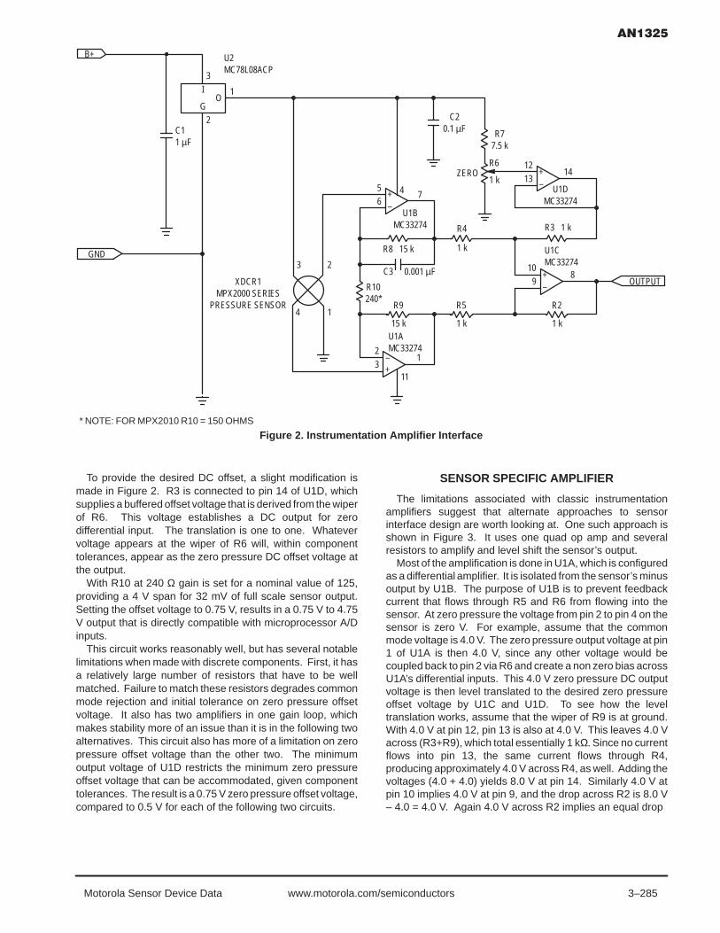
3–285Motorola Sensor Device Data www.motorola.com/semiconductors
Figure 2. Instrumentation Amplifier Interface
+–
–+
XDCR1MPX2000 SERIES
PRESSURE SENSOR
–+
–+
B+
GND
OUTPUT
IO
G
C11 µF
U2MC78L08ACP
3
1
2
1
2
4
3
12
311
R9 R5 R2
1 k15 k 1 k
89
10
U1CMC33274
R3 1 kR4
1 k
U1BMC33274
R8 15 k
C3 0.001 µF
7456
C20.1 µF R7
7.5 k
ZEROR6
1 k
1213
14
U1DMC33274
* NOTE: FOR MPX2010 R10 = 150 OHMS
U1AMC33274
R10240*
To provide the desired DC offset, a slight modification ismade in Figure 2. R3 is connected to pin 14 of U1D, whichsupplies a buffered offset voltage that is derived from the wiperof R6. This voltage establishes a DC output for zerodifferential input. The translation is one to one. Whatevervoltage appears at the wiper of R6 will, within componenttolerances, appear as the zero pressure DC offset voltage atthe output.
With R10 at 240 Ω gain is set for a nominal value of 125,providing a 4 V span for 32 mV of full scale sensor output.Setting the offset voltage to 0.75 V, results in a 0.75 V to 4.75V output that is directly compatible with microprocessor A/Dinputs.
This circuit works reasonably well, but has several notablelimitations when made with discrete components. First, it hasa relatively large number of resistors that have to be wellmatched. Failure to match these resistors degrades commonmode rejection and initial tolerance on zero pressure offsetvoltage. It also has two amplifiers in one gain loop, whichmakes stability more of an issue than it is in the following twoalternatives. This circuit also has more of a limitation on zeropressure offset voltage than the other two. The minimumoutput voltage of U1D restricts the minimum zero pressureoffset voltage that can be accommodated, given componenttolerances. The result is a 0.75 V zero pressure offset voltage,compared to 0.5 V for each of the following two circuits.
SENSOR SPECIFIC AMPLIFIER
The limitations associated with classic instrumentationamplifiers suggest that alternate approaches to sensorinterface design are worth looking at. One such approach isshown in Figure 3. It uses one quad op amp and severalresistors to amplify and level shift the sensor’s output.
Most of the amplification is done in U1A, which is configuredas a differential amplifier. It is isolated from the sensor’s minusoutput by U1B. The purpose of U1B is to prevent feedbackcurrent that flows through R5 and R6 from flowing into thesensor. At zero pressure the voltage from pin 2 to pin 4 on thesensor is zero V. For example, assume that the commonmode voltage is 4.0 V. The zero pressure output voltage at pin1 of U1A is then 4.0 V, since any other voltage would becoupled back to pin 2 via R6 and create a non zero bias acrossU1A’s differential inputs. This 4.0 V zero pressure DC outputvoltage is then level translated to the desired zero pressureoffset voltage by U1C and U1D. To see how the leveltranslation works, assume that the wiper of R9 is at ground.With 4.0 V at pin 12, pin 13 is also at 4.0 V. This leaves 4.0 Vacross (R3+R9), which total essentially 1 kΩ. Since no currentflows into pin 13, the same current flows through R4,producing approximately 4.0 V across R4, as well. Adding thevoltages (4.0 + 4.0) yields 8.0 V at pin 14. Similarly 4.0 V atpin 10 implies 4.0 V at pin 9, and the drop across R2 is 8.0 V– 4.0 = 4.0 V. Again 4.0 V across R2 implies an equal drop

3–286 Motorola Sensor Device Datawww.motorola.com/semiconductors
Figure 3. Sensor Specific Amplifier
* NOTE: FOR MPX2010 R5 = 75 OHMS
C11 µF
IO
G
3
1
2
B+
GND
OUT
R9 200
ZEROCAL.
R81.5 k
XDCR1MPX2000 SERIES
PRESSURE SENSOR
1
2
4
3
–+
U1AMC33274
143
2
TP2 +8 V
C20.1 µF
R6 7.5 kR5
120*
–+
U1BMC33274
7
11
6
5
R3820
–+
U1CMC33274
810
9
R1 2 k
R2 2 k
–+
U1DMC33274
1412
13
R4 1 k
U2MC78L08ACP
across R1, and the voltage at pin 8 is 4.0 V – 4.0 V = 0 V. Inpractice, the output of U1C will not go all the way to ground,and the voltage injected by R8 at the wiper of R9 isapproximately translated into a DC offset.
Gain is approximately equal to R6/R5(R1/R2+1), whichpredicts 125 for the values shown in Figure 3. A more exactcalculation can be performed by doing a nodal analysis, whichyields 127. Cascading the gains of U1A and U1C usingstandard op amp gain equations does not give an exact result,because the sensor’s negative going differential signal at pin4 subtracts from the DC level that is amplified by U1C. Settingoffset to 0.5 V results in an analog zero to full scale range of0.5 to 4.5 V. For this DC output voltage to be independent ofthe sensor’s common mode voltage it is necessary to satisfythe condition that R1/R2 = (R3+R9)/R4.
This approach to interface amplifier design is animprovement over the classic instrument amplifier in that ituses fewer resistors, is inherently more stable, and providesa zero pressure output voltage that can be targeted at .5 V. Ithas the same tolerance problem from matching discreteresistors that is associated with classic instrument amplifiers.
SENSOR MINI AMP
Further improvements can be made with the circuit that isshown in Figure 4. It uses one dual op amp and severalresistors to amplify and level shift the sensor’s output. To seehow this amplifier works, let’s simplify it by grounding theoutput of voltage divider R3, R5 and assuming that the dividerimpedance is added to R6, such that R6 = 12.4 k. If thecommon mode voltage at pins 2 and 4 of the sensor is 4.0 V,
then pin 2 of U2A and pin 6 of U2B are also at 4.0 V. This puts4.0 V across R6, producing 323 µA. Assuming that the currentin R4 is equal to the current in R6, 323 µA • 100 Ω producesa 32 mV drop across R4 which adds to the 4.0 V at pin 2. Theoutput voltage at pin 1 of U2A is, therefore, 4.032 V. This puts4.032 – 4.0 V across R2, producing 43 µA. The same currentflowing through R1 again produces a voltage drop of 4.0 V,which sets the output at zero. Substituting a divider outputgreater than zero into this calculation reveals that the zeropressure output voltage is equal to the output voltage ofdivider R3, R5. For this DC output voltage to be independentof the sensor’s common mode voltage it is necessary to satisfythe condition that R1/R2 = R6/R4, where R6 includes thedivider impedance.
Gain can be determined by assuming a differential output atthe sensor and going through the same calculation. To do thisassume 100 mV of differential output, which puts pin 2 of U2Aat 3.95 V, and pin 6 of U2B at 4.05 V. Therefore, 3.95 V isapplied to R6, generating 319 uA. This current flowing throughR4 produces 31.9 mV, placing pin 1 of U2A at 3950 mV + 31.9mV = 3982 mV. The voltage across R2 is then 4050 mV –3982 mV = 68 mV, which produces a current of 91 µA thatflows into R1. The output voltage is then 4.05 V + (91 µA •93.1 k) = 12.5 V. Dividing 12.5 V by the 100 mV input yieldsa gain of 125, which provides a 4 V span for 32 mV of fullscale sensor output. Setting divider R3, R5 at 0.5 V resultsin a 0.5 V to 4.5 V output that is comparable to the other twocircuits.
This circuit performs the same function as the other two withsignificantly fewer components and lower cost. In most casesit is the optimum choice for a low cost interface amplifier.

3–287Motorola Sensor Device Data www.motorola.com/semiconductors
NOTES:R7 IS NOMINALLY 39.2 k AND SELECTED FOR ZERO PRESSURE VOUT = 0.5 VFOR MPX2010 SENSORS R1 = 150 k AND R4 = 61.9 OHMS
C10.2 µF
IO
G
3
1
2
B+
GND
OUTC20.2 µF
XDCR1MPX2000 SERIES
SENSOR1
2
4
3
U1BMC33272
1
4
3
2
–+ 8
6
R1 93.1 k 1%
U1MC78L08ACP
C2 0.001 µF
R27501%
R41001%
R611 k1%
R51.33 k1%
R7TRIM
R339.2 k1%
57
U2BMC33272
Figure 4. Sensor Mini Amp
–+
PERFORMANCE
Performance differences between the three topologies areminor. Accuracy is much more dependent upon the quality ofthe resistors and amplifiers that are used and less dependenton which of the three circuits are chosen. For example, inputoffset voltage error is essentially the same for all three circuits.To a first order approximation, it is equal to total gain times thedifference in offset between the two amplifiers that are directlytied to the sensor. Errors due to resistor tolerances aresomewhat dependent upon circuit topology. However, they
are much more dependent upon the choice of resistors.Choosing 1% resistors rather than 5% resistors has a muchlarger impact on performance than the minor differences thatresult from circuit topology. Assuming a zero pressure offsetadjustment, any of these circuits with an MPX2000 seriessensor, 1% resistors and an MC33274 amplifier results in a± 5% pressure to voltage translation from 0 to 50° C. Softwarecalibration can significantly improve these numbers andeliminate the need for analog trim.
CONCLUSION
Although the classic instrumentation amplifier is the bestknown and most frequently used sensor interface amplifier, itis generally not the optimal choice for inexpensive circuitsmade from discrete components. The circuit that is shown in
Figure 4 performs the same interface function withsignificantly fewer components, less board space and at alower cost. It is generally the preferred interface topology forMPX2000 series semiconductor pressure sensors.

3–288 Motorola Sensor Device Datawww.motorola.com/semiconductors
Prepared by: Chris Winkler and Jeff BaumDiscrete Applications Engineering
ABSTRACT
The most recent advances in silicon micromachiningtechnology have given rise to a variety of low–cost pressuresensor applications and solutions. Certain applications hadpreviously been hindered by the high–cost, large size, andoverall reliability limitations of electromechanical pressuresensing devices. Furthermore, the integration of on–chiptemperature compensation and calibration has allowed asignificant improvement in the accuracy and temperaturestability of the sensor output signal. This technology allows for
the development of both analog and microcomputer–basedsystems that can accurately resolve the small pressurechanges encountered in many applications. One particularapplication of interest is the combination of a silicon pressuresensor and a microcontroller interface in the design of a digitalbarometer. The focus of the following documentation is topresent a low–cost, simple approach to designing a digitalbarometer system.
Figure 1. Barometer System
DIGIT1 DIGIT2 DIGIT3 DIGIT4
MCU
SIGNAL CONDITIONING
PRESSURESENSOR
SEMICONDUCTOR APPLICATION NOTE
REV 1

3–289Motorola Sensor Device Data www.motorola.com/semiconductors
INTRODUCTION
Figure 1 shows the overall system architecture chosen forthis application. This system serves as a building block, fromwhich more advanced systems can be developed. Enhancedaccuracy, resolution, and additional features can beintegrated in a more complex design.
There are some preliminary concerns regarding themeasurement of barometric pressure which directly affect thedesign considerations for this system. Barometric pressurerefers to the air pressure existing at any point within the earth’satmosphere. This pressure can be measured as an absolutepressure, (with reference to absolute vacuum) or can bereferenced to some other value or scale. The meteorology andavionics industries traditionally measure the absolutepressure, and then reference it to a sea level pressure value.This complicated process is used in generating maps ofweather systems. The atmospheric pressure at any altitudevaries due to changing weather conditions over time.Therefore, it can be difficult to determine the significance of aparticular pressure measurement without additionalinformation. However, once the pressure at a particularlocation and elevation is determined, the pressure can becalculated at any other altitude. Mathematically, atmosphericpressure is exponentially related to altitude. This particularsystem is designed to track variations in barometric pressureonce it is calibrated to a known pressure reference at a givenaltitude.
For simplification, the standard atmospheric pressure atsea level is assumed to be 29.9 in–Hg. “Standard” barometricpressure is measured at particular altitude at the averageweather conditions for that altitude over time. The systemdescribed in this text is specified to accurately measurebarometric pressure variations up to altitudes of 15,000 ft. Thisaltitude corresponds to a standard pressure of approximately15.0 in–Hg. As a result of changing weather conditions, thestandard pressure at a given altitude can fluctuateapproximately ±1 in–Hg. in either direction. Table 1 indicatesstandard barometric pressures at several altitudes of interest.
MC68HC11E9MICRO–
CONTROLLER
4–DIGIT LCD& MC145453
DISPLAY DRIVER
SIGNAL COND.
AMPLIFIER
MPX2100APPRESSURE
SENSOR
DATACLOCK SYNCH
Figure 2. Barometer System Block Diagram
Table 1. Altitude versus Pressure Data
Altitude (Ft.) Pressure (in–Hg)
0 29.92
500 29.38
1,000 28.85
6,000 23.97
10,000 20.57
15,000 16.86
SYSTEM OVERVIEW
In order to measure and display the correct barometricpressure, this system must perform several tasks. Themeasurement strategy is outlined below in Figure 2. First,pressure is applied to the sensor. This produces a proportionaldifferential output voltage in the millivolt range. This signalmust then be amplified and level–shifted to a single–ended,microcontroller (MCU) compatible level (0.5 – 4.5 V) by asignal conditioning circuit. The MCU will then sample thevoltage at the analog–to–digital converter (A/D) channel input,convert the digital measurement value to inches of mercury,and then display the correct pressure via the LCD interface.This process is repeated continuously.
There are several significant performance featuresimplemented into this system design. First, the system willdigitally display barometric pressure in inches of mercury, witha resolution of approximately one–tenth of an inch of mercury.In order to allow for operation over a wide altitude range (0 –15,000 ft.), the system is designed to display barometricpressures ranging from 30.5 in–Hg. to a minimum of 15.0in–Hg. The display will read “lo” if the pressure measured isbelow 30.5 in–Hg. These pressures allow for the system tooperate with the desired resolution in the range from sea–levelto approximately 15,000 ft. An overview of these features isshown in Table 2.
Table 2. System Features Overview
Display Units in–Hg
Resolution 0.1 in–Hg.
System Range 15.0 – 30.5 in–Hg.
Altitude Range 0 – 15,000 ft.
DESIGN OVERVIEW
The following sections are included to detail the systemdesign. The overall system will be described by consideringthe subsystems depicted in the system block diagram, Figure2. The design of each subsystem and its function in the overallsystem will be presented.

3–290 Motorola Sensor Device Datawww.motorola.com/semiconductors
Table 3. MPX2100AP Electrical Characteristics
Characteristic Symbol Minimum Typical Max Unit
Pressure Range POP 0 100 kPa
Supply Voltage VS 10 16 Vdc
Full Scale Span VFSS 38.5 40 41.5 mV
Zero Pressure Offset Voff ±1.0 mV
Sensitivity S 0.4 mv/kPa
Linearity 0.05 %FSS
Temperature Effect on Span 0.5 %FSS
Temperature Effect on Offset 0.2 %FSS
Pressure SensorThe first and most important subsystem is the pressure
transducer. This device converts the applied pressure into aproportional, differential voltage signal. This output signal willvary linearly with pressure. Since the applied pressure in thisapplication will approach a maximum level of 30.5 in–Hg. (100kPa) at sea level, the sensor output must have a linear outputresponse over this pressure range. Also, the applied pressuremust be measured with respect to a known reference pressure,preferably absolute zero pressure (vacuum). The device shouldalso produce a stable output over the entire operatingtemperature range.
The desired sensor for this application is a temperaturecompensated and calibrated, semiconductor pressuretransducer, such as the Motorola MPXM2102A series sensorfamily. The MPX2000 series sensors are available infull–scale pressure ranges from 10 kPa (1.5 psi) to 200 kPa(30 psi). Furthermore, they are available in a variety ofpressure configurations (gauge, differential, and absolute)and porting options. Because of the pressure ranges involvedwith barometric pressure measurement, this system willemploy an MPXM2102AS (absolute with single port). Thisdevice will produce a linear voltage output in the pressurerange of 0 to 100 kPa. The ambient pressure applied to thesingle port will be measured with respect to an evacuatedcavity (vacuum reference). The electrical characteristics forthis device are summarized in Table 3.
As indicated in Table 3, the sensor can be operated atdifferent supply voltages. The full–scale output of the sensor,which is specified at 40 mV nominally for a supply voltage of10 Vdc, changes linearly with supply voltage. All non–digitalcircuitry is operated at a regulated supply voltage of 8 Vdc.Therefore, the full–scale sensor output (also the output of thesensor at sea level) will be approximately 32 mV.
810 40 mV
The sensor output voltage at the systems minimum range(15 in–Hg.) is approximately 16.2 mV. Thus, the sensor outputover the intended range of operations is expected to vary from32 to 16.2 mV. These values can vary slightly for each sensoras the offset voltage and full–scale span tolerances indicate.
Signal Conditioning CircuitryIn order to convert the small–signal differential output signal
of the sensor to MCU compatible levels, the next subsystemincludes signal conditioning circuitry. The operationalamplifier circuit is designed to amplify, level–shift, and groundreference the output signal. The signal is converted to asingle–ended, 0.5 – 4.5 Vdc range. The schematic for thisamplifier is shown in Figure 3.
This particular circuit is based on classic instrumentationamplifier design criteria. The differential output signal of thesensor is inverted, amplified, and then level–shifted by anadjustable offset voltage (through Roffset1). The offset voltageis adjusted to produce 0.5 volts at the maximum barometricpressure (30.5 in–Hg.). The output voltage will increase fordecreasing pressure. If the output exceeds 5.1 V, a zenerprotection diode will clamp the output. This feature is includedto protect the A/D channel input of the MCU. Using the transferfunction for this circuit, the offset voltage and gain can bedetermined to provide 0.1 in–Hg of system resolution and thedesired output voltage level. The calculation of theseparameters is illustrated below.
In determining the amplifier gain and range of the trimmableoffset voltage, it is necessary to calculate the number of stepsused in the A/D conversion process to resolve 0.1 in–Hg.
(30.5 15.0)in-Hg * 10stepsHg
155 steps
The span voltage can now be determined. The resolutionprovided by an 8–bit A/D converter with low and high voltagereferences of zero and five volts, respectively, will detect 19.5mV of change per step.
VRH 5 V, VRL 0 V
Sensor Output at 30.5 in–Hg = 32.44 mVSensor Output at 15.0 in–Hg = 16.26 mV∆Sensor Output = ∆SO = 16.18 mV
Gain 3.04 VSO
187
Note: 30.5 in–Hg and 15.0 in–Hg are the assumedmaximum and minimum absolute pressures, respectively.
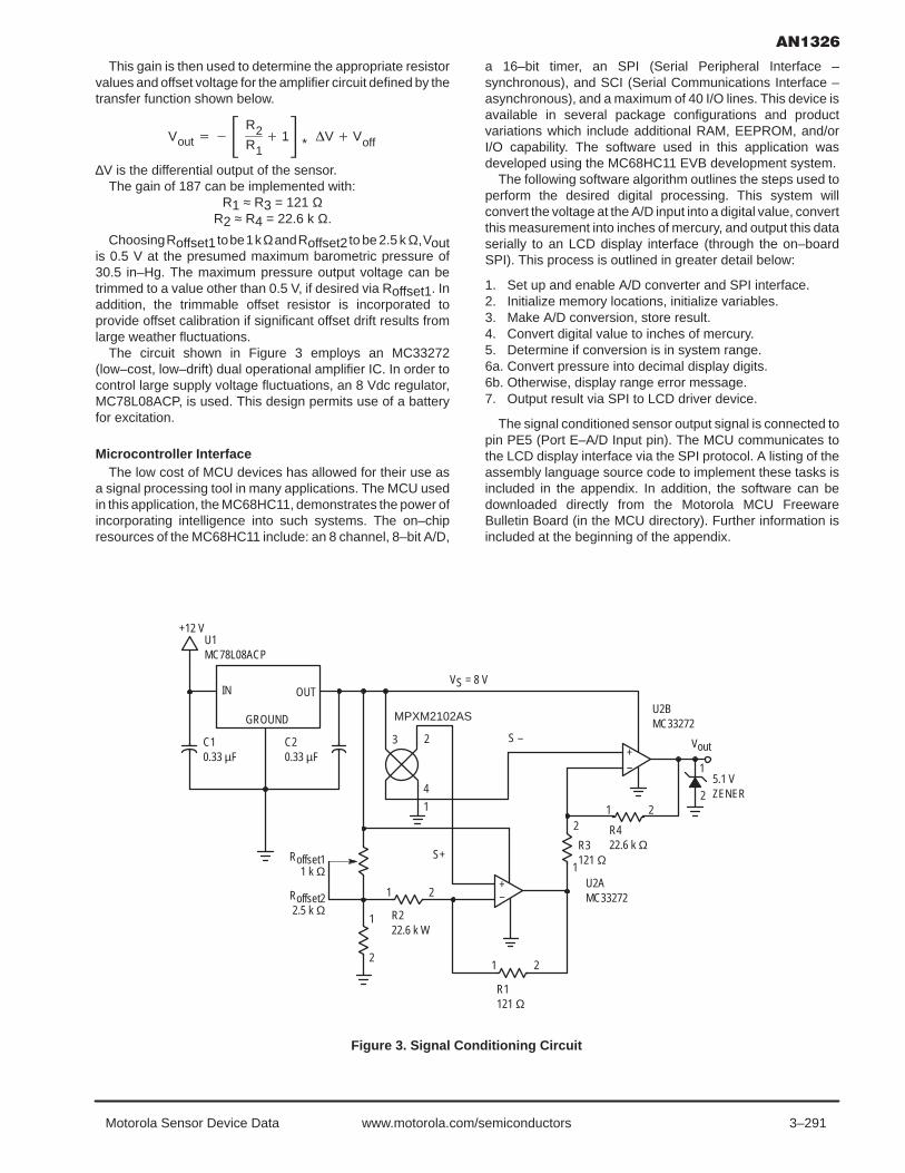
3–291Motorola Sensor Device Data www.motorola.com/semiconductors
This gain is then used to determine the appropriate resistorvalues and offset voltage for the amplifier circuit defined by thetransfer function shown below.
Vout R2R1
1 * V Voff
∆V is the differential output of the sensor.The gain of 187 can be implemented with:
R1 ≈ R3 = 121 ΩR2 ≈ R4 = 22.6 k Ω.
Choosing Roffset1 to be 1 k Ω and Roffset2 to be 2.5 k Ω, Voutis 0.5 V at the presumed maximum barometric pressure of30.5 in–Hg. The maximum pressure output voltage can betrimmed to a value other than 0.5 V, if desired via Roffset1. Inaddition, the trimmable offset resistor is incorporated toprovide offset calibration if significant offset drift results fromlarge weather fluctuations.
The circuit shown in Figure 3 employs an MC33272(low–cost, low–drift) dual operational amplifier IC. In order tocontrol large supply voltage fluctuations, an 8 Vdc regulator,MC78L08ACP, is used. This design permits use of a batteryfor excitation.
Microcontroller InterfaceThe low cost of MCU devices has allowed for their use as
a signal processing tool in many applications. The MCU usedin this application, the MC68HC11, demonstrates the power ofincorporating intelligence into such systems. The on–chipresources of the MC68HC11 include: an 8 channel, 8–bit A/D,
a 16–bit timer, an SPI (Serial Peripheral Interface –synchronous), and SCI (Serial Communications Interface –asynchronous), and a maximum of 40 I/O lines. This device isavailable in several package configurations and productvariations which include additional RAM, EEPROM, and/orI/O capability. The software used in this application wasdeveloped using the MC68HC11 EVB development system.
The following software algorithm outlines the steps used toperform the desired digital processing. This system willconvert the voltage at the A/D input into a digital value, convertthis measurement into inches of mercury, and output this dataserially to an LCD display interface (through the on–boardSPI). This process is outlined in greater detail below:
1. Set up and enable A/D converter and SPI interface.2. Initialize memory locations, initialize variables.3. Make A/D conversion, store result.4. Convert digital value to inches of mercury.5. Determine if conversion is in system range.6a. Convert pressure into decimal display digits.6b. Otherwise, display range error message.7. Output result via SPI to LCD driver device.
The signal conditioned sensor output signal is connected topin PE5 (Port E–A/D Input pin). The MCU communicates tothe LCD display interface via the SPI protocol. A listing of theassembly language source code to implement these tasks isincluded in the appendix. In addition, the software can bedownloaded directly from the Motorola MCU FreewareBulletin Board (in the MCU directory). Further information isincluded at the beginning of the appendix.
IN
GROUND
OUT
–+
3
1
4
–+
+12 VU1MC78L08ACP
VS = 8 V
U2BMC33272
Vout
5.1 VZENER
R422.6 k Ω
C10.33 µF
C20.33 µF
MPXM2102AS
Roffset11 k Ω
Roffset2 2.5 k Ω R2
22.6 k W
R1121 Ω
U2AMC33272
R3121 Ω
S –
S+
1
2
2
1 2
1 2
1
2
Figure 3. Signal Conditioning Circuit
1
2
1
2

3–292 Motorola Sensor Device Datawww.motorola.com/semiconductors
LCD InterfaceIn order to digitally display the barometric pressure
conversion, a serial LCD interface was developed tocommunicate with the MCU. This system includes anMC145453 CMOS serial interface/LCD driver, and a 4–digit,non–multiplexed LCD. In order for the MCU to communicatecorrectly with the interface, it must serially transmit six bytesfor each conversion. This includes a start byte, a byte for each
of the four decimal display digits, and a stop byte. Forformatting purposes, decimal points and blank digits can bedisplayed through appropriate bit patterns. The control ofdisplay digits and data transmission is executed in the sourcecode through subroutines BCDCONV, LOOKUP, SP12LCD,and TRANSFER. A block diagram of this interface is includedbelow.
CONCLUSION
This digital barometer system described herein is anexcellent example of a sensing system using solid statecomponents and software to accurately measure barometricpressure. This system serves as a foundation from whichmore complex systems can be developed. The MPXM2102A
series pressure sensors provide the calibration andtemperature compensation necessary to achieve the desiredaccuracy and interface simplicity for barometric pressuresensing applications.
MC68HC11
MOSI
SCK
DIGIT1 DIGIT2 DIGIT3 DIGIT4
BP BP
VDDBP IN BP OUT
OSC IN
OUT 33
DATA
CLOCK
VSSOUT1
MC145453
+5 V
20
1
Figure 4. LCD Display Interface Diagram

3–293Motorola Sensor Device Data www.motorola.com/semiconductors
APPENDIX
MC68HC11 Barometer Software Available on:
Motorola Electronic Bulletin BoardMCU Freeware Line8–bit, no parity, 1 stop bit1200/300 baud(512) 891–FREE (3733)
* BAROMETER APPLICATIONS PROJECT – Chris Winkler* Developed: October 1st, 1992 – Motorola Discrete Applications* This code will be used to implement an MC68HC11 Micro–Controller* as a processing unit for a simple barometer system.* The HC11 will interface with an MPX2100AP to monitor,store* and display measured Barometric pressure via the 8–bit A/D channel* The sensor output (32mv max) will be amplified to .5 – 2.5 V dc* The processor will interface with a 4–digit LCD (FE202) via* a Motorola LCD driver (MC145453) to display the pressure* within +/– one tenth of an inch of mercury.* The systems range is 15.0 – 30.5 in–Hg
* A/D & CPU Register Assignment* This code will use index addressing to access the* important control registers. All addressing will be* indexed off of REGBASE, the base address for these registers.
REGBASE EQU $1000 * register base of control registerADCTL EQU $30 * offset of A/D control registerADR2 EQU $32 * offset of A/D results registerADOPT EQU $39 * offset for A/D option register locationPORTB EQU $04 * Location of PORTB used for conversionPORTD EQU $08 * PORTD Data Register IndexDDRD EQU $09 * offset of Data Direction Reg.SPCR EQU $28 * offset of SPI Control Reg.SPSR EQU $29 * offset of SPI Status Reg.SPDR EQU $2A * offset of SPI Data Reg.
* User Variables* The following locations are used to store important measurements* and calculations used in determining the altitude. They* are located in the lower 256 bytes of user RAM
DIGIT1 EQU $0001 * BCD blank digit (not used)DIGIT2 EQU $0002 * BCD tens digit for pressureDIGIT3 EQU $0003 * BCD tenths digit for pressureDIGIT4 EQU $0004 * BCD ones digit for pressureCOUNTER EQU $0005 * Variable to send 5 dummy bytesPOFFSET EQU $0010 * Storage Location for max pressure offsetSENSOUT EQU $0012 * Storage location for previous conversionRESULT EQU $0014 * Storage of Pressure(in Hg) in hex formatFLAG EQU $0016 * Determines if measurement is within range
* MAIN PROGRAM* The conversion process involves the following steps:** 1. Set–Up SPI device– SPI_CNFG* 2. Set–Up A/D, Constants SET_UP* 3. Read A/D, store sample ADCONV* 4. Convert into in–Hg IN_HG* 5. Determine FLAG condition IN_HG* a. Display error ERROR* b. Continue Conversion INRANGE* 6. Convert hex to BCD format BCDCONV* 7. Convert LCD display digits LOOKUP* 8. Output via SPI to LCD SPI2LCD
* This process is continually repeated as the loop CONVERT* runs unconditionally through BRA (the BRANCH ALWAYS statement)* Repeats to step 3 indefinitely.

3–294 Motorola Sensor Device Datawww.motorola.com/semiconductors
ORG $C000 * DESIGNATES START OF MEMORY MAP FOR USER CODELDX #REGBASE * Location of base register for indirect adrBSR SPI_CNFG * Set–up SPI Module for data X–mit to LCDBSR SET_UP * Power–Up A/D, initialize constants
CONVERT BSR ADCONV * Calls subroutine to make an A/D conversionBSR DELAY * Delay routine to prevent LCD flickeringBSR IN_HG * Converts hex format to in of Hg
* The value of FLAG passed from IN_HG is used to determine* If a range error has occurred. The following logical* statements are used to either allow further conversion or jump* to a routine to display a range error message.
LDAB FLAG * Determines if an range Error has ocurredCMPB #$80 * If No Error detected (FLAG=$80) thenBEQ INRANGE * system will continue conversion processBSR ERROR * If error occurs (FLAG<>80), branch to ERRORBRA OUTPUT * Branches to output ERROR code to display
* No Error Detected, Conversion Process Continues
INRANGE JSR BCDCONV * Converts Hex Result to BCDJSR LOOKUP * Uses Look–Up Table for BCD–Decimal
OUTPUT JSR SPI2LCD * Output transmission to LCDBRA CONVERT * Continually converts using Branch Always
* Subroutine SPI_CNFG* Purpose is to initialize SPI for transmission* and clear the display before conversion.
SPI_CNFG BSET PORTD,X #$20 * Set SPI SS Line High to prevent glitchLDAA #$38 * Initializing Data Direction for Port DSTAA DDRD,X * Selecting SS, MOSI, SCK as outputs only
LDAA #$5D * Initialize SPI–Control RegisterSTAA SPCR,X * selecting SPE,MSTR,CPOL,CPHA,CPRO
LDAA #$5 * sets counter to X–mit 5 blank bytesSTAA COUNTERLDAA SPSR,X * Must read SPSR to clear SPIF Flag
CLRA * Transmission of Blank Bytes to LCD
ERASELCD JSR TRANSFER * Calls subroutine to transmitDEC COUNTERBNE ERASELCD
RTS
* Subroutine SET_UP* Purpose is to initialize constants and to power–up A/D* and to initialize POFFSET used in conversion purposes.SET_UP LDAA #$90 * selects ADPU bit in OPTION register
STAA ADOPT,X * Power–Up of A/D completeLDD #$0131+$001A * Initialize POFFSETSTD POFFSET * POFFSET = 305 – 25 in hexLDAA #$00 * or Pmax + offset voltage (5 V)RTS
* Subroutine DELAY* Purpose is to delay the conversion process* to minimize LCD flickering.
DELAY LDA #$FF * Loop for delay of displayOUTLOOP LDB #$FF * Delay = clk/255*255INLOOP DECB
BNE INLOOPDECABNE OUTLOOPRTS
* Subroutine ADCONV* Purpose is to read the A/D input, store the conversion into* SENSOUT. For conversion purposes later.
ADCONV LDX #REGBASE * loads base register for indirect addressingLDAA #$25STAA ADCTL,X * initializes A/D cont. register SCAN=1,MULT=0

3–295Motorola Sensor Device Data www.motorola.com/semiconductors
WTCONV BRCLR ADCTL,X #$80 WTCONV * Wait for completion of conversion flagLDAB ADR2,X * Loads conversion result into AccumulatorCLRASTD SENSOUT * Stores conversion as SENSOUTRTS
* Subroutine IN_HG* Purpose is to convert the measured pressure SENSOUT, into* units of in–Hg, represented by a hex value of 305–150* This represents the range 30.5 – 15.0 in–HgIN_HG LDD POFFSET * Loads maximum offset for subtraction
SUBD SENSOUT * RESULT = POFFSET–SENSOUT in hex formatSTD RESULT * Stores hex result for P, in HgCMPD #305BHI TOHIGH
CMPD #150BLO TOLOW
LDAB #$80STAB FLAGBRA END_CONV
TOHIGH LDAB #$FFSTAB FLAGBRA END_CONV
TOLOW LDAB #$00STAB FLAG
END_CONV RTS
* Subroutine ERROR* This subroutine sets the display digits to output* an error message having detected an out of range* measurement in the main program from FLAG
ERROR LDAB #$00 * Initialize digits 1,4 to blanksSTAB DIGIT1STAB DIGIT4
LDAB FLAG * FLAG is used to determineCMPB #$00 * if above or below range.BNE SET_HI * If above range GOTO SET_HI
LDAB #$0E * ELSE display LO on displaySTAB DIGIT2 * Set DIGIT2=L,DIGIT3=OLDAB #$7ESTAB DIGIT3BRA END_ERR * GOTO exit of subroutine
SET_HI LDAB #$37 * Set DIGIT2=H,DIGIT3=1STAB DIGIT2LDAB #$30STAB DIGIT3
END_ERR RTS
* Subroutine BCDCONV* Purpose is to convert ALTITUDE from hex to BCD* uses standard HEX–BCD conversion scheme* Divide HEX/10 store Remainder, swap Q & R, repeat* process until remainder = 0.
BCDCONV LDAA #$00 * Default Digits 2,3,4 to 0STAA DIGIT2STAA DIGIT3STAA DIGIT4LDY #DIGIT4 * Conversion starts with lowest digitLDD RESULT * Load voltage to be converted
CONVLP LDX #$A * Divide hex digit by 10IDIV * Quotient in X, Remainder in DSTAB 0,Y * stores 8 LSB’s of remainder as BCD digitDEYCPX #$0 * Determines if last digit storedXGDX * Exchanges remainder & quotientBNE CONVLPLDX #REGBASE * Reloads BASE into main programRTS
* Subroutine LOOKUP

3–296 Motorola Sensor Device Datawww.motorola.com/semiconductors
* Purpose is to implement a Look–Up conversion* The BCD is used to index off of TABLE* where the appropriate hex code to display* that decimal digit is contained.* DIGIT4,3,2 are converted only.
LOOKUP LDX #DIGIT1+4 * Counter starts at 5TABLOOP DEX * Start with Digit4
LDY #TABLE * Loads table base into Y–pointerLDAB 0,X * Loads current digit into BABY * Adds to base to index off TABLELDAA 0,Y * Stores HEX segment result in ASTAA 0,XCPX #DIGIT2 * Loop condition complete, DIGIT2 ConvertedBNE TABLOOP
RTS
* Subroutine SPI2LCD* Purpose is to output digits to LCD via SPI* The format for this is to send a start byte,* four digits, and a stop byte. This system* will have 3 significant digits: blank digit* and three decimal digits.
* Sending LCD Start Byte
SPI2LCD LDX #REGBASELDAA SPSR,X * Reads to clear SPIF flagLDAA #$02 * Byte, no colon, start bitBSR TRANSFER * Transmit byte
* Initializing decimal point & blank digitLDAA DIGIT3 * Sets MSB for decimal pt.ORA #$80 * after digit 3STAA DIGIT3
LDAA #$00 * Set 1st digit as blankSTAA DIGIT1
* Sending four decimal digits
LDY #DIGIT1 * Pointer set to send 4 bytesDLOOP LDAA 0,Y * Loads digit to be x–mitted
BSR TRANSFER * Transmit byteINY * Branch until both bytes sentCPY #DIGIT4+1BNE DLOOP
* Sending LCD Stop Byte
LDAA #$00 * end byte requires all 0’sBSR TRANSFER * Transmit byte
RTS
* Subroutine TRANSFER* Purpose is to send data bits to SPI* and wait for conversion complete flag bit to be set.
TRANSFER LDX #REGBASEBCLR PORTD,X #$20 * Assert SS Line to start X–misssionSTAA SPDR,X * Load Data into Data Reg.,X–mit
XMIT BRCLR SPSR,X #$80 XMIT* Wait for flagBSET PORTD,X #$20 * DISASSERT SS LineLDAB SPSR,X * Read to Clear SPI Flag
RTS
* Location for FCB memory for look–up table* There are 11 possible digits: blank, 0–9
TABLE FCB $7E,$30,$6D,$79,$33,$5B,$5F,$70,$7F,$73,$00END

3–297Motorola Sensor Device Data www.motorola.com/semiconductors
"! " " ! ! "
Prepared by: Brian PickardSensor Products DivisionSemiconductor Products Sector
INTRODUCTION
Motorola offers a wide variety of ported, pressure sensingdevices which incorporate a hose barb and mounting tabs.They were designed to give the widest range of designflexibility. The hose barbs are 1/8″ (≈3 mm) diameter and thetabs have #6 mounting holes. These sizes are very commonand should make installation relatively simple. Moreimportantly, and often overlooked, are the techniques used inmounting and adapting the ported pressure sensors. Thisapplication note provides some recommendations on types offasteners for mounting, how to use them with Motorolasensors, and identifies some suppliers. This document alsorecommends a variety of hoses, hose clamps, and theirrespective suppliers.
This information applies to all Motorola MPX pressuresensors with ported packages, which includes the packagesshown in Figure 1.
Single Side Port Differential Port
Axial Port Stovepipe Port
Figure 1. MPX Pressure Sensors withPorted Packages
A review of recommended mounting hardware, mountingtorque, hose applications, and hose clamps is also providedfor reference.
MOUNTING HARDWARE
Mounting hardware is an integral part of package design.Different applications will call for different types of hardware.When choosing mounting hardware, there are three importantfactors:
• permanent versus removable
• application
• cost
The purpose of mounting hardware is not only to secure thesensor in place, but also to remove the stresses from thesensor leads. In addition, these stresses can be high if thehose is not properly secured to the sensor port. Screws, rivets,push–pins, and clips are a few types of hardware that can beused. Refer to Figure 2.
Push–PinRivetScrew
Figure 2. Mounting Hardware
SEMICONDUCTOR APPLICATION NOTE
REV 1

3–298 Motorola Sensor Device Datawww.motorola.com/semiconductors
Figure 3. Case Outline DrawingsTop: Case 371D–03, Issue C
Bottom: Case 350–05, Issue J
NOTES:1. DIMENSIONING AND TOLERANCING PER
ANSI Y14.5M, 1982.2. CONTROLLING DIMENSION: INCH.
DIM MIN MAX MIN MAXMILLIMETERSINCHES
A 1.080 1.120 27.43 28.45B 0.740 0.760 18.80 19.30C 0.630 0.650 16.00 16.51D 0.016 0.020 0.41 0.51E 0.160 0.180 4.06 4.57F 0.048 0.064 1.22 1.63G 0.100 BSC 2.54 BSCJ 0.014 0.016 0.36 0.41KN 0.070 0.080 1.78 2.03P 0.150 0.160 3.81 4.06Q 0.150 0.160 3.81 4.06R 0.440 0.460 11.18 11.68S 0.695 0.725 17.65 18.42U 0.840 0.860 21.34 21.84V 0.182 0.194 4.62 4.92
E
C
J
V
–T–
PORT #2VACUUM
PIN 1
4 PLD
–P–
G
K
MQM0.25 (0.010) T
U
A
F
S
N B
SPM0.13 (0.005) Q ST
–Q–
R
1 2 3 4
POSITIVEPRESSURE
0.220 0.240 5.59 6.10
SEATINGPLANE
B
N
R
C
J
–T–
D
F
U
HL
PORT #1POSITIVE
PRESSURE
PIN 1
–A–
–Q–
S
K
G4 PL
–P–SQM0.25 (0.010) T
SSM0.13 (0.005) Q ST
1 2 3 4
NOTES:1. DIMENSIONING AND TOLERANCING PER ANSI
Y14.5, 1982.2. CONTROLLING DIMENSION: INCH.
DIM MIN MAX MIN MAXMILLIMETERSINCHES
A 1.145 1.175 29.08 29.85B 0.685 0.715 17.40 18.16C 0.305 0.325 7.75 8.26D 0.016 0.020 0.41 0.51F 0.048 0.064 1.22 1.63G 0.100 BSC 2.54 BSCH 0.182 0.194 4.62 4.93J 0.014 0.016 0.36 0.41K 0.695 0.725 17.65 18.42L 0.290 0.300 7.37 7.62N 0.420 0.440 10.67 11.18P 0.153 0.159 3.89 4.04Q 0.153 0.159 3.89 4.04R 0.230 0.250 5.84 6.35SU 0.910 BSC 23.11 BSC
0.220 0.240 5.59 6.10
To mount any of the devices except Case 371–07/08 and867E) to a flat surface such as a circuit board, the spacing anddiameter for the mounting holes should be made according toFigure 3.
Mounting ScrewsMounting screws are recommended for making a very
secure, yet removable connection. The screws can be eithermetal or nylon, depending on the application. The holes are0.155″ diameter which fits a #6 machine screw. The screw canbe threaded directly into the base mounting surface or gothrough the base and use a flat washer and nut (on a circuitboard) to secure to the device.
MOUNTING TORQUE
The torque specifications are very important. The sensorpackage should not be over tightened because it can crack,causing the sensor to leak. The recommended torquespecification for the sensor packages are as follows:
Port Style Torque Range
Single side port: port side down
port side upDifferential port (dual port)
Axial side port
3–4 in– lb6–7 in– lb9–10 in– lb9–10 in– lb
The torque range is based on installation at roomtemperature. Since the sensor thermoplastic material has ahigher TCE (temperature coefficient of expansion) thancommon metals, the torque will increase as temperatureincreases. Therefore, if the device will be subjected to very lowtemperatures, the torque may need to be increased slightly. Ifa precision torque wrench is not available, these torques allwork out to be roughly 1/2 of a turn past “finger tight” (contact)at room temperature.
Tightening beyond these recommendations may damagethe package, or affect the performance of the device.

3–299Motorola Sensor Device Data www.motorola.com/semiconductors
Nylon ScrewsMotorola recommends the use of #6–32 nylon screws as a
hardware option. However, they should not be torquedexcessively. The nylon screw will twist and deform underhigher than recommended torque. These screws should beused with a nylon nut.
RivetsRivets are excellent fasteners which are strong and very
inexpensive. However, they are a permanent connection.Plastic rivets are recommended because metal rivets maydamage the plastic package. When selecting a rivet size, themost important dimension, besides diameter, is the grip range.The grip range is the combined thickness of the sensorpackage and the thickness of the mounting surface. Packagethicknesses are listed below.
Port Style Thickness, a Grip Range = a + b
Single side portDual side portAxial side portStovepipe port
0.321″ (8.15 mm)0.420″ (10.66 mm)0.321″ (8.15 mm)(Does not apply)
a
b
Push–PinsPlastic push pins or ITW FasTex “Christmas Tree” pins are
an excellent way to make a low cost and easily removableconnection. However, these fasteners should not be used forpermanent connections. Remember, the fastener should takeall of the static and dynamic loads off the sensor leads. Thistype of fastener does not do this completely.
HOSE APPLICATIONS
By using a hose, a sensor can be located in a convenientplace away from the actual sensing location which could be ahazardous and difficult area to reach. There are many typesof hoses on the market. They have different wall thicknesses,working pressures, working temperatures, materialcompositions, and media compatibilities. All of the hosesreferenced here are 1/8″ inside diameter and 1/16″ wallthickness, which produces a 1/4″ outside diameter. Since allthe port hose barbs are 1/8″, they require 1/8″ inside diameterhose. The intent is for use in air only and any questions abouthoses for your specific application should be directed to thehose manufacturer. Four main types of hose are available:
• Vinyl • Tygon • Urethane • Nylon
Vinyl hose is inexpensive and is best in applications withpressures under 50 psig and at room temperature. It is flexibleand durable and should not crack or deteriorate with age. Thistype of hose should be used with a hose clamp such as those
listed later in this application note. Two brands of vinyl hoseare:
HoseWall
Thickness
Max. Press.@ 70°F(24°C)
Max.Temp.
(°F)/(°C)
Clippard #3814–1 Herco Clear #0500–037
1/16″1/16″
10554
100/(38)180/(82)
Tygon tubing is slightly more expensive than vinyl, but it isthe most common brand, and it is also very flexible. It also isrecommended for use at room temperature and applicationsbelow 50 psig. This tubing is also recommended forapplications where the hose may be removed and reattachedseveral times. This tubing should also be used with a hoseclamp.
TubingWall
Thickness
Max. Press.@ 73°F(25°C)
Max. Temp.(°F)/(°C)
Tygon B–44–3 1/16″ 62 165/(74)
Urethane tubing is the most expensive of the four typesdescribed herein. It can be used at higher pressures (up to 100psig) and temperatures up to 100°F (38°C). It is flexible,although its flexibility is not as good as vinyl or Tygon.Urethane tubing is very strong and it is not necessary to usea hose clamp, although it is recommended.
Two brands of urethane hose are:
HoseWall
Thickness
Max. Press.@ 70°F(24°C)
Max.Temp.
(°F)/(°C)
Clippard #3814–6Herco Clear #0585–037
1/16″1/16″
105105
120/(49)225/(107)
Nylon tubing does not work well with Motorola’s sensors. Itis typically used in high pressure applications with metalfittings (such as compressed air).
HOSE CLAMPS
Hose clamps should be employed for use with all hoseslisted above. They provide a strong connection with the sensorwhich prevents the hose from working itself off, and alsoreduces the chance of leakage. There are many types of hoseclamps that can be used with the ported sensors. Here aresome of the most common hose clamps used with hoses.

3–300 Motorola Sensor Device Datawww.motorola.com/semiconductors
Crimp–on Clamp Nylon Snap
Spring Wire Screw–on
Figure 4. Hose Clamps
The two clamps most recommended by Motorola are thecrimp–on clamp and the screw–on, Clippard reusable clamp.The crimp–on type clamp is offered from both Ryan Herco(#0929–007) and Clippard (#5000–2). Once crimped in place,it provides a very secure hold, but it is not easily removed andis not reusable. The Clippard, reusable hose clamp is a brass,self–threading clamp, which provides an equally strong grip asthe crimp–on type just described. The drawback is thereusable clamp is considerably more expensive. The nylonsnap is also reusable, however the size options do not matchthe necessary outside diameter. The spring wire clamp,common in the automotive industry, and known for its very lowcost and ease of use, also has a size matching problem.Custom fit spring wire clamps may provide some cost savingsin particular applications.
HosesNorton–Performance PlasticsWorldwide Headquarters150 Dey Road, Wayne, NJ 07470–4599 USA(201) 596–4700Telex: 710–988–5834USAP.O. Box 3660, Akron, OH 44309–3660USA(216) 798–9240FAX: (216) 798–0358
Clippard Instrument Laboratory, Inc.7390 Colerain Rd.Cincinnati, Ohio 45239, USA(513) 521–4261FAX: (513) 521–4464
Ryan Herco Products CorporationP.O. Box 588Burbank, CA 915031–800–423–2589FAX: (818) 842–4488
Spring Wire ClampsRotorClip, Inc.187 Davidson AvenueSomerset, NJ 08875–04611–800–631–5857 Ext. 255
Rivets and Push–PinsITW FasTex195 Algonquin RoadDes Plaines, IL 60016(708) 299–2222FAX: (708) 390–8727
BoltsQuality Screw and Nut Company1331 Jarvis AvenueElk Grove Village, IL 60007(312) 593–1600
Crimp–on and Nylon ClampsRyan Herco Products CorporationP.O. Box 588Burbank, CA 915031–800–423–2589FAX: (818) 842–4488
Crimp–on and Screw–on ClampsClippard Instrument Laboratory, Inc.7390 Colerain Rd.Cincinnati, Ohio 45239, USA(513) 521–4261FAX: (513) 521–4464
SUPPLIER LIST

3–301Motorola Sensor Device Data www.motorola.com/semiconductors
Prepared by: JC HamelainToulouse Pressure Sensor LaboratorySemiconductor Products Sector, Toulouse, France
INTRODUCTION
Motorola Discrete Products provides a complete solutionfor designing a low cost system for direct and accurate liquidlevel control using an ac powered pump or solenoid valve.This circuit approach which exclusively uses Motorolasemiconductor parts, incorporates a piezoresistive pressuresensor with on–chip temperature compensation and a newsolid–state relay with an integrated power triac, to drivedirectly the liquid level control equipment from the domestic110/220 V 50/60 Hz ac main power line.
PRESSURE SENSOR DESCRIPTION
The MPXM2000 Series pressure sensor integrateson–chip, laser–trimmed resistors for offset calibration andtemperature compensation. The pressure sensitive elementis a patented, single piezoresistive implant which replaces thefour resistor Wheatstone bridge traditionally used by mostpressure sensor manufacturers.
MPAK AXIAL PORTCASE 1320A
Depending on the application and pressure range, the sensormay be chosen from the following portfolio. For this applicationthe MPXM2010GS was selected.
Device Pressure Range Application Sensitivity*
MPXM2010GS 0 to 10 kPa ± 0.01 kPa (1 mm H2O)MPXM2053GS 0 to 50 kPa ± 0.05 kPa (5 mm H2O)MPXM2102GS 0 to 100 kPa ± 0.1 kPa (10 mm H2O)MPXM2202GS 0 to 200 kPa ± 0.2 kPa (20 mm H2O)* after proper gain adjustment
Pin 3
RS1
Rp X–ducer
Roff1
Pin 2
Pin 4
+ Vout
– Vout
Laser Trimmed On–Chip
RS2
Pin 1
Roff2
+ VSR1
R2
Figure 1. Pressure Sensor MPXM2000 Series
SEMICONDUCTOR APPLICATION NOTE
REV 2

3–302 Motorola Sensor Device Datawww.motorola.com/semiconductors
POWER OPTO ISOLATOR MOC2A60 DESCRIPTION
The MOC2A60 is a new Motorola POWER OPTO isolatorand consists of a gallium arsenide, infrared emitting diode,which is optically coupled to a zero–cross triac driver and apower triac. It is capable of driving a load of up to 2 A (rms)directly from a line voltage of 220 V (50/60 Hz).
ZVA*
Device Schematic
1, 4, 5, 6, 8. No Pin1, 4, 5, 6, 2. LED Cathode1, 4, 5, 6, 3. LED Anode1, 4, 5, 6, 7. Main Terminal1, 4, 5, 6, 9. Main Terminal
* Zero Voltage Activate Circuit
9
7
3
2
CASE 417PLASTIC
PACKAGE
Figure 2. MOC2A60 POWER OPTO Isolator
SIGNAL CONDITIONING
When a full range pressure is applied to the MPXM2010GS,it will provide an output of about 20 mV (at an 8 V supply).Therefore, for an application using only a few percent of thepressure range, the available signal may be as low as a fewhundred microvolts. To be useful, the sensor signal must beamplified. This is achieved via a true differential amplifier (A1and A2) as shown in Figure 4. The GAIN ADJ (500 ohm)resistor, RG, sets the gain to about 200.
The differential output of this stage is amplified by a secondstage (A3) with a variable OFFSET resistor. This stageperforms a differential to single–ended output conversion andreferences this output to the adjustable offset voltage. Thisoutput is then compared to a voltage (VREF = 4 V at TP2) atthe input of the third stage (A4).
This last amplifier is used as an inverted comparatoramplifier with hysteresis (Schmitt trigger) which provides alogic signal (TP3) within a preset range variation of about 10%of the input (selected by the ratio R9/(R9 + R7).
If the pressure sensor delivers a voltage to the input of theSchmitt trigger (pin 13) lower than the reference voltage (pin12), then the output voltage (pin 14) is high and the drivecurrent for the power stage MOC2A60 is provided. When the
sensor output increases above the reference voltage, theoutput at pin 14 goes low and no drive current is available.
The amplifier used is a Motorola MC33179. This is a quadamplifier with large current output drive capability (more than80 mA).
OUTPUT POWER STAGE
For safety reasons, it is important to prevent any directcontact between the ac main power line and the liquidenvironment or the tank. In order to maintain full isolationbetween the sensor circuitry and the main power, thesolid–state relay is placed between the low voltage circuit(sensor and amplifier) and the ac power line used by the pumpand compressor.
The output of the last stage of the MC33179 is used as acurrent source to drive the LED (light emitting diode). Theseries resistor, R8, limits the current into the LED toapproximately 15 mA and guarantees an optimum drive for thepower opto–triac. The LD1 (MFOE76), which is an infraredlight emitting diode, is used as an indicator to detect when theload is under power.
The MOC2A60 works like a switch to turn ON or OFF thepump’s power source. This device can drive up to 2 A for anac load and is perfectly suited for the medium power motors(less than 500 watts) used in many applications. It consists ofan opto–triac driving a power triac and has a zero–crossingdetection to limit the power line disturbance problems whenfast switching selfic loads. An RC network, placed in parallelwith the output of the solid–state relay is not required, but it isgood design practice for managing large voltage spikescoming from the inductive load commutation. The load itself(motor or solenoid valve) is connected in series with thesolid–state relay to the main power line.
EXAMPLE OF APPLICATION:ACCURATE LIQUID LEVEL MONITORING
The purpose of the described application is to provide anelectronic system which maintains a constant liquid level in atank (within ± 5 mm H2O). The liquid level is kept constant inthe tank by an ac electric pump and a pressure sensor whichprovides the feedback information. The tank may be of anysize. The application is not affected by the volume of the tankbut only by the difference in the liquid level. Of course, themaximum level in the tank must correspond to a pressurewithin the operating range of the pressure sensor.
LIQUID LEVEL SENSORS
Motorola has developed a piezoresistive pressure sensorfamily which is very well adapted for level sensing, especiallywhen using an air pipe sensing method. These devices mayalso be used with a bubbling method or equivalent.

3–303Motorola Sensor Device Data www.motorola.com/semiconductors
Open Pipe Before Calibration
Control Module
PressureSensor
Air
Liquid Level in the Pipe
ElectricalPump
AC Line
ReferenceLevel
H
Figure 3. Liquid Level Monitoring
LEVEL SENSING THEORY
If a pipe is placed vertically, with one end dipped into a liquidand the other end opened, the level in the pipe will be exactlythe same as the level in the tank. However, if the upper end ofthe pipe is closed off and some air volume is trapped, thepressure in the pipe will vary proportionally with the liquid levelchange in the tank.
For example, if we assume that the liquid is water and thatthe water level rises in the tank by 10 mm, then the pressurein the pipe will increase by that same value (10 mm of water).
A gauge pressure sensor has one side connected to thepipe (pressure side) and the other side open to ambient (in thiscase, atmospheric) pressure. The pressure difference which
corresponds to the change in the tank level is measured by thepressure sensor.
PRESSURE SENSOR CHOICE
In this example, a level sensing of 10 mm of water is desired.The equivalent pressure in kilo pascals is 0.09806 kPa. In thiscase, Motorola’s temperature compensated 0–10 kPa,MPXM2010GS is an excellent choice. The sensor output, witha pressure of 0.09806 kPa applied, will result in 2.0 mV/kPax 0.09806 = 0.196 mV.
The sensing system is designed with an amplifier gain ofabout 1000. Thus, the conditioned signal voltage given by themodule is 1000 x 0.196 mV = 0.196 V with 10 mm – H2Opressure.
Table 1. Liquid Level Sensors
METHOD SENSOR ADVANTAGE DISADVANTAGES
Liquid weight Magnetoresitive Low power, no active electronic Low resolution, range limited
Magnetoresitive Very high resolution Complex electronic
Ultrasonic Easy to install Need high power, low accuracy
Liquid resistivity No active electronic No active electronic Low resolution, liquid dependent
String potentiometer Potentiometer Low power, no active electronic Poor linearity, corrosion
Pressure Silicon sensors Inexpensive good resolution, widerange measurements
Active electronic, need power

3–304 Motorola Sensor Device Datawww.motorola.com/semiconductors
RG = 500 ΩR1, R2 = 100 kR5, R7 = 100 kR3, R4 . . . R6 = 10 kR9 . . . R11 = 10 kR8 = 100Roff = 25 k var
a1 . . . a4 = 1/4 MC33179D1 = MLED76MC7808ac = REGL 8 VDCTR = TRANSFORMER 220:12 VC1 = 40 µF 40 V
ÉÉÉÉ
ÉÉÉÉ
ÉÉÉÉÉÉÉÉ
ÉÉ
É
ÉÉ
ÉÉÉÉ
ÉÉÉÉ
ÉÉÉÉ
Offset Adjust Reference ADJ
Roff R10
ÉÉR11
R9R7
R3
R4R2
R1
RG
3 2
41
5
6 –+ a2
a1
2
13 +
–
4
7
11
Gain ADJ
+
+–
10
9
8
TP1
TP2
+ 12
– 13a3 a4
14
TP3
R6
R8
D1RC
Motor
N
P
L
TR 220 VAC
+8 VDCC1
MPXM2010GS
ÉÉR5
MC78L08
MOC2A60
Figure 4. Electrical Circuit
LiquidLevel
PressureSensing
(TP1)
TriggerVoltage(TP3)
PumpVoltage (AC220V)
Max
Min
7 V
0
4.3 V
0.4 V Ref (TP2)
3.7 V
Sensing for minimum level (pumping into the tank)
The sensing probe is tied to the positive pressure port of the sensor. The pump is turned on to fill the tank when the minimum level is reached.
Figure 5. Functional Diagram
10 mm

3–305Motorola Sensor Device Data www.motorola.com/semiconductors
LEVEL CONTROL MODES
This application describes two ways to keep the liquid levelconstant in the tank; first, by pumping the water out if the liquidlevel rises above the reference, or second, by pumping thewater in if the liquid level drops below the reference.
If pumping water out, the pump must be OFF when the liquidlevel is below the reference level. To turn the pump ON, thesensor signal must be decreased to drop the input to theSchmitt trigger below the reference voltage. To do this, thesensing pipe must be connected to the NEGATIVE pressureport (back or vacuum side) of the sensor. In the condition whenthe pressure increases (liquid level rises), the sensor voltagewill decrease and the pump will turn ON when the sensoroutput crosses the referenced level. As pumping continues,the level in the tank decreases (thus the pressure on thesensor decreases) and the sensor signal increases back upto the trigger point where the pump was turned OFF.
In the case of pumping water into the tank, the pump mustbe OFF when the liquid level is above the reference level. Toturn ON the pump, the sensor signal must be decreased todrive the input Schmitt trigger below the reference voltage. Todo this, the sensing pipe must be connected to the POSITIVEpressure port (top side) of the sensor. In this configurationwhen the pressure on the sensor decreases, (liquid leveldrops) the sensor voltage also decreases and the pump isturned ON when the signal exceeds the reference. Aspumping continues, the water level increases and when themaximum level is reached, the Schmitt trigger turns the pumpOFF.
ADJUSTMENTS
The sensing tube is placed into the water at a distancebelow the minimum limit level anywhere in the tank. The other
end of the tube is opened to atmosphere. When the tank isfilled to the desired maximum (or minimum) level, the pressuresensor is connected to the tube with the desired portconfiguration for the application. Then the water level in thetank is the reference.
After connecting the tube to the pressure sensor, themodule must be adjusted to control the water level. The outputvoltage at TP1 is preadjusted to about 4 V (half of the supplyvoltage). When the sensor is connected to the tube, themodule output is ON (lighted) or OFF. By adjusting the offsetadjust potentiometer the output is just turned into the otherstate: OFF, if it was ON or the reverse, ON, if it was OFF, (thechange in the tank level may be simulated by moving thesensing tube up or down).
The reference point TP2 shows the ON/OFF referencevoltage, and the switching point of the module is reachedwhen the voltage at TP1 just crosses the value of the TP2voltage. The module is designed for about 10 mm of differencelevel between ON and OFF (hysteresis).
CONCLUSION
This circuit design concept may be used to evaluateMotorola pressure sensors used as a liquid level switch. Thisbasic circuit may be easily modified to provide an analogsignal of the level within the controlled range. It may also beeasily modified to provide tighter level control (±2 mm H2O) byincreasing the gain of the first amplifier stage (decreasing RGresistor).
The circuit is also a useful tool to evaluate the performanceof the power optocoupler MOC2A60 when driving ac loadsdirectly.

3–306 Motorola Sensor Device Datawww.motorola.com/semiconductors
Prepared by: Eric Jacobsen and Jeff BaumSensor Design and Applications Group, Motorola Phoenix, AZ
INTRODUCTION
The Pressure Switch concept is simple, as are the additionsto conventional signal conditioning circuitry required toprovide a pressure threshold (or thresholds) at which theoutput switches logic state. This logic–level output may beinput to a microcontroller, drive an LED, control an electronicswitch, etc. The user–programmed threshold (or referencevoltage) determines the pressure at which the output state willswitch. An additional feature of this minimal componentdesign is an optional user–defined hysteresis setting that willeliminate multiple output transitions when the pressure sensorvoltage is comparable to the threshold voltage.
This paper presents the characteristics and design criteriafor each of the major subsystems of the pressure switchdesign: the pressure sensor, the signal conditioning (gain)stage, and the comparator output stage. Additionally, an entiresection will be devoted to comparator circuit topologies whichemploy comparator ICs and/or operational amplifiers. Awindow comparator design (high and low thresholds) is alsoincluded. This section will discuss the characteristics anddesign criteria for each comparator circuit, while evaluating
them in overall performance (i.e., switching speed, logic–levelvoltages, etc.).
BASIC SENSOR OPERATION
Motorola’s MPX2000 Series sensors are temperaturecompensated and calibrated (i.e., offset and full–scale spanare precision trimmed) pressure transducers. These sensorsare available in full–scale pressure ranges from 10 kPa(1.5 psi) to 200 kPa (30 psi). Although the specifications (seeTable 1) in the data sheets apply only to a 10 V supply voltage,the output of these devices is ratiometric with the supplyvoltage. For example, at the absolute maximum supplyvoltage rating, 16 V, the sensor will produce a differentialoutput voltage of 64 mV at the rated full–scale pressure of thegiven sensor. One exception to this is that the full–scale spanof the MPX2010 (10 kPa sensor) will be only 40 mV due to thedevice’s slightly lower sensitivity. Since the maximum supplyvoltage produces the most output voltage, it is evident thateven the best case scenario will require some signalconditioning to obtain a usable voltage level. For this specificdesign, an MPX2100 and 5.0 V supply is used to provide amaximum sensor output of 20 mV. The sensor output is thensignal conditioned to obtain a four volt signal swing (span).
ÁÁÁÁÁÁÁÁÁÁÁÁÁÁÁÁÁÁÁÁÁÁÁÁÁÁÁÁÁÁÁÁÁÁÁÁÁÁÁÁÁÁÁÁÁÁÁÁÁÁÁÁÁÁÁÁ
Table 1. MPX2100 Electrical Characteristics for V S = 10 V, TA = 25°CÁÁÁÁÁÁÁÁÁÁÁÁÁÁÁÁÁÁÁÁ
CharacteristicÁÁÁÁÁÁÁÁÁÁ
SymbolÁÁÁÁÁÁÁÁ
MinimumÁÁÁÁÁÁÁÁÁÁ
TypicalÁÁÁÁÁÁÁÁ
MaxÁÁÁÁÁÁÁÁ
UnitÁÁÁÁÁÁÁÁÁÁÁÁÁÁÁÁÁÁÁÁ
Pressure RangeÁÁÁÁÁÁÁÁÁÁ
POPÁÁÁÁÁÁÁÁ
0ÁÁÁÁÁÁÁÁÁÁ
ÁÁÁÁÁÁÁÁ
100ÁÁÁÁÁÁÁÁ
kPaÁÁÁÁÁÁÁÁÁÁÁÁÁÁÁÁÁÁÁÁ
Supply VoltageÁÁÁÁÁÁÁÁÁÁ
VSÁÁÁÁÁÁÁÁ
ÁÁÁÁÁÁÁÁÁÁ
10ÁÁÁÁÁÁÁÁ
16ÁÁÁÁÁÁÁÁ
VdcÁÁÁÁÁÁÁÁÁÁÁÁÁÁÁÁÁÁÁÁ
Full Scale SpanÁÁÁÁÁÁÁÁÁÁ
VFSSÁÁÁÁÁÁÁÁ
38.5ÁÁÁÁÁÁÁÁÁÁ
40ÁÁÁÁÁÁÁÁ
41.5ÁÁÁÁÁÁÁÁ
mVÁÁÁÁÁÁÁÁÁÁÁÁÁÁÁÁÁÁÁÁ
Zero Pressure Offset ÁÁÁÁÁÁÁÁÁÁ
VoffÁÁÁÁÁÁÁÁ
ÁÁÁÁÁÁÁÁÁÁ
0.05 ÁÁÁÁÁÁÁÁ
0.1 ÁÁÁÁÁÁÁÁ
mVÁÁÁÁÁÁÁÁÁÁÁÁÁÁÁÁÁÁÁÁ
SensitivityÁÁÁÁÁÁÁÁÁÁ
SÁÁÁÁÁÁÁÁ
ÁÁÁÁÁÁÁÁÁÁ
0.4ÁÁÁÁÁÁÁÁ
ÁÁÁÁÁÁÁÁ
mV/kPaÁÁÁÁÁÁÁÁÁÁÁÁÁÁÁÁÁÁÁÁ
LinearityÁÁÁÁÁÁÁÁÁÁ
ÁÁÁÁÁÁÁÁ
ÁÁÁÁÁÁÁÁÁÁ
0.05ÁÁÁÁÁÁÁÁ
ÁÁÁÁÁÁÁÁ
%FSSÁÁÁÁÁÁÁÁÁÁÁÁÁÁÁÁÁÁÁÁ
Temperature Effect on SpanÁÁÁÁÁÁÁÁÁÁ
ÁÁÁÁÁÁÁÁ
ÁÁÁÁÁÁÁÁÁÁ
0.5ÁÁÁÁÁÁÁÁ
ÁÁÁÁÁÁÁÁ
%FSSÁÁÁÁÁÁÁÁÁÁÁÁÁÁÁÁÁÁÁÁ
Temperature Effect on OffsetÁÁÁÁÁÁÁÁÁÁ
ÁÁÁÁÁÁÁÁ
ÁÁÁÁÁÁÁÁÁÁ
0.2ÁÁÁÁÁÁÁÁ
ÁÁÁÁÁÁÁÁ
%FSS
SEMICONDUCTOR APPLICATION NOTE
REV 2

3–307Motorola Sensor Device Data www.motorola.com/semiconductors
THE SIGNAL CONDITIONINGThe amplifier circuitry, shown in Figure 1, is composed of
two op–amps. This interface circuit has a much lowercomponent count than conventional quad op ampinstrumentation amplifiers. The two op amp design offers thehigh input impedance, low output impedance, and high gaindesired for a transducer interface, while performing adifferential to single–ended conversion. The gain is set by thefollowing equation:
GAIN 1 R6R5
where R6 R3 and R4 R5.
For this specific design, the gain is set to 201 by settingR6 = 20 kΩ and R5 = 100 Ω. Using these values and settingR6 = R3 and R4 = R5 gives the desired gain without loadingthe reference voltage divider formed by R1 and Roff. The offsetvoltage is set via this voltage divider by choosing the value ofRoff. This enables the user to adjust the offset for eachapplication’s requirements.
Figure 1. Pressure Switch Schematic
Amplifier Stage
Comparator Stage
R112.1 kΩ
R4100 Ω
R5100 Ω
R620 kΩ
Roff
X1MPX2100DP
Pressure Sensor
RTH10 kΩ
RH121 kΩ
R1024.3 kΩ
R710.0 kΩ
R114.75 kΩ
Q1MMBT3904LT1
U1
U1LM324D
VTH
CN1
Vout
GND+5 VV4
R320 kΩ
U1
3 4
12
THE COMPARISON STAGE
The comparison stage is the “heart” of the pressure switchdesign. This stage converts the analog voltage output to adigital output, as dictated by the comparator’s threshold. Thecomparison stage has a few design issues which must beaddressed:
• The threshold for which the output switches must be pro-grammable. The threshold is easily set by dividing the sup-ply voltage with resistors R7 and RTH. In Figure 1, thethreshold is set at 2.5 V for R7 = RTH = 10 kΩ.
• A method for providing an appropriate amount of hystere-sis should be available. Hysteresis prevents multiple tran-sitions from occurring when slow varying signal inputsoscillate about the threshold. The hysteresis can be set byapplying positive feedback. The amount of hysteresis is
determined by the value of the feedback resistor, RH (referto equations in the following section).
• It is ideal for the comparator’s logic level output to swingfrom one supply rail to the other. In practice, this is not pos-sible. Thus, the goal is to swing as high and low as possiblefor a given set of supplies. This offers the greatest differ-ence between logic states and will avoid having a micro-controller read the switch level as being in an indeterminatestate.
• In order to be compatible with CMOS circuitry and to avoidmicrocontroller timing delay errors, the comparator mustswitch sufficiently fast.
• By using two comparators, a window comparator may beimplemented. The window comparator may be used tomonitor when the applied pressure is within a set range. Byadjusting the input thresholds, the window width can becustomized for a given application. As with the single

3–308 Motorola Sensor Device Datawww.motorola.com/semiconductors
threshold design, positive feedback can be used to providehysteresis for both switching points. The window compara-tor and the other comparator circuits will be explained in thefollowing section.
EXAMPLE COMPARATOR CIRCUITS
Several comparator circuits were built and evaluated.Comparator stages using the LM311 comparator, LM358Op–Amp (with and without an output transistor stage), andLM339 were examined. Each comparator was evaluated onoutput voltage levels (dynamic range), transition speed, andthe relative component count required for the completepressure switch design. This comparison is tabulated inTable 2.
Figure 2. LM311 Comparator Circuit Schematic
RHR2
Vin
R1 RPU
Vout
U1LM311
VCC
LM311 Used in a Comparator Circuit
The LM311 chip is designed specifically for use as acomparator and thus has short delay times, high slew rate,and an open collector output. A pull–up resistor at the outputis all that is needed to obtain a rail–to–rail output. Additionally,the LM311 is a reverse logic circuit; that is, for an input lowerthan the reference voltage, the output is high. Likewise, whenthe input voltage is higher than the reference voltage, theoutput is low. Figure 2 shows a schematic of the LM311 stagewith threshold setting resistor divider, hysteresis resistor, andthe open–collector pull–up resistor. Table 2 shows thecomparator’s performance. Based on its performance, thiscircuit can be used in many types of applications, includinginterface to microprocessors.
The amount of hysteresis can be calculated by the followingequations:
VREF R2R1R2
VCC,
neglecting the effect of RH.
VREFH R1R2 R2RH
R1R2R1RHR2RHVCC
VREFL R2RH
R1R2R1RHR2RHVCC
HYSTERESIS VREF VREFL
HYSTERESIS VREFH VREF
when the normal state is below VREF, or
when the normal state is above VREF.
ÁÁÁÁÁÁÁÁÁÁÁÁÁÁÁÁÁÁÁÁÁÁÁÁÁÁÁÁÁÁÁÁÁÁÁÁÁÁÁÁÁÁÁÁÁÁÁÁÁÁÁÁÁÁÁÁÁÁÁÁÁÁÁÁÁÁÁÁÁÁÁÁÁÁÁÁÁÁÁÁÁÁÁÁÁÁÁÁÁÁÁÁÁÁÁÁÁÁÁÁÁÁ
Table 2. Comparator Circuits Performance Characteristics
ÁÁÁÁÁÁÁÁÁÁÁÁÁÁÁÁÁÁÁÁÁÁ
Characteristic ÁÁÁÁÁÁÁÁÁÁÁÁ
LM311 ÁÁÁÁÁÁÁÁÁÁÁÁÁÁ
LM358 ÁÁÁÁÁÁÁÁÁÁÁÁÁÁÁÁÁÁ
LM358 w/ Trans. ÁÁÁÁÁÁÁÁÁÁ
Unit
ÁÁÁÁÁÁÁÁÁÁÁÁÁÁÁÁÁÁÁÁÁÁ
Switching Speeds ÁÁÁÁÁÁÁÁÁÁÁÁ
ÁÁÁÁÁÁÁÁÁÁÁÁÁÁ
ÁÁÁÁÁÁÁÁÁÁÁÁÁÁÁÁÁÁ
ÁÁÁÁÁÁÁÁÁÁÁÁÁÁÁÁÁÁÁÁÁ
ÁÁÁÁÁÁÁÁÁÁÁRise Time ÁÁÁÁÁÁ
ÁÁÁÁÁÁ1.40 ÁÁÁÁÁÁÁ
ÁÁÁÁÁÁÁ5.58 ÁÁÁÁÁÁÁÁÁ
ÁÁÁÁÁÁÁÁÁ2.20 ÁÁÁÁÁ
ÁÁÁÁÁµs
ÁÁÁÁÁÁÁÁÁÁÁÁÁÁÁÁÁÁÁÁÁÁ
Fall Time ÁÁÁÁÁÁÁÁÁÁÁÁ
0.04 ÁÁÁÁÁÁÁÁÁÁÁÁÁÁ
6.28 ÁÁÁÁÁÁÁÁÁÁÁÁÁÁÁÁÁÁ
1.30 ÁÁÁÁÁÁÁÁÁÁ
µs
ÁÁÁÁÁÁÁÁÁÁÁÁÁÁÁÁÁÁÁÁÁÁ
Output Levels ÁÁÁÁÁÁÁÁÁÁÁÁ
ÁÁÁÁÁÁÁÁÁÁÁÁÁÁ
ÁÁÁÁÁÁÁÁÁÁÁÁÁÁÁÁÁÁ
ÁÁÁÁÁÁÁÁÁÁÁÁÁÁÁÁÁÁÁÁÁ
ÁÁÁÁÁÁÁÁÁÁÁVOH ÁÁÁÁÁÁ
ÁÁÁÁÁÁ4.91 ÁÁÁÁÁÁÁ
ÁÁÁÁÁÁÁ3.64 ÁÁÁÁÁÁÁÁÁ
ÁÁÁÁÁÁÁÁÁ5.00 ÁÁÁÁÁ
ÁÁÁÁÁV
ÁÁÁÁÁÁÁÁÁÁÁÁÁÁÁÁÁÁÁÁÁÁ
VOLÁÁÁÁÁÁÁÁÁÁÁÁ
61.1ÁÁÁÁÁÁÁÁÁÁÁÁÁÁ
38.0ÁÁÁÁÁÁÁÁÁÁÁÁÁÁÁÁÁÁ
66.0ÁÁÁÁÁÁÁÁÁÁ
mVÁÁÁÁÁÁÁÁÁÁÁÁÁÁÁÁÁÁÁÁÁÁCircuit Logic Type
ÁÁÁÁÁÁÁÁÁÁÁÁNEGATIVE
ÁÁÁÁÁÁÁÁÁÁÁÁÁÁNEGATIVE
ÁÁÁÁÁÁÁÁÁÁÁÁÁÁÁÁÁÁPOSITIVE
ÁÁÁÁÁÁÁÁÁÁ
The initial calculation for VREF will be slightly in error due toneglecting the effect of RH. To establish a precise value forVREF (including RH in the circuit), recompute R1 taking intoaccount that VREF depends on R1, R2, and RH. It turns out thatwhen the normal state is below VREF, RH is in parallel with R1:
VREF R2R1 RH R2
VCC
which is identical to the equation for VREFH
Alternately, when the normal state is above VREF, RH is inparallel with R2:
VREF R2 RH
R1R2 RHVCC
which is identical to the equation for VREFL
These two additional equations for VREF can be used tocalculate a more precise value for VREF.
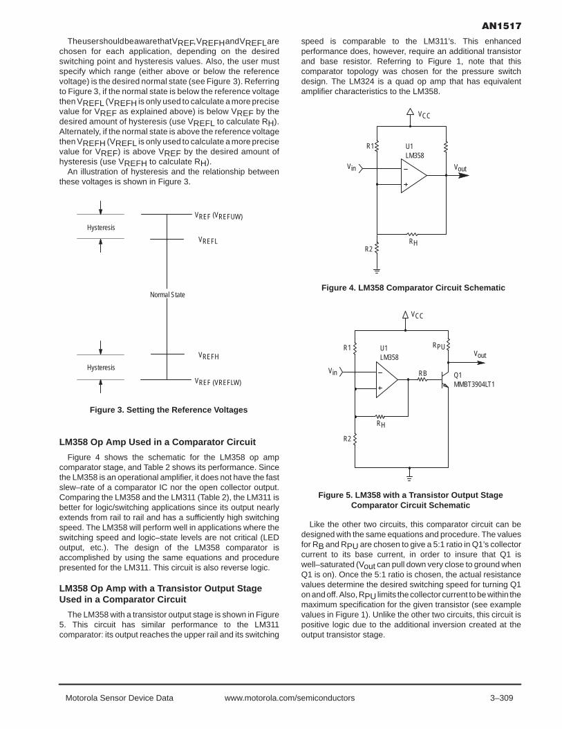
3–309Motorola Sensor Device Data www.motorola.com/semiconductors
The user should be aware that VREF, VREFH and VREFL arechosen for each application, depending on the desiredswitching point and hysteresis values. Also, the user mustspecify which range (either above or below the referencevoltage) is the desired normal state (see Figure 3). Referringto Figure 3, if the normal state is below the reference voltagethen VREFL (VREFH is only used to calculate a more precisevalue for VREF as explained above) is below VREF by thedesired amount of hysteresis (use VREFL to calculate RH).Alternately, if the normal state is above the reference voltagethen VREFH (VREFL is only used to calculate a more precisevalue for VREF) is above VREF by the desired amount ofhysteresis (use VREFH to calculate RH).
An illustration of hysteresis and the relationship betweenthese voltages is shown in Figure 3.
VREF (VREFUW)
VREFL
Hysteresis
Hysteresis
VREFH
VREF (VREFLW)
Normal State
Figure 3. Setting the Reference Voltages
LM358 Op Amp Used in a Comparator Circuit
Figure 4 shows the schematic for the LM358 op ampcomparator stage, and Table 2 shows its performance. Sincethe LM358 is an operational amplifier, it does not have the fastslew–rate of a comparator IC nor the open collector output.Comparing the LM358 and the LM311 (Table 2), the LM311 isbetter for logic/switching applications since its output nearlyextends from rail to rail and has a sufficiently high switchingspeed. The LM358 will perform well in applications where theswitching speed and logic–state levels are not critical (LEDoutput, etc.). The design of the LM358 comparator isaccomplished by using the same equations and procedurepresented for the LM311. This circuit is also reverse logic.
LM358 Op Amp with a Transistor Output StageUsed in a Comparator Circuit
The LM358 with a transistor output stage is shown in Figure5. This circuit has similar performance to the LM311comparator: its output reaches the upper rail and its switching
speed is comparable to the LM311’s. This enhancedperformance does, however, require an additional transistorand base resistor. Referring to Figure 1, note that thiscomparator topology was chosen for the pressure switchdesign. The LM324 is a quad op amp that has equivalentamplifier characteristics to the LM358.
Figure 4. LM358 Comparator Circuit Schematic
RHR2
Vin
R1
Vout
U1LM358
VCC
Figure 5. LM358 with a Transistor Output StageComparator Circuit Schematic
RH
R2
Vin
R1 RPUVout
U1LM358
RB Q1MMBT3904LT1
VCC
Like the other two circuits, this comparator circuit can bedesigned with the same equations and procedure. The valuesfor RB and RPU are chosen to give a 5:1 ratio in Q1’s collectorcurrent to its base current, in order to insure that Q1 iswell–saturated (Vout can pull down very close to ground whenQ1 is on). Once the 5:1 ratio is chosen, the actual resistancevalues determine the desired switching speed for turning Q1on and off. Also, RPU limits the collector current to be within themaximum specification for the given transistor (see examplevalues in Figure 1). Unlike the other two circuits, this circuit ispositive logic due to the additional inversion created at theoutput transistor stage.
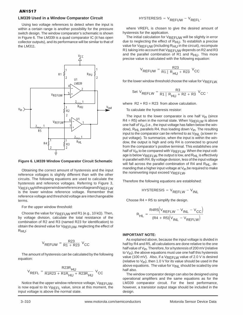
3–310 Motorola Sensor Device Datawww.motorola.com/semiconductors
LM339 Used in a Window Comparator Circuit
Using two voltage references to detect when the input iswithin a certain range is another possibility for the pressureswitch design. The window comparator’s schematic is shownin Figure 6. The LM339 is a quad comparator IC (it has opencollector outputs), and its performance will be similar to that ofthe LM311.
Figure 6. LM339 Window Comparator Circuit Schematic
+
+
VinVout
U1LM339
VCC
RPUR1
RHUR2
R4 R3RHL
VREFLW
R5
VREFUW
1
2
1
2
2
1
2 11
2
1
2
2 1
4
5
6
7
1
2
2
1
U1
Obtaining the correct amount of hysteresis and the inputreference voltages is slightly different than with the othercircuits. The following equations are used to calculate thehysteresis and reference voltages. Referring to Figure 3,VREFUW is the upper window reference voltage and VREFLWis the lower window reference voltage. Remember thatreference voltage and threshold voltage are interchangeableterms.
For the upper window threshold:
Choose the value for VREFUW and R1 (e.g., 10 kΩ). Then,by voltage division, calculate the total resistance of thecombination of R2 and R3 (named R23 for identification) toobtain the desired value for VREFUW, neglecting the effect ofRHU:
VREFUW R23R1R23
VCC
The amount of hysteresis can be calculated by the followingequation:
VREFL R23RHU
R1R23R1RHUR23RHUVCC
Notice that the upper window reference voltage, VREFUW,is now equal to its VREFL value, since at this moment, theinput voltage is above the normal state.
HYSTERESIS VREFUW VREFL,
where VREFL is chosen to give the desired amount ofhysteresis for the application.
The initial calculation for VREFUW will be slightly in errordue to neglecting the effect of RHU. To establish a precisevalue for VREFUW (including RHU in the circuit), recomputeR1 taking into account that VREFUW depends on R2 and R3and the parallel combination of R1 and RHU. This moreprecise value is calculated with the following equation:
VREFUW R23R1 RHUR23
VCC
for the lower window threshold choose the value for VREFLW.
Set VREFLW R3R1 RHUR2 R3
VCC ,
where R2 + R3 = R23 from above calculation.
To calculate the hysteresis resistor:
The input to the lower comparator is one half Vin (sinceR4 = R5) when in the normal state. When VREFLW is aboveone half of Vin (i.e., the input voltage has fallen below the win-dow), RHL parallels R4, thus loading down Vin. The resultinginput to the comparator can be referred to as VINL (a lower in-put voltage). To summarize, when the input is within the win-dow, the output is high and only R4 is connected to groundfrom the comparator’s positive terminal. This establishes onehalf of Vin to be compared with VREFLW. When the input volt-age is below VREFLW, the output is low, and RHL is effectivelyin parallel with R4. By voltage division, less of the input voltagewill fall across the parallel combination of R4 and RHL, de-manding that a higher input voltage at Vin be required to makethe noninverting input exceed VREFLW.
Therefore the following equations are established:
HYSTERESIS VREFLW VINL
Choose R4 = R5 to simplify the design.
RHL R4R5VREFLW VINL VCC
(R4R5)VINL VREFLW
IMPORTANT NOTE:As explained above, because the input voltage is divided in
half by R4 and R5, all calculations are done relative to the onehalf value of Vin. Therefore, for a hysteresis of 200 mV (relativeto Vin), the above equations must use one half this hysteresisvalue (100 mV). Also, if a VREFLW value of 2.0 V is desired(relative to Vin), then 1.0 V for its value should be used in theabove equations. The value for VINL should be scaled by onehalf also.
The window comparator design can also be designed usingoperational amplifiers and the same equations as for theLM339 comparator circuit. For the best performance,however, a transistor output stage should be included in thedesign.

3–311Motorola Sensor Device Data www.motorola.com/semiconductors
TEST/CALIBRATION PROCEDURE
1. Before testing the circuit, the user–defined values forRTH, RH and Roff should be calculated for the desiredapplication.
The sensor offset voltage is set by
VoffVoff
R1RoffVCC .
Then, the amplified sensor voltage corresponding to a givenpressure is calculated by
Vsensor = 201 x 0.0002 x APPLIED PRESSURE + Voff,
where 201 is the gain, 0.0002 is in units of V/kPa andAPPLIED PRESSURE is in kPa.
The threshold voltage, VTH, at which the output changesstate is calculated by determining Vsensor at the pressure thatcauses this change of state:
RTHR7 RTH
VCC .
VTH = Vsensor (@ pressure threshold) =
If hysteresis is desired, refer to the LM311 Used in aComparator section to determine RH.
2. To test this design, connect a +5 volt supply between pins3 and 4 of the connector CN1.
3. Connect a volt meter to pins 1 and 4 of CN1 to measurethe output voltage and amplified sensor voltage,respectively.
4. Connect an additional volt meter to the VTH probe pointto verify the threshold voltage.
5. Turn on the supply voltage.6. With no pressure applied, check to see that Voff is correct
by measuring the voltage at the output of the gain stage(the volt meter connected to Pin 4 of CN1). If desired, Voffcan be fine tuned by using a potentiometer for Roff.
7. Check to see that the volt meter monitoring VTH displaysthe desired voltage for the output to change states. Use apotentiometer for RTH to fine tune VTH, if desired.
8. Apply pressure to the sensor. Monitor the sensor’s outputvia the volt meter connected to pin 4 of CN1. The outputwill switch from low to high when this pressure sensorvoltage reaches or exceeds the threshold voltage.
9. If hysteresis is used, with the output high (pressuresensor voltage greater than the threshold voltage), checkto see if VTH has dropped by the amount of hysteresisdesired.
A potentiometer can be used for RH to fine tune theamount of hysteresis.
CONCLUSION
The pressure switch design uses a comparator to create alogic level output by comparing the pressure sensor outputvoltage and a user–defined reference voltage. The flexibilityof this minimal component, high performance design makesit compatible with many different applications. The designpresented here uses an op amp with a transistor output stage,yielding excellent logic–level outputs and output transitionspeeds for many applications. Finally, several othercomparison stage designs, including a window comparator,are evaluated and compared for overall performance.
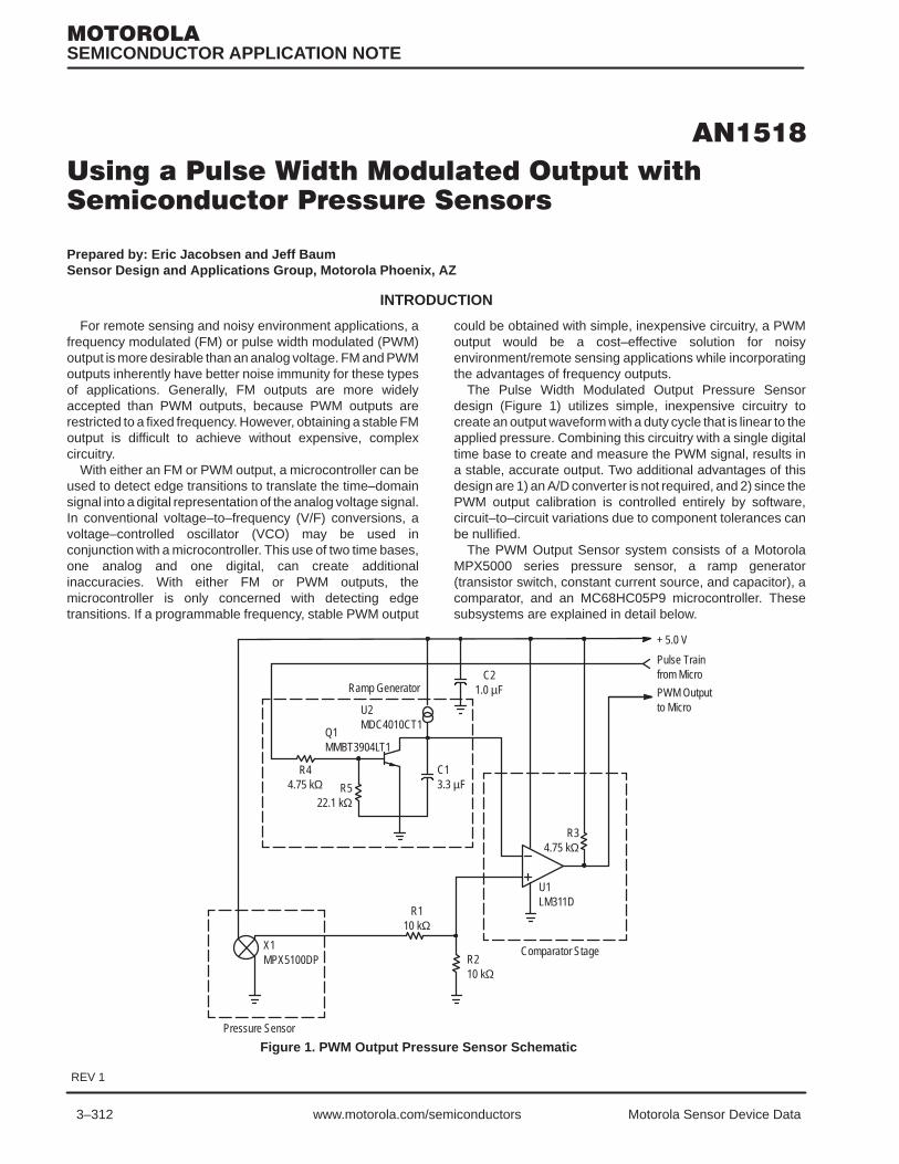
3–312 Motorola Sensor Device Datawww.motorola.com/semiconductors
Prepared by: Eric Jacobsen and Jeff BaumSensor Design and Applications Group, Motorola Phoenix, AZ
INTRODUCTION
For remote sensing and noisy environment applications, afrequency modulated (FM) or pulse width modulated (PWM)output is more desirable than an analog voltage. FM and PWMoutputs inherently have better noise immunity for these typesof applications. Generally, FM outputs are more widelyaccepted than PWM outputs, because PWM outputs arerestricted to a fixed frequency. However, obtaining a stable FMoutput is difficult to achieve without expensive, complexcircuitry.
With either an FM or PWM output, a microcontroller can beused to detect edge transitions to translate the time–domainsignal into a digital representation of the analog voltage signal.In conventional voltage–to–frequency (V/F) conversions, avoltage–controlled oscillator (VCO) may be used inconjunction with a microcontroller. This use of two time bases,one analog and one digital, can create additionalinaccuracies. With either FM or PWM outputs, themicrocontroller is only concerned with detecting edgetransitions. If a programmable frequency, stable PWM output
could be obtained with simple, inexpensive circuitry, a PWMoutput would be a cost–effective solution for noisyenvironment/remote sensing applications while incorporatingthe advantages of frequency outputs.
The Pulse Width Modulated Output Pressure Sensordesign (Figure 1) utilizes simple, inexpensive circuitry tocreate an output waveform with a duty cycle that is linear to theapplied pressure. Combining this circuitry with a single digitaltime base to create and measure the PWM signal, results ina stable, accurate output. Two additional advantages of thisdesign are 1) an A/D converter is not required, and 2) since thePWM output calibration is controlled entirely by software,circuit–to–circuit variations due to component tolerances canbe nullified.
The PWM Output Sensor system consists of a MotorolaMPX5000 series pressure sensor, a ramp generator(transistor switch, constant current source, and capacitor), acomparator, and an MC68HC05P9 microcontroller. Thesesubsystems are explained in detail below.
Figure 1. PWM Output Pressure Sensor Schematic
PWM Outputto Micro
+ 5.0 V
Pulse Trainfrom Micro
Comparator Stage
Ramp Generator
Pressure Sensor
U1LM311D
C21.0 µF
R522.1 kΩ
R44.75 kΩ
Q1MMBT3904LT1
C13.3 µF
U2MDC4010CT1
R110 kΩ
R34.75 kΩ
X1MPX5100DP R2
10 kΩ
SEMICONDUCTOR APPLICATION NOTE
REV 1

3–313Motorola Sensor Device Data www.motorola.com/semiconductors
PRESSURE SENSOR
Motorola’s MPX5000 series sensors are signal conditioned(amplified), temperature compensated and calibrated (i.e.,offset and full–scale span are precision trimmed) pressuretransducers. These sensors are available in full–scalepressure ranges of 50 kPa (7.3 psi) and 100 kPa (14.7 psi).With the recommended 5.0 V supply, the MPX5000 series
produces an output of 0.5 V at zero pressure to 4.5 V at fullscale pressure. Referring to the schematic of the system inFigure 1, note that the output of the pressure sensor isattenuated to one–half of its value by the resistor dividercomprised of resistors R1 and R2. This yields a span of 2.0 Vranging from 0.25 V to 2.25 V at the non–inverting terminal ofthe comparator. Table 1 shows the electrical characteristics ofthe MPX5100.
Table 1. MPX5100DP Electrical Characteristics
Characteristic Symbol Min Typ Max Unit
Pressure Range POP 0 — 100 kPa
Supply Voltage VS — 5.0 6.0 Vdc
Full Scale Span VFSS 3.9 4.0 4.1 V
Zero Pressure Offset Voff 0.4 0.5 0.6 V
Sensitivity S — 40 — mV/kPa
Linearity — – 0.5 — 0.5 %FSS
Temperature Effect on Span — –1.0 — 1.0 %FSS
Temperature Effect on Offset — – 50 0.2 50 mV
THE RAMP GENERATOR
The ramp generator is shown in the schematic in Figure 1.A pulse train output from a microcontroller drives the rampgenerator at the base of transistor Q1. This pulse can beaccurately controlled in frequency as well as pulse duration viasoftware (to be explained in the microcontroller section).
The ramp generator uses a constant current source tocharge the capacitor. It is imperative to remember that thiscurrent source generates a stable current only when it hasapproximately 2.5 V or more across it. With less voltageacross the current source, insufficient voltage will cause thecurrent to fluctuate more than desired; thus, a designconstraint for the ramp generator will dictate that the capacitorcan be charged to only approximately 2.5 V, when using a5.0 V supply.
The constant current charges the capacitor linearly by thefollowing equation:
V ItC
(1)
where ∆t is the capacitor’s charging time and C is thecapacitance.
Referring to Figure 2, when the pulse train sent by themicrocontroller is low, the transistor is off, and the currentsource charges the capacitor linearly. When the pulse sent bythe microcontroller is high, the transistor turns on intosaturation, discharging the capacitor. The duration of the highpart of the pulse train determines how long the capacitordischarges, and thus to what voltage it discharges. This is howthe dc offset of the ramp waveform may be accuratelycontrolled. Since the transistor saturates at approximately60 mV, very little offset is needed to keep the capacitor fromdischarging completely.
Figure 2. Ideal Ramp Waveform for the PWM Output Pressure Sensor
MicrocontrollerPulse Train
Exaggerated Capacitor Discharge
RampWaveform
Ramp WaveformOffset (100 mV)

3–314 Motorola Sensor Device Datawww.motorola.com/semiconductors
The PWM output is most linear when the ramp waveform’speriod consists mostly of the rising voltage edge (seeFigure 2). If the capacitor were allowed to completelydischarge (see Figure 3), a flat line at approximately 60 mVwould separate the ramps, and these “flat spots” may result in
non–linearities of the resultant PWM output (after comparingit to the sensor voltage). Thus, the best ramp waveform isproduced when one ramp cycle begins immediately afteranother, and a slight dc offset disallows the capacitor fromdischarging completely.
Exaggerated Capacitor Discharge
Figure 3. Non Ideal Ramp Waveform for the PWM Output Pressure Sensor
MicrocontrollerPulse Train
RampWaveform
The flexibility of frequency control of the ramp waveform viathe pulse train sent from the microcontroller allows aprogrammable–frequency PWM output. Using Equation 1 thefrequency (inverse of period) can be calculated with a givencapacitor so that the capacitor charges to a maximum ∆V ofapproximately 2.5 V (remember that the current source needsapproximately 2.5 V across it to output a stable current). Theimportance of software control becomes evident here sincethe selected capacitor may have a tolerance of ± 20%. Byadjusting the frequency and positive width of the pulse train,the desired ramp requirements are readily obtainable; thus,nullifying the effects of component variances.
For this design, the ramp spans approximately 2.4 V from0.1 V to 2.5 V. At this voltage span, the current source is stableand results in a linear ramp. This ramp span was used forreasons which will become clear in the next section.
In summary, complete control of the ramp is achieved by thefollowing adjustments of the microcontroller–created pulsetrain:
• Increase Frequency: Span of ramp decreases.The dc offset decreases slightly.
• Decrease Frequency: Span of ramp increases. The dc offset increases slightly.
• Increase Pulse Width: The dc offset decreases. Span decreases slightly.
• Decrease Pulse Width: The dc offset increases. Span increases slightly.
THE COMPARATOR STAGE
The LM311 chip is designed specifically for use as acomparator and thus has short delay times, high slew rate,and an open–collector output. A pull–up resistor at the outputis all that is needed to obtain a rail–to–rail output. As Figure 1shows, the pressure sensor output voltage is input to thenon–inverting terminal of the op amp and the ramp is input tothe inverting terminal. Therefore, when the pressure sensorvoltage is higher than a given ramp voltage, the output is high;likewise, when the pressure sensor voltage is lower than agiven ramp voltage, the output is low (refer to Figure 5). Asmentioned in the Pressure Sensor section, resistors R1 andR2 of Figure 1 comprise the voltage divider that attenuates thepressure sensor’s signal to a 2.0 V span ranging from 0.25 Vto 2.25 V.
Since the pressure sensor voltage does not reach theramp’s minimum and maximum voltages, there will be a finiteminimum and maximum pulse width for the PWM output.These minimum and maximum pulse widths are designconstraints dictated by the comparator’s slew rate. Thesystem design ensures a minimum positive and negativepulse width of 20 µs to avoid nonlinearities at the high and lowpressures where the positive duty cycle of the PWM output isat its extremes (refer to Figure 4 ). Depending on the speed ofthe microcontroller used in the system, the minimum requiredpulse width may be larger. This will be explained in the nextsection.

3–315Motorola Sensor Device Data www.motorola.com/semiconductors
THE MICROCONTROLLER
The microcontroller for this application requires inputcapture and output compare timer channels. The outputcapture pin is programmed to output the pulse train that drivesthe ramp generator, and the input capture pin detects edgetransitions to measure the PWM output pulse width.
Since software controls the entire system, a calibrationroutine may be implemented that allows an adjustment of thefrequency and pulse width of the pulse train until the desiredramp waveform is obtained. Depending on the speed of themicrocontroller, additional constraints on the minimum andmaximum PWM output pulse widths may apply. For thisdesign, the software latency incurred to create the pulse train
at the output compare pin is approximately 40 µs.Consequently, the microcontroller cannot create a pulse trainwith a positive pulse width of less than 40 µs. Also, thesoftware that measures the PWM output pulse width at theinput capture pin requires approximately 20 µs to execute.Referring to Figure 5, the software interrupt that manipulatesthe pulse train always occurs near an edge detection on theinput capture pin (additional software interrupt). Therefore, theminimum PWM output pulse width that can be accuratelydetected is approximately 60 µs (20 µs + 40 µs). Thisconstrains the minimum and maximum pulse widths morethan the slew rate of the comparator which was discussedearlier (refer to Figure 4).
Figure 4. Desired Relationship Between the Ramp Waveform and Pressure Sensor Voltage Spans
∆V Sets MinimumPulse Width (60 µs)
VSFS
VSOFF
∆V Sets MaximumPulse Width (Period – 60 µs)
An additional consideration is the resolution of the PWMoutput. The resolution is directly related to the maximumfrequency of the pulse train. In our design, 512 µs are requiredto obtain at least 8–bit resolution. This is determined by thefact that a 4 MHz crystal yields a 2 MHz clock speed in themicrocontroller. This, in turn, translates to 0.5 µs per clock tick.There are four clock cycles per timer count. This results in 2 µsper timer count. Thus, to obtain 256 timer counts (or 8–bitresolution), the difference between the zero pressure and fullscale pressure PWM output pulse widths must be at least512 µs (2 µs x 256). But since an additional 60 µs is neededat both pressure extremes of the output waveform, the totalperiod must be at least 632 µs. This translates to a maximumfrequency for the pulse train of approximately 1.6 kHz. Withthis frequency, voltage span of the ramp generator, and valueof current charging the capacitor, the minimum capacitor valuemay be calculated with Equation 1.
To summarize:The MC68HC705P9 runs off a 4 MHz crystal. The
microcontroller internally divides this frequency by two to yieldan internal clock speed of 2 MHz.
12 MHz
0.5 s
clock cycle
And,4 clock cycles = 1 timer count.
Therefore,
4 clock cyclestimer count
0.5 s
clock cycle
2 stimer count
For 8–bit resolution,
2 stimer count
256 counts 512 s
Adding a minimum of 60 µs each for the zero and full scalepressure pulse widths yields
512 µs + 60 µs + 60 µs = 632 µs,which is the required minimum pulse train period to drive theramp generator.
Translating this to frequency, the maximum pulse trainfrequency is thus
1632 s
1.58 kHz.

3–316 Motorola Sensor Device Datawww.motorola.com/semiconductors
CALIBRATION PROCEDURE AND RESULTS
The following calibration procedure will explain how tosystematically manipulate the pulse train to create a ramp thatmeets the necessary design constraints. The numbers usedhere are only for this design example. Figure 6 shows thelinearity performance achieved by following this calibrationprocedure and setting up the ramp as indicated by Figures 4and 5.1. Start with a pulse train that has a pulse width and
frequency that creates a ramp with about 100 mV dcoffset and a span smaller than required. In this examplethe initial pulse width is 84 µs and the initial frequency is1.85 kHz.
2. Decrease the frequency of the pulse train until the rampspan increases to approximately 2.4 V. The ramp span of
2.4 V will ensure that the maximum pulse width at fullscale pressure will be at least 60 µs less than the totalperiod. Note that by decreasing the frequency of thepulse train, a dc offset will begin to appear. This mayresult in the ramp looking nonlinear at the top.
3. If the ramp begins to become nonlinear, increase thepulse width to decrease the dc offset.
4. Repeat steps 2 and 3 until the ramp spans 2.4 V and hasa dc offset of approximately 100 mV. The dc offset valueis not critical, but the bottom of the ramp should have a“crisp” point at which the capacitor stops discharging andbegins charging. Simply make sure that the minimumpulse width at zero pressure is at least 60 µs. Refer toFigures 4 and 5 to determine if the ramp is sufficient forthe application.
Figure 5. Relationships Between the PWM Output Pressure Sensor Voltages
MicrocontrollerPulse Train
Exaggerated Capacitor Discharge
RampWaveform
Ramp WaveformOffset (100 mV)
SensorVoltage
PWM OutputVoltage
Figure 6. PWM Output Pressure Sensor Linearity Data
Pressure (kPa)
100
90
80
70
60
50
40
30
20
10
0
65060055050045040035030025020015010050
00 20 40 60 80 100
Duty CyclePulse Width
Dut
y C
ycle
(%)
Puls
e W
idth
( s
)µ

3–317Motorola Sensor Device Data www.motorola.com/semiconductors
CONCLUSION
The Pulse Width Modulated Output Pressure Sensor usesa ramp generator to create a linear ramp which is comparedto the amplified output of the pressure sensor at the input ofa comparator. The resulting output is a digital waveform witha duty cycle that is linearly proportional to the input pressure.Although the pressure sensor output has a fixed offset and
span, the ramp waveform is adjustable in frequency, dc offset,and voltage span. This flexibility enables the effect ofcomponent tolerances to be nullified and ensures that rampspan encompasses the pressure sensor output range. Theramp’s span can be set to allow for the desired minimum andmaximum duty cycle to guarantee a linear dynamic range.
3–318 Motorola Sensor Device Datawww.motorola.com/semiconductors
! !
Prepared by: Eric Jacobsen and Jeff BaumSensor Applications Engineering Motorola Signal Products Division Phoenix, AZ
INTRODUCTION
Although fully signal–conditioned, calibrated, andtemperature compensated monolithic sensor IC’s arecommercially available today, there are many applicationswhere the flexibility of designing custom signal–conditioningis of great benefit. Perhaps the need for a versatile low–levelsensor output is best illustrated by considering two particularcases that frequently occur: (1) the user is in a prototypingphase of development and needs the ability to make changesrapidly to the overall transfer function of the combinedsensor/amplifier subsystem, (2) the specific desired transferfunction does not exist in a fully signal–conditioned,precision–trimmed sensor product (e.g., a signal–conditioneddevice is precision trimmed over a different pressure rangethan that of the application of interest). In such cases, it isobvious that there will always be a need for low–level,nonsignal–conditioned sensors. Given this need, there is alsoa need for sensor interface amplifier circuits that can signalcondition the “raw” sensor output to a usable level. Thesecircuits should also be user friendly, simple, and cost effective.
Today’s unamplified solid–state sensors typically have anoutput voltage of tens of millivolts (Motorola’s basic 10 kPapressure sensor, MPX10, has a typical full–scale output of58 mV, when powered with a 5 V supply). Therefore, a gainstage is needed to obtain a signal large enough for additionalprocessing. This additional processing may includedigitization by a microcontroller’s analog to digital (A/D)converter, input to a comparator, etc. Although thesignal–conditioning circuits described here are applicable tolow–level, differential–voltage output sensors in general, thefocus of this paper will be on interfacing pressure sensors toamplifier circuits.
This paper presents a basic two operational–amplifiersignal–conditioning circuit that provides the desiredcharacteristics of an instrumentation amplifier interface:
• High input impedance
• Low output impedance
• Differential to single–ended conversion of the pressuresensor signal
• High gain capability
For this two op–amp circuit, additional modifications to thecircuit allow (1) gain adjustment without compromisingcommon mode rejection and (2) both positive and negative dclevel shifts of the zero pressure offset. Varying the gain andoffset is desirable since full–scale span and zero pressureoffset voltages of pressure sensors will vary somewhat fromunit to unit. Thus, a variable gain is desirable to fine tune thesensor’s full–scale span, and a positive or negative dc levelshift (offset adjustment) of the pressure sensor signal isneeded to translate the pressure sensor’s signal–conditionedoutput span to a specific level (e.g., within the high and lowreference voltages of an A/D converter).
For the two op–amp gain stage, this paper will present thederivation of the transfer function and simplified transferfunction for pressure sensor applications, the derivation andexplanation of the gain stage with a gain adjust feature, andthe derivation and explanation of the gain stage with the dclevel shift modification.
Adding another amplifier stage provides an alternativemethod of creating a negative dc voltage level shift. Thisstage is cascaded with the output from the two op–amp stage(Note: gain of the two op–amp stage will be reduced due toadditional gain provided by the second amplifier stage). Forthis three op–amp stage, the derivation of the transferfunction, simplified transfer function, and the explanation ofthe negative dc level shift feature will be presented.
GENERAL NOTE ON OFFSET ADJUSTMENT
Pressure sensor interface circuits may require either apositive or a negative dc level shift to adjust the zero pressureoffset voltage. As described above, if the signal–conditionedpressure sensor voltage is input to an A/D, the sensor’soutput dynamic range must be positioned within the high andlow reference voltages of the A/D; i.e., the zero pressureoffset voltage must be greater than (or equal to) the lowreference voltage and the full–scale pressure voltage mustbe less than (or equal to) the high reference voltage (seeFigure 1). Otherwise, voltages above the high reference willbe digitally converted as 255 decimal (for 8–bit A/D), andvoltages below the low reference will be converted as 0. Thiscreates a nonlinearity in the analog–to–digital conversion.
SEMICONDUCTOR APPLICATION NOTE

3–319Motorola Sensor Device Data www.motorola.com/semiconductors
Figure 1. Positioning the Sensor’s Full–Scale Span within the A/D’s or Amplifier’s Dynamic Range
A/D HIGH REFERENCE OR HIGH SATURATION LEVEL OF AMPLIFIER
FULL–SCALEOUTPUT VOLTAGE
A/D LOW REFERENCE OR LOWSATURATION LEVEL OF AMPLIFIER
ZERO PRESSUREOFFSET VOLTAGE
SEN
SOR
’S F
ULL
–SC
ALE
VOLT
AGE
SPAN
A/D
’S O
R A
MPL
IFIE
R’S
DYN
AMIC
RAN
GE
A similar requirement that warrants the use of a dc levelshift is the prevention of the pressure sensor’s voltage fromextending into the saturation regions of the operationalamplifiers. This also would cause a nonlinearity in the sensoroutput measurements. For example, if an op–amp poweredwith a single–ended 5 V supply saturates near the low rail ofthe supply at 0.2 V, a positive dc level shift may be requiredto position the zero pressure offset voltage at or above 0.2 V.Likewise, if the same op–amp saturates near the high rail ofthe supply at 4.8 V, a negative dc level shift may be requiredto position the full–scale pressure voltage at or below 4.8 V.It should be obvious that if the gain of the amplifiers is toolarge, the span may be too large to be positioned within the4.6 V window (regardless of ability to level shift dc offset). Insuch a case, the gain must be decreased to reduce the span.
THE TWO OP–AMP GAIN STAGETRANSFER FUNCTION
The transfer function of the two op–amp signal–conditioningstage, shown in Figure 2, can be determined using nodalanalysis at nodes 1 and 2. The analysis can be simplified bycalculating the transfer function for each of the signals with theother two signals grounded (set to zero), and then employingsuperposition to realize the overall transfer function. As shownin Figure 2, VIN2 and VIN1 are the differential amplifier inputsignals (with VIN2 > VIN1), and VREF is the positive dc leveladjust point. For a sensor with a small zero pressure offsetand operational amplifiers powered from a single–endedsupply, it may be necessary to add a positive dc level shift tokeep the operational amplifiers from saturating near zerovolts.
Figure 2. The Two Operational–Amplifier Gain Stage
VIN2
VIN1
VREF
NODE 1
R1
R2 R4
R3
VCC
NODE 2
U1VO′
VO
U1

3–320 Motorola Sensor Device Datawww.motorola.com/semiconductors
First, the transfer function for VIN1 is determined bygrounding VREF and VIN2 at node 1:
VIN1R1
= VO′ – VIN1
R2(1)
and at node 2:
VO′
R3 = –
VOR4
(2)
By solving Equations (1) and (2) for VO′ and equating theresults, Equation (3) is established:
R2R1
1 VIN1 = – R3R4
VO(3)
Solving for VO yields
VO1 = – R4R3R2
R1 1 VIN1 (4)
where VO1 represents the part of VO that VIN1 contributes.To determine the transfer function for VIN2, VIN1 and VREF
are grounded, and a similar analysis is used, yielding
VO2 =R4R3
1 VIN2 (5)
where VO2 represents the part of VO that VIN2 contributes.Finally, to calculate the transfer function between VO and
VREF, VIN1 and VIN2 are grounded to obtain the followingtransfer function:
VOREF = R4R2R3R1
VREF (6)
where VOREF represents the part of VO that VREFcontributes.
Using superposition for the contributions of VIN1, VIN2, andVREF gives the overall transfer function for the signal–conditioning stage.
VO = VO1 + VO2 + VOREF
VO = – R4R3R2
R1 1 VIN1 +R4
R3 1 VIN2
+ R4R2R3R1
VREF (7)
Equation (7) is the general transfer function for thesignal–conditioning stage. However, the general form is notonly cumbersome, but also if no care is taken to match certainresistance ratios, poor common mode rejection results. Asimplified form of this equation that provides good commonmode rejection is shown in the next section.
APPLICATION TO PRESSURESENSOR CIRCUITS
The previous section showed the derivation of the generaltransfer function for the two op–amp signal–conditioningcircuit. The simplified form of this transfer function, as appliedto a pressure sensor application, is derived in this section.
For pressure sensors, VIN1 and VIN2 are referred to as S–and S+, respectively. The simplification is obtained by setting
R4R3
= R1R2
Through this simplification, Equation (7) simplifies to
VO = R4R3
1 ( S+ – S–) + VREF (8)
By examining Equation (8), the differential gain of thesignal– conditioning stage is:
G = R4R3
+ 1 (9)
Also, since the differential voltage between S+ and S– is thepressure sensor’s actual differential output voltage(VSENSOR), the following equation is obtained for VO:
VO = R4R3
1 VSENSOR + VREF (10)
Finally, the term VREF is the positive offset voltage added tothe amplified sensor output voltage. VREF can only be positivewhen using a positive single–ended supply. This offset (dclevel shift) allows the user to adjust the absolute range that thesensor voltage spans. For example, if the gain established byR4 and R3 creates a span of four volts and this signal swingis superimposed upon a dc level shift (offset) of 0.5 volts, thena signal range from 0.5 V to 4.5 V results.
VREF is typically adjusted by a resistor divider as shown inFigure 3. A few design constraints are required whendesigning the resistor divider to set the voltage at VREF.
• To establish a stable positive dc level shift (VREF), VCCshould be regulated; otherwise, VREF will vary as VCC va-ries.
• When “looking” into the resistor divider from R1, the effec-tive resistance of the parallel combination of the resistors,RREF1 and RREF2, should be at least an order of magni-tude smaller than R1’s resistance. If the resistance of theparallel combination is not small in comparison to R1, R1’svalue will be significantly affected by the parallel combina-tion’s resistance. This effect on R1 will consequently affectthe amplifier’s gain and reduce the common mode rejec-tion.

3–321Motorola Sensor Device Data www.motorola.com/semiconductors
Figure 3. A Resistor Divider to Create V REF
R1VREF TO U1
VCC
RREF1
RREF2
THE TWO OP–AMP GAIN STAGE WITHVARIABLE GAIN
Varying the gain of the two op–amp stage is desirable forfine–tuning the sensor’s signal–conditioned output span.However, to adjust the gain in the two op–amp gain circuit inFigure 2 and to simultaneously preserve the common moderejection, two resistors must be adjusted. To adjust the gain,it is more desirable to change one resistor. By adding anadditional feedback resistor, RG, the gain can be adjusted withthis one resistor while preserving the common mode rejection.Figure 4 shows the two op–amp gain stage with the addedresistor, RG.
Figure 4. Two Operational–Amplifier Gain Stage withVariable Gain
VIN2
VIN1
VREF
NODE 1
R1
R2 R4
R3
VCC
NODE 2
U1
VO
U1
RG
VO′
As with the two op–amp gain stage, nodal analysis andsuperposition are used to derive the general transfer functionfor the variable gain stage.
VO =R4R3
R4RG
R2R4R3RG
1 VIN2
–R4R3
R4RG
R2R4R3RG
R2R4R1R3 VIN1
+ R2R4R1R3 VREF (11)
This general transfer function also is quite cumbersomeand is susceptible to producing poor common mode rejection
without additional constraints on the resistor values. To obtaingood common mode rejection, use a similar simplification asbefore; that is, set
R1 = R4
and
R2 = R3
Defining the voltage differential between VIN2 and VIN1 asVSENSOR, the simplified transfer function is
VO = R4R3
2R4RG
1 (VSENSOR) + VREF (12)
Thus, the gain is
G = R4R3
+ 2R4RG
+ 1 (13)
and VREF is the positive dc level shift (offset).
Use the following guidelines when determining the value forRG:
• By examining the gain equation, RG’s resistance shouldbe comparable to R4’s resistance. This will allow fine tun-ing of the gain established by R4 and R3. If RG is too large(e.g., RG approaches ∞), it will have a negligible effect onthe gain. If RG is too small (e.g., RG approaches zero), theRG term will dominate the gain expression, thus prohibit-ing fine adjustment of the gain established via the ratio ofR4 and R3.
• Use a potentiometer for RG that has a resistance range onthe order of R4 (perhaps with a maximum resistance equalto the value of R4). If a fixed resistor is preferable to a poten-tiometer, use the potentiometer to adjust the gain, measurethe potentiometer’s resistance, and replace the potentiom-eter with the closest 1% resistor value.
• To maintain good common mode rejection while varyingthe gain, RG should be the only resistor that is varied. RGequally modifies both of the resistor ratios which need to bewell–matched for good common mode rejection, thus pre-serving the common mode rejection.
THE TWO OP–AMP GAIN STAGE WITH VARIABLEGAIN AND NEGATIVE DC LEVEL SHIFT
The last two op–amp circuits both incorporate positive dclevel shift capability. Recall that a positive dc level shift isrequired to keep the operational amplifiers from saturatingnear the low rail of the supply or to keep the zero pressureoffset above (or equal to) the low reference voltage of an A/D.This two op–amp stage incorporates an additional resistor,ROFF, to provide a negative dc level shift. A negative dc levelshift is useful when the zero pressure offset voltage of thesensor is too high. In this case, the user may be required tolevel shift the zero pressure offset voltage down (toward zerovolts). Now, for a specified amount of gain, the full–scalepressure output voltage does not saturate the amplifier at thehigh rail of the voltage supply, nor is it greater than the A/D’shigh reference voltage. Figure 5 shows the schematic for thisamplifier circuit.

3–322 Motorola Sensor Device Datawww.motorola.com/semiconductors
Figure 5. Two Op–Amp Signal–Conditioning Stage with Variable Gain and Negative Dc Level Shift Adjust
VIN2
VIN1
VREF
NODE 1
R1
R2 R4
R3
VCC
NODE 2
U1VO′
VO
U1
RG
ROFF
To derive the general transfer function, nodal analysis andsuperposition are used:
VO =R4R3
R4RG
R2R4R3RG
1 VIN2
– R4R3
R4RG
R2R4R1R3
R2R4R3RG VIN1
+ R2R4R1R3 VREF +
R4ROFF
(VIN2 – VCC) (14)
As before, defining the sensor’s differential output asVSENSOR, defining VIN2 as S+ for pressure sensorapplications, and using the simplification that
R1 = R4
and
R2 = R3
obtains the following simplified transfer function:
VO = R4R3
2R4RG
1 (VSENSOR) + VREF
+ R4
ROFF (S+ – VCC) (15)
The gain is
G = R4R3
+ 2R4RG
+ 1 (16)
To adjust the gain, refer to the guidelines presented in thesection on Two Op–Amp Gain Stage with Variable Gain.
VREF is the positive dc level shift, and the negative dc levelshift is:
V–shift = R4
ROFF (S+ – VCC) (17)
The following guidelines will help design the circuitry for thenegative dc voltage level shift:
• To establish a stable negative dc level shift, VCC should beregulated; otherwise, the amount of negative level shift willvary as VCC varies.
• ROFF should be the only resistor varied to adjust thenegative level shift. Varying R4 will change the gain of thetwo op–amp circuit and reduce the common mode rejec-tion.
• To determine the value of ROFF:1. Determine the amount of negative dc level shifting re-
quired (defined here as V–shift).2. R4 already should have been determined to set the gain
for the desired signal–conditioned sensor output.3. Although V–shift is dependent on S+, S+ changes only
slightly over the entire pressure range. With Motorola’sMPX10 powered at a 5 V supply, S+ will have a value ofapproximately 2.51 V at zero pressure and will increaseas high as 2.53 V at full–scale pressure. This error overthe full–scale pressure span of the device is negligiblewhen considering that many applications use an 8–bitA/D converter to segment the pressure range. Using an8–bit A/D, the 20 mV (0.02 V) error corresponds to only1 bit of error over the entire pressure range (1 bit / 255bits x 100% = 0.4% error).
4. ROFF is then calculated by the following equation:
ROFF = S+ – VCC
V–shift
R4 (18)
An alternative to using this equation is to use apotentiometer for ROFF that has a resistance range on theorder of R4 (perhaps 1 to 5 times the value of R4). Use thepotentiometer to fine tune the negative dc level shift, whilemonitoring the zero pressure offset output voltage, VO. Asbefore, if a fixed resistor is preferable, then measure thepotentiometer’s resistance and replace the potentiometerwith the closest 1% resistor value.
Important note: The common mode rejection of this amplifiertopology will be low and perhaps unacceptable in someapplications. (A SPICE model of this amplifier topologyshowed the common mode rejection to be 28 dB.) However,this circuit is presented as a solution for applications whereonly two operational amplifiers are available and the commonmode rejection is not critical when considering the required

3–323Motorola Sensor Device Data www.motorola.com/semiconductors
system performance. Adding a third op–amp to the circuit forthe negative dc level shifting capability (as shown in the nextsection) is a solution that provides good common moderejection, but at the expense of adding an additional op–amp.
THE THREE OP–AMP GAIN STAGEFOR NEGATIVE DC LEVEL SHIFTING
This circuit adds a third op–amp to the output of the twoop–amp gain block (see Figure 6). This op–amp has a dualfunction in the overall amplifier circuit:
• Its non–inverting configuration provides gain via the ratioof R6 and R5.
• It has negative dc voltage level shifting capability typicallycreated by a resistor divider at V–shift, as discussed in thesection on Application to Pressure Sensor Circuits. Al-though this configuration requires a third op–amp for thenegative dc level shift, it has no intrinsic error nor low com-mon mode rejection associated with the negative level shift(as does the previous two op–amp stage). Depending onthe application’s accuracy requirement, this may be a moredesirable configuration for providing the negative dc levelshift.
First, use the same simplifications as before; that is, set
R1 = R4
and
R2 = R3
Defining the voltage differential between VIN2 and VIN1 asVSENSOR , the simplified transfer function is
VO = 1 R6R5 R4
R3
2R4RG
1VSENSOR
+ VREF – R6R5
V–shift (20)
The gain is
G =1 R6R5 R4
R3
2R4RG
1 (21)
VREF is the positive dc level shift (offset), and V–shift is thenegative dc level shift.
Figure 6. Three Op–Amp Gain Stage with Variable Gain and Negative Dc Level Shift
VIN2
VIN1
VREFR1
R2 R4
R3
VCC
U1VO′
U1
RG
VO″
VO
V–SHIFTR5 R6
U1
The transfer function for this stage will be similar to thechosen two op–amp gain stage configuration (either the fixedgain with positive dc level shift circuit or the variable gain withpositive dc level shift circuit) with additional terms for thenegative level shift and gain. As an example, the variable–gaintwo op–amp gain circuit is used here. All of the designconsiderations and explanations for the variable gain twoop–amp circuit apply.
The transfer function may be derived with nodal analysisand superposition.
VO =1 R6R5 R4
R3
R4RG
R2R4R3RG
1 VIN2
– R4R3
R4RG
R2R4R3RG
R2R4R1R3
VIN1
+ R2R4R1R3
VREF – R6R5
V–shift (19)
The preceding simplifications have been performed in theprevious sections, but by examining Equation 20, notice thatthe third op–amp’s gain term also amplifies the positive andnegative dc voltage level shifts, VREF and V–shift. If R6 and R5are chosen to make an arbitrary contribution to the overallsystem gain, designing an appropriate amount of positive andnegative dc level shift can be difficult. To simplify the transferfunction, set R5 = R6, and the following equation for VO results:
VO = 2R4R3
2R4RG
1VSENSOR VREF
– V–shift (22)
Now the third op–amp’s contribution to the overall systemgain is a factor of two. When designing the overall system gainand the positive dc level shift, use the following guidelines:

3–324 Motorola Sensor Device Datawww.motorola.com/semiconductors
• Since the third op–amp contributes a gain of two to theoverall system, design the gain that the two op–amp circuitcontributes to the system to be one–half the desired sys-tem gain. The gain term for the two op–amp circuit is:
G = R4R3
+2R4RG
+ 1
which is the same as presented in Equation 16.
• Similarly, since the third op–amp also amplifies VREF bytwo (refer to Equation 22), the resistor divider that createsVREF should be designed to provide one–half the desiredpositive dc voltage level shift needed for the final output.When designing the voltage divider for VREF, use the samedesign constraints as were given in the section on Applica-tion to Pressure Sensor Circuits.
With the above simplification of R5 = R6, the negative dclevel shift, V–shift, which is also created by a voltage divider, isnow amplified by a factor of unity. When designing the voltagedivider, use the same design constraints as were presented inthe section on Application to Pressure Sensor Circuits.
CONCLUSION
The amplifier circuits discussed in this paper apply topressure sensor applications, but the amplifier circuits can beinterfaced to low–level, differential–voltage output sensors, ingeneral. All of the circuits exhibit the desired instrumentationamplifier characteristics of high input impedance, low outputimpedance, high gain capability, and differential tosingle–ended conversion of the sensor signal. Eachamplifier circuit provides positive dc level shift capability, whilethe last two circuit topologies presented are also able toprovide a negative dc voltage level shift. This enables the userto position the sensor’s dynamic output within a specifiedrange (e.g., within the high and low references of an A/Dconverter). Also detailed is a method of using an additionalfeedback resistor to adjust easily the differential voltage gain,while not sacrificing common mode rejection. Combining theappropriate sensor device and amplifier interface circuitprovides sensor users with a versatile system solution forapplications in which the ideal fully single–conditioned sensordoes not exist or in which such signal flexibility is warranted.

3–325Motorola Sensor Device Data www.motorola.com/semiconductors
Prepared by: Bill LucasIndustrial Technology Center
INTRODUCTION
This application note describes a Digital Boat Speedometerconcept which uses a monolithic, temperature compensatedsilicon pressure sensor, analog signal–conditioning circuitry,microcontroller hardware/software and a liquid crystal display.This sensing system converts water head pressure to boatspeed. This speedometer design using a 30 psi pressuresensor (Motorola P/N: MPXM2202GS) yields a speed rangeof 5 mph to 45 mph. Calibration of the system is performedusing data programmed into the microcontroller’s internalmemory.
A key advantage in all Motorola pressure sensors is thepatented X–ducer , a single piezoresistive implant thatreplaces the traditional Wheatstone bridge configuration usedby competitors. In addition to the X–ducer, Motorola integrateson–chip all necessary temperature compensation, eliminat-ing the need for separate substrates/hybrids. This state–of–the–art technology yields superior performance andreliability. Motorola pressure sensors are offered in severaldifferent port configurations to allow measurement ofabsolute, differential and gauge pressure. Motorola offersthree pressure sensor types: uncompensated, temperaturecompensated and calibrated or fully signal conditioned.
WATER PRESSURE TO BOAT SPEEDCONVERSION
A typical analog boat speedometer employs a pitot tube, acalibrated pressure gauge/speedometer and a hose toconnect the two. The pitot tube, located at the boat transom,provides the pressure signal corresponding to boat speed.This pressure signal is transmitted to the gauge via the hose.Boat speed is related to the water pressure at the pitot tube asdescribed by the following equation:
P e * (V22g)
where:V = speedP = pressure at pitot tubee = specific weight of mediag = gravitational acceleration
For example, to calculate P in lb/in2 for an ocean applicationuse:
V = speed in mphe = 63.99 lbs/ft3 at 60°F, seawater
(e will be smaller for fresh water)g = 32 ft/sec2
15 mph = 22 ft/sec1 ft2 = 144 in2
P (63.99[lbft3] 144[in2ft2]) (V2[mph]2
(2215)2[(ftsec)mph]2 2 (32.2)[ftsec2])
P[PSI] V8.208
2For example, if the boat is cruising at 30 mph, the impactpressure on the pitot tube is:
P (308.208)2 13.36 psi.
DIGITAL BOAT SPEEDOMETER DESCRIPTIONAND OPERATION
The MPXM2202GS senses the impact water pressureagainst the pitot tube and outputs a proportional differentialvoltage signal. This differential voltage signal is then fed (viaan analog switch and gain circuitry) to a single slopeanalog–to–digital converter (A/D) which is external to themicrocontroller. The A/D circuit can complete two separateconversions as well as a reference conversion simultaneous-ly. This A/D utilizes the microcontroller’s internal timers ascounters and software to properly manipulate the data. Theanalog switch provides a way to flip the sensor outputs afteran A/D conversion step, which is necessary to null out theoffset effects of the op–amps. This is accomplished byperforming an analog conversion, reversing the sensor’sdifferential output signal, performing another analog conver-sion, summing the two readings, then dividing this sum by two.Any op–amp offset present will be the same polarityregardless of the sensor output polarity, thus the op–ampoffset can be mathematically nulled out. The digitalrepresentation of any analog signal is ratiometric to thereference voltages of the A/D converter. Also, the sensor’soutput is ratiometric to its excitation voltage. Therefore, if boththe sensor and A/D reference voltages are connected to thesame unregulated supply, the variations in sensor output willbe nullified, and system accuracy will be maintained (i.e.,systems in which both the A/D converter’s digital value — dueto variations in the A/D’s reference voltages — and sensor’soutput voltage are ratiometric to the supply voltage so that avoltage regulator is not necessary).
SEMICONDUCTOR APPLICATION NOTE

3–326 Motorola Sensor Device Datawww.motorola.com/semiconductors
Figure 1 shows the pressure sensor (XDCR) connected tothe analog switches of the 74HC4053 which feeds thedifferential signal to the first stage of op–amps. An A/Dconversion is performed on the two op–amp output signals,Vout1 and Vout2. The difference (Vout1 – Vout2) is com-puted and stored in microcontroller memory. The analogswitch commutates (op–amp connections switch from Y0 andZ0 to Y1 and Z1), reversing the sensor output signals to the twoop–amps, and another conversion is performed. This value isthen also stored in the microcontroller memory. To summarize,via software, the following computation takes place:
Step 1: Vfirst = Vout1 – Vout2Step 2: Vsecond = Vout2 – Vout1Step 3: Vresult = (Vfirst + Vsecond) / 2
Again, because any op–amp offset will remain the samepolarity regardless of sensor output polarity, this routine willeffectively cancel any amplifier offset. Any offset the sensormay introduce is compensated for by software routines thatare invoked when the initial system calibration is done.
The single slope A/D provides 11 or more unsigned bits ofresolution. This capability provides a water pressureresolution to at least 0.05 psi. This translates to a boat speedresolution of 0.1 mph over the entire speed range.
Figure 2 describes the pressure versus voltage transferfunction of the first op–amp stage.
Figure 1. X–ducer, Instrument Amplifier and Analog Switch
+
–33078
–
+33078
MPXM2202GS 74HC4053Y0
Y1
Z0
Z1
3 2
4 1
2
1
5
3
11 12 13 9 10
+ 8
+
–
876 16
+ 5
15
4
5
3
2
6 7
1
8
4
+ 8
VOUT1
VOUT2
DENOTES ANALOG GROUND
DENOTES LOGIC GROUNDXDCR INPUT REVERSE CONTROL
10 k
10 k22 pF
22 pF
316 k
316 k10 k
Figure 2. Instrument Amplifier Transfer Function
8
6
4
2
00 10 20 30 PSI
PRESSURE IN
U3–1 (U3–7)
VOLT
S O
UT
U3–7 (U3–1)
Figure 3 details the analog circuitry, microcontroller’s timercapture registers and I/O port which comprise the single slopeA/D. The microcontroller’s 16–bit free running counter is alsoemployed, but not shown in the figure.
Comparators U6A, U6B and U6D of the LM139A are usedto provide the A/D function. Constant current source, U7,resistors R13 and R14 and diode D2 provide a linear voltageramp to the inverting inputs of U6, with about 470 microampscharge current to capacitor C8, with transistor Q1 in the offstate. C8 will charge to 5 volts in about 5 milliseconds at thegiven current. Q1 is turned on to provide a discharge path forC8 when required. The circuit is designed such that when thevoltage to the inverting inputs of the comparators exceeds thevoltage to the noninverting comparators, each comparatoroutput will trip from a logic 1 to a logic 0.
One A/D conversion consists of the following steps:(1) setting the pressure sensor output polarity (via softwareand the analog switches of U4) to the amplifier inputs of theMC33078 (U3), (2) reading the value of the free running

3–327Motorola Sensor Device Data www.motorola.com/semiconductors
counter, (3) turning off Q1, and (4) charging C8 and waiting forthe three (U6) comparator outputs to change from 1 to 0.When the comparator outputs change state, themicrocontroller free running counter value is clocked into themicrocontroller’s input capture register. Contained in thisregister then is the number of counts required to charge C8 toa value large enough to trip the comparators. Via software, thevoltage signal from U3 (corresponding to the applied pressuresignal) can be compared to the “reference.”
The boat speed display for this design employs anMC145453 LCD driver and four–digit liquid crystal display, ofwhich three digits and a decimal point are used. Figure 4shows the connections between the display driver and thedisplay. The display driver is connected to themicroprocessor’s serial peripheral interface (SPI). Thesoftware necessary to initialize, format and drive the LCD isincluded in the software listing contained in this article.
Figure 3. Analog–to–Digital Converter Front End with Microcontroller
–
+LM139A
–
+LM139A
–
+LM139A
INPUT CAPTUREREGISTER 1
GENERAL PURPOSEOUTPUT
INPUT CAPTUREREGISTER 2
INPUT CAPTUREREGISTER 3
+8
LM334Z–3
U7 D2 (APPROX. 470 µA)
1N914
R13147 Ω
R141.5 k5%
R124.7 Ω5%
2N7000 Q1
C80.47 µF
POLYCARBONATE
10
11
8
9
4
5
13
14
2
32
27
33
34
+ 5
R1010 k5%
R1110 k5%
+83
1/4 U6C
R910 k5%
1/4 U6B
1/4 U6A
FROM U3–7
FROM U3–1
12
VREF(APPROX. 4.5 V)
IC1 (PA2)
PA7
IC2 (PA1)
IC3 (PA0)
MC68HC711E9
+5

3–328M
otorola Sensor D
evice Data
ww
w.m
otorola.com/sem
iconductors
Figure 4. B
oat Speedom
eter Display B
oard
LCD
LIQUID CRYSTAL DISPLAY IEE PART NUMBER LCD5657 OR EQUAL
26 37 36 5 6 7 34 35 8 31 32 9 10 11 29 30 12 26 27 13 14 15 24 25 16 22 23 17 18 19 20 21 1
19 18 17 16 15 14 13 11 10 9 8 7 6 5 4 3 44 43 42 41 40 39 38 37 36 35 33 32 31 30 29 28 27
NC
BP
26 22
21
2
+5
R1470 k
C1470 pF
OSCIN
VSS
VCCOUTIN
DATA BIT
U1 MC145453FN
DATA CLOCK
25 24
1
2
3
4
CLOCK
DATA
+
GND
5VDD
VSS
C20.1

3–329Motorola Sensor Device Data www.motorola.com/semiconductors
Table 1 lists the jumper wire selections needed forcalibration and operational modes. The jumper wire junctionblock (J1, J2, J3) is connected to the microprocessor, pinsPC0, PC1 and PC2, respectively as shown in Figure 5.
Table 1.
J1 J2 J3
OUT OUT OUT Display speed in mph
OUT OUT IN 100 psi X–ducer installed
OUT IN OUT 30 psi X–ducer installed
OUT IN IN 15 psi X–ducer installed
IN OUT OUT Full scale calibrate
IN OUT IN Zero calibrate
IN IN OUT Display pressure in psi
IN IN IN Display speed in mph
Figure 5. Boat Speedometer Processor Board
–
+
+
–
–
+LM139A
–
+
–
+
–
+
+ 8
LM334Z–3U7
R13147 Ω
D2 (APPROX. 470 µA)POLYCARBONATE
C80.47 µF
R141.5 k5%
R124.7 Ω5%
2N7000 Q1
LM139A
LM139A
LM139A
33078
33078
+ 8
10
11
8
9
4
5
31/4 U6
1/4 U6
1/4 U6
VREF + 5
R1110 k5%
R1010 k5%
R910 k5%
+ 5
13
14
2
R410 k5%
R810 k5%
+ 8
5
6
81/2 U3
715
234
1/2 U34
C14 22 pF
C13 22 pF
R5 316 k
R7 316 kR610 k
+ 5
16876
109131211
U4
Y0
Y1
Z0
Z1
2
1
5
3
+ 8
3 2
4 1
74HC4053
6
7
1/4 U6
+ 12
GND
5
6
D1
1N4004
R14.7 Ω
5%
C10.1
C233 µF
+
MC78L05ACPU2
MC78L08ACPU1
VREF(APPROX. 4.5 V)
C710 µF
+C60.1
C410 µF
+C30.1
+ 5
+ 8
R21.15 k
R31.5 k
C50.1
NOTES:UNLESS OTHERWISE NOTED, ALL RESISTORS 1% METAL FILM.
* U5 PINS 11–16 (PC2–PC7) ARE CONNECTED HERE FOR* TERMINATION PURPOSES.
32
27
43
33
34
45
42
52
51
47
49
44
46
48
50
VREF
7
8
17
2
18
19
26
11*
10
9
1
31
3
20
21
22
25
4
24
23
R15 R16R173–10 k5%
IC1 (PA2)
PA7
PE0
IC2 (PA1)
IC3 (PA0)
PE1
PB0
VRH
VRL
PE2
PE3
PE4
PE5
PE6
PE7
XTAL
EXTAL
RESET
MODB
XIRQ
IRQ
VDD
PC2
PC1
PC0
VSSPA3
MODA
PD0
PD1
PD2
PD5
STRA
(PD4) SCK
(PD3) MOSI
R1910 MEG
5% Y18 MHz
C1222 pF
+ 5
+ 5
R184.7 k
5% MC34064P–5U8
J3
J2
J1TEST
JUMPERS
1
23
4
+ 5C100.1
U5
MC68HC711E9FN
MPXM2202GS

3–330 Motorola Sensor Device Datawww.motorola.com/semiconductors
The calibration of this system is as follows. Refer to Table 1.CAUTION: While installing or changing the proper jumpers
described by each step, power must be off. Reapply power toread the display after jumpers have been installed in theirproper location for each step. In each step there is a fewseconds’ delay after switching the power on and before anoutput is displayed. Steps 1 through 3 must be performed priorto system being operational.
Calibration1. The pressure range of the system must be established.
The present software installed in this design supports 15,30 and 100 psi sensors. Using an MPXM2202GS sensor(30 psi) for example, only jumper J2 should be installed.After power is applied, the LCD should read “30.” Poweroff the system prior to proceeding to step 2.
2. The total system offset, due to the sensor and A/D, mustbe established for the software routine to effectivelycalibrate. With power off, jumpers J1 and J3 should beinstalled. Reapply power, and the LCD should respond
with “000.” The offset value measured in this step is thusstored for use in circuit operation. Power off the systemprior to proceeding to step 3.
3. In this step, the system full scale span is calibrated. Withpower off, install jumper J1 only. Now apply the full ratedpressure (30 psi for MPXM2202GS) to the sensor, poweron and ensure the display reads “FFF.” The full scalespan measured in this step is thus stored for use in circuitoperation. Power off the system prior to step 4.
Operation4. Ensure power is off, and install jumpers J1, J2 and J3.
The system is now ready for operation. Simply applypower and pressure to the sensor, and the LCD willdisplay the proportional speed above 5 mph, up to thelimits of the sensor.
REFERENCES
Burry, Michael (1989). “Calibration–Free Pressure SensorSystem,” Motorola Application Note AN1097.

3–331Motorola Sensor Device Data www.motorola.com/semiconductors
NOTE. THIS WAS COMPILED WITH A COMPILER COURTESY OF:INTROL CORP.9220 W. HOWARD AVE.MILWAUKEE, WI. 53228 PHONE (414) 327–7734.
SOME SOURCE CODE CHANGES MAY BE NECESSARY FOR COMPILATION WITH OTHER COMPILERS.THE HEADER FILE io6811.h HAS I/O PORT DEFINITIONS FOR THE I/O PORTS PARTICULAR TO THE MC68HC711E9. A TYPICAL ENTRY FOR
PORT A WILL FOLLOW. THE FIRST LINE ESTABLISHES A BASE ADDRESS BY WHICH ALL I/O FACILITIES AND COUNTERS ARE BIASED.REFER TO THE MC68HC711E9 DATA FOR MORE INFORMATION RELATIVE TO I/O AND TIMER ADDRESSES.
#define IOBIAS 0x1000 /* BASE ADDRESS OF THE I/O FOR THE 68HC11 */#define PORTA (* (char *) (IOBIAS + 0)) /* PORT A */
THE STARTUP ROUTINE NEED ONLY LOAD THE STACK TO THE TOP OF RAM, ZEROTHE MICROCONTROLLER’S RAM AND PERFORM A BSR MAIN (BRANCH TO SUBROUTINE “MAIN”).THIS SOURCE CODE, HEADER FILE, COMPILED OBJECT CODE, AND LISTING FILES ARE AVAILABLE ON:
THE MOTOROLA FREEWARE LINE AUSTIN, TX. (512) 891–3733. Bill Lucas 6/21/90THE CODE STARTS HERE */ #include <io6811.h> /* I/O port definitions */
/* define locations in the eeprom to store calibration information */#define EEPROM (char*)0xb600 /* used by calibration functions */#define EEBASE 0xb600 /* start address of the eeprom */#define ADZERO (* ( long int *)( EEBASE + 0 )) /* auto zero value */#define HIATOD (* ( long int *)( EEBASE + 4 )) /* full scale measured input */#define XDCRMAX (* ( char *)( EEBASE + 8 )) /* full scale input of the xdcr */union bytes unsigned long int l; char b[4]; ; /* ADZERO.l for long word ADZERO.b[0]; for byte */
const char lcdtab[] = 95, 6, 59, 47, 102, 109, 125, 7, 127, 111, 0 ;/* lcd pattern table 0 1 2 3 4 5 6 7 8 9 blank */
const int dectable[] = 10000, 1000, 100, 10 ;
char digit[5]; /* buffer to hold results from cvt_bin_dec function */
/* ################################################################### */
/* real time interrupt service routine */
void real_time_interrupt (void) /* hits every 4.096 ms. */ TFLG2 = 0x40; /* clear the interrupt flag */
/* ################################################################### */
/* ################################################################### */
/* write_eeprom(0xA5,EEPROM); write A5h to first byte of EEPROM */void write_eeprom(char data, char *address)
PPROG = 0x16; /* single–byte erase mode */*address = 0xff; /* write anything */PPROG = 0x17; /* turn on programming voltage */
delay();PPROG = 0x0; /* erase complete */
/* now program the data */ PPROG = 0x02; /* set eelat bit */
*address = data; /* write data */PPROG = 0x03; /* set eelat and eepgm bits */delay();PPROG = 0; /* read mode *//* programming complete */
/* ################################################################### */
long int convert(char polarity)

3–332 Motorola Sensor Device Datawww.motorola.com/semiconductors
unsigned int cntr; /* free running timer system counter */unsigned int r0; /* difference between cntr and input capture 1 register */unsigned int r1; /* difference between cntr and input capture 2 register */unsigned int r2; /* difference between cntr and input capture 3 register */unsigned long difference; /* the difference between the upper and lower instrument amplifier outputs */unsigned long int pfs; /* result defined as percent of full scale relative to the reference voltage */
if (polarity == 1) /* set the hc4053 configuration */ PORTB &= 0xfe; /* polarity = 1 means + output of sensor */ else PORTB |= 0x1; /* is connected to the upper opamp */ delay(); /* this will allow the hc4053 to stabilize and the cap to discharge from the previous conversion */ TFLG1=0X07; /* clear the input capture flags */
cntr=TCNT; /* get the current count */ PORTA &= 0X7F; /* turn the fet off */ while ((TFLG1 & 0X7) < 7); /* loop until all three input capture flags are set */
r0 = TIC1 – cntr; /* reference voltage */ r1 = TIC2 – cntr; /* top side of the inst. amp */ r2 = TIC3 – cntr; /* lower side of the inst. amp */ PORTA |= 0X80; /* turn the fet on */ if (polarity == 1) difference = ( r1 + 1000 ) – r2; else difference = ( r2 + 1000 ) – r1; pfs = (difference * 10000) / r0; if (difference > 32767) /* this will cover up the case where the a to d computes a negative value */ pfs=0; return ( pfs );
atod() /* computes the a/d value in terms of % full scale */ unsigned long int x,y,z; x = convert(1); /* normal */ y = convert(0); /* reversed */ z = (x + y)>>1 ; /* 2x difference / 2 */ return(z); /* z is percent of full scale */
integrate() /* returns the a/d value in terms of % full scale and computes offset from calibration values */unsigned long int j;int i;j=0;for (i=0; i<20; ++i) j +=atod(); j = (j/20) – ADZERO; /* null out the xdcr zero input offset */ return(j);
cala2d() /* returns the average of 50 raw a/d conversions this is only used by the calibration functions */unsigned long int j;int i;j=0;for (i=0; i<50; ++i) j +=atod(); j=j/50; return(j);
/* ################################################################### */
cvt_bin_dec ( unsigned int arg )char i;
for ( i=0; i < 6; ++i )

3–333Motorola Sensor Device Data www.motorola.com/semiconductors
digit[i] = 0; /* put blanks in all digit positions */
for ( i=0; i < 4; ++i ) if ( arg >= dectable [i] ) digit[i] = arg /dectable[i]; arg = arg–(digit[i] * dectable[i]); digit[i] = arg;
/* ################################################################### */
delay()int i;for (i=0; i<1000; ++i); /* delay about 15 ms. @ 8 mhz xtal */
/* ################################################################### */
/* set–up i/o for the single slope a/d, initialize the spi port, then initialize the MC145453 for output */ init_io(void)char i;
/* set–up i/o for the a/d */PACTL |= 0X80; /* make pa7 an output */PORTA |= 0X80; /* turn the fet on */PORTB &= 0X7F; /* set–up the HC4053 in the Y0/Z0 connect mode */TCTL2 = 0X2A; /* capture on falling edge for timer capture 0,1,2 */TFLG1 = 0X07; /* clear any pending capture flags */
/* set–up the i/o for the spi subsystem */PORTD=0x2f; /* set output low before setting the direction register */DDRD=0x38; /* ss = 1, sck = 1, mosi = 1 */SPCR=0x51; /* enable spi, make the cpu the master, E clock /4 */
/* initialize the lcd driver */ for (i=0; i<4; ++i) /* four bytes of zeros */ write_spi(0); write_spi (2); /* this creates a start bit and data bit 1 for the next write to the mc145453 */
/* ################################################################### */
/* this is an attempt at the newton square root method */sqrt(unsigned long b)
unsigned long x0,x1;
if ( b < 4 ) b=2; return (b); else x0=4; x1=10; while (x0 != x1) if( (x1–x0) ==1 ) break; x1=x0; x0=(( (b/x0) +x0 ) >> 1 ); b=x0; return (b);
/* ################################################################### */
3–334 Motorola Sensor Device Datawww.motorola.com/semiconductors
write()char i; digit[1]=10; if (digit[2]==0) digit[2]=10; if ( digit[2]==10 && digit[3]==0 ) digit[3]=10; for ( i=1; i<5; ++i ) if (i==4) write_spi((lcdtab[digit[i]])+0x80); else write_spi(lcdtab[digit[i]]); write_spi (2); /* this creates a start bit and data bit 1 for the next write to the mc145453 */
write_spi( char a ) /* write a character to the spi port */
SPDR=a; while ( ! ( SPSR & 0x80 ) ) /* loop until the spif = 1 */ /* ################################################################### */
/* This function is called at power–up and will determine the operation of the system. The user must complete the system configuration prior to setting the jumper in the first or last two configurations in the table or erroneous operation is guaranteed! test/operation jumper configuration: J3 J2 J1 1 = jumper removed
1 1 1 display speed in mph 1 1 0 reserved 1 0 1 30 psi xdcr installed 1 0 0 15 psi xdcr installed 0 1 1 full scale calibrate 0 1 0 zero calibrate 0 0 1 display pressure in psi 0 0 0 display speed in mph */
setconfig()char i;for ( i=0; i<125; ++i ) delay(); /* to let the charge pump come to life wll */i = PORTC & 0x07; /* and off the unused bits */ if ( i == 7 ) display_speed();
if ( i == 6 )setup_error(); /* non–valid pattern output –SE– on display*/
if ( i == 5 ) write_eeprom(30,&XDCRMAX); /* xdcr is 30 psi */ display(30); if ( i == 4 ) write_eeprom(15,&XDCRMAX); /* xdcr is 15 psi */ display(15); if ( i == 3 ) fullscale_calibrate(); if ( i == 2 ) zero_calibrate();
if ( i == 1 ) display_pressure(); else
display_speed();
/* ################################################################### */
display(char d)
3–335Motorola Sensor Device Data www.motorola.com/semiconductors
if (d==30)write_spi(0); /* blank the upper digit */write_spi(0); /* blank the next to upper digit */write_spi(47); /* 3 */write_spi(95); /* 0 */if (d==15)write_spi(0); /* blank the upper digit */write_spi(0); /* blank the next to upper digit */write_spi(6); /* 1 */write_spi(109); /* 5 */
write_spi(2);while(1);
/* ################################################################### */
fullscale_calibrate()int i;long int temp;union bytes average;temp=0; average.l = cala2d(); /* get the average of 50 a/d conversions */
for ( i=0; i<4; ++i) write_eeprom(average.b[i],EEPROM+i+4);
write_spi(0); /* blank the upper digit */write_spi(113); /* F */write_spi(113); /* F */write_spi(113); /* F */write_spi(2);while(1);
/* ################################################################### */
zero_calibrate()int i;long int temp;union bytes average;temp=0;
average.l = cala2d(); /* get the average of 50 a/d conversions */for ( i=0; i<4; ++i)
write_eeprom(average.b[i],EEPROM+i);
write_spi(0); /* blank the upper digit */write_spi(95); /* 0 */write_spi(95); /* 0 */write_spi(95); /* 0 */write_spi(2);while(1);
/* ################################################################### */
/* speed=8.208(square root(%full scale*transducer full scale)) */display_speed()long atod_result;unsigned int j;
while(1)
atod_result = integrate(); /* read the a/d */ atod_result=( (atod_result*10000) / (HIATOD–ADZERO) ) * XDCRMAX;
atod_result=sqrt(atod_result); atod_result=(atod_result*8208)/10000; j=atod_result;

3–336 Motorola Sensor Device Datawww.motorola.com/semiconductors
if (j<50) j=0; cvt_bin_dec ( j ); write();
/* ################################################################### */
/* pressure=%full scale*transducer max pressure */display_pressure()long atod_result;int j;
while(1) atod_result = integrate(); /* read the a/d */ atod_result=( (atod_result*1000) / (HIATOD–ADZERO) ) * XDCRMAX;
j=atod_result/100; cvt_bin_dec ( j ); write();
/* ################################################################### */
setup_error() /* write ”SE” on the display */write_spi(0);write_spi(109); /* S */write_spi(121); /* E */write_spi(0);write_spi(2);while(1);
/* ################################################################### */
main()init_io();setconfig(); /* determine how to function */while(1); /* should never return here except after calibration */

3–337Motorola Sensor Device Data www.motorola.com/semiconductors
Prepared by: Jeffery BaumSystems Engineering Group LeaderSensor Products DivisionMotorola Semiconductor Products SectorPhoenix, AZ
INTRODUCTION
Until recently, low–cost semiconductor pressure sensorswere designed to measure typical full–scale pressures only aslow as 10 kPa (1.5 psi). Of course, “measure” is a relative term.“Measure” is used here to imply that an output of reasonablemagnitude, signal–to–noise ratio, and accuracy is producedby the sensing device. Such sensor products are available invarious levels of integration and package types. Dependingon the level of application customization required and thebudget available, a sensor user may choose from a range oflow–pressure sensor products such as a 10 kPa“bare–element” (uncompensated) device, a 10 kPa calibratedand temperature compensated device, or a fullysignal–conditioned (high–level output), calibrated, andtemperature compensated integrated 10 kPa device. Theseoptions are typically available as well for higher pressuresranging up to 1000 kPa.
What if the sensor user must measure full–scale pressuresthat are two, four, or even ten times lower than whatconventional sensor technology is capable of measuring? “Dosuch applications and customers exist?’’ The answer is “yes”and “yes.” There are many potential customers that requiresuch low–pressure sensing ability, the two applicationexamples discussed here are: (1) heating ventilation andair–conditioning (HVAC) in the context of building controls and(2) water–level sensing in appliance applications such asclothes washing machines.
For the purposes of measuring low pressures, the units ofinches of water (″ H2O) or millimeters of water (mm H2O) willbe used. Typical HVAC applications have a full–scalepressure of 40 mm H2O and washing machines have either300 or 600 mm H2O, depending on the region of the world(Note: just for reference purposes, 10 kPa 40″ H2O 1000mm H2O 1.5 psi).
Of course, a sensor intended for a higher pressure rangethan the one of interest can be used. However, the effect is thatonly a small portion on the device’s dynamic output range isused for the actual operating range. This low–level output maythen be paired up with a larger than ideal amplifier gain. Thus,a poor signal–to–noise ratio is usually the result. Some sensormanufacturers have recently introduced pressure sensorsdesigned for 4″ and 5″ H2O full–scale ranges (approx.100–125 mm H2O). These devices typically employ siliconwith very thinly micromachined diaphragms or other sensingtechnologies that are significantly larger in form factor withoutany additional functionality. Thin diaphragm devices tend to beextremely fragile and unstable. Even in cases where thedevice is sufficiently robust for the intended operating
pressure range, the sensor has very poor overpressurecapability.
Now that the pressure range of interest has beenestablished, the stage has been set to consider the systemsolution that is the enabling technology for achieving suchlow–pressure sensing capability. Also important in presentingthis low–pressure system solution are some of the otherapplication characteristics besides the pressure range. Forexample, the desired pressure resolution, accuracy, availablepower supply voltage, and end–equipment systemarchitecture play a major role in determining theimplementation of this system solution.
DEVELOPMENT HISTORY
For simplicity’s sake, let’s refer to this low–pressure sensingsystem solution as the “smart sensing” or “smart sensorsystem.” One of the key performance advantages of the smartsensor system is that the output of the actual sensing elementis ratiometric (linearly proportional) to the excitation voltageapplied to the sensing element. Since most semiconductorpressure sensors are characterized with a constant voltagepower supply, current excitation will not be discussed.Although a sensor’s operation is specified at a given powersupply voltage, there is some maximum supply that can beapplied, beyond which power dissipation and self–heatingproduce significant output errors or exceed the package’sthermal handling capability. This means that the strategy ofincreasing the sensor’s excitation to improve the sensor’ssensitivity (increase signal output for a given applied pressure)can be done in a dc fashion only up to some maximum supplyvoltage. For Motorola pressure sensors, this limit allows onlyabout a 50% to 60% increase in sensitivity, depending on thespecific device family.
About five years ago, some of my colleagues were workingon pulsing the sensor supply voltage with a conventionalvoltage and very low duty–cycle, sampling–and–holding theresulting output, and then filtering the output to produce a dcsensor output with very low–power consumption. This was theimpetus to consider pulsing a sensor at a much higher thanrecommended voltage and a low duty–cycle (10% or less) forthe purpose of increased sensitivity. It is true that some of thesensor’s parasitic drawbacks, like its zero–pressure offsetvoltage and temperature coefficient of offset, are increased aswell, but some of the sensor’s negative characteristics arelessened. In addition, other sources of error and noise in thesystem are not subjected to the higher amplifier gain thatwould be required if operating the sensor at a conventionalsupply voltage.
SEMICONDUCTOR APPLICATION NOTE

3–338 Motorola Sensor Device Datawww.motorola.com/semiconductors
The Motorola MPX2010 (see Table 1) is a calibrated andtemperature compensated, 10 kPa (full–scale), pressuresensor device. The data sheet specifies a full–scale output of25 mV at a 10 V supply voltage, for an applied pressure of 10kPa. This same device can be pulsed at 40 V at a 10%duty–cycle and produce either 100 mV for the same 10 kPapressure or 25 mV for only 2.5 kPa of pressure. This techniqueallows a four–fold increase in the signal level for the ratedfull–scale pressure of 10 kPa or the ability to maintain thesame signal level for a pressure that is four times lower (2.5kPa).
Although the idea is relatively simple, the key to providing alow–cost smart sensing solution is in both the hardware andsoftware implementation of this system. In the case of themicropower application, having a “stand–alone” analogsensing solution was a key criteria. As such, this design usedmicropower op–amps, analog CMOS switches, gated timers(one to control pulsed sensor excitation and one to controlsample–and–hold function), and capacitivesample–and–hold circuitry. The effect was a very low–currentdrain, micropower sensor solution. Since low–power, ratherthan low–pressure, was the driving design goal, errorsinduced by power supply variation, temperature drift, anddevice–to–device tolerances were not critical. Not that theseissues are not important for all applications, but forlow–pressure sensing, even small temperature drifts, deviceparameter tolerances, and power supply variations causesignificant errors as a percentage of the sensor output signal.
It should be apparent that the “gated–timerpulsing/sample–and–hold” system architecture can beequally well employed to pulse at higher voltages for
increased sensitivity. However, a low–cost MCU can alsoaccomplish the functions of providing a control pulse to aswitching circuit (for the pulsed sensor excitation) andaffecting a synchronized sample–and–hold feature viasoftware control of an on–chip A/D converter. In addition, theMCU has the capability to implement other “smart” featuresthat can lend the additional required accuracy andfunctionality desired for many low–pressure sensingapplications. The system design intended for low–pressureapplications, as well as the performance–enhancing featuresof pulsed excitation for increased sensitivity, signal averaging,software calibration, and software power supply rejection arepresented. The added functionality of intelligentcommunications capability and serial digital output flexibilityare also discussed.
Of course, these features lead to increased performance atconventional, or even high–pressure ranges. Nonetheless,these features have been developed in the context oflow–pressure sensing where the performance benefits are arequisite of the application. Also, driving acceptance of thissystem technology is a much easier task when coupled toproviding a sensing capability and level of functionality that isotherwise not available in the industry today. Who would havesuspected that a viable smart sensing technology would haveresulted from the pursuit of addressing the low–pressuresensing market? Significant pieces of this system solution areprotected intellectual property. Motorola holds several keypatents on using pulsed excitation for semiconductor sensorsand has filed several others regarding other portions andfuture enhancements to this technology.
Table 1. MPX2010 Operating Characteristics (Supply Voltage = 10 Vdc, TA = 25°C unless otherwise noted)
Characteristic Min Typ Max Unit
Pressure Range 0 — 10 kPa
Supply Voltage — 10 16 Vdc
Supply Current — 6.0 — mAdc
Full Scale Span (FSS) 24 25 26 mV
Zero–Pressure Offset –1.0 — 1.0 mV
Sensitivity — 2.5 — mV/kPa
Linearity –1.0 — 1.0 %VFSS
Pressure Hysteresis (0 to 10 kPa) — ±0.1 — %VFSS
Temperature Hysteresis (–40°C to +125°C) — ±0.5 — %VFSS
Temperature Effect on Full Scale Span –1.0 — 1.0 %VFSS
Temperature Effect on Offset (0°C to 85°C) –1.0 — 1.0 mV
Input Impedance 1300 — 2550 Ω
Output Impedance 1400 — 3000 Ω
Response Time (10% to 90%) — 1.0 — ms
Temperature Error Band 0 — 85 °C
Offset Stability — ±0.5 — %VFSS

3–339Motorola Sensor Device Data www.motorola.com/semiconductors
SYSTEM DESIGN
As mentioned in the introduction, the lowest pressuredevices in the Motorola portfolio are rated at a full–scalepressure of 10 kPa (40″ of H2O). The calibrated andtemperature compensated, 10 kPa device (MPX2010) isspecified to operate at a 10 Vdc supply voltage and produce25 mV (nominal) at the full–scale pressure of 10 kPa. Thistranslates to a 0.25 mV/(V*kPa) pressure sensitivity.Additionally, the absolute maximum supply voltage specifiedis 16 Vdc. Thus, the maximum full–scale output signal that canbe achieved without exceeding the maximum supply voltagerating is 40 mV, or 60% greater than the output at the 10 Vdcspecification. So, a 60% increase can be achieved in theoutput signal of the sensor for the 0–10 kPa pressure range,or the same signal level of 25 mV can be preserved over aproportionally lower applied pressure range (i.e., 0–6.25 kPa).The point here is that increasing the dc supply excitation onlyproduces limited improvement in the output signal level.
Much greater gains in output signal level (sensor span) canbe obtained, if it is possible to operate the sensor atsignificantly higher voltages. Since the thermal/powerdissipation limitation imposed by the maximum dc supply
voltage can be avoided by using a pulsed excitation at a lowduty–cycle (on–time) and reasonable period, and secondorder junction effects do not occur until much higher voltages,the sensor output can be greatly increased by operating at amuch higher ac voltage than permitted by the dc counterpartof this same higher voltage. As an example, industrialapplications like HVAC have 24 V commonly available, and wewant to accurately measure pressures below 10″ H2O. Toachieve a 1–2% of full–scale accuracy (based on temperaturedrift errors, system noise, device tolerance, power supplyvariation/rejection, etc.), 9–12 mV is the typical minimumfull–scale span that is the desired target for the pressure rangeof interest. For the MPX2010 pulsed at 24 V, we obtain 15 mVof output for an applied pressure of 10″ H2O (2.5 kPa). Thissame sensor device will only produce 6.25 mV at its normallyspecified supply of 10 V and 2.5 kPa, thus not meeting thesignal–to–noise ratio criteria for a 1–2% accuracyperformance.
This smart sensing solution is intended to sense full–scalepressures below 10″ H2O with 1% of full–scale pressureresolution and better than 2% of full–scale accuracy. Thefollowing subsystems comprise the hardware portion of thissolution (see Figure 1):
Figure 1. Smart Sensing Block Diagram
PRESSURE SENSOR
SIGNALCONDITIONING
SWITCHINGCIRCUITRY
LOW VOLTAGEINHIBIT
8–BITMICROCONTROLLER
5 V ± 5%REGULATOR
POWER SUPPLYREJECTION CIRCUITRY
VPPDoutDinSCLKCS
VCCGnd

3–340 Motorola Sensor Device Datawww.motorola.com/semiconductors
• high–side switch pulsing circuitry
• signal–conditioning amplifier interface with resistors to ad-just the sensor’s amplified, full–scale span and zero–pres-sure offset
• on–chip resources of a complete 8–bit microcontroller(MCU)
• MCU oscillator circuitry (4 MHz)
• 5 V ±5% linear voltage regulator
• low–voltage inhibit (LVI) supervisory voltage monitoring cir-cuit
• resistor divider connected to the sensor’s power supply biasto sense the excitation voltage across the sensorThese subsystems are explained as follows to provide an
understanding of the system design and its intelligent features(refer to Figure 2).
Pulsing CircuitryAs previously mentioned, the sensor’s output is ratiometric
to the excitation voltage across the sensing element; thesensor’s sensitivity increases with increasing supply voltage.Thus, to detect low pressures and minute changes in
pressure, it is desirable to operate the sensor at the highestpossible excitation voltage. The maximum supply voltage atwhich the sensor can reliably operate is determined by one orboth of the following two limitations: (1) maximum allowablesensor die temperature, (2) maximum supply voltageavailable in the sensing application/system.
In terms of thermal/power dissipation, the maximum voltagethat can be supplied to the sensor on a continuous basis isrelatively low compared to that which can be pulsed on thesensor at a low duty–cycle. The average power that isdissipated in the sensor is the square of the average sensorexcitation voltage divided by the input resistance of thesensor. When the sensor’s supply bias is operated in a pulsedfashion, the average excitation voltage is simply the productof the dc supply voltage used and the percent duty–cycle thatthe dc voltage is “on.”
The pulsing circuitry is a high–side switch (two small–signalswitching transistors with associated bias resistors) that iscontrolled via the output compare (TCMP) pin of the MCU. Theoutput compare timer function of the MCU provides alogic–level pulse waveform to the switch that has a 2–msperiod and a 200–µs on–time (Note: this isuser–programmable).
Figure 2. System Schematic
Signal ConditioningEven with pulsing at a relatively high supply voltage, the
pressure sensing element still has a full–scale output that isonly on the order of tens of millivolts. To input this signal to theA/D converter of the MCU, the sensing element output must beamplified to allow adequate digital resolution. A basictwo–operational amplifier signal–conditioning circuit is used toprovide the following desired characteristics of aninstrumentation amplifier interface:
• high input impedance
• low output impedance
• differential to single–ended conversion of the pressure sen-sor signal
• moderate gain capability
Both the nominal gain and offset reference pedestal of thisinterface circuit can be adjusted to fit a given distribution ofsensor devices. Varying the gain and offset reference pedestal

3–341Motorola Sensor Device Data www.motorola.com/semiconductors
is desirable since pressure sensors’ full–scale span andzero–pressure offset voltages will vary somewhat from lot tolot and unit to unit. During software calibration, each sensordevice’s specific offset and full–scale output characteristicswill be stored. Nonetheless, a variable gain amplifier circuit isdesirable to coarsely tune the sensor’s full–scale span, and apositive or negative dc level shift (offset pedestal adjustment)of the pressure sensor signal is needed to translate thepressure sensor’s signal–conditioned output span to aspecific level (e.g., within the high and low reference voltagesof the A/D converter).
MicrocontrollerThe microcontroller performs all of the necessary tasks to
give the smart sensor system the specified performance andintelligent features. The following describes itsresponsibilities:• Creates the control signal to pulse the sensor.
• Samples the pressure sensor’s output.
• Signal averages a programmable number of samples fornoise reduction.
• Samples a scaled–down version of the pressure sensorsupply voltage. Monitoring the power supply voltage allowsthe microcontroller to reject sensor output changes result-ing from power supply variations.
• Uses serial communications interface (SPI) to receive com-mands from and to send sensor information to a masterMCU.
Resistor Divider for Rejection of Supply VoltageVariation
Since the pressure sensor’s output voltage is ratiometric toits supply voltage, any variation in supply voltage will result invariation of the pressure sensor’s output voltage. Byattenuating the supply voltage (since the supply voltage mayexceed the 5 V range of the A/D) with a resistor divider, thisscaled voltage can be sampled by the microcontroller’s A/Dconverter. By sampling the scaled supply voltage, themicrocontroller can compensate for any variances in thepressure sensor’s output voltage that are due to supplyvariations. This technique allows correct pressuredetermination even when the pressure sensor is powered withan unregulated supply.
5 V RegulatorA 5 V ±5% voltage regulator is required for the following
functions:• To provide a stable 5 V for the high voltage reference (VRH)
of the microcontroller’s A/D converter. A stable voltage ref-erence is crucial for sampling any analog voltage signals.
• To provide a stable 5 V for the resistor divider that is usedto level shift the amplified zero–pressure offset voltage.
Low Voltage Inhibit (LVI) CircuitryLow voltage inhibit circuitry is required to ensure proper
power–on–reset (POR) of the microcontroller and to put theMCU in a known state when the supply voltage is decreasedbelow the MCU supply voltage threshold.
SOFTWARE DESCRIPTION
The smart sensor system’s EPROM resident code providesthe control pulse for the sensor’s excitation voltage andperforms calibration with respect to a wide range of excitationvoltages (20 ~ 28 V typically for HVAC). Pressuremeasurement averaging is also incorporated to reduce bothsignal error and noise. In addition, the availability of a serialcommunications interface allows a variety of softwarecommands to be sent to the smart sensor system.
The following brief outline provides a more detaileddescription about the software features included in the smartsensor system.
Software Calibration and Power Supply RejectionOnly six 8–bit words of information are stored both to
calibrate the smart sensor system for a given sensor deviceand to store the relationship between sensor output and powersupply voltage. This information is used to reduce errors dueto device–to–device variations and to reject variations inpower supply voltage that can introduce error into the pressuremeasurement. The sensor’s amplified output at thezero–pressure offset and full–scale pressure are stored ateach of two different supply voltages. In addition, the scaledand digitized representation of the applied supply voltages isstored. Compensating for power supply variation in softwareallows higher performance with lower tolerance, or evenunregulated, supply voltages. For HVAC applications, wherea 24–Vac line voltage will be simply rectified and filtered toprovide a crude 24–Vdc supply, this approach has majorperformance benefits. The impact on applications where aregulated supply is available is that a lower–cost regulator ordc–to–dc converter can be used without compromisingsystem accuracy significantly.
A/D Sample AveragingNoise inherent to the 8–bit A/D successive approximation
conversion method used by the smart sensor accounts for±1–bit resolution. Signal noise, which exhibits a measuredpeak–to–peak range larger in magnitude than 1 bit of A/Dresolution, can be minimized by a sample averagingtechnique.
The current technique uses 16 A/D converted pressuresamples, sums the result, and divides by 16 (the number ofsamples) to get the average:
AVG = ; where n = 16 (1)(an)n
n
1
Assuming a gaussian distribution of noise, this averagingtechnique improves the signal–to–noise ratio (SNR).
Smart Sensor Unit ID and Software RevisionLevel
This solution may be implemented as a single sensingsystem using a nondedicated MCU to provide the sensingfunction and smart features or as a slaved smart sensor (withdedicated sensing MCU) that communicates over a serial busto a master controller or microprocessor (Host). Partidentification and software revision level can also be read onrequest from the master MCU. This information is utilized bythe master MCU to determine what the full–scale pressurerange of a given smart sensor unit is. This allows for multiplesensor units with different pressure ranges to be controlledand sensed from a single master MCU.

3–342 Motorola Sensor Device Datawww.motorola.com/semiconductors
Table 2. Software Command Codes
Function(Command Codes)
Commandfrom Host
Data fromSmart Sensor
Request Pressure $01 $00–$FF
Dynamic Zero $02 —
Undo Dynamic Zero $03 —
Pressure Range $04 TBD
CommunicationThe serial peripheral interface (SPI) is used to communicate
to a master/host MCU. The master MCU initiates all I/O controland sends commands to the slave regarding data requests,calibration, etc. The command codes are parsed at the slavein a look–up table, at which time the corresponding request isserviced via subroutine. Table 2 lists the Master/Slavecommands.Request Pressure Returns the percent of full–scale pressureapplied to the sensor in the form of $00 (0) through $FF (255)and is equivalent to:
Pressure Range (from 0 to 255),
where x FS = Measured Pressure (2)(0 255)
255
(This calculation is performed by the master MCU.)Dynamic Zero Assigns current input pressure as the offsetvalue, in order to use a nonzero pressure as the offsetreference.Undo Dynamic Zero Resets offset to the original stored offset(see Dynamic Zero).Pressure Range Returns a value representing the sensor’sfull–scale pressure range.
Figure 3. SPI Timing Diagram

3–343Motorola Sensor Device Data www.motorola.com/semiconductors
SOFTWARE EXAMPLES
The following example listings show how a user maycommunicate with the smart sensor via a master MCU. Thesoftware example shown assumes that the master MCU is anMC68HC11. Any MCU with the proper I/O functionality willoperate similarly with the smart sensor system.
When using parallel I/O instead of an SPI port to interfacethe smart sensor, the user must “bit bang” the clock and data
out of the parallel I/O, so as to simulate the SPI port. As longas the timing relationships of data and clock follow those ofFigure 3 (see also Table 3), the smart sensor will functionproperly when interfaced to a processor with a parallel typeinterface. In the following two code examples, the sensor unitis interfaced to the master MCU via the SPI port, and thesensor’s CS input is connected to the HC11’s Port D pin 5.
This example is coded in ‘C’ for the MC68HC11:
/* FIRST INITIALIZE THE I/O (INCLUDE A HEADER FILE TO INCLUDE I/O DEFINITIONS) */
void init_io(void)
PORTD = 0X29; /* SS* PD5 = 1, PD3 = 1, PD0 = 1 */
DDRD = 0X3B; /* SS* PD5 = 1, PD3 = 1, PD1 = 1, PD0 = 1 */
SPCR = 0X5E; /* ENABLE THE SPI, MAKE MCU THE MASTR, SCK = E CLK /4 */
/* I/O INITIALIZATION IS COMPLETE */
/* WE NEED A FUNCTION TO WRITE TO AND READ FROM THE SPI */
write_spi(char data)
SPDR = data; /* WRITE THE DATA TO THE SPI DATA PORT */
while( ! (SPSR & 0x80 )); /* WAIT UNTIL DATA HAS SHIFTED OUT OF AND
BACK INTO THE SPI */
return(SPDR): /* RETRIEVE THE RESULTS OF THE LAST COMMAND TO
THE SENSOR AND RETURN */
/* NOW WE NEED TO CALL THE ABOVE */
void main(void)
char rtn_data; /* rtn_data IS THE RETURNED DATA FROM THE SENSOR */
init_io();
while(1) /* JUST LOOP FOREVER */
rtn_data = write_spi(0x01); /* 0x01 IS THE COMMAND TO THE SENSOR
THAT REQUESTS PRESSURE. THE VALUE IN
rtn_data WILL BE IN THE RANGE OF
0..0XFF = 0..100% FULL SCALE PRESSURE THE
SECOND TIME THROUGH THE LOOP. THE INITIAL
TIME THROUGH THE LOOP, THE DATA
RETURNED IS INDETERMINATE */
The next example is coded in assembly for the MC68HC11:
* PORT OFFSETS INTO THE I/O MAP
PORTS EQU $1000 ASSUME THE I/O STARTS AT $1000
PORTD EQU $8
DDRD EQU $9
SPCR EQU $8
SPSR EQU $29
SPDR EQU $2A
ORG $E000
* FIRST INITIALIZE THE I/O
INITIO LDX #PORTS BASE ADDRESS OF THE I/O
LDAA #$29
STAA PORTD,X SS* PD5 = 1, PD3 = 1, PD0 = 1
LDAA #$3B
STAA DDRD,X SS* PD5 = 1, PD3 = 1, PD1 = 1, PD0 = 1
LDAA #$5E
STAA SPCR,X ENABLE THE SPI, MAKE MCU THE MASTR,
* SCK = E CLK /4
RTS I/O INITIALIZATION IS COMPLETE

3–344 Motorola Sensor Device Datawww.motorola.com/semiconductors
*WE NEED A SUBROUTINE TO WRITE TO AND READ FROM THE SPI
*TO CALL THIS ROUTINE LOAD ACCUMULATOR A WITH THE COMMAND DATA
*AND JSR WRITSPI. WHEN THE ROUTINE RETURNS, ACCUMULATOR A
*CONTAINS THE DATA RETURNED FROM THE SENSOR
WRITSPI LDX #PORTS BASE ADDRESS OF THE I/O
STAA SPDR,X SEND THE COMMAND TO THE SENSOR
WRLOOP BRCLR 7,SPSR,WRLOOP LOOP UNTIL THE DATA HAS SHIFTED
OUT OF AND BACK INTO THE SPI
LDAA SPDR,X RETRIEVE THE RESULTS OF THE LAST
COMMAND
* TO THE SENSOR
RTS
* NOW WE NEED TO CALL THE ABOVE */
START JSR INITIO SET–UP THE I/O
LOOP LDAA #$1 1 IS THE COMMAND TO THE SENSOR THAT
* REQUESTS PRESSURE
JSR WRITSPI SEND THE COMMAND TO THE SENSOR.
* ... THE VALUE RETURNED IN ACCUMULATOR A
* WILL BE IN THE RANGE 0..0XFF = 0..100%
* FULL SCALE PRESSURE THE SECOND TIME
* THROUGH THE LOOP. THE INITIAL TIME
* THROUGH THE LOOP, THE DATA RETURNED
IS INDETERMINATE DATA FROM THE SENSOR
BRA LOOP
Table 3. SPI Timing Characteristics
Characteristic Symbol Min Max Unit
Frequency of Operation fOP dc 525 kHz
Cycle Time tSCLK — 1920 ns
Clock (SCLK) Low Time tSCLKL 932 — ns
Dout Data Valid Time tV — 200 ns
Din Setup Time tS 100 — ns
Din Hold Time tH 100 — ns
On–Bus Delay Time tD1 1 — ms
Off–Bus Delay Time tD2 — 50 µs
Chip Select Period tD3 TBD — ms
SERIAL DATA OUTPUT FORMAT
The serial data output is an 8–bit number of value 0–255.This number represents the current applied pressure as apercentage of the full–scale pressure rating of the smartsensor. The master MCU can simply consider an output of “0”to be zero pressure and “255” to be full–scale pressure. Toconvert this number to engineering units, such as inches ofwater (″ H2O), the master MCU must multiply the smart sensoroutput (0–255) by the full–scale pressure of the smart sensorin ″ H2O and then divide (normalize) by 255. See equation 2.
The master MCU can either use an absolute number for thefull–scale pressure of the smart sensor (as indicatedpreviously) or can query each smart sensor that is connectedto the serial bus for its rated pressure range. The lattertechnique allows multiple smart sensors of various full–scalepressure ranges to be communicating with a single masterMCU, without the need for an absolute addressing schemethat contains full–scale pressure information for each sensor.
CONCLUSION
A smart sensing system that achieves high performance forlow–pressure applications has been presented here. The keyperformance advantage of the smart sensor system is that ittakes advantage of the fact that the output of the actualsensing element is ratiometric (linearly proportional) to theexcitation voltage applied to the sensing element. A sensordevice is pulsed at a much higher than normally specifiedvoltage and a low duty–cycle for the purpose of increasedsensitivity. Although some of the sensor’s parasitic drawbacksare increased in magnitude, some of the sensor’s negativecharacteristics are lessened, and other sources of error andnoise in the system are reduced. The net effect is that a bettersignal–to–noise ratio is obtained. This, combined with severalother performance–enhancing smart features, provides betterpressure resolution and accuracy than inherent in the sensordevice alone.
3–345Motorola Sensor Device Data www.motorola.com/semiconductors
Besides the sensor excitation pulsing and output samplingfunctions, a low–cost MCU provides the performance–enhancing features of signal averaging, software calibration,and software power supply rejection. The added–functionalityof intelligent communications capability, serial digital outputflexibility, and local control and decision–making capability arealso at the user’s disposal. The development history, systemdesign, software functions, example communicationsroutines, and serial output format have been detailed to
provide the reader with an understanding of howlow–pressure capability can be greatly enhanced via a smartsensor system approach.
ACKNOWLEDGMENTS
I wish to acknowledge my colleagues Bill Lucas and WarrenSchultz for their outstanding efforts and major contributions tothe pursuit of low–pressure sensing technology.

3–346 Motorola Sensor Device Datawww.motorola.com/semiconductors
!
Prepared by: Eric Jacobsen and Jeff BaumSensor Systems Engineering GroupMotorola Sensor Products DivisionPhoenix, AZ
INTRODUCTION
When designing a circuit for a sensor system, it is desirableto use fixed–value components in the design. This makes thesystem easier and cheaper to produce in high volume. Thealternatives to using fixed–value circuitry are very expensiveand usually impractical: laser–trimming resistances, manuallycalibrating potentiometers, or measuring and selectingspecific component values are all very labor–intensiveprocesses. However, every sensor has device–to–devicevariations in offset output voltage, full–scale output voltage,dynamic output voltage range (difference between thefull–scale output voltage and zero–scale output voltage whichis commonly referred to as the span), etc. Moreover, thesesame parameters also vary with temperature — e.g.,temperature coefficient of offset (TCVoff) and temperaturecoefficient of full–scale span (TCVFSS). To further complicatethis situation, the fixed–value circuit in which a sensor isapplied also has variation — e.g., the voltage or currentregulator and resistors all have a specified tolerance.
Since today’s unamplified solid–state sensors typicallyhave an output voltage on the order of tens of millivolts(Motorola’s basic 10 kPa pressure sensor, MPX10, has atypical full–scale span of 58 mV, when powered with a 5 Vsupply), a major part of the fixed–value circuitry is a gain stagethat amplifies the signal to a level that is large enough foradditional processing. Typically, this additional processing isdigitization of the amplified analog sensor signal by amicrocontroller’s A/D converter. To obtain the best signalresolution with an A/D, the sensor’s amplified dynamic outputvoltage range should fill as much of the A/D window (differencebetween the A/D’s high and low reference voltages) aspossible without extending beyond the high and low referencevoltages (i.e., the zero–pressure offset voltage must begreater than or equal to the low reference voltage, and thefull–scale output voltage must be less than or equal to the highreference voltage). In any case, the device–to–device,temperature, and circuit variations create a design dilemma:with a fixed–value amplifier circuit, the gain as well as any dclevel shift incorporated in the amplifier design are fixed. If thevariation of any of the aforementioned sensor parameters istoo large, the amplified sensor output may saturate theamplifier near either its high or low supply rail or may extendbeyond either the high or low reference voltages of the A/Dconverter. In either case, error (non–linearity) results in the
system. To avoid this scenario, the solution is to design afixed–value circuit that optimizes performance (signalresolution) while taking into account all possible types ofvariation that may cause the sensor output to vary. In otherwords, the goal of this fixed–value sensor system is to attainthe best performance possible while ensuring through design,regardless of any system variation, that the sensor’s amplifiedoutput will ALWAYS be within the saturation levels of theamplifier and the high and low reference voltages of an A/Dconverter.
The implication of ensuring that the sensor’s amplifiedoutput is always unsaturated and within the high and lowreference voltages of the A/D is that an accurate softwarecalibration of the sensor’s output is possible. By sampling thesensor’s output voltage at a couple of points at roomtemperature (zero and full–scale output, for example), all theroom temperature device–to–device and circuit variations arenullified. Obviously, temperature variations will create error inthe system (sensor’s output voltage will drift with changingtemperature), but, by design, the sensor’s output voltage willremain within the A/D’s valid range.
This paper discusses a methodology that optimizes asensor system’s performance while consideringdevice–to–device, temperature, and circuit variations that cancreate variation in the amplified sensor output. Themethodology starts with a desired performance and someestablished parameters and then considers each type ofvariation in a worst case analysis to determine if the desiredperformance is attainable. While this paper discusses thismethodology for pressure sensors and a specific amplifiertopology, the methodology is applicable to low–level,differential–voltage output sensors and amplifier circuits ingeneral. Two specific examples are presented that apply thismethodology. The first example uses Motorola’s MPX10pressure sensor, and the second example uses Motorola’sMPX2010 pressure sensor. Both sensors have a full–scalerated pressure of 10 kPa; the difference between the devicesis the MPX2010 has on–chip calibration and temperaturecompensation circuitry to calibrate and temperaturecompensate the zero–pressure offset voltage and span. Thecomparison of these two devices will emphasize howdramatically device–to–device and temperature variations, ifnot compensated, can affect a system’s overall performance.
SEMICONDUCTOR APPLICATION NOTE

3–347Motorola Sensor Device Data www.motorola.com/semiconductors
THE EXAMPLE CIRCUIT
Referring to Figure 1, both pressure sensors are interfacedto the same amplifier circuit topology. In Tables 1 and 2, therelevant characteristics for the MPX10 and MPX2010 showthe device–to–device and temperature variations.Additionally, the tolerances on the voltage regulator and the
resistors that establish the gain and dc voltage level shift(VREF) are considered in the methodology. The voltageregulator’s device–to–device tolerance is ±5%, and eachresistor’s tolerance is ±1%.
–+ –
+
Vin
5 V REG. (± 5%)IN OUT
GND
VS
RREF1
S –
S +
X1MPX10 OR MPX2010
R1
R2
R3
R4
U1
U1LM33272
VO TO A/D
RREF2
VREF
Figure 1. MPX10/MPX2010 Circuit Schematic
Table 1. MPX10 Variation Characteristics
Characteristic (V S = 5.0 V) Symbol Min Typ Max Unit
Pressure Range POP 0 — 10 kPa
Full–Scale Span VFSS 33 58 83 mV
Zero Pressure Offset Voff 0 33 58 mV
Temperature Coefficient of Full–Scale Span (see Note 1) TCVFSS –0.22 –0.19 –0.16 %/°C
Temperature Coefficient of Offset (see Note 2) TCVoff — ±15 — µV/°C
Note 1: Slope of end–point straight line fit to full–scale span at –40°C and +125°C relative to 25°CNote 2: Slope of end–point straight line fit to zero pressure offset at –40°C and +125°C relative to 25°C
Table 2. MPX2010 Variation Characteristics
Characteristic (V S = 5.0 V) Symbol Min Typ Max Unit
Pressure Range POP 0 — 10 kPa
Full–Scale Span VFSS 12 12.5 13 mV
Zero Pressure Offset Voff –0.5 — 0.5 mV
Temperature Effect on Full–Scale Span (see Note 1) TCVFSS –1.0 — 1.0 %FSS
Temperature Effect on Offset (see Note 2) TCVoff –0.5 — 0.5 mV
Note 1: Maximum change in full–scale span at 0°C and 85°C relative to 25°CNote 2: Maximum change in offset at 0°C and 85°C relative to 25°C
The amplifier topology used is a two–operational amplifiergain stage that has all the desirable characteristics of adifferential–signal instrumentation amplifier:
• high input impedance• low output impedance• differential to single–ended conversion of the input signal• high gain capability• dc level shifting capability
For good common mode rejection, the following resistorratios are used:
R4R3
R1R2
With this simplification, the transfer function of the amplifieris
VO ( R4R3 1) (S – S–) VREF
3–348 Motorola Sensor Device Datawww.motorola.com/semiconductors
Where the gain is (R4R3 1), the pressure sensor’s
differential output voltage is the quantity (S+ – S–), and thepositive dc voltage level shift, created by the voltage dividercomprised of RREF1 and RREF2, is VREF. In addition to usingthe above resistor ratios to preserve the common moderejection, the effective resistance of the parallel combinationof RREF1 and RREF2 should be a low impedance to groundrelative to the resistance of R1.
RESOLUTION AND FACTORS THAT AFFECT IT
Performance of a pressure sensor system is directly relatedto its resolution. Resolution is the smallest increment ofpressure that the system can resolve — e.g., a system thatmeasures pressure up to 10 kPa (full–scale) with a resolutionof 1% of full–scale can resolve pressure increments of0.1 kPa. Similarly, the resolution (smallest increment ofvoltage) of an 8–bit A/D converter with a 5 V window (a highreference voltage of 5 V and a low reference voltage of 0 V) is
5 V255 (8 bits)
19.6 mV
Many pressure sensor systems interface an A/D converter.If the above system example requires 1% resolution wheninterfaced to an A/D, the pressure sensor signal’s span mustbe at least
19.6 mV1%
1.96 V
If the system resolution required is 0.5%, the pressuresensor signal’s span must be at least
19.6 mV0.5%
3.92 V
From these examples, the greater the resolution required,the greater the sensor’s amplified span must be to meet theresolution requirement. Since a pressure sensor’s spanbefore amplification is only on the order of tens of millivolts, theamplifier must be designed to provide the minimum span thatgives the desired resolution. If the amplifier has a fixed gain,any device–to–device variation in the sensor’s unamplifiedspan will result in variation of the amplified span. If, forexample, the sensor’s span variation results in an amplifiedspan that is smaller than required, the resolution of the systemwill not be as high as desired. Alternately, if the sensor’s spanvariation results in an amplified span that is larger thanrequired, the resolution will be better than desired, BUT theamplified span may also either saturate the amplifier near itssupply rails or extend outside the high and low referencevoltages of the A/D. Voltages above the high reference will bedigitally converted as 255 decimal (for 8–bit A/D), and voltagesbelow the low reference will be converted as 0. This createsa non–linearity in the analog–to–digital conversion and in theoverall system transfer function.
As presented above, the variation of the sensor’s spancreates a dilemma: how does one design a fixed–gainamplifier that gives the desired resolution, does not violate the
limits of the linear output ranges of the op–amps and A/Dconverter, and also accommodates the complete distributionof possible sensor spans? The same question is presented tothe additional sources of variation: device–to–device variationin the zero–pressure offset voltage and temperature effects onboth the sensor’s span and zero–pressure offset voltage. Alsoany component tolerances for the voltage regulator andresistors must be considered.
Designing the system when only one source of variation isinvolved is not difficult; however, when all of these variationsare interacting, the solution becomes complicated. The rest ofthis paper describes a design methodology that considers allof the above variations and their interactions. Worst case limitswill be used in designing the fixed–value system.
RESOLUTION vs. HEADROOM
As stated previously, the amplified span of the sensor must“fit” within the high and low references of an A/D to avoid anynonlinearity errors. And the span must also be large enoughto provide the resolution required for the application. Any partof the A/D’s “window” that is not used for the sensor’s dynamicsignal range is called headroom. Headroom may be thoughtof as a cushion between the high and low reference voltagesand the sensor’s dynamic output range. This “cushion” is usedto allow the sensor’s dynamic range to move and/or vary withinthe A/D’s window. A general description is shown in Figure 2.The total amount of sensor output signal variation (due totemperature effects, device–to–device variation, and interfacecircuit component tolerances) cannot exceed the headroomthat is available for the requisite amount of system resolution.A larger sensor span (more bits used for signal resolution)means a smaller amount of headroom available toaccommodate sensor parameter and interface circuitvariations. This makes the tradeoff between resolution andvariation obvious. The more variation in the system, the moreheadroom that is required to allow for the variation and,consequently, less of the A/D window is available for thesensor’s “true–signal” span. Less span results in poorerresolution (less bits used for resolving sensor output signal).
A/D HIGH REFERENCE ORHIGH SAT. LEVEL
OF AMPLIFIERFULL–SCALE
OUTPUT VOLTAGE
ZERO PRESSUREOFFSET VOLTAGE
A/D LOW REFERENCE ORLOW SAT. LEVELOF AMPLIFIER
HEADROOM
HEADROOM
A/D’S ORAMPLIFIER’S
DYNAMICRANGE
SENSOR’SFULL–SCALE
VOLTAGE SPAN
Figure 2. Sensor’s Full–Scale Span vs. Headroom
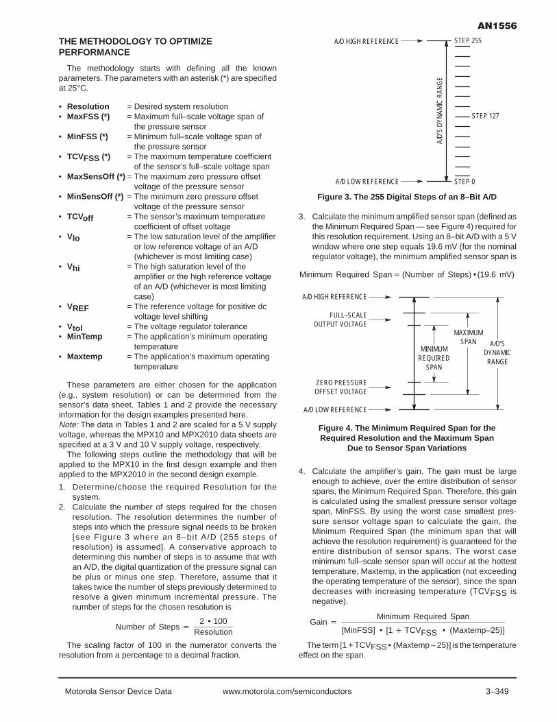
3–349Motorola Sensor Device Data www.motorola.com/semiconductors
THE METHODOLOGY TO OPTIMIZEPERFORMANCE
The methodology starts with defining all the knownparameters. The parameters with an asterisk (*) are specifiedat 25°C.
• Resolution• MaxFSS (*)
• MinFSS (*)
• TCVFSS (*)
• MaxSensOff (*)
• MinSensOff (*)
• TCVoff
• Vlo
• Vhi
• VREF
• Vtol• MinTemp
• Maxtemp
= Desired system resolution= Maximum full–scale voltage span of= the pressure sensor= Minimum full–scale voltage span of= the pressure sensor= The maximum temperature coefficient= of the sensor’s full–scale voltage span= The maximum zero pressure offset= voltage of the pressure sensor= The minimum zero pressure offset= voltage of the pressure sensor= The sensor’s maximum temperature= coefficient of offset voltage= The low saturation level of the amplifier= or low reference voltage of an A/D= (whichever is most limiting case)= The high saturation level of the= amplifier or the high reference voltage= of an A/D (whichever is most limiting= case)= The reference voltage for positive dc= voltage level shifting= The voltage regulator tolerance= The application’s minimum operating= temperature= The application’s maximum operating= temperature
These parameters are either chosen for the application(e.g., system resolution) or can be determined from thesensor’s data sheet. Tables 1 and 2 provide the necessaryinformation for the design examples presented here.Note: The data in Tables 1 and 2 are scaled for a 5 V supplyvoltage, whereas the MPX10 and MPX2010 data sheets arespecified at a 3 V and 10 V supply voltage, respectively.
The following steps outline the methodology that will beapplied to the MPX10 in the first design example and thenapplied to the MPX2010 in the second design example.
1. Determine/choose the required Resolution for thesystem.
2. Calculate the number of steps required for the chosenresolution. The resolution determines the number ofsteps into which the pressure signal needs to be broken[see Figure 3 where an 8–bit A/D (255 steps ofresolution) is assumed]. A conservative approach todetermining this number of steps is to assume that withan A/D, the digital quantization of the pressure signal canbe plus or minus one step. Therefore, assume that ittakes twice the number of steps previously determined toresolve a given minimum incremental pressure. Thenumber of steps for the chosen resolution is
Number of Steps2 ·100
Resolution
The scaling factor of 100 in the numerator converts theresolution from a percentage to a decimal fraction.
A/D HIGH REFERENCE
A/D LOW REFERENCE
STEP 255
STEP 0
STEP 127
A/D
’S D
YNAM
IC R
ANG
E
Figure 3. The 255 Digital Steps of an 8–Bit A/D
3. Calculate the minimum amplified sensor span (defined asthe Minimum Required Span — see Figure 4) required forthis resolution requirement. Using an 8–bit A/D with a 5 Vwindow where one step equals 19.6 mV (for the nominalregulator voltage), the minimum amplified sensor span is
Minimum Required Span (Number of Steps)·(19.6 mV)
A/D HIGH REFERENCE
A/D LOW REFERENCE
ZERO PRESSUREOFFSET VOLTAGE
FULL–SCALEOUTPUT VOLTAGE
MINIMUMREQUIRED
SPAN
MAXIMUMSPAN A/D’S
DYNAMICRANGE
Figure 4. The Minimum Required Span for theRequired Resolution and the Maximum Span
Due to Sensor Span Variations
4. Calculate the amplifier’s gain. The gain must be largeenough to achieve, over the entire distribution of sensorspans, the Minimum Required Span. Therefore, this gainis calculated using the smallest pressure sensor voltagespan, MinFSS. By using the worst case smallest pres-sure sensor voltage span to calculate the gain, theMinimum Required Span (the minimum span that willachieve the resolution requirement) is guaranteed for theentire distribution of sensor spans. The worst caseminimum full–scale sensor span will occur at the hottesttemperature, Maxtemp, in the application (not exceedingthe operating temperature of the sensor), since the spandecreases with increasing temperature (TCVFSS isnegative).
GainMinimum Required Span
[MinFSS] · [1 TCVFSS · (Maxtemp–25)]
The term [1 + TCVFSS • (Maxtemp – 25)] is the temperatureeffect on the span.

3–350 Motorola Sensor Device Datawww.motorola.com/semiconductors
Summarizing (through Step 4), the calculations are basedon a minimum desired resolution. The resolution requirementdetermines the number of steps or “pieces” into which thesignal must be broken. This number of steps or “pieces”multiplied by the number of millivolts per step equals aminimum voltage range which is defined as the MinimumRequired Span. Finally to ensure that this Minimum RequiredSpan is achieved over the entire distribution of sensor spans,the gain is calculated using the worst case smallest sensorspan.Note: The gain also will have variation due to resistortolerances in the amplifier circuit. To ensure that the systemvariation due to resistor tolerances is negligible whencompared to other sources of variation, the system should bedesigned using resistors with tolerances of 1% or better.
5. Calculate the worst case Maximum Span. The MaximumSpan is the largest possible span and is calculated usingthe maximum full–scale sensor voltage span, MaxFSS,and the Gain. The worst case maximum full–scale sensorspan occurs at the coldest temperature, MinTemp. Aftercalculating the Maximum Span, the remaining dynamicrange within the A/D’s window or saturation levels of theamplifier is the smallest number of “bits” (most limitingcase) available for headroom.
Maximum Span =[Gain] • [MaxFSS] • [1 + TCVFSS • (MinTemp – 25)]
The term [1 + TCVFSS • (MinTemp – 25)] is the temperatureeffect on the span.
The Maximum Span calculated from the above equation isdepicted in Figure 4.
6. Calculate the Calculated Headroom. The CalculatedHeadroom is a subset of the general term “headroom”because it reserves “bits” in the A/D’s dynamic range onlyfor the sources of variation from the sensor’s zero–pres-sure offset voltage. Headroom, in general, is reserved forall sources of variation: system components, resistortolerances (if significant), and the sensor. However, thelargest part of the “headroom” must be reserved for thedevice–to–device variations and temperature effects onthe sensor’s zero–pressure offset voltage. Therefore, thesources of variation from the other system componentsare subtracted immediately from the headroom so thatthe focus can be on the sensor–related variations (referto Figure 5 and the following equation for the CalculatedHeadroom). For these design examples, the supply is asingle, regulated 5 V ± 5% supply (the regulator ’stolerance is referred to as Vtol). An assumption for atypical rail–to–rail op–amp’s saturation levels (referred toas Vlo and Vhi) is 0.2 V above the low supply rail (ground)and 0.2 V below the high supply rail (5 V). Additionally,the worst case (smallest) supply voltage is 5 V – 5% or4.75 V.
Calculated Headroom 5 ·(1–Vtol100
) – 2
·Vlo – Maximum Span
The preceding equation assumes that the differencebetween Vhi and the high supply rail (or high reference of anA/D) is equal to the difference between Vlo and the low supplyrail (or low reference of an A/D); thus the term (2 • Vlo).
VS’s NOMINAL VALUE(NOT INCLUDING Vtol)
VS (INCLUDING Vtol) ANDA/D HIGH REFERENCE
HIGH SAT. LEVELOF AMPLIFIER
FULL–SCALEOUTPUT VOLTAGE
ZERO PRESSUREOFFSET VOLTAGE
LOW SAT. LEVELOF AMPLIFIER
GROUND AND A/DLOW REFERENCE
MAXIMUMSPAN
CALCULATEDHEADROOM
AMPLIFIER’SDYNAMICRANGE
Figure 5. From Ground to V S, a Section of Voltage IsReserved for Each Source of Variation
Step 6 is considered a pivotal step because it transitions themethodology’s calculations from the performance require-ments to the headroom requirements. Up to Step 6, themethodology considered only the span of the sensor toguarantee a minimum resolution despite device–to–devicevariation, component tolerances, and temperature effects.Upon calculating the Calculated Headroom, the remainingsteps of the methodology that are detailed below consider theoffset variations (due to device–to–device and temperature).These offset variations are added together to comprise whatis defined as the Required Headroom which is the requirednumber of “bits” in the A/D’s dynamic range needed toaccommodate the offset variations. This Required Headroomis then compared to the Calculated Headroom (from thepreceding calculation) to determine if the Calculated Head-room is sufficient to allow for the offset variations (i.e., theCalculated Headroom must be greater than or equal to theRequired Headroom). In the case that the Calculated Head-room is not sufficiently large, relaxing the resolution require-ment or reducing, if possible, the variation of either offset,span, component tolerances, or a combination of all three isrequired.
7. Calculate the maximum offset drift due to temperaturefluctuations (defined as the Maximum Temperature Effecton Offset). A conservative approach to this calculation isto determine the maximum total voltage change of offsetover the application’s entire operating temperature range.This maximum change of offset is the product of the Gain,TCVoff, and the application’s entire operating temperaturerange (from Maxtemp to MinTemp). Since the tempera-ture coefficient of offset can be positive or negative, theoffset may increase or decrease with increasing tempera-ture and, likewise, for decreasing temperature. Thoughthis step only considers the maximum magnitude of thechange in offset due to temperature, a segment in theRequired Headroom is reserved for both possibilities of apositive or negative temperature coefficient of offset (seeFigure 6). The sign (positive or negative) of the total offsetchange due to temperature is also considered in upcom-ing steps.

3–351Motorola Sensor Device Data www.motorola.com/semiconductors
Maximum Temperature Effect on Offset = (Gain) • (TCVoff) • (Maxtemp – MinTemp)
MAX. TEMPERATUREEFFECT ON OFFSET
(POSITIVE TEMP. COEFF.)
MAX. TEMPERATUREEFFECT ON OFFSET
(NEGATIVE TEMP. COEFF.)
REQUIREDHEADROOM
Figure 6. The Maximum Temperature Effect on Offset
8. Calculate the Maximum Offset Variation. The MaximumOffset Variation is the total amount of the RequiredHeadroom that must be reserved to account for the entiredistribution of sensor offsets (at room temperature —refer to Figure 7).
where largest offset is
and the smallest offset is
Maximum Offset Variation = [Gain] • [MaxSensOff – MinSensOff]
[Gain] • [MaxSensOff]
[Gain] • [MinSensOff]
9. Calculate the worst case Minimum Offset. The worst caseMinimum Offset includes both temperature effects (fromStep 7) and device–to–device variations (from Step 8) todetermine the smallest possible offset over the entiredistribution of sensor offsets and over the operatingtemperature range. This worst case Minimum Offsetoccurs when a sensor has a nominal room temperatureoffset of MinSensOff (smallest offset in the sensor offsetdistribution) and a negative temperature coefficient sothat the offset decreases with increasing temperature.Refer to Figure 7.
Minimum Offset = [Gain] •[MinSensOff] – Maximum Temperature Effect on Offset
10. Similar to Step 9, calculate the worst case MaximumOffset. The worst case Maximum Offset includes bothtemperature effects (from Step 7) and device–to–devicevariations (from Step 8) to determine the largest possibleoffset over the entire distribution of sensor offsets andover the operating temperature range. This worst caseMaximum Offset occurs when a sensor has a nominalroom temperature offset of MaxSensOff (largest offset inthe sensor offset distribution) and a positive temperaturecoefficient so that the offset increases with increasingtemperature. Refer to Figure 7.
Maximum Offset = [Gain] •[MaxSensOff] + Maximum Temperature Effect on Offset
MAXIMUMOFFSET
MINIMUMOFFSET
MAX. TEMPERATUREEFFECT ON OFFSET
(POSITIVE TEMP. COEFF.)
MAX. TEMPERATUREEFFECT ON OFFSET
(NEGATIVE TEMP. COEFF.)
REQUIREDHEADROOM
MAX. OFFSET VARIATION(BEFORE ADDINGTEMP. EFFECTS)
Figure 7. Calculating the Maximum andMinimum Offsets
11. Calculate the Required Headroom. Referring to Figure 7,the Required Headroom is the difference between theMaximum Offset and Minimum Offset and is the amountof voltage range (bits of the A/D) required to allow fordevice–to–device and temperature variations of thesensor’s offset.
Required Headroom = Maximum Offset – Minimum Offset
12. Compare the Required Headroom of Step 11 to theCalculated Headroom of Step 6. The Calculated Head-room is the absolute maximum amount of offset variation(due to device–to–device variations and temperatureeffects) that the system can allow for the desiredresolution. If the Required Headroom is greater than theCalculated Headroom, the desired resolution is notattainable for all worst case variations due to temperatureeffects, component tolerances, and device–to–devicevariations. Therefore, the requirement to attain thedesired system resolution is:
Calculated Headroom ≥ Required Headroom
If this requirement is not met, as stated previously, thealternatives to meeting this requirement are the following:
• Relax the Resolution requirement and repeat the meth-odology.
• Reduce (tighten) the span or offset (or both) variation andrepeat the methodology.
• Reduce temperature coefficients.• Reduce the component tolerances and repeat the
methodology.• Repeat the methodology by performing a combination of
the above suggestions.

3–352 Motorola Sensor Device Datawww.motorola.com/semiconductors
Once the above headroom requirement is met, the final stepis to determine the proper value of VREF:
13. A dc offset, VREF, is required to position the sensor’s spanwithin the A/D window so that no device–to–device ortemperature variation nor component tolerances causethe sensor’s output to be outside the A/D window.Therefore, calculate the VREF required to ensure that thesensor’s smallest zero–pressure offset voltage (MinimumOffset) is greater than or equal to Vlo (refer to Figures 5and 7). In other words, the sum of the reference voltageand Minimum Offset must be greater than or equal to theamplifier’s low saturation voltage:
VREF + Minimum Offset ≥ Vlo
Solving for VREF:
VREF ≥ Vlo – Minimum Offset
Note: The reference voltage, VREF, also will have variation dueto resistor tolerances in the resistor divider used to createVREF. To ensure that the system variation due to resistortolerances is negligible when compared to other sources ofvariation, the system should be designed using resistors withtolerances of 1% or better.
The following design examples use the methodology.
DESIGN EXAMPLES WITH THE MPX10 ANDMPX2010
The following table lists the methodology’s steps. The tableentries (names) will correspond to the names used in themethodology outlined above; additionally, the step number(Step 1, etc.) is bracketed ( [ ] ) and superscripted next to theentry to which the step refers. The first column lists the givenparameters that should be available in or derived from theappropriate component’s (sensor, amplifier, voltage regulator,resistors) data sheet. The second column lists theperformance requirements of the sensor system (i.e., thiscolumn lists all the calculations that relate to ensuring aminimum sensor span to achieve the desired resolutiondespite device–to–device variations, temperature effects andcomponent tolerances). The third column lists the calculationsthat determine the headroom for the system given componenttolerances and the device–to–device variations andtemperature effects on the sensor’s offset. The table andassociated system design equations may easily beimplemented in a spreadsheet to efficiently perform therequired calculations.
Table 3. Design Example Using the MPX10
Given Parameters Performance Parameters Headroom Parameters
MaxFSS(mV @ 25°C)
83
[1]Resolution (% FSS)4.5
[7]Maximum Temperature Effect on Offset(V)
0.03
MinFSS(mV @ 25°C)
33
[2]Number of Steps44
[8]Maximum Offset Variation(V)
1.76
TCVFSS(% FSS/°C)
–0.22
[3]Minimum Required Span(V)
0.87
[9]Minimum Offset(V)
–0.03
MaxSensOff(mV @ 25°C)
58
[4]Gain29
[10]Maximum Offset(V)
1.73
MinSensOff(mV @ 25°C)
0
[5]Maximum Span(V)
2.57
[13]VREF(V)
0.23
TCVoff(µV/°C)
±15
VS(V)5
[6]Calculated Headroom(V)
1.78
[11]Required Headroom(V)
1.75
Vhi(V)4.8
Vlo(V)0.2
[12]ISCalculated Headroom ≥Required Headroom ?
Vtol(%)5
Maxtemp(°C)70
MinTemp(°C)
0

3–353Motorola Sensor Device Data www.motorola.com/semiconductors
Table 4. Design Example Using the MPX2010
Given Parameters Performance Parameters Headroom Parameters
MaxFSS(mV @ 25°C)
13
[1]Resolution (% FSS)1.2
[7]Maximum Temperature Effect on Offset(V)
0.14
MinFSS(mV @ 25°C)
12
[2]Number of Steps167
[8]Maximum Offset Variation(V)
0.55
TCVFSS(% FSS)
±1
[3]Minimum Required Span(V)
3.27
[9]Minimum Offset(V)
–0.27
MaxSensOff(mV @ 25°C)
0.5
[4]Gain275
[10]Maximum Offset(V)
0.27
MinSensOff(mV @ 25°C)
–0.5
[5]Maximum Span(V)
3.61
[13]VREF(V)
0.47
TCVoff(mV, 0°C to 85°C)
±0.5
VS(V)5
[6]Calculated Headroom(V)
0.74
[11]Required Headroom(V)
0.55
Vhi(V)4.8
Vlo(V)0.2
[12]ISCalculated Headroom ≥Required Headroom ?
Vtol(%)5
Maxtemp(°C)85
MinTemp(°C)
0

3–354 Motorola Sensor Device Datawww.motorola.com/semiconductors
DESIGN EXAMPLE COMPARISON SUMMARY
The preceding examples show how sources of variation canaffect the overall system resolution. The MPX2010 hason–chip temperature compensation and calibration circuitry toreduce device–to–device variations and temperature effects.Consequently, when designing the fixed–value amplifiercircuitry, the resolution possible with the MPX2010 is almostfour times greater than the same amplifier circuit using anMPX10. In both examples, both systems’ performance(Resolution) are optimized to be the best possible, given thedistribution of the sensor device parameters and the othercomponent variations.
As stated previously if the methodology’s calculations showthat the sensor’s signal will always be within the dynamicrange of the amplifier (and high and low reference voltages ofthe A/D), a software calibration may then be implemented tonullify any room temperature device–to–device andcomponent variations.
It should be noted, however, that this methodology does notconsider how to obtain the best performance from a singlesensor system. Rather, the focus of the methodology is toobtain the best possible system performance whileconsidering the distribution of device parameters that resultfrom manufacturing and other sources of variation. Byconsidering the sources of variation, the system may then bemass–produced without individually calibrating the sensorsystem hardware. Obviously, if each sensor system ishand–calibrated, the performance will be better. However, thehand–calibration also requires additional cost and time whenproducing the sensor system.
CONCLUSION
To guarantee a specified performance when designing afixed–value circuit for sensor systems, all significant sourcesof variation must be considered. By considering the sourcesof variation (device–to–device variations, temperature effects,and component tolerances), the system may be designed sothat the specified performance (resolution) is achieved whilestill keeping the sensor’s amplified dynamic range within theA/D window (or saturation levels of the amplifier). Thespecified performance may be achieved in all cases byapplying the methodology described herein. By first calculat-ing the Minimum Required Span to achieve the requiredresolution in all scenarios and then determining if theremaining dynamic range or headroom is large enough toaccommodate the sources of variation, the methodologydetermines if the resolution requirement is feasible. If thesources of variation are too large, the resolution requirementmay not be attainable. In such a case, the resolutionrequirement should be relaxed, or the sources of variationmust be decreased. Finally, once the system is successfullydesigned to ensure that the sensor signal will always be withinthe dynamic range of the amplifier (and high and low referencevoltages of the A/D), a software calibration may be implement-ed to nullify any room temperature device–to–device andcomponent variations.

3–355Motorola Sensor Device Data www.motorola.com/semiconductors
Prepared by: C.S. Chua and Siew Mun HinSensor Application EngineeringSingapore, A/P
INTRODUCTION
This application note describes a Digital Blood PressureMeter concept which uses an integrated pressure sensor,analog signal–conditioning circuitry, microcontrollerhardware/software and a liquid crystal display. The sensingsystem reads the cuff pressure (CP) and extracts the pulsesfor analysis and determination of systolic and diastolicpressure. This design uses a 50 kPa integrated pressuresensor (Motorola P/N: MPXV5050GP) yielding a pressurerange of 0 mmHg to 300 mmHg.
CONCEPT OF OSCILLOMETRIC METHOD
This method is employed by the majority of automatednon–invasive devices. A limb and its vasculature arecompressed by an encircling, inflatable compression cuff. Theblood pressure reading for systolic and diastolic bloodpressure values are read at the parameter identification point.
The simplified measurement principle of the oscillometricmethod is a measurement of the amplitude of pressurechange in the cuff as the cuff is inflated from above the systolicpressure. The amplitude suddenly grows larger as the pulsebreaks through the occlusion. This is very close to systolicpressure. As the cuff pressure is further reduced, the pulsationincrease in amplitude, reaches a maximum and thendiminishes rapidly. The index of diastolic pressure is takenwhere this rapid transition begins. Therefore, the systolic
blood pressure (SBP) and diastolic blood pressure (DBP) areobtained by identifying the region where there is a rapidincrease then decrease in the amplitude of the pulsesrespectively. Mean arterial pressure (MAP) is located at thepoint of maximum oscillation.
HARDWARE DESCRIPTION AND OPERATION
The cuff pressure is sensed by Motorola’s integratedpressure X–ducer . The output of the sensor is split into twopaths for two different purposes. One is used as the cuffpressure while the other is further processed by a circuit.Since MPXV5050GP is signal–conditioned by its internalop–amp, the cuff pressure can be directly interfaced with ananalog–to–digital (A/D) converter for digitization. The otherpath will filter and amplify the raw CP signal to extract anamplified version of the CP oscillations, which are caused bythe expansion of the subject’s arm each time pressure in thearm increases during cardiac systole.
The output of the sensor consists of two signals; theoscillation signal ( ≈ 1 Hz) riding on the CP signal ( ≤ 0.04 Hz).Hence, a 2–pole high pass filter is designed to block the CPsignal before the amplification of the oscillation signal. If theCP signal is not properly attenuated, the baseline of theoscillation will not be constant and the amplitude of eachoscillation will not have the same reference for comparison.Figure 1 shows the oscillation signal amplifier together withthe filter.
Figure 1. Oscillation Signal Amplifier
C2
+5V
R2
–
+
+DC offset
U1a
3
21
150k
LM324N0.33u
Vi
R3 1M 11
4
Vo
R1
1k
C1
33u
SEMICONDUCTOR APPLICATION NOTE

3–356 Motorola Sensor Device Datawww.motorola.com/semiconductors
The filter consists of two RC networks which determine twocut–off frequencies. These two poles are carefully chosen toensure that the oscillation signal is not distorted or lost. The
two cut–off frequencies can be approximated by the followingequations. Figure 2 describes the frequency response of thefilter. This plot does not include the gain of the amplifier.
10
0
–10
–20
–30
–40
–50
–60
–70
–8010 10010.10.01
Frequency (Hz)
Figure 2. Filter Frequency Response
Oscillation Signal (1 Hz)
CP Signal (0.04 Hz)
Atte
nuat
ion
(dB)
fP1 =1
2R1C1
fP2 =1
2R3C2

3–357Motorola Sensor Device Data www.motorola.com/semiconductors
The oscillation signal varies from person to person. Ingeneral, it varies from less than 1 mmHg to 3 mmHg. From thetransfer function of MPXV5050GP, this will translate to avoltage output of 12 mV to 36 mV signal. Since the filter givesan attenuation of 10 dB to the 1 Hz signal, the oscillation signalbecomes 3.8 mV to 11.4 mV respectively. Experiments
indicate that, the amplification factor of the amplifier is chosento be 150 so that the amplified oscillation signal is within theoutput limit of the amplifier (5 mV to 3.5 V). Figure 3(a) showsthe output from the pressure sensor and Figure 3(b) shows theextracted oscillation signal at the output of the amplifier.
Figure 3. CP signal at the output of the pressure sensor
Oscillation signal is extracted here
3
2.5
2
1.5
1
0.5
00 5 10 15 20 25 30 35 40
Time (seconds)
Vi (
volts
)
3
2.5
2
1.5
1
0.5
0
Vo
(vol
ts)
10 15 20 25 30 35
Time (seconds)
MAP
DBPSBP
3.5
Figure 3b. Extracted oscillation signal at the output of amplifier

3–358 Motorola Sensor Device Datawww.motorola.com/semiconductors
Referring to the schematic, Figure 4, the MPX5050GPpressure sensor is connected to PORT D bit 5 and the outputof the amplifier is connected to PORT D bit 6 of themicrocontroller. This port is an input to the on–chip 8–bitanalog–to–digital (A/D) converter. The pressure sensorprovides a signal output to the microprocessor ofapproximately 0.2 Vdc at 0 mmHg to 4.7 Vdc at 375 mmHg ofapplied pressure whereas the amplifier provides a signal from0.005 V to 3.5 V. In order to maximize the resolution, separatevoltage references should be provided for the A/D instead ofusing the 5 V supply. In this example, the input range of the A/Dconverter is set at approximately 0 Vdc to 3.8 Vdc. Thiscompresses the range of the A/D converter around 0 mmHgto 300 mmHg to maximize the resolution; 0 to 255 counts is therange of the A/D converter. VRH and VRL are the referencevoltage inputs to the A/D converter. The resolution is definedby the following:
Count = [(VXdcr – VRL)/(VRH – VRL)] x 255
The count at 0 mmHg = [(0.2 – 0)/(3.8 – 0)] x 255 ≈ 14The count at 300 mmHg = [(3.8 – 0)/(3.8 – 0)] x 255 ≈ 255Therefore the resolution = 255 – 14 = 241 counts. This
translates to a system that will resolve to 1.24 mmHg.The voltage divider consisting of R5 and R6 is connected to
the +5 volts powering the system. The output of the pressuresensor is ratiometric to the voltage applied to it. The pressuresensor and the voltage divider are connected to a commonsupply; this yields a system that is ratiometric. By nature of this
ratiometric system, variations in the voltage of the powersupplied to the system will have no effect on the systemaccuracy.
The liquid crystal display (LCD) is directly driven from I/Oports A, B, and C on the microcontroller. The operation of aLCD requires that the data and backplane (BP) pins must bedriven by an alternating signal. This function is provided by asoftware routine that toggles the data and backplane atapproximately a 30 Hz rate.
Other than the LCD, there are two more I/O devices that areconnected to the pulse length converter (PLM) of themicrocontroller; a buzzer and a light emitting diode (LED). Thebuzzer, which connected to the PLMA, can produce twodifferent frequencies; 122 Hz and 1.953 kHz tones. Forinstance when the microcontroller encounters certain errordue to improper inflation of cuff, a low frequency tone is alarm.In those instance when the measurement is successful, a highfrequency pulsation tone will be heard. Hence, differentmusical tone can be produced to differential each condition. Inaddition, the LED is used to indicate the presence of a heartbeat during the measurement.
The microcontroller section of the system requires certainsupport hardware to allow it to function. The MC34064P–5provides an undervoltage sense function which is used toreset the microprocessor at system power–up. The 4 MHzcrystal provides the external portion of the oscillator functionfor clocking the microcontroller and provides a stable base fortime based functions, for instance calculation of pulse rate.
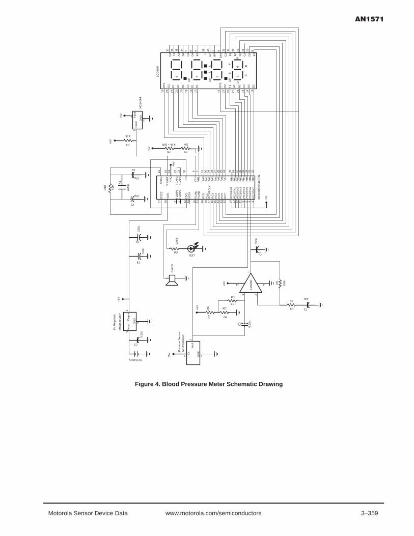
3–359Motorola Sensor Device Data www.motorola.com/semiconductors
Figure 4. Blood Pressure Meter Schematic Drawing
PC
0P
C1
PC
2/E
CLK
PC
3P
C4
PC
5P
C6
PC
7
PD
0/A
N0
+5V
+5V
+5V
+5V
+5V
+5V
+5V
+5V
Pre
ssur
e S
enso
rM
PX
V50
50G
P
Vou
t
GN
D
2
3
Vs
9V Battery
C51
1
2
GN
D
0.33
u
Inpu
tO
utpu
t
5V R
egul
ator
MC
78L0
5AC
P
Buz
zer
0.33
u
C2
3
1
3 2
R4 R0
10k
24k
R3
1M
11LM
324N 4
R1 C1
1k33u
150kR2
C7LED
R8
100R
100n
100u
C8
C6
330u
R10
10M
X1
4MH
z
C3
C4
22p
22p
PD
1/A
N1
PD
2/A
N2
PD
3/A
N3
PD
4/A
N4
PD
5/A
N5
PD
6/A
N6
PD
7/A
N7
PLM
BP
LMA
SC
LKT
DO
TC
MP
2T
CM
P1
VD
D
OS
C2
MC
68H
C05
B16
CF
N
OS
C1
/RE
SE
T/IR
Q
TC
AP
1T
CA
P2
RD
VR
HV
RL
PA
0P
A1
PA
2P
A3
PA
4P
A5
PA
6P
A7
PB
0P
B1
PB
2P
B3
PB
4P
B5
PB
6P
B7
R6R5
4.7k + 36R 15kR9
4.7k
+5V
MC
3406
4
Res
etIn
put
GN
D
LCD
5657
1
32
17 10 2 1 52 51 20 21 49 48 47 46 45 44 43 42 14 13 12 11 9 5 4 33233343536373839242526272829303178502322191816
16 23 22 21 20 19 18 17 12 27 26 25 24 15 14 13
CB
AG
1DD
PE
F
2
DP
LL
3
DP
4
DP
1
G1
F1
A1
B1
C1
D1
E1
DP
2
G2
F2
A2
B2
C2
D2
E2
37 36 35 34 7 6 5 28 40 1 8 32 31 30 29 11 10 9
G4
F4
A4
B4
C4
D4
E4 L
BP
BP
DP
3
G3
F3
A3
B3
C3
D3
E3

3–360 Motorola Sensor Device Datawww.motorola.com/semiconductors
SOFTWARE DESCRIPTIONUpon system power–up, the user needs to manually pump
the cuff pressure to approximately 160 mmHg or 30 mmHgabove the previous SBP. During the pumping of the inflationbulb, the microcontroller ignores the signal at the output of the
amplifier. When the subroutine TAKE senses a decrease inCP for a continuous duration of more than 0.75 seconds, themicrocontroller will then assume that the user is no longerpumping the bulb and starts to analyze the oscillation signal.Figure 5 shows zoom–in view of a pulse.
–7.1–7.3–7.5–7.7–7.9–8.1–8.3–8.5
Time (second)
Figure 5. Zoom–in view of a pulse
Vo (v
olt)
450 ms
Premature pulse
1.75
First of all, the threshold level of a valid pulse is set to be 1.75V to eliminate noise or spike. As soon as the amplitude of apulse is identified, the microcontroller will ignore the signal for450 ms to prevent any false identification due to the presenceof premature pulse ”overshoot” due to oscillation. Hence, thisalgorithm can only detect pulse rate which is less than 133beats per minute. Next, the amplitudes of all the pulsesdetected are stored in the RAM for further analysis. If themicrocontroller senses a non–typical oscillation envelope
shape, an error message (“Err”) is output to the LCD. The userwill have to exhaust all the pressure in the cuff beforere–pumping the CP to the next higher value. The algorithmensures that the user exhausts all the air present in the cuffbefore allowing any re–pumping. Otherwise, the venous bloodtrapped in the distal arm may affect the next measurement.Therefore, the user has to reduce the pressure in the cuff assoon as possible in order for the arm to recover. Figure 6 is aflowchart for the program that controls the system.
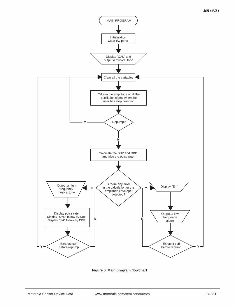
3–361Motorola Sensor Device Data www.motorola.com/semiconductors
Figure 6. Main program flowchart
MAIN PROGRAM
InitializationClear I/O ports
Display ”CAL” andoutput a musical tone
Clear all the variables
Take in the amplitude of all theoscillation signal when the
user has stop pumping
Calculate the SBP and DBPand also the pulse rate
Repump?
Is there any errorin the calculation or the
amplitude envelopedetected?
Output a highfrequency
musical tone
Exhaust cuffbefore repump
Exhaust cuffbefore repump
Display pulse rate.Display ”SYS” follow by SBP.Display ”dlA” follow by DBP.
Display ”Err”
Output a lowfrequency
alarm
N
N
N N
Y
Y
Y Y

3–362 Motorola Sensor Device Datawww.motorola.com/semiconductors
SELECTION OF MICROCONTROLLERAlthough the microcontroller used in this project is
MC68HC05B16, a smaller ROM version microcontroller canalso be used. The table below shows the requirement ofmicrocontroller for this blood pressure meter design in thisproject.
Table 1. Selection of microcontroller
ÁÁÁÁÁÁÁÁÁÁÁÁÁÁÁÁÁÁÁÁÁÁÁÁÁÁÁÁÁÁÁÁÁÁ
On–chip ROM space 2 kilobytesÁÁÁÁÁÁÁÁÁÁÁÁÁÁÁÁÁÁÁÁÁÁÁÁÁÁÁÁÁÁÁÁÁÁ
On–chip RAM space 150 bytesÁÁÁÁÁÁÁÁÁÁÁÁÁÁÁÁÁÁÁÁÁÁÁÁÁÁÁÁÁÁÁÁÁÁ2–channel A/D converter (min.)ÁÁÁÁÁÁÁÁÁÁÁÁÁÁÁÁÁÁÁÁÁÁÁÁÁÁÁÁÁÁÁÁÁÁ16–bit free running counter timerÁÁÁÁÁÁÁÁÁÁÁÁÁÁÁÁÁÁÁÁÁÁÁÁÁÁÁÁÁÁÁÁÁÁÁÁÁÁÁÁÁÁÁÁÁÁÁÁÁÁÁ
LCD driver
ÁÁÁÁÁÁÁÁÁÁÁÁÁÁÁÁÁÁÁÁÁÁÁÁÁÁÁÁÁÁÁÁÁÁ
On–chip EEPROM space 32 bytes
ÁÁÁÁÁÁÁÁÁÁÁÁÁÁÁÁÁÁÁÁÁÁÁÁÁÁÁÁÁÁÁÁÁÁ
Power saving Stop and Wait modes
CONCLUSION
This circuit design concept may be used to evaluateMotorola pressure sensors used in the digital blood pressuremeter. This basic circuit may be easily modified to providesuitable output signal level. The software may also be easilymodified to provide better analysis of the SBP and DBP of aperson.
REFERENCES
Lucas, Bill (1991). “An Evaluation System for Direct Interfaceof the MPX5100 Pressure Sensor with a Microprocessor,”Motorola Application Note AN1305.

3–363Motorola Sensor Device Data www.motorola.com/semiconductors
Prepared by: David HeeleySystems and Applications EngineeringMotorola Semiconductor Products SectorSensor Products DivisionPhoenix, Arizona
Introduction
Fluid systems, pressure and pressure measurements are extremely complex. The typical college curriculum for MechanicalEngineers includes at least two semesters in fluid mechanics. This paper will define and explain the basic concepts of fluidmechanics in terms that are easily understood while maintaining the necessary technical accuracy and level of detail.
Pressure and Pressure Measurement
What is fluid pressure? Fluid pressure can be defined as the measure of force per–unit–area exerted by a fluid, actingperpendicularly to any surface it contacts (a fluid can be either a gas or a liquid, fluid and liquid are not synonymous). The standardSI unit for pressure measurement is the Pascal (Pa) which is equivalent to one Newton per square meter (N/m2) or the KiloPascal(kPa) where 1 kPa = 1000 Pa. In the English system, pressure is usually expressed in pounds per square inch (psi). Pressure canbe expressed in many different units including in terms of a height of a column of liquid. The table below lists commonly used unitsof pressure measurement and the conversion between the units.
kPa mm Hg millibar in H2O PSI
1 atm 101.325 760.000 1013.25 406.795 14.6960
1 kPa 1.000 7.50062 10.000 4.01475 0.145038
1 mm Hg 0.133322 1.000 1.33322 0.535257 0.0193368
1 millibar 0.1000 0.750062 1.000 0.401475 0.0145038
1 in H2O 0.249081 1.86826 2.49081 1.000 0.0361
1 PSI 6.89473 51.7148 68.9473 27.6807 1.000
1 mm H2O 0.009806 0.07355 9.8 x 10⁻⁸ 0.03937 0.0014223
Figure 1. Conversion Table for Common Units of Pressure
Pressure measurements can be divided into three different categories: absolute pressure, gage pressure and differentialpressure. Absolute pressure refers to the absolute value of the force per–unit–area exerted on a surface by a fluid. Therefore theabsolute pressure is the difference between the pressure at a given point in a fluid and the absolute zero of pressure or a perfectvacuum. Gage pressure is the measurement of the difference between the absolute pressure and the local atmospheric pressure.Local atmospheric pressure can vary depending on ambient temperature, altitude and local weather conditions. The U.S. standardatmospheric pressure at sea level and 59°F (20°C) is 14.696 pounds per square inch absolute (psia) or 101.325 kPa absolute(abs). When referring to pressure measurement, it is critical to specify what reference the pressure is related to. In the Englishsystem of units, measurement relating the pressure to a reference is accomplished by specifying pressure in terms of pounds persquare inch absolute (psia) or pounds per square inch gage (psig). For other units of measure it is important to specify gage orabsolute. The abbreviation ‘abs’ refers to an absolute measurement. A gage pressure by convention is always positive. A ‘negative’gage pressure is defined as vacuum. Vacuum is the measurement of the amount by which the local atmospheric pressure exceedsthe absolute pressure. A perfect vacuum is zero absolute pressure. Figure 2 shows the relationship between absolute, gagepressure and vacuum. Differential pressure is simply the measurement of one unknown pressure with reference to anotherunknown pressure. The pressure measured is the difference between the two unknown pressures. This type of pressuremeasurement is commonly used to measure the pressure drop in a fluid system. Since a differential pressure is a measure of onepressure referenced to another, it is not necessary to specify a pressure reference. For the English system of units this could simplybe psi and for the SI system it could be kPa.
SEMICONDUCTOR APPLICATION NOTE

3–364 Motorola Sensor Device Datawww.motorola.com/semiconductors
Pressure
Local Atmospheric Pressure
Vacuum (Negative Gage)
Absolute
Absolute
Atmospheric
Gage
Figure 2. Pressure Term Relationships
In addition to the three types of pressure measurement, there are different types of fluid systems and fluid pressures. There aretwo types of fluid systems; static systems and dynamic systems. As the names imply, a static system is one in which the fluid isat rest and a dynamic system is on in which the fluid is moving.
Static Pressure Systems
The pressure measured in a static system is static pressure. In the pressure system shown in Figure 3, a uniform static fluidis continuously distributed with the pressure varying only with vertical distance. The pressure is the same at all points along thesame horizontal plane in the fluid and is independent of the shape of the container. The pressure increases with depth in the fluidand acts equally in all directions. The increase in pressure at a deeper depth is essentially the effect of the weight of the fluid abovethat depth. Figure 4 shows two containers with the same fluid exposed to the same external pressure – P . At any equal depth withineither tank the pressure will be the same . Note that the sides of the large tank are not vertical. The pressure is dependent onlyon depth and has nothing to do with the shape of the container. If the working fluid is a gas, the pressure increase in the fluid dueto the height of the fluid is in most cases negligible since the density and therefore the weight of the fluid is much smaller than thepressure being applied to the system. However, this may not remain true if the system is large enough or the pressures low enough.One example considers how atmospheric pressure changes with altitude. At sea level the standard U.S. atmospheric pressureis 14.696 psia (101.325 kPa). At an altitude of 10,000 ft (3048 m) above sea level the standard U.S. atmospheric pressure is 10.106psia (69.698 kPA) and at 30,000 ft (9144 m), the standard U.S. atmospheric pressure is 4.365 psia (30.101 kPa).
The pressure in a static liquid can be easily calculated if the density of the liquid is known. The absolute pressure at a depth Hin a liquid is defined as:
Pabs = P + (ρ x g x H)
Where :Pabs is the absolute pressure at depth H.P is the external pressure at the top of the liquid. For most open systems this will be atmospheric pressure.ρ is the density of the fluid.g is the acceleration due to gravity (g = 32.174 ft/sec2 (9.81 m/sec2)).H is the depth at which the pressure is desired.

3–365Motorola Sensor Device Data www.motorola.com/semiconductors
ÎÎÎÎÎÎÎÎÎÎÎÎÎÎÎÎÎÎÎÎÎÎÎÎÎÎÎÎÎÎÎÎÎÎÎÎÎÎÎÎÎÎÎÎÎÎÎÎÎÎÎÎÎÎÎÎÎÎÎÎÎÎÎÎÎÎÎÎÎÎÎÎÎÎÎÎÎÎÎÎÎÎÎÎÎÎÎÎÎÎÎÎÎÎÎÎÎÎÎÎÎÎÎÎÎÎÎÎÎÎÎÎÎÎÎÎÎÎÎÎÎÎÎÎÎÎÎÎÎÎÎÎÎÎÎÎÎÎÎÎÎÎÎÎÎÎÎÎÎÎÎÎÎÎÎÎÎÎÎÎÎÎÎÎÎÎÎÎ
ÎÎÎÎÎÎÎÎÎÎÎÎÎÎÎÎÎÎÎÎÎÎÎÎÎÎÎÎÎÎÎÎÎÎÎÎÎÎÎÎÎÎÎÎÎÎÎÎÎÎÎÎÎÎÎÎÎÎÎÎÎÎÎÎÎÎÎÎÎÎÎÎÎÎÎÎÎÎÎÎÎÎÎÎÎÎÎÎÎÎÎÎÎÎÎÎÎÎÎÎÎÎÎÎÎ
ÎÎÎÎÎÎÎÎÎÎÎÎÎÎÎÎÎÎÎÎÎ
Figure 3. Continuous Fluid System
Figure 4. Pressure Measurement at a Depth in a Liquid
Dynamic Pressure Systems
Dynamic pressure systems are more complex than static systems and can be more difficult to measure. In a dynamic system,pressure typically is defined using three different terms. The first pressure we can measure is static pressure. This pressure is thesame as the static pressure that is measured in a static system. Static pressure is independent of the fluid movement or flow. Aswith a static system the static pressure acts equally in all directions. The second type of pressure is what is referred to as thedynamic pressure. This pressure term is associated with the velocity or the flow of the fluid. The third pressure is total pressureand is simply the static pressure plus the dynamic pressure.
Steady–State Dynamic Systems
Care must be taken when measuring dynamic system pressures. For a dynamic system, under steady–state conditions,accurate static pressures may be measured by tapping into the fluid stream perpendicular to the fluid flow. For a dynamic system,steady–state conditions are defined as no change in the system flow conditions: pressure, flow rate, etc. Figure 5 illustrates adynamic system with a fluid flowing through a pipe or duct. In this example a static pressure tap is located in the duct wall at pointA. The tube inserted into the flow is called a Pitot tube. The Pitot tube measures the total pressure at point B in the system. Thetotal pressure measured at this point is referred to as the stagnation pressure. The stagnation pressure is the value obtained whena flowing fluid is decelerated to zero velocity in an isentropic (frictionless) process. This process converts all of the energy fromthe flowing fluid into a pressure that can be measured. The stagnation or total pressure is the static pressure plus the dynamicpressure. It is very difficult to accurately measure dynamic pressures. When dynamic pressure measurement is desired, the totaland static pressures are measured and then subtracted to obtain the dynamic pressure. Dynamic pressures can be used todetermine the fluid velocities and flow rates in dynamic systems.
When measuring dynamic system pressures, care must be taken to ensure accuracy. For static pressure measurements, thepressure tap location should be chosen so that the measurement is not influenced by the fluid flow. Typically, taps are locatedperpendicular to the flow field. In Figure 5, the static pressure tap at point A is in the wall of the duct and perpendicular to the flowfield. In Figures 6a and 6c the static taps (point A) in the pressure probes are also perpendicular to the flow field. These examplesshow the most common type of static pressure taps, however there are many different static pressure tap options. For total orstagnation pressure measurements, it is important that the Pitot or impact tube be aligned parallel to the flow field with the tipof the tube pointing directly into the flow. In Figures 6b and 6c, the Pitot tube is aligned parallel with the flow, with the tube openingpointing directly into the flow. Although the static pressure is independent of direction, the dynamic pressure is a vector quantitywhich depends on both magnitude and direction for the total measured value. If the Pitot tube is misaligned with the flow, accuracyof the total pressure measurement may suffer. In addition, for accurate pressure measurements the pressure tap holes and probesmust be smooth and free from any burrs or obstructions that could cause disturbances in the flow. The location of the pressuretaps and probes, static and total, must also be selected carefully. Any location in the system where the flow field may be disturbed
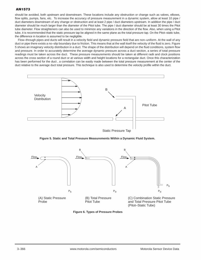
3–366 Motorola Sensor Device Datawww.motorola.com/semiconductors
should be avoided, both upstream and downstream. These locations include any obstruction or change such as valves, elbows,flow splits, pumps, fans, etc. To increase the accuracy of pressure measurement in a dynamic system, allow at least 10 pipe /duct diameters downstream of any change or obstruction and at least 2 pipe / duct diameters upstream. In addition the pipe / ductdiameter should be much larger than the diameter of the Pitot tube. The pipe / duct diameter should be at least 30 times the Pitottube diameter. Flow straighteners can also be used to minimize any variations in the direction of the flow. Also, when using a Pitottube, it is recommended that the static pressure tap be aligned in the same plane as the total pressure tap. On the Pitot–static tube,the difference in location is assumed to be negligible.
Flow–through pipes and ducts will result in a velocity field and dynamic pressure field that are non–uniform. At the wall of anyduct or pipe there exists a no–slip boundary due to friction. This means that at the wall itself the velocity of the fluid is zero. Figure5 shows an imaginary velocity distribution in a duct. The shape of the distribution will depend on the fluid conditions, system flowand pressure. In order to accurately determine the average dynamic pressure across a duct section, a series of total pressurereadings must be taken across the duct. These pressure measurements should be taken at different radii and clock positionsacross the cross section of a round duct or at various width and height locations for a rectangular duct. Once this characterizationhas been performed for the duct , a correlation can be easily made between the total pressure measurement at the center of theduct relative to the average duct total pressure. This technique is also used to determine the velocity profile within the duct.
VelocityDistribution
Static Pressure Tap
Pitot Tube
B
A
(A) Static PressureProbe
(B) Total PressurePitot Tube
(C) Combination Static Pressureand Total Pressure Pitot Tube(Pitot–Static Tube)
Flow Flow Flow
B B
AA
Ps
Ps
PoPo
Figure 5. Static and Total Pressure Measurements Within a Dynamic Fluid System.
Figure 6. Types of Pressure Probes

3–367Motorola Sensor Device Data www.motorola.com/semiconductors
Transient Systems
Transient systems are systems with changing conditions such as pressures, flow rates, etc. Measurements in transient systemsare the most difficult to accurately obtain. If the measurement system being used to measure the pressure has a faster responsetime than the rate of change in the system, then the system can be treated as quasi–steady–state. That is, the measurements willbe about as accurate as those taken in the steady–state system. If the measurement of the system is assumed to be a snap shotof what is happening in the system, then you want to be able to take the picture faster than the rate of change in the system orthe picture will be blurred. In other words, the measurement results will not be accurate. In a pressure measurement system, thereare two factors that determine the overall measurement response: (1) the response of the transducer element that senses thepressure, and (2) the response of the interface between the transducer and the pressure system such as the pressure transmittingfluid and the connecting tube, etc. For Motorola pressure sensors, the second factor usually determines the overall frequencyresponse of the pressure measurement system. The vast majority of pressure systems that require measurements today arequasi–steady–state systems where system conditions are changing relatively slowly compared to the response rate of themeasurement system or the change happens instantaneously and then stabilizes.
Two transient system examples include washing machines and ventilation ducts in buildings. In a washing machine, the heightof the water in the tub is measured indirectly by measuring the pressure at the bottom of the tub. As the tub fills the pressurechanges. The rate at which the tub fills and the pressure changes is much slower than the response rate of the measurementsystem. In a ventilation duct, the pressure changes as the duct registers are opened and closed, adjusting the air movement withinthe building. As more registers are opened and closed, the system pressure changes. The pressure changes are virtuallyinstantaneous. In this case, pressure changes are essentially incremental and therefore easy to measure accurately except at theinstant of the change. For most industrial and building control applications, the lag in the pressure measurement system isnegligible. As the control or measurement system becomes more precise, the frequency response of the measurement systemmust be considered.
Motorola Pressure Sensors
This application note has covered various types of pressures that are measured and how to tap into a system to measure thedesired pressures. How are the actual pressure measurements made? There are many types of pressure measurement systemsranging from simple liquid tube manometers to bourdon–tube type gages to piezo–electric silicon based transducers. Today, aselectronic control and measurement systems are replacing mechanical systems, silicon–based pressure transducers and sensorsare becoming the sensors of choice. Silicon micromachined sensors offer very high accuracies at very low cost and provide aninterface between the mechanical world and the electrical system. Motorola carries a complete line of silicon based pressuresensors which feature a wide range of pressures with various levels of integration on a single chip. These levels of integration startwith the basic uncompensated, uncalibrated pressure sensor all the way to the fully integrated, temperature compensated,calibrated and signal conditioned pressure sensors. The response time of Motorola’s MPX series silicon pressure sensors istypically 1 millisecond or less. For static or dynamic systems, Motorola’s pressure sensors are an excellent solution for pressuremeasurement systems.
Conclusion
Pressures and pressure measurements can be extremely complex and complicated. However, for most systems it is relativelyeasy to obtain accurate pressure measurements if the proper techniques are used.

3–368 Motorola Sensor Device Datawww.motorola.com/semiconductors
by: Eric JacobsenSystems and Applications EngineerSensor Products DivisionMotorola, Inc.
A digital output is more desirable than an analog output innoisy environments (e.g. automotive, washing machines,etc.) and remote sensing applications (building controls,industrial applications, etc.) because a digital signal inherentlyhas better noise immunity compared to analog signals.Additional applications requiring a sensor with a digital outputinclude microcontroller–based systems that have no A/D inthe system or that have no A/D channels available for thesensing function. For these applications, there is no otheroption but a digital output to further process the signal.
Via a design example this paper shows how to easilyconvert an analog voltage output sensor to a digital outputsensor. For the design example, each of the required circuitcomponents is discussed in detail. While the design isapplicable to analog voltage output sensors (differential orsingle–ended output) in general, the design example and
following discussions will pertain specifically tosemiconductor pressure sensors.
The digital output sensor in Figure 1. consists of thefollowing:
• Motorola MPX2000 series pressure sensor
• A two op amp gain stage to amplify the sensor’s signal
• An integrator (i.e. a low pass filter consisting of one resistorand one capacitor)
• An LM311 comparator
• An MC68HC05P9 microcontroller with which only two pinsare used: the output compare timer channel (TCMP) andone general I/O pin (the input capture timer channel, TCAP,can be used in place of the general I/O pin). Since only twoof the MC68HC05P9’s pins are used, the remaining pinsare available for other system functions.
Figure 1. The Digital Output Sensor Schematic
AMPLIFIER
COMPARATOR
INTEGRATOR
TO MC68HC05P9’sGENERAL I/O PIN ORTCAP PIN
PRESSURE SENSOR
+–
+–
FROM MC68HC05P9’sTCMP PIN
+–
R6
+5 V
R5
C1
R4R2
U1MC33272
U1MC33272
+5 V
+5 V U2LM311R3
R+SHIFT1
R+SHIFT2
R1
+5 V
X1MPX2000SERIES
2
43
1
+5 V
RH(OPTIONAL)
SEMICONDUCTOR APPLICATION NOTE

3–369Motorola Sensor Device Data www.motorola.com/semiconductors
After the discussion of the circuit components, the followingsystem–related issues will be discussed simultaneously usingthe design example:
• How the system works
• Defining and designing the digital output for a desired sig-nal resolution
• A step–by–step procedure that shows you how to digitizethe signal
• A procedure to show you how to software calibrate the digi-tal output
• Related software examples
This system, in addition to the benefits of a digital output(noise immunity, etc.), also has the following additionalinherent benefits. These benefits will be addressed in moredetail in the systems topics.
• The circuit topology and method of “digitizing” the sensor’sanalog output is very stable and accurate. The system usesthe microcontroller’s precise, internal, digital time base todigitize the analog signal.
• The signal resolution is user–programmable via software— i.e. the user can program whether the resolution is 8–bit,10–bit, etc.
• The digital output is calibrated in software so that compo-nent tolerances can be nullified.
• The software required to digitize the signal requires verylittle CPU time and overhead.
• The required circuitry is minimal, simple, and cost–effec-tive.
THE PRESSURE SENSOR
Motorola’s MPX2000 series sensors are temperaturecompensated and calibrated (i.e. offset and span areprecision trimmed) pressure transducers. These sensors areavailable in full scale pressure ranges from 10 kPa (1.5 psi) to700 kPa (100 psi). Although the specifications (see Table 1)in the data sheets apply to a 10 V supply voltage, the outputof these devices is ratiometric with the supply voltage. Forexample, at the absolute maximum supply voltage rating,16 V, the sensor will typically produce a differential outputvoltage of 64 mV at the rated full scale pressure of the givensensor. One exception to this is that the span of the MPX2010(10 kPa sensor) will be only 40 mV due to the device’s slightlylower sensitivity. Since the maximum supply voltage producesthe largest output signal, it is evident that even the best casescenario will require some signal conditioning to obtain ausable signal (input to an A/D, etc.). For this specific design,an MPX2100 and 5.0 V supply are used, yielding a typicalmaximum sensor output of 20 mV (typical zero pressure offsetis 0.0 mV and typical span is 20 mV). The sensor’s output is
then signal conditioned (amplified and level shifted) to providea four volt span with a zero pressure offset of 0.5 V.
Table 1. MPX2100 Electrical Characteristics forVS = 10 V, TA = 25°C
Characteristic Symbol Min Typ Max Unit
Pressure Range Pop 0 100 kPa
Supply Voltage VS 10 16 Vdc
Full Scale Span VFSS 38.5 40 41.5 mV
Zero Pressure Off-set
Voff –1.0 1.0 mV
Sensitivity ∆V/∆P 0.4 mV/kPa
Linearity — –0.25 0.25 %VFSS
Temperature Effecton Span
TCVFSS –1.0 1.0 %VFSS
Temperature Effecton Offset
TCVoff –1.0 1.0 mV
AMPLIFIER STAGE
The amplifier circuitry, shown in Figure 1. , is composed oftwo op amps. This interface circuit has a much lowercomponent count than conventional quad op ampinstrumentation amplifiers. The two op amp design offers thehigh input impedance, low output impedance, and high gaindesired for a transducer interface, while performing adifferential to single–ended conversion. The amplifierincorporates level shifting capability. The amplifier has thefollowing transfer function:
Vo 1 R4R3 • (Vsensor) + V + shift
where R1 = R4, R2 = R3, the gain is 1 R4R3
, Vsensor is the
sensor’s differential output (S+ – S–), and V+shift is thepositive dc level shift voltage created by the resistor dividercomprised of R+shift1 and R+shift2. V+shift is used to positionthe zero pressure offset at the desired level.
Table 2 summarizes the 1% resistor values used to obtaina four volt span with a zero pressure offset of 0.5 V (assumingthe typical sensor offset and span values of 0.0 mV and 20 mV,respectively).
Table 2. Resistor Values for the MPX2100Amplifier Design
R+shift1 R+shift2 R1 R2 R3 R4
4.99 kΩ 549 Ω 20.0 kΩ 100 Ω 100 Ω 20.0 kΩ

3–370 Motorola Sensor Device Datawww.motorola.com/semiconductors
THE INTEGRATOR
As shown in Figure 1. , the integrator consists of a singleresistor and single capacitor. A programmable duty cyclepulse train from the microcontroller is input to the integrator.Assuming that the RC time constant of the integrator issufficiently long compared to the pulse train’s frequency, theresulting output which is input to the inverting terminal of thecomparator is a dc voltage that is linearly proportional to thepulse train’s duty cycle, i.e.:
DC Output Voltage = Pulse Train’s Duty Cycle (%) • 5 V
Where the Pulse Train’s Duty Cycle is multiplied by thepulse train’s logic–level one voltage value which is typicallythe same voltage as the microcontroller’s 5 V supply.
Table 3 shows a few examples of Pulse Train Duty Cyclesand the corresponding DC Output Voltage assuming a typicalpulse train logic–level one value of 5 V.
Table 3. Example Pulse Train Duty Cycles and theIntegrator’s Corresponding dc Voltage Output
Pulse Train’s Duty Cycle (%) 0 25 50 75 100
DC Output Voltage (V) 0 1.25 2.5 3.75 5
To establish a stable constant dc voltage at the integrator’soutput, its time constant must be sufficiently long compared tothe frequency of the pulse train. However, the systemresolution and thus performance are directly related to thepulse train’s frequency. The design of the time constant andchoice of the resistor and capacitor values is discussed inSystem Design: Defining and designing for a desired signalresolution.
COMPARATOR
The LM311 chip is designed specifically for use as acomparator and thus has short delay times, high slew rate,and an open–collector output. A pull–up resistor (R6 = 5 kΩ)at the output is all that is needed to obtain a rail–to–rail output.As Figure 1. shows, the pressure sensor’s amplified outputvoltage is input to the non–inverting terminal of the op amp andthe integrator’s dc output voltage is input to the invertingterminal. Therefore, when the pressure sensor’s outputvoltage is greater than the integrator’s dc output voltage, thecomparator’s output is high (logic–level one); conversely,when the pressure sensor’s output voltage is less than theintegrator’s dc output voltage, the comparator’s output is low(logic–level zero).
An optional resistor, RH is used as positive feedback aroundU2 in Figure 1 to provide a small amount of hysteresis toensure a clean logic–level transition (prevents multipletransitions (squegging)) when the comparator’s inputs aresimilar in value. The amount of hysteresis increases as thevalue of RH decreases. For this design, the value of RH is notcritical but should be on the order of 100 kΩ.
THE MC68HC05P9 MICROCONTROLLER
The microcontroller for this application requires an outputcompare timer channel and one general I/O pin. The outputcompare pin is programmed to output the pulse train that isinput to the integrator, and the general I/O pin is configured asan input to monitor the logic–level of the comparator’s output.
The remainder of this paper discusses the system andsoftware requirements.
SYSTEM DESIGN: HOW THE SYSTEM WORKS
For any analog sensor voltage output, there’s a pulse trainwith a duty cycle that when integrated will equal the sensor’soutput. Therefore, by incrementing via software the pulsetrain’s duty cycle from 0% to 100%, there’s a duty cycle thatwhen integrated will be larger than the sensor’s currentvoltage output. When the integrated pulse train voltagebecomes larger than the sensor’s output voltage, thecomparator’s output will change from a logic–level one to alogic–level zero. This logic–level, in turn, is monitored on thegeneral I/O pin. The pulse train’s duty cycle creating theintegrated voltage that caused the comparator’s logic–leveltransition is the digital representation of the sensor’s voltage.Thus every sensor analog output voltage is mapped to aspecific duty cycle. This design inherently has outstandingperformance (very stable and accurate) since the digitalrepresentation of the sensor signal is created by themicrocontroller’s digital time base. Also the pressuremeasurement, made via software that first increments thepulse train’s duty cycle and then determines if an edgetransition occurred on the general I/O pin, is straightforwardand easy.
In a calibration routine (discussed below) the sensor’soutput at two known pressures (e.g. zero and full–scalepressure) can be mapped to two corresponding pulse trainduty cycles. Since the pressure sensor’s output voltage islinear with the applied pressure, and the integrator’s dc outputvoltage is linear with the input pulse train duty cycle, then thepulse train’s duty cycle that causes the logic–level transitionat the comparator’s output will also be linear with the appliedpressure. Thus by knowing the duty cycles for two knownpressures, a linear interpolation of any duty cycle gives anaccurate measurement of the current pressure. The followingequation is used to interpolate the pressure measurementwhere the pressure units are in kPa:
Duty Cycle @ Full–Scale Pressure – Duty Cycle @Zero Pressure
Current Duty Cycle – Duty Cycle @ Zero Pressure
• Full–Scale Pressure in kPa
Current Pressure =
For example:At zero pressure, if the pulse train’s duty cycle required to
cause a logic–level transition at the comparator’s output is25% and at full–scale pressure the pulse train’s duty cycle is75%, then the current pressure that corresponds to a dutycycle of 50% (required to obtain the logic–level one tologic–level zero transition at the comparator’s output) is
Current Pressure 50% – 25%75% – 25% • 100 kPa = 50 kPa
Until now, the pulse train has been defined in terms of dutycycle. However, in practice duty cycle is calculated from theratio of the high time to the total period of the pulse train.Therefore, there is a high time (typically in µs) of the pulse trainthat causes the logic–level transition of the comparator’soutput. The interpolation of the current pressure can then becalculated directly from the high time of the pulse train that isprogrammed by the user to be generated by the
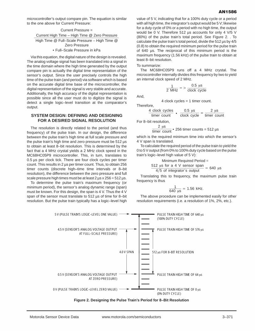
3–371Motorola Sensor Device Data www.motorola.com/semiconductors
microcontroller’s output compare pin. The equation is similarto the one above for Current Pressure:
High Time @ Full–Scale Pressure – High Time @Zero Pressure
Current High Time – High Time @ Zero Pressure
• Full–Scale Pressure in kPa
Current Pressure =
Via this equation, the digital nature of the design is revealed.The analog voltage signal has been translated into a signal inthe time domain where the high time generated by the outputcompare pin is actually the digital time representation of thesensor’s output. Since the user precisely controls the hightime of the pulse train (and period) via software which is basedon the accurate digital time base of the microcontroller, thedigital representation of the signal is very stable and accurate.Additionally, the high accuracy of the digital representation ispossible since all the user must do to digitize the signal isdetect a single logic–level transition at the comparator’soutput.
SYSTEM DESIGN: DEFINING AND DESIGNINGFOR A DESIRED SIGNAL RESOLUTION
The resolution is directly related to the period (and thusfrequency) of the pulse train. In our design, the differencebetween the pulse train’s high time at full scale pressure andthe pulse train’s high time and zero pressure must be 512 µsto obtain at least 8–bit resolution. This is determined by thefact that a 4 MHz crystal yields a 2 MHz clock speed in theMC68HC05P9 microcontroller. This, in turn, translates to0.5 µs per clock tick. There are four clock cycles per timercount. This results in 2 µs per timer count. Thus, to obtain 256timer counts (discrete high–time time intervals or 8–bitresolution), the difference between the zero pressure and fullscale pressure high times must be at least 2 µs x 256 = 512 µs.
To determine the pulse train’s maximum frequency (orminimum period), the sensor’s analog dynamic range (span)must be known. For this design, the span is 4 V. Thus the 4 Vspan of the sensor must translate to 512 µs of time for 8–bitresolution. But the pulse train typically has a logic–level high
value of 5 V, indicating that for a 100% duty cycle or a periodwith all high time, the integrator’s output would be 5 V; likewisefor a duty cycle of 0% or a period with no high time, the outputwould be 0 V. Therefore 512 µs accounts for only 4 V/5 V(80%) of the pulse train’s total period. See Figure 2. . Tocalculate the pulse train’s total period, divide the 512 µs by 4/5(0.8) to obtain the required minimum period for the pulse trainof 640 µs. The reciprocal of this minimum period is themaximum frequency (1.56 kHz) of the pulse train to obtain atleast 8–bit resolution.
To summarize:The MC68HC05P9 runs off a 4 MHz crystal. The
microcontroller internally divides this frequency by two to yieldan internal clock speed of 2 MHz.
12 MHz
0.5 s
clock cycle
And,4 clock cycles = 1 timer count.
Therefore,4 clock cycles
timer count0.5 s
clock cycle
2 stimer count•
For 8–bit resolution,2 s
timer count • 256 timer counts = 512 µs
which is the required minimum time into which the sensor’s4 V span is translated.
To calculate the required period of the pulse train to yield the0 to 5 V output (from 0% to 100% duty cycle based on the pulsetrain’s logic–level high value of 5 V):
512 s for a 4 V sensor span45 of integrators output
640 s
Minimum Required Period =
Translating this to frequency, the maximum pulse trainfrequency is thus
1640 s
1.56 kHz.
The above procedure can be implemented easily for otherresolution requirements (i.e. a resolution of 1%, 2%, etc.).
Figure 2. Designing the Pulse Train’s Period for 8–Bit Resolution
5 V (PULSE TRAIN’S LOGIC–LEVEL ONE VALUE)
4.5 V (SENSOR’S ANALOG VOLTAGE OUTPUTAT FULL–SCALE PRESSURE)
0.5 V (SENSOR’S ANALOG VOLTAGE OUTPUTAT ZERO PRESSURE)
0 V (PULSE TRAIN’S LOGIC–LEVEL ZERO VALUE)
4.0 V SPAN
PULSE TRAIN HIGH TIME OF 640 s(100% DUTY CYCLE)
PULSE TRAIN HIGH TIME OF 576 s
PULSE TRAIN HIGH TIME OF 64 s
512 s FOR 8–BIT RESOLUTION
PULSE TRAIN HIGH TIME OF 0 s(0% DUTY CYCLE)

3–372 Motorola Sensor Device Datawww.motorola.com/semiconductors
Important Note:Very small and very large high times (assuming a fixed
period) are typically unattainable due to the finite amount oftime it takes to generate the pulse train on the output comparepin. This amount of time will vary depending on themicrocontroller’s clock speed and the latency of the actualsoftware routines implemented. Thus the sensor’s analogvoltage to which the integrator’s dc voltage is compared mustbe within the possible ranges of voltages created by theintegrator’s input pulse train — i.e. the sensor’s zero pressureoffset voltage must be greater than the smallest voltagecreated by the integrator (corresponding to the pulse train’ssmallest possible high time) and the sensor’s full scale outputvoltage must be less than the largest voltage created by theintegrator (corresponding to the pulse train’s largest possiblehigh time).
After establishing the frequency of the pulse train, the RCtime constant for the integrator can be determined and theresistor and capacitor value can be chosen. The RC timeconstant should be long compared to the period of the pulsetrain so that a stable dc voltage (very little ripple due to thecapacitor’s charging and discharging) is obtained at the outputof the comparator.
Follow these steps to design the RC time constant andintegrator’s component values. The design example’scalculations are presented simultaneously.
For the resolution desired, determine the number of volts(typically mV) that corresponds to the least significant bit (onetimer count). For this design example, 8–bit resolution (256timer counts) over the desired pressure sensor spancorresponds to
# of mVtimer count
Desired Pressure Sensor Span (V)Number of Timer Counts
4 V256 timer counts
15.6 mVtimer count
Therefore the stability of the integrator’s output voltageshould be less than 15.6 mV (least significant bit). Choosingan RC time constant that allows a ripple of approximatelyone–fourth of the least significant bit is sufficient(approximately 3.9 mV).
The most ripple occurs at a 50% duty cycle pulse train. Forthis design the entire period is 640 µs. 50% duty cycleindicates a high time (and low time) of 320 µs. Furthermore,the capacitor should discharge no more than approximately3.9 mV (defined as ∆V) over the 320 µs. The followingequation is used to calculate the value for RC:
tRC
V(t) = Vinitial – ∆V = Pulse Train Logic–level one value •
Duty Cycle • e
where Vinitial = Pulse Train Logic–level one value • Duty Cycleand ∆V is the voltage discharge of the capacitor.
Solving for RC:
t
ln V(t)Pulse Train Logic–level one value Duty Cycle
•
RC = –
320 s
ln 2.5 V – 3.9 mV5 V 50%
0.205 s
•
Finally, choose the values of the resistor and capacitor. Atypical resistor value is on the order of a tens of kΩ. Theresistor’s value can be higher (hundreds of kΩ) but care mustbe taken to avoid increased thermal noise.
For this design, the resistor value is chosen to be 49.9 kΩ(1% resistor). The capacitor’s value is readily calculated to be
C 0.205 s49.9 k
4.1 F
Choose the values of the resistor and capacitor so that theactual time constant is equal to or greater than the calculatedtime constant.
Note: Be aware that temperature variations can createerrors in the system (thus reducing system performance);therefore, be sure to use low temperature coefficient resistors,capacitors, etc.
SYSTEM DESIGN: STEP–BY–STEP PROCEDUREFOR PRESSURE MEASUREMENT AND
CALIBRATION
To measure pressure (note: there are other measurementalgorithms that can be performed that in some cases may bemore acceptable (see below, Additional notes)):
1. Start with a pulse train with the minimum high timefeasible with the system’s microcontroller. Pulse trainshould run at a frequency equal to or less than thefrequency calculated above.
2. Make sure the general I/O pin’s input is high (sensor’soutput voltage is greater than the integrator’s outputvoltage).
3. Increment the high time of the pulse train by one timercount.
4. Check the general I/O pin to see if its input is low(sensor’s output voltage has become less than theintegrator’s output voltage).
5. If the general I/O pin is reading a logic–level zero, store inmemory the high time of the pulse train as the currentpressure high time reading that created the logic–leveltransition in the comparator’s output.
6. If the general I/O pin is reading a logic–level one, go backto step 3 and repeat.
7. Using the equation “Current Pressure = .......” shownabove, calculate the current pressure (assuming thesystem has already been calibrated).
8. Repeat steps 1 through 7 for additional pressuremeasurements.
To calibrate the system:At zero and full scale pressures, perform the above 8 step
pressure measurement routine. Store the appropriate pulsetrain high times corresponding to zero and full scale pressure.These high times will be used to calculate the current pressureas mentioned in Step 7 above.
SOFTWARE EXAMPLES TO GENERATE PULSETRAIN ON OUTPUT COMPARE TIMER CHANNEL
The following software examples are written in assemblylanguage for the MC68HC05P9 (the code is applicable to anyHC05 series microcontroller with TCMP pin).

3–373Motorola Sensor Device Data www.motorola.com/semiconductors
* GENERATES THE PULSE TRAIN ON TCMPGEN
LDA PERIODL * LOW BYTE OF THE PERIODSUB HIGHTIMEL * LOW BYTE OF THE HIGHTIMESTA LOWTIMEL * LOW BYTE OF THE LOWTIMELDA PERIODH * HIGH BYTE OF THE PERIODSBC HIGHTIMEH * HIGH BYTE OF THE HIGHTIMESTA LOWTIMEH * HIGH BYTE OF THE LOWTIMERTS
* INCREASE THE HIGH TIME (DUTY CYCLE) OF THE PULSE TRAININCPW
LDA HIGHTIMELADD #$01 * INCREMENT PULSE WIDTH BY 2 µsSTA HIGHTIMELLDA HIGHTIMEHADC #$0STA HIGHTIMEHRTS
* DECREASE THE HIGH TIME (DUTY CYCLE) OF THE PULSE TRAINDECPW
LDA HIGHTIMELSUB #$01 * DECREMENT PULSE WIDTH BY 2 µsSTA HIGHTIMELLDA HIGHTIMEHSBC #$0STA HIGHTIMEHJSR GENRTS
* INCREASE THE PERIOD (DECREASE FREQUENCY) OF THE PULSE TRAININCPER
LDA PERIODLADD #$05 * INCREMENT PERIOD BY 10 µsSTA PERIODLLDA PERIODHADC #$0 * ADJUST HIGH BYTE OF PERIOD IF CARRYSTA PERIODHJSR GENRTS
* DECREASE THE PERIOD (INCREASE FREQUENCY) OF THE PULSE TRAINDECPER
LDA PERIODLSUB #$05 * DECREMENT PERIOD BY 10 µsSTA PERIODLLDA PERIODHSBC #$0 * ADJUST HIGH BYTE OF PERIOD IF BORROWSTA PERIODHJSR GENRTS
TIMER * INTERRUPT SERVICE ROUTINE FOR TCMPLDA TSR * CLEAR OCF FLAG IN TSRLDA TCMPL
BRSET 0,TCR,ADDHIGH * HIGH OR LOW PULSE TIME NEEDED?
ADDLOWBSET 0,TCR * ADD LOW TIME TO THE PULSE TRAINLDA LOWTIMELADD TCMPLTAXLDA TCMPHADC LOWTIMEHSTA TCMPHSTX TCMPLRTI
ADDHIGHBCLR 0,TCR * ADD HIGH TIME TO THE PULSE TRAINLDA HIGHTIMELADD TCMPLTAXLDA TCMPHADC HIGHTIMEHSTA TCMPHSTX TCMPLRTI

3–374 Motorola Sensor Device Datawww.motorola.com/semiconductors
ADDITIONAL NOTES
This type of A/D conversion method (one type of A/Dconversion) inherently takes a finite period of time to digitizethe signal (incrementing the pulse train’s high time whilepolling the general I/O pin); however, for most sensorapplications the physical phenomenon being measured doesnot change quickly (<1 ms) enough to warrant an ultra–fastA/D conversion process.
An additional advantage of this design is that themeasurement process may be performed only as necessary,keeping the CPU processing time and overhead minimal.
If an input capture timer channel (TCAP) is available, it maybe configured to detect the logic–level one to logic–level zerotransition of the comparator’s output. When the edgetransition occurs, an interrupt service routine is executed thatstores the pulse train’s high times, calculates the current
pressure, etc. This is typically more convenient and eliminatesthe need to poll a general I/O pin every time the pulse train’shigh time is incremented (interrupt subroutine is executed onlywhen the edge transition occurs).
SUMMARY
Shown above is a minimal component design that canconvert an analog sensor’s output into a digital output. Eachmajor subsystem (sensor, amplifier, integrator, comparator,and microcontroller) is explained in detail simultaneously witha design example. Next the system operation is discussedincluding how it works and how to design a desired systemresolution. Finally a flow chart for measuring and calibratingthe sensor’s output is presented.

3–375Motorola Sensor Device Data www.motorola.com/semiconductors
Prepared by Ador ReodiqueMotorola Sensor Systems and Applications Engineering
INTRODUCTIONThis application note describes how to implement an auto–
zero function when using a Motorola integrated pressure sen-sor with a microcontroller and an analog to digital converter(MCU and an A/D). Auto–zero is a compensation techniquebased on sampling the offset of the sensor at reference pres-sure (atmospheric pressure is a zero reference for a gaugemeasurement) in order to correct the sensor output for long–term offset drift or variation.
Sources of offset errors are due to device to device offset vari-ation (trim errors), mechanical stresses (mounting stresses),shifts due to temperature and aging. Performing auto–zero willgreatly reduce these errors. The amount of error correction islimited by the resolution of the A/D.
In pressure sensing applications where a zero–pressurereference condition can exist, auto–zero can be implementedeasily when an integrated pressure sensor is interfaced toan MCU.
EFFECTS OF OFFSET ERRORSFigure 1 illustrates the transfer function of an integrated
pressure sensor. It is expressed by the linear function:
VOUT = VOFF + [(VFSO VOFF)/(PMAX PREF)]*P= VOFF + S*P.
Here, VOUT is the voltage output of the sensor, VFSO is thefull–scale output, VOFF is the offset, PMAX is the maximumpressure and PREF is the reference pressure. Note that (VFSOVOFF/PMAX PREF) can be thought of as the slope of the lineand VOFF as they y–intercept. The slope is also referred to asthe sensitivity, S, of the sensor.
Figure 1. Definition of Span, Full–Scale Output,Offset and Sensitivity
SENSOR OUTPUT
VFSO
VOFF
PREF PMAX
PRESSURE
SPAN
S
A two–point pressure calibration can be performed toaccurately determine the sensitivity and get rid of the offsetcalibration errors altogether. However, this can be veryexpensive in a high volume production due to extra time andlabor involved. The system designer therefore designs apressure sensor system by relying on the sensitivity and offsetdata given in the data sheet and using a linear equation todetermine the pressure. Using the later, the sensed pressureis easily determined by:
P = (VOUT VOFF)/S.
If an offset error is introduced due to device to device varia-tion, mechanical stresses, or offset shift due to temperature(the offset has a temperature coefficient or TCO), those errorswill show up as an error, ∆P, in the pressure reading:
P + ∆P = [VOUT (VOFF + ∆VOFF)]/S.
As evident in Figure 2, offset errors, ∆VOFF, have the effectof moving the intercept up and down without affecting thesensitivity. We can therefore correct this error by sampling thepressure at zero reference pressure (atmosphere) andsubtracting this from the sensor output.
Figure 2. Effect of Offset Errors
SENSOR OUTPUT VOUT
VFSO
VOFF
PREF(atm) PMAX
PRESSURE
∆VOFF
VP
∆P
P
AUTO–ZERO CONSIDERATIONSIN APPLICATIONS
There is an important consideration when implementingauto–zero. In order to use this technique, a zero pressurereference condition must be known to exist in the system.
SEMICONDUCTOR APPLICATION NOTE
REV 1

3–376 Motorola Sensor Device Datawww.motorola.com/semiconductors
There are a lot of applications that will lend themselvesnaturally to auto–zeroing. Typical applications are those that:
• experience a zero–pressure condition at system start up,
• are idle for a long time (zero pressure), take a pressuremeasurement then go back to idle again.
For example, in a water level measurement in a washingmachine application, there is a zero pressure referencecondition when the water in the tub is fully pumped out.Another application that is perfect for auto–zeroing is abeverage fill level measurement; a zero reference conditionexists before the bottle is filled. HVAC air flow applications canalso use auto–zeroing; before system start up, an auto–zerocan be initiated. In other words, it can be used in applicationswhere a zero pressure condition can exist in order toauto–zero the system.
An auto–zero command can be automated by the systemor can be commanded manually. Each system will have adifferent algorithm to command an auto–zero signal. Forexample, using the beverage fill level measurement as anexample, the system will auto zero the sensor before the bottleis filled.
IMPLEMENTATION OF AUTO–ZERO WITH AMICROCONTROLLER
Auto–zero can be implemented easily when the integratedsensor is interfaced to a microcontroller. The auto–zeroalgorithm is listed below:
1. Sample the sensor output when a known zero refer-ence is applied to the sensor (atmospheric pressure isa zero reference for gauge type measurement). Storecurrent zero pressure offset as CZPO.
2. Sample the sensor output at the current appliedpressure. Call this SP.
3. Subtract the stored offset correction, CZPO, from SP.The pressure being measured is simply calculated as:
PMEAS = (SPCZPO)/S.
Note that the equation is simply a straight line equation,where S is the sensitivity of the sensor. The auto–zeroalgorithm is shown graphically in Figure 3.
Figure 3. Flow–Chart of the Auto–Zero Algorithm
Start
Sample Current Zero Offset, CZPO
Sample Current Pressure, SP
PMEASCPCZPO
S
Calculate Pressure
measure again auto–zero command received
End

3–377Motorola Sensor Device Data www.motorola.com/semiconductors
IMPROVEMENT ON OFFSET ERROR
In the following calculations, we will illustrate how auto–zerowill improve the offset error contribution. We will use theMPXV4006G interfaced to an 8–bit A/D as an example. Whenauto–zero is performed, the offset errors are reduced and theresulting offset errors are replaced with the error (due toresolution) of the A/D. We can categorize the offset errorcontributions into temperature and calibration errors.
Temperature Coefficient of Offset ErrorThe offset error due to temperature is due to Temperature
Coefficient of Offset, or TCO. This parameter is the rate ofchange of the offset when the sensor is subject totemperature. It is defined as:
TCO = (∆VOFF/∆T).
The MPXV4006G has a temperature coefficient of offset(normalized with the span at 25°C) of:
∆TCO = (∆VOFF/∆T)/VFS@25°C = 0.06% FS/°C.
As an example, if the sensor is subjected to temperaturerange between 10°C and 60°C, the error due to TCO is:
∆TCO = (0.06% FS/C)*(60°C 10°C) = 3.0% FS.
Offset Calibration ErrorsEven though the offset is laser trimmed, offset can shift due
to packaging stresses, aging and external mechanicalstresses due to mounting and orientation. This results in offsetcalibration error. For example, the MPXV4006G data sheetshows this as:
VOFF MIN = 0.100 V, VOFF TYPICAL = 0.225 V and VOFF MAX = 0.430 V.
We can then calculate the offset calibration error withrespect to the full scale span as:
∆VOFF MIN,MAX = (VOFF TYPICAL VOFF MIN,MAX)/VFS.
This results in the following offset calibration error,
∆VOFF MIN = 2.7% FS and∆VOFF MAX = 4.5% FS.
A/D ErrorAs mentioned above, we can reduce offset errors
(calibration and TCO) when we perform auto–zero. Theseerrors are replaced with the A/D error (due to its resolution),
∆OFFSETAUTOZERO = ∆TCO + ∆OFFSET = ∆A/D.
Typically, a sensor is interfaced to an 8–bit A/D. With the A/Dreference tied to VRH = 5 V and VRL = 0 V, the A/D can resolve19.6 mV/bit. For example, the MXPV4006G has a sensitivityof 7.5 mV/mmH20, the resolution is therefore,
A/DRESOLUTION = 19.6 mV/bit)/(7.5 mV/mmH20)= 2.6 mmH20/bit.
Assuming +/1 LSB error, the error due to digitization andthe resulting offset error is,
∆A/D = ∆OFFSETAUTOZERO = 2.6 mmH20/612 mmH20= +/ 0.4% FS.
It can be seen that with increasing A/D resolution, offseterrors can be further reduced. For example, with a 10–bit A/D,the resulting offset error contribution is only 0.1% FS whenauto–zero is performed.
If auto–zero is to be performed only once and offsetcorrection data is stored in non–volatile memory, the TCOoffset error and calibration error will not be corrected if thesensor later experiences a wide temperature range or laterexperience an offset shift. However, if auto–zero is performedat the operating temperature, TCO error will be compensatedalthough subsequent offset calibration error will not becompensated. It is therefore best to auto–zero as often aspossible in order to dynamically compensate the system foroffset errors.
CONCLUSION
Auto–zero can be used to reduce offset errors in a sensorsystem. This technique can easily be implemented when anintegrated pressure sensor is interfaced to an A/D and amicrocontroller. With a few lines of code, the offset errors areeffectively reduced; the resulting offset error reduction islimited only by the resolution of the A/D.

3–378 Motorola Sensor Device Datawww.motorola.com/semiconductors
Prepared by Ador Reodique, Sensor and Systems Applications Engineering and Warren Schultz, Field Engineering
INTRODUCTION
Motorola Integrated Pressure Sensors (IPS) have trimmedoutputs, built–in temperature compensation and an amplifiedsingle–ended output which make them compatible withAnalog to Digital converters (A/D’s) on low cost micro–control-lers. Although 8–bit A/D’s are most common, higher resolutionA/D’s are becoming increasingly available. With these higherresolution A/D’s, the noise that is inherent to piezo–resistivebridges becomes a design consideration.
The two dominant types of noise in a piezo–resistive inte-grated pressure sensor are shot (white) noise and 1/f (flickernoise). Shot noise is the result of non–uniform flow of carriersacross a junction and is independent of temperature. Thesecond, 1/f, results from crystal defects and also due to waferprocessing. This noise is proportional to the inverse of fre-quency and is more dominant at lower frequencies3.
Noise can also come from external circuits. In a sensor sys-tem, power supply, grounding and PCB layout is important andneeds special consideration.
The following discussion presents simple techniques formitigating these noise signals, and achieving excellent resultswith high resolution A/D converters.
EFFECTS OF NOISE IN SENSOR SYSTEMThe transducer bridge produces a very small differential
voltage in the millivolt range. The on–chip differential amplifieramplifies, level shifts and translates this voltage to a single–ended output of typically 0.2 volts to 4.7 volts. Although thetransducer has a mechanical response of about 500 Hz, itsnoise output extends from 500 Hz to 1 MHz. This noise isamplified and shows up at the output as depicted in Figure 1.
There is enough noise here to affect 1 count on an 8 bit A/D,and 4 or 5 counts on a 10 bit A/D. It is therefore important toconsider filtering. Filtering options are discussed as follows.
Figure 1. MPX5006 Raw Output
SEMICONDUCTOR APPLICATION NOTE
REV 1
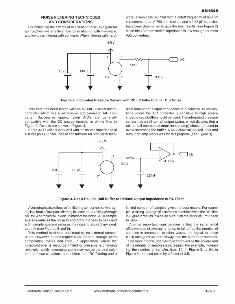
3–379Motorola Sensor Device Data www.motorola.com/semiconductors
NOISE FILTERING TECHNIQUESAND CONSIDERATIONS
For mitigating the effects of this sensor noise, two generalapproaches are effective, low pass filtering with hardware,and low pass filtering with software. When filtering with hard-
ware, a low–pass RC filter with a cutoff frequency of 650 Hzis recommended. A 750 ohm resistor and a 0.33 µF capacitorhave been determined to give the best results (see Figure 2)since the 750 ohm series impedance is low enough for mostA/D converters.
Figure 2. Integrated Pressure Sensor with RC LP Filter to Filter Out Noise
1.0 F
IPS 0.33 F
A/D3
5 V
0.01 F
750
2
1
This filter has been tested with an MC68HC705P9 micro-controller which has a successive approximation A/D con-verter. Successive approximation A/D’s are generallycompatible with the DC source impedance of the filter inFigure 2. Results are shown in Figure 4.
Some A/D’s will not work well with the source impedance ofa single pole RC filter. Please consult your A/D converter tech-
nical data sheet if input impedance is a concern. In applica-tions where the A/D converter is sensitive to high sourceimpedance, a buffer should be used. The integrated pressuresensor has a rail–to–rail output swing, which dictates that arail–to–rail operational amplifier (op amp) should be used toavoid saturating the buffer. A MC33502 rail–to–rail input andoutput op amp works well for this purpose (see Figure 3).
1.0 F
IPS 0.33 F
A/D3
5 V
0.01 F
750
2
1+
–
MC33502
Figure 3. Use a Rail–to–Rail Buffer to Reduce Output Impedance of RC Filter
Averaging is also effective for filtering sensor noise. Averag-ing is a form of low pass filtering in software. A rolling averageof 8 to 64 samples will clean up most of the noise. A 10 sampleaverage reduces the noise to about 2.5 mV peak to peak anda 64 sample average reduces the noise to about 1 mV peakto peak (see Figures 5 and 6).
This method is simple and requires no external compo-nents. However, it does require RAM for data storage, extracomputation cycles and code. In applications where themicrocontroller is resource limited or pressure is changingrelatively rapidly, averaging alone may not be the best solu-tion. In these situations, a combination of RC filtering and a
limited number of samples gives the best results. For exam-ple, a rolling average of 4 samples combined with the RC filterin Figure 2 results in a noise output on the order of 1 mV peakto peak.
Another important consideration is that the incrementaleffectiveness of averaging tends to fall off as the number ofsamples is increased. In other words, the signal–to–noise(S/N) ratio goes up more slowly than the number of samples.To be more precise, the S/N ratio improves as the square rootof the number of samples is increased. For example, increas-ing the number of samples from 10, in Figure 5, to 64, inFigure 6, reduced noise by a factor of 2.5.

3–380 Motorola Sensor Device Datawww.motorola.com/semiconductors
Figure 4. Output After Low Pass Filtering
Figure 5. Output with 10 Averaged Samples

3–381Motorola Sensor Device Data www.motorola.com/semiconductors
Figure 6. Output with 64 Averaged Samples
Figure 7. Filtered Sensor Output and Averaged Over 10 Samples

3–382 Motorola Sensor Device Datawww.motorola.com/semiconductors
POWER SUPPLYSince the sensor output is ratiometric with the supply volt-
age, any variation in supply voltage will also proportionallyappear at the output of the sensor. The integrated pressuresensor is designed, characterized and trimmed to be poweredwith a 5 V +/– 5% power supply which can supply the maxi-mum 10 mA current requirement of the sensor. Powering theintegrated sensor at another voltage than specified is not rec-ommended because the offset, temperature coefficient of off-set (TCO) and temperature coefficient of span (TCS) trim willbe invalidated and will affect the sensor accuracy.
From a noise point of view, adequate de–coupling is impor-tant. A 0.33 µF to 1.0 µF ceramic capacitor in parallel with a0.01 µF ceramic capacitor works well for this purpose. Also,with respect to noise, it is preferable to use a linear regulatorsuch as an MC78L05 rather than a relatively more noisyswitching power supply 5 volt output. An additional consider-ation is that the power to the sensor and the A/D voltage refer-ence should be tied to the same supply. Doing this takesadvantage of the sensor output ratiometricity. Since the A/Dresolution is also ratiometric to its reference voltage, varia-tions in supply voltage will be canceled by the system.
LAYOUT OPTIMIZATIONIn mixed analog and digital systems, layout is a critical part
of the total design. Often, getting a system to work properlydepends as much on layout as on the circuit design. The fol-lowing discussion covers some general layout principles, digi-tal section layout and analog section layout.
General Principles:There are several general layout principles that are impor-
tant in mixed systems. They can be described as five rules:Rule 1: Minimize Loop Areas. This is a general principle
that applies to both analog and digital circuits. Loops areantennas. At noise sensitive inputs, the area enclosed by anincoming signal path and its return is proportional to theamount of noise picked up by the input. At digital output ports,the amount of noise that is radiated is also proportional toloop area.
Rule 2: Cancel fields by running equal currents thatflow in opposite directions as close as possible to eachother. If two equal currents flow in opposite directions, theresulting electromagnetic fields will cancel as the two currentsare brought infinitely close together. In printed circuit boardlayout, this situation can be approximated by running signalsand their returns along the same path but on different layers.Field cancellation is not perfect due to the finite physical sepa-ration, but is sufficient to warrant serious attention in criticalpaths. Looked at from a different perspective, this is anotherway of looking at Rule # 1, i.e., minimize loop areas.
Rule 3: On traces that carry high speed signals avoid 90degree angles, including “T” connections. If you think ofhigh speed signals in terms of wavefronts moving down atrace, the reason for avoiding 90 degree angles is simple. Toa high speed wavefront, a 90 degree angle is a discontinuitythat produces unwanted reflections. From a practical point ofview, 90 degree turns on a single trace are easy to avoid byusing two 45 degree angles or a curve. Where two tracescome together to form a “T” connection, adding some materialto cut across the right angles accomplishes the same thing.
Rule 4: Connect signal circuit grounds to powergrounds at only one point. The reason for this constraint isthat transient voltage drops along the power grounds can besubstantial, due to high values of di/dt flowing through finite in-ductance. If signal processing circuit returns are connected topower ground at multiple points, then these transients willshow up as return voltage differences at different points in thesignal processing circuitry. Since signal processing circuitryseldom has the noise immunity to handle power ground tran-sients, it is generally necessary to tie signal ground to powerground at only one point.
Rule 5: Use ground planes selectively. Although groundplanes are highly beneficial when used with digital circuitry, inthe analog world they are better used selectively. A singleground plane on an analog board puts parasitic capacitancein places where it is not desired, such as at the inverting inputsof op amps. Ground planes also limit efforts to take advantageof field cancellation, since the return is distributed.
ANALOG LAYOUT
In analog systems, both minimizing loop areas and fieldcancellation are useful design techniques. Field cancellationis applicable to power and ground traces, where currents areequal and opposite. Running these two traces directly overeach other provides field cancellation for unwanted noise, andminimum loop area.
Figure 8 illustrates the difference between a power supplyde–coupling loop that has been routed correctly and one thathas not. In this figure, the circles represent pads, the sche-matic symbols show the components that are connected to thepads, and the routing layers are shown as dark lines (toptrace) or grey lines (bottom trace). Note that by routing the twotraces one over the other that the critical loop area is mini-mized. In addition, it is important to keep de–coupling capaci-tors close to active devices such as MPX5000–series sensorsand operational amplifiers. As a rule of thumb, when 50 milground and Vcc traces are used, it is not advisable to havemore than 1 inch between a de–coupling capacitor and theactive device that it is intended to be de–coupled.
Figure 8. Minimizing Loop Areas
SENSOR SENSOR
RECOMMENDED AVOID
+5 VGND
+5 VGND
TOP TRACE
BOT TRACE

3–383Motorola Sensor Device Data www.motorola.com/semiconductors
For similar reasons it is desirable to run sensor output sig-nals and their return traces as close to each other as pos-sible. Minimizing this loop area will minimize the amount ofexternal noise that is picked up by making electrical connec-tions to the sensor.
DIGITAL LAYOUTThe primary layout issue with digital circuits is ground
partitioning. A good place to start is with the architecture thatis shown in Figure 9. This architecture has several key attrib-utes. Analog ground and digital ground are both separateand distinct from each other, and come together at only onepoint. For analog ground it is preferable to make the one pointas close as possible to the analog to digital converter’sground reference (VREFL). The power source ground con-nection should be as close as possible to the microcontrol-ler’s power supply return (VSS). Note also that the path fromVREFL to VSS is isolated from the rest of digital ground untilit approaches VSS.
DIGITAL GROUND/GROUND PLANE
POWERGROUND
SENSOR/ANALOGGROUND
VREFL VSS
Figure 9. Ground Partitioning
In addition to grounding, the digital portion of a systembenefits from attention to avoiding 90 degree angles, sincethere are generally a lot of high speed signals on the digitalportion of the board. Routing with 45 degree angles or curvesminimizes unwanted reflections, which increases noise immu-
nity. Single traces are easy, two forty five degree angles or acurve easily accomplish a 90 degree turn. It is just as importantto avoid 90 degree angles in T connections. Figure 10 illus-trates correct versus incorrect routing for both cases.
Figure 10. 90 Degree Angles
SINGLE TRACE
AVOID GOOD PRACTICE
T–CONNECTION
AVOID GOOD PRACTICE
CONCLUSION
Piezo–resistive pressure sensors produce small amountsof noise that can easily be filtered out with several methods.These methods are low pass filtering with an RC filter, averag-ing or a combination of both which can be implemented withminimal hardware cost.
In a mixed sensor system, noise can be further reduced byfollowing recommended power supply, grounding and layouttechniques.
REFERENCES
[1] AN1626 Noise Management in Motor Drives, WarrenSchultz, Motorola, Inc.
[2] Noise Reduction Techniques In Electronic Systems 2ndEdition, Henry W. Ott, John Wiley & Sons.
[3] Noise: Comparing Integrated Pressure Sensors and OpAmps, Ira Basket, Motorola Sensor Products Divisioninternal paper.

3–384 Motorola Sensor Device Datawww.motorola.com/semiconductors
Prepared by: Warren Schultz
PSPICE models for Uncompensated, MPX2000 series, andMPX5000 series pressure sensors are presented here. Thesemodels use compound coefficients to improve modeling oftemperature dependent behavior. The discussion begins withan overview of how the models are structured, and is followedby an explanation of compound coefficients. The emphasis ison how to use these models to estimate sensor performance.They can be found electronically on a disk included in ASB200Motorola Sensor Development Controller kits, and on theWEB at:
http://www.mot–sps.com/home2/models/bin/sensor2.html
MODEL STRUCTURE
Models for all three sensors series share a commonstructure. They are complete models set up to run as is. Toobtain output voltage versus pressure, it is only necessary torun the model and display V(2,4) or V(1,0). V(2,4) gives theoutput voltage for Uncompensated and MPX2000 seriessensors. V(1,0) applies to MPX5000 sensors. In both cases,V(2,4) and V(1,0) correspond to the pin numbers where outputvoltage would be, if probed on an actual part.
These models are divided into five sections to facilitate easeof use. They are:
• INPUT PARAMETERS
• LINEAR TO COMPOUND CONVERSION
• MODEL COEFFICIENTS
• TRANSDUCER
• STIMULUS
Each of these sections is described in the following discussion.
INPUT PARAMETERSThis section contains input parameters that describe
measurable sensor characteristics. Inputs such as full scalepressure (FSP), full scale span (FSS) offset voltage(VOFFSET), and temperature coefficient of offset voltage(TCOS) are made here. Characteristics that are specific to thetransducer, such as bridge impedance (RBRIDGE),temperature coefficient of bridge resistance (TCRB), andtemperature coefficient of span (TCSP) are also listed here.
Parameters such as VOFFSET that set an output value forthe sensor are used to calculate resistance values thatproduce those outputs. For example, if you input 100 mV ofoffset voltage and a 10 µV/degree temperature coefficient ofoffset voltage, the model will calculate the bridge resistancevalues necessary to produce 100 mV of offset voltage and a10 µV/degree temperature coefficient.
In the MPX2000 and MPX5000 models, temperaturecoefficient of span (TCSP) is handled differently than the otherparameters. The non–linear behavior of span overtemperature is calculated from the interaction of thetransducer’s temperature coefficient of span (TCSP), thetransducer’s temperature coefficient of resistance (TCRB),and the effects of inserting fixed resistance, RTCSPAN, inseries with the bridge. The result is a temperature coefficientof span that closely resembles the real thing, but is not directlycontrolled by the user.
LINEAR TO COMPOUND CONVERSIONThe compound coefficients used in these models are from
equations of the form:
(1) R(Temp) = R25(1 TCR)(Temp – 25)
where R25 is resistance at 25 degrees Celsius , TCR istemperature coefficient of resistance, Temp is an abbreviationfor Temperature in degrees Celsius, and R(Temp) is thefunction resistance versus temperature.
The TCR (temperature coefficient of resistance) in equation(1) is a different number than a temperature coefficient that isstated in linear terms. The three statements in this sectionconvert linear coefficients to the compound values that themodels need. This conversion is based upon a 100 degreedifference between the two points at which the linearcoefficients have been measured.
MODEL COEFFICIENTSIn this section most of the calculation is performed. Values
for the transducer bridge resistors are determined frompressure, temperature, offset, temperature coefficient ofoffset, span, temperature coefficient of span, and temperaturecoefficient of resistance inputs. A series of parameterstatements are used, as much as is practical, to docalculations that will fit in an 80 character line withoutwraparounds. These calculations use PSPICE’s.PARAMETER function, making the models specific toPSPICE. Parameters are described as follows:
KP — Pressure constant; translates pressure into a bridgeresistance multiplier
KO — Offset constant; offset component of bridgeresistance
DT — Delta temperature; Temperature 25 degreesCelsius
KTCO — Temperature coefficient of offset constant; trans-lates temperature coefficient of offset into bridge resistance
SEMICONDUCTOR APPLICATION NOTE
REV 1

3–385Motorola Sensor Device Data www.motorola.com/semiconductors
TCR — Temperature coefficient of bridge resistance;shaped by a Table that accounts for cold temperaturenon–linearity’s
TCR2 — Temperature coefficient of contact resistance;shaped by a Table that accounts for cold temperaturenon–linearity’s
TCS — Temperature coefficient of Span; shaped by a Tablethat accounts for cold temperature non–linearity’s
RPH — Bridge Resistance (RS1 and RS3) modified bypressure and temperature
ROH — Offset Component of Bridge Resistors RS1 and RS3
RPL — Bridge Resistance (RS2 and RS4) modified bypressure and temperature
ROL — Offset Component of Bridge Resistors RS2 and RS4
KB — Bias Constant; adjusts KP for bias voltage effects ofspan compensation network (MPX2000 and MPX5000series sensors)
KBT — Bias Constant; adjusts KO for bias voltage effects ofspan compensation network (MPX2000 and MPX5000series sensors)
GAIN — Instrumentation amplifier gain; differential gain(MPX5000 series)
ROFF — Offset resistance; determines value of RS13(MPX5000 series)
After these calculations are made, the final bridge resis-tance calculation is performed in the circuit section. The valuefor bridge resistors RS1 and RS3 is RPH + ROH. Bridge resis-tors RS2 and RS4 are equal to RPL–ROL.
CIRCUITThree circuits are used to model the three sensor families,
one each for the Uncompensated series, MPX2000 series,and MPX5000 series sensors. Schematics that are derivedfrom the circuit netlists are shown in Figures 1, 2, and 3. Theyare discussed beginning with the Uncompensated series,which is the least complex.
Uncompensated Series:The Uncompensated Series sensors (MPX10, MPX50, and
MPX100) are modeled as Wheatstone bridges. In the configu-ration that is shown in Figure 1, resistors RS2 and RS4decrease in value as pressure is applied. Similarly, RS1 andRS3 increase in value as pressure is applied. Resistors RS5and RS7 are contact resistors. They represent real physicalresistors that are used to make contact to the bridge. ResistorsRS6 and RS8 are included to satisfy PSPICE’s requirementfor no floating nodes. That’s it. The netlist in this model is quitesimple. The hard part is calculating the values for RS1, RS2,RS3, and RS4.
Figure 1. MPX10 and 100 PSPICE Compound Coefficient Model
3
0
24 5 1
**
**
**
**
* *
NOTES:
* TEMPERATURE SENSITIVE* * TEMPERATURE & PRESSURE SENSITIVE
RS4475
RS1 475
RS2475
RS3475
RS81000MEG
RS7
675
RS5
750
RS61000MEG

3–386 Motorola Sensor Device Datawww.motorola.com/semiconductors
MPX2000 Series:The MPX2000 Series sensors (MPX2010, MPX2050,
MPX2100, and MPX2200) add span compensation and trimresistors to the Uncompensated model. These resistors areshown in Figure 2 as RS9, RS11, and RS10. The temperaturecoefficient of resistance (TCR) for the bridge resistors worksagainst fixed resistors RS9 and RS11 to produce a bias to thebridge that increases with temperature. This increasing biascompensates for the temperature coefficient of span, which isnegative.
Resistor RS12 is also added to the Uncompensated model.It represents additional impedance that is associated with theMPX2000 series sensors’ offset trim network. Offset perfor-mance is modeled behaviorally. Inputs for offset (VOFFSET)and temperature coefficient of offset (TCOS) are translatedinto bridge resistance values that produce the specified per-formance. This behavioral approach was chosen in order tomake it easy to plug in different values for VOFFSET andTCOS.
Figure 2. MPX2000 Series PSPICE Compound Coefficient Model
6
0
24 5 1
3
7
8
**
**
**
**
* *
NOTES:
* TEMPERATURE SENSITIVE* * TEMPERATURE & PRESSURE SENSITIVE
RS11
RS4
RS1 RS2
RS3
RS9
RS8
RS7 RS12
RS5
RS6
RS10
MPX5000 Series:The MPX5000 Series sensors (MPX5010, MPX5050,
MPX5100, MPX5700, and MPX5999) add an instrumentationamplifier to the MPX2000 series model. This amplifier isshown in Figure 3. It consists of operational amplifiers ES1,ES2, ES3, and ES4. Amplifiers ES1, ES2 and ES3 are mod-
eled as voltage controlled voltage sources with gains of100,000. Offset voltage, input bias current effects, etc. are tak-en into account with the values that are used to determine off-set voltage and temperature coefficient of the sensor bridge.Amplifier ES4 models saturation voltage. Its output follows theoutput of ES3 with saturation limits at 75 millivolts and 4.9 volts.

3–387Motorola Sensor Device Data www.motorola.com/semiconductors
Figure 3. MPX5000 Series PSPICE Compound Coefficient Model
6
5 14
3
7
**
**
**
**
* *
NOTES:
* TEMPERATURE SENSITIVE* * TEMPERATURE & PRESSURE SENSITIVE
0
8 11 13
1210
9
24
1
RS2350
RS3350
RS7
675
RS10
RS91350
RS61000MEG
RS1 350
RS4350
RS5
750
RS11
1K
RS81000MEG
RS17
112K
RS16
500
V(1,0)
RS13265.5
RS1210K
ES3
G=100,000
+–
ES1
G=100,000
+–
ES2
G=100,000
+–
RS14
112K
RS15
500
ES4
+–
STIMULUSThe last section of these models is labeled STIMULUS. Bias
voltage, pressure, and temperature are applied here. Nominalbias voltage (VCC) is 3.0 volts for Uncompensated sensors,10.0 volts for MPX2000 sensors, and 5.0 volts for MPX5000sensors. Pressure is selected on the second line. It is effectivewhen the * on line 4 is removed to command a temperaturesweep. Line 3 calls for a sweep of pressure and temperature.An * placed in front of Line 3 allows the temperature sweep online 4 to be selected.
COMPOUND COEFFICIENTS
Applying temperature coefficients to variables such asresistance is an essential part of modeling. The linearapproach, that is usually used, is based upon the assumptionthat changes are small, and can be modeled with a linearapproximation. Using temperature coefficient of resistance as(TCR) as an example, the linear expression takes the form:
(2) R(Temp) = R25(1 TCR(Temp – 25))
Provided that the TCR in equation (2) is 100 parts per millionper degree Celsius or less this approach works quite well. Withsensor TCR’s of several thousand parts per million per degreeCelsius, however, the small change assumption does nothold. To accurately model changes of this magnitude, themathematical expression has to describe a physical processwhere a unit change in temperature produces a constant per-
centage change in resistance. For example, a 1% per degreeTCR applied to a 1 K Ohm resistor should add 10 ohms to theresistor’s value going from 25 to 26 degrees. At 70 degrees,where the resistor has increased to 2006 Ohms, going from 70to 71 degrees should add 20.06 Ohms to its value. The errorin the linear expression comes from that fact that it adds 10ohms to the resistor’s value at all temperatures.
A physical process whereby a unit change in temperatureproduces a constant percentage change in resistance is easi-ly modeled by borrowing an expression from finance. Com-pound interest is a direct analog of temperature coefficients.With compound interest, a unit change in time produces aconstant percentage change in the value of a financial instru-ment. It can be described by the expression:
(3) Future Value = Present Value (1 i)n
where i is the interest rate and n is the number of periods.Substituting R25 for Present Value, R(Temp) for Future Value,TCR for i, and (Temp – 25) for n yields:
(4) R(Temp) = R25(1 TCR)(Temp 25)
Equation (4) works quite well, provided that TCR is constantover temperature. When modeling semiconductor resistors, itis also necessary to account for variable TCR’s. At cold, theTCR for p type resistors changes with temperature. Thesechanges are modeled using TABLE functions that have 3 val-ues for TCR. Results of this modeling technique versus actualmeasurements and a linear model are summarized in Table 1.

3–388 Motorola Sensor Device Datawww.motorola.com/semiconductors
Table 1. Actual versus Modeled R(Temp)
Temp Measured
R(Temp)
Compound
Model
Linear
Model
40 406 406 372
25 418 418 395
0 445 445 434
25 474 474 474
50 509 508 513
75 545 545 552
100 585 584 592
125 627 626 632
150 671 671 671
In Table 1, 25 and 150 degree Celsius data points were usedto determine both linear and compound temperature coeffi-cients. Therefore, measured values, linear model values andcompound model values all match at these two temperatures.At other temperatures, the linear model exhibits errors that aresignificant when modeling piezoresistive pressure sensors.The compound model, however, tracks with measured valuesto within 1 Ohm out of 500 Ohms.
EXAMPLES
Two examples of what the model outputs look like areshown in Figures 4 and 5. Figure 4 shows a sweep of pressureversus output voltage (VOUT) at 0, 25, and 85 degrees Celsius,for an MPX2010 sensor. It has the expected 0 to 25 mV outputvoltage, given a 0 to 10 kPa pressure input. At these threetemperatures, compensation is sufficiently good that all threeplots look like the same straight line.
Figure 4. MPX2010 V OUT versus Pressure and Temperature
To produce the plot in Figure 4, the stimulus section is setup as follows, and V(2,4) is probed.
***************************STIMULUS****************************VCC 6 0 DC=10; DC BIAS FROM PIN 3 TO PIN 1.PARAM PRESSURE=0; INPUT PRESSURE (kPa).DC PARAM PRESSURE 0_Kpa 10_Kpa .5_Kpa TEMPLIST 0 25 85*.DC PARAM TEMP –40 125 5*
This is the default configuration with which the model isshipped. To change to a sweep of zero pressure voltage ver-sus temperature, an asterisk is placed on line 3 and removedfrom line 4. The stimulus section then looks as follows:
****************************STIMULUS***************************VCC 6 0 DC=10; DC BIAS FROM PIN 3 TO PIN 1.PARAM PRESSURE=0; INPUT PRESSURE (kPa)*.DC PARAM PRESSURE 0_Kpa 10_Kpa .5_Kpa TEMPLIST 0 25 85.DC PARAM TEMP –40 125 5*
Again, V(2,4) is probed. The resulting output appears inFigure 5.
This plot shows offset versus temperature performance thatis typical of MPX2000 series sensors. From 40 to 85degrees Celsius, offset compensation is quite good. Above 85degrees there is a hook in this curve, that is an important attrib-ute of the sensor’s performance.
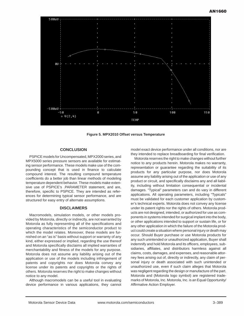
3–389Motorola Sensor Device Data www.motorola.com/semiconductors
Figure 5. MPX2010 Offset versus Temperature
CONCLUSION
PSPICE models for Uncompensated, MPX2000 series, andMPX5000 series pressure sensors are available for estimat-ing sensor performance. These models make use of the com-pounding concept that is used in finance to calculatecompound interest. The resulting compound temperaturecoefficients do a better job than linear methods of modelingtemperature dependent behavior. These models make exten-sive use of PSPICE’s .PARAMETER statement, and are,therefore, specific to PSPICE. They are intended as refer-ences for determining typical sensor performance, and arestructured for easy entry of alternate assumptions.
DISCLAIMERS
Macromodels, simulation models, or other models pro-vided by Motorola, directly or indirectly, are not warranted byMotorola as fully representing all of the specifications andoperating characteristics of the semiconductor product towhich the model relates. Moreover, these models are fur-nished on an “as is” basis without support or warranty of anykind, either expressed or implied, regarding the use thereofand Motorola specifically disclaims all implied warranties ofmerchantability and fitness of the models for any purpose.Motorola does not assume any liability arising out of theapplication or use of the models including infringement ofpatents and copyrights nor does Motorola convey anylicense under its patents and copyrights or the rights ofothers. Motorola reserves the right to make changes withoutnotice to any model.
Although macromodels can be a useful tool in evaluatingdevice performance in various applications, they cannot
model exact device performance under all conditions, nor arethey intended to replace breadboarding for final verification.
Motorola reserves the right to make changes without furthernotice to any products herein. Motorola makes no warranty,representation or guarantee regarding the suitability of itsproducts for any particular purpose, nor does Motorolaassume any liability arising out of the application or use of anyproduct or circuit, and specifically disclaims any and all liabil-ity, including without limitation consequential or incidentaldamages. “Typical” parameters can and do vary in differentapplications. All operating parameters, including “Typicals”must be validated for each customer application by custom-er’s technical experts. Motorola does not convey any licenseunder its patent rights nor the rights of others. Motorola prod-ucts are not designed, intended, or authorized for use as com-ponents in systems intended for surgical implant into the body,or other applications intended to support or sustain life, or forany other application in which the failure of the Motorola prod-uct could create a situation where personal injury or death mayoccur. Should Buyer purchase or use Motorola products forany such unintended or unauthorized application, Buyer shallindemnify and hold Motorola and its officers, employees, sub-sidiaries, affiliates, and distributors harmless against allclaims, costs, damages, and expenses, and reasonable attor-ney fees arising out of, directly or indirectly, any claim of per-sonal injury or death associated with such unintended orunauthorized use, even if such claim alleges that Motorolawas negligent regarding the design or manufacture of the part.Motorola and (Motorola logo symbol) are registered trade-marks of Motorola, Inc. Motorola, Inc. is an Equal Opportunity/Affirmative Action Employer.

3–390 Motorola Sensor Device Datawww.motorola.com/semiconductors
Prepared by Ador ReodiqueSensor and Systems Applications Engineer
INTRODUCTION
North American washing machines currently in productionuse mechanical sensors for water level measurement func-tion. These sensors are either purely mechanical pressureswitch with discrete trip points or electromechanical pressuresensor with an on–board electronics for a frequency output.
High efficiency machines require high performance sen-sors (accuracy, linearity, repeatability) even at lower pres-sure ranges. Benchmarks indicate that these performancegoals is difficult to achieve using current mechanical pres-sure sensors1.
In Europe, where energy conservation is mandated, washingmachine manufacturers have started to look at electronic solu-tions where accuracy, reliability, repeatability and additionalfunctionality is to be implemented. North American and AsiaPacific manufacturers are also looking for better solutions.
From surveys of customer requirements, a typical vertical–axis machine calls for a sensor with 600 mmH2O (24 “ H2O ~6 kPa) sensor with a 5 % FS accuracy spec. Certain appli-ances call for a lower pressure range especially in Europewhere horizontal axis machines are common.
SENSOR SOLUTIONS
For the typical 600 mmH2O, 5 % FS spec, an off the shelfsolution available today is the MPX10/MPX12, MXP2010 andthe MPXV4006G sensor. The MPX10 (or the MPX12) is 10kPa (40 “ H2O) full–scale pressure range device. It is uncom-pensated for temperature and untrimmed offset and full–scalespan. This means that the end user must temperature com-pensate as well as calibrate the full–scale offset and span ofthe device. The output of the device must be amplified usinga differential amplifier (see Figure 1) so it can be interfaced toan A/D and to obtain the desired range.
Since the MPX10/MPX12 sensors must be calibrated, theimplications of this device being used in high–volume pro-duction is expensive. Because the offset and full–scale out-put can vary from part to part, a two–point calibration isrequired as a minimum. A two point calibration is a time con-suming procedure as well as possible modification to the pro-duction line to accommodate the calibration process. The
circuitry must also accommodate for trimming, i.e., via trim-pots and/or EEPROM to store the calibration data. This addsextra cost to the system.
The MPX2010 is a 10kPa (40” H2O), temperature compen-sated, offset and full–scale output calibrated device. A differ-ential amplifier like the one shown in Figure 1 should be usedto amplify its output. Unlike the MPX10 or MPX12, this devicedoes not need a two–point calibration but auto–zeroing canimprove its performance. This procedure is easily imple-mented using the system MCU.
The MPXV4006G is a fully integrated pressure sensor spe-cifically designed for appliance water level sensing applica-tion. This device has an on board amplification, temperaturecompensation and trimmed span. An auto–zero procedureshould be implemented with this device (see Application NoteAN1636). Because expensive and time consuming calibra-tion, temperature compensation and amplification is alreadyimplemented, this device is more suitable for high volume pro-duction. The MPXV4006G integrated sensor is guaranteed tobe have an accuracy of +/–3 % FS over its pressure and tem-perature range.
For washing machine applications where low cost and highvolume productions are involved, both the MPX2010 andMPXV4006G are recommended. Both solutions can be usedin current vertical axis machines where the water level in the600 mmH2O or 24 “ H2O range. In the following, a comparisonis made between MPX2010 and MPXV4006G in terms ofsystem and performance considerations to help the customermake a decision.
EXPECTED ACCURACY OF THE MPX2010SYSTEM SOLUTION
The MPX2010 compensated sensor has an off the shelfoverall RMS accuracy of +/–7.2 % FS over 0 to 85°C tempera-ture range.
Auto–zeroing can improve the sensor accuracy to +/– 4.42% FS. However, since this sensor does not have an integratedamplification, its amplifier section must be designed carefullyin order to meet the target accuracy requirement. TheMPX2010 compensated sensor has the following specifica-tions shown on Table 1.
SEMICONDUCTOR APPLICATION NOTE

3–391Motorola Sensor Device Data www.motorola.com/semiconductors
Table 1. MPX2010 Specifications
Characteristic Min Typ Max Unit
Pressure Range 0 10 kPa
Supply Voltage 10 16 Vdc
Supply Current 6 mA
Full Scale Span 24 25 26 mV
Offset 1 1 mV
Sensitivity 25 mV/kPa
Linearity 1 1 %VFSS
Pressure Hysterisis 0.1 %VFSS
Temperature Hysterisis (40 to 125°C) 0.5 %VFSS
Temperature Effect on Span 1 1 %VFSS
Temperature Effect Offset (0 to 85°C) 1 1 mV
Input Impedance 1300 2550 ohms
Output Impedance 1400 3000 ohms
Response Time (10% to 90%) 1 ms
Warm–Up 20 ms
The sensor system errors is made up of the sensor errors,amplifier errors and A/D errors. In other words,
(1)System Sensor2 Amplifier2 ADResolution2
Table 2 shows the MPX2010 with the errors converted to%VFSS. The expected maximum root mean squared error ofthe sensor is
(2)
Sensor SpanCal2 Lin2 Phys2 Thys2 Tcs2OffCal2 Tco2OffStab2
= +/– 7.19 % FS.
With auto–zeroing, the offset calibration, temperature effecton offset and offset stability is reduced or eliminated,
Sensor SpanCal2 Lin2 Phys2 Thys2 Tcs2 (3)
= +/– 4.42 % FS.
The sensor error is calculated using the full–scale pres-sure range of the device, 0 to 85°C temperature and 10 Vexcitation.
In comparison with the MPXV4006G solution, the expectedaccuracy of the system (MPXV4006G + 8 bit A/D) withauto–zero is 3.1 % FS.
Table 2. MPX2010 span, offset and calculated maximum RMS error. *This assumes that the power supply is constant.
Span Errors (converted to %V FSS) Symbol Error Value Note Unit
Span Calibration SpanCal 4 %VFSS
Linearity Lin 1 %VFSS
Pressure Hysterisis Phys 0.1 %VFSS
Temperature Hysterisis Thys 0.5 %VFSS
Temperature Effect on Span Tcs 1.5 %VFSS
Offset Errors (converted to %V FSS)
Offset Calibration OffCal 4 %VFSS
Temperature Effect on Offset Tco 4 %VFSS
Offset Stability OffStab 0.5 %VFSS
Calculated Maximum RMS Errors RMS Error
No Compensation* 7.19 %FS
With auto–zero 4.42 %FS

3–392 Motorola Sensor Device Datawww.motorola.com/semiconductors
AMPLIFIER SELECTION ANDAMPLIFIER INDUCED ERRORS
A differential amplifier is needed to convert the differentialoutput of the MPX2010 sensor to a high level ground–
referenced (single–ended). The classic three–op amp instru-mentation amplifier can be used. However, it requires additionalcomponents (3 op–amps and possibly a split power supply). Aninstrumentation topology shown in Figure 1 requires only asingle supply and only 2 op–amps and 1% resistors.
Figure 1. MPX2010 Amplifier Circuit
VREF
+VCC
R+S2
R+S1
+–
R1
R2
2
31
R3 +–
R4
67
5
U1BVOUT_FS
+VCC
43
X1
1 2 S+
PRESSURE SENSOR
S
U1A
The circuit uses a voltage divider R+S1 and R+S2 to providethe reference (level shift), U1A and U1B are non–invertingamplifiers arranged in a differential configuration with gainresistors R1, R2, R3 and R4. Note that U1B is the main gainstage and it has the most gain. It is recommended to place a0.015 µF capacitor in it’s feedback loop (in parallel with R4) toreduce noise. The amplifier output can be characterized withthe equation below:
(4)Gain R4R3
1
(5)Voffset VREFR2·R1R1·R3
VSCMR2·R4R1·R3
1(6)Vout (S S) Gain Voffset
(7)where (S S) Sensor differential output Sensor offset
Equation 4 is the differential gain of the amplifier andequation 5 is the resulting offset voltage of the amplifier.
The above equations assume that the amplifier is close toideal (high AOL , low input offset voltage and low input offsetbias currents). Since an ideal op–amp is hard to come by, thecustomer should select an op–amp based on cost and perfor-
mance. Below are some points to keep in mind when selectingan op–amp and designing the amplifier circuit.
Note that the ratio R2*R4/R1*R3 controls the system offsetas well as the common mode error of the amplifier. Mis-matches in these resistors will result in an offset and commonmode error which appear as offset. It is therefore recom-mended to use 1% metal film resistors to reduce these errors.Also, Vref source impedance should be minimized in compari-son with R1 in order to reduce common mode error.
Amplifier input offset and input bias currents can induceerrors. For example, an input offset (Vio) of the amplifier canbecome significant when the closed–loop gain of the amplifieris increased. Furthermore, there is also a temperature coeffi-cient of the input voltage offset which contribute an additionalerror across temperature. If the input bias current of the ampli-fier is not taken into account in the design, it can also becomea source of error. A technique to reduce this error is to matchthe impedance the source impedance of what the op–ampinput pins sees.
It is important to note that high performance op–amps aremore expensive. An MC33272 op–amp has a low input offsetand low input bias current which is suitable for the two–op ampamplifier design. We can see that there is a tradeoff betweenaccuracy and cost when designing a solution with theMPX2010.

3–393Motorola Sensor Device Data www.motorola.com/semiconductors
When designing a system based on the MPX2010, it isimportant to take into account errors due to parametric varia-tion of the sensor (i.e. offset calibration, span calibration, TcS,TcO), power supply and the inherent errors of the amplificationcircuit. The offset and span errors greatly determines the reso-lution of the system (which adds to the system error). Eventhough the system offset error can be nulled out by auto–zero-ing, these errors must be accounted for when setting the sys-tem gain (see AN1556 for more details). This forces the totalspan of the system to be smaller, because we must reserve anextra headroom from the total span to account for amplifierand A/D variations (i.e. amp. sat. voltage, power supply varia-
tion, A/D quantization error, and gain errors ). If these errorsare not accounted for, it could, for example, result in non–linearity errors if the sensor span or offset error causes theamplified output of the sensor to reach the saturation voltageof the amplifier.
As an example, a MPX2010 sensor system is designedwhich has a range of 600 mmH2O FS range with a +/– 5 % FSRMS error. The system uses a +5 V +/– 5% linear regulatedpower supply, a MC33272 dual op–amp and a 1% resistors.
Table 3 shows the resulting specification and componentvalues for the system based on MPX2010 sensor.
Table 3. MPX2010 Sensor System Values
MPX2010 Sensor Design
Parameter Description Value Units
Vcc Reg Power Supply 5 V
Differential Gain Gain 433 V/V
Vout_FS Full Scale Span 3.02 V
Vref Offset Reference 0.66 V
Parts List
U1A,U1B MC33272 Op–amp
R1 Gain Resistor 39.2K Ohms
R2 Gain Resistor 90.9 Ohms
R3 Gain Resistor 909 Ohms
R4 Gain Resistor 392K Ohms
R + S1 Level Shift Resistor 1K Ohms
R + S2 Level Shift Resistor 150 Ohms
X1 MPX2010
Table 4. Performance Comparison between MPX2010 and MPXV4006G Solution
MPX2010 Solution Error(FS = 600 mmH2O)
MPXV4006G Solution Error(FS = 612 mmH2O)
Error Contribution +/– % FS +/– mmH2O +/– % FS +/– mmH2O
Max Sensor Error 7.19 43 3.00 18
System Resolution (A/D + Amplification) 1.30 8 0.80 5
System Error (Sensor + A/D + Amplification) 7.3 44 3.10 19
System Error with Auto–Zero 4.6 28 3 19
Note that the error due to system resolution is higher for theMPX2010 solution (+/– 2 bit A/D accuracy). This is becausethe MPX2010 span is limited as discussed above. Also, thisaccuracy assumes that the amplifier does not induce signifi-
cant errors. As noted MPXV4006G sensor has better overallaccuracy. The system resolution is very good because of itslarge span (4.6 V versus 3.0 V typical).

3–394 Motorola Sensor Device Datawww.motorola.com/semiconductors
SUMMARY
Several washing machine solutions were examined. TheMPX10/12 solution can be expensive in terms of additionalsupport circuitry and the added time and labor involved duringthe calibration procedure. The MPX2010 is good alternativefor high volume manufacturing because is already calibrated.With this solution, however, the system amplifier design mustbe chosen and designed carefully in order to minimize the sys-tem error. This is a consideration when deciding to implementa high accuracy solution with the MPX2010 because the costof the system will go up.
The MPXV4006G solution is geared towards high volumemanufacturing because trimming, compensation and amplifi-cation is already on board. Besides the system simplicity andusing less component, the resolution and overall accuracy ofthis solution is better than the MPX2010 solution. In some
cases, less components can actually improve the reliabilityand manufacturability the system.
REFERENCES
[1] Benchmark of Washing Machine Mechanical Sensor,Jack Rondoni, Motorola Internal Document.
[2] Mechanical Sensor Characterization, Ador Reodique,Motorola Internal Document.
[3] AN1551 Low Pressure Sensing with the MPX2010Pressure Sensor, Jeff Baum, Motorola Application Note.
[4] AN1636 Implementing Auto–Zero for Integrated PressureSensors, Ador Reodique, Motorola Application Note.
[5] AN1556 Designing Sensor Performance Specificationsfor MCU–based Systems, Eric Jacobsen and Jeff Baum,Motorola Application Note.

3–395Motorola Sensor Device Data www.motorola.com/semiconductors
By Michelle Clifford Applications Engineer Sensor Products Division Tempe, AZ
INTRODUCTION
Many washing machines that are currently in productionuse a mechanical sensor for water level detection.Mechanical sensors work with discrete trip points that enablewater level detection only at those points. The purpose for thisreference design is to allow the user to evaluate a pressuresensor for not only water level sensing to replace amechanical switch, but also for water flow measurement, leakdetection, and other solutions for smart appliances. Thissystem continuously monitors water level and water flowusing the temperature compensated MPXM2010GS pressuresensor in the low cost MPAK package, a dual op–amp, and theMC68HC908QT4, 8–pin microcontroller.
SYSTEM DESIGN
PRESSURE SENSORThe Motorola Pressure sensor family has three levels of
integration – Uncompensated, Compensated and Integrated.For this design, the MPXM2010GS compensated pressuresensor was selected because it has both temperaturecompensation and calibration circuitry on the silicon, allowinga simpler yet more robust system circuit design. An integratedpressure sensor, such as the MPXV5004G, is also a goodchoice for the design eliminating the need for the amplificationcircuitry.
The height of most washing machine tubs is 40cm,therefore the water height range that this system will bemeasuring is between 0–40cm. This corresponds to apressure range of 0 – 4 kPa. Therefore, the MPXM2010GSwas selected for this system. The sensor sensitivity is2.5mV/kPa, with a full–scale span of 25mV at the supplyvoltage of 10 Vdc. The full–scale output of the sensor changeslinearly with supply voltage, so a supply voltage of 5V willreturn a full–scale span of 12.5 mV.
(Vs actual / Vs spec) x Vout full–scale spec = Vout full–scale
(5 V/ 10 V) x 25 mV = 12.5 mV
Since this application will only be utilizing 40% of thepressure range, 0–4kPa, our maximum output voltage will be40% of the full–scale span.
Vout FS x (Percent FS Range) = Vout max
12.5 mV x 40% = 5.0 mV
The package of the pressure sensor is a ported MPAKpackage. This allows a tube to be connected to the sensor;the tube is connected to the bottom of the tub. This isolatesthe sensor from direct contact with the water. The small size,and low cost are additional features that make this package aperfect fit for this application.
Figure 1. MPXM2010GS/GST1Case 1320A
SEMICONDUCTOR APPLICATION NOTE
REV 0

3–396 Motorola Sensor Device Datawww.motorola.com/semiconductors
Table 1: MPXM2010D OPERATING CHARACTERISTICS (VS = 10 Vdc, TA = 25°C unless otherwise noted, P1 > P2)
Characteristic Symbol Min Typ Max Unit
Pressure Range(1) POP 0 — 10 kPa
Supply Voltage(2) VS — 10 16 Vdc
Supply Current Io — 6.0 — mAdc
Full Scale Span(3) VFSS 24 25 26 mV
Offset(4) Voff –1.0 — 1.0 mV
Sensitivity ∆V/∆P — 2.5 — mV/kPa
Linearity(5) — –1.0 — 1.0 %VFSS
Amplifier Selection and Amplifier Induced ErrorsThe sensor output needs to be amplified before being
inputted directly to the microcontroller through an 8–bit A/Dinput pin. To determine the amplification requirements, thepressure sensor output characteristics and the 0–5V inputrange for the A/D converter had to be considered.
The amplification circuit uses three op–amps to add anoffset and convert the differential output of the MPXM2010GSsensor to a ground–referenced, single–ended voltage in therange of 0 – 5V.
The pressure sensor has a possible offset of +/– 1mV at theminimum rated pressure. To avoid a nonlinear response whena pressure sensor chosen for the system has a negative offset(Voff), we have added a 5mV offset to the positive sensoroutput signal. This offset will remain the same regardless ofthe sensor output. Any additional offset that the sensor orop–amp introduce is compensated for by software routinesthat are invoked when the initial system calibration is done.
To determine the gain required for the system, the maximumoutput voltage from the sensor for this application had to bedetermined. The maximum output voltage from the sensor isapproximately 12.5mV with a 5V supply since the full–scaleoutput of the sensor changes linearly with supply voltage. Thissystem will have a maximum pressure of 4kPa at 40cm ofwater. At a 5V supply, we will have a maximum sensor outputof 5mV at 4kPa of pressure. To amplify the maximum sensoroutput to 5.0V, the following gain is needed:
Gain = (Max Output needed) / (Max Sensor Output andInitial Offset)
= 5.0V / (.005V + .005) = 500
The gain for the system was set for 500 to avoid railing frompossible offsets from the pressure sensor or the op–amp.
The Voltage Outputs from the sensor are each connectedto a non–inverting input of an op–amp. Each op–amp circuithas the same resistor ratio. The amplified voltage signal fromthe negative sensor lead is VA. The resulting voltage iscalculated as follows:
VA= (1+R8/R6) * V4= (1+10/1000) * V4= (1.001) * V4
The amplified voltage signal from the positive sensor leadis VB. This amplification adds a small gain to ensure that thepositive lead, V2, is always greater than the voltage outputfrom the negative sensor lead, V4. This ensures the linearityof the differential voltage signal.
VB = (1+R7/R5) * V2 – (R7/R5) * Vcc= (1+10/1000) * V2 + (10/1000)*(5V) = (1.001) * V2 + .005V
The difference between the positive sensor voltage, VB, andthe negative sensor voltage, VA is calculated and amplifiedwith a resulting by a gain of 500.
VC= (R12/R11) * (VB – VA)= (500K/1K) * (VB – VA)= 500 * (VB – VA)
The output voltage, Vc, is connected to a voltage follower.Therefore, the resulting voltage, Vc, is passed to an A/D pinof the microcontroller.
The range of the A/D converter is 0 to 255 counts. However,the A/D Values that the system can achieve are dependent onthe maximum and minimum system output values:
Count = (V out – VRL) / ( VRH – VRL) x 255where VXdcr = Transducer Output Voltage
Vrh = Maximum A/D voltageVlh = Minimum A/D voltage
Count (0mm H20) = (2.5 – 0) / (5.0 – 0) x 255 = 127Count (40mm H20) = (5.0 – 0) / (5.0 – 0) x 255 = 255
Total # counts = 255 – 127 = 127 counts. The resolution of the system is determined by the mm of
water that is represented by each A/D count. As calculateabove, the system has a span of 226 counts to represent waterlevel up to and including 40cm. Therefore, the resolution is:
Resolution = mm of water / Total # counts = 400mm/127 counts = 3.1 mm per A/D count

3–397Motorola Sensor Device Data www.motorola.com/semiconductors
+
–
+
–
+
–+
–
Figure 2. Amplification Scheme
R51K
R710
R810R6
1K
R111K
R91K R10
500K
R12500K
V2sensor
V4sensor
Vout
Vcc
C50.1µF
6
5
7
2
3
1
9
10
813
12
14
11
4
Vcc
VA
VC
VB
MicroprocessorTo provide the signal processing for pressure values, a
microprocessor is needed. The MCU chosen for thisapplication is the MC68HC908QT4. This MCU is perfect forappliance applications due to its low cost, small 8–pinpackage, and other on–chip resources. TheMC68HC908QT4 provides: a 4 channel, 8–bit A/D, a 16–bittimer, a trimmable internal timer, and in–system FLASHprogramming.
The central processing unit is based on the highperformance M68HC08 CPU core and it can address 64Kbytes of memory space. The MC68HC908QT4 provides4096 bytes of user FLASH and 128 bytes of random accessmemory (RAM) for ease of software development andmaintenance. There are 5 bi–directional input/output linesand one input line that are shared with other pin features.
The MCU is available in 8–pin as well as 16–pin packagesin both PDIP and SOIC. For this application, the 8–pin PDIPwas selected. The 8–pin PDIP was chosen for a smallpackage, eventually to be designed into applications as the8–pin SOIC. The PDIP enables the customer to reprogram thesoftware on a programming board and retest.
DISPLAYDepending on the quality of the display required, water level
and water flow can be shown with 2 LEDs. If a higher quality,digital output is needed, an optional LCD interface is providedon the reference board. Using a shift register to hold displaydata, the LCD is driven with only 3 lines outputted from themicrocontroller: an enable line, a data line, and a clock signal.The two LEDs are multiplexed with the data line and clocksignal.
Figure 3. Multiplexed LCD Circuit
HC908QT4 HC164
LCD
ENRSRW
DB0DB1DB2DB3DB4DB5DB6DB7
AB
CLK
PTA4PTA3
PTA5
R3R21K1K
Multiplexing of the microcontroller output pins allowscommunication of the LCD to be accomplished with 3 pinsinstead of 8 or 11 pins of I/O lines that are usually needed.With an 8–bit shift register, we are able to manually clock in 8bits of data. The enable line, EN, is manually enabled when8 bytes have been shifted in, telling the LCD that the data onthe data bus is available to execute.
The LEDs are used to show pressure output data, bydisplaying binary values that correspond to a pressure range.Leak Detection or water–flow speed is displayed by blinkinga green LED at a speed relating to the speed of water flow. TheRed LED will display the direction of water flow. Turning theRed LED off signifies water flowing into the tub. Turning theRed LED on signifies water flowing out of the tub, or there isa leak.
Digital values for water height, rate of water flow, andcalibration values are displayed if an LCD is connected to theboard.
OTHERThis system is designed to run on a 9V battery. It contains
a 5V Regulator to provide 5V to the pressure sensor,microcontroller, and LCD. The battery is mounted on the backof the board using a space saving spring battery clip.

3–398 Motorola Sensor Device Datawww.motorola.com/semiconductors
Table 2: Parts List
Ref Qty. Description Value Vendor Part No.
U2 1 Pressure Sensor 1 Motorola MPXM2010GS
C1 1 Vcc Cap 0.1uF Generic
C2 1 Op–Amp Cap 0.1uF Generic
C3 1 Shift Register Cap 0.1uF Generic
D1 1 Red LED Generic
D2 1 Green LED Generic
S2,S3 2 Pushbuttons Generic
U1 1 Quad Op–Amp ADI AD8544
U3 1 Voltage Regulator 5V Fairchild LM78L05ACH
U4 1 Microcontroller 8pin Motorola MC68HC908QT4
R1 1 W Resister 22K Generic
R2 1 W Resister 2.4K Generic
R3,R6 2 W Resister 1.2M Generic
R4,R5 2 W Resister 1.5K Generic
R7,R8 2 W Resister 10K Generic
R9,R10 2 W Resister 1K Generic
U6 1 LCD (Optional) 16x2 Seiko L168200J000
U5 1 Shift Register Texas Instruments 74HC164
Smart Washer SoftwareThis application note describes the first software version
that was available. However updated software versions maybe available with further functionality and menu selections.
Software User InstructionsWhen the system is turned on or reset, the microcontroller
will flash the select LED and display the program title on theLCD for 5 seconds or until the select (SEL) button is pushed.Then the menu screen is displayed. Using the select (SEL)pushbutton, the user can scroll through the menu options fora software program. To run the water level program, use theselect button to highlight the “Water Level” option, then pressthe enter (ENT) pushbutton. The Water Level program willdisplay current water level, the rate of flow, a message if thecontainer is “FILLING”, “EMPTYING”, “FULL”, or “EMPTY”,and a scrolling graphical history displaying data pointsrepresenting the past forty level readings.
The Water Level is displayed by retrieving the digital voltagefrom the internal A/D Converter. This voltage is converted topressure in millimeters of water and then displayed on theLCD.
Calibration and Calibration SoftwareTo calibrate the system, a two–point calibration is
performed. The sensor will take a calibration point at 0mm andat 40mm of water. Hold down both the SEL and ENT buttonson system power–up to enter calibration mode. At this point,the calibration menu will be displayed with the previouslysampled offset voltage. To recalibrate the system, expose thesensor to atmospheric pressure and press the SEL button(PB1). At this point, the zero offset voltage will be sampled andsaved to a location in the microcontroller memory. To obtainthe second calibration point, place the end of the plastic tubefrom the pressure sensor to the bottom of a container holding40mm of water. Then press the ENT button (PB2). Thevoltage output will be sampled, averaged and saved to a
location in memory. To exit the calibration mode, press theSEL (PB1) button.
Figure 4. Water level system set–up for demonstration
–40 cm
–35 cm
–30 cm
–25 cm
–20 cm
–15 cm
–10 cm
– 5 cm
Converting Pressure to Water LevelHydrostatic Pressure that we are measuring is the pressure
at the bottom of a column of fluid caused by the weight of thefluid and the pressure of the air above the fluid. Therefore, thehydrostatic pressure depends on the air pressure, the fluiddensity and the height of the column of fluid.
P= Pa + ρ g ∆h where P = pressure
Pa = pressureρ = mass density of fluidg = 9.8066 m/s^2h = height of fluid column
To calculate the water height, we can use the measuredpressure with the following equation, assuming theatmospheric pressure is already compensated for by theselection of the pressure sensor being gauge:
∆h = P \ ρ g
3–399Motorola Sensor Device Data www.motorola.com/semiconductors
Software Function Descriptions
Main FunctionThe main function calls an initialization function “ALLINIT”,
calls a warm–up function “WARMUP” to allow extra time forthe lcd to initialize, then checks if buttons PB1 and PB2 arebeing pressed. If they are both pressed, then it calls acalibration function “CALIB”. If they are not both pressed, thenit enters the main function loop. The main loop displays themenu, moves the cursor when the PB1 is pressed and entersthe function corresponding to the highlighted menu optionwhen PB2 is pressed.
Calibration FunctionThe calibration function is used to obtain two calibration
points. The first calibration point is taken when the head tubeis not placed in water to obtain the pressure for 0mm of water.The second calibration point is obtained when the head tubeis placed at the bottom of a container with a height of 160mm.When the calibration function starts, a message appearsdisplaying the A/D values for the corresponding calibrationpoints currently stored in the flash. To program new calibrationpoints, the user must press PB1 to take 256 A/D readings at0mm of water. The average is calculated and stored in a pageof flash. Then the user has the option to press PB1 to exit thecalibration function or obtain the second calibration point. Toobtain the second calibration point, the head tube should beplaced in 160mm of water and then the user should press PB2to take 256 A/D readings. The average is taken and stored ina page of flash. Once the two readings have been taken,averaged, and stored in the flash, a message displays the twoA/D values that were stored.
Level FunctionThe Level function will initialize the graphics characters.
Once this is complete, it will continue looping to obtain anaverage A/D reading and display the Water Level, the WaterFlow, and a Graphical History until the user presses and holdsboth PB1 and PB2 to return to the main function.
The function first clears the 40 pressure readings that it willbe updating for the Graphical History. It then enters the loopwhich first displays 8 special characters, each containing 5data points of water level history. The function “adcbyta” iscalled to obtain the current averaged A/D value. The function“LfNx” is called to convert the A/D value to a water level, whichis then compared to the Calibration points, the maximum andminimum points, to determine if the container is full or empty.If true, then it displays the corresponding message. Thecurrent water level is compared to the previous read anddisplays the message “filling” if it has increased, “emptying” ifit has decreased, and “steady” if it has not changed.
The water level calculation has to be converted to decimalin order to display it in the LCD. To convert the water levelcalculation to decimal, the value is continually divided with theremainder displayed to the screen for each decimal place. Todisplay the Rate of Water Flow, the sign of the value is firstdetermined. If the value is negative, the one’s complement istaken, a negative sign is displayed, and then the value iscontinually divided to display each decimal place. If thenumber is positive, a plus sign is displayed to maintain thedisplay alignment and the value is continually divided todisplay each decimal place.
The most complicated part of this function is updating thegraphics history display. The characters for the 16x2 LCD thatwere chosen for this reference design are 8x5 pixels bydefault. Therefore, each special character that is created willbe able to display 5 water level readings. Since the height ofthe special character is 8 pixel, each vertical pixel position willrepresent a water level in increments of 20mm.
Resolution = (H1 – H0) / Dwhere H1 and H2 are the maximum and minimumwater levels respectively and D is the possibledatapoints available per character.
Resolution = (160mm – 0mm) / 8 = 20mm / data point.
The graphical history is displayed using the 8 specialcharacters. To update the graphics, all the characters have tobe updated. The characters are updated by first positioninga pixel for the most recent water level reading in the firstcolumn of the first character. Then the four right columns ofthe first character are shifted to the right. The pixel in the lastcolumn of that character is then carried to the first column ofthe next character. This column shifting is continued until all40 data points have been updated in the 8 special characters.
LfNx Function
The LfNx function calculates the water level from the currentA/D pressure reading. The A/D Pressure value is stored inRegister A before this function is called. Using the A/D valueand the calibration values stored in the flash, the water levelis calculated from the following function:
RBRA: = (NX – N1) * 160 / (N2 – N1),where NX is the current A/D ValueN1 is the A/D Value at 0mm H20N2 is the A/D Value at 160mm H20
To simplify the calculation, the multiplication is done first.Then the function “NdivD” is called to divide the values.
NdivD Function
The “NdivD” function performs a division by countingsuccessive subtractions of the denominator from thenumerator to determine the quotient. The denominator issubtracted from the numerator until the result is zero. If thereis an overflow, the remainder from the last subtraction is theremainder of the division.
wrflash and ersflsh Functions
The “wrflash” and “ersflsh” functions are used to write to anderase values from the flash. For more information regardingflash functionality, refer to Section 4. Flash Memory from theMC68HC908QY4/D Databook.

3–400 Motorola Sensor Device Datawww.motorola.com/semiconductors
ALLINIT FunctionThe ALLINIT function disables the COP for this version of
software, sets the data direction bits, and disables the data tothe LCD and turns off the LCD enable line. It also sets up themicrocontroller’s internal clock to half the speed of the busclock. See Section 15, Computer Operating Properly, of theMC68908QT4 datasheet for information on utilizing the COPmodule to help software recover from runaway code.
WARMUP FunctionThe WARMUP function alternates the blinking of the two
LEDs ten times. This gives the LCD some time to warm up.Then the function “warmup” calls the LCD initializationfunction, “lcdinit”.
bintasc FunctionThe “binasc” function converts a binary value to its ascii
representation.
A/D FunctionsThe A/D functions are used to input the amplified voltage
from the pressure sensor from channel 0 of the A/D converter.The function “adcbyti” will set the A/D control register, wait forthe A/D reading and load the data from the A/D data registerinto the accumulator. The function “adcbyta” is used to obtainan averaged A/D reading by calling “adcbyti” 256 times andreturning the resulting average in the accumulator.
LCD FunctionsThe LCD hardware is set up for multiplexing 3 pins from the
microcontroller using an 8–bit shift register. Channels 3, 4,and 5 are used on port A for the LCD enable (E), the LCD reset
(RS), and the shift register clock bit, respectively. The clockbit is used to manually clock data from channel 4 into the 8–bitshift register. This is the same line as the LCD RS bit becausethe MSB of the data is low for a command and high for data.The RS bit prepares the LCD for instructions or data with thesame bit convention. When the 8 bits of data are available onthe output pins of the shift register, the LCD enable (E) istoggled to receive the data.
The LCD functions consist of an initialization function“lcdinit” which is used once when the system is started and fiveoutput functions. The functions “lcdcmdo” and “lcdchro” bothsend a byte of data. The function “shiftA” is called by both“lcdcmdo” and “lcdchro” to manually shift 8 bits of data into theshift register. The function “lcdnibo” converts the data tobinary before displaying. The “lcdbyto” displays a byte of databy calling “lcdnibo” for each nibble of data. The function“lcdstro” enables strings to be easily added to the software fordisplay. The function accepts a comma–delimited string ofdata consisting of 1–2 commands for clearing the screen andpositioning the cursor. It then continues to output charactersfrom the string until the “@” symbol is found, signally the endof the string.
ConclusionThe water level reference design uses a MPXM2010GS
pressure sensor in the low cost MPAK package, the low cost,8–pin microcontroller, and a quad op–amp to amplify thesensor output voltage. This system uses very fewcomponents, reducing the overall system cost. This allows fora solution to compete with a mechanical switch for water leveldetection but also offer additional applications such asmonitoring water flow for leak detection, and the otherapplications for smart washing machines.

3–401Motorola Sensor Device Data www.motorola.com/semiconductors
Software Listing
;NitroWater 2.0 15Nov02;––––––––––––––;;Water level reference design;****************************; – uses NITRON (MC68HC08QC4) and MPAK (MPXM2010GS); CALIB: 2–point pressure calibration (0mm and 160mm); LEVEL: displays water level, flow, and graphics; UNITS: displays A/D value, calib max/min values;__________________________________________________________ram equ $0080 ;memory pointersrom equ $EE00vectors equ $FFDE;__________________________________________________________porta equ $00 ;registersddra equ $04config2 equ $1Econfig1 equ $1Ftsc equ $20tmodh equ $23icgcr equ $36adscr equ $3Cadr equ $3Eadiclk equ $3Fflcr equ $FE08flbpr equ $FFBE;__________________________________________________________ org $FD00 ;flash variablesN1 db $96 ;1st calibration pt. = 0mm org $FD40N2 db $F6 ;2nd calibration pt. = 160mm org $FD80;__________________________________________________________ org vectors dw cold ;ADC dw cold ;Keyboard dw cold ;not used dw cold ;not used dw cold ;not used dw cold ;not used dw cold ;not used dw cold ;not used dw cold ;not used dw cold ;not used dw cold ;TIM Overflow dw cold ;TIM Channel 1 dw cold ;TIM Channel 0 dw cold ;not used dw cold ;IRQ dw cold ;SWI dw cold ;RESET ($FFFE);__________________________________________________________ org ramBB ds 1flshadr ds 2flshbyt ds 1memSP ds 2mem03 ds 2CNT ds 1Lgfx ds 1weath ds 1ram0 ds 1NC ds 1NB ds 1NA ds 1DC ds 1DB ds 1DA ds 1MB ds 1MA ds 1OB ds 1OA ds 1

3–402 Motorola Sensor Device Datawww.motorola.com/semiconductors
RB ds 1RA ds 1P0C ds 1P0B ds 1P0A ds 1NPTR ds 1ramfree ds 80 ;used both for running RAM version of wrflash & storing 40 readings;__________________________________________________________;__________________________________________________________ org romcold: rsp jsr ALLINIT ;general initialization jsr WARMUP ;give LCD extra time to initialize
brset 1,porta,nocalib brset 2,porta,nocalib jmp CALIB ;do calibration if SEL & ENT at reset
nocalib: ldhx #msg01 ;otherwise skip and show welcome messages jsr lcdstro ;”Reference Design” msg jsr del1s ldhx #msg01a ;”Water Level” msg jsr lcdstro jsr del1s
MENU: ldhx #msg01b jsr lcdstro clr RA ;menu choice=0 to begin with lda #$0D jsr lcdcmdo ;blink cursor on menu choice
luke: ldx RA ;get current menu choice clrh lda menupos,x ;and look up corresponding LCD address jsr lcdcmdo
warm: brclr 1,porta,PB1 ;wait for SEL brclr 2,porta,PB2 ;or for ENT bclr 4,porta bset 5,porta ;toggle LEDs jsr del100ms ;delay bset 4,porta bclr 5,porta ;toggle again: SEL ***or*** ENT jsr del100ms ;delay and repeat until SEL or ENT bra warm
PB1: inc RA ;***SEL*** toggles menu choices lda RA cmp #$02 ;menu choices are $00 and $01 blt PB1ok cmp #$03 bgt menureset ; shift up and display 3MENU2: ldhx #msg01c jsr lcdstro menureset: clr RA ;back to $00 when all others have been offered PB1ok: bclr 4,porta bclr 5,porta ;LEDs off jsr del100ms ;wait a little bit brclr 1,porta,PB1ok ;make sure they let go of SEL bra luke
PB2: bclr 4,porta ;***ENT*** confirms menu choice bclr 5,porta ;LEDs off lda RA ;get menu choice cmpa #$00 bne skip00 jmp LEVEL ;do ===LEVEL=== if choice=$00skip00: cmpa #$01 bne skip01 jmp UNITS ;do ===UNITS=== if choice=$01skip01: cmpa #$02 bne skip02 ;do ==MANCALIB= if choice=$02

3–403Motorola Sensor Device Data www.motorola.com/semiconductors
jmp MANCALIBskip02: jmp TEST;__________________________________________________________;__________________________________________________________CALIB: ldhx #msg05 ;===CALIB=== 2–point calibration jsr lcdstro ;Calibration current values lda N1 ;0mm jsr lcdbyto lda #’/’ jsr lcdchro lda N2 ;160mm jsr lcdbyto bset 4,porta bset 5,porta ;LEDs onlego1: brclr 1,porta,lego1lego2: brclr 2,porta,lego2 bclr 4,porta bclr 5,porta ;LEDs off when both SEL & ENT are released jsr del1s jsr del1s ;wait 2s ldhx #msg05a jsr lcdstro ;show instructionswaitPB1: brset 2,porta,no2 ;if ENT is not pressed, skip jmp nocalib ;if ENT is pressed then cancel calibrationno2: brclr 1,porta,do1st ;if SEL is pressed then do 1st point cal bra waitPB1 ;otherwise wait for SELdo1st: ldhx #msg05b ;1st point cal: show values jsr lcdstro clr CNT ;CNT will count 256 A/D readings clr RB clr RA ;RB:RA contains 16–bit add–up of those 256 valuesdo256: lda #$C9 jsr lcdcmdo ;position LCD cursor at the right spot lda CNT deca jsr lcdbyto ;display current iteration $FF downto $00 lda #’:’ jsr lcdchro jsr adcbyti ;get reading add RA sta RA lda RB adc #$00 sta RB ;add into RB:RA (16 bit add) jsr lcdbyto ;show RB lda RA jsr lcdbyto ;then RA dbnz CNT,do256 ;and do 256x lsl RA ;get bit7 into carry bcc nochg ;if C=0 then no need to round up inc RB ;otherwise round upnochg: lda RB ;we can discard RA: average value is in RB ldhx #N1 ;point to flash location jsr wrflash ;burn it in! ldhx #msg05c ;ask for 160mm jsr lcdstrowaitPB2: brset 2,porta,waitPB2 ;wait for ENT ldhx #msg05d ;2nd point cal: show values jsr lcdstro clr CNT ;ditto as 1st point cal clr RB clr RAdo256b: lda #$C9 jsr lcdcmdo lda CNT deca jsr lcdbyto lda #’:’ jsr lcdchro jsr adcbyti add RA sta RA lda RB adc #$00 sta RB

3–404 Motorola Sensor Device Datawww.motorola.com/semiconductors
jsr lcdbyto lda RA jsr lcdbyto dbnz CNT,do256b lsl RA bcc nochg2 inc RBnochg2: lda RB cmp N1 ;compare N2 to N1 bne validcal ;if different, we are OK ldhx #msg05e ;otherwise warn of INVALID CAL! jsr lcdstro jsr del1s jsr del1s jsr del1s ;wait 2s jmp CALIB ;try cal againvalidcal: ldhx #N2 jsr wrflash ;burn N2 into flash ldhx #msg05 ;and display new current cal values from flash jsr lcdstro lda N1 ;0mm value jsr lcdbyto lda #’/’ jsr lcdchro lda N2 ;160mm value jsr lcdbyto jsr del1s jsr del1s jmp nocalib ;done!;__________________________________________________________LEVEL: lda #$01 ;===LEVEL=== main routine: displays level, flow & graphics jsr lcdcmdo ;clear screen lda #$0C jsr lcdcmdo ;cursor off
lda #$88 ;position cursor at LCD graphics portion jsr lcdcmdo ;(2nd half of first line) clra ;and write ascii $00 through $07fillgfx: jsr lcdchro ;which contain the graphics related to inca ;40 different readings cmp #$08 bne fillgfx
LVL: ldhx #ramfree ;point to 40 pressure readings lda #$28 ;count down from 40purge: clr 0,x ;clear all those locations incx ;next (H cannot change: we are in page0 RAM) dbnza purge jsr adcbyta ;get Lref: reference A/D reading jsr LfNx sta Lgfx ;store in ”Level graphics”
LVLwarm: bset 4,porta bset 5,porta ;LEDs on during this cycle
ldhx #ramfree ;point to 40 pressure readings mov #$27,RA ;count down from 39shiftgfx: lda 1,x ;take location+1 sta 0,x ;and move to location+0, i.e. shift graphics left incx ;next X (once again: we are in page 0, no need to worry about H) dbnz RA,shiftgfx ;do this 39x lda #$80 jsr lcdcmdo lda Lgfx jsr adcbyta ;get averaged A/D reading (i.e. LX) jsr LfNx ;LX:=(NX–N1)*160/(N2–N1) mov RA,OA clr RB cmp #$03 ;if <=2mm bcs Lzero ;then ”empty” cmp #$9E bcc Lsat ;then ”full” clrh ldx #$14 ;div by 20 div mov #$01,RB

3–405Motorola Sensor Device Data www.motorola.com/semiconductors
cmp #$01 beq LzeromakeRB lsl RB dbnza makeRB bra LzeroLsat: mov #$80,RBLzero: lda RB ldhx #ramfree+$27 ;last of the 40 sta 0,x ;put it at then end of the 40 bytes (new value), all others were shiftedleft
clr weath lda RB beq donew ;$00 if ”empty” cmp #$80 bne notfull mov #$01,weath ;set ”full” if $80 bra donewnotfull mov #$02,weath ;prepare for ”steady” if L(i)=L(i–1) lda OA cmp Lgfx beq donew mov #$03,weath ;”filling” if L(i)>L(i–1) bcc donew mov #$04,weath ;”emptying” otherwise
donew: lda OA sub Lgfx sta MA ;rate:=L(i)–L(i–1) mov RA,Lgfx ;update L(i–1)
lda #$80 ;******** now let’s display the level in decimal ******** jsr lcdcmdo ;start on 1st character of 1st line
lda OA clrh ldx #$64 clr RB div bne over100 lda #$20 ;prepare for a space in case first value is 0 jsr lcdchro bra lnextover100: jsr lcdnibo inc RBlnext: pshh pula clrh ldx #$0A ;divide by 10 div bne nospace tst RB bne nospace lda #$20 jsr lcdchro bra lnextanospace: jsr lcdnibo ;display tens digitlnexta: pshh pula jsr lcdnibo ;and first decimal lda #’m’ jsr lcdchro lda #’m’ jsr lcdchro ;then the unit
lda #$C0 ;******** now let’s display the flow in decimal ******** jsr lcdcmdo ;position cursor on 1st character 2nd line lda MA lsla ;test sign of rate (in MA) bcc positiv ;if positive, then it’s easy
lda MA ;otherwise 1’s complement of MB coma inca sta MA lda #’–’ jsr lcdchro ;display that minus sign
3–406 Motorola Sensor Device Datawww.motorola.com/semiconductors
bra goconv
positiv: lda #’+’ jsr lcdchro ;display the plus sign (to keep alignment)
goconv: lda MA clrh ldx #$64 clr RB div bne over100b lda #$20 ;prepare for a space in case first value is 0 jsr lcdchro bra lnextbover100b: jsr lcdnibo inc RBlnextb: pshh pula clrh ldx #$0A ;divide by 10 div bne nospaceb tst RB bne nospaceb lda #$20 jsr lcdchro bra lnextabnospaceb: jsr lcdnibo ;display tens digitlnextab: pshh pula jsr lcdnibo ;and first decimal lda #’m’ jsr lcdchro lda #’m’ jsr lcdchro ;then the unit lda #’/’ jsr lcdchro lda #’s’ jsr lcdchro
lda #$40 ;======== Graphics Update: tough stuff =========== jsr lcdcmdo ;prepare to write 8 bytes into CGRAM starting at @ $40 ldhx #ramfree ;point to 40 pressure readings (this reuses wrflash RAM) mov #$08,DA ;DA will count those 8 CGRAM addressescg8: lda 0,x
sta NC lda 1,x sta NB lda 2,x sta NA lda 3,x sta DC lda 4,x
sta DB ;readings 0–4 go into NC,NB,NA,DC,DB and will form 1 LCD special charac-ter mov #$08,RA ;RA will count the 8 bitsfill: clr RB ;start with RB=0, this will eventually contain the data for CGRAM
rol NC rol RB
rol NB rol RB rol NA rol RB rol DC rol RB rol DB
rol RB ;rotate left those 5 values and use carry bits to form RB (tough part) lda RB
jsr lcdchro ;and put it into CGRAM dec RA ;do this 8 times to cover all 8 bits
bne fill incx incx incx incx incx ;now point to next 5 values for next CGRAM address (5 values per charac-ter)

3–407Motorola Sensor Device Data www.motorola.com/semiconductors
dec DA ;do this for all 8 CGRAM characters bne cg8
lda weath ;get weather variable and decide which message to display cmp #$04 bne try3210 ldhx #msg02e ;if $04 bra showittry3210: cmp #$03 bne try210 ldhx #msg02d ;if $03 bra showittry210: cmp #$02 bne try10 ldhx #msg02c ;if $02 bra showittry10: cmp #$01 bne try0 ldhx #msg02b ;if $01 bra showittry0: ldhx #msg02a ;otherwise this oneshowit: jsr lcdstro jsr del1s ;1s between pressure/altitude readings brset 1,porta,contin ;exit only if SEL brset 2,porta,contin ;and ENT pressed together jmp MENUcontin: jmp LVLwarm;__________________________________________________________LfNx: sub N1 ;*** PX=f(NX,N2,N1) *** ldx #$A0 ;x160 mul sta NA stx NB clr NC ;NCNBNA:=(NX–N1)*160
lda N2 sub N1 sta DA clr DB clr DC jsr NdivD ;RBRA:=(NX–N1)*160/(N2–N1) lda RA
rts;__________________________________________________________NdivD: clr RA ;RBRA:=NCNBNA/DCDBDA clr RB ;destroys NCNBNA and DCDBDAkeepatit: lda RA add #$01 sta RA lda RB adc #$00 sta RB ;increment RB:RA lda NA sub DA sta NA lda NB sbc DB sta NB lda NC sbc DC sta NC ;NC:NB:NA:=NC:NB:NA–DC:DB:DA bcc keepatit ;keep counting how many times until overflow lda RA sub #$01 sta RA lda RB sbc #$00 sta RB ;we counted once too many, so undo that lsr DC ror DB ror DA ;divide DC:DB:DA by 2 lda NA add DA sta NA lda NB
3–408 Motorola Sensor Device Datawww.motorola.com/semiconductors
adc DB sta NB lda NC adc DC sta NC ;and add into NC:NB:NA lsla bcs nornd ;if carry=1 then remainder<1/2 of dividend lda RA add #$01 sta RA lda RB adc #$00 sta RB ;otherwise add 1 to resultnornd: rts;__________________________________________________________UNITS: lda #$01 ;===UNITS=== : displays A/D value, calib max/min values jsr lcdcmdo ;clear screen
UNTwarm: lda #$0C jsr lcdcmdo ;cursor off
lda #$80 jsr lcdcmdo ;(pos cursor begining of first line) jsr adcbyta ;get Lref: reference A/D reading
bset 4,porta ;SEL LED–ON signals getting reading jsr lcdbyto jsr del1s bclr 4,porta ;SEL LED–OFF signals reading received jsr adcbyta ;get Lref: reference A/D reading
tstLfNx: sub N1 ;*** PX=f(NX,N2,N1) *** cmp #$00 ; IF Nx – N1 > 0 then calculate bgt skipzero lda #’–’ ; Else IF Nx << N1 then display error message to recalibrate jsr lcdbyto lda #’–’ jsr lcdbyto bra skipneg skipzero: ldx #$A0 ;x160 mul sta NA stx NB clr NC ;NCNBNA:=(NX–N1)*160 lda #$90 jsr lcdcmdo ;(pos cursor 2nd half of first line) jsr lcdbyto ; display NA
lda #$87 jsr lcdcmdo lda NB jsr lcdbyto ; display NB
skipneg: jsr del1s ;1s between pressure/altitude readings brset 1,porta,UNTcon ;exit only if SEL brset 2,porta,UNTcon ;and ENT pressed together jmp MENUUNTcon: jmp UNTwarm;__________________________MANCALIB: jsr del1s rtsTEST: jsr del1s

3–409Motorola Sensor Device Data www.motorola.com/semiconductors
rts;__________________________________________________________wrflash: sthx flshadr ;this is the address in the flash sta flshbyt ;and the byte we want to put thereFLASH: tsx sthx memSP ;store SP in memSP, so it can be temporarily used as a 2nd index regis-ter ldhx #ramfree+1 ;SP now points to RAM (remember to add 1 to the address!!!, HC08 quirk) txs ;SP changed (careful not to push or call subroutines) ldhx #ersflsh ;H:X points to beginning of flash programming codedoall: lda 0,x ;get 1st byte from flash sta 0,sp ;copy it into RAM aix #$0001 ;HX:=HX+1 ais #$0001 ;SP:=SP+1 cphx #lastbyt ;and continue until we reach the last byte bne doall ldhx memSP ;once done, restore the SP txs jsr ramfree ;and run the subroutine from RAM, you cannot write the flash while rts ;running a code in it, so the RAM has to take over for that piece;– – – – – – – – – – – – – – – – – – – – – – – – – – – – – – – – – –ersflsh: lda #$02 ;textbook way to erase flash sta flcr lda flbpr clra ldhx flshadr sta 0,x bsr delayf lda #$0A sta flcr bsr delayf lda #$08 sta flcr bsr delayf clra sta flcr bsr delayfpgmflsh: lda #$01 ;textbook way to program flash sta flcr lda flbpr clra ldhx flshadr sta 0,x bsr delayf lda #$09 sta flcr bsr delayf lda flshbyt ldhx flshadr sta 0,x bsr delayf lda #$08 sta flcr bsr delayf clra sta flcr bsr delayf rtsdelayf: ldhx #$0005 mov #$36,tsc ;stop TIM & / 64 sthx tmodh ;count H:X x 20us bclr 5,tsc ;start clockdelayfls: brclr 7,tsc,delayfls rtslastbyt: nop;–––––––– GENERAL Routines ––––––––––––––––––––––––––––––––––––––––––ALLINIT: bset 0,config1 ;disable COP mov #$38,ddra ;PTA0=MPAK,PTA1=SEL,PTA2=ENT,PTA3=E,PTA4=RS,PTA5=clk bclr 3,porta ;E=0 bclr 4,porta ;grn=OFF; RS=0 bclr 5,porta ;red=OFF; CLK=0 mov #$30,adiclk ;ADC clock /2 rts;– – – – – – – – – – – – – – – – – – – – – – – – – – – – – – – – – –WARMUP: bclr 4,porta

3–410 Motorola Sensor Device Datawww.motorola.com/semiconductors
bclr 5,porta ;LEDs off lda #$0A ;prepare to do this 10xtenx: jsr del25ms ;delay bclr 4,porta bset 5,porta ;alternate on/off jsr del25ms bset 4,porta bclr 5,porta ;and off/on dbnza tenx ;10 times so the LCD can get ready (slow startup) jsr lcdinit ;now initialize it bclr 4,porta bclr 5,porta ;LEDs off rts;– – – – – – – – – – – – – – – – – – – – – – – – – – – – – – – – – –bintasc: add #$30 ;add $30 (0–9 offset) cmp #$39 ;is it a number (0–9) ? bls d0to9b ;if so skip add #$07 ;else add $07 = total of $37 (A–F offset)d0to9b: rts;– – – – – – – – – – – – – – – – – – – – – – – – – – – – – – – – – –del1s: pshh pshx ldhx #$C350 bra delmain
del100ms: pshh pshx ldhx #$1388 bra delmain
del50ms: pshh pshx ldhx #$09C4 bra delmain
del25ms: pshh pshx ldhx #$04E2 bra delmain
del5ms: pshh pshx ldhx #$00FA bra delmain
del1ms: pshh pshx ldhx #$0032 bra delmain
del100us: pshh pshx ldhx #$0005 bra delmain
delmain: mov #$36,tsc ;stop TIM & / 64 sthx tmodh ;count H:X x 20us bclr 5,tsc ;start clockdelwait: brclr 7,tsc,delwait pulx pulh rts;–––––––– A/D Routines ––––––––––––––––––––––––––––––––––––––––––––––adcbyti: mov #$00,adscr ;ADC set to PTA0 brclr 7,adscr,* ;wait for ADC reading lda adr rts;;;;;;;;;;;;;;;;;;;;;;;;;;adcbyta; clr CNT ;average 256 readings clr RB clr RAdo256a: bsr adcbyti add RA sta RA lda RB adc #$00 sta RB

3–411Motorola Sensor Device Data www.motorola.com/semiconductors
dbnz CNT,do256a lsl RA bcc nochga inc RBnochga: lda RB rts;–––––––– LCD Routines ––––––––––––––––––––––––––––––––––––––––––––––lcdinit: lda #$3C bsr lcdcmdo lda #$0C bsr lcdcmdo lda #$06 bsr lcdcmdo lda #$01 bsr lcdcmdo rts;– – – – – – – – – – – – – – – – – – – – – – – – – – – – – – – – – –lcdcmdo: bsr shiftA bclr 4,porta ;RS=0 for command bset 3,porta bclr 3,porta ;toggle E bsr del5ms rts;– – – – – – – – – – – – – – – – – – – – – – – – – – – – – – – – – –lcdchro: bsr shiftA bset 4,porta ;RS=1 for data bset 3,porta bclr 3,porta ;toggle E bsr del100us rts;– – – – – – – – – – – – – – – – – – – – – – – – – – – – – – – – – –shiftA: psha mov #$08,BBall8: lsla bcc shift0shift1: bset 4,porta bra shiftshift0: bclr 4,portashift: bclr 5,porta bset 5,porta bclr 5,porta ;toggle CLK dbnz BB,all8 pula rts;– – – – – – – – – – – – – – – – – – – – – – – – – – – – – – – – – –lcdnibo: psha jsr bintasc ;convert binary to asc bsr lcdchro pula rts;– – – – – – – – – – – – – – – – – – – – – – – – – – – – – – – – – –lcdbyto: psha psha lsra lsra lsra lsra bsr lcdnibo ;high nibble pula and #$0F bsr lcdnibo ;low nibble pula rts;– – – – – – – – – – – – – – – – – – – – – – – – – – – – – – – – – –lcdstro: psha lda 0,xlcon: cmp #$80 bhs iscmd cmp #$1F bls iscmdisdta: bsr lcdchro ;output it to LCDreuse1: aix #$0001 lda 0,x ;indexed by y cmp #$40 ;continue until bne lcon ;character = ’@’

3–412 Motorola Sensor Device Datawww.motorola.com/semiconductors
pula bclr 4,porta bclr 5,porta rtsiscmd: bsr lcdcmdo bra reuse1;–––––––– ROM Data ––––––––––––––––––––––––––––––––––––––––––––––––––msg01 db $01,$80,’*NITRON & MPAK* ’ db $C0,’Reference Design’,’@’msg01a db $01,$80,’Water Level & ’ db $C0,’Flow v2.0’,’@’msg01b db $01,$80,’1:Level/Flow ’ db $C0,’2:A/D sys demo’,’@’msg01c db $01,$80,’1:Level/Flow ’ db $C0,’2:A/D sys demo’,’@’msg05 db $01,$80,’* Calibration! *’ db $C0,’Curr lo/hi:’,’@’msg05a db $01,$80,’1st point: 0mm’ db $C0,’SEL:cal ENT:quit’,’@’msg05b db $01,$80,’Calibrating... ’ db $C0,’ 0mm: ’,’@’msg05c db $01,$80,’2nd point: 160mm’ db $C0,’ENT:continue ’,’@’msg05d db $01,$80,’Calibrating... ’ db $C0,’ 160mm: ’,’@’msg05e db $01,$80,’INVALID ’ db $C0,’CALIBRATION! ’,’@’msg02a db $C8,’ EMPTY’,’@’msg02b db $C8,’ FULL’,’@’msg02c db $C8,’ steady’,’@’msg02d db $C8,’ filling’,’@’msg02e db $C8,’emptying’,’@’menupos db $80,$C0
end
References1) Baum, Jeff, “Frequency Output Conversion for MPX2000 Series Pressure Sensors,” Motorola Application Note AN1316/D.2) Hamelain, JC, “Liquid Level Control Using a Motorola Pressure Sensor,” Motorola Application Note AN1516/D.

3–413Motorola Sensor Device Data www.motorola.com/semiconductors
# ! "!! !
Prepared by: Marc OsajdaAutomotive Sensors MarketingSensor Products DivisionMotorola Semiconductors S.A.Toulouse France
BRAKING SYSTEMS
Different types of braking principles can be found in vehiclesdepending on whether the brake system is only activated bymuscular energy or power assisted (partially or completely).
Muscular activated brakes are mostly found on motorcyclesand very light vehicles. The driver’s effort on the hand leveror pedal is directly transmitted via a hydraulic link to the brakepads.
Power assisted brakes are found on most passenger carsand some light vehicle trucks. In this case, the driver’s effortis amplified by a brake booster to increase the force appliedto the brake pedal.
BRAKE BOOSTER OPERATION PRINCIPLE
The vacuum brake booster is a system using the differentialbetween atmospheric pressure and a lower pressure source(vacuum) to assist the braking operation. The brake boosteris located between the brake pedal and the master cylinder.Figure 1 shows a simplified schematic of a vacuum brakebooster.
When no brake pressure is applied on the push rod (brakepedal side), the air intake valve is closed and the vacuumvalve open. Thus, both the vacuum and working chambersare at the same pressure, typically around –70 kPa (70 kPabelow atmospheric pressure). Vacuum is generated by eitherthe engine intake manifold or by an auxiliary vacuum pump.
Figure 1. Brake Booster Simplified Schematic
CONNECTION TO VACUUM PUMPOR ENGINE INTAKE MANIFOLD
PUSH ROD FROM
AIR INTAKE VALVE
WORKING CHAMBERVACUUM CHAMBER
VACUUM VALVE
THE BRAKE PEDAL
PISTIONRUBBER MEMBRANE
PUSH ROD TO MASTER CYLINDER
SEMICONDUCTOR APPLICATION NOTE
REV 1

3–414 Motorola Sensor Device Datawww.motorola.com/semiconductors
Figure 2. Braking Phase
Fp
Pv
Fp + Fb
Pw
Once the brake pedal is activated (force Fp), the vacuumvalve is closed and the air intake valve is open proportionallyto the displacement of the push rod (Figure 2). The workingchamber is progressively open to atmospheric pressure,which creates a differential between the vacuum chamber andthe working chamber. This differential pressure applied to thesurface (S) of the piston results in a force Fb = (Pw – Pv) x S.The forces Fb + Fp are then applied to the brake pads throughthe master cylinder and hydraulic links.
When the brake pedal is released, the spring moves thepiston back, closing the air intake valve and opening thevacuum valve to rebalance the pressure between the twochambers.
VACUUM GENERATION
On most passenger cars, vacuum is generated by theengine itself. When the engine throttle valve is closed, thedisplacement of the pistons produces vacuum in the intakemanifold. Thanks to a tube or hose connected between theengine intake manifold and the brake booster, vacuum can beapplied to the chambers. A backslash valve inserted betweenthe intake manifold and the booster maintains the vacuum inthe booster when the engine throttle valve is open.
This principle has some limitations, however. For example,it can be only used on engines that have the ability to generateenough vacuum. On diesel engines, which have no throttlevalve, it is necessary to use an auxiliary pump to generatevacuum. This will also be the case on the Gasoline DirectInjection (GDI) engine, where in some driving conditions (idle,lean burn) the electrically assisted throttle valve will bemaintained slightly open. In this situation, the vacuumavailable on the intake manifold is not sufficient to provide anefficient braking.
Figure 3. Vacuum Pump Monitoring
PUMP CONTROLCIRCUIT
ELECTRICALVACUUM
PUMP
VACUUM FEEDBACK
VACUUM GENERATION
PRESSURESENSOR
BUS INTERFACE
Therefore, it is necessary and desirable to use an electricalpump that will generate the vacuum for the brake booster. Theuse of an auxiliary electrical pump (Figure 3) provides severaladvantages over the “intake manifold” vacuum.
• Vacuum generation is no longer related to the enginerunning condition. Vacuum is only generated and con-trolled by the pump thanks to a vacuum pressure sensorthat provides an accurate reading to the pump electricalcontrol circuit.
• The electrical pump can be switched on and off based onthe required vacuum. To compensate atmospheric pres-sure variation in order to maintain a constant boostereffect, the pump also can be switched on independentlyfrom the atmospheric pressure. Various algorithms fordriving the pump can be implemented depending on therequired braking conditions.
• Pressure variations during braking can be measured,and the pump can be activated to generated additionalvacuum if required to increase the braking force.
• Leakage can be detected by the pressure sensors andthe pump can be switched on to compensate them. Thedriver can be informed of any type of failure thanks to thebus interface. Vacuum level, and thus available brakingforce can be communicated through the bus to otherbraking systems such as, for example, ABS or ESP.
Motorola, a worldwide leader in automotivesemiconductors, has introduced a new integrate pressuresensor dedicated to vacuum measurements in applicationssuch as brake booster monitoring. The single–chip vacuumsensor may be placed directly onto the pump electroniccontrol unit or integrated as component within the brakebooster, thus providing flexibility, system integration andreduced system cost.

3–415Motorola Sensor Device Data www.motorola.com/semiconductors
Motorola’s New MPXV6115VC6UVacuum Sensor
PIEZORESISTIVE/AMPLIFIED SENSORSMotorola’s pressure sensors are based on a piezoresistive
technology that consists of a silicon micromachineddiaphragm and a diffused piezoresistive strain gauge. Whenvacuum or pressure is applied on the die, the diaphragm isdeformed and stressed. The resulting constraints create avariation of resistance in the piezoresistive strain gauge. Inorder to read this variation, an excitation current passesthrough the gauge, and a voltage proportional to the appliedpressure and excitation current appears between the voltage
taps. To get an accurate pressure reading, such a sensingelement needs usually to be calibrated, temperaturecompensated and amplified.
In order to solve the inherent limitation of the basic sensingelement, Motorola produces an entire family of calibrated,thermally compensated and amplified pressure sensors(Figure 4) called Integrated Pressure Sensors (IPS).
The IPS is a state of the art, monolithic, amplified andsignal–conditioned silicon pressure sensor. The sensorcombines advanced micromachining techniques, thin filmmemorization and bipolar semiconductor processing toprovide an accurate, high–level analog output that isproportional to the applied pressure. IPS sensors can bedirectly connected to an A/D converter.
Figure 4. Integrated Pressure Sensor Block Diagram
SENSINGP ELEMENTTHERMAL
COMPENSATION AMPLIFIER V
PRESSURE MEASUREMENT CONVENTION
Pressure measurements can be divided into three differentcategories: absolute, gage and differential pressure.
Absolute pressure refers to the absolute value of the forceper unit area exerted on a surface by a fluid. Therefore, theabsolute pressure is the difference between the pressure at agiven point in a fluid and the absolute zero of pressure or aperfect vacuum.
Gage pressure is the measurement of the differencebetween the absolute pressure and the local atmosphericpressure. Local atmospheric pressure can vary depending onambient temperature, altitude and local weather conditions.
The standard atmospheric pressure at sea level and 20C is101.325 kPa absolute. When referring to pressuremeasurement, it is critical to specify what reference thepressure is related to: gage or absolute. A gage pressure byconvention is always positive. A ‘negative’ gage pressure isdefined as vacuum. Figure 5 shows the relationship betweenabsolute, gage pressure and vacuum.
Differential pressure is simply the measurement of oneunknown pressure with reference to another unknownpressure. The pressure measured is the difference betweenthe two unknown pressures. Since a differential pressure isa measure of one pressure referenced to another, it is notnecessary to specify a pressure reference.
Figure 5. Pressure Convention
ABSOLUTE
GAGE (+)LOCAL ATMOSPHERIC PRESSURE
VACUUM (–)
ATMOSPHERIC
ABSOLUTE

3–416 Motorola Sensor Device Datawww.motorola.com/semiconductors
TRANSFER FUNCTION
The behavior of an IPS is defined by a linear transferfunction. This transfer function applies to all Motorola’sIntegrated Pressure Sensors whatever the pressure rangeand type of sensing element (absolute or differential).
Vout VS (P K1 K2)
(PE TM VS K1)
• Vout : Sensor output voltage
• P: Applied pressure in kPa
• Vs: Sensor supply voltage in V
• K1: Sensitivity constant in V/V/kPa
• K2: Offset Constant inV/V
• PE: Pressure error in kPa
• TM: Temperature multiplier
The constants, K1, K2, PE & TM are specific to each device,temperature and pressure encountered in the application.
The variables P and Vs are dependent on the userapplication but must remain within the operating specificationof the device.
THE MPXV6115VC6U INTEGRATED PRESSURE SENSOR
The Motorola MPXV6115VC6U gauge vacuum sensor,designed to measure pressure below the atmosphericpressure, is suitable for automotive application such asvacuum pump or brake booster monitoring. The MXPV4115Vis also ideal for non–automotive applications where vacuumcontrol is required.
The MPXV6115VC6U has the following basiccharacteristics (Note: Detailed characteristics of Motorola’spressure sensors can be found onhttp://www.motorola.com/semiconductors).
MPXV6115VC6U CHARACTERISTICS
Vout VS (P 0.007652 0.92)
(PE TM VS 0.007652)
Figure 6. MPXV6115VC6U Transfer Function
TRANSFER FUNCTION: Vout = 2.30 V @ P = –60 kPaVout = VS ([0.007652 *P] + 0.92)
–120 –100 –80 –60 –20 00
1
2
3
4
5
VACUUM in kPa (below atmospheric pressure)
TYPI
CAL
V
IN
VO
LTS
@ V
=
5 V
dc
20–40
REF
EREN
CE:
ATM
OSP
HER
IC P
RES
SUR
EVACUUM
Sou
t
• P is the applied vacuum to the sensor pressure port.Pressures below atmospheric pressure have a negativesign. For example, 50 kPa below atmospheric is P = –50in the transfer function. For pressure higher than theatmospheric pressure, the device will electrically satu-rate. The sensor is designed to measure vacuum from 0kPa (Atmospheric pressure applied to the sensor pres-sure port) down to – 115kPa.
Since the MPXV6115VC6U is using the atmosphericpressure as reference, –115 kPa can only be reached if theatmospheric pressure is higher or equal than 115 kPa. Thedevice will electrically saturate for vacuum below –115 kPa.
• PE = 1.725 kPa (1.5% of full scale span) over the entirepressure range
• TM = 1 between 0 and +85C, 3 at –40C and +125C.TM is a linear response from –40 to 0C and from 85to 125C.
The real intent for the pressure–sensor user is to know themeasured pressure. In this case it is preferable to express thetransfer function as:
P (VoutVS 0.92) 0.007652 (PE TM)
As an example, if Vout = 2.30 V for a 5 Vdc power supply andat 25C ambient temperature, the measured vacuum is P =–60.1 kPa 1.725 kPa.
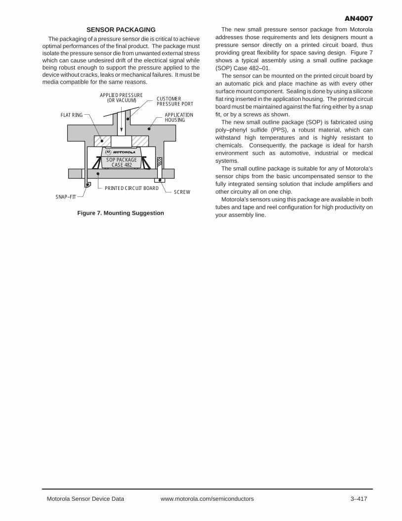
3–417Motorola Sensor Device Data www.motorola.com/semiconductors
SENSOR PACKAGINGThe packaging of a pressure sensor die is critical to achieve
optimal performances of the final product. The package mustisolate the pressure sensor die from unwanted external stresswhich can cause undesired drift of the electrical signal whilebeing robust enough to support the pressure applied to thedevice without cracks, leaks or mechanical failures. It must bemedia compatible for the same reasons.
Figure 7. Mounting Suggestion
CUSTOMER
ÉÉÉÉÉÉÉÉÉÉÉÉ
FLAT RING
APPLIED PRESSURE(OR VACUUM)
PRESSURE PORT
APPLICATIONHOUSING
SCREWSNAP–FIT
PRINTED CIRCUIT BOARD
SOP PACKAGECASE 482
The new small pressure sensor package from Motorolaaddresses those requirements and lets designers mount apressure sensor directly on a printed circuit board, thusproviding great flexibility for space saving design. Figure 7shows a typical assembly using a small outline package(SOP) Case 482–01.
The sensor can be mounted on the printed circuit board byan automatic pick and place machine as with every othersurface mount component. Sealing is done by using a siliconeflat ring inserted in the application housing. The printed circuitboard must be maintained against the flat ring either by a snapfit, or by a screws as shown.
The new small outline package (SOP) is fabricated usingpoly–phenyl sulfide (PPS), a robust material, which canwithstand high temperatures and is highly resistant tochemicals. Consequently, the package is ideal for harshenvironment such as automotive, industrial or medicalsystems.
The small outline package is suitable for any of Motorola’ssensor chips from the basic uncompensated sensor to thefully integrated sensing solution that include amplifiers andother circuitry all on one chip.
Motorola’s sensors using this package are available in bothtubes and tape and reel configuration for high productivity onyour assembly line.

3–418 Motorola Sensor Device Datawww.motorola.com/semiconductors
Prepared by: Memo Romero and Raul FigueroaMotorola Sensor Products DivisionSystems and Applications Engineering
INTRODUCTION
This application note presents a design for a low pressureevaluation board using Motorola MPX2010 series pressuresensors. By providing large gain amplification and allowing forpackage flexibility, this board is intended to serve as adesign-in tool for customers seeking to quickly evaluate thisfamily of pressure sensors.
The MPX2010 family of pressure sensors appeals tocustomers needing to measure small gauge, vacuum, ordifferential pressures at a low cost. However, differentapplications present design–in challenges for these sensors.For very low pressure sensing, large signal amplification isrequired, with gains substantially larger than what is providedin Motorola’s current integrated pressure sensor portfolio. Interms of packaging, customers often need more mechanicalflexibility such as smaller size, dual porting or both. In manycases, customers often lack the engineering resources, timeor expertise to evaluate the sensor. The low-pressureevaluation board, shown in Figure 1, facilitates thedesign-in-process by providing large signal gain and by
providing for different package designs in a relatively smallfootprint.
CIRCUIT DESCRIPTION
For adequate and stable signal gain and output flexibility, atwo–stage differential op-amp circuit with analog or switchoutput is utilized, as shown in Figure 2. The four op-amps arepackaged in a single 14 pin quad package. There are severalfeatures to note about the circuitry.
The first gain stage is accomplished by feeding bothpressure sensor outputs (VS– & VS+) into the non-invertinginputs of operational amplifiers. These op-amps are used inthe standard non-inverting feedback configuration. With thecondition that Resistors R2=R3, and R1=R4 (as closely aspossible), this configuration results in a gain of G1= R4/R3+1. The default gain is 101, but there are provisions for easilychanging this value. The signal V (op-amp Pin 7) is thencalculated as:
V1 = G1*(VS+ – VS–) + Voffset. ….Equation (1)
Figure 1. Low Pressure Evaluation Board
SEMICONDUCTOR APPLICATION NOTE

3–419Motorola Sensor Device Data www.motorola.com/semiconductors
Figure 2. Circuit Schematic
Voffset is the reference voltage for the first op-amp and ispre-set with a voltage divider from the supply voltage. Thisvalue is set to be 6.7 percent of the supply voltage. It isimportant to keep this value relatively small simply because ittoo is amplified by the second gain stage. It is also desirableto have resistors R7 and R8 sufficiently large to reduce powerconsumption.
The second gain stage takes the signal from the first gainstage, V, and feeds it into the non-inverting input of a singleop-amp. This op-amp is also configured with standardnon-inverting feedback, resulting in a gain of G2=R5/R6+1.The default value is set to 2, but can easily be changed.
The signal produced at the output of the second stageamplifier, V (op-amp pin 8) is the fully amplified signal. This iscalculated as
V2 = G2* V1. ….Equation (2)
From this point, there are two possible output typesavailable. One is a simple follower circuit, as shown in Figure3, in which the circuit output, Vout (op-amp pin 14), isessentially a buffered V signal. This analog output option isavailable for applications in which the real time nature of thepressure signal needs to be measured. This option is selectedby connecting jumpers J5 and J6. J4 and J7 are not connectedfor analog output.
The second output choice, a switch output as shown inFigure 4, is accomplished by setting jumpers J4 and J7, andleaving J5 and J6 unconnected. This is appropriate forapplications in which a switching function is desired. In thiscase, the fourth op-amp is configured as a comparator, whichwill invert V2, high or low, depending on whether V2 is largeror smaller than the preset reference signal, set by trim-pot R9.This signal can be used to simulate a real world threshold.
Figure 3. Analog Output Jumper Settings
Figure 4. Switch Output Jumper Settings

3–420 Motorola Sensor Device Datawww.motorola.com/semiconductors
Table 1 shows the jumper settings for both analog andswitches outputs.
Table 1. Output Jumper Settings
ÁÁÁÁÁÁÁÁÁÁ
Output ÁÁÁÁÁÁ
JP4 ÁÁÁÁÁÁ
JP5 ÁÁÁÁÁÁ
JP6 ÁÁÁÁÁÁ
JP7
ÁÁÁÁÁÁÁÁÁÁ
Analog ÁÁÁÁÁÁ
Out ÁÁÁÁÁÁ
In ÁÁÁÁÁÁ
In ÁÁÁÁÁÁ
Out
ÁÁÁÁÁÁÁÁÁÁ
Switch ÁÁÁÁÁÁ
In ÁÁÁÁÁÁ
Out ÁÁÁÁÁÁ
Out ÁÁÁÁÁÁ
In
For the switch output option, it is desirable to apply somehysteresis on the output signal to make it relatively immune topotential noise that may be present in the voltage signal as itreaches and passes the threshold value. This isaccomplished with feedback resistor R10. From basicop-amp theory, it can be shown that the amount of hysteresisis computed as follows:
VH = Vout *[1–(10 / ( R10 + R pot-eff))]
Where:– VH is the output voltage attenuation, due to hystere-
sis, in volts– Vout is the output voltage (railed hi or low)– R10 is the feedback resistor, = 50K– Rpot-eff is the effective potentiometer resistance
VH may vary depending on the particular value of thepotentiometer.
Figure 5a. Output Transition without Hysteresis
Figure 5b. Output Transition with Hysteresis
To take an example, suppose that the supply voltage, Vs is5 volts, and the threshold is set to 60 percent of Vs, or 3 volts.This corresponds to one leg of the 1K potentiometer set to0.4K while the other is set to 0.6K. Thus the effective potresistance is 0.4K // 0.6K = 0.24K.
Therefore,
VH = 5V* [1– (50K/(50K + 0.24K))] = 24 mV.
Under these conditions, V signals passing through thethreshold will not cause Vout to oscillate between Vs andGround as long as noise and signal variations in V are lessthan 24mV during the transition. Figure 5. Illustrates thebenefit of having a hysteresis feedback resistor.
GAIN CUSTOMIZATION
The low-pressure evaluation board comes with defaultgains for both G1 and G2. G1 is factory set at 101, while G2is set to 1. Jumpers JP1, JP2 and JP3 physically connect theresistors that produce these default gains. Three resistorsockets (R11, R41 and R51) are provided in parallel with R1,R4 and R5, respectively. By removing jumpers JP1,JP2 andJP3, and soldering different resistor values in the appropriatesockets, different gain values can be achieved. The limit onthe largest overall gain that can be used is determined byop–amp saturation. Thus if gain values are chosen such thatthe output would be larger than the supply voltage, then theop–amp would saturate, and the pressure would not beaccurately reflected. Table 2 outlines the jumper settings forcustomizing the gain.
Table 2. Resistor and Jumper Settings for GainCustomization
ÁÁÁÁÁÁÁÁ
Gain ÁÁÁÁÁÁÁÁÁÁÁÁÁÁ
Resistors ÁÁÁÁÁÁÁÁÁÁ
Jumpers ÁÁÁÁÁÁÁÁ
Remarks
ÁÁÁÁ
G1ÁÁÁÁÁÁ
G2ÁÁÁÁÁÁ
R11 ÁÁÁÁ
R41ÁÁÁÁÁÁ
R51ÁÁÁÁ
JP1ÁÁÁÁÁÁ
JP2ÁÁÁÁ
JP3ÁÁÁÁÁÁÁÁÁÁ
ÁÁÁÁ
101ÁÁÁÁÁÁÁÁÁ
2ÁÁÁÁÁÁÁÁÁ
noload
ÁÁÁÁÁÁ
noload
ÁÁÁÁÁÁÁÁÁ
noload
ÁÁÁÁÁÁ
InÁÁÁÁÁÁÁÁÁ
InÁÁÁÁÁÁ
InÁÁÁÁÁÁÁÁÁÁÁÁ
Default
ÁÁÁÁÁÁ
UserSet
ÁÁÁÁÁÁÁÁÁ
2ÁÁÁÁÁÁÁÁÁ
loadÁÁÁÁÁÁ
loadÁÁÁÁÁÁÁÁÁ
noload
ÁÁÁÁÁÁ
OutÁÁÁÁÁÁÁÁÁ
OutÁÁÁÁÁÁ
InÁÁÁÁÁÁÁÁÁÁÁÁ
R11=R41
ÁÁÁÁÁÁ
101ÁÁÁÁÁÁÁÁÁ
UserSetÁÁÁÁÁÁÁÁÁ
noloadÁÁÁÁÁÁ
noloadÁÁÁÁÁÁÁÁÁ
loadÁÁÁÁÁÁ
InÁÁÁÁÁÁÁÁÁ
InÁÁÁÁÁÁ
OutÁÁÁÁÁÁÁÁÁÁÁÁÁÁ
ÁÁUserSetÁÁÁÁÁÁ
UserSetÁÁÁÁÁÁ
loadÁÁÁÁ
loadÁÁÁÁÁÁ
loadÁÁÁÁ
OutÁÁÁÁÁÁ
OutÁÁÁÁ
OutÁÁÁÁÁÁÁÁ
R11=R41
DESIGN CONSIDERATIONS
Since the evaluation board is primarily intended forlow–pressure gage and differential applications, large gainvalues can be utilized for pressures less than 1.0 kPa. Forexample if G1 is set to 101, and G2 set to 6, then the total gainis 606.
Inherent in the MPX2010 family of pressure sensors is azero-pressure offset voltage, which can be up to 1 mV. Thisoffset is amplified by the circuit and appears as a DC offset atVout with no pressure applied. The op-amp also has a voltageoffset specification, though for the recommended op-amp thisvalue is small and does not contribute significantly to the Voutoffset.

3–421Motorola Sensor Device Data www.motorola.com/semiconductors
For example, if the evaluation board is being used under thefollowing conditions:
Vs = 3VG1 = 101G2 = 6MPX2010 zero pressure offset = 0.3mV
At this supply voltage, VOFFSET can be calculated to be6.7% x 3V = 0.2V. The voltage V, due simply to the zeropressure sensor offset voltage of 0.3mV, can be calculatedfrom equation (1):
V1 = 0.3mV * 101 + 0.2V = 0.23V
The voltage after the second gain stage comes fromequation (2),
V2 = 6 x 0.23V = 1.38 V.
Therefore, before any pressure is applied to the sensor, a1.38V DC signal will appear at V. Since the supply voltage is3V, the available signal for actual pressure is 1.62 V. With atotal gain of G1 x G2 = 606, the largest raw pressure signal thatcan be accurately measured would be 1.62V/606 = 2.67 mV.For the MPX2010 family operating at Vs = 3V, thiscorresponds to roughly 3.5 kPa.
The board lends itself well to system integration via an A/Dconverter and microprocessor. For particular applications,general knowledge of the expected pressure signal can aid inchoosing the proper customized gain. This will avoid op-ampsaturation and will also ensure that the full-scale output signalis suitable for A/D conversion. To take another example,suppose that a particular application has the followingconstraints:
Supply Voltage, Vs = 5.0 V,(thus VOFFSET = 6.7% x 5 = 0.335 V)
Sensor zero–pressure offset voltage, VZP = 0.3mVExpected Pressure range = 0—2 kPa,
(corresponds to VSENSOR-MAX = 2.5mV @ 5V)Desired maximum output range, V2MAX = 2V
(assume VMIN = 2V, V2MAX = 4V for reasonable A/Dresolution)
By manipulating equations (1) and (2) it can be shown that,
V2MAX = GT x VSENSOR–MAXwhere GT is the total gain, equal to G1G2.
Thus GT = 2V/2.5mV = 800
To find G1 and G2, evaluate V2MIN at the zero pressurecondition.
V2MIN = G2 V1MIN,
But V1MIN = G1 VZP + VOFFSET
Thus V2MIN = GT VZP + G2 VOFFSET
Solving for G2, G2 = (V2MIN – GT VZP)/ VOFFSET
numerically, G2 = (2V — (800x.0003V))/.335V
G2 = 5.2, and G1 = GT /G2 = 152
BOARD LAYOUT & CONTENT
The low-pressure evaluation board has been designedusing standard components. The only item that requirescareful selection is the operation amplifier IC. Because theselected gain may be relatively high as in the previousexample, it is essential that this device have a low offsetvoltage. A device with a typical voltage offset of 35 mV hasbeen selected. Even with a gain of 1500, this will result in a52mV offset. Table 3 is a parts list for the board layout shownin Figure1.
Table 3. Parts List
ÁÁÁÁÁÁÁÁÁ
Ref.ÁÁÁÁÁÁ
Qty.ÁÁÁÁÁÁÁÁÁÁÁÁÁÁÁÁÁÁ
DescriptionÁÁÁÁÁÁÁÁÁ
ValueÁÁÁÁÁÁÁÁÁ
VendorÁÁÁÁÁÁÁÁÁÁÁÁ
Part No.
ÁÁÁÁÁÁ
X1 ÁÁÁÁ
1ÁÁÁÁÁÁÁÁÁÁÁÁ
Pressure Sensor ÁÁÁÁÁÁ10 KpaÁÁÁÁÁÁ
MotorolaÁÁÁÁÁÁÁÁ
MPX2010MPXC2011
ÁÁÁÁÁÁÁÁÁ
C1ÁÁÁÁÁÁ
1ÁÁÁÁÁÁÁÁÁÁÁÁÁÁÁÁÁÁ
Vcc CapÁÁÁÁÁÁÁÁÁ
1 uFÁÁÁÁÁÁÁÁÁ
GenericÁÁÁÁÁÁÁÁÁÁÁÁÁÁÁ
ÁÁÁC2 ÁÁÁÁ
1ÁÁÁÁÁÁÁÁÁÁÁÁ
Op-Amp Cap ÁÁÁÁÁÁ0.1 uF ÁÁÁÁÁÁ
GenericÁÁÁÁÁÁÁÁÁÁÁ
ÁÁÁC3ÁÁÁÁ
1ÁÁÁÁÁÁÁÁÁÁÁÁ
2nd stage capÁÁÁÁÁÁ4700 pFÁÁÁÁÁÁ
GenericÁÁÁÁÁÁÁÁÁÁÁ
ÁÁÁÁÁÁ
D1ÁÁÁÁÁÁ
1ÁÁÁÁÁÁÁÁÁÁÁÁÁÁÁÁÁÁ
LEDÁÁÁÁÁÁÁÁÁ
ÁÁÁÁÁÁÁÁÁ
GenericÁÁÁÁÁÁÁÁÁÁÁÁÁÁÁ
ÁÁÁfor U1ÁÁÁÁ
1ÁÁÁÁÁÁÁÁÁÁÁÁ
Op-Amp socket ÁÁÁÁÁÁÁÁÁÁÁÁ
GenericÁÁÁÁÁÁÁÁÁÁÁ
ÁÁÁÁÁÁ
U1 ÁÁÁÁÁÁ
1ÁÁÁÁÁÁÁÁÁÁÁÁÁÁÁÁÁÁ
Op-Amp ÁÁÁÁÁÁÁÁÁ
ÁÁÁÁÁÁÁÁÁ
AnalogDevices
ÁÁÁÁÁÁÁÁÁÁÁÁ
OP496GP
ÁÁÁÁÁÁ
R1, R4ÁÁÁÁ
2ÁÁÁÁÁÁÁÁÁÁÁÁ
1/4 W Resistor ÁÁÁÁÁÁ100K ÁÁÁÁÁÁ
GenericÁÁÁÁÁÁÁÁÁÁÁ
ÁÁÁÁÁÁ
R2,R3,R5,R6
ÁÁÁÁÁÁ
4ÁÁÁÁÁÁÁÁÁÁÁÁÁÁÁÁÁÁ
1/4 W ResistorÁÁÁÁÁÁÁÁÁ
1KÁÁÁÁÁÁÁÁÁ
GenericÁÁÁÁÁÁÁÁÁÁÁÁÁÁÁ
ÁÁÁR7 ÁÁÁÁ
1ÁÁÁÁÁÁÁÁÁÁÁÁ
1/4 W Resistor ÁÁÁÁÁÁ6.8K ÁÁÁÁÁÁ
GenericÁÁÁÁÁÁÁÁÁÁÁ
ÁÁÁR8ÁÁÁÁ
1ÁÁÁÁÁÁÁÁÁÁÁÁ
1/4 W ResistorÁÁÁÁÁÁ510ÁÁÁÁÁÁ
GenericÁÁÁÁÁÁÁÁÁÁÁ
ÁÁÁÁÁÁ
R9
ÁÁÁÁÁÁ
1
ÁÁÁÁÁÁÁÁÁÁÁÁÁÁÁÁÁÁ
Potentiometer
ÁÁÁÁÁÁÁÁÁ
1K
ÁÁÁÁÁÁÁÁÁ
Bourns
ÁÁÁÁÁÁÁÁÁÁÁÁ
3386P–102
ÁÁÁÁÁÁ
R10 ÁÁÁÁ
1ÁÁÁÁÁÁÁÁÁÁÁÁ
1/4 W Resistor ÁÁÁÁÁÁ51K ÁÁÁÁÁÁ
GenericÁÁÁÁÁÁÁÁÁÁÁ
ÁÁÁR11ÁÁÁÁ
1ÁÁÁÁÁÁÁÁÁÁÁÁ
1/4 W ResistorÁÁÁÁÁÁcustomÁÁÁÁÁÁ
GenericÁÁÁÁÁÁÁÁÁÁÁ
ÁÁÁÁÁÁ
R12ÁÁÁÁÁÁ
1ÁÁÁÁÁÁÁÁÁÁÁÁÁÁÁÁÁÁ
1/4 W ResistorÁÁÁÁÁÁÁÁÁ
2KÁÁÁÁÁÁÁÁÁ
GenericÁÁÁÁÁÁÁÁÁÁÁÁÁÁÁ
ÁÁÁR41 ÁÁÁÁ
1ÁÁÁÁÁÁÁÁÁÁÁÁ
1/4 W Resistor ÁÁÁÁÁÁcustomÁÁÁÁÁÁ
GenericÁÁÁÁÁÁÁÁÁÁÁ
ÁÁÁR51ÁÁÁÁ
1ÁÁÁÁÁÁÁÁÁÁÁÁ
1/4 W ResistorÁÁÁÁÁÁcustomÁÁÁÁÁÁ
GenericÁÁÁÁÁÁÁÁÁÁÁ
ÁÁÁÁÁÁ
JP1 –JP7
ÁÁÁÁÁÁ
7ÁÁÁÁÁÁÁÁÁÁÁÁÁÁÁÁÁÁ
JumperÁÁÁÁÁÁÁÁÁ
ÁÁÁÁÁÁÁÁÁ
GenericÁÁÁÁÁÁÁÁÁÁÁÁÁÁÁ
ÁÁÁJ1ÁÁÁÁ
1ÁÁÁÁÁÁÁÁÁÁÁÁ
3 Pos ConnectorÁÁÁÁÁÁÁÁÁÁÁÁ
PhoenixÁÁÁÁÁÁÁÁ
MKDS1

3–422 Motorola Sensor Device Datawww.motorola.com/semiconductors
Figure 6 illustrates the particular layout chosen for theevaluation board (LED and R12 are not shown). This layoutcan serve as a fully functional stand–alone board or can be thebasis for integration into a system level layout. Through holemounted components have been selected, and this dictatesthe particular footprint dimensions. However, with surfacemount components, this layout can be made significantlysmaller.
Component SideFigure 6a. Board Layout
Figure 6b. Board LayoutBack Side
EVALUATION NOTES:
This board is designed to run from a regulated power sourceor from batteries. Since the pressure sensors are ratio–metric(meaning that the output scales with the applied supplyvoltage), supply voltages ranging from 3V to 10V can be used.The specified op-amp operates well within these values.
In terms of sensor packages, four variations arerecommended. They are the MPX2010D, MPX201DP,MPX2010GP and the MPXC2011DT1. Either of these sensorscan be directly mounted on the board itself or can be remotelymounted and connected to it via wires. The customer canselect the proper package depending on size requirementsand on whether gauge, vacuum or differential pressure will besensed. In particular, the MPXC2011DT1, known as theChipPak sensor, is a very small package and can be used tosense differential and vacuum pressure provided that portsare attached on each side as shown in Figure 1. Note thatMotorola does not provide these ports as standard products.
Since the output signal of the evaluation board can be finedtuned to be a very measurable voltage, interfacing the boardto an A/D, microprocessor, or other circuitry is verystraightforward.
CONCLUSION
The low-pressure evaluation board provides designflexibility in terms of amplification, output type and packaging. Gains ranging from 50 up to 1500 can be easily implementedby simply soldering specific resistors and manipulating a fewjumpers. Jumpers also control the type of output and allow theuser to select analog or switching signals. Two sets of throughhole sensor connections are provided for various pressuresensor packages, and customers are free to remotely mountthe board via wires.
In many applications, such as HVAC systems or medicalrespiratory equipment, quick and effective componentevaluation is critical. The flexible features of this board allowa customer to reduce development time.

3–423Motorola Sensor Device Data www.motorola.com/semiconductors
Package Outline Dimensions
CASE 344–15ISSUE AA
STYLE 1:PIN 1. GROUND
2. + OUTPUT3. + SUPPLY4. – OUTPUT
STYLE 1:PIN 1. GROUND
2. + OUTPUT3. + SUPPLY4. – OUTPUT
CASE 344B–01ISSUE B
SEATINGPLANE
B
N
R
C
J
–T–
D
F
U
HL
PORT #1POSITIVE
PRESSURE
PIN 1
–A–
–Q–
S
K
G4 PL
–P–SQM0.25 (0.010) T
SSM0.13 (0.005) Q ST
1 2 3 4
NOTES:1. DIMENSIONING AND TOLERANCING PER ANSI
Y14.5, 1982.2. CONTROLLING DIMENSION: INCH.
DIM MIN MAX MIN MAXMILLIMETERSINCHES
A 1.145 1.175 29.08 29.85B 0.685 0.715 17.40 18.16C 0.305 0.325 7.75 8.26D 0.016 0.020 0.41 0.51F 0.048 0.064 1.22 1.63G 0.100 BSC 2.54 BSCH 0.182 0.194 4.62 4.93J 0.014 0.016 0.36 0.41K 0.695 0.725 17.65 18.42L 0.290 0.300 7.37 7.62N 0.420 0.440 10.67 11.18P 0.153 0.159 3.89 4.04Q 0.153 0.159 3.89 4.04R 0.230 0.250 5.84 6.35SU 0.910 BSC 23.11 BSC
0.220 0.240 5.59 6.10
(P1)
MAM0.136 (0.005) T
1 2 3 4PIN 1
R
NL
GF
D 4 PL
SEATINGPLANE
–T–
C
M
J
B –A–DIM MIN MAX MIN MAX
MILLIMETERSINCHES
A 0.595 0.630 15.11 16.00B 0.514 0.534 13.06 13.56C 0.200 0.220 5.08 5.59D 0.016 0.020 0.41 0.51F 0.048 0.064 1.22 1.63G 0.100 BSC 2.54 BSCJ 0.014 0.016 0.36 0.40L 0.695 0.725 17.65 18.42M 30 NOM 30 NOMN 0.475 0.495 12.07 12.57R 0.430 0.450 10.92 11.43
NOTES:1. DIMENSIONING AND TOLERANCING PER ASME
Y14.5M, 1994.2. CONTROLLING DIMENSION: INCH.3. DIMENSION –A– IS INCLUSIVE OF THE MOLD
STOP RING. MOLD STOP RING NOT TO EXCEED16.00 (0.630).
DAMBAR TRIM ZONE:
F
THIS IS INCLUDEDWITHIN DIM. “F” 8 PL
12 3
4
Y
Z
Y 0.048 0.052 1.22 1.32Z 0.106 0.118 2.68 3.00

3–424 Motorola Sensor Device Datawww.motorola.com/semiconductors
PACKAGE OUTLINE DIMENSIONS (continued)
STYLE 1:PIN 1. GROUND
2. + OUTPUT3. + SUPPLY4. – OUTPUT
PORT #2
PORT #1
PORT #2VACUUM
SEATINGPLANE
SEATINGPLANE
K
S
WH
LU
FG
D
PORT #1POSITIVE PRESSURE
–Q–
1 2 43PIN 1
4 PL
–P––T– –T– SQM0.25 (0.010) T
SSM0.13 (0.005) Q ST
B
N
JC
V
R
NOTES:1. DIMENSIONING AND TOLERANCING PER ANSI
Y14.5M, 1982.2. CONTROLLING DIMENSION: INCH.
DIM MIN MAX MIN MAXMILLIMETERSINCHES
A 1.145 1.175 29.08 29.85B 0.685 0.715 17.40 18.16C 0.405 0.435 10.29 11.05D 0.016 0.020 0.41 0.51F 0.048 0.064 1.22 1.63G 0.100 BSC 2.54 BSCH 0.182 0.194 4.62 4.93J 0.014 0.016 0.36 0.41K 0.695 0.725 17.65 18.42L 0.290 0.300 7.37 7.62N 0.420 0.440 10.67 11.18P 0.153 0.159 3.89 4.04Q 0.153 0.159 3.89 4.04R 0.063 0.083 1.60 2.11SU 0.910 BSC 23.11 BSCV 0.248 0.278 6.30 7.06W 0.310 0.330 7.87 8.38
–A–
0.220 0.240 5.59 6.10
(P2) (P1)
CASE 344C–01ISSUE B
CASE 344D–01ISSUE B
STYLE 1:PIN 1. GROUND
2. + OUTPUT3. + SUPPLY4. – OUTPUT
NOTES:1. DIMENSIONING AND TOLERANCING PER ANSI
Y14.5, 1982.2. CONTROLLING DIMENSION: INCH.
SEATINGPLANE
B
N
R
C
J
–T–
D
F
U
LHPORT #2
VACUUM POSITIVEPRESSURE
PIN 1
–A–
–Q–
S
K
G4 PL
–P–SQM0.25 (0.010) T
SSM0.13 (0.005) Q ST
DIM MIN MAX MIN MAXMILLIMETERSINCHES
A 1.145 1.175 29.08 29.85B 0.685 0.715 17.40 18.16C 0.305 0.325 7.75 8.26D 0.016 0.020 0.41 0.51F 0.048 0.064 1.22 1.63G 0.100 BSC 2.54 BSCH 0.182 0.194 4.62 4.93J 0.014 0.016 0.36 0.41K 0.695 0.725 17.65 18.42L 0.290 0.300 7.37 7.62N 0.420 0.440 10.67 11.18P 0.153 0.159 3.89 4.04Q 0.153 0.158 3.89 4.04R 0.230 0.250 5.84 6.35SU 0.910 BSC 23.11 BSC
1 2 3 4
0.220 0.240 5.59 6.10
(P2)(P1)

3–425Motorola Sensor Device Data www.motorola.com/semiconductors
PACKAGE OUTLINE DIMENSIONS (continued)
STYLE 1:PIN 1. GROUND
2. + OUTPUT3. + SUPPLY4. – OUTPUT
S
NOTES:1. DIMENSIONING AND TOLERANCING PER ANSI
Y14.5M, 1982.2. CONTROLLING DIMENSION: INCH.
DIM MIN MAX MIN MAXMILLIMETERSINCHES
A 0.690 0.720 17.53 18.28B 0.245 0.255 6.22 6.48C 0.780 0.820 19.81 20.82D 0.016 0.020 0.41 0.51F 0.048 0.064 1.22 1.63G 0.100 BSC 2.54 BSCJ 0.014 0.016 0.36 0.41K 0.345 0.375 8.76 9.53N 0.300 0.310 7.62 7.87R 0.178 0.186 4.52 4.72SV 0.182 0.194 4.62 4.93
BACK SIDEVACUUM
PIN 1
4 PL
PORT #1POSITIVE
PRESSURE
4
SEATINGPLANE
3 2 1
K
A
GF
DMBM0.13 (0.005) T
C
NR
V
J
–B–
–T–
0.220 0.240 5.59 6.10
(P1)(P2)
CASE 344E–01ISSUE B
NOTES:1. DIMENSIONING AND TOLERANCING PER
ANSI Y14.5M, 1982.2. CONTROLLING DIMENSION: INCH.
STYLE 1:PIN 1. GROUND
2. V (+) OUT3. V SUPPLY4. V (–) OUT
E
C
J
V
–T–
PORT #1POSITIVEPRESSURE
PIN 1
4 PLD
–P–
G
K
MQM0.25 (0.010) T
U
A
F
S
N B
SPM0.13 (0.005) Q ST
DIM MIN MAX MIN MAXMILLIMETERSINCHES
A 1.080 1.120 27.43 28.45B 0.740 0.760 18.80 19.30C 0.630 0.650 16.00 16.51D 0.016 0.020 0.41 0.51E 0.160 0.180 4.06 4.57F 0.048 0.064 1.22 1.63G 0.100 BSC 2.54 BSCJ 0.014 0.016 0.36 0.41KN 0.070 0.080 1.78 2.03P 0.150 0.160 3.81 4.06Q 0.150 0.160 3.81 4.06R 0.440 0.460 11.18 11.68S 0.695 0.725 17.65 18.42U 0.840 0.860 21.34 21.84V 0.182 0.194 4.62 4.92
–Q–
R
4 3 2 1
0.220 0.240 5.59 6.10
(P1)
CASE 344F–01ISSUE B

3–426 Motorola Sensor Device Datawww.motorola.com/semiconductors
PACKAGE OUTLINE DIMENSIONS (continued)
CASE 423A–03ISSUE C
DIMA
MIN MAX MIN MAXMILLIMETERS
6.10 6.600.240 0.260
INCHES
B 8.89 9.400.350 0.370C 3.56 3.810.140 0.150D1 0.30 0.510.012 0.020
E 2.24 2.590.088 0.102F 3.12 3.250.123 0.128G 1.14 1.400.045 0.055H 0.94 1.190.037 0.047J 0.18 0.280.007 0.011K 3.05 3.560.120 0.140L 2.41 2.670.095 0.105M 4.19 4.450.165 0.175N 5.66 6.070.223 0.239V 2.67 2.920.105 0.115
AA 2.41 2.720.095 0.107AB 0.38 0.890.015 0.035AC 3.05 4.450.120 0.175AD 2.54 2.920.100 0.115
STYLE 1:PIN 1. VCC
2. +OUT 3. –OUT 4. GROUND
AB
AD
AA
F
AC
BACK VIEW
GD1
V
N
FRONT VIEW
MA
1 2 43
C
L
B
F
K
H
E
J
–T–
END VIEW
D2
DETAIL A
DETAIL A
D2 0.36 0.560.014 0.022
NOTES:1. DIMENSIONING AND TOLERANCING PER ANSI
Y14.5M, 1982.2. CONTROLLING DIMENSION: INCH.

3–427Motorola Sensor Device Data www.motorola.com/semiconductors
PACKAGE OUTLINE DIMENSIONS (continued)
CASE 482–01ISSUE O
DIM MIN MAX MIN MAXMILLIMETERSINCHES
A 10.540.4250.415 10.79B 10.540.4250.415 10.79C 5.380.2300.212 5.84D 0.960.0420.038 1.07G 0.100 BSC 2.54 BSCH 0.002 0.010 0.05 0.25J 0.009 0.011 0.23 0.28K 0.061 0.071 1.55 1.80M 0 7 0 7 N 0.405 0.415 10.29 10.54S 0.709 0.725 18.01 18.41
NOTES:1. DIMENSIONING AND TOLERANCING PER ANSI
Y14.5M, 1982.2. CONTROLLING DIMENSION: INCH.3. DIMENSION A AND B DO NOT INCLUDE MOLD
PROTRUSION.4. MAXIMUM MOLD PROTRUSION 0.15 (0.006).5. ALL VERTICAL SURFACES 5 TYPICAL DRAFT.
S
D
G
8 PL
45
81
N
SBM0.25 (0.010) A ST
–A–
–B–
C
M
J
KPIN 1 IDENTIFIER
H
SEATINGPLANE
–T–
CASE 482A–01ISSUE A
DIM MIN MAX MIN MAXMILLIMETERSINCHES
A 10.540.4250.415 10.79B 10.540.4250.415 10.79C 12.700.5200.500 13.21D 0.960.0420.038 1.07G 0.100 BSC 2.54 BSCH 0.002 0.010 0.05 0.25J 0.009 0.011 0.23 0.28K 0.061 0.071 1.55 1.80M 0 7 0 7 N 0.444 0.448 11.28 11.38S 0.709 0.725 18.01 18.41
NOTES:1. DIMENSIONING AND TOLERANCING PER ANSI
Y14.5M, 1982.2. CONTROLLING DIMENSION: INCH.3. DIMENSION A AND B DO NOT INCLUDE MOLD
PROTRUSION.4. MAXIMUM MOLD PROTRUSION 0.15 (0.006).5. ALL VERTICAL SURFACES 5 TYPICAL DRAFT.
S
D
G
8 PL
45
81
SBM0.25 (0.010) A ST
–A–
–B–
C
M
J
KPIN 1 IDENTIFIER
H
SEATINGPLANE
–T–
N
V
W
V 0.245 0.255 6.22 6.48W 0.115 0.125 2.92 3.17

3–428 Motorola Sensor Device Datawww.motorola.com/semiconductors
PACKAGE OUTLINE DIMENSIONS (continued)
CASE 482B–03ISSUE B
DIM MIN MAX MIN MAXMILLIMETERSINCHES
A 10.540.4250.415 10.79B 10.540.4250.415 10.79C 5.330.2200.210 5.59D 0.660.0340.026 0.864G 0.100 BSC 2.54 BSCJ 0.009 0.011 0.23 0.28K 0.100 0.120 2.54 3.05M 0 15 0 15 N 0.405 0.415 10.29 10.54S 0.540 0.560 13.72 14.22
NOTES:1. DIMENSIONING AND TOLERANCING PER ANSI
Y14.5M, 1982.2. CONTROLLING DIMENSION: INCH.3. DIMENSION A AND B DO NOT INCLUDE MOLD
PROTRUSION.4. MAXIMUM MOLD PROTRUSION 0.15 (0.006).5. ALL VERTICAL SURFACES 5 TYPICAL DRAFT.6. DIMENSION S TO CENTER OF LEAD WHEN
FORMED PARALLEL.
PIN 1 IDENTIFIER
K
SEATINGPLANE–T–
S
G
45
81
–A–
–B–
C
MJ
N
D 8 PL
SBM0.25 (0.010) A ST
DETAIL X
DETAIL X
CASE 482C–03ISSUE B
DIM MIN MAX MIN MAXMILLIMETERSINCHES
A 10.540.4250.415 10.79B 10.540.4250.415 10.79C 12.700.5200.500 13.21D 0.660.0340.026 0.864G 0.100 BSC 2.54 BSCJ 0.009 0.011 0.23 0.28K 0.100 0.120 2.54 3.05M 0 15 0 15 N 0.444 0.448 11.28 11.38S 0.540 0.560 13.72 14.22
NOTES:1. DIMENSIONING AND TOLERANCING PER ANSI
Y14.5M, 1982.2. CONTROLLING DIMENSION: INCH.3. DIMENSION A AND B DO NOT INCLUDE MOLD
PROTRUSION.4. MAXIMUM MOLD PROTRUSION 0.15 (0.006).5. ALL VERTICAL SURFACES 5 TYPICAL DRAFT.6. DIMENSION S TO CENTER OF LEAD WHEN
FORMED PARALLEL.
PIN 1
K
SEATINGPLANE–T–
S
G
45
81
–A–
–B–
C
N
V
W
MJ
V 0.245 0.255 6.22 6.48W 0.115 0.125 2.92 3.17
IDENTIFIER
D 8 PL
SBM0.25 (0.010) A ST
DETAIL X
DETAIL X
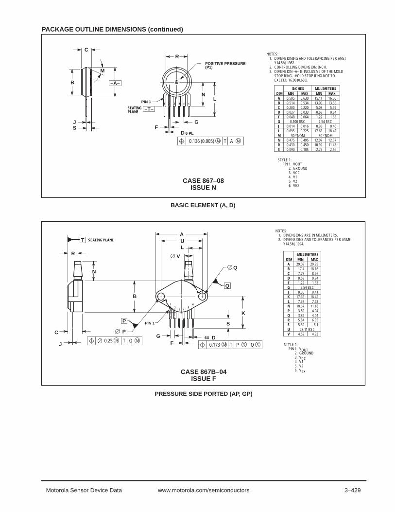
3–429Motorola Sensor Device Data www.motorola.com/semiconductors
PACKAGE OUTLINE DIMENSIONS (continued)
BASIC ELEMENT (A, D)
CASE 867–08ISSUE N
STYLE 1:PIN 1. VOUT
2. GROUND3. VCC4. V15. V26. VEX
PIN 1
FG
NL
RC
B
M
JS
–A–
1 2 3 4 5 6
6 PLD
SEATINGPLANE
–T–
MAM0.136 (0.005) T
DIM MIN MAX MIN MAXMILLIMETERSINCHES
A 0.595 0.630 15.11 16.00B 0.514 0.534 13.06 13.56C 0.200 0.220 5.08 5.59D 0.027 0.033 0.68 0.84F 0.048 0.064 1.22 1.63G 0.100 BSC 2.54 BSCJ 0.014 0.016 0.36 0.40L 0.695 0.725 17.65 18.42M 30 NOM 30 NOMN 0.475 0.495 12.07 12.57R 0.430 0.450 10.92 11.43S 0.090 0.105 2.29 2.66
POSITIVE PRESSURE(P1)
NOTES:1. DIMENSIONING AND TOLERANCING PER ANSI
Y14.5M, 1982.2. CONTROLLING DIMENSION: INCH.3. DIMENSION –A– IS INCLUSIVE OF THE MOLD
STOP RING. MOLD STOP RING NOT TOEXCEED 16.00 (0.630).
PRESSURE SIDE PORTED (AP, GP)
CASE 867B–04ISSUE F
STYLE 1:PIN 1. VOUT
2. GROUND3. VCC4. V15. V26. VEX
SEATING PLANE
R
N
C
J
PIN 1
MQM0.25 T
B
6X DGF
S
K
V
SPM0.173 Q ST
LUA
12
3 45
6
NOTES:1. DIMENSIONS ARE IN MILLIMETERS.2. DIMENSIONS AND TOLERANCES PER ASME
Y14.5M, 1994.
DIM MIN MAXMILLIMETERS
A 29.08 29.85B 17.4 18.16C 7.75 8.26D 0.68 0.84F 1.22 1.63G 2.54 BSCJ 0.36 0.41K 17.65 18.42L 7.37 7.62N 10.67 11.18P 3.89 4.04Q 3.89 4.04R 5.84 6.35S 5.59 6.1U 23.11 BSCV 4.62 4.93
T
P
P
Q
Q

3–430 Motorola Sensor Device Datawww.motorola.com/semiconductors
PACKAGE OUTLINE DIMENSIONS (continued)
PRESSURE AND VACUUM SIDES PORTED (DP)
CASE 867C–05ISSUE F
NOTES:1. DIMENSIONING AND TOLERANCING PER ANSI
Y14.5M, 1982.2. CONTROLLING DIMENSION: INCH.
STYLE 1:PIN 1. VOUT
2. GROUND3. VCC4. V15. V26. VEX
RX
1 2 3 4 5 6
DIM MIN MAX MIN MAXMILLIMETERSINCHES
A 1.145 1.175 29.08 29.85B 0.685 0.715 17.40 18.16C 0.405 0.435 10.29 11.05D 0.027 0.033 0.68 0.84F 0.048 0.064 1.22 1.63G 0.100 BSC 2.54 BSCJ 0.014 0.016 0.36 0.41K 0.695 0.725 17.65 18.42L 0.290 0.300 7.37 7.62N 0.420 0.440 10.67 11.18P 0.153 0.159 3.89 4.04Q 0.153 0.159 3.89 4.04R 0.063 0.083 1.60 2.11SU 0.910 BSC 23.11 BSCV 0.182 0.194 4.62 4.93W 0.310 0.330 7.87 8.38X 0.248 0.278 6.30 7.06
PORT #2 VACUUM (P2)
PORT #1 POSITIVE
PORT #1
PIN 1
PORT #2
POSITIVE
VACUUM
PRESSURE
SEATINGPLANE
SEATINGPLANE –T– –T–
P
G
C
J
N
B
FD
WV
LU
6 PL
S
K
–Q–
–A–MQM0.25 (0.010) T
MAM0.13 (0.005)
PRESSURE (P1)
0.220 0.240 5.59 6.10
(P1)
(P2)
PRESSURE SIDE PORTED (AS, GS)
CASE 867E–03ISSUE D
NOTES:1. DIMENSIONING AND TOLERANCING PER ANSI
Y14.5M, 1982.2. CONTROLLING DIMENSION: INCH.
STYLE 1:PIN 1. VOUT
2. GROUND3. VCC4. V15. V26. VEX
A
6 5 4 3 2 1
C
K
N E
–B–
PORT #1POSITIVE
PRESSURE
J
–T–
S
GF
D 6 PL
PIN 1
MBM0.13 (0.005) T
DIM MIN MAX MIN MAXMILLIMETERSINCHES
A 0.690 17.53 18.28B 0.245 0.255 6.22 6.48C 0.780 0.820 19.81 20.82D 0.027 0.033 0.69 0.84E 0.178 0.186 4.52 4.72F 0.048 0.064 1.22 1.63G 0.100 BSC 2.54 BSCJ 0.014 0.016 0.36 0.41K 0.345 0.375 8.76 9.53N 0.300 0.310 7.62 7.87S 0.220 0.240 5.59 6.10
0.720V
V 0.182 0.194 4.62 4.93
(P1)

3–431Motorola Sensor Device Data www.motorola.com/semiconductors
PACKAGE OUTLINE DIMENSIONS (continued)
PRESSURE SIDE PORTED (ASX, GSX)
CASE 867F–03ISSUE D
STYLE 1:PIN 1. VOUT
2. GROUND3. VCC4. V15. V26. VEX
NOTES:1. DIMENSIONING AND TOLERANCING
PER ANSI Y14.5M, 1982.2. CONTROLLING DIMENSION: INCH.
C
E
V
J
PORT #1POSITIVE
PRESSURE
–T–
–P–MQM0.25 (0.010) T
D
F
G6 PL
K
S
PIN 1
U
A
R
B
–Q–
N
SPM0.13 (0.005) Q ST
6 5 4 3 2 1
DIM MIN MAX MIN MAXMILLIMETERSINCHES
A 1.080 1.120 27.43 28.45B 0.740 0.760 18.80 19.30C 0.630 0.650 16.00 16.51D 0.027 0.033 0.68 0.84E 0.160 0.180 4.06 4.57F 0.048 0.064 1.22 1.63G 0.100 BSC 2.54 BSCJ 0.014 0.016 0.36 0.41KN 0.070 0.080 1.78 2.03P 0.150 0.160 3.81 4.06Q 0.150 0.160 3.81 4.06R 0.440 0.460 11.18 11.68S 0.695 0.725 17.65 18.42U 0.840 0.860 21.34 21.84V 0.182 0.194 4.62 4.93
0.220 0.240 5.59 6.10
(P1)

3–432 Motorola Sensor Device Datawww.motorola.com/semiconductors
PACKAGE OUTLINE DIMENSIONS (continued)
CASE 1317–03ISSUE B
0.025
0.298
0.050
AM0.004 BC
0.165
0.280A B
C
NOTES:1. ALL DIMENSIONS ARE IN INCHES.2. DIMENSIONING AND TOLERANCING PER ASME
Y14.5M–1994.3. DIMENSIONS DO NOT INCLUDE MOLD FLASH OR
PROTRUSIONS. MOLD FLASH OR PROTRUSIONSSHALL NOT EXCEED .006 INCHES PER SIDE.
4. ALL VERTICAL SURFACES TO BE 5° MAXIMUM.5. DIMENSION DOES NOT INCLUDE DAMBAR
PROTRUSION. ALLOWABLE DAMBARPROTRUSION SHALL BE .008 INCHES MAXIMUM.
0.004
A0.006 BC
GAGEPLANE
DETAIL E
0.0230.010
.010
8X 0.014
2X
DETAIL ESEATINGPLANE
0.019
0.300
0.2800.300
0.4000.420
3
5
0.278
0.145
0.0020.013
°100°
3

3–433Motorola Sensor Device Data www.motorola.com/semiconductors
PACKAGE OUTLINE DIMENSIONS (continued)
CASE 1317A–01ISSUE A
0.025
0.130
0.050
AM0.004 BC
0.390
0.325A B
C
NOTES:1. ALL DIMENSIONS ARE IN INCHES.2. DIMENSIONING AND TOLERANCING PER ASME
Y14.5M–1994.3. DIMENSIONS DO NOT INCLUDE MOLD FLASH OR
PROTRUSIONS. MOLD FLASH OR PROTRUSIONSSHALL NOT EXCEED .006 INCHES PER SIDE.
4. ALL VERTICAL SURFACES TO BE 5° MAXIMUM.5. DIMENSION DOES NOT INCLUDE DAMBAR
PROTRUSION. ALLOWABLE DAMBARPROTRUSION SHALL BE .008 INCHES MAXIMUM.
0.004
A0.006 BC
GAGEPLANE
DETAIL E
0.0480.010
.0148X 0.014
2X
DETAIL ESEATINGPLANE
0.018
0.345
0.3250.345
0.4000.420
5
0.110
0.370
0.0020.038
°100°
0.2000.180
0.280A B
0.300
0.2800.300
3
3
BOTTOM VIEW

3–434 Motorola Sensor Device Datawww.motorola.com/semiconductors
PACKAGE OUTLINE DIMENSIONS (continued)
CASE 1320–02ISSUE A
DIM MIN MAXINCHES
A .155 .165A1 .002 .010b .014 .018b1 .120 .130D .245 .255E .475 .485
ee/2L .038 .048
E1 .325 .335
0 7
.025 BSC
.050 BSC
θ ° °
NOTES:1. DIMENSIONS ARE IN INCHES.2. INTERPRET DIMENSIONS AND TOLERANCES PER
ASME Y14.5M–1994.3. DIMENSIONS ”D” AND ”E1” DO NOT INCLUDE
MOLD FLASH OR PROTRUSION. MOLD FLASH ORPROTRUSION SHALL NOT EXCEED .006” PERSIDE.
4. ALL VERTICAL SURFACES TO BE 5° MAXIMUM.5. DIMENSIONS ”b” DOES NOT INCLUDE DAMBAR
PROTRUSION. ALLOWABLE DAMBARPROTRUSION SHALL BE .008 MAXIMUM.
b1
E
e/2
e
AM0.004 BC
A0.006 BC
4X b
2X
AM0.004 BC
E1
A
C
0.004
DETAIL E
SEATINGPLANE
GAGEPLANE
DETAIL E
LA1 θ
.014
B DA
PIN 1
PIN 4
STYLE 1:PIN 1. GND
2. +Vout 3. Vs 4. –Vout

3–435Motorola Sensor Device Data www.motorola.com/semiconductors
PACKAGE OUTLINE DIMENSIONS (continued)
CASE 1320A–02ISSUE O
DIM MIN MAXINCHES
A .377 .397A1 .002 .010b .014 .018b1 .120 .130D .245 .255E .475 .485
ee/2L .013 .023
E1 .325 .335
0 7
.025 BSC
.050 BSC
θ ° °
NOTES:1. DIMENSIONS ARE IN INCHES.2. INTERPRET DIMENSIONS AND TOLERANCES PER
ASME Y14.5M–1994.3. DIMENSIONS ”D” AND ”E1” DO NOT INCLUDE
MOLD FLASH OR PROTRUSION. MOLD FLASH ORPROTRUSION SHALL NOT EXCEED .006” PERSIDE.
4. ALL VERTICAL SURFACES TO BE 5° MAXIMUM.5. DIMENSIONS ”b” DOES NOT INCLUDE DAMBAR
PROTRUSION. ALLOWABLE DAMBARPROTRUSION SHALL BE .008 MAXIMUM.
b1
E
e/2
e
AM0.004 BC
A0.006 BC
4X b
2X
AM0.004 BC
E1
A
C
0.004
DETAIL E
SEATINGPLANE
GAGEPLANE
DETAIL E
LA1 θ
.014
B DA
M .283 .293N .363 .373P .107 .117S .192 .202
N
S
P

3–436 Motorola Sensor Device Datawww.motorola.com/semiconductors
PACKAGE OUTLINE DIMENSIONS (continued)
CASE 1351–01ISSUE O
D
E
e/2
N
e
AM0.004 (0.1) BC
A
E1
A
B
C
0.004 (0.1)
A0.006 (0.15) BC
8X b
2 PLACES 4 TIPS
DETAIL GSEATINGPLANE
8XP
1
4
8
5
NOTES:1. CONTROLLING DIMENSION: INCH.2. INTERPRET DIMENSIONS AND TOLERANCES PER
ASME Y14.5M–1994.3. DIMENSIONS ”D” AND ”E1” DO NOT INCLUDE
MOLD FLASH OR PROTRUSIONS. MOLD FLASH ORPROTRUSIONS SHALL NOT EXCEED 0.006 (0.152)PER SIDE.
4. DIMENSION ”b” DOES NOT INCLUDE DAMBARPROTRUSION. ALLOWABLE DAMBARPROTRUSION SHALL BE 0.008 (0.203) MAXIMUM.
DIMA
MIN MAX MIN MAXMILLIMETERS
0.370 0.390 9.39 9.91
INCHES
A1 0.002 0.010 0.05 0.25b 0.038 0.042 0.96 1.07D 0.465 0.485 11.81 12.32E 0.680 0.700 17.27 17.78E1 0.465 0.485 11.81 12.32e
M 0.270 0.290 6.86 7.37N 0.160 0.180 4.06 4.57P 0.009 0.011 0.23 0.28T 0.110 0.130 2.79 3.30
0.100 BSC 2.54 BSCF 0.240 0.260 6.10 6.60K 0.115 0.135 2.92 3.43L 0.040 0.060 1.02 1.52
F
K
M
T∅
GAGE
DETAIL G
L A1θ.014 (0.35)
PLANE
0 7 0 7 ° ° ° °θ
STYLE 1:PIN 1. GND
2. +Vout 3. Vs 4. –Vout 5. N/C 6. N/C 7. N/C 8. N/C
STYLE 2:PIN 1. N/C
2. Vs 3. GND 4. Vout 5. N/C 6. N/C 7. N/C 8. N/C

3–437Motorola Sensor Device Data www.motorola.com/semiconductors
PACKAGE OUTLINE DIMENSIONS (continued)
CASE 1368–01ISSUE O
D
E
e/2
N
e
AM0.004 (0.1) BC
A
E1
A
B
C
0.004 (0.1)
A0.006 (0.15) BC
8X b
2 PLACES 4 TIPS
DETAIL GSEATINGPLANE
8XP
1
4
8
5
NOTES:1. CONTROLLING DIMENSION: INCH.2. INTERPRET DIMENSIONS AND TOLERANCES PER
ASME Y14.5M–1994.3. DIMENSIONS ”D” AND ”E1” DO NOT INCLUDE
MOLD FLASH OR PROTRUSIONS. MOLD FLASH ORPROTRUSIONS SHALL NOT EXCEED 0.006 (0.152)PER SIDE.
4. DIMENSION ”b” DOES NOT INCLUDE DAMBARPROTRUSION. ALLOWABLE DAMBARPROTRUSION SHALL BE 0.008 (0.203) MAXIMUM.
DIMA
MIN MAX MIN MAXMILLIMETERS
0.280 0.300 7.11 7.62
INCHES
A1 0.002 0.010 0.05 0.25b 0.038 0.042 0.96 1.07D 0.465 0.485 11.81 12.32EE1 0.465 0.485 11.81 12.32e
M 0.035 0.055 1.90 2.41N 0.075 0.095 0.89 1.39P 0.009 0.011 0.23 0.28
R 0.405 0.415 10.28 10.54
0.100 BSC 2.54 BSCF 0.240 0.260 6.10 6.60K 0.115 0.135 2.92 3.43L 0.040 0.060 1.02 1.52
F
K
M
R∅
GAGE
DETAIL G
L A1θ.014 (0.35)
PLANE
0 7 0 7 ° ° ° °θ
STYLE 1:PIN 1. GND
2. +Vout 3. Vs 4. –Vout 5. N/C 6. N/C 7. N/C 8. N/C
STYLE 2:PIN 1. N/C
2. Vs 3. GND 4. Vout 5. N/C 6. N/C 7. N/C 8. N/C
T∅
T 0.110 0.130 2.79 3.30
0.690 BSC 17.52 BSC

3–438 Motorola Sensor Device Datawww.motorola.com/semiconductors
PACKAGE OUTLINE DIMENSIONS (continued)
CASE 1369–01ISSUE O
D
E
e/2
N
e
AM0.004 (0.1) BC
A
E1
A
B
C
0.004 (0.1)
A0.008 (0.20) BC
8X b
2 PLACES 4 TIPS
DETAIL GSEATINGPLANE
8XP
1
4
8
5
NOTES:1. CONTROLLING DIMENSION: INCH.2. INTERPRET DIMENSIONS AND TOLERANCES PER
ASME Y14.5M–1994.3. DIMENSIONS ”D” AND ”E1” DO NOT INCLUDE
MOLD FLASH OR PROTRUSIONS. MOLD FLASH ORPROTRUSIONS SHALL NOT EXCEED 0.006 (0.152)PER SIDE.
4. DIMENSION ”b” DOES NOT INCLUDE DAMBARPROTRUSION. ALLOWABLE DAMBARPROTRUSION SHALL BE 0.008 (0.203) MAXIMUM.
DIMA
MIN MAX MIN MAXMILLIMETERS
0.300 0.330 7.11 7.62
INCHES
A1 0.002 0.010 0.05 0.25b 0.038 0.042 0.96 1.07D 0.465 0.485 11.81 12.32EE1 0.465 0.485 11.81 12.32e
M 0.270 0.290 6.86 7.36N 0.080 0.090 2.03 2.28P 0.009 0.011 0.23 0.28T 0.115 0.125 2.92 3.17
0.100 BSC 2.54 BSCF 0.245 0.255 6.22 6.47K 0.120 0.130 3.05 3.30L 0.061 0.071 1.55 1.80
F
K
M
GAGE
DETAIL G
L A1θ.014 (0.35)
PLANE
0 7 0 7 ° ° ° °θ
T∅
0.717 BSC 18.21 BSC

3–439Motorola Sensor Device Data www.motorola.com/semiconductors
Reference Tables
FLOW EQUIVALENTS1 Cu. Ft./Hr. 1 Cu. Ft./Min. 1 CC/Min. 1 CC/Hr.
0.01660.471928.316471.947283170.12477.481
Cu. Ft./MinLPMLPHCC/Min.CC/Hr.Gal/Min.Gal/Hr.
6028.3161699283171,699,0117.481448.831
Cu. Ft./MinLPMLPHCC/Min.CC/Hr.Gal/Min.Gal/Hr.
600.0000350.00210.0010.060.000260.0159
CC/Hr.Cu. Ft./MinCu. Ft./Hr.LPMLPHGal/Min.Gal/Hr.
0.01670.00000050.000030.0000170.0010.0000040.00026
CC/Min.Cu. Ft./Min.Cu. Ft./Hr.LPMLPHGal/Min.Gal/Hr.
1 LPM 1 LPH 1 Gal/Min. 1 Gal/Hr.
LPHCu. Ft./Min.Cu. Ft./Hr.CC/Min.CC/Hr.Gal/Min.Gal/Hr.
600.0352.1189100060,0020.26415.851
0.01660.000590.03516.66710000.0040.264
LPMCu. Ft./Min.Cu. Ft./Hr.CC/Min.CC/Hr.Gal/Min.Gal/Hr.
600.13378.0213.785227.1183,785.412227,125
Gal/Hr.Cu. Ft./Min.Cu. Ft./Hr.LPMLPHCC/Min.CC/Hr.
0.01670.0020.13370.0633.78563.0693785
Gal/Min.Cu. Ft./Min.Cu. Ft./Hr.LPMLPHCC/Min.CC/Hr.
Airspeed
KnotsInches ofMercury Knots
Inches ofMercury
860880100110120130140150175200225250275300325350375
0.17270.30750.48140.58320.69500.81680.94881.09101.49181.95892.49433.10023.77924.53435.36876.28597.2900
8,4008,4258,4508,4758,5008,5258,5508,5758,6008,6508,7008,7508,8008,8508,9001,000
88.385089.575810.867512.265413.775615.404517.159019.046521.074925.589330.764236.566242.937849.842357.255473.5454
Altitude(Feet)
EquivalentPressure(inches ofMercury)
Altitude(Feet)
EquivalentPressure(inches ofMercury)
–1,000–900
0500
1,0001,5002,0003,0004,0006,0008,00010,00012,000
31.018530.907329.921329.384628.855728.334527.821026.816725.841823.978222.225020.577019.0294
14,00016,00018,00020,00022,00025,00030,00035,00040,00045,00049,90050,000
17.577416.216414.942113.750112.636311.10358.885447.040625.538024.354883.441123.42466
(EST)

3–440 Motorola Sensor Device Datawww.motorola.com/semiconductors
Reference Tables (continued)
Conversion Table for Common Units of Pressure
kiloPascals mm Hg millibars inches H 2O PSI
1 atm 101.325 760.000 1013.25 406.795 14.6960
1 kiloPascal 1.00000 7.50062 10.0000 4.01475 0.145038
1 mm Hg 0.133322 1.00000 1.33322 0.535257 0.0193368
1 millibar 0.100000 0.750062 1.00000 0.401475 0.0145038
1 inch H2O 0.249081 1.86826 2.49081 1.00000 0.0361
1 PSI 6.89473 51.7148 68.9473 27.6807 1.00000
1 hectoPascal 0.100000 0.75006 1.00000 0.401475 0.0145038
1 cm H2O 0.09806 0.7355 9.8 x 10⁻⁷ 0.3937 0.014223
Quick Conversion Chart for Common Units of Pressure
kiloPascals
inches H2O
millibars
mm Hg
PSI
0 20 40 60 80 100 120 140 160 180 200
0 100 200 300 400 500 600 700 800
0 200 400 600 800 1000 1200 1400 1600 1800 2000
0 200 400 600 800 1000 1200 1400 1600
0 5 10 15 20 25 30

3–441Motorola Sensor Device Data www.motorola.com/semiconductors
Mounting and Handling Suggestions
Custom Port Adaptor Installation Techniques
The Motorola MPX silicon pressure sensor is available in abasic chip carrier cell which is adaptable for attachmentto customer specific housings/ports (Case 344 for 4-pindevices and Case 867 for 6-pin devices). The basic cell haschamfered shoulders on both sides which will accept an O-ring such as Parker Seal’s silicone O-ring(p/n#2-015-S-469-40). Refer to Figure 1 for the recommendedO-ring to sensor cell interface dimensions.
The sensor cell may also be glued directly to a customhousing or port using many commercial grade epoxies or RTVadhesives which adhere to grade Valox 420, reinforcedpolyester resin plastic polysulfone (MPX2040D only). Theepoxy should be dispensed in a continuous bead around thecell-to-port interface shoulder. Refer to Figure 2. Care must betaken to avoid gaps or voids in the adhesive bead to helpensure that a complete seal is made when the cell is joined tothe port. After cure, a simple test for gross leaks should beperformed to ensure the integrity of the cell to port bond.Submerging the device in water for 5 seconds with full ratedpressure applied to the port nozzle and checking for airbubbles will provide a good indication. Be sure device isthoroughly dried after this test.
Figure 2.
ADHESIVE BEAD
Standard Port Attach Connection
Motorola also offers standard port options designed toaccept readily available silicone, vinyl, nylon or polyethylenetubing for the pressure connection. The inside dimension ofthe tubing selected should provide a snug fit over the portnozzle. Dimensions of the ports may be found in the caseoutline drawings. Installation and removal of tubing from theport nozzle must be parallel to the nozzle to avoid undue stresswhich may break the nozzle from the port base. Whethersensors are used with Motorola’s standard ports or customerspecific housings, care must be taken to ensure that force isuniformly distributed to the package or offset errors may beinduced.
Electrical Connection
The MPX series pressure sensor is designed to be installedon a printed circuit board (standard 0.100″ lead spacing) or toaccept an appropriate connector if installed on a baseplate.The leads of the sensor may be formed at right angles forassembly to the circuit board, but one must ensure that properleadform techniques and tools are employed. Hand or“needlenose” pliers should never be used for leadformingunless they are specifically designed for that purpose.Industrial leadform tooling is available from various compan-ies including Janesville Tool & Manufacturing (608-868-4925).Refer to Figure 3 for the recommended leadform technique. Itis also important that once the leads are formed, they shouldnot be straightened and reformed without expecting reduceddurability. The recommended connector for off-circuit boardapplications may be supplied by JST Corp. (1-800-292-4243)in Mount Prospect, IL. The part numbers for the housing andpins are:
4 Pin Housing: SMP-04V-BC6 Pin Housing: SMP-06V-BCPin: SHF-01T-0.8SSThe crimp tool part number is: YC12.
Figure 1.
.114 .047 0
.125
.075
.037R
0
.021
.210″
CELL
Figure 3. Leadforming
TOP CLAMP AREA
BOTTOM CLAMP AREA
Leads should be securely clamped topand bottom in the area between theplastic body and the form being surethat no stress is being put on plasticbody. The area between dotted linesrepresents surfaces to be clamped.

3–442 Motorola Sensor Device Datawww.motorola.com/semiconductors
Standard Warranty Clause
Seller warrants that its products sold hereunder will at the time of shipment be free from defects inmaterial and workmanship, and will conform to Seller’s approved specifications. If products are notas warranted, Seller shall, at its option and as Buyer’s exclusive remedy, either refund the purchaseprice, or repair, or replace the product, provided proof of purchase and written notice ofnonconformance are received within the applicable periods noted below and provided saidnonconforming products are, with Seller’s written authorization, returned in protected shippingcontainers FOB Seller’s plant within thirty (30) days after expiration of the warranty period unlessotherwise specified herein. If product does not conform to this warranty, Seller will pay for thereasonable cost of transporting the goods to and from Seller’s plant. This warranty shall not applyto any products Seller determines have been, by Buyer or otherwise, subjected to improper testing,or have been the subject of mishandling or misuse.
THIS WARRANTY EXTENDS TO BUYER ONLY AND MAY BE INVOKED BY BUYER ONLY FORITS CUSTOMERS. SELLER WILL NOT ACCEPT WARRANTY RETURNS DIRECTLY FROMBUYER’S CUSTOMERS OR USERS OF BUYER’S PRODUCTS. THIS WARRANTY IS IN LIEUOF ALL OTHER WARRANTIES WHETHER EXPRESS, IMPLIED OR STATUTORY INCLUDINGIMPLIED WARRANTIES OF MERCHANTABILITY OR FITNESS FOR A PARTICULAR PURPOSE.
Seller’s warranty shall not be enlarged, and no obligation or liability shall arise out of Seller’srendering of technical advice and/or assistance.
A. Time periods, products, exceptions and other restrictions applicable to the above warranty are:
(1) Unless otherwise stated herein, products are warranted for a period of one (1) year from dateof shipment.
(2) Device Chips/Wafers. Seller warrants that device chips or wafers have, at shipment, beensubjected to electrical test/probe and visual inspection. Warranty shall apply to productsreturned to Seller within ninety (90) days from date of shipment. This warranty shall not applyto any chips or wafers improperly removed from their original shipping container and/orsubjected to testing or operational procedures not approved by Seller in writing.
B. Development products and Licensed Programs are licensed on an “AS IS” basis. IN NO EVENTSHALL SELLER BE LIABLE FOR ANY INCIDENTAL OR CONSEQUENTIAL DAMAGES.

3–443Motorola Sensor Device Data www.motorola.com/semiconductors
Glossary of Terms
Absolute Pressure Sensor A sensor which measures input pressure in relation to a zero pressure (a total vacuum on one side ofthe diaphragm) reference.
Analog Output An electrical output from a sensor that changes proportionately with any change in input pressure.
Accuracy — also seePressure Error
A comparison of the actual output signal of a device to the true value of the input pressure. The variouserrors (such as linearity, hysteresis, repeatability and temperature shift) attributing to the accuracy ofa device are usually expressed as a percent of full scale output (FSO).
Altimetric PressureTransducer
A barometric pressure transducer used to determine altitude from the pressure-altitude profile.
Barometric PressureTransducer
An absolute pressure sensor that measures the local ambient atmospheric pressure.
Burst Pressure The maximum pressure that can be applied to a transducer without rupture of either the sensing ele-ment or transducer case.
Calibration A process of modifying sensor output to improve output accuracy.
Chip A die (unpackaged semiconductor device) cut from a silicon wafer, incorporating semiconductor cir-cuit elements such as resistors, diodes, transistors, and/or capacitors.
Compensation Added circuitry or materials designed to counteract known sources of error.
Diaphragm The membrane of material that remains after etching a cavity into the silicon sensing chip. Changesin input pressure cause the diaphragm to deflect.
Differential Pressure Sensor A sensor which is designed to accept simultaneously two independent pressure sources. The outputis proportional to the pressure difference between the two sources.
Diffusion A thermochemical process whereby controlled impurities are introduced into the silicon to define thepiezoresistor. Compared to ion implantation, it has two major disadvantages: 1) the maximum impuri-ty concentration occurs at the surface of the silicon rendering it subject to surface contamination,and making it nearly impossible to produce buried piezoresistors; 2) control over impurity concentra-tions and levels is about one thousand times poorer than obtained with ion implantation.
Drift An undesired change in output over a period of time, with constant input pressure applied.
End Point Straight Line Fit Motorola’s method of defining linearity. The maximum deviation of any data point on a sensor outputcurve from a straight line drawn between the end data points on that output curve.
Error The algebraic difference between the indicated value and the true value of the input pressure.Usually expressed in percent of full scale span, sometimes expressed in percent of the sensor outputreading.
Error Band The band of maximum deviations of the output values from a specified reference line or curve dueto those causes attributable to the sensor. Usually expressed as “± % of full scale output.” Theerror band should be specified as applicable over at least two calibration cycles, so as to includerepeatability, and verified accordingly.
Excitation Voltage (Current) —see Supply Voltage (Current)
The external electrical voltage and/or current applied to a sensor for its proper operation (often referredto as the supply circuit or voltage). Motorola specifies constant voltage operation only.
Full Scale Output The output at full scale pressure at a specified supply voltage. This signal is the sum of the offset signalplus the full scale span.
Full Scale Span The change in output over the operating pressure range at a specified supply voltage. The SPAN ofa device is the output voltage variation given between zero differential pressure and any givenpressure. FULL SCALE SPAN is the output variation between zero differential pressure and when themaximum recommended operating pressure is applied.
Hysteresis — also see PressureHysteresis and TemperatureHysteresis
HYSTERESIS refers to a transducer’s ability to reproduce the same output for the same input,regardless of whether the input is increasing or decreasing. PRESSURE HYSTERESIS is measuredat a constant temperature while TEMPERATURE HYSTERESIS is measured at a constant pressurein the operating pressure range.

3–444 Motorola Sensor Device Datawww.motorola.com/semiconductors
Glossary of Terms (continued)
Input Impedance (Resistance) The impedance (resistance) measured between the positive and negative (ground) input terminalsat a specified frequency with the output terminals open. For Motorola X-ducer, this is a resistancemeasurement only.
Ion Implantation A process whereby impurity ions are accelerated to a specific energy level and impinged upon thesilicon wafer. The energy level determines the depth to which the impurity ions penetrate the silicon.Impingement time determines the impurity concentration. Thus, it is possible to independentlycontrol these parameters, and buried piezoresistors are easily produced. Ion implantation isincreasingly used throughout the semiconductor industry to provide a variety of products withimproved performance over those produced by diffusion.
Laser Trimming (Automated) A method for adjusting the value of thin film resistors using a computer-controlled laser system.
Leakage Rate The rate at which a fluid is permitted or determined to leak through a seal. The type of fluid, thedifferential pressure across the seal, the direction of leakage, and the location of the seal must bespecified.
Linearity Error The maximum deviation of the output from a straight line relationship with pressure over theoperating pressure range, the type of straight line relationship (end point, least squareapproximation, etc.) should be specified.
Load Impedance The impedance presented to the output terminals of a sensor by the associated external circuitry.
Null The condition when the pressure on each side of the sensing diaphragm is equal.
Null Offset The electrical output present, when the pressure sensor is at null.
Null Temperature Shift The change in null output value due to a change in temperature.
Null Output See ZERO PRESSURE OFFSET
Offset See ZERO PRESSURE OFFSET
Operating Pressure Range The range of pressures between minimum and maximum pressures at which the output will meetthe specified operating characteristics.
Operating Temperature Range The range of temperature between minimum and maximum temperature at which the output willmeet the specified operating characteristics.
Output Impedance The impedance measured between the positive and negative (ground) output terminals at a speci-fied frequency with the input open.
Overpressure The maximum specified pressure which may be applied to the sensing element of a sensor withoutcausing a permanent change in the output characteristics.
Piezoresistance A resistive element that changes resistance relative to the applied stress it experiences (e.g., straingauge).
Pressure Error The maximum difference between the true pressure and the pressure inferred from the output forany pressure in the operating pressure range.
Pressure Hysteresis The difference in the output at any given pressure in the operating pressure range when thispressure is approached from the minimum operating pressure and when approached from themaximum operating pressure at room temperature.
Pressure Range — also seeOperating Pressure Range
The pressure limits over which the pressure sensor is calibrated or specified.
Pressure Sensor A device that converts an input pressure into an electrical output.
Proof Pressure See OVERPRESSURE
Ratiometric Ratiometricity refers to the ability of the transducer to maintain a constant sensitivity, at a constantpressure, over a range of supply voltage values.
Ratiometric(Ratiometricity Error)
At a given supply voltage, sensor output is a proportion of that supply voltage. Ratiometricity erroris the change in this proportion resulting from any change to the supply voltage. Usually expressedas a percent of full scale output.

3–445Motorola Sensor Device Data www.motorola.com/semiconductors
Glossary of Terms (continued)
Range See OPERATING PRESSURE RANGE
Repeatability The maximum change in output under fixed operating conditions over a specified period of time.
Resolution The maximum change in pressure required to give a specified change in the output.
Response Time The time required for the incremental change in the output to go from 10% to 90% of its final valuewhen subjected to a specified step change in pressure.
Room Conditions Ambient environmental conditions under which sensors most commonly operate.
Sensing Element That part of a sensor which responds directly to changes in input pressure.
Sensitivity The change in output per unit change in pressure for a specified supply voltage or current.
Sensitivity Shift A change in sensitivity resulting from an environmental change such as temperature.
Stability The maximum difference in the output at any pressure in the operating pressure range when thispressure is applied consecutively under the same conditions and from the same direction.
Storage Temperature Range The range of temperature between minimum and maximum which can be applied without causingthe sensor to fail to meet the specified operating characteristics.
Strain Gauge A sensing device providing a change in electrical resistance proportional to the level of appliedstress.
Supply Voltage (Current) The voltage (current) applied to the positive and negative (ground) input terminals.
Temperature Coefficient ofFull Scale Span
The percent change in full scale span per unit change in temperature relative to the full scale spanat a specified temperature.
Temperature Coefficient ofResistance
The percent change in the DC input impedance per unit change in temperature relative to the DCinput impedance at a specified temperature.
Temperature Error The maximum change in output at any pressure in the operating pressure range when the tempera-ture is changed over a specified temperature range.
Temperature Hysteresis The difference in output at any temperature in the operating temperature range when the tempera-ture is approached from the minimum operating temperature and when approached from themaximum operating temperature with zero pressure applied.
Thermal Offset Shift See TEMPERATURE COEFFICIENT OF OFFSET
Thermal Span Shift See TEMPERATURE COEFFICIENT OF FULL SCALE SPAN
Thermal Zero Shift See TEMPERATURE COEFFICIENT OF OFFSET
Thin Film A technology using vacuum deposition of conductors and dielectric materials onto a substrate(frequently silicon) to form an electrical circuit.
Vacuum A perfect vacuum is the absence of gaseous fluid.
Zero Pressure Offset The output at zero pressure (absolute or differential, depending on the device type) for a speci-fied supply voltage or current.

3–446 Motorola Sensor Device Datawww.motorola.com/semiconductors
Symbols, Terms and Definitions
The following are the most commonly used letter symbols, terms and definitions associated with solid state silicon pressuresensors.
Pburst Burst Pressure The maximum pressure that can be applied to a transducer without rupture of either the sensingelement or transducer case.
Io supply current The current drawn by the sensor from the voltage source.
Io+ output source current The current sourcing capability of the pressure sensor.
kPa kilopascals Unit of pressure. 1 kPa = 0.145038 PSI.
— Linearity The maximum deviation of the output from a straight line relationship with pressure over theoperating pressure range, the type of straight line relationship (end point, least squareapproximation, etc.) should be specified.
mm Hg millimeters of mercury Unit of pressure. 1 mmHg = 0.0193368 PSI.
Pmax overpressure The maximum specified pressure which may be applied to the sensing element withoutcausing a permanent change in the output characteristics.
POP operating pressure range The range of pressures between minimum and maximum temperature at which the outputwill meet the specified operating characteristics.
— Pressure Hysteresis The difference in the output at any given pressure in the operating pressure range whenthis pressure is approached from the minimum operating pressure and when approachedfrom the maximum operating pressure at room temperature.
PSI pounds per square inch Unit of pressure. 1 PSI = 6.89473 kPa.
— Repeatability The maximum change in output under fixed operating conditions over a specified period oftime.
Ro input resistance The resistance measured between the positive and negative input terminals at a specifiedfrequency with the output terminals open.
TA operating temperature The temperature range over which the device may safely operate.
TCR temperature coefficientof resistance
The percent change in the DC input impedance per unit change in temperature relative to theDC input impedance at a specified temperature (typically +25°C).
TCVFSS temperature coefficientof full scale span
The percent change in full scale span per unit change in temperature relative to the full scalespan at a specified temperature (typically +25°C).
TCVoff temperature coefficientof offset
The percent change in offset per unit change in temperature relative to the offset at a speci-fied temperature (typically +25°C).
Tstg storage temperature The temperature range at which the device, without any power applied, may be stored.
tR response time The time required for the incremental change in the output to go from 10% to 90% of itsfinal value when subjected to a specified step change in pressure.
— Temperature Hysteresis The difference in output at any temperature in the operating temperature range when thetemperature is approached from the minimum operating temperature and when approachedfrom the maximum operating temperature with zero pressure applied.
VFSS full scale span voltage The change in output over the operating pressure range at a specified supply voltage.
Voff offset voltage The output with zero differential pressure applied for a specified supply voltage or current.
VS supply voltage dc The dc excitation voltage applied to the sensor. For precise circuit operation, a regulatedsupply should be used.
VS max maximum supply voltage The maximum supply voltage that may be applied to a circuit or connected to the sensor.
Zin input impedance The resistance measured between the positive and negative input terminals at a specifiedfrequency with the output terminals open. For Motorola X-ducer, this is a resistance measure-ment only.
Zout output impedance The resistance measured between the positive and negative output terminals at a speci-fied frequency with the input terminals open.
∆V/∆P sensitivity The change in output per unit change in pressure for a specified supply voltage.

4–1Motorola Sensor Device Data www.motorola.com/semiconductors
Section Four
Motorola’s Safety and Alarm Integrated Circuits (IC’s) are lowpower, CMOS devices designed to meet a wide range ofsmoke detector applications at very competitive prices. Moto-rola has been producing both photoelectric and ionizationsafety and alarm IC’s for more than 20 years. Found in con-sumer and commercial applications worldwide, these inte-grated circuits can be operated using a battery or AC power.In addition, these devices are designed to be used in standalone units or as an interconnected system of up to 40 units.All of Motorola’s safety and alarm IC’s have component recog-nition from Underwriter’s Laboratories and the newest devicesmeet the NFPA’s new temporal – new tone horn pattern.
Mini Selector Guide 4–2. . . . . . . . . . . . . . . . . . . . . . . . .
Data SheetsMC14467–1 4– 3. . . . . . . . . . . . . . . . . . . . . . . . . . . . . . . . MC14468 4– 9. . . . . . . . . . . . . . . . . . . . . . . . . . . . . . . . . . MC14578 4– 15. . . . . . . . . . . . . . . . . . . . . . . . . . . . . . . . . MC14600 4–19. . . . . . . . . . . . . . . . . . . . . . . . . . . . . . . . . . MC145010 4– 24. . . . . . . . . . . . . . . . . . . . . . . . . . . . . . . . MC145011 4– 34. . . . . . . . . . . . . . . . . . . . . . . . . . . . . . . . MC145012 4– 44. . . . . . . . . . . . . . . . . . . . . . . . . . . . . . . . MC145017 4–54. . . . . . . . . . . . . . . . . . . . . . . . . . . . . . . . . MC145018 4– 60. . . . . . . . . . . . . . . . . . . . . . . . . . . . . . . .
Application NotesAN1690 4– 66. . . . . . . . . . . . . . . . . . . . . . . . . . . . . . . . . . . AN4009 4–70. . . . . . . . . . . . . . . . . . . . . . . . . . . . . . . . . . . .
Case Outlines 4–72. . . . . . . . . . . . . . . . . . . . . . . . . . . . . .

4–2 Motorola Sensor Device Datawww.motorola.com/semiconductors
Mini Selector GuideSAFETY AND ALARM INTEGRATED CIRCUITSSmoke Ion
Product OperatingVoltage (V)
Horn Tone Interconnectable Primary PowerSource
OrderingSuffix Note
MC14467 6 to 12 Continuous – Old Tone – 4/6 No DC P1
MC14468 6 to 12 Continuous – Old Tone – 4/6 Yes AC/DC P
MC145017 6 to 12 Temporal – New Tone – NFPA Tone No DC P
MC145018 6 to 12 Temporal – New Tone – NFPA Tone Yes AC/DC P
Smoke PhotoProduct Operating
Voltage (V)Horn Tone Interconnectable Primary Power
SourceOrdering
Suffix Note
MC145010 6 to 12 Continuous – Old Tone – 4/6 Yes AC/DC P, DW, DWR2
MC145011 6 to 12 Continuous – Old Tone – 4/6 Yes AC P, DW, DWR2
MC145012 6 to 12 Temporal – New Tone – NFPA Tone Yes AC/DC P, DW, DWR2
ComparatorProduct Operating
Voltage (V)Description Horn Modulation Primary Power
SourceOrdering
Suffix Note
MC14578 3.5 to 14 Micro–Power Comparator Plus Voltage Follower
No Horn Driver AC/DC P
General AlarmProduct Operating
Voltage (V)Description Horn Tone(ms) Primary Power
SourceOrdering
Suffix Note
MC14600 6.0 to 12 Alarm Detection, Horn Driver, LowBattery Detection, LED Driver
Continuous – OldTone – 4/6
AC/DC P, DW, DWR2
Note: P or P1 = 16–pin DIP, DW = SOIC 16–pin, DWR2 = SOIC 16–pin tape & reel

4–3Motorola Sensor Device Data www.motorola.com/semiconductors
Low–Power CMOS
The MC14467–1, when used with an ionization chamber and a small number ofexternal components, will detect smoke. When smoke is sensed, an alarm is soundedvia an external piezoelectric transducer and internal drivers. This circuit is designed tooperate in smoke detector systems that comply with UL217 and UL268 specifications.
• Ionization Type with On–Chip FET Input Comparator
• Piezoelectric Horn Driver
• Guard Outputs on Both Sides of Detect Input
• Input–Production Diodes on the Detect Input
• Low–Battery Trip Point, Internally Set, can be Altered Via External Resistor
• Detect Threshold, Internally Set, can be Altered Via External Resistor
• Pulse Testing for Low Battery Uses LED for Battery Loading
• Comparator Outputs for Detect and Low Battery
• Internal Reverse Battery Protection
MAXIMUM RATINGS* (Voltages referenced to VSS)
Rating Symbol Value Unit
DC Supply Voltage VDD 0.5 to + 15 V
Input Voltage, All Inputs Except Pin 8 Vin 0.25 to VDD + 0.25 V
DC Current Drain per Input Pin, Except Pin 15 = 1 mA I 10 mA
DC Current Drain per Output Pin I 30 mA
Operating Temperature Range TA 10 to +60 °C
Storage Temperature Range Tstg 55 to + 125 °C
Reverse Battery Time tRB 5.0 s
* Maximum Ratings are those values beyond which damage to the device may occur.
This device contains circuitry to protect the inputs against damage due to high static voltages or electric fields; however, it is advised that normalprecautions be taken to avoid application of any voltage higher than maximum rated voltages to this high impedance circuit. For proper operationit is recommended that except for pin 8, Vin and Vout be constrained to the range VSS (Vin or Vout) VDD. For pin 8, refer to the ElectricalCharacteristics.
SEMICONDUCTOR TECHNICAL DATA
P SUFFIXPLASTIC DIPCASE 648–08
PIN ASSIGNMENT(16 PIN DIP)
16
15
14
13
12
11
10
9
1
2
3
4
5
6
7
8
DetectComp. Out
N/C
Low V Set
Low VComp. Out
LED
VDD
TimingResistor
Feedback
Guard Hi–Z
Detect Input
Guard Lo–Z
Sensitivity Set
Osc Capacitor
Silver
Brass
VSS
ORDERING INFORMATION
MC14467P1 PLASTIC DIP
1
16
REV 3

4–4 Motorola Sensor Device Datawww.motorola.com/semiconductors
RECOMMENDED OPERATING CONDITIONS (Voltages referenced to VSS)
Parameter Symbol Value Unit
Supply Voltage VDD 9.0 V
Timing Capacitor — 0.1 µF
Timing Resistor — 8.2 MΩ
Battery Load (Resistor or LED) — 10 mA
ELECTRICAL CHARACTERISTICS (Voltages referenced to VSS, TA = 25°C)
Characteristic SymbolVDDVdc Min Typ# Max Unit
Operating Voltage VDD — 6.0 — 12 V
Output VoltagePiezoelectric Horn Drivers (IOH = 16 mA)Comparators (IOH = 30 µA)Piezoelectric Horn Drivers (IOL = +16 mA)Comparators (IOL = +30 µA)
VOH
VOL
7.29.07.29.0
6.38.5——
—8.8—0.1
——0.90.5
V
V
Output Voltage — LED Driver, IOL = 10 mA VOL 7.2 — — 3.0 V
Output Impedance, Active GuardPin 14Pin 16
Lo–ZHi–Z
9.09.0
——
——
101000
kΩ
Operating Current (Rbias = 8.2 MΩ) IDD 9.012.0
——
5.0—
9.012.0
µA
Input Current — Detect (40% R.H.) Iin 9.0 — — 1.0 pA
Internal Set VoltageLow BatterySensitivity
VlowVset
9.0—
7.247
—50
7.853
V%VDD
Hysteresis vhys 9.0 75 100 150 mV
Offset Voltage (measured at Vin = VDD/2)Active GuardDetect Comparator
VOS9.09.0
——
——
10050
mV
Input Voltage Range, Pin 8 Vin — VSS –10 — VDD + 10 V
Input Capacitance Cin — — 5.0 — pF
Common Mode Voltage Range, Pin 15 Vcm — 0.6 — VDD 2 V
# Data labelled “Typ’’ is not to be used for design purposes but is intended as an indication of the IC’s potential performance.

4–5Motorola Sensor Device Data www.motorola.com/semiconductors
TIMING PARAMETERS (C = 0.1 µF, Rbias = 8.2 MΩ, VDD = 9.0 V, TA = 25°C, See Figure 6)
Characteristics Symbol Min Typ# Max Units
Oscillator Period No SmokeSmoke
tCI 1.3432
1.6740
2.048
sms
Oscillator Rise Time tr 8.0 10 12 ms
Horn Output On Time(During Smoke) Off Time
PWonPWoff
12060
16080
208104
msms
LED Output Between PulsesOn Time
tLEDPWon
328.0
4010
4812
sms
Horn Output On Time(During Low Battery) Between Pulses
tontoff
8.032
1040
1248
mss
# Data labelled “Typ’’ is not to be used for design purposes but is intended as an indication of the IC’s potential performance.
Figure 1. Block Diagram
+
–
VDD
LATCH
LOW BATTERY COMP.
OSCILLATORTIMER
LATCH+
–
VDD
80 K
3
1045 K
7
12
1
13
1125 K
+
–
15
DETECT INPUT
14 LO–Z
ACTIVEGUARD
16 HI–Z
VDD
4
VDD
8
PIEZOELECTRICHORN DRIVER
11
10
5
LED DRIVER
VDD
69

4–6 Motorola Sensor Device Datawww.motorola.com/semiconductors
Figure 2. Typical LED Output I–V Characteristic
Figure 3. Typical Comparator Output I–V Characteristic
Figure 4. Typical P Horn Driver Output I–V Characteristic
0 1 2 3 4 5 6 7 8 9 100.1
1.0
10.0
100.0
TA = 25°C
VDS, DRAIN TO SOURCE VOLTAGE (Vdc)
VDD = 7.2 Vdc
VDD = 9.0 Vdc
0 1 2 3 4 5 6 7 8 9 101.0
10.0
100.0
1000.0
DI ,
DR
AIN
CU
RR
ENT
(mA)
TA = 25°C
VDS, DRAIN TO SOURCE VOLTAGE (Vdc)
P–CH SOURCE CURRENT
VDD = 7.2 Vdc
VDD = 9.0 Vdc
0 1 2 3 4 5 6 7 8 9 101.0
10.0
100.0
1000.0
DI ,
DR
AIN
CU
RR
ENT
(mA)TA = 25°C
VDS, DRAIN TO SOURCE VOLTAGE (Vdc)
N–CH SINK CURRENT
VDD = 7.2 Vdc
VDD = 9.0 Vdc
0 1 2 3 4 5 6 7 8 9 100.01
0.1
1.0
10.0
DI ,
DR
AIN
CU
RR
ENT
(mA)
TA = 25°C
VDS, DRAIN TO SOURCE VOLTAGE (Vdc)
P–CH SOURCEAND N–CH
SINK CURRENT
VDD = 9.0 Vdc or 7.2 Vdc
DI ,
DR
AIN
CU
RR
ENT
(mA)

4–7Motorola Sensor Device Data www.motorola.com/semiconductors
DEVICE OPERATION
TIMINGThe internal oscillator of the MC14467–1 operates with a
period of 1.67 seconds during no–smoke conditions. Each1.67 seconds, internal power is applied to the entire IC and acheck is made for smoke, except during LED pulse, Low Bat-tery Alarm Chirp, or Horn Modulation (in smoke). Every 24clock cycles a check is made for low battery by comparingVDD to an internal zener voltage. Since very small currentsare used in the oscillator, the oscillator capacitor should be ofa low leakage type.
DETECT CIRCUITRYIf smoke is detected, the oscillator period becomes 40 ms
and the piezoelectric horn oscillator circuit is enabled. Thehorn output is modulated 160 ms on, 80 ms off. During the offtime, smoke is again checked and will inhibit further horn out-put if no smoke is sensed. During smoke conditions the lowbattery alarm is inhibited, but the LED pulses at a 1.0 Hz rate.
An active guard is provided on both pins adjacent to thedetect input. The voltage at these pins will be within 100 mVof the input signal. This will keep surface leakage currents toa minimum and provide a method of measuring the input volt-age without loading the ionization chamber. The active guardop amp is not power strobed and thus gives constant protec-tion from surface leakage currents. Pin 15 (the Detect input)has internal diode protection against static damage.
SENSITIVITY/LOW BATTERY THRESHOLDSBoth the sensitivity threshold and the low battery voltage
levels are set internally by a common voltage divider (please
see Figure 1) connected between VDD and VSS. These volt-ages can be altered by external resistors connected frompins 3 or 13 to either VDD or VSS. There will be a slight inter-action here due to the common voltage divider network. Thesensitivity threshold can also be set by adjusting the smokechamber ionization source.
TEST MODESince the internal op amps and comparators are power
strobed, adjustments for sensitivity or low battery level couldbe difficult and/or time–consuming. By forcing Pin 12 to VSS,the power strobing is bypassed and the outputs, Pins 1 and4, constantly show smoke/no smoke and good battery/lowbattery, respectively. Pin 1 = VDD for smoke and Pin 4 = VDDfor low battery. In this mode and during the 10 ms powerstrobe, chip current rises to approximately 50 µA.
LED PULSEThe 9–volt battery level is checked every 40 seconds dur-
ing the LED pulse. The battery is loaded via a 10 mA pulsefor 10 ms. If the LED is not used, it should be replaced withan equivalent resistor such that the battery loading remainsat 10 mA.
HYSTERESISWhen smoke is detected, the resistor/divider network that
sets sensitivity is altered to increase sensitivity. This yieldsapproximately 100 mV of hysteresis and reduces falsetriggering.
Figure 5. Typical Application as Ionization Smoke Detector
MC14467–11 16
2
3
4
5
6
7
8
15
14
13
12
11
10
9
330 Ω
8.2 MΩ+
9 V0.1 µF
1.5 MΩ*0.001* µF 220 kΩ*
0.1 µF
1 M 1 M
TEST
*NOTE: Component values may change depending on type of piezoelectric horn used.
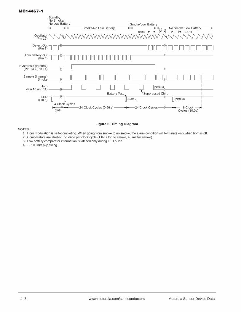
4–8 Motorola Sensor Device Datawww.motorola.com/semiconductors
Figure 6. Timing Diagram
Hysteresis (Internal)(Pin 13 ) (Pin 14)
Detect Out(Pin 1)
Low Battery Out(Pin 4)
Sample (Internal)Smoke
Horn(Pin 10 and 11)
LED(Pin 5)
Oscillator(Pin 12)
Standby
Smoke/No Low BatterySmoke/Low Battery
No Smoke/No Low Battery
No Smoke/Low Battery40 ms
10 ms1.67 s
24 Clock Cycles (0.96 s)24 Clock Cycles
(40S)24 Clock Cycles 6 Clock
Suppressed ChirpBattery Test
(Note 3) (Note 3)
(Note 1)
Cycles (10.0s)
NOTES:1. Horn modulation is self–completing. When going from smoke to no smoke, the alarm condition will terminate only when horn is off.2. Comparators are strobed on once per clock cycle (1.67 s for no smoke, 40 ms for smoke).3. Low battery comparator information is latched only during LED pulse.4. 100 mV p–p swing.

4–9Motorola Sensor Device Data www.motorola.com/semiconductors
Low–Power CMOS
The MC14468, when used with an ionization chamber and a small number ofexternal components, will detect smoke. When smoke is sensed, an alarm is soundedvia an external piezoelectric transducer and internal drivers. This circuit is designed tooperate in smoke detector systems that comply with UL217 and UL268 specifications.
• Ionization Type with On–Chip FET Input Comparator
• Piezoelectric Horn Driver
• Guard Outputs on Both Sides of Detect Input
• Input–Production Diodes on the Detect Input
• Low–Battery Trip Point, Internally Set, can be Altered Via External Resistor
• Detect Threshold, Internally Set, can be Altered Via External Resistor
• Pulse Testing for Low Battery Uses LED for Battery Loading
• Comparator Output for Detect
• Internal Reverse Battery Protection
• Strobe Output for External Trim Resistors
• I/O Pin Allows Up to 40 Units to be Connected for Common Signaling
• Power–On Reset Prevents False Alarms on Battery Change
MAXIMUM RATINGS* (Voltages referenced to VSS)
Rating Symbol Value Unit
DC Supply Voltage VDD 0.5 to + 15 V
Input Voltage, All Inputs Except Pin 8 Vin 0.25 to VDD + 0.25 V
DC Current Drain per Input Pin, Except Pin 15 = 1 mA I 10 mA
DC Current Drain per Output Pin I 30 mA
Operating Temperature Range TA 10 to + 60 °C
Storage Temperature Range Tstg 55 to + 125 °C
Reverse Battery Time tRB 5.0 s
* Maximum Ratings are those values beyond which damage to the device may occur.
This device contains circuitry to protect the inputs against damage due to high static voltages or electric fields; however, it is advised that normalprecautions be taken to avoid application of any voltage higher than maximum rated voltages to this high impedance circuit. For proper operationit is recommended that Vin and Vout be constrained to the range VSS (Vin or Vout) VDD.
SEMICONDUCTOR TECHNICAL DATA
P SUFFIXPLASTIC DIPCASE 648–08
PIN ASSIGNMENT(16 PIN DIP)
16
15
14
13
12
11
10
9
1
2
3
4
5
6
7
8
DetectComp. Out
I/O
Low V Set
StrobeOut
LED
VDD
TimingResistor
Feedback
Guard Hi–Z
Detect Input
Guard Lo–Z
Sensitivity Set
Osc Capacitor
Silver
Brass
VSS
ORDERING INFORMATION
MC14468P PLASTIC DIP
1
16
REV 3

4–10 Motorola Sensor Device Datawww.motorola.com/semiconductors
RECOMMENDED OPERATING CONDITIONS (Voltages referenced to VSS)
Parameter Symbol Value Unit
Supply Voltage VDD 9.0 V
Timing Capacitor — 0.1 µF
Timing Resistor — 8.2 MΩ
Battery Load (Resistor or LED) — 10 mA
ELECTRICAL CHARACTERISTICS (TA = 25°C)
Characteristic SymbolVDDVdc Min Typ# Max Unit
Operating Voltage VDD — 6.0 — 12 V
Output VoltagePiezoelectric Horn Drivers (IOH = 16 mA)Comparators (IOH = 30 µA)Piezoelectric Horn Drivers (IOL = +16 mA)Comparators (IOL = +30 µA)
VOH
VOL
7.29.07.29.0
6.38.5——
—8.8—0.1
——0.90.5
V
V
Output Voltage — LED Driver, IOL = 10 mA VOL 7.2 — — 3.0 V
Output Impedance, Active GuardPin 14Pin 16
Lo–ZHi–Z
9.09.0
——
——
101000
kΩ
Operating Current (Rbias = 8.2 MΩ) IDD 9.012.0
——
5.0—
9.012.0
µA
Input Current — Detect (40% R.H.) Iin 9.0 — — 1.0 pA
Input Current, Pin 8 Iin 9.0 — — 0.1 µA
Input Current @ 50°C, Pin 15 Iin — — — 6.0 pA
Internal Set VoltageLow BatterySensitivity
VlowVset
9.0—
7.247
—50
7.853
V%VDD
Hysteresis vhys 9.0 75 100 150 mV
Offset Voltage (measured at Vin = VDD/2)Active GuardDetect Comparator
VOS9.09.0
——
——
10050
mV
Input Voltage Range, Pin 8 Vin — VSS 10 — VDD + 10 V
Input Capacitance Cin — — 5.0 — pF
Common Mode Voltage Range, Pin 15 Vcm — 0.6 — VDD 2 V
I/O Current, Pin 2Input, VIH = VDD 2Output, VOH = VDD 2
IIHIOH
——
254.0
——
10016
µAmA
# Data labelled “Typ’’ is not to be used for design purposes but is intended as an indication of the IC’s potential performance.
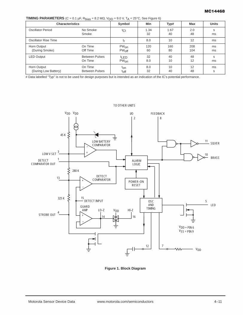
4–11Motorola Sensor Device Data www.motorola.com/semiconductors
TIMING PARAMETERS (C = 0.1 µF, Rbias = 8.2 MΩ, VDD = 9.0 V, TA = 25°C, See Figure 6)
Characteristics Symbol Min Typ# Max Units
Oscillator Period No SmokeSmoke
tCI 1.3432
1.6740
2.048
sms
Oscillator Rise Time tr 8.0 10 12 ms
Horn Output On Time(During Smoke) Off Time
PWonPWoff
12060
16080
208104
msms
LED Output Between PulsesOn Time
tLEDPWon
328.0
4010
4812
sms
Horn Output On Time(During Low Battery) Between Pulses
tontoff
8.032
1040
1248
mss
# Data labelled “Typ’’ is not to be used for design purposes but is intended as an indication of the IC’s potential performance.
Figure 1. Block Diagram
+
–
VDD
LOW BATTERYCOMPARATOR
POWER–ONRESET
+
–
VDD
45 K
3
280 K
712
13
325 K
+
–
15DETECT INPUT
14
LO–Z
16
HI–Z
VDD
VDD
8
11
10
5
LOW V SET
1DETECTCOMPARATOR OUT
ALARMLOGIC
DETECTCOMPARATOR
I/O2
OSCAND
TIMING
SILVER
BRASS
GUARDAMP
STROBE OUT4
LED
FEEDBACK
TO OTHER UNITS
VDD = PIN 6VSS = PIN 9
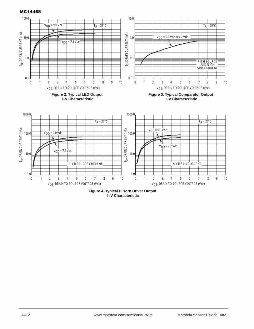
4–12 Motorola Sensor Device Datawww.motorola.com/semiconductors
Figure 2. Typical LED Output I–V Characteristic
Figure 3. Typical Comparator Output I–V Characteristic
Figure 4. Typical P Horn Driver Output I–V Characteristic
0 1 2 3 4 5 6 7 8 9 100.1
1.0
10.0
100.0
TA = 25°C
VDS, DRAIN TO SOURCE VOLTAGE (Vdc)
VDD = 7.2 Vdc
VDD = 9.0 Vdc
0 1 2 3 4 5 6 7 8 9 101.0
10.0
100.0
1000.0
DI ,
DR
AIN
CU
RR
ENT
(mA)
TA = 25°C
VDS, DRAIN TO SOURCE VOLTAGE (Vdc)
P–CH SOURCE CURRENT
VDD = 7.2 Vdc
VDD = 9.0 Vdc
0 1 2 3 4 5 6 7 8 9 101.0
10.0
100.0
1000.0
DI ,
DR
AIN
CU
RR
ENT
(mA)TA = 25°C
VDS, DRAIN TO SOURCE VOLTAGE (Vdc)
N–CH SINK CURRENT
VDD = 7.2 Vdc
VDD = 9.0 Vdc
0 1 2 3 4 5 6 7 8 9 100.01
0.1
1.0
10.0
DI ,
DR
AIN
CU
RR
ENT
(mA)
TA = 25°C
VDS, DRAIN TO SOURCE VOLTAGE (Vdc)
P–CH SOURCEAND N–CH
SINK CURRENT
VDD = 9.0 Vdc or 7.2 Vdc
DI ,
DR
AIN
CU
RR
ENT
(mA)

4–13Motorola Sensor Device Data www.motorola.com/semiconductors
DEVICE OPERATION
TIMINGThe internal oscillator of the MC14468 operates with a
period of 1.67 seconds during no–smoke conditions. Each1.67 seconds, internal power is applied to the entire IC and acheck is made for smoke, except during LED pulse, Low Bat-tery Alarm Chirp, or Horn Modulation (in smoke). Every 24clock cycles a check is made for low battery by comparingVDD to an internal zener voltage. Since very small currentsare used in the oscillator, the oscillator capacitor should be ofa low leakage type.
DETECT CIRCUITRYIf smoke is detected, the oscillator period becomes 40 ms
and the piezoelectric horn oscillator circuit is enabled. Thehorn output is modulated 160 ms on, 80 ms off. During the offtime, smoke is again checked and will inhibit further horn out-put if no smoke is sensed. During local smoke conditions thelow battery alarm is inhibited, but the LED pulses at a 1.0 Hzrate. In remote smoke, the LED is inhibited as well.
An active guard is provided on both pins adjacent to thedetect input. The voltage at these pins will be within 100 mVof the input signal. This will keep surface leakage currents toa minimum and provide a method of measuring the input volt-age without loading the ionization chamber. The active guardop amp is not power strobed and thus gives constant protec-tion from surface leakage currents. Pin 15 (the Detect input)has internal diode protection against static damage.
INTERCONNECTThe I/O (Pin 2), in combination with VSS, is used to inter-
connect up to 40 remote units for common signaling. A LocalSmoke condition activates a current limited output driver,thereby signaling Remote Smoke to interconnected units. Asmall current sink improves noise immunity during non–smoke conditions. Remote units at lower voltages do not
draw excessive current from a sending unit at a higher volt-age. The I/O is disabled for three oscillator cycles after powerup, to eliminate false alarming of remote units when the bat-tery is changed.
SENSITIVITY/LOW BATTERY THRESHOLDSBoth the sensitivity threshold and the low battery voltage
levels are set internally by a common voltage divider (pleasesee Figure 1) connected between VDD and VSS. These volt-ages can be altered by external resistors connected frompins 3 or 13 to either VDD or VSS. There will be a slight inter-action here due to the common voltage divider network. Thesensitivity threshold can also be set by adjusting the smokechamber ionization source.
TEST MODESince the internal op amps and comparators are power
strobed, adjustments for sensitivity or low battery level couldbe difficult and/or time–consuming. By forcing Pin 12 to VSS,the power strobing is bypassed and the output, Pin 1,constantly shows smoke/no smoke. Pin 1 = VDD for smoke.In this mode and during the 10 ms power strobe, chip currentrises to approximately 50 µA.
LED PULSEThe 9–volt battery level is checked every 40 seconds dur-
ing the LED pulse. The battery is loaded via a 10 mA pulsefor 10 ms. If the LED is not used, it should be replaced withan equivalent resistor such that the battery loading remainsat 10 mA.
HYSTERESISWhen smoke is detected, the resistor/divider network that
sets sensitivity is altered to increase sensitivity. This yieldsapproximately 100 mV of hysteresis and reduces falsetriggering.
Figure 5. Typical Application as Ionization Smoke Detector
MC144681 16
2
3
4
5
6
7
8
15
14
13
12
11
10
9
330 Ω
8.2 MΩ+
9 V0.1 µF
1.5 MΩ*0.001 µF 220 kΩ*
0.1 µF
1 M 1 M
TEST
*NOTE: Component values may changedepending on type of piezoelectric horn used.
TOOTHERUNITS

4–14 Motorola Sensor Device Datawww.motorola.com/semiconductors
Figure 6. Timing Diagram
Hysteresis (Internal)(Pin 13 ) (Pin 14)
Detect Out(Pin 1)
Low Battery(Internal)
Sample (Internal)Smoke
Horn(Pin 10 and 11)
LED(Pin 5)
Oscillator(Pin 12)
Standby
Smoke/No Low BatterySmoke/Low Battery
No Smoke/No Low Battery
No Smoke/Low Battery40 ms
10 ms1.67 s
24 Clock Cycles (0.96 s)24 Clock Cycles
(40S)24 Clock Cycles 6 Clock
Suppressed ChirpBattery Test
(Note 3) (Note 3)
(Note 1)
Cycles (10.0 s)Strobe Out
(Pin 14)
I/O (Pin 2)Output (Local)
I/O (Pin 2)Input (Remote)
LED
Note: Horn Modulation Not Self–Completing
Low = DisableHigh = Enable
(Suppressed LED for Remote Only)
NOTES:1. Horn modulation is self–completing. When going from smoke to no smoke, the alarm condition will terminate only when horn is off.2. Comparators are strobed on once per clock cycle (1.67 s for no smoke, 40 ms for smoke).3. Low battery comparator information is latched only during LED pulse.4. 100 mV p–p swing.

4–15Motorola Sensor Device Data www.motorola.com/semiconductors
CMOS
The MC14578 is an analog building block consisting of a very–high inputimpedance comparator. The voltage follower allows monitoring the noninvertinginput of the comparator without loading.
Four enhancement–mode MOSFETs are also included on chip. These FETs canbe externally configured as open–drain or totem–pole outputs. The drains haveon–chip static–protecting diodes. Therefore, the output voltage must be main-tained between VSS and VDD.
The chip requires one external component. A 3.9 MΩ 10% resistor must beconnected from the Rbias pin to VDD. This circuit is designed to operate in smokedetector systems that comply with UL217 and UL268 specifications.
• Applications:Pulse Shapers Line–Powered Smoke DetectorsThreshold Detectors Liquid/Moisture SensorsLow–Battery Detectors CO Detector and Micro Interface
• Operating Voltage Range: 3.5 to 14 V
• Operating Temperature Range: 30° to 70°C• Input Current (IN + Pin): 1 pA @ 25°C (DIP Only)
• Quiescent Current: 10 µA @ 25°C• Electrostatic Discharge (ESD) Protection Circuitry on All Pins
SEMICONDUCTOR TECHNICAL DATA
P SUFFIXPLASTIC DIPCASE 648–08
PIN ASSIGNMENT
16
15
14
13
12
11
10
9
1
2
3
4
5
6
7
8
COMP OUT
IN A
IN B
VDD
OUT B
IN C
OUT C1
NC
IN +
NC
BUFF OUT
IN—
Rbias
VSS
OUT C2
ORDERING INFORMATION
MC14578P PLASTIC DIP
116
OUT A
LOGIC DETAIL
2+
–COMP
BIASCKT
+
–BUFF
COMP OUT
13BUFF OUT
15IN+
12IN
11Rbias
IN A
IN B
3
4
5
6
OUT A
OUT B
9
8
OUT C2
OUT C1
7IN C
PIN 1 = VDDPIN 10 = VSSPINS 14, 16 = NO CONNECTION
REV 1

4–16 Motorola Sensor Device Datawww.motorola.com/semiconductors
MAXIMUM RATINGS* (Voltages Referenced to VSS)
Symbol Parameter Value Unit
VDD DC Supply Voltage 0.5 to +14 V
Vin DC Input Voltage 0.5 to VDD +0.5 V
Vout DC Output Voltage 0.5 to VDD +0.5 V
Iin DC Input Current, Except IN + 10 mA
Iin DC Input Current, IN + 1.0 mA
Iout DC Output Current, per Pin 25 mA
IDD DC Supply Current, VDD and VSS Pins 50 mA
PD Power Dissipation, per Package 500 mW
Tstg Storage Temperature 65 to +150 °C
TL Lead Temperature (10–Second Soldering) 260 °C
*Maximum Ratings are those values beyond which damage to the device may occur.
This device contains protection circuitry to guard against damage due to high static voltages or electric fields. However, precautions mustbe taken to avoid applications of any voltage higher than maximum rated voltages to this high–impedance circuit. For proper operation, Vin andVout should be constrained to the range VSS ≤ (Vin or Vout) ≤ VDD.
Unused inputs must always be tied to an appropriate logic voltage level (e.g., either VSS or VDD). Unused outputs must be left open.

4–17Motorola Sensor Device Data www.motorola.com/semiconductors
ELECTRICAL CHARACTERISTICS (Voltages Referenced to VSS, Rbias = 3.9 MΩ to VDD, TA = –30° to 70°C Unless Otherwise Indicated)
Symbol Parameter Test ConditionVDD
VGuaranteed
Limit Unit
VDD Power Supply Voltage Range — 3.5 to 14.0 V
VIL Maximum Low–Level Input Voltage, MOSFETsWired as Inverters; i.e., IN A tied to IN B, OUTA to OUT B, OUT C1 to OUT C2.
Vout = 9.0 V, |Iout| 1 µA 10.0 2.0 V
VIH Minimum High–Level Input Voltage, MOSFETsWired as Inverters; i.e., IN A tied to IN B, OUTA to OUT B, OUT C1 to OUT C2.
Vout = 1.0 V, |Iout| 1 µA 10.0 8.0 V
VIO Comparator Input Offset Voltage TA = 25°C, Over Common ModeRange
10.0 50 mV
TA = 0° to 50°C, Over CommonMode Range
3.5 to14.0
75
VCM Comparator Common Mode Voltage Range 3.5 to14.0
0.7 toVDD 1.5
V
VOL Maximum Low–Level Comparator Output Voltage IN +: Vin = VSS, IN : Vin = VDD, Iout = 30 µA
10.0 0.5 V
VOH Minimum High–Level Comparator Output Voltage IN +: Vin = VDD, IN : Vin = VSS, Iout = 30 µA
10.0 9.5 V
VOO Buffer Amp Output Offset Voltage Rload = 10 MΩ to VDD or VSS, OverCommon Mode Range
— 100 mV
VOL Maximum Low–Level Output Voltage, MOSFETsWired as Inverters; i e IN A tied to IN B OUT
OUT C1, OUT C2: Iout = 1.1 mA 10.0 0.5 VWired as Inverters i.e., IN A tied to IN B, OUTA to OUT B, OUT C1 to OUT C2. OUT A, OUT B: Iout = 270 µA 10.0 0.5 V
VOH Minimum High–Level Output Voltage, MOSFETsWired as Inverters; i e IN A tied to IN B OUT
OUT C1, OUT C2: Iout = 1.1 mA 10.0 9.5 VWired as Inverters i.e., IN A tied to IN B, OUTA to OUT B, OUT C1 to OUT C2. OUT A, OUT B: Iout = 270 µA 10.0 9.5 V
Iin Maximum Input Leakage IN + (DIP Only)Current
TA = 25°C, 40% R.H.,Vin = VSS or VDD
10.0 1.0 pA
IN + (DIP Only) TA = 50°C,Vin = VSS or VDD
10.0 6.0
IN + (SOG), IN A, IN B, IN C, IN Vin = VSS or VDD 10.0 40 nA
IOZ Maximum Off–State MOSFET Leakage Current IN A, IN C: Vin = VDD,OUT A, OUT C2: Vout = VSSor VDD
10.0 100 nA
IN B, IN C: Vin = VSS,OUT B, OUT C1: Vout = VSSor VDD
10.0 100
IDD Maximum Quiescent Current TA = 25°CIN A, IN B, IN C: Vin = VSS or VDD,|VIN + VIN| = 100 mV,
Iout = 0 µA
10.0 10 µA
Cin Maximum Input Capacitance IN +Other Inputs
f = 1 kHz ——
5.015
pF

4–18 Motorola Sensor Device Datawww.motorola.com/semiconductors
16
15
14
13
12
11
10
9
1
2
3
4
5
6
7
8
NC
IN +
NC
BUFF OUT
IN
Rbias
VSS
OUT C2
OUT A
OUT B
IN C
OUT C1
IN B
IN A
VDD
COMP OUT
R2
R1MC14578
R4
3.9 M
NOTE: IN + and IN have very high input impedance. Interconnect to these pins should be as short as possible.
Figure 1. Low–Battery Detector
V+
D1
R3
V+
V+
V+
R56.8 k
D2
LOW–BATTERYINDICATOR
OUTPUTHIGH = BATTERY LOWLOW = BATTERY OK
APPLICATIONS INFORMATION
EXAMPLE VALUES
Near the switchpoint, the comparator output in the circuitof Figure 1 may chatter or oscillate. This oscillation appearson the signal labelled OUTPUT. In some cases, the oscilla-tion in the transition region will not cause problems. Forexample, an MPU reading OUTPUT could sample the signaltwo or three times to ensure a solid level is attained. But, in alow battery detector, this probably is not necessary.
To eliminate comparator chatter, hysteresis can be addedas shown in Figure 2. The circuit of Figure 2 requires slightlymore operating current than the Figure 1 arrangement.
R1 R2 R3 Nominal Trip Point
470 kΩ 1.3 MΩ 20 kΩ 4.08 V
820 kΩ 1.2 MΩ 39 kΩ 5.05 V
1.2 MΩ 1.2 MΩ 62 kΩ 6.00 V
Figure 2. Adding Hysteresis
+–
R7
2
15
12
R6

4–19Motorola Sensor Device Data www.motorola.com/semiconductors
Low–Power CMOS with Horn Driver
The MC14600 Alarm IC is designed to simplify the process of interfacing analarm level voltage condition to a piezoelectric horn and/or LED. With an extremelylow average current requirement and an integrated low battery detect feature, thepart is ideally suited to battery operated applications. The MC14600 is easilyconfigured with a minimum number of external components to serve a wide rangeof applications and circuit configurations. Typical applications include intrusionalarms, moisture or water ingress alarms, and personal safety devices.
• High Impedance, FET Input Comparator
• Comparator Outputs for Low Battery and Alarm Detect
• Alarm Detect Threshold Easily Established with 2 Resistor
• Integrated Oscillator and Piezoelectric Horn Driver
• Low Battery Trip Point Set Internally (Altered Externally)
• Horn “Chirp’’ During Low Battery Condition
• Pulsed LED Drive Output
• Reverse Battery Protection
• Input Protection Diodes on the Detect Input
• Average Supply Current: 9 µA
MAXIMUM RATINGS* (Voltages referenced to VSS)
Rating Symbol Value Unit
DC Supply Voltage VDD 0.5 to + 15 V
Input Voltage, All Inputs Except Pin 8 Vin 0.25 to VDD + 0.25 V
DC Current Drain per Input Pin,Except Pin 15 = 1 mA
I 10 mA
DC Current Drain per Output Pin I 30 mA
Operating Temperature Range TA 10 to + 60°C °C
Storage Temperature Range Tstg 55 to + 125 °C
Reverse Battery Time tRB 5.0 s
* Maximum Ratings are those values beyond which damage to the device may occur.
This device contains circuitry to protect the inputs against damage due to high static voltagesor electric fields; however, it is advised that normal precautions be taken to avoid applicationof any voltage higher than maximum rated voltages to this high impedance circuit. For properoperation it is recommended that Vin and Vout be constrained to the range VSS (Vin or Vout) VDD.
SEMICONDUCTOR TECHNICAL DATA
P SUFFIXPLASTIC DIPCASE 648–08
PIN ASSIGNMENT(16 PIN DIP)
16
15
14
13
12
11
10
9
1
2
3
4
5
6
7
8
DetectComp. Out
N/C
Low V Set
Low VComp. Out
LED
VDD
TimingResistor
HornFeedback
Guard
AlarmDetect Input
N/C
AlarmThreshold
Osc Capacitor
Horn Out 2
Horn Out 1
VSS
ORDERING INFORMATION
1
16
MC14600P PLASTIC DIP
MC14600DW SOIC
MC14600DWR2 SOIC TAPE & REEL
DW SUFFIXSOIC PACKAGECASE 751G–03
1
16
REV 3

4–20 Motorola Sensor Device Datawww.motorola.com/semiconductors
RECOMMENDED OPERATING CONDITIONS (Voltages referenced to VSS)
Parameter Symbol Value Unit
Supply Voltage VDD 9.0 V
LED (Pin 5) Load — 10 mA
ELECTRICAL CHARACTERISTICS (Voltages referenced to VSS, TA = 25°C)
Characteristic Pin # SymbolVDDVdc Min Typ Max Unit
Operating Voltage 6 VDD — 6.0 — 12 V
Output VoltagePiezoelectric Horn Drivers (IOH = +16 mA)Comparators (IOH = +30 µA)Piezoelectric Horn Drivers (IOL = 16 mA)Comparators (IOL = 30 µA)
(IOL = 200 µA)
10,114
10,1141
VOH
VOL
7.49.07.49.0—
6.58.5———
—8.8—0.1—
——0.90.50.5
V
V
Output Voltage — LED Driver, IOL = 10 mA 5 VOL 7.2 — — 2.0 V
Output Impedance, Active Guard 16 Hi–Z 9.0 — — 1000 kΩ
Standby Current (Rbias = 8.2 MΩ) — IDD 9.012.0
——
5.0—
9.012.0
µA
Input Leakage Current 1813
—Iin—
9.09.09.0
———
———
300.130
nAµAnA
Detect Comp. Out V = 3 VV = 9 V
1 ——
——
2.50—
——
—8.00
mAmA
Low Battery Threshold Voltage (Pin 3 open) 6 Vlow 9.0 7.2 — 7.8 V
Offset Voltage (measured at Vin = VDD/2)Active GuardDetect Comparator
1613,15
VOS9.09.0
——
——
10050
mV
Input Voltage Range 8 Vin — VSS –10 — VDD + 10 V
Input Capacitance (to VSS @ 1 khz) 15 Cin — — 5.0 — pF
Common Mode Voltage Range 13,15 Vcm — 1.5 — VDD –2 V
Breakdown Voltage
Human Body Models per MIL–STD–883 Method 3015
All pinsexcept 15
15
—
—
—
—
500
400
—
—
—
—
V
# Data labelled “Typ’’ is not to be used for design purposes but is intended as an indication of the IC’s potential performance.

4–21Motorola Sensor Device Data www.motorola.com/semiconductors
TIMING PARAMETERS (Cosc = 0.1 µF, Rbias = 8.2 MΩ, VDD = 9.0 V, TA = 25°C, See Figure 2)
Characteristics Pin # Symbol Min Max Units
Oscillator Period (1 Clock Cycle = 1 Oscillator Period) No AlarmAlarm
12 tCI—
1.2530
2.2552
sms
Oscillator Pulse Width (No Alarm and Alarm Condition) 3,4,5,13 tr 7.0 13 ms
LED Output Period No AlarmAlarm
5 tLED—
30.71
521.25
sms
Alarm Horn Output Hi TimeLow Time
10,11 tontoff
12060
208104
msms
Low Battery Horn Output Hi TimeBetween Pulses
10,11 tontoff
7.030
1352
mss
Figure 1. Block Diagram
11
10
8HORN FEEDBACK
HORNOUT 2
HORNOUT 1
ALARMLOGIC
OSCAND
TIMING
5LED
VDD = PIN 6VSS = PIN 9
7VDD
+
–
LOW BATTERYCOMPARATOR
VDDLOW V COMP.
OUT4
VDD
3LOW V SET
1DETECT
COMPARATOR OUT
+
–13
DETECTCOMPARATORALARM
THRESHOLD
15ALARM DETECTINPUT
+
–
VDD HI–Z
16
GUARDAMP
12Cosc Rbias

4–22 Motorola Sensor Device Datawww.motorola.com/semiconductors
DEVICE OPERATION
TIMINGThe internal oscillator of the MC14600 operates with a
period of 1.65 seconds during no–alarm conditions. Each1.65 seconds, internal power is applied to the entire IC and acheck is made for an alarm input level except during LEDpulse, Low Battery Alarm Chirp, or Horn Modulation (inalarm). Every 24 clock cycles a check is made for low batteryby comparing VDD to an internal zener voltage. Since verysmall currents are used in the oscillator, the oscillator capaci-tor should be of a low leakage type.
DETECT CIRCUITRYIf an alarm condition is detected, the oscillator period
becomes 41.67 ms and the piezoelectric horn oscillator cir-cuit is enabled. The horn output is modulated 167 ms on,83 ms off. During the off time, alarm detect input (Pin 15) isagain checked and will inhibit further horn output if no alarmcondition is sensed. During alarm conditions the low batterychirp is inhibited, and the LED pulses at a 1.0 Hz rate.
An active guard is provided on a pin adjacent to the detectinput (Pin 16). The voltage at this pin will be within 100 mV ofthe input signal. Pin 16 will allow monitoring of the input sig-nal at pin 15 through a buffer. The active guard op amp is not
power strobed and thus gives constant protection from sur-face leakage currents. Pin 15 (the Detect input) has internaldiode protection against static damage.
LOW BATTERY THRESHOLDThe low battery voltage level is set internally by a voltage
divider connected between VDD and VSS. This voltage canbe altered by external resistors connected from pin 3 toeither VDD or VSS. A resistor to VDD will decrease the thresh-old while a resistor to GND will increase it.
ALARM THRESHOLD (SENSITIVITY)The alarm condition voltage level is set externally through
Pin 13. A voltage divider can be used to set the alarm trippoint. Pin 13 is connected internally to the negative input ofthe detect comparator.
LED PULSEThe 9–volt battery level is checked every 40 seconds dur-
ing the LED pulse. The battery is loaded via a 10 mA pulsefor 10 ms. If the LED is not used, it should be replaced withan equivalent resistor so that the battery loading remains at10 mA.
Figure 2. Typical Application Components
MC146001 16
2
3
4
5
6
7
8
15
14
13
12
11
10
9
330 Ω
Rbias0.1 µF
1.5 MΩ*0.001 µF 220 kΩ*
COSC
*NOTE: Component values may change depending on type of piezoelectric horn used.
DETECTINPUT
R1 R2VDD
Rp
VDD
VDD

4–23Motorola Sensor Device Data www.motorola.com/semiconductors
Figure 3. MC14600 Timing Diagram
OSCPIN 12
ALARM – N– Y
LOW BATTCOMP (PIN 4)
DETECT OUT(PIN 1)
LED – OFF– ON
2 3 4 5 6 7 98
NO ALARM, LOW BATTERY
1
NO ALARMNO LOW BAT
LOW BATTERY CHIRP
OSCPIN 12
ALARM – N– Y
NO ALARM
23 24 1 6 12 18 24
ALARM
LATCH ALARM CONDITION
HORN – ON– OFF
LED – OFF– ON
(NOTE 1)
24 CLOCKS 24 CLOCKS
HORN(PINS 10 AND 11)
LOW BATTCOMP
DETECT OUT(PIN 1)
NOTES:1. Horn modulation is self–completing. When going from Alarm to No Alarm, the alarm condition will terminate only when horn is off.2. Comparators are strobed once per cycle.3. Low battery comparator information is latched only during LED pulse.4. Current source required into Pin 1.5. Alarm Condition can initiate on any clock pulse except 1 and 7.

4–24 Motorola Sensor Device Datawww.motorola.com/semiconductors
The CMOS MC145010 is an advanced smoke detector componentcontaining sophisticated very–low–power analog and digital circuitry. The IC isused with an infrared photoelectric chamber. Detection is accomplished bysensing scattered light from minute smoke particles or other aerosols. Whendetection occurs, a pulsating alarm is sounded via on–chip push–pull driversand an external piezoelectric transducer.
The variable–gain photo amplifier allows direct interface to IR detectors(photodiodes). Two external capacitors, C1 and C2, C1 being the larger,determine the gain settings. Low gain is selected by the IC during most of thestandby state. Medium gain is selected during a local–smoke condition. High gainis used during pushbutton test. During standby, the special monitor circuit whichperiodically checks for degraded chamber sensitivity uses high gain, also.
The I/O pin, in combination with VSS, can be used to interconnect up to 40units for common signaling. An on–chip current sink provides noise immunitywhen the I/O is an input. A local–smoke condition activates the short–circuit–protected I/O driver, thereby signaling remote smoke to the interconnectedunits. Additionally, the I/O pin can be used to activate escape lights, enableauxiliary or remote alarms, and/or initiate auto–dialers.
While in standby, the low–supply detection circuitry conducts periodic checksusing a pulsed load current from the LED pin. The trip point is set using twoexternal resistors. The supply for the MC145010 can be a 9 V battery.
A visible LED flash accompanying a pulsating audible alarm indicates alocal–smoke condition. A pulsating audible alarm with no LED flash indicates aremote–smoke condition. A beep or chirp occurring virtually simultaneouslywith an LED flash indicates a low–supply condition. A beep occurring half–waybetween LED flashes indicates degraded chamber sensitivity. A low–supplycondition does not affect the smoke detection capability if VDD ≥ 6 V. Therefore,the low–supply condition and degraded chamber sensitivity can be furtherdistinguished by performing a pushbutton (chamber) test.
• Circuit is designed to operate in smoke detector systems that comply withUL217 and UL268 Specifications
• Operating Voltage Range: 6 to 12 V
• Operating Temperature Range: – 10 to 60°C• Average Supply Current: 12 µA
• Power–On Reset Places IC in Standby Mode (Non–Alarm State)
• Electrostatic Discharge (ESD) and Latch Up Protection Circuitry on All Pins
• Chip Complexity: 2000 FETs, 12 NPNs, 16 Resistors, and 10 Capacitors
• Ideal for battery powered applications.
SEMICONDUCTOR TECHNICAL DATA
P SUFFIXPLASTIC DIPCASE 648–08
PIN ASSIGNMENT
16
15
14
13
12
11
10
9
1
2
3
4
5
6
7
8
C1
C2
Detect
Strobe
VDD
IRED
I/O
Brass
Test
Low–SupplyTrip
VSS
R1
Osc
LED
Feedback
Silver
ORDERING INFORMATION
MC145010P PLASTIC DIP
MC145010DW SOIC PACKAGE
1
16
DW SUFFIXSOIC PACKAGECASE 751G–03
1
16
REV 4

4–25Motorola Sensor Device Data www.motorola.com/semiconductors
BLOCK DIAGRAM
+
–
+
–DETECT
OSC
R1
TEST
STROBE
LOW–SUPPLYTRIP
3
12
13
16
4
15
21C1 C2
OSC
AMPCOMP
COMP
ALARMLOGIC
HORN MODULATORAND DRIVER
VDD – 5 VREF
TIMINGLOGIC
VDD – 3.5 VREF
ZER
O
GAI
N
LOW
SU
PPLY
SMOKE
GATE
ON/OFF
GATEON/OFF
89
106
11
7
PIN 5 = VDDPIN 14 = VSS
LED
IREDFEEDBACK
SILVERBRASS
I/O
MAXIMUM RATINGS* (Voltages Referenced to VSS)
Symbol Parameter Value Unit
VDD DC Supply Voltage 0.5 to +12 V
Vin DC Input Voltage C1, C2, DetectOsc, Low–Supply Trip
I/OFeedback
Test
0.25 to VDD +0.250.25 to VDD +0.250.25 to VDD +1015 to +25
1.0 to VDD +0.25
V
Iin DC Input Current, per Pin 10 mA
Iout DC Output Current, per Pin 25 mA
IDD DC Supply Current, VDD and VSS Pins +25 / 150 mA
PD Power Dissipation in Still Air, 5 SecondsContinuous
1200**350***
mW
Tstg Storage Temperature 55 to +125 °C
TL Lead Temperature, 1 mm from Case for 10 Seconds 260 °C
* Maximum Ratings are those values beyond which damage to the device may occur. Functional operation should be restricted to the limits inthe Electrical Characteristics tables.
** Derating: – 12 mW/°C from 25° to 60°C.*** Derating: – 3.5 mW/°C from 25° to 60°C.
This device contains protection circuitry to guard against damage due to high static voltages or electric fields. However, precautions mustbe taken to avoid applications of any voltage higher than maximum rated voltages to this high–impedance circuit. For proper operation, Vin andVout should be constrained to the range VSS ≤ (Vin or Vout) ≤ VDD except for the I/O, which can exceed VDD, and the Test input, which can gobelow VSS.
Unused inputs must always be tied to an appropriate logic voltage level (e.g., either VSS or VDD). Unused outputs and/or an unused I/O mustbe left open.

4–26 Motorola Sensor Device Datawww.motorola.com/semiconductors
ELECTRICAL CHARACTERISTICS (TA = – 10 to 60°C Unless Otherwise Indicated, Voltages Referenced to VSS)
Symbol Parameter Test ConditionVDD
V Min Max Unit
VDD Power Supply Voltage Range — 6.0 12 V
VTH Supply Threshold Voltage, Low–SupplyAlarm
Low–Supply Trip: Vin = VDD/3 — 6.5 7.8 V
IDD Average Operating Supply Current(per Package)
Standby Configured per Figure 5
12.0 — 12 µA
iDD Peak Supply Current (per Package) During Strobe On, IRED OffConfigured per Figure 5
12.0 — 2.0 mA
During Strobe On, IRED OnConfigured per Figure 5
12.0 — 3.0
VIL Low–Level Input Voltage I/OFeedback
Test
9.09.09.0
———
1.52.77.0
V
VIH High–Level Input Voltage I/OFeedback
Test
9.09.09.0
3.26.38.5
———
V
Iin Input Current OSC, DetectLow–Supply Trip
Feedback
Vin = VSS or VDDVin = VSS or VDDVin = VSS or VDD
12.012.012.0
———
± 100± 100± 100
nA
IIL Low–Level Input Current Test Vin = VSS 12.0 — – 1 µA
IIH Pull–Down Current TestI/O
Vin = VDDNo Local Smoke, Vin = VDDNo Local Smoke, Vin = 17 V
9.09.012.0
0.525—
10100140
µA
VOL Low–Level Output Voltage LEDSilver, Brass
Iout = 10 mAIout = 16 mA
6.56.5
——
0.61.0
V
VOH High–Level Output Voltage Silver, Brass Iout = – 16 mA 6.5 5.5 — V
Vout Output Voltage Strobe(For Line Regulation, See PinDescriptions)
Inactive, Iout = –1 µAActive, Iout = 100 µA to 500 µA
(Load Regulation)
—9.0
VDD – 0.1VDD – 4.4
—VDD – 5.6
V
IRED Inactive, Iout = 1 µAActive, Iout = 6 mA
(Load Regulation)
—9.0
—2.25*
0.13.75*
IOH High–Level Output Current I/O Local Smoke, Vout = 4.5 V 6.5 – 4 — mA
Local Smoke, Vout = VSS(Short Circuit Current)
12.0 — – 16
IOZ Off–State Output Leakage Current LED Vout = VSS or VDD 12.0 — ± 1 µA
VIC Common Mode C1, C2, DetectVoltage Range
Local Smoke, Pushbutton Test, orChamber Sensitivity Test
— VDD – 4 VDD – 2 V
Vref Smoke Comparator InternalReference Voltage
Local Smoke, Pushbutton Test, orChamber Sensitivity Test
— VDD – 3.08 VDD – 3.92 V
* TA = 25°C only.

4–27Motorola Sensor Device Data www.motorola.com/semiconductors
AC ELECTRICAL CHARACTERISTICS (Reference Timing Diagram Figures 3 and 4)(TA = 25°C, VDD = 9.0 V, Component Values from Figure 5: R1 = 100.0 KΩ, C3 = 1500.0 pF, R2 = 10.0 MΩ)
No. Symbol Parameter Test Condition Clocks Min Max Unit
1 1/fosc Oscillator Period* Free–Running SawtoothMeasured at Pin 12
1 9.5 11.5 ms
2 tLED LED Pulse Period No Local Smoke, and No Remote Smoke
4096 38.9 47.1 s
3 Remote Smoke, but No Local Smoke
— None
4 Local Smoke or Pushbutton Test 64 0.60 0.74
5 tw(LED),tw(stb)
LED Pulse Width and StrobePulse Width
1 9.5 11.5 ms
6 tIRED IRED Pulse Period Smoke Test 1024 9.67 11.83 s
7 Chamber Sensitivity Test,without Local Smoke
4096 38.9 47.1
8 Pushbutton Test 32 0.302 0.370
9 tw(IRED) IRED Pulse Width Tf* 94 116 µs
10 tr IRED Rise Time — — 30 µs
tf IRED Fall Time — — 200
11 tmod Silver and Brass ModulationPeriod
Local or Remote Smoke — 297 363 ms
11,12 ton/tmod Silver and Brass Duty Cycle Local or Remote Smoke — 73 77 %
13 tCH Silver and Brass Chirp PulsePeriod
Low Supply or DegradedChamber Sensitivity
4096 38.9 47.1 s
14 tw(CH) Silver and Brass Chirp PulseWidth
Low Supply or DegradedChamber Sensitivity
1 9.5 11.5 ms
15 tRR Rising Edge on I/O to SmokeAlarm Response Time
Remote Smoke,No Local Smoke
— — 800 ms
16 tstb Strobe Out Pulse Period Smoke Test 1024 9.67 11.83 s
17 Chamber Sensitivity Test,without Local Smoke
4096 38.9 47.1
18 Low Supply Test, without Local Smoke
4096 38.9 47.1
19 Pushbutton Test — 0.302 0.370
* Oscillator period T (= Tr + Tf) is determined by the external components R1, R2, and C3 where Tr = (0.6931) R2 * C3 and Tf = (0.6931) R1 * C3.
The other timing characteristics are some multiple of the oscillator timing as shown in the table.

4–28 Motorola Sensor Device Datawww.motorola.com/semiconductors
Figure 1. AC Characteristics versus Supply
PULSE WIDTH OF IRED
PERIOD OR PULSE WIDTHOF OTHER PARAMETERS
AC P
ARAM
ETER
(NO
RM
ALIZ
ED T
O 9
.0 V
VAL
UE)
VDD, POWER SUPPLY VOLTAGE (V)
1.02
0.98
0.96
1.00
1.04
6.0 7.0 8.0 9.0 10.0 11.0 12.0
TA = 25°C
Figure 2A. AC Characteristics versus Temperature
NOTE: Includes external component variations. See Figure 2B.
PULSE WIDTH OF IRED
PERIOD OR PULSE WIDTHOF OTHER PARAMETERS
AC P
ARAM
ETER
(NO
RM
ALIZ
ED T
O 2
5C
VAL
UE)
°
TA, AMBIENT TEMPERATURE (°C)
– 10 0 10 20 30 40 50 60
1.02
1.01
0.99
0.98
1.00
VDD = 9.0 V
Figure 2.
Figure 2B. RC Component Variation Over Temperature
NOTE: These components were used to generate Figure 2A.
10 MΩ CARBON COMPOSITION
100 kΩ METAL FILM
1500 pF DIPPED MICA
CO
MPO
NEN
T VA
LUE
(NO
RM
ALIZ
ED T
O25
C V
ALU
E)°
TA, AMBIENT TEMPERATURE (°C)
– 10 0 10 20 30 40 50 60
1.03
1.02
1.01
1.00
0.99
0.98

4–29M
otorola Sensor D
evice Data
ww
w.m
otorola.com/sem
iconductors
Figure 3. S
tandby Timing D
iagram
LOW SUPPLY TEST(INTERNAL)
SMOKE TEST(INTERNAL)
CHAMBER TEST(INTERNAL)
7
OSC(PIN 12)
1
LED(PIN 11)
SILVER, BRASS
(INTERNAL)ENABLE
213 13
POWER–ON RESETNO LOW SUPPLY
CHIRPS
IRED(PIN 6)
STROBE(PIN 4)
6 6
16 17
5 14
18
NOTES: Numbers refer to the AC Electrical Characteristics Table.Illustration is not to scale.
CHAMBER SENSITIVITY OKINDICATE
LOW SUPPLY
CHIRPSINDICATE
DEGRADEDCHAMBER
SENSITIVITY
9

4–30M
otorola Sensor D
evice Data
ww
w.m
otorola.com/sem
iconductors
Figure 4. S
moke Tim
ing Diagram
LOW SUPPLY TEST(INTERNAL)
IRED(PIN 6)
CHAMBER TEST(INTERNAL)
STROBE(PIN 4)
6
I/O(PIN 7)
SILVER, BRASS
(NOT PERFORMED)
(NOT PERFORMED)
1110
9
IRED10%
90%
5
8
19
LED(PIN 11)
5 43
(NO PULSES)
(AS INPUT) (AS OUTPUT)(AS OUTPUT)
ENABLE (INTERNAL)
1512
11
NOSMOKE
PUSHBUTTONNO SMOKELOCAL SMOKE(REMOTE SMOKE = DON’T CARE)
REMOTE SMOKE(NO LOCAL SMOKE)
4
NOTES: Numbers refer to the AC Electrical Characteristics Table.Illustration is not to scale.
TEST

4–31Motorola Sensor Device Data www.motorola.com/semiconductors
16
15
14
13
12
11
10
9
1
2
3
4
5
6
7
8
TEST
LOW–SUPPLYTRIP
VSS
R1
OSC
LED
FEEDBACK
SILVER
VDD
IRED
I/O
BRASS
STROBE
DETECT
C1
C2
HORN
X1TO OTHERMC145010(s),
ESCAPE LIGHT(S),AUXILIARY ALARM(S),
REMOTE ALARM(S),AND/OR AUTO–DIALER
IRCURRENT
R13*4.7 TO 22
Q1
2.2 MR5
D4VISIBLELED
R747 k
R6100 k
SW1+
+
MC145010
REVERSE POLARITYPROTECTION
CIRCUIT
PUSHBUTTONTEST
R210 M
0.01 µFC6
C31500 pF
R1100 k
R3
470
R4
100 k
9 VB1 D11 TO 22 µF
C4**
C10.047 µF
C2*4700 pF
R14560 Ω
R11 250 k
D2IR DETECTOR
R88.2 k
R9†
5 k
R104.7 k
D3IR EMITTER
R121 k
C5100 µF
Values for R4, R5, and C6 may differ depending on type of piezoelectric horn used.* C2 and R13 are used for coarse sensitivity adjustment. Typical values are shown.†R9 is for fine sensitivity adjustment (optional). If fixed resistors are used, R8 = 12 k, R10 is 5.6 k to 10 k, and R9 is eliminated.
When R9 is used, noise pickup is increased due to antenna effects. Shielding may be required.**C4 should be 22 µF if B1 is a carbon battery. C4 could be reduced to 1 µF when an alkaline battery is used.
Figure 5. Typical Battery–Powered Application
PIN DESCRIPTIONS
C1 (Pin 1)A capacitor connected to this pin as shown in Figure 5
determines the gain of the on–chip photo amplifier duringpushbutton test and chamber sensitivity test (high gain). Thecapacitor value is chosen such that the alarm is tripped frombackground reflections in the chamber during pushbuttontest.
Av ≈ 1 + (C1/10) where C1 is in pF. CAUTION: The valueof the closed–loop gain should not exceed 10,000.
C2 (Pin 2)A capacitor connected to this pin as shown in Figure 5
determines the gain of the on–chip photo amplifier exceptduring pushbutton or chamber sensitivity tests.
Av ≈ 1 + (C2/10) where C2 is in pF. This gain increasesabout 10% during the IRED pulse, after two consecutivelocal smoke detections.
Resistor R14 must be installed in series with C2. R14 ≈[1/(12√C2)] – 680 where R14 is in ohms and C2 is in farads.
DETECT (Pin 3)This input to the high–gain pulse amplifier is tied to the
cathode of an external photodiode. The photodiode shouldhave low capacitance and low dark leakage current. Thediode must be shunted by a load resistor and is operated atzero bias.
The Detect input must be ac/dc decoupled from all othersignals, VDD, and VSS. Lead length and/or foil traces to thispin must be minimized, also. See Figure 6.
STROBE (Pin 4)This output provides a strobed, regulated voltage refer-
enced to VDD. The temperature coefficient of this voltage is± 0.2%/°C maximum from – 10° to 60°C. The supply–voltagecoefficient (line regulation) is ± 0.2%/V maximum from 6 to12 V. Strobe is tied to external resistor string R8, R9, andR10.

4–32 Motorola Sensor Device Datawww.motorola.com/semiconductors
VDD (Pin 5)This pin is connected to the positive supply potential and
may range f rom +6 to +12 V wi th respect to VSS.CAUTION: In battery–powered applications, reverse–polarity protection must be provided externally.
IRED (Pin 6)This output provides pulsed base current for external NPN
transistor Q1 used as the infrared emitter driver. Q1 musthave β ≥ 100. At 10 mA, the temperature coefficient of theoutput voltage is typically + 0.5%/°C from – 10° to 60°C. Thesupply–voltage coefficient (line regulation) is ± 0.2%/V maxi-mum from 6 to 12 V. The IRED pulse width (active–high) isdetermined by external components R1 and C3. With a100 kΩ/1500 pF combination, the nominal width is 105 µs.
To minimize noise impact, IRED is not active when the vis-ible LED and horn outputs are active. IRED is active near theend of Strobe pulses for Smoke Tests, Chamber SensitivityTest, and Pushbutton Test.
I/O (Pin 7)This pin can be used to connect up to 40 units together in
a wired–OR configuration for common signaling. VSS is usedas the return. An on–chip current sink minimizes noise pickup during non–smoke conditions and eliminates the need foran external pull–down resistor to complete the wired–OR.Remote units at lower supply voltages do not draw excessivecurrent from a sending unit at a higher supply voltage.
I/O can also be used to activate escape lights, auxiliaryalarms, remote alarms, and/or auto–dialers.
As an input, this pin feeds a positive–edge–triggered flip–flop whose output is sampled nominally every 625 ms duringstandby (using the recommended component values). Alocal–smoke condition or the pushbutton–test mode forcesthis current–limited output to source current. All input signalsare ignored when I/O is sourcing current.
I/O is disabled by the on–chip power–on reset to elimi-nate nuisance signaling during battery changes or systempower–up.
If unused, I/O must be left unconnected.
BRASS (Pin 8)This half of the push–pull driver output is connected to the
metal support electrode of a piezoelectric audio transducerand to the horn–starting resistor. A continuous modulatedtone from the transducer is a smoke alarm indicating eitherlocal or remote smoke. A short beep or chirp is a troublealarm indicating a low supply or degraded chambersensitivity.
SILVER (Pin 9)This half of the push–pull driver output is connected to the
ceramic electrode of a piezoelectric transducer and to thehorn–starting capacitor.
FEEDBACK (Pin 10)This input is connected to both the feedback electrode of a
self–resonating piezoelectric transducer and the horn–start-ing resistor and capacitor through current–limiting resistorR4. If unused, this pin must be tied to VSS or VDD.
LED (Pin 11)This active–low open–drain output directly drives an exter-
nal visible LED at the pulse rates indicated below. The pulsewidth is equal to the OSC period.
The load for the low–supply test is applied by this output.This low–supply test is non–coincident with the smoke tests,chamber sensitivity test, pushbutton test, or any alarmsignals.
The LED also provides a visual indication of the detectorstatus as follows, assuming the component values shown inFigure 5:
Standby (includes low–supply and chamber sensitivitytests) — Pulses every 43 seconds (nominal)
Local Smoke — Pulses every 0.67 seconds (nominal)
Remote Smoke — No pulses
Pushbutton Test — Pulses every 0.67 seconds (nominal)
OSC (Pin 12)This pin is used in conjunction with external resistor R2
(10 MΩ) to VDD and external capacitor C3 (1500 pF) to VDDto form an oscillator with a nominal period of 10.5 ms.
R1 (Pin 13)This pin is used in conjunction with resistor R1 (100 kΩ) to
pin 12 and C3 (1500 pF, see pin 12 description) to determinethe IRED pulse width. With this RC combination, the nominalpulse width is 105 µs.
VSS (Pin 14)This pin is the negative supply potential and the return for
the I/O pin. Pin 14 is usually tied to ground.
LOW–SUPPLY TRIP (Pin 15)This pin is connected to an external voltage which deter-
mines the low–supply alarm threshold. The trip voltage isobtained through a resistor divider connected between theVDD and LED pins. The low–supply alarm threshold voltage(in volts) ≈ (5R7/R6) + 5 where R6 and R7 are in the sameunits.
TEST (Pin 16)This input has an on–chip pull–down device and is used to
manually invoke a test mode.The Pushbutton Test mode is initiated by a high level at pin
16 (usually depression of a S.P.S.T. normally–open pushbut-ton switch to VDD). After one oscillator cycle, IRED pulsesapproximately every 336 ms, regardless of the presence ofsmoke. Additionally, the amplifier gain is increased by auto-matic selection of C1. Therefore, the background reflectionsin the smoke chamber may be interpreted as smoke, gener-ating a simulated–smoke condition. After the second IREDpulse, a successful test activates the horn–driver and I/O cir-cuits. The active I/O allows remote signaling for system test-ing. When the Pushbutton Test switch is released, the Testinput returns to VSS due to the on–chip pull–down device.After one oscillator cycle, the amplifier gain returns to nor-mal, thereby removing the simulated–smoke condition. Aftertwo additional IRED pulses, less than a second, the IC exitsthe alarm mode and returns to standby timing.

4–33Motorola Sensor Device Data www.motorola.com/semiconductors
CALIBRATION
To facilitate checking the sensitivity and calibrating smokedetectors, the MC145010 can be placed in a calibrationmode. In this mode, certain device pins are controlled/recon-figured as shown in Table 1. To place the part in the calibra-tion mode, pin 16 (Test) must be pulled below the VSS pin
with 100 µA continuously drawn out of the pin for at least onecycle on the OSC pin. To exit this mode, the Test pin isfloated for at least one OSC cycle.
In the calibration mode, the IRED pulse happens at everyclock cycle and strobe is always on (active low). Also, LowBattery and supervisory tests are disabled in this mode.
Table 1. Configuration of Pins in the Calibration Mode
Description Pin Comment
I/O 7 Disabled as an output. Forcing this pin high places the photo amp output on pin 1 or 2, as determined byLow–Supply Trip. The amp’s output appears as pulses and is referenced to VDD.
Low–Supply Trip 15 If the I/O pin is high, pin 15 controls which gain capacitor is used. Low: normal gain, amp output on pin 1.High: supervisory gain, amp output on pin 2.
Feedback 10 Driving this input high enables hysteresis (10% gain increase) in the photo amp; pin 15 must be low.
OSC 12 Driving this input high brings the internal clock high. Driving the input low brings the internal clock low. Ifdesired, the RC network for the oscillator may be left intact; this allows the oscillator to run similar to thenormal mode of operation.
Silver 9 This pin becomes the smoke comparator output. When the OSC pin is toggling, positive pulses indicatethat smoke has been detected. A static low level indicates no smoke.
Brass 8 This pin becomes the smoke integrator output. That is, 2 consecutive smoke detections are required for“on” (static high level) and 2 consecutive no–detections for “off” (static low level).
NOTES: Illustration is bottom view of layout using a DIP. Top view for SOIC layout is mirror image.Optional potentiometer R9 is not included.Drawing is not to scale.Leads on D2, R11, R8, and R10 and their associated traces must be kept as short as possible.
This practice minimizes noise pick up. Pin 3 must be decoupled from all other traces.
Figure 6. Recommended PCB Layout
DO NOT RUN ANYADDITIONAL TRACES
IN THIS REGION
PIN 8
PIN 16
PIN 9
PIN 1
C1
R14
R11
D2
R8
MOUNTED INCHAMBER
C2
R10

4–34 Motorola Sensor Device Datawww.motorola.com/semiconductors
For Line–Powered Applications
The CMOS MC145011 is an advanced smoke detector component containingsophisticated very–low–power analog and digital circuitry. The IC is used with aninfrared photoelectric chamber. Detection is accomplished by sensing scatteredlight from minute smoke particles or other aerosols. When detection occurs, apulsating alarm is sounded via on–chip push–pull drivers and an externalpiezoelectric transducer.
The variable–gain photo amplifier allows direct interface to IR detectors(photo–diodes). Two external capacitors C1 and C2, C1 being the larger,determine the gain settings. Low gain is selected by the IC during most of thestandby state. Medium gain is selected during a local–smoke condition. High gainis used during pushbutton test. During standby, the special monitor circuit whichperiodically checks for degraded chamber sensitivity uses high gain, also.
The I/O pin, in combination with VSS, can be used to interconnect up to 40 unitsfor common signaling. An on–chip current sink provides noise immunity when theI/O is an input. A local–smoke condition activates the short–circuit–protected I/Odriver, thereby signaling remote smoke to the interconnected units. Additionally,the I/O pin can be used to activate escape lights, enable auxiliary or remotealarms, and/or initiate auto–dialers.
While in standby, the low–supply detection circuitry conducts periodic checksusing a load current from the LED pin. The trip point is set using two externalresistors. The supply for the MC145011 must be a dc power source capable ofsupplying 35 mA continuously and 45 mA peak. When the MC145011 is in standby,an external LED is continuously illuminated to indicate that the device is receivingpower.
An extinguished LED accompanied by a pulsating audible alarm indicates alocal–smoke condition. A pulsating audible alarm with the LED illuminatedindicates a remote–smoke condition. A beep or chirp indicates a low–supplycondition or degraded chamber sensitivity. A low–supply condition does not affectthe smoke detection capability if VDD6 V. Therefore, the low–supply conditionand degraded chamber sensitivity can be distinguished by performing apushbutton (chamber) test. This circuit is designed to operate in smoke detectorsystems that comply with UL217 and UL268 specifications.
• Operating Voltage Range: 6 to 12 V
• Operating Temperature Range: 10 to 60°C• Average Standby Supply Current (Visible LED Illuminated): 20 mA
• Power–On Reset Places IC in Standby Mode (Non–Alarm State)
• Electrostatic Discharge (ESD) and Latch Up Protection Circuitry on All Pins
• Chip Complexity: 2000 FETs, 12 NPNs, 16 Resistors, and 10 Capacitors
SEMICONDUCTOR TECHNICAL DATA
P SUFFIXPLASTIC DIPCASE 648–08
PIN ASSIGNMENT
16
15
14
13
12
11
10
9
1
2
3
4
5
6
7
8
C1
C2
Detect
Strobe
VDD
IRED
I/O
Brass
Test
Low–SupplyTrip
VSS
R1
Osc
LED
Feedback
Silver
ORDERING INFORMATION
MC145011P PLASTIC DIP
MC145011DW SOIC PACKAGE
1
16
DW SUFFIXPLASTIC SOICCASE 751G–03
1
16
REV 3

4–35Motorola Sensor Device Data www.motorola.com/semiconductors
+
–
+
–DETECT
OSC
R1
TEST
STROBE
LOW–SUPPLYTRIP
3
12
13
16
4
15
21C1 C2
OSC
AMPCOMP
COMP
ALARMLOGIC
HORN MODULATORAND DRIVER
VDD – 5 VREF
TIMINGLOGIC
VDD – 3.5 VREF
ZER
O
GAI
N
LOW
SU
PPLY
SMOKE
GATE
ON/OFF
GATEON/OFF
89
106
11
7
PIN 5 = VDDPIN 14 = VSS
LED
IREDFEEDBACK
SILVERBRASS
I/O
Block Diagram
MAXIMUM RATINGS* (Voltages referenced to VSS)
Symbol Parameter Value Unit
VDD DC Supply Voltage 0.5 to +12 V
Vin DC Input Voltage C1, C2, DetectOsc, Low–Supply Trip
I/OFeedback
Test
0.25 to VDD +0.250.25 to VDD +0.250.25 to VDD +1015 to +25
1.0 to VDD +0.25
V
Iin DC Input Current, per Pin 10 mA
Iout DC Output Current, per Pin 25 mA
IDD DC Supply Current, VDD and VSS Pins +25 / 150 mA
PD Power Dissipation in Still Air, 5 SecondsContinuous
1200**350***
mW
Tstg Storage Temperature 55 to +125 °C
TL Lead Temperature, 1 mm from Case for 10 Seconds 260 °C
* Maximum Ratings are those values beyond which damage to the device may occur. Functional operation should be restricted to the limits inthe Electrical Characteristics tables.
** Derating: – 12 mW/°C from 25° to 60°C.*** Derating: – 3.5 mW/°C from 25° to 60°C.
This device contains protection circuitry to guard against damage due to high static voltages or electric fields. However, precautions mustbe taken to avoid applications of any voltage higher than maximum rated voltages to this high–impedance circuit. For proper operation, Vin andVout should be constrained to the range VSS ≤ (Vin or Vout) ≤ VDD except for the I/O, which can exceed VDD, and the Test input, which can gobelow VSS.
Unused inputs must always be tied to an appropriate logic voltage level (e.g., either VSS or VDD). Unused outputs and/or an unused I/O mustbe left open.

4–36 Motorola Sensor Device Datawww.motorola.com/semiconductors
ELECTRICAL CHARACTERISTICS (TA = – 10 to 60°C Unless Otherwise Indicated, Voltages Referenced to VSS)
Symbol Parameter Test ConditionVDD
V Min Max Unit
VDD Power Supply Voltage Range — 6.0 12 V
VTH Supply Threshold Voltage, Low–SupplyAlarm
Low–Supply Trip: Vin = VDD/3 — 6.5 7.8 V
IDD Average Operating Supply Current,Excluding the Visible LED Current (per Package)
Standby Configured per Figure 5
12.0 — 12 µA
iDD Peak Supply Current , Excluding theVisible LED Current (per Package)
During Strobe On, IRED OffConfigured per Figure 5
12.0 — 2.0 mA
During Strobe On, IRED OnConfigured per Figure 5
12.0 — 3.0
VIL Low–Level Input Voltage I/OFeedback
Test
9.09.09.0
———
1.52.77.0
V
VIH High–Level Input Voltage I/OFeedback
Test
9.09.09.0
3.26.38.5
———
V
Iin Input Current Osc, DetectLow–Supply Trip
Feedback
Vin = VSS or VDDVin = VSS or VDDVin = VSS or VDD
12.012.012.0
———
± 100± 100± 100
nA
IIL Low–Level Input Current Test Vin = VSS 12.0 — – 1 µA
IIH Pull–Down Current TestI/O
Vin = VDDNo Local Smoke, Vin = VDDNo Local Smoke, Vin = 17 V
9.09.012.0
0.525—
10100140
µA
VOL Low–Level Output Voltage LEDSilver, Brass
Iout = 10 mAIout = 16 mA
6.56.5
——
0.61.0
V
VOH High–Level Output Voltage Silver, Brass Iout = – 16 mA 6.5 5.5 — V
Vout Output Voltage Strobe(For Line Regulation, see PinDescriptions)
Inactive, Iout = –1 µAActive, Iout = 100 µA to 500 µA
(Load Regulation)
—9.0
VDD – 0.1VDD – 4.4
—VDD – 5.6
V
IRED Inactive, Iout = 1 µAActive, Iout = 6 mA
(Load Regulation)
—9.0
—2.25*
0.13.75*
IOH High–Level Output Current I/O Local Smoke, Vout = 4.5 V 6.5 – 4 — mA
Local Smoke, Vout = VSS(Short Circuit Current)
12.0 — – 16
IOZ Off–State Output Leakage Current LED Vout = VSS or VDD 12.0 — ± 1 µA
VIC Common Mode C1, C2, DetectVoltage Range
Local Smoke, Pushbutton Test, orChamber Sensitivity Test
— VDD – 4 VDD – 2 V
Vref Smoke Comparator InternalReference Voltage
Local Smoke, Pushbutton Test, orChamber Sensitivity Test
— VDD – 3.08 VDD – 3.92 V
* TA = 25°C only.

4–37Motorola Sensor Device Data www.motorola.com/semiconductors
AC ELECTRICAL CHARACTERISTICS (Reference Timing Diagram Figures 3 and 4)(TA = 25°C, VDD = 9.0 V, Component Values from Figure 5: R1 = 100.0 KΩ, C3 = 1500.0 pF, R2 = 10.0 MΩ)
No. Symbol Parameter Test Condition Min Max Unit
1 1/fosc Oscillator Period* Free–Running SawtoothMeasured at Pin 12
9.5 11.5 ms
2 tLED LED Status No Local Smoke, andNo Remote Smoke
Illuminated
3 Remote Smoke, butNo Local Smoke
Illuminated
4 Local Smoke or PushbuttonTest
Extinguished
5 tw(stb) Strobe Pulse Width 9.5 11.5 ms
6 tIRED IRED Pulse Period Smoke Test 9.67 11.83 s
7 Chamber Sensitivity Test,without Local Smoke
38.9 47.1
8 Pushbutton Test 0.302 0.370
9 tw(IRED) IRED Pulse Width 94 116 µs
10 tr IRED Rise Time — 30 µs
tf IRED Fall Time — 200
11 tmod Silver and Brass Modulation Period Local or Remote Smoke 297 363 ms
11, 12 ton/tmod Silver and Brass Duty Cycle Local or Remote Smoke 73 77 %
13 tCH Silver and Brass Chirp Pulse Period Low Supply or DegradedChamber Sensitivity
38.9 47.1 s
14 tw(CH) Silver and Brass Chirp Pulse Width Low Supply or DegradedChamber Sensitivity
9.5 11.5 ms
15 tRR Rising Edge on I/O to Smoke Alarm Response Time Remote Smoke,No Local Smoke
— 800 ms
16 tstb Strobe Pulse Period Smoke Test 9.67 11.83 s
17 Chamber Sensitivity Test,without Local Smoke
38.9 47.1
18 Low Supply Test,without Local Smoke
38.9 47.1
19 Pushbutton Test 0.302 0.370
* Oscillator period T (= Tr + Tf) is determined by the external components R1, R2, and C3 where Tr = (0.6931) R2 C3 and Tf = (0.6931) R1 C3.The other timing characteristics are some multiple of the oscillator timing as shown in the table.

4–38 Motorola Sensor Device Datawww.motorola.com/semiconductors
Figure 1. AC Characteristics versus Supply
PULSE WIDTH OF IRED
PERIOD OR PULSE WIDTHOF OTHER PARAMETERS
AC P
ARAM
ETER
(NO
RM
ALIZ
ED T
O 9
.0 V
VAL
UE)
VDD, POWER SUPPLY VOLTAGE (V)
1.02
0.98
0.96
1.00
1.04
6.0 7.0 8.0 9.0 10.0 11.0 12.0
TA = 25°C
Figure 2A. AC Characteristics versus Temperature
NOTE: Includes external component variations. See Figure 2B.
PULSE WIDTH OF IRED
PERIOD OR PULSE WIDTHOF OTHER PARAMETERS
AC P
ARAM
ETER
(NO
RM
ALIZ
ED T
O 2
5C
VAL
UE)
°
TA, AMBIENT TEMPERATURE (°C)
– 10 0 10 20 30 40 50 60
1.02
1.01
0.99
0.98
1.00
VDD = 9.0 V
Figure 2.
Figure 2B. RC Component Variation Over Temperature
NOTE: These components were used to generate Figure 2A.
10 MΩ CARBON COMPOSITION
100 kΩ METAL FILM
1500 pF DIPPED MICA
CO
MPO
NEN
T VA
LUE
(NO
RM
ALIZ
ED T
O25
C V
ALU
E)°
TA, AMBIENT TEMPERATURE (°C)
– 10 0 10 20 30 40 50 60
1.03
1.02
1.01
1.00
0.99
0.98

4–39M
otorola Sensor D
evice Data
ww
w.m
otorola.com/sem
iconductors
LOW SUPPLY TEST(INTERNAL)
SMOKE TEST(INTERNAL)
CHAMBER TEST(INTERNAL)
7
OSC(PIN 12)
1
LED(PIN 11)
SILVER, BRASS
(INTERNAL)ENABLE
2
13 13
POWER–ON RESETNO LOW SUPPLY — CHAMBER SENSITIVITY OK
CHIRPS INDICATE LOW SUPPLY CHIRPS INDICATE DEGRADED CHAMBER SENSITIVITY
IRED(PIN 6)
STROBE(PIN 4)
6 6
16 17
14
18
NOTES: Numbers refer to the AC Electrical Characteristics Table.Illustration is not to scale.
(CONTINUOUSLY ILLUMINATED)
9
Figure 3. S
tandby Timing D
iagram

4–40M
otorola Sensor D
evice Data
ww
w.m
otorola.com/sem
iconductors
Figure 4. S
moke Tim
ing Diagram
LOW SUPPLY TEST(INTERNAL)
IRED(PIN 6)
CHAMBER TEST(INTERNAL)
STROBE(PIN 4)
6
I/O(PIN 7)
SILVER, BRASS
(NOT PERFORMED)
(NOT PERFORMED)
1010
9
IRED10%
90%
5
8
19
LED(PIN 11)
3
(AS INPUT) (AS OUTPUT)(AS OUTPUT)
ENABLE (INTERNAL)
1512
11
NOSMOKE
PUSHBUTTONNO SMOKELOCAL SMOKE(REMOTE SMOKE = DON’T CARE)
REMOTE SMOKE(NO LOCAL SMOKE)
NOTES: Numbers refer to the AC Electrical Characteristics Table.Illustration is not to scale.
4 (EXTINGUISHED) (CONTINUOUSLY ILLUMINATED) 4
TEST

4–41Motorola Sensor Device Data www.motorola.com/semiconductors
16
15
14
13
12
11
10
9
1
2
3
4
5
6
7
8
TEST
LOW–SUPPLYTRIP
VSS
R1
OSC
LED
FEEDBACK
SILVER
VDD
IRED
I/O
BRASS
STROBE
DETECT
C1
C2
HORN
X1TO OTHERMC145011(s),
ESCAPE LIGHT(S),AUXILIARY ALARM(S),
REMOTE ALARM(S),AND/OR AUTO–DIALER
IRCURRENT
R13*4.7 TO 22
Q1
2.2 MR5
D3VISIBLELED
R747 k
R6100 k
SW1+
+
MC145011
PUSHBUTTONTEST
R210 M
0.01 µFC6
C31500 pF
R1100 k
R3
470
R4
100 k
1 TO 22 µFC4**
C10.047 µF
C2*4700 pF
R14560 Ω
R11 250 k
D1IR DETECTOR
R88.2 k
R9†
5 k
R104.7 k
D2IR EMITTER
R121 k
C5100 µF
Values for R4, R5, and C6 may differ depending on type of piezoelectric horn used.* C2 and R13 are used for coarse sensitivity adjustment. Typical values are shown.† R9 is for fine sensitivity adjustment (optional). If fixed resistors are used, R8 = 12 k, R10 is 5.6 k to 10 k, and R9 is eliminated. When R9
is used, noise pickup is increased due to antenna effects. Shielding may be required.** C4 should be 22 µF if supply line resistance is high (up to 50 Ω). C4 could be reduced to 1 µF when supply line resistance is < 30 Ω.
V+
Figure 5. Typical Application
PIN DESCRIPTIONS
C1 (Pin 1)
A capacitor connected to this pin as shown in Figure 5determines the gain of the on–chip photo amplifier duringpushbutton test and chamber sensitivity test (high gain). Thecapacitor value is chosen such that the alarm is tripped frombackground reflections in the chamber during pushbuttontest.
Av ≈ 1 + (C1/10) where C1 is in pF. CAUTION: The valueof the closed–loop gain should not exceed 10,000.
C2 (Pin 2)
A capacitor connected to this pin as shown in Figure 5determines the gain of the on–chip photo amplifier exceptduring pushbutton or chamber sensitivity tests.
Av ≈ 1 + (C2/10) where C2 is in pF. This gain increasesabout 10% during the IRED pulse, after two consecutivelocal smoke detections.
Resistor R14 must be installed in series with C2. R14 ≈[1/(12√C2)] – 680 where R14 is in ohms and C2 is in farads.
DETECT (Pin 3)
This input to the high–gain pulse amplifier is tied to thecathode of an external photodiode. The photodiode shouldhave low capacitance and low dark leakage current. Thediode must be shunted by a load resistor and is operated atzero bias.
The Detect input must be ac/dc decoupled from all othersignals, VDD, and VSS. Lead length and/or foil traces to thispin must be minimized, also. See Figure 6.
STROBE (Pin 4)
This output provides a strobed, regulated voltage refer-enced to VDD. The temperature coefficient of this voltage is± 0.2%/°C maximum from – 10° to 60°C. The supply–voltagecoefficient (line regulation) is ± 0.2%/V maximum from 6 to12 V. Strobe is tied to external resistor string R8, R9, andR10.

4–42 Motorola Sensor Device Datawww.motorola.com/semiconductors
VDD (Pin 5)
This pin is connected to the positive supply potential andmay range from + 6 to + 12 V with respect to VSS.
IRED (Pin 6)
This output provides pulsed base current for external NPNtransistor Q1 used as the infrared emitter driver. Q1 musthave β ≥ 100. At 10 mA, the temperature coefficient of theoutput voltage is typically + 0.5%/°C from – 10° to 60°C. Thesupply–voltage coefficient (line regulation) is ± 0.2%/V maxi-mum from 6 to 12 V. The IRED pulse width (active–high) isdetermined by external components R1 and C3. With a100 kΩ/1500 pF combination, the nominal width is 105 µs.
To minimize noise impact, IRED is not active when the vis-ible LED and horn outputs are active. IRED is active near theend of Strobe pulses for Smoke Tests, Chamber SensitivityTest, and Pushbutton Test.
I/O (Pin 7)
This pin can be used to connect up to 40 units together ina wired–OR configuration for common signaling. VSS is usedas the return. An on–chip current sink minimizes noise pickup during non–smoke conditions and eliminates the need foran external pull–down resistor to complete the wired–OR.Remote units at lower supply voltages do not draw excessivecurrent from a sending unit at a higher supply voltage.
I/O can also be used to activate escape lights, auxiliaryalarms, remote alarms, and/or auto–dialers.
As an input, this pin feeds a positive–edge–triggered flip–flop whose output is sampled nominally every 625 ms duringstandby (using the recommended component values). Alocal–smoke condition or the pushbutton–test mode forcesthis current–limited output to source current. All input signalsare ignored when I/O is sourcing current.
I/O is disabled by the on–chip power–on reset to elimi-nate nuisance signaling during battery changes or systempower–up.
If unused, I/O must be left unconnected.
BRASS (Pin 8)
This half of the push–pull driver output is connected tothe metal support electrode of a piezoelectric audio trans-ducer and to the horn–starting resistor. A continuous mod-ulated tone f rom the t ransducer is a smoke alarmindicating either local or remote smoke. A short beep orchirp is a trouble alarm indicating a low supply or degradedchamber sensitivity.
SILVER (Pin 9)
This half of the push–pull driver output is connected to theceramic electrode of a piezoelectric transducer and to thehorn–starting capacitor.
FEEDBACK (Pin 10)
This input is connected to both the feedback electrode of aself–resonating piezoelectric transducer and the horn–start-ing resistor and capacitor through current–limiting resistorR4. If unused, this pin must be tied to VSS or VDD.
LED (Pin 11)
This active–low open–drain output directly drives an exter-nal visible LED.
The load for the low–supply test is applied by this output.This low–supply test is non–coincident with the smoketests, chamber sensitivity test, pushbutton test, or anyalarm signals.
The LED also provides a visual indication of the detectorstatus as follows, assuming the component values shown inFigure 5:
Standby (includes low–supply and chamber sensitivitytests) — constantly illuminated
Local Smoke — constantly extinguished
Remote Smoke — constantly illuminated
Pushbutton Test — constantly extinguished (system OK);constantly illuminated (system problem)
OSC (Pin 12)
This pin is used in conjunction with external resistor R2(10 MΩ) to VDD and external capacitor C3 (1500 pF) to VDDto form an oscillator with a nominal period of 10.5 ms.
R1 (Pin 13)
This pin is used in conjunction with resistor R1 (100 kΩ) topin 12 and C3 (1500 pF, see pin 12 description) to determinethe IRED pulse width. With this RC combination, the nominalpulse width is 105 µs.
VSS (Pin 14)
This pin is the negative supply potential and the return forthe I/O pin. Pin 14 is usually tied to ground.
LOW–SUPPLY TRIP (Pin 15)
This pin is connected to an external voltage which deter-mines the low–supply alarm threshold. The trip voltage isobtained through a resistor divider connected between theVDD and LED pins. The low–supply alarm threshold voltage(in volts) ≈ (5R7/R6) + 5 where R6 and R7 are in the sameunits.
TEST (Pin 16)
This input has an on–chip pull–down device and is used tomanually invoke a test mode.
The Pushbutton Test mode is initiated by a high level at pin16 (usually depression of a S.P.S.T. normally–open pushbut-ton switch to VDD). After one oscillator cycle, IRED pulsesapproximately every 336 ms, regardless of the presence ofsmoke. Additionally, the amplifier gain is increased by auto-matic selection of C1. Therefore, the background reflectionsin the smoke chamber may be interpreted as smoke, gener-ating a simulated–smoke condition. After the second IREDpulse, a successful test activates the horn–driver and I/O cir-cuits. The active I/O allows remote signaling for system test-ing. When the Pushbutton Test switch is released, the Testinput returns to VSS due to the on–chip pull–down device. Af-ter one oscillator cycle, the amplifier gain returns to normal,thereby removing the simulated–smoke condition. After twoadditional IRED pulses, less than a second, the IC exits thealarm mode and returns to standby timing.

4–43Motorola Sensor Device Data www.motorola.com/semiconductors
CALIBRATION
To facilitate checking the sensitivity and calibrating smokedetectors, the MC145011 can be placed in a calibrationmode. In this mode, certain device pins are controlled/recon-figured as shown in Table 1. To place the part in the calibra-
tion mode, Pin 16 (Test) must be pulled below the VSS pinwith 100 µA continuously drawn out of the pin for at least onecycle on the OSC pin. To exit this mode, the Test pin isfloated for at least one OSC cycle.
In the calibration mode, the IRED pulse rate is increased toone for every OSC cycle. Also, Strobe is always active low.
Table 1. Configuration of Pins in the Calibration Mode
Description Pin Comment
I/O 7 Disabled as an output. Forcing this pin high places the photo amp output on pin 1 or 2, as determined byLow–Supply Trip. The amp’s output appears as pulses and is referenced to VDD.
Low–Supply Trip 15 If the I/O pin is high, pin 15 controls which gain capacitor is used. Low: normal gain, amp output on pin 1.High: supervisory gain, amp output on pin 2.
Feedback 10 Driving this input high enables hysteresis (10% gain increase) in the photo amp; pin 15 must be low.
Osc 12 Driving this input high brings the internal clock high. Driving the input low brings the internal clock low. Ifdesired, the RC network for the oscillator may be left intact; this allows the oscillator to run similar to thenormal mode of operation.
Silver 9 This pin becomes the smoke comparator output. When the OSC pin is toggling, positive pulses indicatethat smoke has been detected. A static low level indicates no smoke.
Brass 8 This pin becomes the smoke integrator output. That is, 2 consecutive smoke detections are required for“on” (static high level) and 2 consecutive no–detections for “off” (static low level).
NOTES: Illustration is bottom view of layout using a DIP. Top view for SOIC layout is mirror image.Optional potentiometer R9 is not included.Drawing is not to scale.Leads on D1, R11, R8, and R10 and their associated traces must be kept as short as possible.
This practice minimizes noise pick up. Pin 3 must be decoupled from all other traces.
Figure 6. Recommended PCB Layout
DO NOT RUN ANYADDITIONAL TRACES
IN THIS REGION
PIN 8
PIN 16
PIN 9
PIN 1
C1
R14
R11
D1
R8
MOUNTED INCHAMBER
C2
R10

4–44 Motorola Sensor Device Datawww.motorola.com/semiconductors
!! !! #! !! "
The CMOS MC145012 is an advanced smoke detector componentcontaining sophisticated very–low–power analog and digital circuitry. The IC isused with an infrared photoelectric chamber. Detection is accomplished bysensing scattered light from minute smoke particles or other aerosols. Whendetection occurs, a pulsating alarm is sounded via on–chip push–pull driversand an external piezoelectric transducer.
The variable–gain photo amplifier allows direct interface to IR detectors(photodiodes). Two external capacitors, C1 and C2, C1 being the larger,determine the gain settings. Low gain is selected by the IC during most of thestandby state. Medium gain is selected during a local–smoke condition. Highgain is used during pushbutton test. During standby, the special monitor circuitwhich periodically checks for degraded chamber sensitivity uses high gain also.
The I/O pin, in combination with VSS, can be used to interconnect up to 40units for common signaling. An on–chip current sink provides noise immunitywhen the I/O is an input. A local–smoke condition activates the short–circuit–protected I/O driver, thereby signaling remote smoke to the interconnectedunits. Additionally, the I/O pin can be used to activate escape lights, enableauxiliary or remote alarms, and/or initiate auto–dialers.
While in standby, the low–supply detection circuitry conducts periodic checksusing a pulsed load current from the LED pin. The trip point is set using twoexternal resistors. The supply for the MC145012 can be a 9 V battery.
A visible LED flash accompanying a pulsating audible alarm indicates alocal–smoke condition. A pulsating audible alarm with no LED flash indicates aremote–smoke condition. A beep or chirp occurring virtually simultaneouslywith an LED flash indicates a low–supply condition. A beep or chirp occurringhalfway between LED flashes indicates degraded chamber sensitivity. Alow–supply condition does not affect the smoke detection capability if VDD ≥ 6 V.Therefore, the low–supply condition and degraded chamber sensitivity can befurther distinguished by performing a pushbutton (chamber) test.
• Circuit is designed to operate in smoke detector systems that comply withUL217 and UL268 Specifications
• Operating Voltage Range: 6 to 12 V
• Operating Temperature Range: – 10 to 60°C• Average Supply Current: 8 µA
• I/O Pin Allows Units to be Interconnected for Common Signalling
• Power–On Reset Places IC in Standby Mode (Non–Alarm State)
• Electrostatic Discharge (ESD) and Latch Up Protection Circuitry on All Pins
• Chip Complexity: 2000 FETs, 12 NPNs, 16 Resistors, and 10 Capacitors
• Supports NFPA 72, ANSI S3.41, and ISO 8201 Audible EmergencyEvacuation Signals
• Ideal for battery–powered applications
SEMICONDUCTOR TECHNICAL DATA
P SUFFIXPLASTIC DIPCASE 648–08
PIN ASSIGNMENT
16
15
14
13
12
11
10
9
1
2
3
4
5
6
7
8
C1
C2
Detect
Strobe
VDD
IRED
I/O
Brass
Test
Low–SupplyTrip
VSS
R1
Osc
LED
Feedback
Silver
ORDERING INFORMATION
MC145012P PLASTIC DIP
MC145012DW SOIC PACKAGE
1
16
DW SUFFIXSOIC PACKAGECASE 751G–03
1
16
REV 4

4–45Motorola Sensor Device Data www.motorola.com/semiconductors
BLOCK DIAGRAM
+
–
+
–DETECT
OSC
R1
TEST
STROBE
LOW–SUPPLYTRIP
3
12
13
16
4
15
21C1 C2
OSC
AMPCOMP
COMP
ALARMLOGIC
TEMPORAL PATTERNHORN MODULATOR
AND DRIVER
VDD – 5 VREF
TIMINGLOGIC
VDD – 3.5 VREF
ZER
O
GAI
N
LOW
SU
PPLY
SMOKE
GATE
ON/OFF
GATEON/OFF
89
106
11
7
PIN 5 = VDDPIN 14 = VSS
LED
IREDFEEDBACK
SILVERBRASS
I/O
MAXIMUM RATINGS* (Voltages referenced to VSS)
Symbol Parameter Value Unit
VDD DC Supply Voltage 0.5 to +12 V
Vin DC Input Voltage C1, C2, DetectOsc, Low–Supply Trip
I/OFeedback
Test
0.25 to VDD +0.250.25 to VDD +0.250.25 to VDD +1015 to +25
1.0 to VDD +0.25
V
Iin DC Input Current, per Pin 10 mA
Iout DC Output Current, per Pin 25 mA
IDD DC Supply Current, VDD and VSS Pins +25 / 150 mA
PD Power Dissipation in Still Air, 5 SecondsContinuous
1200**350***
mW
Tstg Storage Temperature 55 to +125 °C
TL Lead Temperature, 1 mm from Case for 10 Seconds 260 °C
* Maximum Ratings are those values beyond which damage to the device may occur. Functional operation should be restricted to the limits inthe Electrical Characteristics tables.
** Derating: – 12 mW/°C from 25° to 60°C.*** Derating: – 3.5 mW/°C from 25° to 60°C.
This device contains protection circuitry to guard against damage due to high static voltages or electric fields. However, precautions mustbe taken to avoid applications of any voltage higher than maximum rated voltages to this high–impedance circuit. For proper operation, Vin andVout should be constrained to the range VSS ≤ (Vin or Vout) ≤ VDD except for the I/O, which can exceed VDD, and the Test input, which can gobelow VSS.
Unused inputs must always be tied to an appropriate logic voltage level (e.g., either VSS or VDD). Unused outputs and/or an unused I/O mustbe left open.

4–46 Motorola Sensor Device Datawww.motorola.com/semiconductors
ELECTRICAL CHARACTERISTICS (Voltages Referenced to VSS, TA = – 10 to 60°C Unless Otherwise Indicated)
Symbol Parameter Test ConditionVDD
V Min Max Unit
VDD Power Supply Voltage Range — 6 12 V
VTH Supply Threshold Voltage, Low–SupplyAlarm
Low–Supply Trip: Vin = VDD/3 — 6.5 7.8 V
IDD Average Operating Supply Current(per Package)
(Does Not Include Current through D3–IREmitter)
Standby Configured per Figure 5
12.0 — 8.0 µA
iDD Peak Supply Current (per Package)(Does Not Include IRED Current into Base
of Q1)
During Strobe On, IRED OffConfigured per Figure 5
12.0 — 2.0 mA
of Q1)During Strobe On, IRED On
Configured per Figure 512.0 — 3.0
VIL Low–Level Input Voltage I/OFeedback
Test
9.09.09.0
———
1.52.77.0
V
VIH High–Level Input Voltage I/OFeedback
Test
9.09.09.0
3.26.38.5
———
V
Iin Input Current OSC, DetectLow–Supply Trip
Feedback
Vin = VSS or VDDVin = VSS or VDDVin = VSS or VDD
12.012.012.0
———
± 100± 100± 100
nA
IIL Low–Level Input Current Test Vin = VSS 12.0 – 100 – 1 µA
IIH Pull–Down Current TestI/O
Vin = VDDNo Local Smoke, Vin = VDDNo Local Smoke, Vin = 17 V
9.09.012.0
0.525—
10100140
µA
VOL Low–Level Output Voltage LEDSilver, Brass
Iout = 10 mAIout = 16 mA
6.56.5
——
0.61.0
V
VOH High–Level Output Voltage Silver, Brass Iout = – 16 mA 6.5 5.5 — V
Vout Output Voltage Strobe(For Line Regulation, See PinDescriptions)
Inactive, Iout = 1 µAActive, Iout = 100 µA to 500 µA
(Load Regulation)
—9.0
VDD – 0.1VDD – 4.4
—VDD – 5.6
V
IRED Inactive, Iout = 1 µAActive, Iout = 6 mA
(Load Regulation)
—9.0
—2.25*
0.13.75*
IOH High–Level Output Current I/O Local Smoke, Vout = 4.5 V 6.5 – 4 — mA
Local Smoke, Vout = VSS(Short Circuit Current)
12.0 — – 16
IOZ Off–State Output Leakage Current LED Vout = VSS or VDD 12.0 — ± 1 µA
VIC Common Mode C1, C2, DetectVoltage Range
Local Smoke, Pushbutton Test, orChamber Sensitivity Test
— VDD – 4 VDD – 2 V
Vref Smoke Comparator InternalReference Voltage
Local Smoke, Pushbutton Test, orChamber Sensitivity Test
— VDD – 3.08 VDD – 3.92 V
* TA = 25°C only.

4–47Motorola Sensor Device Data www.motorola.com/semiconductors
AC ELECTRICAL CHARACTERISTICS (Reference Timing Diagram Figures 3 and 4)(TA = 25°C, VDD = 9.0 V, Component Values from Figure 5: R1 = 100.0 KΩ, C3 = 1500.0 pF, R2 = 7.5 MΩ)
No. Symbol Parameter Test Condition Clocks Min* Typ** Max* Unit
1 1/fosc Oscillator Period Free–Running SawtoothMeasured at Pin 12
1 7.0 7.9 8.6 ms
2 tLED LED Pulse Period No Local Smoke, and No Remote Smoke
4096 28.8 32.4 35.2 s
3 Remote Smoke, but No Local Smoke
— Extinguished
4 Local Smoke 64 0.45 0.5 0.55
5 Pushbutton Test 64 0.45 0.5 0.55
6 tw(LED),tw(stb)
LED Pulse Width and StrobePulse Width
1 7.0 — 8.6 ms
7 tIRED IRED Pulse Period Smoke Test 1024 7.2 8.1 8.8 s
8 tIRED IRED Pulse Period Chamber Sensitivity Test,without Local Smoke
4096 28.8 32.4 35.2 s
9 Pushbutton Test 128 0.9 1 1.1
10 tw(IRED) IRED Pulse Width Tf* 94 116 µs
11 tr IRED Rise Time — — 30 µs
12 tf IRED Fall Time — — 200
13 ton Silver and Brass TemporalM d l ti P l Width
64 0.45 0.5 0.55 s
14 toffModulation Pulse Width
0.45 0.5 0.55
15 toffd 192 1.35 1.52 1.65
16 tCH Silver and Brass Chirp PulsePeriod
Low Supply or DegradedChamber Sensitivity
4096 28.8 32.4 35.2 s
17 twCH Silver and Brass Chirp PulseWidth
1 7.0 7.9 8.6 ms
18 tRR Rising Edge on I/O to SmokeAlarm Response Time
Remote Smoke, No Local Smoke
— — 2 ! — s
19 tstb Strobe Out Pulse Period Smoke Test 1024 7.2 8.1 8.8 s
20 Chamber Sensitivity Test,without Local Smoke
4096 28.8 32.4 35.2
21 Low Supply Test, without Local Smoke
4096 28.8 32.4 35.2
22 Pushbutton Test — — 1 —
* Oscillator period T (= Tr + Tf) is determined by the external components R1, R2, and C3 where Tr = (0.6931) R2 * C3 and Tf = (0.6931) R1 * C3.The other timing characteristics are some multiple of the oscillator timing as shown in the table. The timing shown should accomodate the NFPA72, ANSI S3.41, and ISO 8201 audible emergency evacuation signals.
** Typicals are not guaranteed.! Time is typical — depends on what point in cycle signal is applied.

4–48 Motorola Sensor Device Datawww.motorola.com/semiconductors
Figure 1. AC Characteristics versus Supply
PULSE WIDTH OF IRED
PERIOD OR PULSE WIDTHOF OTHER PARAMETERS
AC P
ARAM
ETER
(NO
RM
ALIZ
ED T
O 9
.0 V
VAL
UE)
VDD, POWER SUPPLY VOLTAGE (V)
1.02
0.98
0.96
1.00
1.04
6.0 7.0 8.0 9.0 10.0 11.0 12.0
TA = 25°C
Figure 2A. AC Characteristics versus Temperature
NOTE: Includes external component variations. See Figure 2B.
PULSE WIDTH OF IRED
PERIOD OR PULSE WIDTHOF OTHER PARAMETERS
AC P
ARAM
ETER
(NO
RM
ALIZ
ED T
O 2
5C
VAL
UE)
°
TA, AMBIENT TEMPERATURE (°C)
– 10 0 10 20 30 40 50 60
1.02
1.01
0.99
0.98
1.00
VDD = 9.0 V
Figure 2.
Figure 2B. RC Component Variation Over Temperature
NOTE: These components were used to generate Figure 2A.
7.5 MΩ CARBON COMPOSITION
100 kΩ METAL FILM
1500 pF DIPPED MICA
CO
MPO
NEN
T VA
LUE
(NO
RM
ALIZ
ED T
O25
C V
ALU
E)°
TA, AMBIENT TEMPERATURE (°C)
– 10 0 10 20 30 40 50 60
1.03
1.02
1.01
1.00
0.99
0.98

4–49M
otorola Sensor D
evice Data
ww
w.m
otorola.com/sem
iconductors
LOW SUPPLY TEST(INTERNAL)
PHOTO SAMPLE(INTERNAL)
Figure 3. Typical S
tandby Timing
CHAMBER TEST(INTERNAL)
8
OSC(PIN 12)
1
LED(PIN 11)
SILVER, BRASS
(INTERNAL)ENABLE
2
16 16
POWER–ON RESETNO LOW SUPPLY — CHAMBER SENSITIVITY OK
CHIRPS INDICATE LOW SUPPLY CHIRPS INDICATE DEGRADED CHAMBER SENSITIVITY
IRED(PIN 6)
STROBE(PIN 4)
7 7
19 20
21
6
17
21
NOTES: Numbers refer to the AC Electrical Characteristics Table.Illustration is not to scale.

4–50M
otorola Sensor D
evice Data
ww
w.m
otorola.com/sem
iconductors
Figure 4. Typical Local S
moke Tim
ing
LOW SUPPLY TEST(INTERNAL)
IRED(PIN 6)
CHAMBER TEST(INTERNAL)
STROBE(PIN 4)
7
I/O(PIN 7)
SILVER, BRASS
(NOT PERFORMED)
(NOT PERFORMED)
1211
10
IRED10%
90%
186
9
22
LED(PIN 11)
6 53
(NO PULSES)
(AS INPUT) (AS OUTPUT)(AS OUTPUT)
ENABLE (INTERNAL)
1813
1415
NOSMOKE
PUSHBUTTON TESTNO SMOKELOCAL SMOKE(REMOTE SMOKE = DON’T CARE)
REMOTE SMOKE(NO LOCAL SMOKE)
4
NOTES: Numbers refer to the AC Electrical Characteristics Table.Illustration is not to scale.
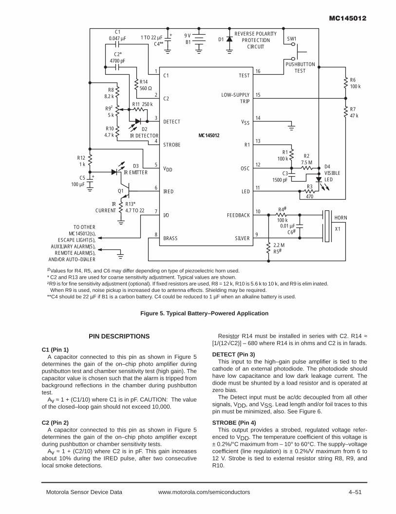
4–51Motorola Sensor Device Data www.motorola.com/semiconductors
16
15
14
13
12
11
10
9
1
2
3
4
5
6
7
8
TEST
LOW–SUPPLYTRIP
VSS
R1
OSC
LED
FEEDBACK
SILVER
VDD
IRED
I/O
BRASS
STROBE
DETECT
C1
C2
HORN
X1TO OTHERMC145012(s),
ESCAPE LIGHT(S),AUXILIARY ALARM(S),
REMOTE ALARM(S),AND/OR AUTO–DIALER
IRCURRENT
R13*4.7 TO 22
Q1
2.2 MR5#
D4VISIBLELED
R747 k
R6100 k
SW1+
+
MC145012
REVERSE POLARITYPROTECTION
CIRCUIT
PUSHBUTTONTEST
R27.5 M
0.01 µFC6#
C31500 pF
R1100 k
R3
470
R4#
100 k
9 VB1 D11 TO 22 µF
C4**
C10.047 µF
C2*4700 pF
R14560 Ω
R11 250 k
D2IR DETECTOR
R88.2 k
R9†
5 k
R104.7 k
D3IR EMITTER
R121 k
C5100 µF
#Values for R4, R5, and C6 may differ depending on type of piezoelectric horn used.* C2 and R13 are used for coarse sensitivity adjustment. Typical values are shown.†R9 is for fine sensitivity adjustment (optional). If fixed resistors are used, R8 = 12 k, R10 is 5.6 k to 10 k, and R9 is eliminated.
When R9 is used, noise pickup is increased due to antenna effects. Shielding may be required.**C4 should be 22 µF if B1 is a carbon battery. C4 could be reduced to 1 µF when an alkaline battery is used.
Figure 5. Typical Battery–Powered Application
PIN DESCRIPTIONS
C1 (Pin 1)A capacitor connected to this pin as shown in Figure 5
determines the gain of the on–chip photo amplifier duringpushbutton test and chamber sensitivity test (high gain). Thecapacitor value is chosen such that the alarm is tripped frombackground reflections in the chamber during pushbuttontest.
Av ≈ 1 + (C1/10) where C1 is in pF. CAUTION: The valueof the closed–loop gain should not exceed 10,000.
C2 (Pin 2)A capacitor connected to this pin as shown in Figure 5
determines the gain of the on–chip photo amplifier exceptduring pushbutton or chamber sensitivity tests.
Av ≈ 1 + (C2/10) where C2 is in pF. This gain increasesabout 10% during the IRED pulse, after two consecutivelocal smoke detections.
Resistor R14 must be installed in series with C2. R14 ≈[1/(12√C2)] – 680 where R14 is in ohms and C2 is in farads.
DETECT (Pin 3)This input to the high–gain pulse amplifier is tied to the
cathode of an external photodiode. The photodiode shouldhave low capacitance and low dark leakage current. Thediode must be shunted by a load resistor and is operated atzero bias.
The Detect input must be ac/dc decoupled from all othersignals, VDD, and VSS. Lead length and/or foil traces to thispin must be minimized, also. See Figure 6.
STROBE (Pin 4)This output provides a strobed, regulated voltage refer-
enced to VDD. The temperature coefficient of this voltage is± 0.2%/°C maximum from – 10° to 60°C. The supply–voltagecoefficient (line regulation) is ± 0.2%/V maximum from 6 to12 V. Strobe is tied to external resistor string R8, R9, andR10.

4–52 Motorola Sensor Device Datawww.motorola.com/semiconductors
VDD (Pin 5)This pin is connected to the positive supply potential and
may range from + 6 to + 12 V with respect to VSSCAUTION: In battery–powered applications, reverse–polar-ity protection must be provided externally.
IRED (Pin 6)This output provides pulsed base current for external NPN
transistor Q1 used as the infrared emitter driver. Q1 musthave β ≥ 100. At 10 mA, the temperature coefficient of theoutput voltage is typically + 0.5%/°C from – 10° to 60°C. Thesupply–voltage coefficient (line regulation) is ± 0.2%/V maxi-mum from 6 to 12 V. The IRED pulse width (active–high) isdetermined by external components R1 and C3. With a100 kΩ/1500 pF combination, the nominal width is 105 µs.
To minimize noise impact, IRED is not active when the vis-ible LED and horn outputs are active. IRED is active near theend of strobe pulses for smoke tests, chamber sensitivitytest, and pushbutton test.
I/O (Pin 7)This pin can be used to connect up to 40 units together in
a wired–OR configuration for common signaling. VSS is usedas the return. An on–chip current sink minimizes noise pickup during non–smoke conditions and eliminates the need foran external pull–down resistor to complete the wired–OR.Remote units at lower supply voltages do not draw excessivecurrent from a sending unit at a higher supply voltage.
I/O can also be used to activate escape lights, auxiliaryalarms, remote alarms, and/or auto–dialers.
As an input, this pin feeds a positive–edge–triggered flip–flop whose output is sampled nominally every 1 second dur-ing standby (using the recommended component values). Alocal–smoke condition or the pushbutton–test mode forcesthis current–limited output to source current. All input signalsare ignored when I/O is sourcing current.
I/O is disabled by the on–chip power–on reset to eliminatenuisance signaling during battery changes or system power–up.
If unused, I/O must be left unconnected.
BRASS (Pin 8)This half of the push–pull driver output is connected to the
metal support electrode of a piezoelectric audio transducerand to the horn–starting resistor. A continuous modulatedtone from the transducer is a smoke alarm indicating eitherlocal or remote smoke. A short beep or chirp is a troublealarm indicating a low supply or degraded chamber sensitiv-ity.
SILVER (Pin 9)This half of the push–pull driver output is connected to the
ceramic electrode of a piezoelectric transducer and to thehorn–starting capacitor.
FEEDBACK (Pin 10)This input is connected to both the feedback electrode of a
self–resonating piezoelectric transducer and the horn–start-ing resistor and capacitor through current–limiting resistorR4. If unused, this pin must be tied to VSS or VDD.
LED (Pin 11)This active–low open–drain output directly drives an exter-
nal visible LED at the pulse rates indicated below. The pulsewidth is equal to the OSC period.
The load for the low–supply test is applied by this output.This low–supply test is non–coincident with the smoke tests,chamber sensitivity test, pushbutton test, or any alarm sig-nals.
The LED also provides a visual indication of the detectorstatus as follows, assuming the component values shown inFigure 5:
Standby (includes low–supply and chamber sensitivitytests) — Pulses every 32.4 seconds (typical)
Local Smoke — Pulses every 0.51 seconds (typical)
Remote Smoke — No pulses
Pushbutton Test — Pulses every 0.51 seconds (typical)
OSC (Pin 12)This pin is used in conjunction with external resistor R2
(7.5 MΩ) to VDD and external capacitor C3 (1500 pF) to VDDto form an oscillator with a nominal period of 7.9 ms (typical).
R1 (Pin 13)This pin is used in conjunction with resistor R1 (100 kΩ) to
Pin 12 and C3 (1500 pF, see Pin 12 description) to determinethe IRED pulse width. With this RC combination, the nominalpulse width is 105 µs.
VSS (Pin 14)This pin is the negative supply potential and the return for
the I/O pin. Pin 14 is usually tied to ground.
LOW–SUPPLY TRIP (Pin 15)This pin is connected to an external voltage which deter-
mines the low–supply alarm threshold. The trip voltage isobtained through a resistor divider connected between theVDD and LED pins. The low–supply alarm threshold voltage(in volts) ≈ (5R7/R6) + 5 where R6 and R7 are in the sameunits.
TEST (Pin 16)This input has an on–chip pull–down device and is used to
manually invoke a test mode.The Pushbutton Test mode is initiated by a high level at Pin
16 (usually depression of a S.P.S.T. normally–open pushbut-ton switch to VDD). After one oscillator cycle, IRED pulsesapproximately every 1.0 second, regardless of the presenceof smoke. Additionally, the amplifier gain is increased byautomatic selection of C1. Therefore, the background reflec-tions in the smoke chamber may be interpreted as smoke,generating a simulated–smoke condition. After the secondIRED pulse, a successful test activates the horn–driver andI/O circuits. The active I/O allows remote signaling for systemtesting. When the Pushbutton Test switch is released, theTest input returns to VSS due to the on–chip pull–downdevice. After one oscillator cycle, the amplifier gain returns tonormal, thereby removing the simulated–smoke condition.After two additional IRED pulses, less than three seconds,the IC exits the alarm mode and returns to standby timing.

4–53Motorola Sensor Device Data www.motorola.com/semiconductors
CALIBRATION
To facilitate checking the sensitivity and calibrating smokedetectors, the MC145012 can be placed in a calibrationmode. In this mode, certain device pins are controlled/recon-figured as shown in Table 1. To place the part in the calibra-
tion mode, Pin 16 (Test) must be pulled below the VSS pinwith 100 µA continuously drawn out of the pin for at least onecycle on the OSC pin. To exit this mode, the Test pin isfloated for at least one OSC cycle.
In the calibration mode, the IRED pulse rate is increased toone for every OSC cycle. Also, Strobe is always active low.
Table 1. Configuration of Pins in the Calibration Mode
Description Pin Comment
I/O 7 Disabled as an output. Forcing this pin high places the photo amp output on Pin 1 or 2, as determined byLow–Supply Trip. The amp’s output appears as pulses and is referenced to VDD etc.
Low–Supply Trip 15 If the I/O pin is high, Pin 15 controls which gain capacitor is used. Low: normal gain, amp output on Pin 1.High: supervisory gain, amp output on Pin 2.
Feedback 10 Driving this input high enables hysteresis (10% gain increase) in the photo amp; Pin 15 must be low.
OSC 12 Driving this input high brings the internal clock high. Driving the input low brings the internal clock low. Ifdesired, the RC network for the oscillator may be left intact; this allows the oscillator to run similar to thenormal mode of operation.
Silver 9 This pin becomes the smoke comparator output. When the OSC pin is toggling, positive pulses indicatethat smoke has been detected. A static low level indicates no smoke.
Brass 8 This pin becomes the smoke integrator output. That is, 2 consecutive smoke detections are required for“on” (static high level) and 2 consecutive no–detections for “off” (static low level).
NOTES: Illustration is bottom view of layout using a DIP. Top view for SOIC layout is mirror image.Optional potentiometer R9 is not included.Drawing is not to scale.Leads on D2, R11, R8, and R10 and their associated traces must be kept as short as possible.
This practice minimizes noise pick up. Pin 3 must be decoupled from all other traces.
Figure 6. Recommended PCB Layout
DO NOT RUN ANYADDITIONAL TRACES
IN THIS REGION
PIN 8
PIN 16
PIN 9
PIN 1
C1
R14
R11
D2
R8
MOUNTED INCHAMBER
C2
R10

4–54 Motorola Sensor Device Datawww.motorola.com/semiconductors
Low–Power CMOS" !
The MC145017, when used with an ionization chamber and a small number ofexternal components, will detect smoke. When smoke is sensed, an alarm is soundedvia an external piezoelectric transducer and internal drivers. This circuit is designed tooperate in smoke detector systems that comply with UL217 and UL268 specifications.
• Ionization Type with On–Chip FET Input Comparator
• Piezoelectric Horn Driver
• Guard Outputs on Both Sides of Detect Input
• Input–Production Diodes on the Detect Input
• Low–Battery Trip Point, Internally Set, can be Altered Via External Resistor
• Detect Threshold, Internally Set, can be Altered Via External Resistor
• Pulse Testing for Low Battery Uses LED for Battery Loading
• Comparator Outputs for Detect and Low Battery
• Internal Reverse Battery Protection
• Supports NFPA 72, ANSi 53.41, and ISO 8201Audible Emergency Evacuation Signals
MAXIMUM RATINGS* (Voltages referenced to VSS)
Rating Symbol Value Unit
DC Supply Voltage VDD 0.5 to + 15 V
Input Voltage, All Inputs Except Pin 8 Vin 0.25 to VDD + 0.25 V
DC Current Drain per Input Pin, Except Pin 15 = 1 mA I 10 mA
DC Current Drain per Output Pin I 30 mA
Operating Temperature Range TA 10 to + 60 °C
Storage Temperature Range Tstg 55 to + 125 °C
Reverse Battery Time tRB 5.0 s
* Maximum Ratings are those values beyond which damage to the device may occur.
This device contains circuitry to protect the inputs against damage due to high static voltages or electric fields; however, it is advised that normalprecautions be taken to avoid application of any voltage higher than maximum rated voltages to this high impedance circuit. For proper operationit is recommended that Vin and Vout be constrained to the range VSS (Vin or Vout) VDD.
SEMICONDUCTOR TECHNICAL DATA
P SUFFIXPLASTIC DIPCASE 648–08
PIN ASSIGNMENT(16 PIN DIP)
16
15
14
13
12
11
10
9
1
2
3
4
5
6
7
8
DetectComp. Out
N/C
Low V Set
Low VComp. Out
LED
VDD
TimingResistor
Feedback
Guard Hi–Z
Detect Input
Guard Lo–Z
Sensitivity Set
Osc Capacitor
Silver
Brass
VSS
ORDERING INFORMATION
MC145017P PLASTIC DIP
1
16
REV 4
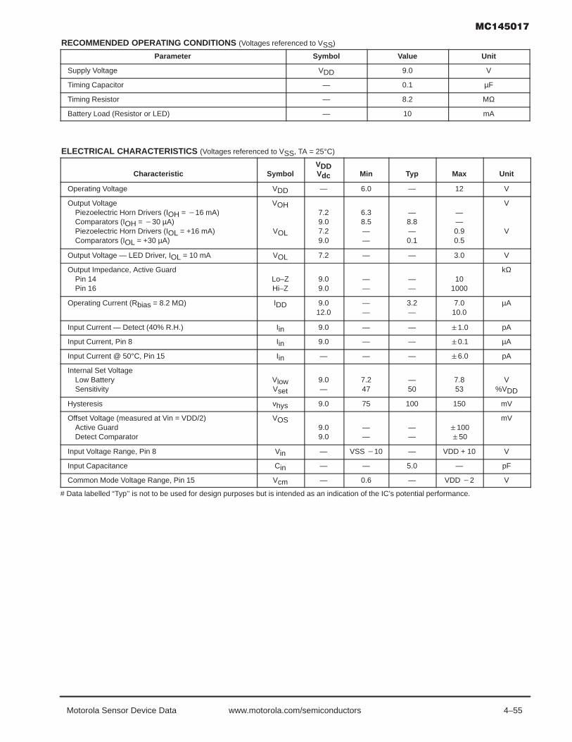
4–55Motorola Sensor Device Data www.motorola.com/semiconductors
RECOMMENDED OPERATING CONDITIONS (Voltages referenced to VSS)
Parameter Symbol Value Unit
Supply Voltage VDD 9.0 V
Timing Capacitor — 0.1 µF
Timing Resistor — 8.2 MΩ
Battery Load (Resistor or LED) — 10 mA
ELECTRICAL CHARACTERISTICS (Voltages referenced to VSS, TA = 25°C)
Characteristic SymbolVDDVdc Min Typ Max Unit
Operating Voltage VDD — 6.0 — 12 V
Output VoltagePiezoelectric Horn Drivers (IOH = 16 mA)Comparators (IOH = 30 µA)Piezoelectric Horn Drivers (IOL = +16 mA)Comparators (IOL = +30 µA)
VOH
VOL
7.29.07.29.0
6.38.5——
—8.8—0.1
——0.90.5
V
V
Output Voltage — LED Driver, IOL = 10 mA VOL 7.2 — — 3.0 V
Output Impedance, Active GuardPin 14Pin 16
Lo–ZHi–Z
9.09.0
——
——
101000
kΩ
Operating Current (Rbias = 8.2 MΩ) IDD 9.012.0
——
3.2—
7.010.0
µA
Input Current — Detect (40% R.H.) Iin 9.0 — — 1.0 pA
Input Current, Pin 8 Iin 9.0 — — 0.1 µA
Input Current @ 50°C, Pin 15 Iin — — — 6.0 pA
Internal Set VoltageLow BatterySensitivity
VlowVset
9.0—
7.247
—50
7.853
V%VDD
Hysteresis vhys 9.0 75 100 150 mV
Offset Voltage (measured at Vin = VDD/2)Active GuardDetect Comparator
VOS9.09.0
——
——
10050
mV
Input Voltage Range, Pin 8 Vin — VSS 10 — VDD + 10 V
Input Capacitance Cin — — 5.0 — pF
Common Mode Voltage Range, Pin 15 Vcm — 0.6 — VDD 2 V
# Data labelled “Typ’’ is not to be used for design purposes but is intended as an indication of the IC’s potential performance.

4–56 Motorola Sensor Device Datawww.motorola.com/semiconductors
TIMING PARAMETERS (C = 0.1 µF, Rbias = 8.2 MΩ, VDD = 9.0 V, TA = 25°C, See Figure 6)
Characteristics Symbol Min Max Units
Oscillator Period No SmokeSmoke
tCI 1.4637.5
1.8545.8
sms
Oscillator Rise Time tr 10.1 12.3 ms
Horn Output On Time(During Smoke) Off Time
PWonPWoff
450450
550550
msms
LED Output BetweenPulses On Time
tLEDPWon
35.010.1
44.512.3
sms
Horn Output On Time(During Low Battery) BetweenPulses
tontoff
10.135.0
12.344.5
mss
Figure 1. Block Diagram
+
–
VDD
LATCH
LOW BATTERY COMP.
OSCILLATORTIMER
LATCH+
–
VDD
80 K
3
1045 K
7
12
1
13
1125 K
+
–
15
DETECT INPUT
14 LO–Z
ACTIVEGUARD
16 HI–Z
VDD
4
VDD
8
PIEZOELECTRICHORN DRIVER
11
10
5
LED DRIVER
VDD
69

4–57Motorola Sensor Device Data www.motorola.com/semiconductors
Figure 2. Typical LED Output I–V Characteristic
Figure 3. Typical Comparator Output I–V Characteristic
Figure 4. Typical P Horn Driver Output I–V Characteristic
0 1 2 3 4 5 6 7 8 9 100.1
1.0
10.0
100.0
TA = 25°C
VDS, DRAIN TO SOURCE VOLTAGE (Vdc)
VDD = 7.2 Vdc
VDD = 9.0 Vdc
0 1 2 3 4 5 6 7 8 9 101.0
10.0
100.0
1000.0
DI ,
DR
AIN
CU
RR
ENT
(mA)
TA = 25°C
VDS, DRAIN TO SOURCE VOLTAGE (Vdc)
P–CH SOURCE CURRENT
VDD = 7.2 Vdc
VDD = 9.0 Vdc
0 1 2 3 4 5 6 7 8 9 101.0
10.0
100.0
1000.0
DI ,
DR
AIN
CU
RR
ENT
(mA)
TA = 25°C
VDS, DRAIN TO SOURCE VOLTAGE (Vdc)
N–CH SINK CURRENT
VDD = 7.2 Vdc
VDD = 9.0 Vdc
0 1 2 3 4 5 6 7 8 9 100.01
0.1
1.0
10.0
DI ,
DR
AIN
CU
RR
ENT
(mA)
TA = 25°C
VDS, DRAIN TO SOURCE VOLTAGE (Vdc)
P–CH SOURCEAND N–CH
SINK CURRENT
VDD = 9.0 Vdc or 7.2 Vdc
DI ,
DR
AIN
CU
RR
ENT
(mA)

4–58 Motorola Sensor Device Datawww.motorola.com/semiconductors
DEVICE OPERATION
TIMINGThe internal oscillator of the MC145017 operates with a
period of 1.65 seconds during no–smoke conditions. Each1.65 seconds, internal power is applied to the entire IC and acheck is made for smoke, except during LED pulse, Low Bat-tery Alarm Chirp, or Horn Modulation (in smoke). Every 24clock cycles a check is made for low battery by comparingVDD to an internal zener voltage. Since very small currentsare used in the oscillator, the oscillator capacitor should be ofa low leakage type.
DETECT CIRCUITRYIf smoke is detected, the oscillator period becomes
41.67 ms and the piezoelectric horn oscillator circuit isenabled. The horn output is modulated 500 ms on, 500 msoff. During the off time, smoke is again checked and will in-hibit further horn output if no smoke is sensed. During smokeconditions the low battery alarm is inhibited, but the LEDpulses at a 1.0 Hz rate.
An active guard is provided on both pins adjacent to thedetect input. The voltage at these pins will be within 100 mVof the input signal. This will keep surface leakage currents toa minimum and provide a method of measuring the input volt-age without loading the ionization chamber. The active guardop amp is not power strobed and thus gives constant protec-tion from surface leakage currents. Pin 15 (the Detect input)has internal diode protection against static damage.
SENSITIVITY/LOW BATTERY THRESHOLDSBoth the sensitivity threshold and the low battery voltage
levels are set internally by a common voltage divider (please
see Figure 1) connected between VDD and VSS. These volt-ages can be altered by external resistors connected frompins 3 or 13 to either VDD or VSS. There will be a slight inter-action here due to the common voltage divider network. Thesensitivity threshold can also be set by adjusting the smokechamber ionization source.
TEST MODESince the internal op amps and comparators are power
strobed, adjustments for sensitivity or low battery level couldbe difficult and/or time–consuming. By forcing Pin 12 to VSS,the power strobing is bypassed and the outputs, Pins 1 and4, constantly show smoke/no smoke and good battery/lowbattery, respectively. Pin 1 = VDD for smoke and Pin 4 = VDDfor low battery. In this mode and during the 10 ms powerstrobe, chip current rises to approximately 50 µA.
LED PULSEThe 9–volt battery level is checked every 40 seconds dur-
ing the LED pulse. The battery is loaded via a 10 mA pulsefor 11.6 ms. If the LED is not used, it should be replaced withan equivalent resistor such that the battery loading remainsat 10 mA.
HYSTERESISWhen smoke is detected, the resistor/divider network that
sets sensitivity is altered to increase sensitivity. This yieldsapproximately 100 mV of hysteresis and reduces falsetriggering.
Figure 5. Typical Application as Ionization Smoke Detector
MC1450171 16
2
3
4
5
6
7
8
15
14
13
12
11
10
9
330 Ω
8.2 MΩ+
9 V0.1 µF
1.5 MΩ*0.001 µF 220 kΩ*
0.1 µF
1 M 1 M
TEST
*NOTE: Component values may change depending on type of piezoelectric horn used.

4–59Motorola Sensor Device Data www.motorola.com/semiconductors
Figure 6. MC145017 Timing Diagram
OSCPIN 12
SMOKE – N– Y
LOW BAT – Y– N
HYSTPIN 13
HORN – ON– OFF
LED – OFF– ON
2 3 4 5 6 7 98
NO SMOKE, LOW BATTERY
1
NO SMKNO LOW BAT
LOW BATTERY CHIRP
OSCPIN 12
SMOKE – N– Y
NO SMK
23 24 1 6 12 18 24
SMOKE
LATCH ALARM CONDITION
(100 mV LEVEL SHIFT)
NFPA MOD
LOW BAT – Y– N
HORN – ON– OFF
LED – OFF– ON
(NOTE 1)
24 CLOCKS 24 CLOCKS
NOTES:1. Horn modulation is self–completing. When going from smoke to no smoke, the alarm condition will terminate only when horn is off.2. Comparators are strobed once per cycle (1.65 sec for no smoke, 40 msec for smoke).
Figure 7. Horn Modulation
NFPA72: TEMPORAL HORNMODULATION PATTERN
TRADITIONAL 4/6 HORNMODULATION PATTERN
0.5 SEC0.5 SEC
0.5 SEC0.5 SEC
0.5 SEC 1.5 SEC
167 msec83 msec

4–60 Motorola Sensor Device Datawww.motorola.com/semiconductors
Low–Power CMOS" !
The MC145018, when used with an ionization chamber and a small number ofexternal components, will detect smoke. When smoke is sensed, an alarm is soundedvia an external piezoelectric transducer and internal drivers. This circuit is designed tooperate in smoke detector systems that comply with UL217 and UL268 specifications.
• Ionization Type with On–Chip FET Input Comparator
• Piezoelectric Horn Driver
• Guard Outputs on Both Sides of Detect Input
• Input–Protection Diodes on the Detect Input
• Low–Battery Trip Point, Internally Set, can be Altered Via External Resistor
• Detect Threshold, Internally Set, can be Altered Via External Resistor
• Pulse Testing for Low Battery Uses LED for Battery Loading
• Comparator Output for Detect
• Internal Reverse Battery Protection
• Strobe Output for External Trim Resistors
• I/O Pin Allows Up to 40 Units to be Connected for Common Signaling
• Supports NFPA 72, ANSi 53.41, and ISO 8201Audible Emergency Evacuation Signals
• Power–On Reset Places IC in Standby Mode
MAXIMUM RATINGS* (Voltages referenced to VSS)
Rating Symbol Value Unit
DC Supply Voltage VDD 0.5 to + 15 V
Input Voltage, All Inputs Except Pin 8 Vin 0.25 to VDD + 0.25 V
DC Current Drain per Input Pin, Except Pin 15 = 1 mA I 10 mA
DC Current Drain per Output Pin I 30 mA
Operating Temperature Range TA 10 to + 60 °C
Storage Temperature Range Tstg 55 to + 125 °C
Reverse Battery Time tRB 5.0 s
* Maximum Ratings are those values beyond which damage to the device may occur.
This device contains circuitry to protect the inputs against damage due to high static voltages or electric fields; however, it is advised that normalprecautions be taken to avoid application of any voltage higher than maximum rated voltages to this high impedance circuit. For proper operationit is recommended that Vin and Vout be constrained to the range VSS (Vin or Vout) VDD.
SEMICONDUCTOR TECHNICAL DATA
P SUFFIXPLASTIC DIPCASE 648–08
PIN ASSIGNMENT(16 PIN DIP)
16
15
14
13
12
11
10
9
1
2
3
4
5
6
7
8
DetectComp. Out
I/O
Low V Set
Strobe Out
LED
VDD
TimingResistor
Feedback
Guard Hi–Z
Detect Input
Guard Lo–Z
Sensitivity Set
Osc Capacitor
Silver
Brass
VSS
ORDERING INFORMATION
MC145018P PLASTIC DIP
1
16
REV 3

4–61Motorola Sensor Device Data www.motorola.com/semiconductors
RECOMMENDED OPERATING CONDITIONS (Voltages referenced to VSS)
Parameter Symbol Value Unit
Supply Voltage VDD 9.0 V
Timing Capacitor — 0.1 µF
Timing Resistor — 8.2 MΩ
Battery Load (Resistor or LED) — 10 mA
ELECTRICAL CHARACTERISTICS (Voltages referenced to VSS, TA = 25°C)
Characteristic SymbolVDDVdc Min Typ Max Unit
Operating Voltage VDD — 6.0 — 12 V
Output VoltagePiezoelectric Horn Drivers (IOH = 16 mA)Comparators (IOH = 30 µA)Piezoelectric Horn Drivers (IOL = + 16 mA)Comparators (IOL = +30 µA)
VOH
VOL
7.29.07.29.0
6.38.5——
—8.8—0.1
——0.90.5
V
V
Output Voltage — LED Driver, IOL = 10 mA VOL 7.2 — — 3.0 V
Output Impedance, Active GuardPin 14Pin 16
Lo–ZHi–Z
9.09.0
——
——
101000
kΩ
Operating Current (Rbias = 8.2 MΩ) IDD 9.012.0
——
5.0—
9.012.0
µA
Input Current — Detect (40% R.H.) Iin 9.0 — — 1.0 pA
Input Current, Pin 8 Iin 9.0 — — 0.1 µA
Input Current @ 50°C, Pin 15 Iin — — — 6.0 pA
Internal Set VoltageLow BatterySensitivity
VlowVset
9.0—
7.247
—50
7.853
V%VDD
Hysteresis vhys 9.0 75 100 150 mV
Offset Voltage (measured at Vin = VDD/2)Active GuardDetect Comparator
VOS9.09.0
——
——
10050
mV
Input Voltage Range, Pin 8 Vin — VSS 10 — VDD + 10 V
Input Capacitance Cin — — 5.0 — pF
Common Mode Voltage Range, Pin 15 Vcm — 0.6 — VDD 2 V
I/O Current, Pin 2Input, VIH = VDD 2Output, VOH = VDD 2
IIHIOH
——
254.0
——
10016
µAmA
# Data labelled “Typ’’ is not to be used for design purposes but is intended as an indication of the IC’s potential performance.
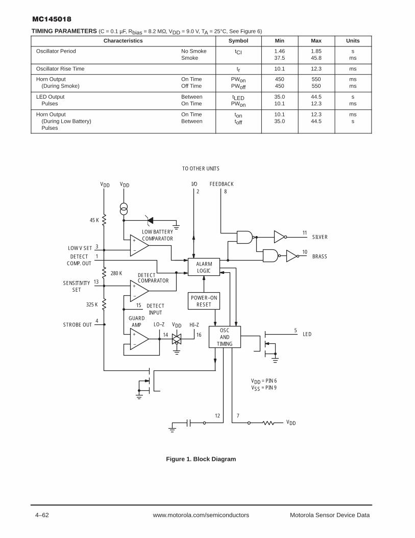
4–62 Motorola Sensor Device Datawww.motorola.com/semiconductors
TIMING PARAMETERS (C = 0.1 µF, Rbias = 8.2 MΩ, VDD = 9.0 V, TA = 25°C, See Figure 6)
Characteristics Symbol Min Max Units
Oscillator Period No SmokeSmoke
tCI 1.4637.5
1.8545.8
sms
Oscillator Rise Time tr 10.1 12.3 ms
Horn Output On Time(During Smoke) Off Time
PWonPWoff
450450
550550
msms
LED Output BetweenPulses On Time
tLEDPWon
35.010.1
44.512.3
sms
Horn Output On Time(During Low Battery) BetweenPulses
tontoff
10.135.0
12.344.5
mss
LOW BATTERYCOMPARATOR
Figure 1. Block Diagram
VDD
45 K
3LOW V SET
1DETECTCOMP. OUT
280 K
13SENSITIVITYSET
325 K
STROBE OUT4
VDD
+
–
+
–
15 DETECTINPUT
DETECTCOMPARATOR
GUARDAMP
+
–
LO–Z
14 16
ALARMLOGIC
POWER–ONRESET
OSCAND
TIMING
I/O2
11
FEEDBACK8
10
SILVER
BRASS
5LED
VDD = PIN 6VSS = PIN 9
12 7VDD
TO OTHER UNITS
HI–ZVDD

4–63Motorola Sensor Device Data www.motorola.com/semiconductors
0 1 2 3 4 5 6 7 8 9 100.1
1.0
10.0
100.0
TA = 25°C
VDS, DRAIN TO SOURCE VOLTAGE (Vdc)
VDD = 7.2 Vdc
VDD = 9.0 Vdc
0 1 2 3 4 5 6 7 8 9 101.0
10.0
100.0
1000.0
DI ,
DR
AIN
CU
RR
ENT
(mA)
TA = 25°C
VDS, DRAIN TO SOURCE VOLTAGE (Vdc)
P–CH SOURCE CURRENT
VDD = 7.2 Vdc
VDD = 9.0 Vdc
0 1 2 3 4 5 6 7 8 9 101.0
10.0
100.0
1000.0
DI ,
DR
AIN
CU
RR
ENT
(mA)
TA = 25°C
VDS, DRAIN TO SOURCE VOLTAGE (Vdc)
N–CH SINK CURRENT
VDD = 7.2 Vdc
VDD = 9.0 Vdc
0 1 2 3 4 5 6 7 8 9 100.01
0.1
1.0
10.0
DI ,
DR
AIN
CU
RR
ENT
(mA)
TA = 25°C
VDS, DRAIN TO SOURCE VOLTAGE (Vdc)
P–CH SOURCEAND N–CH
SINK CURRENT
VDD = 9.0 Vdc or 7.2 Vdc
DI ,
DR
AIN
CU
RR
ENT
(mA)
Figure 2. Typical LED Output I–V Characteristic
Figure 3. Typical Comparator Output I–V Characteristic
Figure 4. Typical P Horn Driver Output I–V Characteristic

4–64 Motorola Sensor Device Datawww.motorola.com/semiconductors
DEVICE OPERATION
TIMINGThe internal oscillator of the MC145018 operates with a
period of 1.65 seconds during no–smoke conditions. Each1.65 seconds, internal power is applied to the entire IC and acheck is made for smoke, except during LED pulse, Low Bat-tery Alarm Chirp, or Horn Modulation (in smoke). Every 24clock cycles a check is made for low battery by comparingVDD to an internal zener voltage. Since very small currentsare used in the oscillator, the oscillator capacitor should be ofa low leakage type.
DETECT CIRCUITRYIf smoke is detected, the oscillator period becomes
41.67 ms and the piezoelectric horn oscillator circuit isenabled. The horn output is modulated 500 ms on, 500 msoff. During the off time, smoke is again checked and willinhibit further horn output if no smoke is sensed. During localsmoke conditions the low battery alarm is inhibited, but theLED pulses at a 1.0 Hz rate. In remote smoke, the LED isinhibited as well.
An active guard is provided on both pins adjacent to thedetect input. The voltage at these pins will be within 100 mVof the input signal. This will keep surface leakage currents toa minimum and provide a method of measuring the input volt-age without loading the ionization chamber. The active guardop amp is not power strobed and thus gives constant protec-tion from surface leakage currents. Pin 15 (the Detect input)has internal diode protection against static damage.
INTERCONNECTThe I/O (Pin 2), in combination with VSS, is used to inter-
connect up to 40 remote units for common signaling. A LocalSmoke condition activates a current limited output driver,thereby signaling Remote Smoke to interconnected units. Asmall current sink improves noise immunity during non–smoke conditions. Remote units at lower voltages do not
draw excessive current from a sending unit at a higher volt-age. The I/O is disabled for three oscillator cycles after powerup, to eliminate false alarming of remote units when the bat-tery is changed.
SENSITIVITY/LOW BATTERY THRESHOLDSBoth the sensitivity threshold and the low battery voltage
levels are set internally by a common voltage divider (seeFigure 1) connected between VDD and VSS. These voltagescan be altered by external resistors connected from pins 3 or13 to either VDD or VSS. There will be a slight interaction heredue to the common voltage divider network. The sensitivitythreshold can also be set by adjusting the smoke chamberionization source.
TEST MODESince the internal op amps and comparators are power
strobed, adjustments for sensitivity or low battery level couldbe difficult and/or time–consuming. By forcing Pin 12 to VSS,the power strobing is bypassed and the output, Pin 1,constantly shows smoke/no smoke. Pin 1 = VDD for smoke.In this mode and during the 10 ms power strobe, chip currentrises to approximately 50 µA.
LED PULSEThe 9–volt battery level is checked every 40 seconds dur-
ing the LED pulse. The battery is loaded via a 10 mA pulsefor 11.6 ms. If the LED is not used, it should be replaced withan equivalent resistor such that the battery loading remainsat 10 mA.
HYSTERESISWhen smoke is detected, the resistor/divider network that
sets sensitivity is altered to increase sensitivity. This yieldsapproximately 100 mV of hysteresis and reduces falsetriggering.
Figure 5. Typical Application as Ionization Smoke Detector
TOOTHERUNITS
MC1450181 16
2
3
4
5
6
7
8
15
14
13
12
11
10
9
330 Ω
8.2 MΩ+
9 V0.1 µF
1.5 MΩ*0.001 µF 220 kΩ*
0.1 µF
1 M 1 M
TEST
*NOTE: Component values maychange depending on type ofpiezoelectric horn used.

4–65Motorola Sensor Device Data www.motorola.com/semiconductors
Figure 6. MC145018 Timing Diagram
OSCPIN 12
SMOKE – N– Y
LOW BAT – Y– N
HYSTPIN 13
HORN – ON– OFF
LED – OFF– ON
2 3 4 5 6 7 98
NO SMOKE, LOW BATTERY
1
NO SMKNO LOW BAT
LOW BATTERY CHIRP
OSCPIN 12
SMOKE – N– Y
NO SMK
23 24 1 6 12 18 24
SMOKE
LATCH ALARM CONDITION
(100 mV LEVEL SHIFT)
NFPA MOD
LOW BAT – Y– N
HORN – ON– OFF
LED – OFF– ON
(NOTE 1)
24 CLOCKS 24 CLOCKS
NOTES:1. Horn modulation is self–completing. When going from smoke to no smoke, the alarm condition will terminate only when horn is off.2. Comparators are strobed once per cycle (1.65 sec for no smoke, 40 msec for smoke).3. For timing under remote conditions, refer to MC14468 data sheet.
Figure 7. Horn Modulation
NFPA72: TEMPORAL HORNMODULATION PATTERN
TRADITIONAL 4/6 HORNMODULATION PATTERN
0.5 SEC0.5 SEC
0.5 SEC0.5 SEC
0.5 SEC 1.5 SEC
167 msec83 msec

4–66 Motorola Sensor Device Datawww.motorola.com/semiconductors
Prepared by: Leticia Gomez and Diana PelletierSensor Applications EngineeringMotorola Semiconductor Products SectorPhoenix, Arizona
INTRODUCTION
The MC14600, an IC designed for alarm applications, is aversatile part that can easily be configured with a minimumnumber of external components to serve a wide range of alarmapplications and circuit configurations. For example, theMC14600 can be used in systems that detect pressure andtemperature change, liquid levels, motion or intrusion. Thisapplication note presents considerations in interfacing exter-nal components to the MC14600 and an approach for config-uring it with a latch.
The MC14600 Alarm IC can be simply described as acomparator that determines whether an alarm condition existsand in response drives a piezo horn. As illustrated in Figure 1the MC14600 is more than a comparator and a horn driver. Itdrives an LED to indicate the device is working and has inter-nal low battery detection circuitry. In the event of a low batterythe MC14600 provides the signal to chirp the piezo horn. It
also has a logical output that can be used to drive other out-puts such as an LED. The MC14600 alarm threshold andoscillator speed are set externally providing system designflexibility. Figure 2 is a detailed block diagram of the MC14600that includes the pin numbers referenced in this document.
Figure 1. Alarm IC Concept
INPUT +
–ALARM THRESHOLD
LOW BATTERYDETECTION LOGICAL OUTPUT
PIEZO HORN
LED
Figure 2. MC14600 Block Diagram
11
10
8HORN FEEDBACK
HORNOUT 2
HORNOUT 1
ALARMLOGIC
OSCAND
TIMING
5LED
VDD = PIN 6VSS = PIN 9
7VDD
+
–
LOW BATTERYCOMPARATOR
VDDLOW V COMP.
OUT4
VDD
3LOW V SET
1DETECT
COMPARATOR OUT
+
–13
DETECTCOMPARATORALARM
THRESHOLD
15ALARM DETECTINPUT
+
–
VDD HI–Z
16
GUARDAMP
12Cosc Rbias
SEMICONDUCTOR APPLICATION NOTE
REV 3

4–67Motorola Sensor Device Data www.motorola.com/semiconductors
ALARM THRESHOLD ADJUSTMENTS
The alarm trigger point (alarm threshold) is set externally toany voltage level with a simple voltage divider connected topin 13. For instance, to connect the Alarm IC to a sensor thathas an output of 1.0 V during a no alarm condition and 4.0 Vduring an alarm condition, the alarm threshold voltage couldbe set to 3.0 V using a 2 MΩ and a 1 MΩ resistor connectedbetween VDD and ground (See Figure 3). Pin 13 connectsinternally to the negative input of the Detect Comparator.Based on the input impedance of the Detect Comparator themaximum suggested total resistance for the threshold voltagedivider is 10 MΩ.
Figure 3. Alarm Threshold Voltage Divider
VDD
2 M
1 M
PIN 13
OSCILLATOR
The master clock frequency for the MC14600 is determinedby the external components Rbias (pin 7) and Cosc (pin 12).This RC network provides the timing for the various functionsconducted by the IC. The oscillator timing affects the periodbetween LED pulses, alarm signal sampling, and the horn out-put pulses and power consumption. A standard RC networkfor the MC14600 oscillator uses an 8.2 M resistor (Rbias) con-nected from VDD to pin 7 and a 0.1 uF capacitor (Cosc) con-nected from pin 12 to ground. This configuration will providea period of approximately 1.65 sec in standby and 41.67 msecin alarm. A change in oscillator speed is accomplished bychanging the resistor and capacitor values previously stated.Changing the oscillator timing will not change the horn patternbut it will change the speed at which it’s delivered. The tablebelow lists examples of RC values and measured samplingperiods achieved with those values (deviation from theoreticalvalues are due to tolerance in components).
Table 1. Oscillator Period vs. R bias and Cosc Value
Rbias Cosc Period (no alarm) Period (alarm)
5.6 MΩ 0.01 µF 93 msec 2.3 msec
8.2 MΩ 0.01 µF 142 msec 3.4 msec
10 MΩ 0.01 µF 172 msec 3.9 msec
5.6 MΩ 0.1 µF 1.4 sec 32 msec
8.2 MΩ 0.1 µF 2.2 sec 50 msec
10 MΩ 0.1 µF 2.7 sec 60 msec
8.2 MΩ 1.0 µF 20.1 sec 456 msec
PIEZO HORN INTERFACE
The MC14600 contains on–board horn driver circuitry todrive three leaded piezo horns. A three leaded horn is consid-ered self–driven, having a feedback pin that is connected toa closed loop oscillation circuit. The MC14600 uses pin 8(Horn Feedback), pin 10 (Horn Out 1) and pin 11 (Horn Out 2)to interface to a piezo horn and achieve the drive circuit. Pin10 and pin 11 alternate their output providing the oscillation forthe horn. Three external components are required to interfacea piezo horn to the Alarm IC: R1, C1 and R2 (Figure 4). R1 isusually around 1.5 MΩ and is the least critical component asit only biases the horn. R2 and C1 are critical to achieve maxi-mum horn output. The two components must be set so that thevalue of 1/(R2*C1) is close to the resonant frequency of thehorn being used. Table 2 lists a common horn frequency andpotential external components that can be used for R2 and C1.
Figure 4. Piezo Horn Interface to MC14600
FDBK
8
R2R1
C1
11OUT 2
ALARM LOGIC
10OUT 1
Table 2. External Components for a 3.4 kHzThree Leaded Piezo Horn
Horn Osc.Frequency R1 R2 C1 1/(R2*C1)
3.4 0.4 kHz 1.5 MΩ820 kΩ1.5 MΩ1.5 MΩ
200 kΩ200 kΩ120 kΩ100 kΩ
1.5 nF1.5 nF2.2 nF2.2 nF
3.33 kHz3.33 kHz3.79 kHz4.55 kHz
LOW BATTERY THRESHOLD ADJUSTMENTSThe Alarm IC has a typical internal low battery reference
voltage of 6 V. An internal resistor divider string provides a volt-age of 80% of VDD which is compared to the 6 V reference volt-age (See Figure 5). This results in a low battery condition andhorn chirp if the VDD level is decreased to approximately 7.5 V.The percentage of VDD that is compared can be changed byadding a resistor to pin 3. A resistor from pin 3 to VDD will lowerthe percentage while a resistor from pin 3 to GND will increasethe percentage. The low battery comparator information willbe latched only during the LED pulse. Testing of the voltageat pin 3 should be done during the LED pulse for confirmation.It should also be measured through a high impedance bufferto avoid altering the voltage level.
ALARM LATCHING APPROACHES
There are detection applications where the event that trig-gers the alarm can be instantaneous, such as shock or motion.

4–68 Motorola Sensor Device Datawww.motorola.com/semiconductors
Figure 5. Low Battery Detection Circuitry
+
–
VDDLOW V COMP. OUT 4
VDD
3LOW V SET
OSC ANDTIMING
In this case the Alarm IC would alarm for the brief moment thatthe event occurred and then stop. This is not always desirable,in particular during events where safety is of concern.
A latch can be implemented using the concept of hystere-sis to alter the alarm threshold level and therefore remain inan alarm condition. It is very simple as it requires only oneresistor, R3, connected to pin 1 (Detect Comp. Out.) andadded in series to the alarm threshold voltage divider, R1 andR2, on pin 13 (See Figure 6). During a no alarm condition pin1 is high which makes the alarm threshold voltage divider looklike it would without R3 connected, keeping the alarm thresh-old at the initial desired point. When an alarm condition occurspin 1 goes low, which in turn dramatically lowers the thresholdvoltage into the alarm comparator. When the alarm signalends and the input voltage into pin 15 decreases, the alarmcondition does not end because the alarm threshold has beenlowered to below a standby voltage level. The MC14600 willcontinue in an alarm condition until the unit is RESET or pin 15receives a signal below this alarming threshold. A RESET isimplemented by connecting a switch to pin 1 that will toggle toVDD through a resistor. This solution has the possibility that itwill not latch on to the alarm condition indefinitely. Asdescribed above it is essentially just lowering the alarmthreshold voltage so if the output from the sensor during a noalarm condition is below this threshold the latch will not work.
SAMPLE DETECTION INPUTS
The MC14600 is a versatile device because its high imped-ence input pin allows it to be connected to a variety of systemsand input signals. All that is required for an input is a device
Figure 6. Latch Using Resistor in Series withThreshold Divider
+
–
ALARM DETECTINPUT (PIN 15)
ALARMTHRESHOLD
R2
R1
13
1
DETECT COMP. OUT
R3
VDD
Internal to MC14600
100 Ω
VDD
RESETSWITCH
or circuit that will produce a change in voltage that corre-sponds to an environmental change. For example, a simplecircuit around a thermistor could cause the MC14600 to alarmwhen the temperature gets too high. A phototransistor couldbe connected to cause an alarm for either the absence or exis-tence of light.
Motorola also has sensors, specifically accelerometersand pressure sensors, that could be used as the input to theMC14600. An accelerometer, such as Motorola’sMMA1201P, could be used to sense a shock or vibration. Apossible solution is shown in Figure 7. The MC7805 is a volt-age regulator that provides the 5 V supply required by theMMA1201P. Since the output of the MMA1201P resulting froma shock or vibration is very short some simple peak detectioncircuitry is required to keep the signal high long enough for theMC14600 to latch onto the alarm condition.
Figure 7. Shock and Vibration Detection Circuit
OUTPUT TOPIN 15 (ALARMDETECT INPUT)
10 M1.0 µF
D1
MMA1201P7805
5 V

4–69Motorola Sensor Device Data www.motorola.com/semiconductors
Motorola’s pressure sensors can also provide the input tothe MC14600. The MPX5000 series includes a wide variety ofcompensated and integrated pressure sensors with differentpressure ranges, packaging and measurement options. Onepossible sensor is the MPXV5010. The output of theMPXV5010 can be fed directly into the input of the MC14600(pin 15). If the latch described above is used with a pressuresensor resistors may be required at the output of theMPXV5010 to scale the output voltage (See Figure 8). This isbecause the output voltage for pressure sensors in theMPX5000 series under no pressure is 0.2 V, which may be be-low the lowered alarm threshold. (See previous section.) Figure 8. Pressure Detection Circuit
VDD
OUTPUT TOPIN 15 (ALARMDETECT INPUT)
MPXV5010
CONCLUSION
The MC14600 offers a simple solution for use in a wide vari-ety of alarm applications. With a high impedance input pin itcan be connected to many types of sensor devices. For sen-sor inputs that require a latched alarm condition there are sev-eral simple ways to add this option to the MC14600. It has thefeature of not having a predetermined alarm threshold which
gives it the flexibility of being set to any level as required by theapplication. The MC14600 has an internal horn driver that candrive a three leaded piezo horn with the addition of two resis-tors and one capacitor. The MC14600 integrates the featuresdesired in alarm devices into a small and simple package thatis still flexible enough for all types of alarm applications.

4–70 Motorola Sensor Device Datawww.motorola.com/semiconductors
Prepared by: Rudi LenzenApplication Engineer, Toulouse France
INTRODUCTIONThe MC14600 is an integrated circuit (IC) designed for
low–cost applications requiring an alarm to be triggered andheard. This device affords the designer a low–cost,easy–to–integrate solution, where board space and designtime are at a premium. The Alarm IC can be used in multipleapplications, such as personal, home and auto safety/securitydevices; door, gate and pool alarms; and even toys, wherelasers and motion are employed, for example. However, thispaper’s purpose is to introduce you to just a few applicationsfor which the MC14600 is a perfect fit.
GAS SENSOR APPLICATIONThe MC14600, used with a flammable gas sensor and a few
added components, provides a reliable solution for gasdetection.
When gas leakage is detected, the sensing resistordecreases typically by a factor 3 or 4 as the gas concentrationreaches 10 percent of the lower explosive limit. During thecalibration sequence (test under gas), a variable resistor isused to set the trigger level of the Alarm IC comparator which,in response, drives a piezo horn.
By adding a thermistor—with negative temperaturecoefficient (NTC) in this case—in the detection circuit, thevariation of the sensor resistance with temperature is easilycompensated, avoiding false alarms when the roomtemperature increases.
–+
R
VSUPPLY
RSENSOR
CALIBRATIONRESISTOR
P15
P13
TH
LOW BATTERYDETECTION
ALARM IC
LED
PIEZO–HORN
LOGICAL
Figure 1. Gas Detection Example
The logical output is useful to signal a remote control stationthat a gas leakage has been detected.
When using a low power sensor, the circuit is fully compliantwith a portable solution enhanced by the integrated lowbattery comparator indicating the state of the power supply.
TEMPERATURE LEVEL DETECTORWhen connected to a simple network of thermistor and
resistors, the Alarm IC provides a portable solution fortemperature control and supervision. The example hereafteruses an NTC thermistor.
An audible alarm will sound when the threshold value at thecomparator input is reached. A logic output is usable forstarting either a fan or a heater depending upon the requiredtemperature.
Figure 2. Temperature Level Example
–+
R
VSUPPLY
P15
P13
TH
LOW BATTERYDETECTION
ALARM IC
LED
PIEZO–HORN
LOGICAL
SEMICONDUCTOR TECHNICAL DATA
REV 0

4–71Motorola Sensor Device Data www.motorola.com/semiconductors
WATER LEVEL DETECTORA single probe connected directly on the detection pin of the
Alarm IC provides a portable solution for water level detection.When liquid enters in contact with the probe, the resistor
between the detection pin and the supply drops from an opencircuit to a measurable value. With an appropriate choice ofbridge resistors, the presence of liquid will trigger thecomparator. The logic level can be connected to anymonitoring system allowing pump starting, floodgate closingand others. This simple system is useful for numerousapplications, such as swimming pool water level alarms,defrosting water level detectors, and in–house flood alarms.
–+
VSUPPLY
PROBE P15
P13
LOW BATTERYDETECTION
ALARM IC
LED
PIEZO–HORN
LOGICAL
Figure 3. Water–Level Detection Example
MOTION INDICATORThe Alarm IC can be used to detect motion and can be
integrated into products, such as an ordinary clothes iron,where this is critical. Used with a low G accelerometer and afew logic components, the device can signal the user thatthere is a risk of clothes burning during use and that the ironmust be shut off from the AC power after use. At the outputof the accelerometer, a simple peak detection circuit isrequired to keep the signal active long enough.
When no movement is detected, the output comparator islow and the counter starts. A first “beep” is heard after a fewseconds to advise that there is a risk of clothes burning. If nomovement is detected, the counting continues and drives aflip–flop connected to pin 15 of the Alarm IC. The alarm istriggered and will continue on until a new movement isdetected, resetting the counter.
–+
VSUPPLY
LOW
GAC
CEL
ERO
MET
ER
P15
LOW BATTERYDETECTION
ALARM IC
LED
PIEZO–HORN
LOGICAL
Figure 4. Motion Indicator Example
LOGIC BLOCK
COUNTERGATESFLIP–FLOP–
+
INCLUDING
FILTER MONITORAn ideal solution for air cleanliness control is provided when
the Alarm IC is directly connected to an MPX5000 seriespressure sensor. This sensor family is compensated intemperature and has its output signal directly exploitable(internally amplified). Therefore, the sensor can be connectedto the detection pin of the circuit without any additionalcomponent. When a certain level of dust affects the efficiencyof the filter, a differential pressure is measured and the AlarmIC comparator is triggered.
–+
VSUPPLY
MPX5XXXSERIES
P15
P13
LOW BATTERYDETECTION
ALARM IC
LED
PIEZO–HORN
LOGICAL
Figure 5. Pressure Change (Filter) Example

4–72 Motorola Sensor Device Datawww.motorola.com/semiconductors
Package Outline Dimensions
CASE 648–08ISSUE R
CASE 751G–04ISSUE D
NOTES:1. DIMENSIONING AND TOLERANCING PER ANSI
Y14.5M, 1982.2. CONTROLLING DIMENSION: INCH.3. DIMENSION L TO CENTER OF LEADS WHEN
FORMED PARALLEL.4. DIMENSION B DOES NOT INCLUDE MOLD FLASH.5. ROUNDED CORNERS OPTIONAL.
STYLE 1:PIN 1. CATHODE
2. CATHODE3. CATHODE4. CATHODE5. CATHODE6. CATHODE7. CATHODE8. CATHODE9. ANODE
10. ANODE11. ANODE12. ANODE13. ANODE14. ANODE15. ANODE16. ANODE
STYLE 2:PIN 1. COMMON DRAIN
2. COMMON DRAIN3. COMMON DRAIN4. COMMON DRAIN5. COMMON DRAIN6. COMMON DRAIN7. COMMON DRAIN8. COMMON DRAIN9. GATE
10. SOURCE11. GATE12. SOURCE13. GATE14. SOURCE15. GATE16. SOURCE
–A–
B
F C
S
HG
D
J
L
M
16 PL
SEATING
1 8
916
K
PLANE–T–
MAM0.25 (0.010) T
DIM MIN MAX MIN MAXMILLIMETERSINCHES
A 0.740 0.770 18.80 19.55B 0.250 0.270 6.35 6.85C 0.145 0.175 3.69 4.44D 0.015 0.021 0.39 0.53F 0.040 0.70 1.02 1.77G 0.100 BSC 2.54 BSCH 0.050 BSC 1.27 BSCJ 0.008 0.015 0.21 0.38K 0.110 0.130 2.80 3.30L 0.295 0.305 7.50 7.74M 0 10 0 10 S 0.020 0.040 0.51 1.01
NOTES:1. DIMENSIONS ARE IN MILLIMETERS.2. DIMENSIONING AND TOLERANCING PER
ASME Y14.5M, 1994.3. DATUMS A AND B TO BE DETERMINED AT
THE PLANE WHERE THE BOTTOM OF THELEADS EXIT THE PLASTIC BODY.
4. THIS DIMENSION DOES NOT INCLUDE MOLDFLASH, PROTRUSION OR GATE BURRS.MOLD FLASH, PROTRUSION OR GATE BURRSSHALL NOT EXCEED 0.15mm PER SIDE. THISDIMENSION IS DETERMINED AT THE PLANEWHERE THE BOTTOM OF THE LEADS EXITTHE PLASTIC BODY.
5. THIS DIMENSION DOES NOT INCLUDEINTER–LEAD FLASH OR PROTRUSIONS.INTER–LEAD FLASH AND PROTRUSIONSSHALL NOT EXCEED 0.25mm PER SIDE. THISDIMENSION IS DETERMINED AT THE PLANEWHERE THE BOTTOM OF THE LEADS EXITTHE PLASTIC BODY.
6. THIS DIMENSION DOES NOT INCLUDEDAMBAR PROTRUSION. ALLOWABLEDAMBAR PROTRUSION SHALL NOT CAUSETHE LEAD WIDTH TO EXCEED 0.62mm.
8 9
1 16
SEATINGPLANE
7
0.75 X45
8X
M0.25 B
0.4916X
BM0.25 AT
4
10.5510.05
10.4510.15
A
7.67.4 B
PIN 1 INDEX
PIN’SNUMBER
5
AA
0.25
1.00.4
0
0.320.23
°°
SECTION A–A
0.35
2.652.35 0.25
0.106
T16X
0.1 T
1.2714X

5–1Motorola Sensor Device Data www.motorola.com/semiconductors
Section Five
Alphanumeric Device Index 5–2. . . . . . . . . . . . . . . . .

5–2 Motorola Sensor Device Datawww.motorola.com/semiconductors
Alphanumeric Device Index

5–3Motorola Sensor Device Data www.motorola.com/semiconductors

5–4 Motorola Sensor Device Datawww.motorola.com/semiconductors


HOW TO REACH US:
USA/EUROPE/LOCATIONS NOT LISTED:Motorola Literature DistributionP.O. Box 5405, Denver, Colorado 802171-800-441-2447 or 480-768-2130
JAPAN:Motorola Japan Ltd.SPS, Technical Information Center3-20-1, Minami-AzabuMinato-kuTokyo 106-8573, Japan81-3-3440-3569
ASIA/PACIFIC:Motorola Semiconductors H.K. Ltd.Silicon Harbour Centre2 Dai King StreetTai Po Industrial EstateTai Po, N.T. Hong Kong852-26668334
HOME PAGE:http://motorola.com/semiconductors
DL200/D, REV 5
Information in this document is provided solely to enable system and software implementers to use Motorolaproducts. There are no express or implied copyright licenses granted hereunder to design or fabricate anyintegrated circuits or integrated circuits based on the information in this document.
Motorola reserves the right to make changes without further notice to any products herein. Motorola makes nowarranty, representation or guarantee regarding the suitability of its products for any particular purpose, nordoes Motorola assume any liability arising out of the application or use of any product or circuit, and specificallydisclaims any and all liability, including without limitation consequential or incidental damages. “Typical”parameters which may be provided in Motorola data sheets and/or specifications can and do vary in differentapplications and actual performance may vary over time. All operating parameters, including “Typicals” must bevalidated for each customer application by customer’s technical experts. Motorola does not convey any licenseunder its patent rights nor the rights of others. Motorola products are not designed, intended, or authorized foruse as components in systems intended for surgical implant into the body, or other applications intended tosupport or sustain life, or for any other application in which the failure of the Motorola product could create asituation where personal injury or death may occur. Should Buyer purchase or use Motorola products for anysuch unintended or unauthorized application, Buyer shall indemnify and hold Motorola and its officers,employees, subsidiaries, affiliates, and distributors harmless against all claims, costs, damages, and expenses,and reasonable attorney fees arising out of, directly or indirectly, any claim of personal injury or deathassociated with such unintended or unauthorized use, even if such claim alleges that Motorola was negligentregarding the design or manufacture of the part.
MOTOROLA and the Stylized M Logo are registered in the US Patent and Trademark Office. All other product orservice names are the property of their respective owners.
Motorola Inc. 2003