Embed Size (px)
Citation preview

Product
Folder
Sample &Buy
Technical
Documents
Tools &
Software
Support &Community
DLP5500DLPS013F –APRIL 2010–REVISED MAY 2015
DLP5500 DLP® 0.55 XGA Series 450 DMD1 Features 2 Applications1• 0.55-Inch Micromirror Array Diagonal • Industrial
– 1024 × 768 Array of Aluminum, Micrometer- – 3D Scanners for Machine Vision and QualitySized Mirrors (XGA Resolution) Control
– 10.8-µm Micromirror Pitch – 3D Printing– ±12° Micromirror Tilt Angle – Direct Imaging Lithography
(Relative to Flat State) – Laser Marking and Repair– Designed for Corner Illumination – Industrial and Medical Imaging
• Designed for Use With Broadband Visible Light – Medical Instrumentation(420 nm – 700 nm): – Digital Exposure Systems– Window Transmission 97% (Single Pass, • Medical
Through Two Window Surfaces)– Opthamology
– Micromirror Reflectivity 88%– 3D Scanners for Limb and Skin Measurement
– Array Diffraction Efficiency 86%– Hyperspectral Imaging
– Array Fill Factor 92%• Displays
• 16-Bit, Low Voltage Differential Signaling (LVDS)– 3D Imaging MicroscopesDouble Data Rate (DDR) Input Data Bus– Intelligent and Adaptive Lighting• 200 MHz Input Data Clock Rate
• Dedicated DLPC200 Controller for High-Speed 3 DescriptionPattern Rates: Featuring over 750000 micromirrors, the high– 5,000 Hz (1-Bit Binary Patterns) resolution DLP5500 (0.55" XGA) digital micromirror
device (DMD) is a spatial light modulator (SLM) that– 500 Hz (8-Bit Grayscale Patterns)modulates the amplitude, direction, and/or phase of• Series 450 Package Characteristics:incoming light. This advanced light control technology
– Thermal Area 18 mm × 12 mm Enabling High has numerous applications in the industrial, medical,on Screen Lumens (>2000 lm) and consumer markets. The DLP5500 enables fine
resolution for 3D printing applications.– 149 Micro Pin Grid Array Robust ElectricalConnection
Device Information(1)– Package Mates to Amphenol InterCon
PART NUMBER PACKAGE BODY SIZE (NOM)Systems 450-2.700-L-13.25-149 SocketDLP5500 CPGA (149) 22.30 mm × 32.20 mm
(1) For all available packages, see the orderable addendum atthe end of the data sheet.
4 Typical Application Schematic
1
An IMPORTANT NOTICE at the end of this data sheet addresses availability, warranty, changes, use in safety-critical applications,intellectual property matters and other important disclaimers. PRODUCTION DATA.

DLP5500DLPS013F –APRIL 2010–REVISED MAY 2015 www.ti.com
Table of Contents9.3 Feature Description................................................. 211 Features .................................................................. 19.4 Device Functional Modes........................................ 242 Applications ........................................................... 19.5 Window Characteristics and Optics ....................... 243 Description ............................................................. 19.6 Micromirror Array Temperature Calculation............ 254 Typical Application Schematic ............................. 19.7 Micromirror Landed-on/Landed-Off Duty Cycle ...... 275 Revision History..................................................... 2
10 Application and Implementation........................ 296 Description (continued)......................................... 410.1 Application Information.......................................... 297 Pin Configuration and Functions ......................... 4 10.2 Typical Application ................................................ 30
8 Specifications......................................................... 7 11 Power Supply Recommendations ..................... 328.1 Absolute Maximum Ratings ...................................... 7 11.1 DMD Power-Up and Power-Down Procedures..... 328.2 Storage Conditions.................................................... 7 12 Layout................................................................... 328.3 ESD Ratings.............................................................. 7
12.1 Layout Guidelines ................................................. 328.4 Recommended Operating Conditions....................... 812.2 Layout Example .................................................... 338.5 Thermal Information ................................................ 10
13 Device and Documentation Support ................. 348.6 Electrical Characteristics......................................... 1013.1 Device Support .................................................... 348.7 Timing Requirements .............................................. 1113.2 Documentation Support ........................................ 348.8 System Mounting Interface Loads .......................... 1513.3 Related Documentation......................................... 348.9 Micromirror Array Physical Characteristics ............. 1613.4 Community Resources.......................................... 348.10 Micromirror Array Optical Characteristics ............. 1713.5 Trademarks ........................................................... 358.11 Window Characteristics......................................... 1813.6 Electrostatic Discharge Caution............................ 358.12 Chipset Component Usage Specification ............. 1813.7 Glossary ................................................................ 359 Detailed Description ............................................ 19
14 Mechanical, Packaging, and Orderable9.1 Overview ................................................................. 19 Information ........................................................... 359.2 Functional Block Diagram ....................................... 20
5 Revision History
Changes from Revision E (September 2013) to Revision F Page
• Added ESD Ratings, Feature Description section, Device Functional Modes, Application and Implementationsection, Power Supply Recommendations section, Layout section, Device and Documentation Support section, andMechanical, Packaging, and Orderable Information section ................................................................................................. 1
• Changed Incorrect VCC2 value from 9V to 8V......................................................................................................................... 7• Changed LVDS ƒclock to200 MHz - previously incorrectly listed as 150 MHz......................................................................... 9• Added Max Recommended DMD Temperature – Derating Curve......................................................................................... 9• Added LVCMOS Output Measurement Condition Figure..................................................................................................... 10• Changed Incorrect tC value from 4 ns to 5 ns (200 MHz clock) ........................................................................................... 11• Changed Incorrect tW value from 1.25 ns to 2.5 ns (200 MHz clock)................................................................................... 11• Changed SCP Bus Diagrams ............................................................................................................................................... 11• Added LVDS Voltage Definition Figure ................................................................................................................................ 12• Changed LVDS Waveform Requirements Figure................................................................................................................. 13• Added LVDS Equivalent Input Circuit Figure ....................................................................................................................... 13• Added LVDS & SCP Rise and Fall Time Figures................................................................................................................. 14• Moved the Mechanical section from Recommended Operating Conditions table to the System Mounting Interface
Loads section ...................................................................................................................................................................... 15• Added Micromirror Array Physical Characteristics section .................................................................................................. 16• Changed Micromirror Array Physical Characteristics Figure to generic image (M x N)....................................................... 16• Added Micromirror Array Optical Characteristics section .................................................................................................... 17• Changed specular reflectivity wavelength range to 420 - 700 nm (from 400 - 700 nm) to match Recommended
Operating Conditions ............................................................................................................................................................ 17• Changed Micromirror Landed Orientation and Tilt Figure to generic image (M x N) ........................................................... 18
2 Submit Documentation Feedback Copyright © 2010–2015, Texas Instruments Incorporated
Product Folder Links: DLP5500

DLP5500www.ti.com DLPS013F –APRIL 2010–REVISED MAY 2015
Revision History (continued)• Added Window Characteristics section ............................................................................................................................... 18• Added Chipset Component Usage Specification section .................................................................................................... 18• Changed Micromirror Array, Pitch, Hinge Axis Orientation Figure to generic image (M x N) .............................................. 22• Changed Micromirror States: On, Off, Flat Figure to generic DMD image .......................................................................... 23• Changed Test Point locations from TC1 & TC2 to TP1 - TP5 ............................................................................................. 25• Changed Test Point location Diagram to show TP1 - TP5................................................................................................... 26• Added Micromirror Landed-on/Landed-Off Duty Cycle section............................................................................................ 27• Changed Typical Application diagram.................................................................................................................................. 30• Replaced "DAD" with "DLPA200" ......................................................................................................................................... 31
Changes from Revision D (October 2012) to Revision E Page
• Deleted the Device Part Number Nomenclature section...................................................................................................... 34
Changes from Revision C (June 2012) to Revision D Page
• Changed the Device Part Number Nomenclature From: DLP5500FYA To: DLP5500AFYA............................................... 34• Updated Mechanical ICD to V2 with a minor change in the window height......................................................................... 34
Changes from Revision B (Spetember 2011) to Revision C Page
• Added the Package Footprint and Socket information in the Features list ........................................................................... 1• Deleted redundant information from the Description.............................................................................................................. 1• Changed the Illumination power density Max value of <420 mm From: 20 To: 2 mW/cm2 ................................................... 7• Changed Storage temperature range and humidity values in Absolute Maximum Ratings .................................................. 7• Added Operating Case Temperature, Operating Humidity, Operating Device Temperature Gradient and Operating
Landed Duty-Cycle to RECOMMENDED OPERATING CONDITIONS. ................................................................................ 8• Added Mirror metal specular reflectivity and Illumination overfill values to "Micromirror Array Optical Characteristics"
table ...................................................................................................................................................................................... 17• Corrected the CL2W, Qarray and Tarray values in Micromirror Array Temperature Calculation for Uniform Illumination. ...... 26• Corrected the document reference in Related Documents section...................................................................................... 34
Changes from Revision A (June 2010) to Revision B Page
• Changed the window refractive index NOM spec From: 1.5090 To: 1.5119 ....................................................................... 17• Added table note "At a wavelength of 632.8 nm"................................................................................................................. 17
Changes from Original (April 2010) to Revision A Page
• Changed VREF to VCC1............................................................................................................................................................. 7• Added |VID| to the absolute max table .................................................................................................................................... 7• Added VMBRST to the absolute max table ................................................................................................................................ 7• Clarified Note6 measurement point ....................................................................................................................................... 7• Changed the Illumination power density Max value of <420 mm From: 2 To: 20 mW/cm2 ................................................... 7• Added Additional Related Documents.................................................................................................................................. 34
Copyright © 2010–2015, Texas Instruments Incorporated Submit Documentation Feedback 3
Product Folder Links: DLP5500

DLP5500DLPS013F –APRIL 2010–REVISED MAY 2015 www.ti.com
6 Description (continued)The XGA resolution has the direct benefit of scanning large objects for 3D machine vision applications. Reliablefunction and operation of the DLP5500 requires that it be used in conjunction with the DLPC200 digital controllerand the DLPA200 analog driver. This dedicated chipset provides a robust, high resolution XGA, and high speedsystem solution.
7 Pin Configuration and Functions
FYA Package149-Pin CPGA Series 450
Bottom View
Pin FunctionsPIN (1) TYPE DATA INTERNAL TRACESIGNAL CLOCK DESCRIPTION(I/O/P ) RATE (2) TERM (3) (mils) (4)NAME NO.
DATA INPUTS
D_AN1 G20 Input LVCMOS DDR Differential DCLK_A 715
D_AP1 H20 Input LVCMOS DDR Differential DCLK_A 744
D_AN3 H19 Input LVCMOS DDR Differential DCLK_A 688
D_AP3 G19 Input LVCMOS DDR Differential DCLK_A 703
D_AN5 F18 Input LVCMOS DDR Differential DCLK_A 686
D_AP5 G18 Input LVCMOS DDR Differential DCLK_A 714
D_AN7 E18 Input LVCMOS DDR Differential DCLK_A 689
D_AP7 D18 Input LVCMOS DDR Differential DCLK_A 705Input data bus A(LVDS)D_AN9 C20 Input LVCMOS DDR Differential DCLK_A 687
D_AP9 D20 Input LVCMOS DDR Differential DCLK_A 715
D_AN11 B18 Input LVCMOS DDR Differential DCLK_A 715
D_AP11 A18 Input LVCMOS DDR Differential DCLK_A 732
D_AN13 A20 Input LVCMOS DDR Differential DCLK_A 686
D_AP13 B20 Input LVCMOS DDR Differential DCLK_A 715
D_AN15 B19 Input LVCMOS DDR Differential DCLK_A 700
D_AP15 A19 Input LVCMOS DDR Differential DCLK_A 719
(1) The following power supplies are required to operate the DMD: VCC, VCCI, VCC2. VSS must also be connected.(2) DDR = Double Data Rate. SDR = Single Data Rate. Refer to the Timing Requirements for specifications and relationships.(3) Refer to Electrical Characteristics for differential termination specification.(4) Internal Trace Length (mils) refers to the Package electrical trace length. See the DLP® 0.55 XGA Chip-Set Data Manual (DLPZ004) for
details regarding signal integrity considerations for end-equipment designs.
4 Submit Documentation Feedback Copyright © 2010–2015, Texas Instruments Incorporated
Product Folder Links: DLP5500

DLP5500www.ti.com DLPS013F –APRIL 2010–REVISED MAY 2015
Pin Functions (continued)PIN (1) TYPE DATA INTERNAL TRACESIGNAL CLOCK DESCRIPTION(I/O/P ) RATE (2) TERM (3) (mils) (4)NAME NO.
D_BN1 K20 Input LVCMOS DDR Differential DCLK_B 716
D_BP1 J20 Input LVCMOS DDR Differential DCLK_B 745
D_BN3 J19 Input LVCMOS DDR Differential DCLK_B 686
D_BP3 K19 Input LVCMOS DDR Differential DCLK_B 703
D_BN5 L18 Input LVCMOS DDR Differential DCLK_B 686
D_BP5 K18 Input LVCMOS DDR Differential DCLK_B 714
D_BN7 M18 Input LVCMOS DDR Differential DCLK_B 693
D_BP7 N18 Input LVCMOS DDR Differential DCLK_B 709Input data bus B(LVDS)D_BN9 P20 Input LVCMOS DDR Differential DCLK_B 687
D_BP9 N20 Input LVCMOS DDR Differential DCLK_B 715
D_BN11 R18 Input LVCMOS DDR Differential DCLK_B 702
D_BP11 T18 Input LVCMOS DDR Differential DCLK_B 719
D_BN13 T20 Input LVCMOS DDR Differential DCLK_B 686
D_BP13 R20 Input LVCMOS DDR Differential DCLK_B 715
D_BN15 R19 Input LVCMOS DDR Differential DCLK_B 680
D_BP15 T19 Input LVCMOS DDR Differential DCLK_B 700
DCLK_AN D19 Input LVCMOS - Differential – 700Input data bus A Clock(LVDS)DCLK_AP E19 Input LVCMOS - Differential – 728
DCLK_BN N19 Input LVCMOS - Differential – 700Input data bus B Clock(LVDS)DCLK_BP M19 Input LVCMOS - Differential – 728
DATA CONTROL INPUTS
SCTRL_AN F20 Input LVCMOS DDR Differential DCLK_A 716
SCTRL_AP E20 Input LVCMOS DDR Differential DCLK_A 731Data Control (LVDS)
SCTRL_BN L20 Input LVCMOS DDR Differential DCLK_B 707
SCTRL_BP M20 Input LVCMOS DDR Differential DCLK_B 722
SERIAL COMMUNICATION (SCP) AND CONFIGURATION
SCP_CLK A8 Input LVCMOS – Pull-Down – –
SCP_DO A9 Output LVCMOS – – SCP_CLK –
SCP_DI A5 Input LVCMOS – Pull-Down SCP_CLK –
SCP_EN B7 Input LVCMOS – Pull-Down SCP_CLK –
PWRDN B9 Input LVCMOS – Pull-Down – –
MICROMIRROR BIAS CLOCKING PULSE
MODE_A A4 Input LVCMOS – Pull-Down – –
MBRST0 C3 Input Analog – – – –
MBRST1 D2 Input Analog – – – –
MBRST2 D3 Input Analog – – – –
MBRST3 E2 Input Analog – – – –
MBRST4 G3 Input Analog – – – –
MBRST5 E1 Input Analog – – – –Micromirror Bias
MBRST6 G2 Input Analog – – – –Clocking Pulse"MBRST" signalsMBRST7 G1 Input Analog – – – –"clock" micromirrors
MBRST8 N3 Input Analog – – – –into state of LVCMOSmemory cell associatedMBRST9 M2 Input Analog – – – –with each mirror.
MBRST10 M3 Input Analog – – – –
MBRST11 L2 Input Analog – – – –
MBRST12 J3 Input Analog – – – –
MBRST13 L1 Input Analog – – – –
MBRST14 J2 Input Analog – – – –
MBRST15 J1 Input Analog – – – –
Copyright © 2010–2015, Texas Instruments Incorporated Submit Documentation Feedback 5
Product Folder Links: DLP5500

DLP5500DLPS013F –APRIL 2010–REVISED MAY 2015 www.ti.com
Pin Functions (continued)PIN (1) TYPE DATA INTERNAL TRACESIGNAL CLOCK DESCRIPTION(I/O/P ) RATE (2) TERM (3) (mils) (4)NAME NO.
POWER
B11,B12,B13,B16,R12, Power for LVCMOSVCC Power Analog – – – –R13,R16,R1 Logic
7
A12,A14,A1 Power supply for LVDSVCCI 6,T12,T14,T Power Analog – – – –Interface16
C1,D1,M1,N Power for High VoltageVCC2 Power Analog – – – –1 CMOS Logic
A6,A11,A13,A15,A17,B4,B5,B8,B14,B15,B17,C2,C18,C19,F1,F2,F19,H1 Common return for allVSS ,H2,H3,H18, Power Analog – – – –power inputsJ18,K1,K2,L19,N2,P18,P19,R4,R9,R14,R15,T7,T13,T15,T1
7
RESERVED SIGNALS (Not for use in system)
RESERVED_R7 R7 Input LVCMOS – Pull-Down – –
RESERVED_R8 R8 Input LVCMOS – Pull-Down – –Pins should beconnected to VSSRESERVED_T8 T8 Input LVCMOS – Pull-Down – –
RESERVED_B6 B6 Input LVCMOS – Pull-Down – –
A3, A7,A10, B2,B3, B10,
E3, F3, K3,L3, P1, P2,P3, R1, R2,NO_CONNECT – – – – – DO NOT CONNECT –R3, R5, R6,R10, R11,T1, T2, T3,T4, T5, T6,
T9, T10,T11
6 Submit Documentation Feedback Copyright © 2010–2015, Texas Instruments Incorporated
Product Folder Links: DLP5500

DLP5500www.ti.com DLPS013F –APRIL 2010–REVISED MAY 2015
8 Specifications
8.1 Absolute Maximum Ratingsover operating free-air temperature range (unless otherwise noted) (1)
MIN MAX UNITELECTRICALVCC Voltage applied to VCC
(2) (3) –0.5 4 VVCCI Voltage applied to VCCI
(2) (3) –0.5 4 VDelta supply voltage |VCC – VCCI| (4) 0.3 VMaximum differential voltage, Damage can occur to internal resistor if exceeded,|VID| 700 mVSee Figure 6
VCC2 Voltage applied to VOFFSET(2) (3) (4) –0.5 8 V
VMBRST Voltage applied to MBRST[0:15] Input Pins –28 28 VVoltage applied to all other pins (2) –0.5 VCC + 0.3 VCurrent required from a high-levelIOH VOH = 2.4 V –20 mAoutputCurrent required from a low-levelIOL VOL = 0.4 V 15 mAoutput
ENVIRONMENTALCase temperature: operational (5) (6) –20 90 ºC
TCASE Case temperature: non–operational (6) –40 90 ºCDew Point (Operating and non-Operating) 81 ºC
(1) Stresses beyond those listed under Absolute Maximum Ratings may cause permanent damage to the device. These are stress ratingsonly, which do not imply functional operation of the device at these or any other conditions beyond those indicated under RecommendedOperating Conditions. Exposure to absolute-maximum-rated conditions for extended periods may affect device reliability.
(2) All voltages referenced to VSS (ground).(3) Voltages VCC, VCCI, and VCC2 are required for proper DMD operation.(4) Exceeding the recommended allowable absolute voltage difference between VCC and VCCI may result in excess current draw. The
difference between VCC and VCCI, | VCC - VCCI|, should be less than .3V.(5) Exposure of the DMD simultaneously to any combination of the maximum operating conditions for case temperature, differential
temperature, or illumination power density (see Recommended Operating Conditions).(6) DMD Temperature is the worst-case of any test point shown in Figure 15, or the active array as calculated by the Micromirror Array
Temperature Calculation.
8.2 Storage Conditionsapplicable before the DMD is installed in the final product
MIN MAX UNITTstg DMD storage temperature –40 80 °C
Storage Dew Point - long-term (1) 24TDP Storage dew point °C
Storage Dew Point - short-term (2) 28
(1) Long-term is defined as the usable life of the device.(2) Dew points beyond the specified long-term dew point are for short-term conditions only, where short-term is defined as less than 60
cumulative days over the usable life of the device (operating, non-operating, or storage).
8.3 ESD RatingsVALUE UNIT
Electrostatic discharge immunity for LVCMOS [I/O] pins (1) ±2000Human body model (HBM), per ANSI/ESDA/JEDEC JS-001, all other ±2000V(ESD) Electrostatic discharge Vpins [power, control pins] except MBRST (2)
Electrostatic discharge immunity for MBRST[0:15] pins (1) <250
(1) Tested in accordance with JESD22-A114-B Electrostatic Discharge (ESD) sensitivity testing Human Body Model (HBM).(2) JEDEC document JEP155 states that 500-V HBM allows safe manufacturing with a standard ESD control process.
Copyright © 2010–2015, Texas Instruments Incorporated Submit Documentation Feedback 7
Product Folder Links: DLP5500

DLP5500DLPS013F –APRIL 2010–REVISED MAY 2015 www.ti.com
8.4 Recommended Operating Conditionsover operating free-air temperature range (unless otherwise noted)
MIN NOM MAX UNIT
SUPPLY VOLTAGES (1) (2)
VCC Supply voltage for LVCMOS core logic 3.15 3.3 3.45 V
VCCI Supply voltage for LVDS receivers 3.15 3.3 3.45 V
VCC2 Mirror electrode and HVCMOS supply voltage 8.25 8.5 8.75 V
|VCCI–VCC| Supply voltage delta (absolute value) (3) 0.3 V
VMBRST Micromirror clocking pulse voltages -27 26.5 V
LVCMOS PINS
VIH High level Input voltage (4) 1.7 2.5 VCC + 0.15 V
VIL Low level Input voltage (4) – 0.3 0.7 V
IOH High level output current at VOH = 2.4 V –20 mA
IOL Low level output current at VOL = 0.4 V 15 mA
TPWRDNZ PWRDNZ pulse width (5) 10 ns
SCP INTERFACE
ƒclock SCP clock frequency (6) 500 kHz
tSCP_SKEW Time between valid SCPDI and rising edge of SCPCLK (7) –800 800 ns
tSCP_DELAY Time between valid SCPDO and rising edge of SCPCLK (7) 700 ns
tSCP_BYTE_INTERVAL Time between consecutive bytes 1 µs
tSCP_NEG_ENZ Time between falling edge of SCPENZ and the first rising edge of SCPCLK 30 ns
tSCP_PW_ENZ SCPENZ inactive pulse width (high level) 1 µs
tSCP_OUT_EN Time required for SCP output buffer to recover after SCPENZ (from tri-state) 1.5 ns
ƒclock SCP circuit clock oscillator frequency (8) 9.6 11.1 MHz
(1) Supply voltages VCC, VCCI, VOFFSET, VBIAS, and VRESET are all required for proper DMD operation. VSS must also be connected.(2) VOFFSET supply transients must fall within specified max voltages.(3) To prevent excess current, the supply voltage delta |VCCI – VCC| must be less than specified limit.(4) Tester Conditions for VIH and VIL:
Frequency = 60MHz. Maximum Rise Time = 2.5 ns at (20% to 80%)Frequency = 60MHz. Maximum Fall Time = 2.5 ns at (80% to 20%)
(5) PWRDNZ input pin resets the SCP and disables the LVDS receivers. PWRDNZ input pin overrides SCPENZ input pin and tri-states theSCPDO output pin.
(6) The SCP clock is a gated clock. Duty cycle shall be 50% ± 10%. SCP parameter is related to the frequency of DCLK.(7) Refer to Figure 3.(8) SCP internal oscillator is specified to operate all SCP registers. For all SCP operations, DCLK is required.
8 Submit Documentation Feedback Copyright © 2010–2015, Texas Instruments Incorporated
Product Folder Links: DLP5500

Micromirror Landed Duty Cycle
Ope
ration
al (°
C)
0/100 5/95 10/90 15/85 20/80 25/75 30/70 35/65 40/60 45/5530
40
50
60
70
80
D001
50/50100/0 95/5 90/10 85/15 80/20 75/25 70/30 65/35 60/40 55/45
Max R
ecom
me
nd
ed
Arr
ay
Tem
pe
ratu
re–
DLP5500www.ti.com DLPS013F –APRIL 2010–REVISED MAY 2015
Recommended Operating Conditions (continued)over operating free-air temperature range (unless otherwise noted)
MIN NOM MAX UNIT
LVDS INTERFACE
ƒclock Clock frequency for LVDS interface, DCLK (all channels) 200 MHz
|VID| Input differential voltage (absolute value) (9) 100 400 600 mV
VCM Common mode (9) 1200 mV
VLVDS LVDS voltage (9) 0 2000 mV
tLVDS_RSTZ Time required for LVDS receivers to recover from PWRDNZ 10 ns
ZIN Internal differential termination resistance 95 105 Ω
ZLINE Line differential impedance (PWB/trace) 90 100 110 Ω
ENVIRONMENTAL (10)
Long-term DMD temperature (operational) (11) (12) (13) 10 40 to 70 (12) °CTDMD
Short-term DMD temperature (operational) (11) (14) –20 75 °C
TWINDOW Window temperature – operational (15) 90 °C
TCERAMIC-WINDOW-DELTA Delta ceramic-to-window temperature -operational (15) (16) 30 °C
Long-term dew point (operational & non-operational) 24 °C
Short-term dew point (13) (17) (operational & non-operational) 28 °C
ILLUV Illumination, wavelength < 420 nm 0.68 mW/cm2
ThermallyILLVIS Illumination, wavelengths between 420 and 700 nm mW/cm2Limited (18)
ILLIR Illumination, wavelength > 700 nm 10 mW/cm2
(9) Refer to Figure 5, Figure 6, and Figure 7.(10) Optimal, long-term performance and optical efficiency of the Digital Micromirror Device (DMD) can be affected by various application
parameters, including illumination spectrum, illumination power density, micromirror landed duty-cycle, ambient temperature (storageand operating), DMD temperature, ambient humidity (storage and operating), and power on or off duty cycle. TI recommends thatapplication-specific effects be considered as early as possible in the design cycle.
(11) DMD Temperature is the worst-case of any thermal test point in Figure 15, or the active array as calculated by the Micromirror ArrayTemperature Calculation for Uniform Illumination.
(12) Per Figure 1, the maximum operational case temperature should be derated based on the micromirror landed duty cycle that the DMDexperiences in the end application. Refer to Micromirror Landed-on/Landed-Off Duty Cycle for a definition of micromirror landed dutycycle.
(13) Long-term is defined as the average over the usable life of the device.(14) Short-term is defined as less than 60 cumulative days over the over the usable life of the device.(15) Window temperature as measured at thermal test points TP2, TP3, TP4 and TP5 in Figure 15.The locations of thermal test points TP2,
TP3, TP4 and TP5 in Figure 15 are intended to measure the highest window edge temperature. If a particular application causesanother point on the window edge to be at a higher temperature, a test point should be added to that location.
(16) Ceramic package temperature as measured at test point 1 (TP 1) in Figure 15.(17) Dew points beyond the specified long-term dew point (operating, non-operating, or storage) are for short-term conditions only, where
short-term is defined as< 60 cumulative days over the usable life of the device.(18) Refer to Thermal Information and Micromirror Array Temperature Calculation.
Figure 1. Max Recommended DMD Temperature – Derating Curve
Copyright © 2010–2015, Texas Instruments Incorporated Submit Documentation Feedback 9
Product Folder Links: DLP5500

From OutputUnder Test
TesterChannel
LOAD CIRCUIT
C = 50 pF
C = 5 pF for Disable TimeL
L
RL
DLP5500DLPS013F –APRIL 2010–REVISED MAY 2015 www.ti.com
8.5 Thermal InformationDLP5500
THERMAL METRIC FYA (CPGA) UNIT149 PINS
Thermal resistance from active array to specified point on case (TP1) (1) 0.6 °C/W
(1) For more information, see Micromirror Array Temperature Calculation.
8.6 Electrical Characteristicsover operating free-air temperature range (unless otherwise noted)
PARAMETER TEST CONDITIONS MIN TYP MAX UNITHigh-level output voltage (1), SeeVOH VCC = 3.0 V, IOH = –20 mA 2.4 VFigure 2Low-level output voltage (1), SeeVOL VCC = 3.6 V, IOL = 15 mA 0.4 VFigure 2
IOZ High impedance output current (1) VCC = 3.6 V 10 µAIIL Low-level input current (1) VCC = 3.6 V, VI = 0 V –60 µAIIH High-level input current (1) VCC = 3.6 V, VI = VCC 200 µAICC Current into VCC pin VCC = 3.6 V, 750 mAICCI Current into VOFFSET pin (2) VCCI = 3.6 V 450 mAICC2 Current into VCC2 pin VCC2 = 8.75V 25 mAZIN Internal Differential Impedance 95 105 Ω
Line Differential Impedance (PWBZLINE 90 100 110 Ωor Trace)CI Input capacitance (1) f = 1 MHz 10 pFCO Output capacitance (1) f = 1 MHz 10 pFCIM Input capacitance for f = 1 MHz 160 210 pFMBRST[0:15] pins
(1) Applies to LVCMOS pins only(2) Exceeding the maximum allowable absolute voltage difference between VCC and VCCI may result in excess current draw. (Refer to
Absolute Maximum Ratings for details)
Figure 2. Measurement Condition for LVCMOS Output
10 Submit Documentation Feedback Copyright © 2010–2015, Texas Instruments Incorporated
Product Folder Links: DLP5500
50% 50%
tc fclock = 1 / tc
SCPCLK
SCPDI 50%
tSCP_SKEW
SCPD0 50%
tSCP_DELAY
DLP5500www.ti.com DLPS013F –APRIL 2010–REVISED MAY 2015
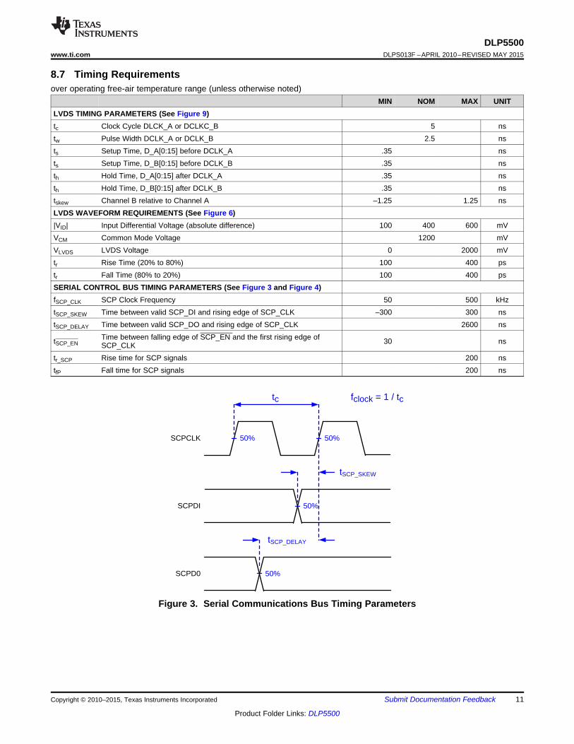
8.7 Timing Requirementsover operating free-air temperature range (unless otherwise noted)
MIN NOM MAX UNITLVDS TIMING PARAMETERS (See Figure 9)tc Clock Cycle DLCK_A or DCLKC_B 5 nstw Pulse Width DCLK_A or DCLK_B 2.5 nsts Setup Time, D_A[0:15] before DCLK_A .35 nsts Setup Time, D_B[0:15] before DCLK_B .35 nsth Hold Time, D_A[0:15] after DCLK_A .35 nsth Hold Time, D_B[0:15] after DCLK_B .35 nstskew Channel B relative to Channel A –1.25 1.25 nsLVDS WAVEFORM REQUIREMENTS (See Figure 6)|VID| Input Differential Voltage (absolute difference) 100 400 600 mVVCM Common Mode Voltage 1200 mVVLVDS LVDS Voltage 0 2000 mVtr Rise Time (20% to 80%) 100 400 pstr Fall Time (80% to 20%) 100 400 psSERIAL CONTROL BUS TIMING PARAMETERS (See Figure 3 and Figure 4)fSCP_CLK SCP Clock Frequency 50 500 kHztSCP_SKEW Time between valid SCP_DI and rising edge of SCP_CLK –300 300 nstSCP_DELAY Time between valid SCP_DO and rising edge of SCP_CLK 2600 ns
Time between falling edge of SCP_EN and the first rising edge oftSCP_EN 30 nsSCP_CLKtr_SCP Rise time for SCP signals 200 nstfP Fall time for SCP signals 200 ns
Figure 3. Serial Communications Bus Timing Parameters
Copyright © 2010–2015, Texas Instruments Incorporated Submit Documentation Feedback 11
Product Folder Links: DLP5500

V /2CC
0 v
SCP_CLK,
SCP_DI,
SCP_EN
Input Controller VCC
tr_SCP
tf_SCP
DLP5500DLPS013F –APRIL 2010–REVISED MAY 2015 www.ti.com
Figure 4. Serial Communications Bus Waveform Requirements
Refer to LVDS Interface section of the Recommended Operating Conditions.Refer to Pin Configuration and Functions for list of LVDS pins.
Figure 5. LVDS Voltage Definitions (References)
12 Submit Documentation Feedback Copyright © 2010–2015, Texas Instruments Incorporated
Product Folder Links: DLP5500

VCM
VLVDS (v)
VID
Tr
(20% - 80%)
Tf
(20% - 80%)
Time
VLVDSmax
VLVDS min
V = V + |½V |IDLVDSmax CM
VLVDS
= VCM
+/- | 1/2 VID
|
VLVDS min = 0
DLP5500www.ti.com DLPS013F –APRIL 2010–REVISED MAY 2015
Not to scale.Refer to LVDS Interface section of the Recommended Operating Conditions.
Figure 6. LVDS Waveform Requirements
Refer to LVDS Interface section of the Recommended Operating Conditions.Refer to Pin Configuration and Functions for list of LVDS pins.
Figure 7. LVDS Equivalent Input Circuit
Copyright © 2010–2015, Texas Instruments Incorporated Submit Documentation Feedback 13
Product Folder Links: DLP5500

SCTRL_ANSCTRL_AP
D_AN(15:0)D_AP(15:0)
D_BN(15:0)D_BP(15:0)
DCLK_BNDCLK_BP
SCTRL_BNSCTRL_BP
DCLK_ANDCLK_AP
Tw Tc
Tw
Th
Th
Ts
Ts
Tske
w
Tw Tc
Tw
Th
Th
Ts
Ts
0.0 * VCC
1.0 * VCC
tftr
1.0 * VID
0.0 * VID
VCM
tftr
LVDS Interface SCP Interface
DLP5500DLPS013F –APRIL 2010–REVISED MAY 2015 www.ti.com
Not to scale.Refer to the Timing Requirements.Refer to Pin Configuration and Functions for list of LVDS pins and SCP pins.
Figure 8. Rise Time and Fall Time
Figure 9. LVDS Timing Waveforms
14 Submit Documentation Feedback Copyright © 2010–2015, Texas Instruments Incorporated
Product Folder Links: DLP5500

DLP5500www.ti.com DLPS013F –APRIL 2010–REVISED MAY 2015
8.8 System Mounting Interface Loads
PARAMETER MIN NOM MAX UNITMaximum system mounting interface Thermal Interface area Static load applied to the 111 Nload to be applied to the: thermal interface area,
See Figure 10Electrical Interface area Static load applied to 55 N
each electrical interfacearea no. 1 and no. 2,See Figure 10
Figure 10. System Interface Loads
Copyright © 2010–2015, Texas Instruments Incorporated Submit Documentation Feedback 15
Product Folder Links: DLP5500

N ± 1
0 1 2
012
M ±
1
DMD Active Array
3
N ± 4
3 M ±
2
M ±
3
M ±
4
N ± 2N ± 3
M x P
N x PM x N Micromirrors
P P
P
Border micromirrors omitted for clarity.
Not to scale.
P
Details omitted for clarity.
DLP5500DLPS013F –APRIL 2010–REVISED MAY 2015 www.ti.com
8.9 Micromirror Array Physical CharacteristicsAdditional details are provided in the Mechanical, Packaging, and Orderable Information section at the end of thisdocument.
PARAMETER VALUE UNITM Number of active micromirror columns 1024
micromirrorsN Number of active micromirror rows 768See MicromirrorP Micromirror pitch Array Physical 10.8 µm
CharacteristicsMicromirror active array width M × P 11.059 mmMicromirror active array height N × P 8.294 mm
Pond ofMicromirror active array border Micromirror 10 micromirrors /side
(POM) (1)
(1) The structure and qualities of the border around the active array includes a band of partially functional micromirrors called the POM.These micromirrors are structurally and/or electrically prevented from tilting toward the bright or ON state, but still require an electricalbias to tilt toward OFF.
Refer to the Micromirror Array Physical Characteristics table for M, N, and P specifications.
Figure 11. Micromirror Array Physical Characteristics
16 Submit Documentation Feedback Copyright © 2010–2015, Texas Instruments Incorporated
Product Folder Links: DLP5500
DLP5500www.ti.com DLPS013F –APRIL 2010–REVISED MAY 2015
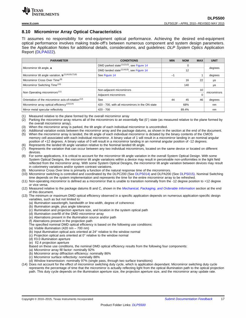
8.10 Micromirror Array Optical CharacteristicsTI assumes no responsibility for end-equipment optical performance. Achieving the desired end-equipmentoptical performance involves making trade-off’s between numerous component and system design parameters.See the Application Notes for additional details, considerations, and guidelines: DLP System Optics ApplicationReport (DLPA022).
PARAMETER CONDITIONS MIN NOM MAX UNIT
DMD parked state (1) (2) (3), see Figure 14 0Micromirror tilt angle, a degrees
DMD landed state (1) (4) (5), see Figure 14 12
Micromirror tilt angle variation, b (1) (4) (6) (7) (8) See Figure 14 –1 1 degrees
Micromirror Cross Over Time (9) 16 22 µs
Micromirror Switching Time (10) 140 µs
Non-adjacent micromirrors 10Non Operating micromirrors (11) micromirrors
Adjacent micromirrors 0
Orientation of the micromirror axis-of-rotation (12) See 44 45 46 degrees
Micromirror array optical efficiency (13) (14) 420 - 700, with all micromirrors in the ON state 68% nm
Mirror metal specular reflectivity 420 - 700 89.4% nm
(1) Measured relative to the plane formed by the overall micromirror array(2) Parking the micromirror array returns all of the micromirrors to an essentially flat (0˚) state (as measured relative to the plane formed by
the overall micromirror array).(3) When the micromirror array is parked, the tilt angle of each individual micromirror is uncontrolled.(4) Additional variation exists between the micromirror array and the package datums, as shown in the section at the end of the document.(5) When the micromirror array is landed, the tilt angle of each individual micromirror is dictated by the binary contents of the CMOS
memory cell associated with each individual micromirror. A binary value of 1 will result in a micromirror landing in an nominal angularposition of +12 degrees. A binary value of 0 will result in a micromirror landing in an nominal angular position of -12 degrees.
(6) Represents the landed tilt angle variation relative to the Nominal landed tilt angle.(7) Represents the variation that can occur between any two individual micromirrors, located on the same device or located on different
devices.(8) For some applications, it is critical to account for the micromirror tilt angle variation in the overall System Optical Design. With some
System Optical Designs, the micromirror tilt angle variations within a device may result in perceivable non-uniformities in the light fieldreflected from the micromirror array. With some System Optical Designs, the micromirror tilt angle variation between devices may resultin colorimetry variations and/or system contrast variations.
(9) Micromirror Cross Over time is primarily a function of the natural response time of the micromirrors.(10) Micromirror switching is controlled and coordinated by the DLPC200 (See DLPS014) and DLPA200 (See DLPS015). Nominal Switching
time depends on the system implementation and represents the time for the entire micromirror array to be refreshed.(11) Non-operating micromirror is defined as a micromirror that is unable to transition nominally from the -12 degree position to +12 degree
or vice versa.(12) Measured relative to the package datums B and C, shown in the Mechanical, Packaging, and Orderable Information section at the end
of this document.(13) The minimum or maximum DMD optical efficiency observed in a specific application depends on numerous application-specific design
variables, such as but not limited to:(a) Illumination wavelength, bandwidth or line-width, degree of coherence(b) Illumination angle, plus angle tolerance(c) Illumination and projection aperture size, and location in the system optical path(d) IIlumination overfill of the DMD micromirror array(e) Aberrations present in the illumination source and/or path(f) Aberrations present in the projection pathThe specified nominal DMD optical efficiency is based on the following use conditions:(a) Visible illumination (420 nm – 700 nm)(b) Input illumination optical axis oriented at 24° relative to the window normal(c) Projection optical axis oriented at 0° relative to the window normal(d) f/3.0 illumination aperture(e) f/2.4 projection apertureBased on these use conditions, the nominal DMD optical efficiency results from the following four components:(a) Micromirror array fill factor: nominally 92%(b) Micromirror array diffraction efficiency: nominally 86%(c) Micromirror surface reflectivity: nominally 88%(d) Window transmission: nominally 97% (single pass, through two surface transitions)
(14) Does not account for the effect of micromirror switching duty cycle, which is application dependant. Micromirror switching duty cyclerepresents the percentage of time that the micromirror is actually reflecting light from the optical illumination path to the optical projectionpath. This duty cycle depends on the illumination aperture size, the projection aperture size, and the micromirror array update rate.
Copyright © 2010–2015, Texas Instruments Incorporated Submit Documentation Feedback 17
Product Folder Links: DLP5500
N ± 1
0 1 2
012
M ±
1
3
N ± 4
3 M ±
2
M ±
3
M ±
4
N ± 2N ± 3
45°
On-StateTilt Direction
Off-StateTilt Direction
Not To Scale
illumination
DLP5500DLPS013F –APRIL 2010–REVISED MAY 2015 www.ti.com
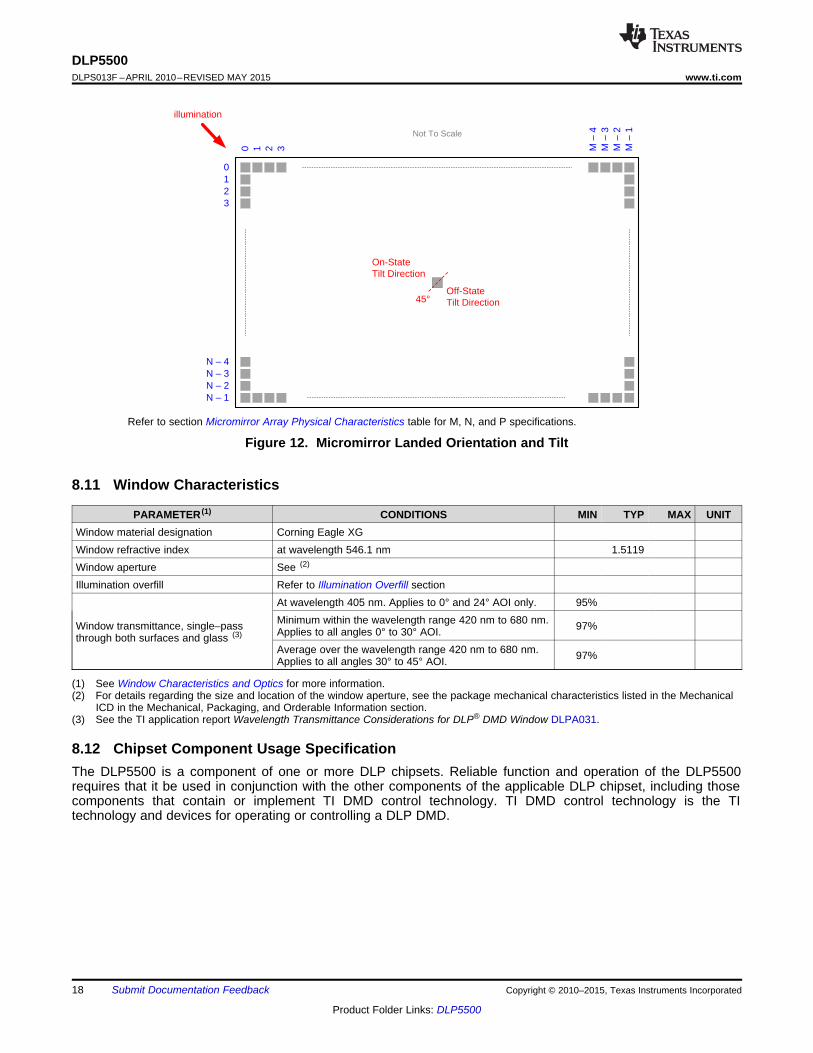
Refer to section Micromirror Array Physical Characteristics table for M, N, and P specifications.
Figure 12. Micromirror Landed Orientation and Tilt
8.11 Window Characteristics
PARAMETER (1) CONDITIONS MIN TYP MAX UNITWindow material designation Corning Eagle XGWindow refractive index at wavelength 546.1 nm 1.5119Window aperture See (2)
Illumination overfill Refer to Illumination Overfill sectionAt wavelength 405 nm. Applies to 0° and 24° AOI only. 95%Minimum within the wavelength range 420 nm to 680 nm.Window transmittance, single–pass 97%Applies to all angles 0° to 30° AOI.through both surfaces and glass (3)
Average over the wavelength range 420 nm to 680 nm. 97%Applies to all angles 30° to 45° AOI.
(1) See Window Characteristics and Optics for more information.(2) For details regarding the size and location of the window aperture, see the package mechanical characteristics listed in the Mechanical
ICD in the Mechanical, Packaging, and Orderable Information section.(3) See the TI application report Wavelength Transmittance Considerations for DLP® DMD Window DLPA031.
8.12 Chipset Component Usage SpecificationThe DLP5500 is a component of one or more DLP chipsets. Reliable function and operation of the DLP5500requires that it be used in conjunction with the other components of the applicable DLP chipset, including thosecomponents that contain or implement TI DMD control technology. TI DMD control technology is the TItechnology and devices for operating or controlling a DLP DMD.
18 Submit Documentation Feedback Copyright © 2010–2015, Texas Instruments Incorporated
Product Folder Links: DLP5500

DLP5500www.ti.com DLPS013F –APRIL 2010–REVISED MAY 2015
9 Detailed Description
9.1 OverviewDLP5500 is a 0.55 inch diagonal spatial light modulator which consists of an array of highly reflective aluminummicromirrors. Pixel array size and square grid pixel arrangement are shown in Figure 11.
The DMD is an electrical input, optical output micro-electrical-mechanical system (MEMS). The electricalinterface is Low Voltage Differential Signaling (LVDS), Double Data Rate (DDR).
DLP5500 DMD consists of a two-dimensional array of 1-bit CMOS memory cells. The array is organized in a gridof M memory cell columns by N memory cell rows. Refer to the Functional Block Diagram.
The positive or negative deflection angle of the micromirrors can be individually controlled by changing theaddress voltage of underlying CMOS addressing circuitry and micromirror reset signals (MBRST).
Each cell of the M × N memory array drives its true and complement (‘Q’ and ‘QB’) data to two electrodesunderlying one micromirror, one electrode on each side of the diagonal axis of rotation. Refer to Figure 14. Themicromirrors are electrically tied to the micromirror reset signals (MBRST) and the micromirror array is dividedinto reset groups.
Electrostatic potentials between a micromirror and its memory data electrodes cause the micromirror to tilttoward the illumination source in a DLP projection system or away from it, thus reflecting its incident light into orout of an optical collection aperture. The positive (+) tilt angle state corresponds to an 'on' pixel, and the negative(–) tilt angle state corresponds to an 'off' pixel.
Refer to Micromirror Array Optical Characteristics for the ± tilt angle specifications. Refer to the Pin Configurationand Functions for more information on micromirror clocking pulse (reset) control.
Copyright © 2010–2015, Texas Instruments Incorporated Submit Documentation Feedback 19
Product Folder Links: DLP5500

DLP5500DLPS013F –APRIL 2010–REVISED MAY 2015 www.ti.com
9.2 Functional Block Diagram
20 Submit Documentation Feedback Copyright © 2010–2015, Texas Instruments Incorporated
Product Folder Links: DLP5500

DLP5500www.ti.com DLPS013F –APRIL 2010–REVISED MAY 2015
9.3 Feature DescriptionThe DLP5500 device consists of 786,432 highly reflective, digitally switchable, micrometer-sized mirrors(micromirrors) organized in a two-dimensional orthogonal pixel array. Refer to Figure 11 and Figure 13.
Each aluminum micromirror is switchable between two discrete angular positions, –a and +a. The angularpositions are measured relative to the micromirror array plane, which is parallel to the silicon substrate. Refer toMicromirror Array Optical Characteristics and Figure 14.
The parked position of the micromirror is not a latched position and is therefore not necessarily perfectly parallelto the array plane. Individual micromirror flat state angular positions may vary. Tilt direction of the micromirror isperpendicular to the hinge-axis. The on-state landed position is directed toward the left-top edge of the package,as shown in Figure 13.
Each individual micromirror is positioned over a corresponding CMOS memory cell. The angular position of aspecific micromirror is determined by the binary state (logic 0 or 1) of the corresponding CMOS memory cellcontents, after the mirror clocking pulse is applied. The angular position (–a and +a) of the individualmicromirrors changes synchronously with a micromirror clocking pulse, rather than being coincident with theCMOS memory cell data update.
Writing logic 1 into a memory cell followed by a mirror clocking pulse results in the corresponding micromirrorswitching to the +a position. Writing logic 0 into a memory cell followed by a mirror clocking pulse results in thecorresponding micromirror switching to the – a position.
Updating the angular position of the micromirror array consists of two steps. First, update the contents of theCMOS memory. Second, apply a micromirror clocking pulse (reset) to all or a portion of the micromirror array(depending upon the configuration of the system). Micromirror reset pulses are generated externally by theDLPC200 controller in conjunction with the DLPA200 analog driver, with application of the pulses beingcoordinated by the DLPC200 controller.
For more information, see the TI application report DLPA008, DMD101: Introduction to Digital Micromirror Device(DMD) Technology.
Copyright © 2010–2015, Texas Instruments Incorporated Submit Documentation Feedback 21
Product Folder Links: DLP5500

DMDMicromirror
Array
0
N±1
0 M±
1
Active Micromirror Array
(Border micromirrors eliminated for clarity)
P (um)
Micromirror Pitch Micromirror Hinge-Axis Orientation
³2Q-6WDWH´Tilt Direction
³2II-6WDWH´Tilt Direction
45°
P (um)
P (
um)P (
um)
Incident Illumination
Package Pin A1 Corner
Details Omitted For Clarity.
Not To Scale.
DLP5500DLPS013F –APRIL 2010–REVISED MAY 2015 www.ti.com
Feature Description (continued)
Refer to Figure 11 and Figure 12.
Figure 13. Micromirror Array, Pitch, Hinge Axis Orientation22 Submit Documentation Feedback Copyright © 2010–2015, Texas Instruments Incorporated
Product Folder Links: DLP5500

DMD
For Reference
Flat-State( ³SDUNHG´�)
Micromirror Position
³2II-6WDWH´Micromirror
³2Q-6WDWH´Micromirror
Silicon SubstrateSilicon Substrate
a ± b -a ± b
Two³2Q-6WDWH´
Micromirrors
Two³2II-6WDWH´
MicromirrorsIncident
Illumination-Light P
ath
Incident
Illumination-Light P
athPro
ject
ed-L
ight
Pat
h
Off-Stat
e-Lig
ht
Path
Package Pin A1 Corner
Details Omitted For Clarity.
Not To Scale.
Incident Illumination
Incident
Illumination-Light Path
DLP5500www.ti.com DLPS013F –APRIL 2010–REVISED MAY 2015
Feature Description (continued)
Micromirror States: On, Off, Flat
Figure 14. Micromirror States: On, Off, Flat
Copyright © 2010–2015, Texas Instruments Incorporated Submit Documentation Feedback 23
Product Folder Links: DLP5500
DLP5500DLPS013F –APRIL 2010–REVISED MAY 2015 www.ti.com
9.4 Device Functional ModesDMD functional modes are controlled by the DLPC200 digital display controller. See the DLPC200 data sheetlisted in Related Documentation. Contact a TI applications engineer for more information.
The DLPC200 provides two basic functional mode types to control the DLP5500 DMD: video and structured light.
9.4.1 Video ModesThe controller accepts RGB-8-8-8 input to port 1 or port 2 through a selectable MUX. XGA video information isdisplayed on the DMD at 6 to 60 fps.
An internal pattern generator can generate RGB-8-8-8 video patterns into an internal selectable MUX forverification and debug purposes.
9.4.2 Structured Light ModesThe DLPC200 provides two structured light modes: static image buffer and real-time structured light.
9.4.2.1 Static Image Buffer ModeImage data can be loaded into parallel flash memory to load to DDR2 memory at startup to be displayed, or canbe loaded over USB or the SPI port directly to DDR2 memory to be displayed. Binary (1-bit) or grayscale (8-bit)patterns can be displayed. The memory will hold 960 binary patterns or 120 grayscale patterns.
Binary (1-bit) patterns can be displayed at up to 5000 binary patterns per second. These patterns assume aconstant illumination and do not depend on illumination modulation
Grayscale (8-bit) patterns assume illumination modulation in order to achieve higher pattern rates. When thepattern rate requires that the lower significant bit(s) be shorter than the rate that the DMD can be switched, thesebits will require the source to be modulated to achieve the shorter time required. The trade-off is dark time duringthese bits. At the maximum 500 Hz grayscale pattern rate, the dark time approaches 75%.
9.4.2.2 Real Time Structured Light ModeRGB-8-8-8 60 fps data can be input into port 1 or port 2 and reinterpreted as up to 24 binary (1-bit) patterns orthree grayscale (8-bit) patterns. The specified number of patterns is displayed equally during the exposure timespecified. Any unused RGB-8-8-8 data in the video frame must be filled with data, usually 0s.
For example, during one video frame (16.67 ms), 12 binary patterns of the 24 RGB bits are requested to bedisplayed during half of the video frame time (exposure time = 8.33 ms). Each of the eight red bits and the fourmost significant green bits are displayed as a binary pattern for 694 µs each. The remaining bits are ignored andthe remaining 8.33 ms of the frame will be dark.
9.5 Window Characteristics and Optics
NOTETI assumes no responsibility for image quality artifacts or DMD failures caused by opticalsystem operating conditions exceeding limits described previously.
9.5.1 Optical Interface and System Image QualityTI assumes no responsibility for end-equipment optical performance. Achieving the desired end-equipmentoptical performance involves making trade-offs between numerous component and system design parameters.Optimizing system optical performance and image quality strongly relate to optical system design parametertrades. Although it is not possible to anticipate every conceivable application, projector image quality and opticalperformance is contingent on compliance to the optical system operating conditions described in the followingsections.
24 Submit Documentation Feedback Copyright © 2010–2015, Texas Instruments Incorporated
Product Folder Links: DLP5500

DLP5500www.ti.com DLPS013F –APRIL 2010–REVISED MAY 2015
Window Characteristics and Optics (continued)9.5.2 Numerical Aperture and Stray Light ControlThe angle defined by the numerical aperture of the illumination and projection optics at the DMD optical areashould be the same. This angle should not exceed the nominal device mirror tilt angle unless appropriateapertures are added in the illumination and/or projection pupils to block out flat-state and stray light from theprojection lens. The mirror tilt angle defines DMD capability to separate the "ON" optical path from any other lightpath, including undesirable flat-state specular reflections from the DMD window, DMD border structures, or othersystem surfaces near the DMD such as prism or lens surfaces. If the numerical aperture exceeds the mirror tiltangle, or if the projection numerical aperture angle is more than two degrees larger than the illuminationnumerical aperture angle, objectionable artifacts in the display’s border and/or active area could occur.
9.5.3 Pupil MatchTI’s optical and image quality specifications assume that the exit pupil of the illumination optics is nominallycentered within 2° (two degrees) of the entrance pupil of the projection optics. Misalignment of pupils can createobjectionable artifacts in the display’s border and/or active area, which may require additional system aperturesto control, especially if the numerical aperture of the system exceeds the pixel tilt angle.
9.5.4 Illumination OverfillThe active area of the device is surrounded by an aperture on the inside DMD window surface that masksstructures of the DMD device assembly from normal view. The aperture is sized to anticipate several opticaloperating conditions. Overfill light illuminating the window aperture can create artifacts from the edge of thewindow aperture opening and other surface anomalies that may be visible on the screen. The illumination opticalsystem should be designed to limit light flux incident anywhere on the window aperture from exceedingapproximately 10% of the average flux level in the active area. Depending on the particular system’s opticalarchitecture, overfill light may have to be further reduced below the suggested 10% level in order to beacceptable.
9.6 Micromirror Array Temperature CalculationAchieving optimal DMD performance requires proper management of the maximum DMD case temperature, themaximum temperature of any individual micromirror in the active array, the maximum temperature of the windowaperture, and the temperature gradient between case temperature and the predicted micromirror arraytemperature. (see Figure 15).
Refer to the Recommended Operating Conditions for applicable temperature limits.
9.6.1 Package Thermal ResistanceThe DMD is designed to conduct absorbed and dissipated heat to the back of the Series 450 package where itcan be removed by an appropriate heat sink. The heat sink and cooling system must be capable of maintainingthe package within the specified operational temperatures, refer to Figure 15. The total heat load on the DMD istypically driven by the incident light absorbed by the active area; although other contributions include light energyabsorbed by the window aperture and electrical power dissipation of the array.
9.6.2 Case TemperatureThe temperature of the DMD case can be measured directly. For consistency, Thermal Test Point locations TP1- TP5 are defined, as shown in Figure 15.
Copyright © 2010–2015, Texas Instruments Incorporated Submit Documentation Feedback 25
Product Folder Links: DLP5500

DLP5500DLPS013F –APRIL 2010–REVISED MAY 2015 www.ti.com
Micromirror Array Temperature Calculation (continued)
Figure 15. Thermal Test Point Location
9.6.3 Micromirror Array Temperature Calculation for Uniform IlluminationMicromirror array temperature cannot be measured directly; therefore it must be computed analytically frommeasurement points (Figure 15), the package thermal resistance, the electrical power, and the illumination heatload. The relationship between micromirror array temperature and the case temperature are provided byEquation 1 and Equation 2:
TArray = TCeramic + (QArray x RArray-To-Ceramic) (1)QArray = QELE + QILL
Where the following elements are defined as:• TArray = computed micromirror array temperature (°C)• TCeramic = Ceramic temperature (°C) (TC2 Location Figure 15)• QArray = Total DMD array power (electrical + absorbed) (measured in Watts)• RArray-To-Ceramic = thermal resistance of DMD package from array to TC2 (°C/Watt) (see Package Thermal
Resistance)• QELE = Nominal electrical power (Watts)• QILL = Absorbed illumination energy (Watts) (2)
An example calculation is provided below based on a traditional DLP Video projection system. The electricalpower dissipation of the DMD is variable and depends on the voltages, data rates, and operating frequencies.The nominal electrical power dissipation to be used in the calculation is 2.0 Watts. Thus, QELE = 2.0 Watts. Theabsorbed power from the illumination source is variable and depends on the operating state of the mirrors andthe intensity of the light source. It's based on modeling and measured data from DLP projection system.
QILL = CL2W x SL
Where:• CL2W is a Lumens to Watts constant, and can be estimated at 0.00274 Watt/Lumen• SL = Screen Lumens nominally measured to be 2000 lumens• Qarray = 2.0 + (0.00274 x 2000) = 7.48 watts, Estimated total power on micromirror Array• TCeramic = 55°C, assumed system measurement• TArray(micromirror active array temperature) = 55°C + (7.48 watts x 0.6 °C/watt) = 59.5°C (3)
26 Submit Documentation Feedback Copyright © 2010–2015, Texas Instruments Incorporated
Product Folder Links: DLP5500

DLP5500www.ti.com DLPS013F –APRIL 2010–REVISED MAY 2015
Micromirror Array Temperature Calculation (continued)For additional explanation of DMD Mechanical and Thermal calculations and considerations please refer to DLPSeries-450 DMD and System Mounting Concepts (DLPA015).
9.7 Micromirror Landed-on/Landed-Off Duty Cycle
9.7.1 Definition of Micromirror Landed-On/Landed-Off Duty CycleThe micromirror landed-on/landed-off duty cycle (landed duty cycle) denotes the amount of time (as apercentage) that an individual micromirror is landed in the On–state versus the amount of time the samemicromirror is landed in the Off–state.
As an example, a landed duty cycle of 100/0 indicates that the referenced pixel is in the On-state 100% of thetime (and in the Off-state 0% of the time); whereas 0/100 would indicate that the pixel is in the Off-state 100% ofthe time. Likewise, 50/50 indicates that the pixel is On 50% of the time and Off 50% of the time.
Note that when assessing landed duty cycle, the time spent switching from one state (ON or OFF) to the otherstate (OFF or ON) is considered negligible and is thus ignored.
Since a micromirror can only be landed in one state or the other (On or Off), the two numbers (percentages)always add to 100.
9.7.2 Landed Duty Cycle and Useful Life of the DMDKnowing the long-term average landed duty cycle (of the end product or application) is important becausesubjecting all (or a portion) of the DMD’s micromirror array (also called the active array) to an asymmetric landedduty cycle for a prolonged period of time can reduce the DMD’s usable life.
Note that it is the symmetry/asymmetry of the landed duty cycle that is of relevance. The symmetry of the landedduty cycle is determined by how close the two numbers (percentages) are to being equal. For example, a landedduty cycle of 50/50 is perfectly symmetrical whereas a landed duty cycle of 100/0 or 0/100 is perfectlyasymmetrical.
9.7.3 Landed Duty Cycle and Operational DMD TemperatureOperational DMD Temperature and Landed Duty Cycle interact to affect the DMD’s usable life, and thisinteraction can be exploited to reduce the impact that an asymmetrical Landed Duty Cycle has on the DMD’susable life. This is quantified in the de-rating curve shown in Figure 1. The importance of this curve is that:• All points along this curve represent the same usable life.• All points above this curve represent lower usable life (and the further away from the curve, the lower the
usable life).• All points below this curve represent higher usable life (and the further away from the curve, the higher the
usable life).
In practice, this curve specifies the Maximum Operating DMD Temperature that the DMD should be operated atfor a give long-term average Landed Duty Cycle.
9.7.4 Estimating the Long-Term Average Landed Duty Cycle of a Product or ApplicationDuring a given period of time, the Landed Duty Cycle of a given pixel follows from the image content beingdisplayed by that pixel.
For example, in the simplest case, when displaying pure-white on a given pixel for a given time period, that pixelwill experience a 100/0 Landed Duty Cycle during that time period. Likewise, when displaying pure-black, thepixel will experience a 0/100 Landed Duty Cycle.
Between the two extremes (ignoring for the moment color and any image processing that may be applied to anincoming image), the Landed Duty Cycle tracks one-to-one with the gray scale value, as shown in Table 1.
Copyright © 2010–2015, Texas Instruments Incorporated Submit Documentation Feedback 27
Product Folder Links: DLP5500

DLP5500DLPS013F –APRIL 2010–REVISED MAY 2015 www.ti.com
Table 1. Grayscale Value and Landed Duty CycleGRAYSCALE VALUE LANDED DUTY CYCLE
0% 0/10010% 10/9020% 20/8030% 30/7040% 40/6050% 50/5060% 60/4070% 70/3080% 80/2090% 90/10100% 100/0
Accounting for color rendition (but still ignoring image processing) requires knowing both the color intensity (from0% to 100%) for each constituent primary color (red, green, and/or blue) for the given pixel as well as the colorcycle time for each primary color, where “color cycle time” is the total percentage of the frame time that a givenprimary must be displayed in order to achieve the desired white point.
During a given period of time, the landed duty cycle of a given pixel can be calculated as follows:Landed Duty Cycle = (Red_Cycle_% × Red_Scale_Value) + (Green_Cycle_% × Green_Scale_Value) + (Blue_Cycle_%× Blue_Scale_Value)
where• Red_Cycle_%, Green_Cycle_%, and Blue_Cycle_%, represent the percentage of the frame time that Red,
Green, and Blue are displayed (respectively) to achieve the desired white point. (4)
For example, assume that the red, green and blue color cycle times are 50%, 20%, and 30% respectively (inorder to achieve the desired white point), then the Landed Duty Cycle for various combinations of red, green,blue color intensities would be as shown in Table 2.
Table 2. Example Landed Duty Cycle for Full-ColorRed Cycle Percentage Green Cycle Percentage Blue Cycle Percentage
50% 20% 30% Landed Duty CycleRed Scale Value Green Scale Value Blue Scale Value
0% 0% 0% 0/100100% 0% 0% 50/50
0% 100% 0% 20/800% 0% 100% 30/70
12% 0% 0% 6/940% 35% 0% 7/930% 0% 60% 18/82
100% 100% 0% 70/300% 100% 100% 50/50
100% 0% 100% 80/2012% 35% 0% 13/870% 35% 60% 25/75
12% 0% 60% 24/76100% 100% 100% 100/0
28 Submit Documentation Feedback Copyright © 2010–2015, Texas Instruments Incorporated
Product Folder Links: DLP5500

DLP5500www.ti.com DLPS013F –APRIL 2010–REVISED MAY 2015
10 Application and Implementation
NOTEInformation in the following applications sections is not part of the TI componentspecification, and TI does not warrant its accuracy or completeness. TI’s customers areresponsible for determining suitability of components for their purposes. Customers shouldvalidate and test their design implementation to confirm system functionality.
10.1 Application InformationThe DLP5500 (0.55-inch XGA DMD) is controlled by the DLPC200 contoller in conjunction with the DLPA200driver. This combination can be used for a number of applications from 3D printers to microscopes.
The most common application is for 3D structured light measurement applications. In this application, patterns(binary, grayscale, or even full color) are projected onto the target and the distortion of the patterns are recordedby an imaging device to extract 3D (x, y, z) surface information.
Copyright © 2010–2015, Texas Instruments Incorporated Submit Documentation Feedback 29
Product Folder Links: DLP5500

Exp
an
sio
nP
ort
Co
nn
ec
tor
DLPA200 Control Interface
Micromirror
Resets
Micromirror Data Interface
Micromirror Control Interface
RED ENABLE
GREEN ENABLE
BLUE ENABLE
INFRARED ENABLE
LED Lit Status
LED SPI Interface
Port 2 DATA( 23:0 )
Port 2 VSYNC
Port 2 HSYNC
Port 2 Data Valid
Port 2 Clock
Port 1 DATA( 23:0 )
Port 1 VSYNC
Port 1 HSYNC
Port 1 Data Valid
Port 1 Clock
I2C Interface
Port
1 Inte
rface
Port
2In
terf
ace
DM
DIn
terf
ace
Illu
min
ation
Inte
rface
DLP
A200
Inte
rface
SYNC OUT 1
SYNC OUT 2
SYNC OUT 3User
SY
NC
Inte
rface
Illumination
OpticsProjection
Optics
Configuration Interface
RESET
SRAM_CE
FLASH_SRAM_OE
FLASH_SRAM_WE
FLASH_SRAM_RST
FLASH_CE
SRAM_LB, SRAM_UB
USB Interface
SD
RA
MIn
terf
ace
User
Fla
sh
/S
RA
MIn
terf
ace
Port 2 SPI Interface
HDMI
DLPR200USB PROM
DLPR200USB
DLPR200F PROM
DLPR200F
DLP5500DLPS013F –APRIL 2010–REVISED MAY 2015 www.ti.com
10.2 Typical ApplicationA schematic is shown in Figure 16 for projecting RGB and IR structured light patterns onto a measurementtarget. Typically, an imaging device is triggered through one of the three syncs to record the data as each patternis displayed.
Figure 16. Typical RGB + IR Structured Light Application
30 Submit Documentation Feedback Copyright © 2010–2015, Texas Instruments Incorporated
Product Folder Links: DLP5500

DLP5500www.ti.com DLPS013F –APRIL 2010–REVISED MAY 2015
Typical Application (continued)10.2.1 Design RequirementsAll applications using the DLP 0.55-inch XGA chipset require the DLPC200 controller, the DLPA200 driver, andthe DLP5500 DMD for correct operation. The system also requires user supplied SRAM and a configurationPROM programmed with the DLPR200F program file and a 50-MHz oscillator is for operation. For further details,refer to the DLPC200 controller data sheet (DLPS014) and the DLPA200 analog driver data sheet (DLPS015).
10.2.2 Detailed Design Procedure
10.2.2.1 DLP5500 System InterfaceImages are displayed on the DLP5500 via the DLPC200 controller and the DLPA200 driver. The DLP5500interface consists of a 200-MHz (nominal) half-bus DDR input-only interface with LVDS signaling. The serialcommunications port (SCP), 125-kHz nominal, is used by the DLPC200 to read or write control data to both theDLP5500 and the DLPA200. The following listed signals support data transfer to the DLP5500 and DLPA200.
• DMD, 200 MHz– DMD_CLK_AP, DMD_CLK_AN – DMD clock for A– DMD_CLK_BP, DMD_CLK_BN – DMD clock for B– DMD_DAT_AP, DMD_DAT_AN(1, 3, 5, 7, 9, 11, 13, 15) – Data bus A (odd-numbered pins are used for
half-bus)– DMD_DAT_BP, DMD_DAT_BN(1, 3, 5, 7, 9, 11, 13, 15) – Data bus B (odd-numbered pins are used for
half-bus)– DMD_SCRTL_AP, DMD_SCRTL_AN – S-control for A– DMD_SCRTL_BP, DMD_SCRTL_BN – S-control for B
• DLPA200, 125 kHz– SCP_DMD_RST_CLK – SCP clock– SCP_DMD_EN – Enable DMD communication– SCP_RST_EN – Enable DLPA200 communication– SCP_DMD_RST_DI – Input data– SCP_DMD_RST_DO – Output data
Copyright © 2010–2015, Texas Instruments Incorporated Submit Documentation Feedback 31
Product Folder Links: DLP5500

DLP5500DLPS013F –APRIL 2010–REVISED MAY 2015 www.ti.com
11 Power Supply Recommendations
11.1 DMD Power-Up and Power-Down ProceduresThe DLP5500 power-up and power-down procedures are defined by the DLPC200 data sheet (DLPS012) andthe 0.55 XGA Chipset data sheet (DLPZ004). These procedures must be followed to ensure reliable operation ofthe device.
CAUTIONFailure to adhere to the prescribed power-up and power-down procedures may affectdevice reliability.
12 Layout
12.1 Layout GuidelinesThe DLP5500 is part of a chipset that is controlled by the DLPC200 in conjunction with the DLPA200. Theseguidelines are targeted at designing a PCB board with these components.
12.1.1 Impedance RequirementsSignals should be routed to have a matched impedance of 50 Ω ±10% except for LVDS differential pairs(DMD_DAT_Xnn, DMD_DCKL_Xn, and DMD_SCTRL_Xn) and DDR2 differential clock pairs (MEM_CLK_nn),which should be matched to 100 Ω ±10% across each pair.
12.1.2 PCB Signal RoutingWhen designing a PCB board for the DLP5500 controlled by the DLPC200 in conjunction with the DLPA200, thefollowing are recommended:
Signal trace corners should be no sharper than 45°. Adjacent signal layers should have the predominate tracesrouted orthogonal to each other. TI recommends that critical signals be hand routed in the following order: DDR2Memory, DMD (LVDS signals), then DLPA200 signals.
TI does not recommend signal routing on power or ground planes.
TI does not recommend ground plane slots.
High speed signal traces should not cross over slots in adjacent power and/or ground planes.
Table 3. LVDS Trace ConstraintsSignal Constraints
P-to-N data, clock, and SCTRL: <10 mils (0.25 mm); Pair-to-pair <10 mils (0.25 mm); Bundle-to-bundle<2000 mils (50 mm, for example DMD_DAT_Ann to DMD_DAT_Bnn).
LVDS (DMD_DAT_xnn, All matching should include internal trace lengths. See Pin Configuration and Functions for internalDMD_DCKL_xn, and package trace lengths.
DMD_SCTRL_xn) Trace width: 4 mil (0.1 mm)Trace spacing: In ball field – 4 mil (0.11 mm); PCB etch – 14 mil (0.36 mm)Maximum recommended trace length <6 inches (150 mm)
Table 4. Power and Mirror Clocking Pulse Trace Widths and SpacingMinimum Trace Minimum TraceSignal Name Layout RequirementsWidth Spacing
GND Maximize 5 mil (0.13 mm) Maximize trace width to connecting pin as a minimumVCC, VCC2 20 mil (0.51 mm) 10 mil (0.25 mm)
MBRST[15:0] 10 mil (0.25 mm) 10 mil (0.25 mm)
32 Submit Documentation Feedback Copyright © 2010–2015, Texas Instruments Incorporated
Product Folder Links: DLP5500

DLP5500www.ti.com DLPS013F –APRIL 2010–REVISED MAY 2015
12.1.3 FiducialsFiducials for automatic component insertion should be 0.05-inch copper with a 0.1-inch cutout (antipad). Fiducialsfor optical auto insertion are placed on three corners of both sides of the PCB.
12.2 Layout ExampleFor LVDS (and other differential signal) pairs and groups, it is important to match trace lengths. In the area of thedashed lines, Figure 17 shows correct matching of signal pair lengths with serpentine sections to maintain thecorrect impedance.
Figure 17. Mitering LVDS Traces to Match Lengths
Copyright © 2010–2015, Texas Instruments Incorporated Submit Documentation Feedback 33
Product Folder Links: DLP5500

TI Internal Numbering
Part 2 of Serial Number(7 characters)
Part 1 of Serial Number(7 characters)
GH
XX
XX
X L
LLLLLM
*1076X
XX
XX
X
YY
YY
YY
Y
2-Dimensional Matrix Code(DLP5500 Device Descriptor
and Serial No.)
DLP5500Device Descriptor
DLP5500DLPS013F –APRIL 2010–REVISED MAY 2015 www.ti.com
13 Device and Documentation Support
13.1 Device Support
13.1.1 Device NomenclatureThe device marking consists of the fields shown in Figure 18.
Figure 18. DMD Marking (Device Top View)
13.2 Documentation Support
13.2.1 Related DocumentationThe following documents contain additional information related to the use of the DLP5500 device:• DLP 0.55 XGA Chip-Set data sheet DLPZ004• DLPC200 Digital Controller data sheet DLPS014• DLPA200 DMD Analog Reset Driver DLPS015• DLP Series-450 DMD and System Mounting Concepts DLPA015• DLPC200 API Reference Manual DLPA024• DLPC200 API Programmer's Guide DLPA014• s4xx DMD Cleaning Application Note DLPA025• s4xx DMD Handling Application Note DLPA019
13.3 Related DocumentationThe table below lists quick access links. Categories include technical documents, support and communityresources, tools and software, and quick access to sample or buy.
Related LinksTECHNICAL TOOLS & SUPPORT &PARTS PRODUCT FOLDER SAMPLE & BUY DOCUMENTS SOFTWARE COMMUNITY
DLPA200 Click here Click here Click here Click here Click hereDLPC200 Click here Click here Click here Click here Click here
13.4 Community ResourcesThe following links connect to TI community resources. Linked contents are provided "AS IS" by the respectivecontributors. They do not constitute TI specifications and do not necessarily reflect TI's views; see TI's Terms ofUse.
34 Submit Documentation Feedback Copyright © 2010–2015, Texas Instruments Incorporated
Product Folder Links: DLP5500

DLP5500www.ti.com DLPS013F –APRIL 2010–REVISED MAY 2015
Community Resources (continued)TI E2E™ Online Community TI's Engineer-to-Engineer (E2E) Community. Created to foster collaboration
among engineers. At e2e.ti.com, you can ask questions, share knowledge, explore ideas and helpsolve problems with fellow engineers.
Design Support TI's Design Support Quickly find helpful E2E forums along with design support tools andcontact information for technical support.
13.5 TrademarksE2E is a trademark of Texas Instruments.DLP is a registered trademark of Texas Instruments.All other trademarks are the property of their respective owners.
13.6 Electrostatic Discharge CautionThese devices have limited built-in ESD protection. The leads should be shorted together or the device placed in conductive foamduring storage or handling to prevent electrostatic damage to the MOS gates.
13.7 GlossarySLYZ022 — TI Glossary.
This glossary lists and explains terms, acronyms, and definitions.
14 Mechanical, Packaging, and Orderable InformationThe following pages include mechanical, packaging, and orderable information. This information is the mostcurrent data available for the designated devices. This data is subject to change without notice and revision ofthis document. For browser-based versions of this data sheet, refer to the left-hand navigation.
Copyright © 2010–2015, Texas Instruments Incorporated Submit Documentation Feedback 35
Product Folder Links: DLP5500


PACKAGE OPTION ADDENDUM
www.ti.com 5-Apr-2018
Addendum-Page 1
PACKAGING INFORMATION
Orderable Device Status(1)
Package Type PackageDrawing
Pins PackageQty
Eco Plan(2)
Lead/Ball Finish(6)
MSL Peak Temp(3)
Op Temp (°C) Device Marking(4/5)
Samples
DLP5500BFYA ACTIVE CPGA FYA 149 5 RoHS & Green(In Work)
NI-PD-AU Level-1-NC-NC
DLPA200PFP ACTIVE HTQFP PFP 80 5 Pb-Free(RoHS)
CU NIPDAU Level-2-260C-1 YEAR
DLPC200ZEW ACTIVE BGA ZEW 780 5 Green (RoHS& no Sb/Br)
Call TI Level-3-260C-168 HR
(1) The marketing status values are defined as follows:ACTIVE: Product device recommended for new designs.LIFEBUY: TI has announced that the device will be discontinued, and a lifetime-buy period is in effect.NRND: Not recommended for new designs. Device is in production to support existing customers, but TI does not recommend using this part in a new design.PREVIEW: Device has been announced but is not in production. Samples may or may not be available.OBSOLETE: TI has discontinued the production of the device.
(2) RoHS: TI defines "RoHS" to mean semiconductor products that are compliant with the current EU RoHS requirements for all 10 RoHS substances, including the requirement that RoHS substancedo not exceed 0.1% by weight in homogeneous materials. Where designed to be soldered at high temperatures, "RoHS" products are suitable for use in specified lead-free processes. TI mayreference these types of products as "Pb-Free".RoHS Exempt: TI defines "RoHS Exempt" to mean products that contain lead but are compliant with EU RoHS pursuant to a specific EU RoHS exemption.Green: TI defines "Green" to mean the content of Chlorine (Cl) and Bromine (Br) based flame retardants meet JS709B low halogen requirements of <=1000ppm threshold. Antimony trioxide basedflame retardants must also meet the <=1000ppm threshold requirement.
(3) MSL, Peak Temp. - The Moisture Sensitivity Level rating according to the JEDEC industry standard classifications, and peak solder temperature.
(4) There may be additional marking, which relates to the logo, the lot trace code information, or the environmental category on the device.
(5) Multiple Device Markings will be inside parentheses. Only one Device Marking contained in parentheses and separated by a "~" will appear on a device. If a line is indented then it is a continuationof the previous line and the two combined represent the entire Device Marking for that device.
(6) Lead/Ball Finish - Orderable Devices may have multiple material finish options. Finish options are separated by a vertical ruled line. Lead/Ball Finish values may wrap to two lines if the finishvalue exceeds the maximum column width.
Important Information and Disclaimer:The information provided on this page represents TI's knowledge and belief as of the date that it is provided. TI bases its knowledge and belief on informationprovided by third parties, and makes no representation or warranty as to the accuracy of such information. Efforts are underway to better integrate information from third parties. TI has taken andcontinues to take reasonable steps to provide representative and accurate information but may not have conducted destructive testing or chemical analysis on incoming materials and chemicals.TI and TI suppliers consider certain information to be proprietary, and thus CAS numbers and other limited information may not be available for release.

PACKAGE OPTION ADDENDUM
www.ti.com 5-Apr-2018
Addendum-Page 2
In no event shall TI's liability arising out of such information exceed the total purchase price of the TI part(s) at issue in this document sold by TI to Customer on an annual basis.

IMPORTANT NOTICE
Texas Instruments Incorporated (TI) reserves the right to make corrections, enhancements, improvements and other changes to itssemiconductor products and services per JESD46, latest issue, and to discontinue any product or service per JESD48, latest issue. Buyersshould obtain the latest relevant information before placing orders and should verify that such information is current and complete.TI’s published terms of sale for semiconductor products (http://www.ti.com/sc/docs/stdterms.htm) apply to the sale of packaged integratedcircuit products that TI has qualified and released to market. Additional terms may apply to the use or sale of other types of TI products andservices.Reproduction of significant portions of TI information in TI data sheets is permissible only if reproduction is without alteration and isaccompanied by all associated warranties, conditions, limitations, and notices. TI is not responsible or liable for such reproduceddocumentation. Information of third parties may be subject to additional restrictions. Resale of TI products or services with statementsdifferent from or beyond the parameters stated by TI for that product or service voids all express and any implied warranties for theassociated TI product or service and is an unfair and deceptive business practice. TI is not responsible or liable for any such statements.Buyers and others who are developing systems that incorporate TI products (collectively, “Designers”) understand and agree that Designersremain responsible for using their independent analysis, evaluation and judgment in designing their applications and that Designers havefull and exclusive responsibility to assure the safety of Designers' applications and compliance of their applications (and of all TI productsused in or for Designers’ applications) with all applicable regulations, laws and other applicable requirements. Designer represents that, withrespect to their applications, Designer has all the necessary expertise to create and implement safeguards that (1) anticipate dangerousconsequences of failures, (2) monitor failures and their consequences, and (3) lessen the likelihood of failures that might cause harm andtake appropriate actions. Designer agrees that prior to using or distributing any applications that include TI products, Designer willthoroughly test such applications and the functionality of such TI products as used in such applications.TI’s provision of technical, application or other design advice, quality characterization, reliability data or other services or information,including, but not limited to, reference designs and materials relating to evaluation modules, (collectively, “TI Resources”) are intended toassist designers who are developing applications that incorporate TI products; by downloading, accessing or using TI Resources in anyway, Designer (individually or, if Designer is acting on behalf of a company, Designer’s company) agrees to use any particular TI Resourcesolely for this purpose and subject to the terms of this Notice.TI’s provision of TI Resources does not expand or otherwise alter TI’s applicable published warranties or warranty disclaimers for TIproducts, and no additional obligations or liabilities arise from TI providing such TI Resources. TI reserves the right to make corrections,enhancements, improvements and other changes to its TI Resources. TI has not conducted any testing other than that specificallydescribed in the published documentation for a particular TI Resource.Designer is authorized to use, copy and modify any individual TI Resource only in connection with the development of applications thatinclude the TI product(s) identified in such TI Resource. NO OTHER LICENSE, EXPRESS OR IMPLIED, BY ESTOPPEL OR OTHERWISETO ANY OTHER TI INTELLECTUAL PROPERTY RIGHT, AND NO LICENSE TO ANY TECHNOLOGY OR INTELLECTUAL PROPERTYRIGHT OF TI OR ANY THIRD PARTY IS GRANTED HEREIN, including but not limited to any patent right, copyright, mask work right, orother intellectual property right relating to any combination, machine, or process in which TI products or services are used. Informationregarding or referencing third-party products or services does not constitute a license to use such products or services, or a warranty orendorsement thereof. Use of TI Resources may require a license from a third party under the patents or other intellectual property of thethird party, or a license from TI under the patents or other intellectual property of TI.TI RESOURCES ARE PROVIDED “AS IS” AND WITH ALL FAULTS. TI DISCLAIMS ALL OTHER WARRANTIES ORREPRESENTATIONS, EXPRESS OR IMPLIED, REGARDING RESOURCES OR USE THEREOF, INCLUDING BUT NOT LIMITED TOACCURACY OR COMPLETENESS, TITLE, ANY EPIDEMIC FAILURE WARRANTY AND ANY IMPLIED WARRANTIES OFMERCHANTABILITY, FITNESS FOR A PARTICULAR PURPOSE, AND NON-INFRINGEMENT OF ANY THIRD PARTY INTELLECTUALPROPERTY RIGHTS. TI SHALL NOT BE LIABLE FOR AND SHALL NOT DEFEND OR INDEMNIFY DESIGNER AGAINST ANY CLAIM,INCLUDING BUT NOT LIMITED TO ANY INFRINGEMENT CLAIM THAT RELATES TO OR IS BASED ON ANY COMBINATION OFPRODUCTS EVEN IF DESCRIBED IN TI RESOURCES OR OTHERWISE. IN NO EVENT SHALL TI BE LIABLE FOR ANY ACTUAL,DIRECT, SPECIAL, COLLATERAL, INDIRECT, PUNITIVE, INCIDENTAL, CONSEQUENTIAL OR EXEMPLARY DAMAGES INCONNECTION WITH OR ARISING OUT OF TI RESOURCES OR USE THEREOF, AND REGARDLESS OF WHETHER TI HAS BEENADVISED OF THE POSSIBILITY OF SUCH DAMAGES.Unless TI has explicitly designated an individual product as meeting the requirements of a particular industry standard (e.g., ISO/TS 16949and ISO 26262), TI is not responsible for any failure to meet such industry standard requirements.Where TI specifically promotes products as facilitating functional safety or as compliant with industry functional safety standards, suchproducts are intended to help enable customers to design and create their own applications that meet applicable functional safety standardsand requirements. Using products in an application does not by itself establish any safety features in the application. Designers mustensure compliance with safety-related requirements and standards applicable to their applications. Designer may not use any TI products inlife-critical medical equipment unless authorized officers of the parties have executed a special contract specifically governing such use.Life-critical medical equipment is medical equipment where failure of such equipment would cause serious bodily injury or death (e.g., lifesupport, pacemakers, defibrillators, heart pumps, neurostimulators, and implantables). Such equipment includes, without limitation, allmedical devices identified by the U.S. Food and Drug Administration as Class III devices and equivalent classifications outside the U.S.TI may expressly designate certain products as completing a particular qualification (e.g., Q100, Military Grade, or Enhanced Product).Designers agree that it has the necessary expertise to select the product with the appropriate qualification designation for their applicationsand that proper product selection is at Designers’ own risk. Designers are solely responsible for compliance with all legal and regulatoryrequirements in connection with such selection.Designer will fully indemnify TI and its representatives against any damages, costs, losses, and/or liabilities arising out of Designer’s non-compliance with the terms and provisions of this Notice.
Mailing Address: Texas Instruments, Post Office Box 655303, Dallas, Texas 75265Copyright © 2018, Texas Instruments Incorporated