Embed Size (px)
Citation preview
SHAMROC
TEST REPORT
Doc. no. : SRON-SHAMROC-TR-2009-010
Issue : 1.0
Date : 12 June 2009
Cat : 3
Page : 1 of 23
Title : Evaluation of the TID Radiation Test Results of SHAMROC Phase 1 T-sensor
Prepared by : Rob Wolfs Date : 28-05-2009
Checked by : Anne Stellinga
Jan Rutger Schrader
Date : 11-06-2009
10-06-2009
PA agreed by : P. Kohsiek Date : 17-06-2009
Authorised by : P. Laubert Date : 17-06-2009
Distribution
SRON: Phillip Laubert
Martijn Smit
Jan-Harm Nieland
Jan-Rutger Schrader
Anne Stellinga
Rob de la Rie
Jelle Talsma
Rob Wolfs
Ed de Vries
Bart van Kuik
Joris van Rantwijk
Chang Shu
Foppe Hoekstra
Peter Kohsiek
Herman Jacobs
Jan Veenendaal
Martin Frericks
ESA/ESTEC:
Bob Nickson
Reno Harboe Sorensen
SHAMROC
TEST REPORT
Doc. no. : SRON-SHAMROC-TR-2009-010
Issue : 1.0
Date : 12 June 2009
Cat : 3
Page : 2 of 23
Document Change Record
Issue Date Changed Section Description of Change
0.1 28-05-2009 New document
1.0 12-06-2009 First official release
SHAMROC
TEST REPORT
Doc. no. : SRON-SHAMROC-TR-2009-010
Issue : 1.0
Date : 12 June 2009
Cat : 3
Page : 3 of 23
Table of contents
List of figures ...............................................................................................................................4
Abbreviations and acronyms .........................................................................................................5
Applicable Documents...................................................................................................................5
Reference Documents ...................................................................................................................5
1 Introduction ...........................................................................................................................6
2 Temperature measurement.....................................................................................................9 2.1 PT1000 measurement ........................................................................................................ 9 2.2 Dout from on-chip T-sensor .............................................................................................. 10 2.3 Bitstream output from on-chip T-sensor .............................................................................. 11 2.4 Ratio between bitstream and Dout ..................................................................................... 12 2.5 Ratio between Dout and PT1000 ........................................................................................ 13 2.6 Bitstream spectrum ......................................................................................................... 15
3 Power consumption .............................................................................................................. 16 3.1 Analog power ................................................................................................................. 16 3.2 Digital Power .................................................................................................................. 16 3.3 IO Power ....................................................................................................................... 17
4 Conclusion............................................................................................................................18 4.1 Recommendations ........................................................................................................... 18
Appendix A .................................................................................................................................19

SHAMROC
TEST REPORT
Doc. no. : SRON-SHAMROC-TR-2009-010
Issue : 1.0
Date : 12 June 2009
Cat : 3
Page : 4 of 23
List of figures
Figure 1: Common legend for all plots inside the document. ................................................................. 8 Figure 2: Device temperature measured with the PT1000 in LSB. .......................................................... 9 Figure 3: Device temperature measured with the PT1000 in LSB (left) and °C (right). (@ESTEC measurement
excluded from the plot) ................................................................................................................ 10 Figure 4: Device temperature in LSB. (Right: plotted only samples with TID < 136kRad)......................... 10 Figure 5: Device temperature in °C. (Right: plotted only samples with TID < 136kRad)........................... 11 Figure 6: Ratio of Full Scale calculated from the bitstream data (Right: only with TID < 136kRad). ........... 12 Figure 7: peak to peak noise calculated from the bitstream data (only with TID < 136kRad). ................... 12 Figure 8: Ratio between bitstream and Dout. ................................................................................... 13 Figure 9: Ratio between PT1000 and Dout. ...................................................................................... 13 Figure 10: Ratio between PT1000 and Dout, @ESTEC excluded from the plot......................................... 14 Figure 11: Ratio between PT1000 and Dout, no @ESTEC data, only samples with TID < 136kRad. ............ 14 Figure 12: Ratio between PT1000 and Dout, no @ESTEC data, only samples with TID < 16.3kRad. ........... 15 Figure 13: bitstream spectrum averaged 64 times. (Fquantizer = 11.236kHz). ........................................... 15 Figure 14: Analog power consumption during the 'ON'- (left) and 'OFF'-state (right). .............................. 16 Figure 15: Digital power consumption during the 'ON'- (left) and 'OFF'-state (right)................................ 17 Figure 16: IO power consumption during the 'ON'- (left) and 'OFF'-state (right). .................................... 17 Figure 17: Measured temperature with PT1000 sensor sampled at 1Hz. ................................................ 19 Figure 18: Measured temperature with PT1000 sensor sampled at 1Hz (plotted without T10). .................. 19 Figure 19: Measured temperature on Dout. (sampled at 1Hz) ............................................................. 20 Figure 20: Measured temperature on Dout. (Fs = 1Hz, plotted devices with TID <136kRad)..................... 20 Figure 21: Measured analog current (left) and analog voltage (right) samples at 2Hz. ............................. 21 Figure 22: Calculated analog power consumption plotted against sample index (time)............................. 21 Figure 23: Measured digital current (left) and analog voltage (right) samples at 2Hz............................... 22 Figure 24: Calculated digital power consumption plotted against sample index (time). ............................ 22 Figure 25: Measured IO current samples at 2Hz................................................................................ 23 Figure 26: Calculated IO power consumption plotted against sample index (time). ................................. 23

SHAMROC
TEST REPORT
Doc. no. : SRON-SHAMROC-TR-2009-010
Issue : 1.0
Date : 12 June 2009
Cat : 3
Page : 5 of 23
Abbreviations and acronyms
Applicable Documents
[AD#] Doc. Reference Issue Title
[AD1] SRON-SHAMROC-RS-2007-001 3.0 SHAMROC Design Specification
[AD2] SRON-SHAMROC-TR-2008-003 1.0 Validation Results of On-chip Temperature Sensor
[AD3] SRON-SHAMROC-PL-2007-015 2.0 Radiation test plan
[AD4]
[AD5]
[AD6]
Reference Documents
[RD#] Doc. Reference Issue Title
[RD1] XENSOR-SHAMROC-TR-2009-001 1.0 ADC TID Test Report
[RD2] SRON-SHAMROC-TR-2009-009 1.0 DAC TID Test Report
[RD3] SRON-ESPAX-PL-2008-001 1.0 ESPAX project plan
[RD4]
[RD5]
[RD6]
Item Meaning
ADC Analog to Digital Converter
ASIC Application Specific Integrated Circuit
DAC Digital to Analog Converter
DUT Device Under Test
ESPAX Exomars asic SPAce qualification of miXed signal asics
FPGA Field Programmable Gate Array
FS Full Scale
SHAMROC SEIS High Accuracy Mixed-signal Read-out Chip
T-sensor on-chip Temperature-Sensor
TID Total Ionizing Dose 60Co Cobalt-60, Radioactive Isotope of cobalt

SHAMROC
TEST REPORT
Doc. no. : SRON-SHAMROC-TR-2009-010
Issue : 1.0
Date : 12 June 2009
Cat : 3
Page : 6 of 23
1 Introduction
During the lifetime of the SHAMROC ASIC, it will be subjected to radiation on its mission to mars. To study
the effect of ionizing radiation, the SHAMROC ASIC will be subjected to a Total-Ionization-Dose (TID) test, as
part of the space qualification process. Within the frame of the ESPAX project [RD3], the phase 1 sub-blocks
of the SHAMROC ASIC are individually TID tested to investigate whether major TID induced problems can be
expected. This document only reports the TID measurements performed on the on-chip T-sensor. The results
of the ADC are described in [RD1] and the DAC results are described in [RD2].
During the EXOMARS mission the electronics of the SHAMROC ASIC will endure a maximum TID of 6.2kRad
(SHAMROC-0080 in [AD1]). In order to investigate the influence of this TID radiation on the performance of
the on-chip T-sensor 5 devices will be subjected to a low dose of 16krad. The radiation source to do a TID
test is a 60Co source which is located at the radiation test facilities of ESA/ESTEC.
To further assess the radiation tolerance limits of the on-chip T-sensor, 5 devices are subjected to a high
dose of 409krad. For this purpose, a second setup has been created. In order to separate systematic
influence of the measurement setup from the radiation effects, 1 reference device is added to the test. This
device has not been irradiated.
The evaluation results are an essential input for the SHAMROC design team and - if deemed necessary – may
lead to design optimization measures that improve the radiation hardness of the integrated chip at a later
stage of the project. Table 1 will show which device belongs to which category.
Dose Measurements (kRad) Plot lines Device Category
TID_1 TID_2 TID_3
6210T-1002 High Dose 43.8 135.7 135.7 (!)
6210T-1004 High Dose 43.8 135.7 409.5
6210T-1006 High Dose 43.8 135.7 135.7 (!)
6210T-1010 High Dose 43.8 135.7 409.5
6210T-1014 High Dose 43.8 135.7 409.5
6210T-1001 Low Dose 1.97 4.11 16.32
6210T-1003 Low Dose 1.97 4.11 16.32
6210T-1007 Low Dose 1.97 4.11 16.32
6210T-1015 Low Dose 1.97 4.11 16.32
6210T-1017 Low Dose 1.97 4.11 16.32
6210T-1008 Reference No Irradiation
Table 1: Device categorization for TID test.
Measuring only five devices per dose implies that the amount of measurements could not be enough to draw
statistically proven conclusions. Later in the space qualification process, a TID test will be performed where
the sample size is in-line with the requirements of ESCC22900, that is 10 samples + 1 reference sample. The
goal of this test is to investigate if there are major TID issues to be solved.
During this evaluation run two of the five high dose rate devices are taken out of the test after the 2nd period
of radiation. This decision was taken due to the fast increase in power consumption during this test step

SHAMROC
TEST REPORT
Doc. no. : SRON-SHAMROC-TR-2009-010
Issue : 1.0
Date : 12 June 2009
Cat : 3
Page : 7 of 23
(TID_2). The two devices were randomly chosen out of the 5 high dose devices. The other three devices
were radiated according to the original test plan [AD3].
All the devices were tested eight times:
• Once at SRON before irradiation (@SRON, T00),
• Once at ESTEC before irradiation (@ESTEC, T10),
• Once after 1 day of irradiation (TID_1, T20),
• Once after 3 days of irradiation (TID_2, T30),
• Once after 9 days of irradiation (TID_3, T40),
• Once back at SRON (@SRON, T50),
• Once after annealing (anneal, T60), and
• Once after accelerated ageing (ageing, T70).
During each test step several device parameters are measured to determine the influence of radiation. Each
measurement period must be very short to reduce the influence of those test periods. Each device is
measured for approximately 5 minutes. The operating temperature, and thus the input of the devices, is not
constant but at least stable during each test. This causes that the output-data of each test step and sample
is not directly comparable with other results. In order to compare results, the temperature is also measured
via a PT1000 temperature sensor during read out of the chip. The PT1000 is read out together with the Dout-
register of the on-chip T-sensor for 240 times at a sample frequency of 1Hz. The results are described in
chapter 2.1 respectively 2.2. The drift in ratio between the device output and the PT1000 tells something
about the influence of radiation. The ratio between these two temperature measurements is described in
chapter 2.5.
From the on-chip T-sensor also the bitstream is read. This is a series of zeros and ones which are generated
by the quantizer. Each test 64 bitstream series are measured. Each bitstream series can be decimated to one
single Dout value. The bitstream tells something about the analog part of the sensor, without the influence of
the digital part. The results from this test can be found in chapter 2.3, 2.4 and 2.6.
The power consumption of the chip is also measured. This is done for each individual supply separately and is
done in the continuous 'ON'-state and the 'OFF'-state of the device. The results can be found in chapter 3.
From the measurements several conclusions can be drawn. These can be found in chapter 4.
The final plots, described in this document, are calculated from raw data. These raw data values are plotted
in Appendix A. The plots in this section of the document are plotted against time. In order to keep the plots
better readable the X-axis is not made visible. The X-axis is plotted as sample index (or time with a sample
frequency of 1Hz).
The annealing process consists of biasing the devices for one day at 20°C, while the accelerated ageing
process consists biasing the devices for seven days at 100°C. The reference device is not irradiated,
annealed or aged in any way and is therefore only used to verify if the test board operates constant over
each measurement step.

SHAMROC
TEST REPORT
Doc. no. : SRON-SHAMROC-TR-2009-010
Issue : 1.0
Date : 12 June 2009
Cat : 3
Page : 8 of 23
Figure 1: Common legend for all plots inside the document.
Figure 1 shows the common legend for all figures in this document. In order to save space this legend is not
included on every page. Generally speaking, all the high-dose devices are drawn in red, the low-dose devices
are drawn in green, and the reference device is drawn in blue.

SHAMROC
TEST REPORT
Doc. no. : SRON-SHAMROC-TR-2009-010
Issue : 1.0
Date : 12 June 2009
Cat : 3
Page : 9 of 23
2 Temperature measurement
The input of the on-chip T-sensor is of course temperature. To measure the influence of radiation it would be
best to sweep the temperature over a temperature range. However due to the short measurement periods it
is not possible to do this accurate and stable. The measurement is performed with the room temperature as
input signal. Measuring with this on-chip T-sensor only at room temperature can be compared with a
measurement of an ADC while applying a large input signal. If the output of the device changes due to
radiation the cause of this change can be determined. If only one signal level is measured the cause of the
change can be a drift in the offset as well as a drift in gain. The room temperature is not the same during
each test step because the measurements are not performed in a controlled environment. To cope with the
different input signals the device temperature is also measured with a PT1000 sensor. The PT1000 circuit is
not radiated so the data from this sensor can be used as a reference measurement.
2.1 PT1000 measurement
The PT1000 is positioned on the test board just below the on-chip T-sensor. The PT1000 measures the
temperature of the on-chip T-sensor and is read out via an ADC. The digital value is converted to °C with the
formula described in Equation 1. More information about this calculation can be found in [AD2].
431.2390504139.0101929.8 72 −×+⋅×= −lsblsbC PTPTPT
Equation 1: Conversion from digital PT1000 readout to °C.
The temperature is measured over 240 samples with a sample frequency of 1Hz. The raw data samples are
plotted against time in Figure 17 and Figure 18 in Appendix A. The average temperature is calculated over
each individual test period. The results are plotted in Figure 2.
Figure 2: Device temperature measured with the PT1000 in LSB.
From this plot it can be seen that the readout '@ESTEC' is corrupted. This is due to an error on the test
board. The data is plotted in Figure 3 without the data '@ESTEC'.
TID_1:
1.97kRad
43.8kRad
TID_2:
4.11kRad
135.7kRad
TID_3:
16.32kRad
409.5kRad

SHAMROC
TEST REPORT
Doc. no. : SRON-SHAMROC-TR-2009-010
Issue : 1.0
Date : 12 June 2009
Cat : 3
Page : 10 of 23
Figure 3: Device temperature measured with the PT1000 in LSB (left) and °C (right).
(@ESTEC measurement excluded from the plot)
From this plot it can be seen that the temperature of the DUT is not the same during each test step and each
device. All devices are tested between 21.5°C and 24.5°C. The PT1000 is measured in parallel with the data
measured with the on-chip T-sensor. This acts as a good reference for the actual input temperature.
2.2 Dout from on-chip T-sensor
The on-chip T-sensor is read out for 240 samples. The raw data samples are plotted against time in Figure
19 and Figure 20 in Appendix A. From this data the mean value is calculated. This mean value is plotted
against test step in Figure 4. As said before there are 5 samples tested at a low dose rate up-to 16.3kRad, 5
other samples are tested at a high dose rate. Two of those samples are radiated up-to 135.7kRad and three
samples up-to 409kRad. The data of the samples tested to a maximum of 136kRad are plotted in the right
plot of Figure 4.
Figure 4: Device temperature in LSB. (Right: plotted only samples with TID < 136kRad)
The digital LSB data is converted to °C with the formula from Equation 2. More information about this
conversion factor can be found in [AD2].
TID_1:
1.97kRad
43.8kRad
TID_2:
4.11kRad
135.7kRad
TID_3:
16.32kRad
409.5kRad
TID_1:
1.97kRad
43.8kRad
TID_2:
4.11kRad
135.7kRad
TID_3:
16.32kRad
409.5kRad
SHAMROC
TEST REPORT
Doc. no. : SRON-SHAMROC-TR-2009-010
Issue : 1.0
Date : 12 June 2009
Cat : 3
Page : 11 of 23
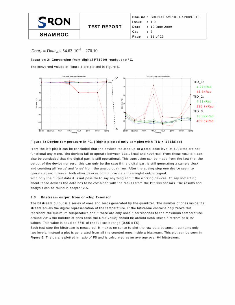
10.2701063.54 3 −⋅×= −lsbC DoutDout
Equation 2: Conversion from digital PT1000 readout to °C.
The converted values of Figure 4 are plotted in Figure 5.
Figure 5: Device temperature in °C. (Right: plotted only samples with TID < 136kRad)
From the left plot it can be concluded that the devices radiated up-to a total dose level of 409kRad are not
functional any more. The devices fail to operate between 135.7kRad and 409kRad. From these results it can
also be concluded that the digital part is still operational. This conclusion can be made from the fact that the
output of the device not zero, this can only be the case if the digital part is still generating a sample clock
and counting all 'zeros' and 'ones' from the analog quantizer. After the ageing step one device seem to
operate again, however both other devices do not provide a meaningful output signal.
With only the output data it is not possible to say anything about the working devices. To say something
about those devices the data has to be combined with the results from the PT1000 sensors. The results and
analysis can be found in chapter 2.5.
2.3 Bitstream output from on-chip T-sensor
The bitstream output is a series of ones and zeros generated by the quantizer. The number of ones inside the
stream equals the digital representation of the temperature. If the bitstream contains only zero's this
represent the minimum temperature and if there are only ones it corresponds to the maximum temperature.
Around 20°C the number of ones (also the Dout value) should be around 5300 inside a stream of 8192
values. This value is equal to 65% of the full scale range (0.65 x FS).
Each test step the bitstream is measured. It makes no sense to plot the raw data because it contains only
two levels, instead a plot is generated from all the counted ones inside a bitstream. This plot can be seen in
Figure 6. The data is plotted in ratio of FS and is calculated as an average over 64 bitstreams.
TID_1:
1.97kRad
43.8kRad
TID_2:
4.11kRad
135.7kRad
TID_3:
16.32kRad
409.5kRad

SHAMROC
TEST REPORT
Doc. no. : SRON-SHAMROC-TR-2009-010
Issue : 1.0
Date : 12 June 2009
Cat : 3
Page : 12 of 23
Figure 6: Ratio of Full Scale calculated from the bitstream data (Right: only with TID < 136kRad).
The plot is quite similar to the plot made from the Dout data. This is as expected due to the radiation
hardness of the digital part. To formulate a good conclusion about the relation between the bitstream and the
Dout value the ratio between them should be calculated. This is done in section 2.4 of this report.
Since the mean value is calculated over 64 bitstreams the noise of these streams can also be calculated. The
noise is represented as a peak to peak value in Figure 7.
Figure 7: peak to peak noise calculated from the bitstream data (only with TID < 136kRad).
The mean levels of each separate bitstream do not differ a lot from each other. If the total number of ones is
only one more this will result is a peak to peak value of 1/8192 (0.12·10-3). From the plot it can be concluded
that the noise becomes slightly more as function of radiation. This increase in noise is however small with
respect to the change in readout value.
2.4 Ratio between bitstream and Dout
The ratio between the bitstream output and the Dout value should be constant since the ratio between these
to data sets is on a digital counter. The ratio between the two datasets is calculated and plotted in Figure 8.
This level corresponds to only 1 extra '1'
between bitstreams
TID_1:
1.97kRad
43.8kRad
TID_2:
4.11kRad
135.7kRad
TID_3:
16.32kRad
409.5kRad
TID_1: TID_2: TID_3:
1.97kRad 4.11kRad 16.32kRad
43.8kRad 135.7kRad 409.5kRad

SHAMROC
TEST REPORT
Doc. no. : SRON-SHAMROC-TR-2009-010
Issue : 1.0
Date : 12 June 2009
Cat : 3
Page : 13 of 23
Figure 8: Ratio between bitstream and Dout.
From the figure can be seen that the ratio is in fact not a constant factor. The difference in the ratio can be
explained by the fact that the bitstream and the Dout value are not read simultaneously. This will result in a
slightly different input temperature, which results in a ratio difference. The ratio differences are not subject
to radiation since the red lines have the same spread as the reference device (blue line). The ratio measured
at the 'ageing' test step can be a result of radiation. This is however hard to verify since analog part is
almost completely broken and may therefore not be seen as a accurate input source for the digital part.
2.5 Ratio between Dout and PT1000
Due to the fact that the input level (temperature) is not equal in all test situations it is hard to formulate
conclusions about the device output. In order to gain more knowledge about the influence of radiation the
data obtained from each device is divided by the temperature obtained from the PT1000 sensor. This results
in a ratio value which should be constant. The results can be found in Figure 9 up-to Figure 12.
Figure 9: Ratio between PT1000 and Dout.
In Figure 9 it can be seen that, due to the failure of the test board at '@ESTEC', the ratio is also not correct.
The data is plotted in Figure 10 without the '@ESTEC' data points to get a better view at the other data
points.
For zoom see Figure 10
Theoretical ratio between bitstream and Dout (213 = 8192)
TID_1: TID_2: TID_3:
1.97kRad 4.11kRad 16.32kRad
43.8kRad 135.7kRad 409.5kRad
TID_1: TID_2: TID_3:
1.97kRad 4.11kRad 16.32kRad
43.8kRad 135.7kRad 409.5kRad

SHAMROC
TEST REPORT
Doc. no. : SRON-SHAMROC-TR-2009-010
Issue : 1.0
Date : 12 June 2009
Cat : 3
Page : 14 of 23
Figure 10: Ratio between PT1000 and Dout, @ESTEC excluded from the plot.
From this figure it can be seen that the high dose rate devices (red lines inside the plots) definitely change
as function of radiation. A clear influence for all high dose rate devices can already be seen at measurement
point TID_2 (135.7kRad). In order to see if the low dose rate devices (green lines inside the plots) also
change due to radiation a new plot is generated with only the low dose rate devices and the two devices
radiated up-to 136.7kRad. The results can be found in Figure 11.
Figure 11: Ratio between PT1000 and Dout, no @ESTEC data, only samples with TID < 136kRad.
From this plot it can be seen that the high dose rate devices already start to drift at TID_1 measurement
(43.8kRad). When the high dose rate devices are not radiated for the 3rd time they seem to operate again
better (test step TID_3). However, the functionality is still much worse than that it should be. For the low
dose rate devices no drift can be observed as a result of radiation. This is even better visible in Figure 12.
For zoom see Figure 11
For zoom see Figure 12
TID_1: TID_2: TID_3:
1.97kRad 4.11kRad 16.32kRad
43.8kRad 135.7kRad 409.5kRad
TID_1: TID_2: TID_3:
1.97kRad 4.11kRad 16.32kRad
43.8kRad 135.7kRad 409.5kRad

SHAMROC
TEST REPORT
Doc. no. : SRON-SHAMROC-TR-2009-010
Issue : 1.0
Date : 12 June 2009
Cat : 3
Page : 15 of 23
Figure 12: Ratio between PT1000 and Dout, no @ESTEC data, only samples with TID < 16.3kRad.
This figure shows that the low dose rated devices have the same 'spread' as the reference device, which is
not radiated at all.
2.6 Bitstream spectrum
From the series of ones and zeros a spectrum can be calculated. The calculated spectrum is averaged over
the 64 readout streams. The result is plotted in Figure 13 where the lines colours correspond to Table 1.
Figure 13: bitstream spectrum averaged 64 times. (Fquantizer = 11.236kHz).
From the figure it can be concluded that already in test step 'TID_1' (T20) the red lines are starting to drift
from the other lines (see ). This is most likely the result of the radiation. At point 'TID_2' (T30) the
radiation dose is even higher and the lines are also worse (see ).
At T40 and higher the spectrum is completely disturbed for the high dose rate devices. The only frequency in
the bitstream is half the sample frequency. This is due to the fact that the bitstream corresponds to a series
of 1-0-1-0-1-etc.
TID_1: TID_2: TID_3:
1.97kRad 4.11kRad 16.32kRad

SHAMROC
TEST REPORT
Doc. no. : SRON-SHAMROC-TR-2009-010
Issue : 1.0
Date : 12 June 2009
Cat : 3
Page : 16 of 23
3 Power consumption
The power consumption of the on-chip T-sensor is measured during each measurement step. The power is
calculated by measuring the voltage and current of the analog supply, the digital supply and the IO supply.
This is done for the 'ON'-state of the on-chip T-sensor as well as the 'OFF'-state. Each voltage and current is
measured for 10 samples in the 'ON'-state with a sample period of 0.5 seconds (2 Hz). After 10 samples the
on-chip T-senor is set to the 'OFF'-state and again 10 samples are measured. The raw data samples are
plotted in Appendix A, Figure 21 up-to Figure 26. The data is plotted against time for each individual
measurement step.
3.1 Analog power
The analog power is calculated during the 'ON' and the 'OFF'-state by multiplying the measured analog
voltage with the measured analog current. The result is plotted in Figure 14.
Figure 14: Analog power consumption during the 'ON'- (left) and 'OFF'-state (right).
From the 'ON'-state it can be seen that the power consumption increases a lot after a total dose of
135.7kRad (red data at TID_2). The nominal 'ON'-power is about 1.5mW while the power for the high dose
rate devices is increased up to 2.5mW. The first power increase in the 'OFF'-state is visible at TID_3
(409kRad). The power is increased from 0.55mW up to 0.75mW (average increase; 0.9mW maximum). The
'OFF'-increase is only visible for the devices which are radiated at a high dose rate for the 3rd time. The two
devices which are only radiated up to 135.7kRad do not show any change when the samples are measured at
test step TID_3. This is also as expected since nothing happened between those two measurement steps.
Measurement TID_3 for sample 6210T-1014 (marked with: ) might be a bad measurement, since the
measurement @SRON is much lower and the only action performed on the samples between those two steps
is the transportation from ESTEC to SRON. There might be some annealing effect as well during this period,
but the other two samples do not show anything like that so this is not very likely. For the low dose rate
samples no effects can be observed.
3.2 Digital Power
The digital power is calculated during the 'ON' and the 'OFF'-state by multiplying the measured digital voltage
with the measured digital current. The result is plotted in Figure 15.
TID_1:
1.97kRad
43.8kRad
TID_2:
4.11kRad
135.7kRad
TID_3:
16.32kRad
409.5kRad

SHAMROC
TEST REPORT
Doc. no. : SRON-SHAMROC-TR-2009-010
Issue : 1.0
Date : 12 June 2009
Cat : 3
Page : 17 of 23
Figure 15: Digital power consumption during the 'ON'- (left) and 'OFF'-state (right).
From the digital measurement it can be concluded that the power is slightly increased during the 'ON'-state
of the chip. The increase is limited to 30µW above the nominal level of 0.3mW. The power increase is
measured at a dose level of 409kRad. After the ageing step the power consumption is again back to its
nominal level. The digital 'OFF'-power is again strange for sample 6210T-1014 (marked with: ). Again the
measured power is higher than expected from the other results. For the low dose rate samples again no
influence is measured. The increase in digital power might be a direct cause of the increase in digital activity.
Due to the failure of the analog part of the chip the output of the chip is a toggling bitstream (1-0-1-0-1-…).
Such a toggling bitstream consumes more digital power.
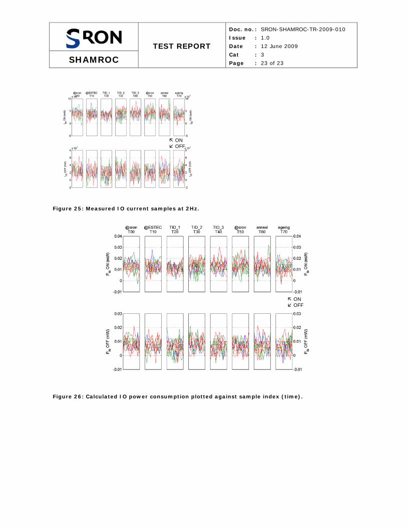
3.3 IO Power
The IO power is calculated during the 'ON' and the 'OFF'-state by multiplying the measured IO current with
3.3V. The calculation is done with a fixed value of 3.3V since it is not possible to measure the IO voltage
automatically with this test board. The results of the power calculation are plotted in Figure 16.
Figure 16: IO power consumption during the 'ON'- (left) and 'OFF'-state (right).
From the figure it can be seen that no influence of radiation can be observed in the IO power consumption.
This is true for the low dose rate devices as well as the high dose rate devices.
TID_1:
1.97kRad
43.8kRad
TID_2:
4.11kRad
135.7kRad
TID_3:
16.32kRad
409.5kRad
TID_1:
1.97kRad
43.8kRad
TID_2:
4.11kRad
135.7kRad
TID_3:
16.32kRad
409.5kRad
SHAMROC
TEST REPORT
Doc. no. : SRON-SHAMROC-TR-2009-010
Issue : 1.0
Date : 12 June 2009
Cat : 3
Page : 18 of 23
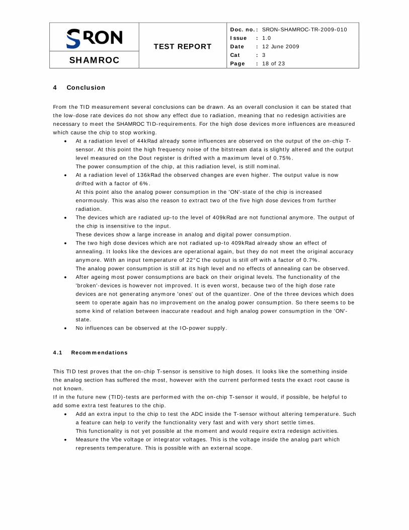
4 Conclusion
From the TID measurement several conclusions can be drawn. As an overall conclusion it can be stated that
the low-dose rate devices do not show any effect due to radiation, meaning that no redesign activities are
necessary to meet the SHAMROC TID-requirements. For the high dose devices more influences are measured
which cause the chip to stop working.
• At a radiation level of 44kRad already some influences are observed on the output of the on-chip T-
sensor. At this point the high frequency noise of the bitstream data is slightly altered and the output
level measured on the Dout register is drifted with a maximum level of 0.75%.
The power consumption of the chip, at this radiation level, is still nominal.
• At a radiation level of 136kRad the observed changes are even higher. The output value is now
drifted with a factor of 6%.
At this point also the analog power consumption in the 'ON'-state of the chip is increased
enormously. This was also the reason to extract two of the five high dose devices from further
radiation.
• The devices which are radiated up-to the level of 409kRad are not functional anymore. The output of
the chip is insensitive to the input.
These devices show a large increase in analog and digital power consumption.
• The two high dose devices which are not radiated up-to 409kRad already show an effect of
annealing. It looks like the devices are operational again, but they do not meet the original accuracy
anymore. With an input temperature of 22°C the output is still off with a factor of 0.7%.
The analog power consumption is still at its high level and no effects of annealing can be observed.
• After ageing most power consumptions are back on their original levels. The functionality of the
'broken'-devices is however not improved. It is even worst, because two of the high dose rate
devices are not generating anymore 'ones' out of the quantizer. One of the three devices which does
seem to operate again has no improvement on the analog power consumption. So there seems to be
some kind of relation between inaccurate readout and high analog power consumption in the 'ON'-
state.
• No influences can be observed at the IO-power supply.
4.1 Recommendations
This TID test proves that the on-chip T-sensor is sensitive to high doses. It looks like the something inside
the analog section has suffered the most, however with the current performed tests the exact root cause is
not known.
If in the future new (TID)-tests are performed with the on-chip T-sensor it would, if possible, be helpful to
add some extra test features to the chip.
• Add an extra input to the chip to test the ADC inside the T-sensor without altering temperature. Such
a feature can help to verify the functionality very fast and with very short settle times.
This functionality is not yet possible at the moment and would require extra redesign activities.
• Measure the Vbe voltage or integrator voltages. This is the voltage inside the analog part which
represents temperature. This is possible with an external scope.

SHAMROC
TEST REPORT
Doc. no. : SRON-SHAMROC-TR-2009-010
Issue : 1.0
Date : 12 June 2009
Cat : 3
Page : 19 of 23
Appendix A
RAW data files.
Figure 17: Measured temperature with PT1000 sensor sampled at 1Hz.
Figure 18: Measured temperature with PT1000 sensor sampled at 1Hz (plotted without T10).

SHAMROC
TEST REPORT
Doc. no. : SRON-SHAMROC-TR-2009-010
Issue : 1.0
Date : 12 June 2009
Cat : 3
Page : 20 of 23
Figure 19: Measured temperature on Dout. (sampled at 1Hz)
Figure 20: Measured temperature on Dout. (Fs = 1Hz, plotted devices with TID <136kRad)

SHAMROC
TEST REPORT
Doc. no. : SRON-SHAMROC-TR-2009-010
Issue : 1.0
Date : 12 June 2009
Cat : 3
Page : 21 of 23
Figure 21: Measured analog current (left) and analog voltage (right) samples at 2Hz.
Figure 22: Calculated analog power consumption plotted against sample index (time).
ON OFF
ON and OFF
ON OFF

SHAMROC
TEST REPORT
Doc. no. : SRON-SHAMROC-TR-2009-010
Issue : 1.0
Date : 12 June 2009
Cat : 3
Page : 22 of 23
Figure 23: Measured digital current (left) and analog voltage (right) samples at 2Hz.
Figure 24: Calculated digital power consumption plotted against sample index (time).
ON OFF
ON and OFF
ON OFF
SHAMROC
TEST REPORT
Doc. no. : SRON-SHAMROC-TR-2009-010
Issue : 1.0
Date : 12 June 2009
Cat : 3
Page : 23 of 23
Figure 25: Measured IO current samples at 2Hz.
Figure 26: Calculated IO power consumption plotted against sample index (time).
ON OFF
ON OFF