Embed Size (px)
Citation preview

AN ABSTRACT OF THE DISSERTATION OF
Chengwei Zhang for the degree of Doctor of Philosophy in Electrical and Computer
Engineering presented on December 3, 2003
Title: Timing Jitter and Phase noise in Electronic Oscillators
Abstract approved:
Leonard Forbes
In the first part of this dissertation, low frequency l/f or flicker noise in the frequency
range of Hz to kHz has been identified and demonstrated to be described by
temperature fluctuations in heat conduction in bipolar transistors operated at higher
power densities. This noise phenomenon is not described by current SPICE programs
used in circuit simulations. This noise in the kHz range can modulate LC oscillators
and can be the determining factor in causing phase noise in modern wireless
communication systems. At lower frequencies or lower power densities flicker noise
may still result from number fluctuations or mobility fluctuations but this is not as
important in determining the phase noise at kHz offsets from the carrier frequencies.
In the second part of this dissertation work, we have developed a large signal non-
linear transient simulation technique to simulate phase noise due to device noise in
electronic oscillators. Simulation results are consistent with Leeson’s theory and the
magnitude of the sidebands directly scales with the magnitude of injected noise.
Simulation also shows phase noise at 4.7 MHz frequency offset is white noise

dominated and in good agreement with the experimental data reported in the
literature.
In the third part of this dissertation work, we have developed a large signal non-
linear transient simulation technique to simulate timing jitter in electronic oscillators.
Simulation results are consistent with the accepted theory, analytical formula and
A.Hajimiri's analytical model for white noise. Two important parameters cycle jitter,
and cycle to cycle jitter used to describe jitter performance can be obtained from
simulation. Simulation results are also compared with measurement and close
agreement was observed between them.
We have employed this methodology and investigated the timing jitter in silicon BJT
/or SiGe HBT ECL ring oscillators, and we have shown silicon BJT /or SiGe HBT
ring oscillators have lower jitter compared to their CMOS counterparts. As such
silicon BJT and/or SiGe HBT ring oscillators are a potential choice for low jitter
applications.

Copyright by Chengwei ZhangDecember 3, 2003
All Rights Reserved
Timing Jitter and Phase Noise in Electronic Oscillators
by
Chengwei Zhang
A DISSERTATION
submitted to
Oregon State University
in partial fulfillment ofthe requirements for the
degree of
Doctor of Philosophy
Presented December 3, 2003Commencement June, 2004

Doctor of Philosophy dissertation of Chengwei Zhang presented on December 3,2003
APPROVED:
_________________________________________________________Major Professor, representing Electrical and Computer Engineering
_________________________________________________________Director of School of Electrical Engineering and Computer Science
_________________________________________________________Dean of Graduate School
I understand that my dissertation will become part of the permanent collection ofOregon State University libraries. My signature below authorizes release of mydissertation to any reader upon request.
____________________________________________________________Chengwei Zhang, Author

ACKNOWLEDGEMENT
I would like to express my sincere and deep appreciation to my academic advisor,
Professor Leonard Forbes, for his guidance and encouragement throughout my study
at Oregon State University. His guidance is a great help in the progress of finishing
this research and dissertation work
I also would like to thank Professor S. Subramanian for being my minor professor
and his wonderful teaching on the electronic materials and device courses.
I would like to thank Professor Raghu Settaluri, Professor Molly Shor, Professor
Thomas G. Dietterich for spending their valuable time as my committee members.
Thanks to Center for Design of Analog-Digital Integrated Circuits (CDADIC) for
financial support during my study here.
Thanks to Teradyne Inc. for providing measurement data of nine stage differential
CMOS ring oscillator.
Thanks to my group members, Mark Chen, Ling Li, Junlin Zhou, Binglei Zhang, I.
Chandra, Xinyu Wang for their help on my research work.
This dissertation is dedicated to my parents, Jingsun Zhang and Xiuxian Zhong, my
dear wife, Xiumei Wu for their constant encouragement and support throughout my
study towards this Ph.D degree.

TABLE OF CONTENTS
Page
1. INTRODUCTION…………………………………………………………… 1
2. NOISE MODELS IN CMOS AND BJT DEVICES………………………… 6
2.1 Current Noise Models in CMOS and BJT Devices……………………. 6
2.2 1/f Noise Due to Temperature Fluctuations in Heat Conduction in
Bipolar Transistors……………………………………………………… 8
3. MODELING OF RANDOM PHASE FLICKER NOISE AND WHITENOISE………………………………………………………………………... 22
4. PHASE NOISE IN A 2-G HZ BJT LC OSCILLATOR……………………… 24
4.1 Characterization of Phase Noise………………………………………… 24
4.2 Simulation of Phase Noise in LC BJT Oscillator……………………….. 25
4.3 Simulation Results and Discussion……………………………………… 28
5. TIMING JITTER IN SINGLE ENDED CMOS RING OSCILLATORS…….. 34
5.1 Definitions of Timing Jitter……………………………………………… 34
5.2 Stationary Approach in Single Ended CMOS Ring Oscillators…………. 36
5.3 Simulation of Timing Jitter in Single Ended CMOS Ring Oscillators….. 40
5.4 Simulation Results and Discussion……………………………………… 42
TABLE OF CONTENTS (Continued)
Page
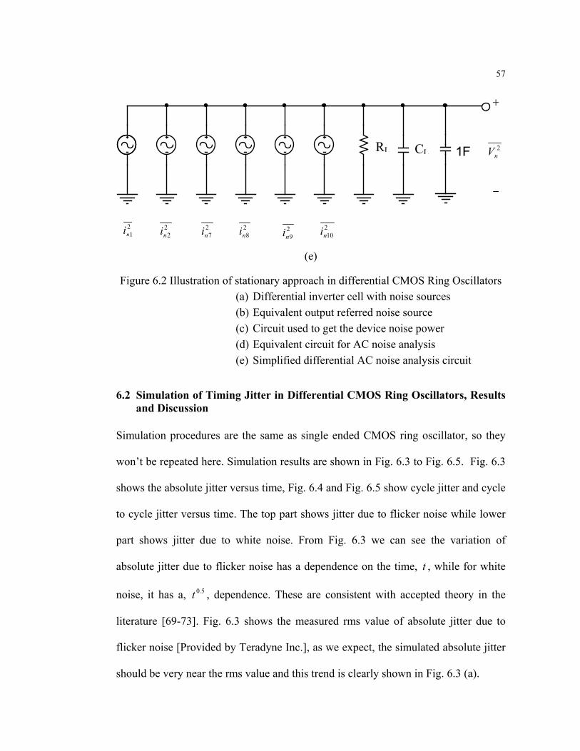
6. TIMING JITTER IN DIFFERENTIAL CMOS RING OSCILLATORS…….. 52
6.1 Stationary Approach in Differential CMOS Ring Oscillators………….. 52
6.2 Simulation of Timing Jitter in Differential CMOS Ring Oscillators,
Results and Discussion………………………………………………… 57
7. TIMING JITTER IN SILICON BJT /OR SIGE HBT ECL RINGOSCILLATORS……………………………………………………………… 62
7.1 Stationary Approach in Silicon BJT /OR SiGe HBT ECL Ring
Oscillators………………………………………………………………. 62
7.2 Simulation of Timing Jitter in Silicon BJT /OR SiGe HBT ECL Ring
Oscillators, Results and Discussion…………………………………….. 65
8. CONCLUSION………………………………………………………………. 69
BIBLIOGRAPHY………………………………………………………………… 72
APPENDICES……………………………………………………………………. 80
LIST OF FIGURES
Figure Page
2.1 Power dissipation in a transistor and heat conduction model in spherical 9 coordinates 2.2 Steady state heat conduction due to power dissipation in the transmission 13 line model
2.3 Measured base-emitter voltage VBE at VCE =1V and VCE =15V with 19 different ambient temperatures for IC=10mA and IC=30mA respectively 2.4 Measured current noise power at f=1Hz versus (∆T/T)2 for VCE=15V and 20 IC=10mA and 30mA respectively.
2.5 A comparison between mean square collector noise current measured 21on a bipolar transistor with high power dissipation (VCE=15V, IC=10mA)and that calculated using (∆T/T)2
4.1 Single sideband phase noise to carrier ratio 25
4.2 BJT LC VCO for simulation 27
4.3 Equivalent circuit of the inductor 28
4.4 Simulated output power spectral of LC oscillator 30
4.5 Simulated sideband power below carrier per Hz versus offset from the 31 carrier (fosc=2 GHz)
4.6 Simulated sideband power below carrier per Hz versus injected noise at 32 4.7 MHz offset from carrier frequency
4.7 Projected results with comparison to observed one 33
5.1 Illustration of timing jitter 34
5.2 Illustration of (a) long term jitter and (b) cycle to cycle jitter 36
5.3 Single ended ring oscillator 37

LIST OF FIGURES (continued)
Figure Page
5.4 Illustration of Stationary Approach in Single Ended CMOS Ring 39Oscillators
5.5 Histogram of output clock for noise free case 41
5.6 Absolute jitter as a function of time 43
5.7 Cycle jitter as a function of time 44
5.8 Cycle to cycle jitter as a function of time 45
5.9 Cycle to cycle jitter as a function of injected noise 46
5.10 Comparison between simulated absolute jitter and calculated rms value 49
5.11 RMS absolute jitter versus time for white noise 50
6.1 CMOS differential ring oscillator 52
6.2 Illustration of stationary approach in differential CMOS Ring Oscillators 57
6.3 Absolute jitter as a function of time 59
6.4 Cycle jitter as a function of time 60
6.5 Cycle to cycle jitter as a function of time 61
7.1 Nine stage silicon BJT/or SiGe HBT ECL ring oscillator 63
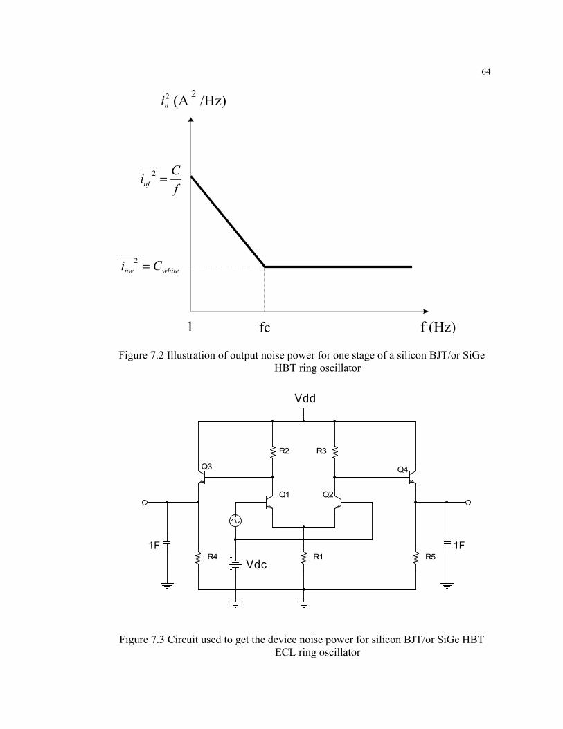
7.2 Illustration of output noise power for one stage of a silicon BJT/or 64 SiGe HBT ring oscillator
7.3 Circuit used to get the device noise power for silicon BJT/or SiGe HBT 64 ECL ring oscillator
7.4 Histogram of silicon BJT ECL ring oscillator clock periods 66

LIST OF FIGURES (continued)
Figure Page
7.5 Absolute jitter as a function of time for silicon BJT ECL ring oscillator 67 due to flicker noise
7.6 Absolute jitter as a function of time for SiGe HBT ECL ring oscillator 68 due to flicker noise

LIST OF TABLES
Table Page
5.1 Relationship between cycle jitter and cycle to cycle jitter for white noise 47
5.2 Comparison of simulation results and A. Hajimiri's analytical model for 51 RMS absolute jitter due to white noise at 1us
6.1 Relationship between cycle jitter and cycle to cycle jitter for white noise 58
7.1 Absolute jitter due to flicker noise at 1us for three different types of oscillator 68

LIST OF APPENDICES
Appendix Page
A Device Noise Measurement 81
B MATLAB Program for Modeling of Random Phase Flicker Noise and White Noise 85
C Procedure of Phase Noise Simulation in Oscillators 92
D Procedure of Timing Jitter Simulation in Oscillators 95

LIST OF APPENDIX FIGURES
Figure Page
A.1 Automated Noise Measurement System 81
A.2 ADC Board Based Noise Measurement System 82

TIMING JITTER AND PHASE NOISE IN ELECTRONICOSCILLATORS
1. INTRODUCTION
Noise is an important design factor in electronic systems, it determines the lower
limit on the level of the signal that can be processed by these devices and circuits. It
is very important to understand the mechanism of noise sources.
Generally, there are two groups of noise sources, which are usually classified as
device noise and interference. Device noise includes thermal, shot and flicker noise,
while interference includes substrate and power supply noise. There is always some
way to alleviate substrate and power supply noise but not for device noise.
Of all the noise sources, the origin of flicker noise, which is also known as 1/f noise
because the noise spectral density is inversely proportional to frequency, is still
unknown. In the past forty years, a large number of papers have been published on
the study of 1/f noise in MOSFET’s and BJT’s [1-46], but controversy still exists and
there is no generally accepted model.
In the case of BJT’s, one of the original references on flicker noise in bipolar
transistors, by E.R. Chenette et al., [43] is still used as the basis for modeling noise
in bipolar transistors. It gives the low frequency l/f or flicker noise as:
fIKi nBn /2 = (1.1)
where K is a constant, IB is the base current, n is a number between one and two, and
f is the frequency. Subsequently the physical mechanism for this noise has been
attributed to either mobility fluctuations, as described by Hooge's empirical formula,
2
and/or surface state effects in the base-emitter junction, there is still no universally
accepted model. An equation of the above form is used in SPICE, PSPICE and
HSPICE models for circuit simulations. However, the original publication [43] also
described a component that depended on, VCE, or the collector emitter voltage,
although no model or equation was given for this component. Recently we have been
able to show that at high power density or high junction temperatures of operation
the 1/f noise varies with power dissipation [45], in particular as the collector current
is held constant and the collector emitter voltage is varied [46]. In these reports,
however, we were there primarily interested in publishing the theoretical results and
showing the functional form of the equation describing the manner in which the 1/f
noise varies. We did not demonstrate a detailed correspondence. In the research
work presented in this dissertation, we will give a detailed comparison between the
theory and the 1/f noise measured on bipolar transistors and show that the low
frequency noise at higher junction temperatures is described by temperature
fluctuations in heat conduction [45,46]. These new results are particularly relevant to
phase noise in voltage-controlled oscillators operating with low base circuit
impedance since they determine the phase noise at kHz offsets from the carrier
frequencies.
Oscillators are integral parts of many electronic applications. For a noise free
oscillator, the output is a perfect timing reference with a periodically time-variant
signal. However, in reality, due to the existence of noise, all oscillators will exhibit
phase noise and timing jitter. Phase noise and timing jitter are the same phenomena

3
except one description is used in the frequency domain and the other is used in the
time domain. Analog and digital designers prefer using phase noise and timing jitter
respectively.
With the fast development of wireless communication, there is an increased demand
for more available channels, thus RF oscillators employed in wireless
communication must meet more stringent requirements for phase noise. The term
phase noise, which is used to describe frequency stability, has been widely studied in
the past [49-56]. There have been some models developed for predicting phase noise
in oscillators, however, those models are based on linear circuit concepts and
oscillators are basically non-linear large signal circuits. The time varying nature of
oscillators and large non-linearity’s have precluded any meaningful application of
techniques based on linear approximations, the simulations must be performed in the
time domain. In this study, we will develop a large signal transient simulation
technique to simulate phase noise due to device noise in a 2-G Hz BJT LC oscillator.
Timing jitter is critical design considerations in nearly every type of digital systems,
especially for some high-speed digital circuits such as microprocessors and
memories. There have been some studies about timing jitter in electronic systems
[57-68], however, none of them describe an efficient technique to simulate jitter.
Although some analytical models have been reported for jitter in oscillators [69-73],
these models have been developed for white noise only while jitter due to 1/f noise is
usually more important since it increases linearly with time. There has been no
simulation technique to predict timing jitter due to flicker noise. The lack of a

4
simulation technique to accurately predict timing jitter makes design of low jitter
systems a problem. In this study, we will try to develop a method to efficiently
simulate timing jitter.
The possible sources of timing jitter are substrate and power supply noise, and
inherent electronic noise of devices such as flicker and white noise. Since there is
always some way to alleviate substrate and power supply noise, in a fully optimized
design the main source of timing jitter is the inherent electronic device noise, in this
work we will only concentrate on jitter due to 1/f and white noise. However, the
method described in this study is also applicable to substrate and power supply noise.
The organization of this dissertation work is as follows, in chapter 2, first we will
give a general review of noise models in CMOS and BJT devices, then we will
describe a new model of 1/f noise in BJT devices based on temperature fluctuations.
In chapter 3, a technique to transform frequency domain noise power into time
domain noise data is introduced.
In chapter 4, phase noise resulting from white and flicker noise in a BJT LC
oscillator is investigated. Large signal transient time domain SPICE simulations of
phase noise resulting from the random-phase flicker and white noise in a 2 GHz BJT
LC oscillator have been performed and demonstrated. The simulation results are
compared with experimental result reported in the literature.
In chapter 5, we are developing an extension of our large signal transient simulation
technique of phase noise to the simulation of timing jitter. Timing jitter due to device
noise in a three stage single ended CMOS ring oscillator is studied, and a

5
methodology to efficiently simulate timing jitter has been developed. Simulation
results are discussed and compared with analytical model.
In chapter 6, we have employed this methodology and simulated timing jitter in a
nine stage differential CMOS ring oscillator, simulation results are discussed and
compared with experimental results.
In chapter 7, we have employed this methodology and investigated the timing jitter
in silicon BJT /or SiGe HBT ECL ring oscillators, and we have shown BJT /or SiGe
HBT oscillators have lower jitter compared to their CMOS counterparts.
In chapter 8, the conclusions are discussed.

6
2. NOISE MODELS IN CMOS AND BJT DEVICES
2.1 Current Noise Models in CMOS and BJT Devices
For active MOSFET transistors, dominant noise sources are flicker and thermal
noise. In HSPICE, channel thermal noise and flicker noise are modeled by a current
source and expressed by the following equations.
For flicker noise,
(i) noimod = 1 noise model
AFeffeffox
mnd fLWC
gKFI⋅⋅⋅
⋅=
22 (2.1)
(ii) noimod = 2 noise model
Iq kT I
C L fNoia
NN
Noib N Nndeff ds
OX effef
ll
22
2 80
14
14 0102 102 10
=•
•+ ×+ ×
+ • −µ
{ log{ } ( )
+ − +•
•+ • + •
+ ×Noic
N NV I L
W L fNoia Noib N Noic N
Nltm ds clm
eff effef
l l
l2 10 2 1002 2
2 8
2
14 2{ )}( )
∆ (2.2)
A noise equation selector parameter noimod is used to select whether noimod=1 or
noimod=2 noise model is used in the small signal AC noise analysis. In noimod=1
noise model, AF is flicker noise exponent which is 1 at default and KF is flicker
noise coefficient. Reasonable values for KF are in the range of 1 x 10-19 to 1 x 10-25
V2F.
For thermal noise in channel,
382 m
ndgkTI ⋅⋅
= (2.3)

7
Noise sources in bipolar transistors include shot noise due to collector and base
currents, which can be modeled as follows
bnb qII 22 = (2.4)
cnc qII 22 = (2.5)
where q is the magnitude of electronic charge (1.6 x 10⁻¹⁹ C), bI is the base current,
cI is the collector current.
Thermal noise of the base resistance, modeled as
bnb kTrV 42 = (2.6)
and the flicker noise of the base current,
fIki nbFn /2 = (2.7)
where KF is a constant, bI is the base current, n is a number between one and two,
and f is the frequency.
The current flicker noise model in bipolar transistors is based upon original work
done in the 1963 time frame [43]. At that time and given the state of technology with
only poor surface passivation techniques, the l/f noise in bipolar transistors was all
attributed to surface effects [1] in the base-emitter junction. This leads to the
commonly used pi-model for noise in bipolar transistors, or Van der Ziel model,
described in most textbooks [48] and circuit simulation programs based on SPICE.
This overlooks the more recent work and perhaps better-accepted model for l/f noise
in that it is not a surface effect but rather a bulk phenomena [3,22] described by

8
Hooge’s equation. Unfortunately, Hooge’s equation is only an empirical one. In the
following, we will introduce a new flicker noise model, which is described by
temperature fluctuations in heat conduction.
2.2 1/f noise Due to Temperature Fluctuations in Heat Conduction in BipolarTransistors
2.2.1 Theory
The R-C transmission lines previously analyzed [45,46] are diffusion lines and
potential and currents are described by the diffusion equation;
∂∂
∂∂
2
2
Vx
R C Vt
= (2.8)
This is the same type of equation describing heat conduction [47];
a Tx
Tt
∂∂
∂∂
2
2 = (2.9)
where, a, is the thermal diffusivity, m2/sec in MKS units and, T, is the temperature.
Based on the solution in rectangular coordinates, a mean square fluctuation in the
collector current or mean square noise current equation can be obtained as [46]:
( )
∆
∆=
ωωcth
n TT
qTkVIqi
222
/2 (2.10)
where now,
AKdIVT CE=∆ (2.11)

9
As it turns out the approximation in rectangular coordinates of a plate-wall model is
probably not a good approximation of the actual situation. A more complicated but
better fitting model to the actual situation is one in spherical coordinates which is
analyzed in the following sections. In the spherical coordinates, an equivalent circuit
representation can be made for heat conduction as shown in Fig. 2.1 where for each
volume element,
mWKrR ⋅Κ= /)4(/1 2π (2.12)
mKJrCC p ⋅= /4 2πρ (2.13)
Figure 2.1 Power dissipation in a transistor and heat conduction model in sphericalcoordinates
r2
r1 R
CI
|VCE|
NN+ P
E B C

10
where, K, is the thermal conductivity, Cp , the heat capacity, ρ , the density, and,
4πr2 , the surface area of the sphere whose radius is, r, through which there is heat
conduction. Temperature is analogous to voltage and heat flux analogous to current.
The thermal conductivity and diffusivity are not independent but are related in a
form which we will later find useful,
aC
K mJpΚ
=⋅1 3
ρ(2.14)
The time invariant steady state, or DC, solution for this line when terminated by a
heat sink with infinite heat capacity is then a linear variation in temperature and the
thermal impedance is,
DCS RDCZ =)( ,
121
2
12
2
1 4111
41
41
KrrrKdr
KrRdrR
r
r
r
rDC πππ
≈
−=== ∫∫ (2.15)
Here we assume r2 is infinite. From results shown later we know that, r1 << r2, so
this assumption is reasonable.
The heat flux; drdTrkflux 24π= and for the total line
DCRTflux ∆
= (2.16)
The steady state time dependent solutions of this differential equation and
transmission line, from r1 to r2, in response to a high frequency sinusoidal excitation
in temperature T at the sending end of this line are described by the AC impedance
looking into this line, ZS .

11
A. Solutions with an infinite heat sink
We have previously always assumed an infinite heat sink at the interface between the
device and the outside world. An infinite heat sink is one with infinite heat capacity
or infinite capacitor which acts as a short circuit on the line at all frequencies. At
very low frequencies, then the sending end impedance ZS is just RDC. At higher
frequencies, the sending end impedance is very difficult to calculate and express
using a simple formula. However if frequencies are high enough the line will be a
long lossy line and then the sending end impedance is just Zo, where;
ωπω ja
KrCjR
YZZ O 24
1=== ,
( ) ωωπ 21
2
41
22
12
1 4)()(
raR
rKarZrZ DC
OS === (2.17)
if we let 21ra
cth =ω , then Eqn. (2.17) also can be written as
ωωcthDC
SRrZ
22
1)( = (2.18)
Fig. 2.2(b) shows then the impedance looking into the transmission line with a short
circuit termination with a l/ω1/2 frequency dependence.
B. Solutions without an infinite heat sink
Apparently the assumption or approximation of an infinite heat sink at the interface
between the device and the outside world is probably not a good approximation nor
very representative of the actual situation. The next simplest assumption is one

12
where there is a finite thermal resistance between the device and a large heat sink or
the outside world shown as Rcontact in Fig. 2.2(a) and the heat capacity of the sink is
shown as Csink. If this thermal contact resistance is very high then the line can be
regarded as being open circuited. In this case the temperature fluctuations are
limited by the total heat capacitance of the device,
32
31
32
234)(
344
2
1
rCrrCdrrCC pp
r
rptotal πρπρπρ ≈−== ∫ (2.19)
This will become important at radian frequencies, ωx, which is the corner frequency
between this capacitance and the total DC heat resistance of the sample, RDC:
32
133
234
141
r
ra
rpC
rK
DCRtotalCx ===πρ
πω (2.20)
If ω < ωx, the line appears capacitive, and the sending end impedance is just
ωπρ 3
234
1rC
Zp
S = (2.21)
Fig. 2.2(b) also shows the impedance looking into the transmission line with an open
circuit termination with a 1/ω frequency dependence.
If there is a finite thermal contact resistance Rcontact connected to a large capacity
heat sink, the DC resistance at low frequency will be the sum of the DC thermal
resistance of the line and the contact resistance. While the solutions to the
transmission line equations would be difficult to obtain with this finite termination
they can be estimated as illustrated in Fig. 2.2(b). We can see the transmission line
can be approximated by short-circuited characteristics at high frequencies, which
would result in an approximate, l/ω1/2, frequency dependence of the thermal

13
impedance. Since the noise in the kHz range can modulate LC oscillators and can be
the determining factor in causing phase noise in modern wireless communication
Figure 2.2 Steady state heat conduction due to power dissipation in thetransmission line model

14
systems, and the noise at very low frequencies is not as important, we will just
consider the approximation of short-circuited characteristics of the transmission line.
As is the case with electrical current, which is made up of a large number of
individual events, heat flux is associated with the transfer of energy to lattice
vibrations in discrete elements. We will assume here that the heat energy is
transferred to the lattice over very short time periods in the units of VDC q where VDC
is the applied DC voltage. We are assuming here that the transit time of the electron
through the electron device is small, as is usually the case. Using Carson's theorem,
where the average number of individual events is, N , then;
2)(2)( ωfNfvS
−= (2.22)
if each individual event occurs in a short time then
222)( qVNfS DCv
−
= (2.23)
But the heat flux is just the mean number of individual units of energy times the
energy associated with each, DCqVNflux = . So the spectral intensity of the heat
flux becomes,
22)( nDCv ffluxqVfS == (2.24)
This spectral intensity will cause a mean square temperature variation with spectral
intensity at the surface of the sample given by
222
Snn ZfT = (2.25)

15
again the solution is simple in the two limiting cases; at low frequencies then;
DCDC
DCDC
DC
DCDCn
RTVq
RR
TqV
RfluxqVT
∆=
⋅∆
⋅=
⋅=
2
2
2
2
22
(2.26)
while at high frequencies;
ωωωω
ωω
cthDCDC
cthDC
DCDC
cthDCDCn
RTVq
RR
TqV
RfluxqVT
∆=
⋅⋅
∆⋅=
⋅⋅=
2
2
2
2
22
(2.27)
If the heat source, in Fig. 2.1, is a transistor where the transistor base is by-passed by
a large capacitor to keep the base at a fixed potential then the modulation of the base-
emitter diode temperature will modulate the collector current since
)exp(kTE
kTqVBI GBE −= (2.28)
ITkVqTdTdI )/()/1(/ ∆= (2.29)
where )( BEG V
qEV −=∆ , VBE is the base-emitter junction forward bias voltage and EG
the bandgap energy. The mean square fluctuation in temperature from Eqn. (2.27)
will be determined mostly by power dissipation in the collector-base junction and the
resulting temperature increase, ∆T , and then,

16
∆=
∆⋅=
∆⋅∆=
⋅∆=
ωω
ωωωωωω
cth
cth
DCDC
cthDC
cthDCDCn
TIq
qVNTqV
fluxTTqV
RTqVT
2)()/2(
)(2
2
2
2
2
(2.30)
This results in a mean square fluctuation in the collector current or mean square
noise current.
( )
∆
∆=
⋅∆
=
ωω cth
n
TT
qTkVIq
TIkT
VqT
i
22
2222
2
/2
)(1
(2.31)
where now,
1
1
41
41
KrIV
krqVN
RfluxT
CE
DC
DC
π
π
=
⋅=
⋅=∆
(2.32)
is the temperature increase due mostly to power dissipation in the base-collector
junction, and VCE is the collector-emitter voltage, assuming an infinite heat sink.
2.2.2 Experimental Results
In this study, we used small silicon epitaxial planar common commercial discrete
bipolar transistors, of type npn2222A. In order to generate large power dissipation
which results in a high junction temperature, the devices were operated at high

17
collector currents and high collector-emitter voltages. Next, we determined a way to
measure the temperature increase, ∆T, of the device due to the high power
dissipation. It is well known the base-emitter voltage, VBE, of bipolar transistor
exhibits a negative temperature coefficient, TC. So if we can get the temperature
coefficient, TC, then we can get the temperature increase, ∆T, from the measured
value of VBE. Since the power dissipation of a diode-connected bipolar transistor is
small, the junction temperature will be approximately the ambient temperature. We
first measured the VBE of a diode-connected bipolar transistor, for the simplicity we
just fix the VCE at 1V with different ambient temperatures. The results are shown in
Fig. 2.3. We get the temperature coefficient TC as being -1.4mV/K for IC=10mA
and -1.2mV/K for IC=30mA respectively. The graphs of VBE measured at different
ambient temperatures with VCE=15V are also shown in Fig. 2.3, first for IC=10mA
and then for IC=30mA. From the difference in VBE between VCE=1V and VCE=15V,
we can calculate the temperature increase, ∆T. For example, ∆T is approximately
17 oC for IC=10mA, VCE=15V. If we assume an infinite heat sink and use Equation
(2.32), we get r1=4.6834x10⁻⁴cm, which is a reasonable value for these bipolar
transistors. However, the actual value of r1 is probably larger than this value and the
thermal impedance of the sample is small and the total thermal impedance limited by
the contact impedance.
Finally, we determine from experiment whether 1/f noise has dependence on (∆T/T)2
by holding the collector current and the collector-emitter voltage constant and
measuring the collector current noise under different ambient temperatures such as in

18
air, in home-temperature water, in hot water, and in dry ice. Fig. 2.4 shows the
measured collector current noise versus (∆T/T)2 at f=1.0Hz first for IC=10mA and
then for IC=30mA. From this figure, we can see the trend lines fit the experimental
data very well. This serves to verify our theory and the dependence of noise power
on temperature increase and power dissipation.
Fig. 2.5 shows the automated measurement results of the device noise spectral
density at IC=10mA and VCE =15V. The low frequency measurements are done using
the techniques described previously [46]. At higher frequencies a newer faster
analog to digital converter board, ADC board, has been used for the measurements.
These results are also shown in this figure, which indicates an agreement between
the two measurement results and previous measurement results [46]. Eqn. (2.31) has
been used to calculate the mean square collector noise current at frequencies less
than, ωcth , assuming that the factors limiting the temperature increase are the
external thermal contact resistance.

19
Figure 2.3 Measured base-emitter voltage VBE at VCE =1V and VCE =15V with
different ambient temperatures for IC=10mA and IC=30mA respectively

20
Figure 2.4 Measured current noise power at f=1Hz versus (∆T/T)2 for VCE=15V andIC=10mA and 30mA respectively

21
Figure 2.5 A comparison between mean square collector noise current measured ona bipolar transistor with high power dissipation (VCE=15V, IC=10mA) and
that calculated using (∆T/T)2.

22
3. MODELING OF RANDOM PHASE FLICKER NOISE AND WHITENOISE
The flicker noise and white noise are modeled as
fCinf =2 (3.1)
whitenw Ci =2 (3.2)
where C is the noise power for flicker noise at 1 Hz, whiteC is the white noise power.
We can use Eqn.(3.1) and Eqn.(3.2) to describe different power spectral density
values of flicker or white noise in a range of frequencies with a step frequency, fs.
Then the amplitudes of current components, Iamp (A), associated with the flicker
noise or white noise can be calculated by the following equations:
2122
12 )()( nwwhitenfflick iIoriI == (3.3)
21
21
)()( swhiteampsflickamp fIIorfII •=•= (3.4)
An ideal sinusoidal current signal can then be expressed as
)]()(2sin[)()( itifiIampiInd Φ+•= π (3.5)
where Φ(i) is the random phase, f is frequency, i is the index of the frequency, which
changes from 1 to the end of the frequency range used in the simulation.
The “rand” function in MATLAB is used to create a pseudo-random Φ(i), by using
randomly created internal data in the computer. Then all the individual current

23
components, Ind(i), are summed together to get the random-phase flicker noise,
Iflick’, or random-phase white noise, Iwhite’, in the defined frequency range.
)(')(' iIndIoriIndI whiteflick Σ=Σ= i=range of the frequencies (3.6)

24
4. PHASE NOISE IN A 2-G HZ BJT LC OSCILLATOR
4.1 Characterization of Phase Noise
Frequency stability is an important factor for an oscillator maintaining the same
value of frequency over a given time. The term phase noise is commonly used for
describing short noise random frequency fluctuations of a signal. The definition of
phase noise is shown as follows. The output of an ideal sinusoidal oscillator may be
expressed as:
)2sin()0()( ftVtV π•= (4.1)
where V(0) is the nominal amplitude of the signal, and f is the nominal frequency of
oscillation. In a practical oscillator, the output is more generally given by
)](2sin[)](1[)0()( tqfttAVtV +•+•= π (4.2)
where A(t) and q(t) are the amplitude and phase fluctuation of the signal
respectively. Usually white, or frequency independent, and flicker (1/f) noise are the
generating sources of phase noise. Since all practical oscillators employ some kind of
amplitude-limiting mechanism, most oscillators operate in saturation region with the
amplitude noise component 20 dB lower than the phase noise component, so usually
it is phase noise dominated, we will assume that A(t)<<1 [49] and only study phase
noise.
Phase noise is usually expressed as Single Side Band (SSB) power, which is the ratio
of power in one phase modulation sideband per Hertz bandwidth, at an offset f

25
(frequency) Hertz away from the carrier, to the total signal power. If given
logarithmically, phase noise is expressed in dB relative to the carrier per Hz
bandwidth as dBc/Hz.
s
ssbc P
PfS log10)( = (4.3)
where Ps is the carrier power and Pssb is the sideband power in one Hz bandwidth at
an offset frequency of f from the center (Fig. 4.1) [53].
Figure 4.1 Single sideband phase noise to carrier ratio [53].
4.2 Simulation of Phase Noise in LC BJT Oscillator
Instead of using a conventional SPICE model f
IKFiAFB
nf =2 for describing the
flicker noise, we recently have been able to show that the flicker noise in a bipolar
Amplitude
Frequency
f 0SC
s
ssbc P
PfS =)(
ssbP
sp
f

26
transistor with a low impedance between the base and emitter can be expressed in the
following form [46],
)(22
ffqIi c
Cnf = (4.4)
where IC is the collector current. The corner frequency, fc, is defined as the
frequency at which the flicker noise 2nfi is equal to the collector current shot noise or
white noise Cnw qIi 22 = in a bipolar transistor. Different corner frequencies will cause
different amplitudes of flicker noise. Here we use fc=36kHz such as we have more
recently measured [46] for a typical small bipolar device.
The circuit used in our simulation is based on a low phase noise LC BJT voltage
controlled oscillator introduced by Zannoth etc [56], carrier frequency is 2-GHz. The
circuit diagram is shown in Fig.4.2. The design is based on a LC-resonator with
vertical-coupled inductors, the equivalent circuit of the coupled inductor is shown in
Fig.4.3, which is used as a subcircuit in the HSPICE simulation.
In our simulation, the random-phase flicker noise Iflick’, or random-phase white noise
Iwhite’, obtained from MATLAB, is injected into the signal path as a piece wise linear
waveform at the collector of q4. After that, a transient analysis is performed for the
oscillator with the flicker or white noise source over a relatively large number of
oscillation periods and the output is written as a series of points equally spaced in
time. The internal FFT function in HSPICE is used to compute the FFT of HSPICE
simulation output in the time domain. To get the best results, a Blackman-Harris
window with 16384 points, NP=16384, is used in the FFT analysis. In the
simulation, FFT analysis is starting from 19.56 ns to exclude the starting period that

27
is not oscillating. Simulation shows this period distorts the FFT output very much,
thus has to be excluded. [Detailed procedure of phase noise simulation in Oscillators
is in Appendix C]
Figure 4.2 BJT LC VCO for simulation [56]
Vbias
VCC
Q4 Q3
Q2 Q1
R2 60R1 60
Iosc
C2
1.5p
C1
2p
C4
2p
R3
1k
R4
1k
C3
1.5p
Inoise
.
. .
.k kOut Outx

28
Figure 4.3 Equivalent circuit of the inductor [56]
4.3 Simulation Results and Discussion
Five different conditions of random-phase flicker or white noise, including one
without added noise, are applied to the LC oscillator. Fig.4.4 shows the simulated
output power spectral corresponding to these five different conditions, Fig.4.4 (a) for
injected flicker noise, while Fig.4.4 (b) for injected white noise, these correspond to
five different fc values or white noise sources. It can be seen that when there is no
random-phase noise introduced into the oscillator, the sideband harmonics with
peaks exist, while as the random-phase noise is injected and noise increases, these
1M
Rsub
200
Rsub280
Rsub280
Rs
4.2
100
Rs
4.2
Rsub
200
Cox800 f FCox 800 f F
L2 2.7nH
L1 2.7nH
Cox800 f F
Cc600 f F
Cox 800 f F
Cc 600 f F.
.
K 0.85

29
harmonics are gradually buried in the additional noise. The sideband power increases
with the amplitude of the injected noise.
Fig.4.5 (a) shows the phase noise sideband power spectra density for flicker noise
with four different fc values, while Fig.4.5 (b) for white noise with four different
noise sources. According to Leeson’s theory, phase noise resulting from flicker noise
has a 1/f3 dependence, while from white noise has a 1/f2 dependence on offset
frequency. These 1/f3 and 1/f2 dependencies are clearly shown in Fig.4.5.
Fig.4.6 shows the phase noise sideband power below carrier per Hz (dBc/Hz) versus
injected flicker noise or white noise at 4.7 MHz offset from carrier frequency. It is
clearly from Fig.4.6 that the magnitude of the sideband directly scales with the
magnitude of injected noise. By projecting back to the actual case of the simulated
circuit, which is fc=36.232 kHz and white noise 2qIC=1.1×10⁻²¹ A2/Hz, we obtain the
phase noise at 4.7 MHz offset resulting from flicker noise is -150.7 dBC/Hz, from
white noise is –132 dBc/Hz. At this point it is white noise dominated. The simulation
results are in good agreement with the experimental value of –136 dBc/Hz at this
offset frequency reported in the literature by Zannoth and Kolb [56].
Fig.4.7 shows the projected results with comparison to observed one, it is shown
they match each other and our simulation is able to predict phase noise correctly.

30
(a)
(b)
Figure 4.4 Simulated output power spectral of LC oscillator
(a) flicker noise with different fc values A. fc=400 GHz B. fc=40 GHzC. fc=400 MHz D. fc=4 MHz
E. No flicker noise injected(b) white noise with different noise sources
A. white noise=1.1×10⁻¹⁴ A2/Hz B. white noise=1.1×10⁻¹⁶ A2/HzC white noise=1.1×10⁻¹⁸ A2/Hz D. white noise=1.1×10⁻²⁰ A2/Hz
E. No white noise injected

31
(a)
(b)
Figure 4.5 Simulated sideband power below carrier per Hz versus offset from thecarrier (fosc=2 GHz)
(a) flicker noise with different fc values A. fc=400 GHz B. fc=40 GHzC. fc=400 MHz D. fc=4 MHz
(b) white noise with different noise sourcesA. white noise=1.1×10⁻¹⁴ A2/Hz B. white noise=1.1×10⁻¹⁶ A2/HzC white noise=1.1×10⁻¹⁸ A2/Hz D. white noise=1.1×10⁻²⁰ A2/Hz

32
(a)
(b)
Figure 4.6 Simulated sideband power below carrier per Hz versus injected noise at4.7 MHz offset from carrier frequency
(a) versus fc values (injected flicker noise)(b) versus white noise sources(injected white noise)
-160
-150
-140
-130
-120
-110
-100
-90
-80
1.00E-02 1.00E-01 1.00E+00 1.00E+01 1.00E+02 1.00E+03 1.00E+04 1.00E+05 1.00E+06
1/f noise corner frequency fc (MHz)
Side
band
bel
ow C
arri
er p
er H
z (d
Bc/
Hz) 4.7 MHz offset from
carrier frequency
(36.232kHz, -150.7dBc/Hz)
10-2 10-1 106105104103102101100
-150
-140
-130
-120
-110
-100
-90
-80
-70
-60
-50
1.00E-23 1.00E-21 1.00E-19 1.00E-17 1.00E-15 1.00E-13 1.00E-11
White noise (A2/Hz)
Side
band
bel
ow C
arri
er p
er H
z (d
Bc/
Hz)
(1.1x10⁻²¹ A2/Hz, -132dBc/Hz)
4.7 MHz offset from carrier frequency
10-23 10-21 10-1510-1710-19 10-1110-13

33
Phase Noise (dBc/Hz)
•
4.7MHz
Figure 4.7 Projected results with comparison to observed one
Offset Frequency
-150.7dBc/Hz
Simulated
due to 1/f noise
Observed-136dBc/Hz
Simulated dueto white noise-132dBc/Hz
1/f3
1/f2

34
5. TIMING JITTER IN SINGLE ENDED CMOS RING OSCILLATORS
5.1 Definitions of Timing Jitter
In an ideal oscillator, the output is a perfect timing reference with fixed period.
However, in practice, due to the existence of noise, the period itself is a function of
time, the expected timing edges never occur exactly where desired, as illustrated in
Fig.5.1. The deviation from ideal reference is an indication of jitter, noted as
TTT nn −=∆ , where n refers to n th period, nT is the n th period and T is the ideal
reference. Jitter is defined as “short-term variations of the significant instants of a
digital signal from their ideal positions in time” [79], noted as nT∆ ( n th period).
Figure 5.1 Illustration of timing jitter [79]

35
There have been three kinds of timing jitter as described in the literature [69]. The
first one is called absolute jitter or long term jitter
∆ ∆T N Tabs nn
N
( ) ==∑
1 (5.1)
which is the total error with respect to an ideal oscillator[Fig. 5.2 (a) ].
The second type of jitter is cycle jitter, defined as the rms value of the timing error
nT∆ .
∆ ∆TN
Tc N nn
N
=→∞ =
∑lim1 2
1 (5.2)
The third type of jitter is cycle to cycle jitter [Fig. 5.2 (b)], defined as
∑=
+∞→−=∆
N
nnnNcc TT
NT
1
21 )(1lim (5.3)
representing the rms difference between two consecutive periods.
For the above three different definitions, absolute jitter is more frequently used in
describing phase-locked loops. While for a free running oscillator, the last two are
more meaningful and often used.

36
(a)
(b)
Figure 5.2 Illustration of (a) long term jitter and (b) cycle to cycle jitter [69]
5.2 Stationary Approach in Single Ended CMOS Ring Oscillators
The circuit to be simulated is shown in Fig.5.3, it is a single-ended three stage ring
oscillator, circuit parameters are shown in the diagram and Vdd=5 V. The simulations
were performed in PSPICE using BSIM 3.3 transistor model.

37
(a)
(b)
Figure 5.3 Single ended ring oscillator (a) block diagram
(b) implementation of one stage
The primary concern in this section is to study the impact of device noise on timing
jitter. The schematic for the inverter cell is repeated in Fig. 5.4 (a) with noise source
added, these are the intrinsic output referred noise sources for each transistor. In our
simulations, we use a common stationary approach to estimate the effects of all the
noise sources [51][71]. An equivalent output referred noise source is used to
represent the effects of all internal noise sources in the circuit, as shown in Fig.5.4
(b). The two noise sources at output means we will inject and study 1/f noise and
Vdd
Mn
W=1u L=0.6u
Mp
W=3u L=0.6u
InoiseVin Vout

38
white noise separately. This equivalent noise power is calculated when the stage is
half way through a transition. A linear circuit simulation is performed to get this
noise power, as shown in Fig. 5.4 (c).
(a)
(b)
Mp
W=3u L=0.6u
Vout
W=1u L=0.6uMn
Vdd
Vin
Vdd
White noise1/f noise
W=1u L=0.6u
W=3u L=0.6u
VoutVin
Mn
Mp
2pi
2ni

39
(c)
(d)
Figure 5.4 Illustration of Stationary Approach in Single Ended CMOS RingOscillators
(a) Inverter cell with noise sources
(b) Equivalent output referred noise source
(c) Circuit used to get the device noise power
(d) Equivalent circuit for AC noise analysis
MpVout
1F
Vdd/2
Vdd
W=3u L=0.6u
W=1u L=0.6uMn
1
1F2pi 2
ni RL CL

40
The small-signal equivalent circuit of the inverter cell for AC noise analysis, in this
case, is shown in Fig. 5.4(d), where 2ni and 2
pi represent the output referred noise
sources due to NMOS and PMOS respectively, RL and CL represent the total
resistance and capacitance at the output node. The introduction of the additional 1F
capacitor is to find the total output referred noise. Since the impedance of 1F
capacitor is much lower than that of RL and CL, all the noise current will flow
through this way. If we have measured the noise voltage at node 1, then divided by
impedance of 1F capacitor, we could obtain the total equivalent output referred noise
current.
5.3 Simulation of timing jitter in single ended CMOS ring oscillators
In our simulation, the random-phase flicker noise Iflick’, or random-phase white noise
Iwhite’, obtained from MATLAB, is injected into the signal path as a piece wise linear
waveform at the output of each stage. A transient analysis is performed for the
oscillator with the flicker or white noise source over a relatively large number of
oscillation periods and the output is written as a series of points equally spaced in
time. Then at the output of circuit, the periods of consecutive clock samples were
measured with PSPICE and transferred to MATLAB to calculate the timing jitter.
The steps used to calculate timing jitter are as follows; interpolation of the voltage
waveform to find the zero crossings, calculation of the periods nT and nT∆ with
respect to ideal reference T , and calculation of absolute jitter, cycle jitter and cycle
to cycle jitter. [Detailed procedure of timing jitter simulation in Oscillators is in
Appendix D]

41
As indicated above, we need to know the ideal reference T to find the timing jitter,
thus we have to simulate the noise free case first to get T . Ideally, this should be a
periodically time-variant signal that is a perfect timing reference. However, due to
Figure 5.5 Histogram of output clock for noise free case
internal computational errors, we get a resulting clock period as shown in Fig.5.5.
Even in noise free case, we have distribution of periods, though it is small. It appears
as if some kind of noise source exists, so in our simulations we will model the
computational errors as a special noise source. This kind of computational error also
exists in the noise injected case, that is, in addition to the timing jitter from actual
noise, there is another kind of “jitter” due to computational errors. We have made
some simple compensation, not described here, to try to reduce these kind of errors.

42
5.4 Simulation results and discussion
Simulation results are shown in Fig. 5.6 to Fig. 5.9. Fig. 5.6 shows the absolute jitter
versus time, Fig. 5.7 and Fig. 5.8 show cycle jitter and cycle to cycle jitter versus
time. The top part shows jitter due to flicker noise while lower part shows jitter due
to white noise, and in each case three different conditions of random-phase flicker or
white noise are applied to the ring oscillator. From Fig. 5.6 we can see the variation
of absolute jitter due to flicker noise has a dependence on the time, t , while for white
noise, it has a, 5.0t , dependence. These are consistent with accepted theory in the
literature [69-73]. As shown in Fig. 5.6, with an increase of time, the variation of
absolute jitter due to white noise gradually loses a, 5.0t , dependence due to
computational errors. This is also shown in Fig. 5.7 and Fig. 5.8, for cycle jitter and
cycle to cycle jitter due to white noise, they are supposed to be constant while in the
graph, they start to increase after some time.
Another interesting phenomena is that an increase of injected noise will suppress the
computational errors, as shown in Fig. 5.7 and Fig. 5.8. For larger injected noise,
cycle jitter and cycle to cycle jitter will remain constant for a longer time. Fig. 5.9
shows the cycle to cycle jitter as a function of injected flicker noise or white noise,
data was taken from the range where cycle to cycle jitter is constant. From Fig. 5.9
we can see the magnitude of cycle to cycle jitter scales with the magnitude of
injected noise. By projecting back to a realistic case for the simulated circuit, which
is HzAC /108464.2 213−×= for flicker noise and HzACwhite /103438.5 224−×=

43
for white noise, we obtain a cycle to cycle jitter 0.19 ps for flicker noise and 0.0191
ps for white noise.
(a)
(b)
Figure 5.6 Absolute jitter as a function of time(a) flicker noise(b) white noise

44
(a)
(b)
Figure 5.7 Cycle jitter as a function of time(a) flicker noise(b) white noise

45
(a)
(b)
Figure 5.8 Cycle to cycle jitter as a function of time(a) flicker noise(b) white noise

46
(a)
(b)
Figure 5.9 Cycle to cycle jitter as a function of injected(a) flicker noise(b) white noise
0.01
0.1
1
10
100
1.00E-14 1.00E-13 1.00E-12 1.00E-11 1.00E-10 1.00E-09 1.00E-08
1/f noise C (A2/Hz)
Cyc
le to
cyc
le J
itter
(ps)
10-14 10-13 10-9 10-810-1010-1110-12
(2.8464x10⁻¹³ A2/Hz, 0.19ps)
0.001
0.01
0.1
1
10
1.00E-24 1.00E-23 1.00E-22 1.00E-21 1.00E-20 1.00E-19White noise (A2/Hz)
Cyc
le to
cyc
le J
itter
(ps)
(5.3438x10⁻²⁴ A2/Hz, 0.0191ps)
10-24 10-23 10-2010-2110-22 10-19
47
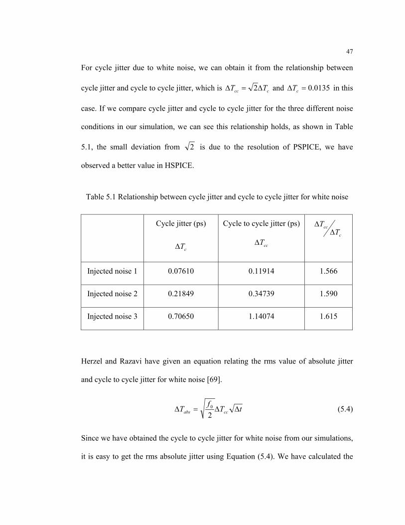
For cycle jitter due to white noise, we can obtain it from the relationship between
cycle jitter and cycle to cycle jitter, which is ccc TT ∆=∆ 2 and 0135.0=∆ cT in this
case. If we compare cycle jitter and cycle to cycle jitter for the three different noise
conditions in our simulation, we can see this relationship holds, as shown in Table
5.1, the small deviation from 2 is due to the resolution of PSPICE, we have
observed a better value in HSPICE.
Table 5.1 Relationship between cycle jitter and cycle to cycle jitter for white noise
Cycle jitter (ps)
cT∆
Cycle to cycle jitter (ps)
ccT∆c
ccT
T∆
∆
Injected noise 1 0.07610 0.11914 1.566
Injected noise 2 0.21849 0.34739 1.590
Injected noise 3 0.70650 1.14074 1.615
Herzel and Razavi have given an equation relating the rms value of absolute jitter
and cycle to cycle jitter for white noise [69].
tTf
T ccabs ∆∆=∆2
0 (5.4)
Since we have obtained the cycle to cycle jitter for white noise from our simulations,
it is easy to get the rms absolute jitter using Equation (5.4). We have calculated the

48
rms value of absolute jitter due to white noise for the three different noise conditions
and have compared these to the simulated absolute jitter, the simulated absolute jitter
should be very near the rms value and this trend is clearly shown in Fig.5.10.
In the above simulations, the frequency range for the injected noise is from 1Hz
to1GHz, since the oscillation frequency is 1.352GHz, only timing jitter from low
frequency noise due to an up conversion effect is involved in the simulations. In
reality, there is also timing jitter from high frequency noise due to down conversion.
We have extended the upper frequency limit to 20GHz, which is a typical cut off
frequency for CMOS technology, and have repeated the above simulation procedure
again. We get a cycle to cycle jitter of 0.0627ps for white noise. By using Equation
(5.4), we have calculated the rms value of absolute jitter due to device white noise,
as plotted in Fig. 5.11. Fig. 5.11 also shows the rms value calculated from an
analytical formula introduced by A.Hajimiri [71]
tTabs ∆=∆ κ (5.5)
char
DD
VV
PkT
⋅⋅=η
κ38 (5.6)
where η is 0.75 for single ended ring oscillators, P is total power dissipation, DDV
is the power supply voltage, charV is the characteristic voltage of the device, defined
as γVVchar
∆= for long channel devices, γ is 2/3 for long channel devices and
TDD VVV −=∆ )2( .

49
(a)
(b)
(c)
Figure 5.10 Comparison between simulated absolute jitter and calculated rms value(a) Injected noise 1(b) Injected noise 2(c) Injected noise 3

50
Figure 5.11 RMS absolute jitter versus time for white noise
From Fig.5.11, we can see at 1us, simulations predict a rms value of 1.63 ps, while
A. Hajimiri's analytical formula yields 2.746 ps. The difference comes from the fact
that there are some assumptions when deriving (5.6) in [71] such as TPTN VV = ,
which is not true in our case. Also the total channel noise given by Equation (18) in
[71], HzA /104472.1 223−× , is larger than our value obtained from analog
simulations of device noise, HzA /103438.5 224−× . A further check shows if we
project back to the noise value HzA /104472.1 223−× and then calculate the rms
absolute jitter at a 1us interval, we obtain 2.678ps, which is very close to the
analytical value 2.746ps obtained from A.Hajimiri's formula. A summary of the
above analysis is shown in Table 5.2.

51
Table 5.2 Comparison of simulation results and A. Hajimiri's analytical model for
RMS absolute jitter due to white noise at 1us
Simulated value Analytical value
1.63 ps (1)RMS absolute jitter at 1us
2.678 ps (2)
2.746 ps (2)
(1) Corresponding to when total channel noise is HzA /103438.5 224−× ,obtained from analog simulations of device noise.
(2) Corresponding to when total channel noise is HzA /104472.1 223−× , givenby Equation (18) in [71]. The RMS value of absolute jitter obtained fromsimulations matches that obtained from A.Hajimiri's formula.
Fig.5.11 predicts the jitter performance due to white noise in a ring oscillator. If it
were possible to derive a similar analytical relationship between rms absolute jitter
and cycle to cycle jitter for flicker noise, we could then easily predict the whole jitter
performance.
52
6. TIMING JITTER IN DIFFERENTIAL CMOS RING OSCILLATORS
6.1 Stationary Approach in Differential CMOS Ring Oscillators
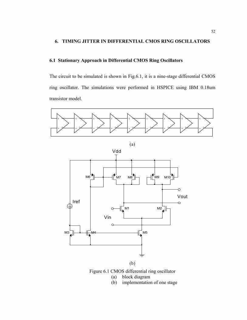
The circuit to be simulated is shown in Fig.6.1, it is a nine-stage differential CMOS
ring oscillator. The simulations were performed in HSPICE using IBM 0.18um
transistor model.
(a)
(b)
Figure 6.1 CMOS differential ring oscillator(a) block diagram(b) implementation of one stage
+
-
-+
+
-
-+
+
-
-+
+
-
-+
+
-
-+
+
-
-+
+
-
-+
+
-
-+
+
-
-+
IrefM2
M8 M9
Vdd
M3
Vin
M1
M10
M4 M5
M6 M7
Vout

53
As in the case of single ended CMOS ring oscillator, in differential one, the primary
concern is still to study the impact of device noise on timing jitter. The schematic for
the inverter cell is repeated in Fig. 6.2 (a) with noise source added, where 21ni , 2
2ni ,…,
210ni are the noise power spectral densities for transistors M1,…M10, these are the
intrinsic output referred noise sources for each transistor. In our simulations, we use
a common stationary approach to estimate the effects of all the noise sources
[51][71]. Since we take differential output, the effects of all internal noise sources in
the circuit can be replaced by an equivalent output referred noise source at one
output, as shown in Fig. 6.2 (b). The two noise sources at output means we will
inject and study 1/f noise and white noise separately. This equivalent noise power is
calculated at a fixed DC bias condition that corresponds to DC biasing point of the
oscillator. A linear circuit simulation is performed to get this noise power, as shown
in Fig. 6.2 (c).
The small-signal equivalent circuit of the inverter cell for AC noise analysis is shown
in Fig. 6.2 (d), where RL and CL represent the total resistance and capacitance at the
output node. Differential noise analysis should be used in this case since we will take
differential output. To determine the output, AC, differential voltage noise, the
circuit in Fig. 6.2 (d) should be replaced by the circuit in Fig. 6.2 (e). In this circuit,
the noise sources from each side are combined together, common mode noise
sources associated with the current mirrors, M3-M6, are cancelled by each other,
while differential ones added.
54
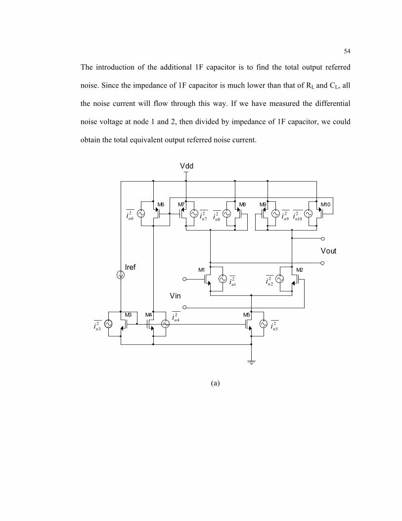
The introduction of the additional 1F capacitor is to find the total output referred
noise. Since the impedance of 1F capacitor is much lower than that of RL and CL, all
the noise current will flow through this way. If we have measured the differential
noise voltage at node 1 and 2, then divided by impedance of 1F capacitor, we could
obtain the total equivalent output referred noise current.
(a)
Vdd
Iref
Vin
M8
M2
Vout
M3
M9M6
M1
M5M4
M10M7
21ni
22ni
25ni
24ni
23ni
26ni 2
7ni 28ni
29ni
210ni

55
(b)
Figure 6.2 (Continued)
Vout
M4
Vdd
M7 M9
1/f noiseM1
IrefM2
M10M8
M3
M6
M5
Vin
White noise

56
(c)
26,5,4,3ni
21ni
22ni− 7ni 8ni 10ni 9ni
21ni−
22ni
26,5,4,3ni
(d)
Figure 6.2 (Continued)
M9
-
M1
M10
1F
M6
1F
M5
IrefM2
M8
M4
Vdd
Vdc
+
M3
M7
R
2
CLL
1 +
CL
-
1F R1F L
Vn
57
(e)
Figure 6.2 Illustration of stationary approach in differential CMOS Ring Oscillators(a) Differential inverter cell with noise sources(b) Equivalent output referred noise source(c) Circuit used to get the device noise power(d) Equivalent circuit for AC noise analysis(e) Simplified differential AC noise analysis circuit
6.2 Simulation of Timing Jitter in Differential CMOS Ring Oscillators, Resultsand Discussion
Simulation procedures are the same as single ended CMOS ring oscillator, so they
won’t be repeated here. Simulation results are shown in Fig. 6.3 to Fig. 6.5. Fig. 6.3
shows the absolute jitter versus time, Fig. 6.4 and Fig. 6.5 show cycle jitter and cycle
to cycle jitter versus time. The top part shows jitter due to flicker noise while lower
part shows jitter due to white noise. From Fig. 6.3 we can see the variation of
absolute jitter due to flicker noise has a dependence on the time, t , while for white
noise, it has a, 5.0t , dependence. These are consistent with accepted theory in the
literature [69-73]. Fig. 6.3 shows the measured rms value of absolute jitter due to
flicker noise [Provided by Teradyne Inc.], as we expect, the simulated absolute jitter
should be very near the rms value and this trend is clearly shown in Fig. 6.3 (a).
+
-
1F
21ni 2
2ni27ni
28ni 2
9ni210ni
RL CL 2nV

58
The cycle to cycle jitter we have obtained is 0.425 ps for flicker noise and 0.445 ps
for white noise. Cycle jitter due to white noise is 325.0=∆ cT ps, the relationship
between cycle jitter and cycle to cycle jitter due to white noise from simulations is
consistent with the analytical formula ccc TT ∆=∆ 2 , as shown in Table 6.1.
Table 6.1 Relationship between cycle jitter and cycle to cycle jitter for white noise
Cycle jitter (ps) cT∆ Cycle to cycle jitter (ps) ccT∆c
ccT
T∆
∆
0.325 0.445 1.369
Herzel and Razavi have given an equation relating the rms value of absolute jitter
and cycle to cycle jitter for white noise [69].
tTf
T ccabs ∆∆=∆2
0 (6.1)
Since we have obtained the cycle to cycle jitter for white noise from our simulations,
it is easy to get the rms absolute jitter using Equation (6.1). We have calculated the
rms value of absolute jitter due to white noise and have compared it to the simulated
absolute jitter, plotted in Fig.6.3 (b), as in the case of flicker noise, the simulated
absolute jitter varies but is near the rms value.
From the above analysis, the agreement between simulation and expected values all
serves to verify the validity of our technique.

59
(a)
(b)
Figure 6.3 Absolute jitter as a function of time(a) flicker noise(b) white noise

60
(a)
(b)
Figure 6.4 Cycle jitter as a function of time(a) flicker noise(b) white noise

61
(a)
(b)
Figure 6.5 Cycle to cycle jitter as a function of time(a) flicker noise(b) white noise

62
7. TIMING JITTER IN SILICON BJT /OR SIGE HBT ECL RINGOSCILLATORS
7.1 Stationary Approach in Silicon BJT /OR SiGe HBT ECL Ring Oscillators
We have employed the above methodology and investigated the timing jitter in
silicon BJT /or SiGe HBT ECL ring oscillators. The circuit diagram is shown in
Fig.7.1. It is a nine stage silicon BJT/or SiGe HBT ECL ring oscillator with Vdd=3 V
[48][74][75]. The simulations were performed in HSPICE using a simple generic
transistor model with a unity current gain frequency of 16 GHz and an IBM SiGe
HBT transistor model respectively.
As in the case of the CMOS differential ring oscillator, in a silicon BJT/or SiGe HBT
ECL ring oscillator, we use a common stationary approach to estimate the effects of
all the noise sources. An equivalent output referred noise source is used to represent
the effects of all internal noise sources in the circuit. Fig.7.2 shows an illustration of
the total equivalent output noise power for one stage. The total equivalent output
noise power for one stage of the silicon BJT and SiGe HBT oscillators are obtained
from an analog noise SPICE simulation at output of one stage and calculated at a
fixed DC bias condition when the stage is half way through a transition, as shown in
Fig. 7.3.
Since in the silicon BJT transistor model, the default flicker noise coefficient KF is
set to zero, we use the following method to obtain the PSD of flicker noise. The
flicker noise is modeled by setting the total equivalent output noise corner frequency

63
fc to be 40kHz after the white noise has already been obtained from the circuit in
Fig.7.3. Such a low l/f noise corner frequency, or even lower corner frequency, is
commonly observed on small silicon bipolar transistor devices. In the SiGe HBT
transistor model, flicker noise is calculated by the IBM default flicker noise
coefficient KF.
(a)
(b)
Figure 7.1 Nine stage silicon BJT/or SiGe HBT ECL ring oscillator(a) block diagram(b) implementation of one stage
+
-
-+
+
-
-+
+
-
-+
+
-
-+
+
-
-+
+
-
-+
+
-
-+
+
-
-+
+
-
-+
Q1
R1
Vdd
Q3
R4
Vout- Vin+
R3
Vout+
Q4
Q2
R5
Vin-
R2
64
Figure 7.2 Illustration of output noise power for one stage of a silicon BJT/or SiGeHBT ring oscillator
Figure 7.3 Circuit used to get the device noise power for silicon BJT/or SiGe HBTECL ring oscillator
fCinf =2
whitenw Ci =2
1 fc
2ni (A 2 /Hz)
f (Hz)
Q3
R5R1Vdc
R41F
Vdd
R3
1F
R2
Q2Q1
Q4

65
7.2 Simulation of Timing Jitter in Silicon BJT /OR SiGe HBT ECL RingOscillators, Results and Discussion
Simulation procedures are the same as CMOS differential ones, so they won’t be
repeated here. Fig. 7.4 shows the histograms of silicon BJT ECL ring oscillator clock
periods for the noise free case, and the noise-injected case, SiGe HBT cases are
similar but not shown here. Part (a) for the noise free case shows most of the clock
periods being near a single value. Part (b) shows the variations in clock periods with
white noise while Part (c) shows the variations in clock periods with flicker noise.
These distributions in clock periods represent clock jitter.
Fig. 7.5 shows the absolute jitter as a function of time for silicon BJT ring oscillator
due to flicker noise. Simulation shows a jitter of 6ps for flicker noise after a 1us
interval.
Fig. 7.6 shows the absolute jitter as a function of time for a SiGe HBT ECL ring
oscillator due to flicker noise. Simulation shows a jitter of 144ps for flicker noise
after a 1us interval.
For a free running oscillator, cycle jitter and cycle to cycle jitter are often used,
however in some cases, we are more concerned with absolute jitter. We have
compared the simulation results of absolute jitter for CMOS, silicon BJT and SiGe
HBT ring oscillators. The results are shown in Table 7.1. From Table 7.1, we can
see, compared to a CMOS ring oscillator, the silicon BJT ring oscillator has a much
lower jitter while these two oscillators have a similar oscillation frequency. For the

66
(a)
(b)
(c)
Figure 7.4 Histogram of silicon BJT ECL ring oscillator clock periods(a) for noise free case(b) for white noise-injected case(c) for flicker noise-injected case

67
SiGe HBT ring oscillator, the absolute jitter is close to that of the CMOS one,
however, we should note that the oscillation frequency of the SiGe HBT ring
oscillator is much higher than that of the CMOS one, at the same time interval it has
more clock periods. Since absolute jitter is an accumulated effect, the more clock
periods, the more jitter which will accumulate. If we make a comparison at the same
number of clock periods, we should expect a lower jitter for the SiGe HBT ring
oscillator. Thus silicon BJT and/or SiGe HBT ring oscillators are a potential choice
for low jitter applications.
Figure 7.5 Absolute jitter as a function of time for silicon BJT ECL ring oscillatordue to flicker noise

68
Figure 7.6 Absolute jitter as a function of time for SiGe HBT ECL ring oscillator dueto flicker noise
Table 7.1 Absolute jitter due to flicker noise at 1us for three different types of oscillator
Oscillator type Absolute Jitter (ps) Oscillation Frequency (MHz)
CMOS 152 772
Silicon BJT 6 626
SiGe HBT 144 2271

69
8. CONCLUSION
In the first part of this dissertation work, we have demonstrated from theory and
experiment that 1/f noise in bipolar transistors, with a low impedance in the base circuit,
has a strong dependence on collector-emitter voltage and power dissipation at
frequencies in the kHz range. A detailed comparison between the theory and the 1/f
noise measured on bipolar transistors has been given in this dissertation work. It can be
seen our theory fits the experimental data at the higher frequencies. At low frequency
1Hz and below, further work needs to be done to refine the model. However, noise at
such low frequencies is not relevant to phase noise in communication systems. These
new results are particularly relevant to phase noise in voltage-controlled oscillators
and the engineering choice of whether to use CMOS or bipolar technology in
wireless communication systems.
Interestingly enough temperature fluctuations might well describe some of the low
frequency noise observed in vacuum tube devices and for which there never was any
completely satisfactory explanation.
In the second part of this dissertation work, we have developed a large signal transient
simulation technique to simulate phase noise due to device noise in a 2G Hz BJT LC
oscillator. Flicker and white noise are simulated as a sum of sine waves with
different amplitudes and random phase in MATLAB, which has a 1/f or white
characteristics after FFT, then injecting into LC BJT oscillator and upconvert into
phase noise. The simulation results are consistent with the empirical theory that the

70
phase noise resulting from direct upconvertion of flicker noise has a 1/f3 and white
noise has a 1/f2 dependence on offset frequency. It is also shown that phase noise at
4.7 MHz offset from flicker noise is -150.7 dBC/Hz and from white noise is –132
dBc/Hz. At this point it is white noise dominated. The simulation result is in good
agreement with the experimental value of –136 dBc/Hz at this offset frequency
reported in the literature by Zannoth and Kolb [56], our simulation is able to predict
phase noise correctly. The development of such technique to simulate phase noise in
the oscillator will be very helpful in designing low phase noise oscillators.
In the third part of this dissertation work, we have developed a time-domain method to
simulate timing jitter due to device noise and have applied it to a three stage single-
ended and a nine-stage differential ring oscillator. An equivalent output referred
noise source is used to represent the effect of all internal noise sources in the circuit.
Flicker and white noise, which is simulated as a sum of sine waves with random
phase by using MATLAB, is then modeled as the equivalent output referred noise
and injected into the output of each stage as a PSPICE/HSPICE piecewise linear
waveform. A time domain transient analysis is then performed and output data is
analyzed by MATLAB to calculate the timing jitter. Simulation results show the
variation of absolute jitter due to flicker noise has a, t , dependence, while for white
noise, it has a, 5.0t , dependence. These are consistent with accepted theory. Two
important parameters cycle jitter and cycle to cycle jitter used to describe jitter
performance can be obtained from the simulations. A comparison between simulated
data and an analytical formula is also given in this dissertation work, and it shows

71
that the simulated absolute jitter is near the rms value predicted by an analytical
formula. The relationship between cycle jitter and cycle to cycle jitter due to white
noise from simulations is consistent with the analytical formula. The rms value of
absolute jitter due to white noise obtained from simulations matches that obtained
from A.Hajimiri's formula. Simulation results are also compared with measurement
results, it is shown that simulation results are very close to measurement results. All
these serve to verify the validity of this technique.
There have been some analytical techniques to predict jitter [69-73], unfortunately,
however, the analytical techniques have been developed only for white noise and not
1/f noise. The absolute jitter due to 1/f noise is usually more important since it
increases linearly with time [71]. We have demonstrated here a technique to simulate
the absolute jitter due to 1/f noise.
We have employed this methodology and investigated timing jitter in silicon BJT
and SiGe HBT ECL ring oscillators. We have shown silicon BJT and SiGe HBT
oscillators have lower jitter compared to their CMOS counterparts. As such silicon
BJT and/or SiGe HBT ring oscillators are a potential choice for low jitter
applications. Silicon BJT and/or SiGe HBT’s have much lower l/f noise corner
frequencies [76,77] than CMOS devices.
The method described in this dissertation is also applicable to other types of
oscillators such as LC oscillators, as well as other kinds of noise source as power
supply and substrate noise. The ability to predict the impact of timing jitter in
electronic circuits via simulation is useful in designing low jitter circuits [78].

72
Bibliography
1. A. L. McWhorter, “1/f noise and germanium surface properties,” SemiconductorSurface Physics, R.H. Kingston, Ed., Philadelphia, PA: Univ. of PennsylvaniaPress, pp. 207-228, 1957.
2. Leopoldo D. Yau and Chih-Tang Sah, “Theory and experiments of low-frequency Generation-recombination noise in MOS transistors,” IEEE Transactions on Electron Devices, vol. ED-16, no. 2, Feb. 1969.
3. F. N. Hooge, “1/f noise is no surface effect,” Phys. Lett., vol. A-29, pp. 139-140, 1969.
4. L. K. J. Vandamme, “Model for 1/f noise in MOS transistors biased in the linearregion,” Solid-State Electronics, vol. 23, pp. 317-323, 1980.
5. L. K. J. Vandamme and H. M. M. Werd, “1/f noise model for MOSTs biased innonohmic region,” Solid-State Electronics, vol. 23, pp. 325-329, 1980.
6. H. S. Park, A. Van Der Ziel and S. T. Liu, “Comparison of two 1/f noise modelsin MOSFET’s,” Solid-State Electronics, vol. 25, no. 3, pp. 213-217, 1982.
7. Hiroaki Mikoshiba, “1/f noise in n-channel silicon-gate MOS transistors,” IEEETransactions on Electron Devices, vol. ED-29, no. 6, June 1982.
8. G. Reimbold, “Modified 1/f trapping noise theory and experiments in MOStransistors biased from weak to strong inversion-influence of interface states,”IEEE Transactions on Electron Devices, vol. ED-31, no. 9, pp.1190-1198, Sept.1984.
9. G. Nicollini, D. Pancini and S. Pernici, “Simulation-oriented noise model forMOS devices,” IEEE Journal of Solid-State Circuits, vol. SC-22, no. 6, pp.1209-1212, Dec. 1987.
10. A.van der Ziel, “Unified presentation of 1/f noise in electronicdevices: fundamental 1/f noise sources,” Proc. IEEE, vol. 76, no. 3, pp. 233-258, March 1988.
11. K. K. Hung and P. K. Ko, “A unified model for the flicker noise in metal-oxidesemiconductor field-effect transistors,” IEEE Transactions on Electron Devices,vol. 37, no. 3, pp. 654-664, March 1990.

73
12. Kwok K. Hung, Ping K. Ko, Chenming Hu and Yiu C. Cheng, “A physics-basedMOSFET noise model for circuit simulators,” IEEE Transactions on ElectronDevices, vol. 37, no. 5, May 1990.
13. T.Elewa and B. Boukriss, “Low-frequency noise in depletion-mode DIMOXMOS Transistors,” IEEE Transactions on Electron Devices, vol. 38, no. 2, pp.323-327, Feb. 1991.
14. J. T. Hsu and J. Wang, “Flicker noise in thin film depleted SOI MOSFETS,”IEEE Device Research Conference, pp. 30-31, 1991.
15. Daniel M. Fleetwood, “Border traps in MOS devices,” IEEE Transactions onNuclear Science, vol. 39, no. 2, April 1992.
16. Munecazu Tacano, “Hooge fluctuation parameter of semiconductormicrostructures,” IEEE Transactions on Electron Devices, vol. 40, no. 11, Nov.1993.
17. C. H. Cheng and C. Surya, “The effect of hot-electron injection on the propertiesof flicker noise in n-channel MOSFET’s,” Solid-State Electronics, vol. 36, no.3, pp. 475-479, 1993.
18. D. M. Fleetwood and P. S. Winokur, “Effects of oxide traps, interface traps, andborder traps on metal-oxide-semiconductor devices,” J. Appl. Phys, vol. 73,no.10, pp. 5058-5072, May 15, 1993.
19. M. Tsai and T. Ma, “1/f noise in hot-carrier damaged MOSFET’s: effects ofoxide charge and interface traps,” IEEE Electron Device Letters, vol. 14, no. 5,May 1993.
20. John H. Scofield, Nick Borland, and Daniel M. Fleetwood, “Reconciliation ofdifferent gate-voltage dependencies of 1/f noise in n-MOS and p-MOStransistors,” IEEE Transactions on Electron Devices, vol. 41, no. 11, pp. 1946-1952, Nov. 1994.
21. J. Chang, A. A. Abidi and C. R. Viswanathan, “Flicker noise in CMOStransistors from subthreshold to strong inversion at various temperatures,” IEEETrans. on Electron Devices, vol. 41, no. 11, pp. 1965-1971, Nov. 1994.
22. F. N. Hooge, “1/f noise sources,” IEEE Transactions on Electron Devices, vol.41, no. 11, Nov. 1994.
23. L. K. J. Vandamme, X. Li and D. Rigaud, “1/f noise in MOS devices, mobilityor number fluctuations,” IEEE Trans. on Electron Devices, vol. 41, no. 11, pp.1936-1944, Nov. 1994.

74
24. E. Simoen and C. Claeys, “Correlation between the low-frequency noise spectraldensity and the static device parameters of silicon-on-insulator MOSFET’s,”IEEE Trans. on Electron Devices, vol. 42, no. 8, pp. 1467-1472, Aug. 1995.
25. M. Aoki and M. Kato, “Hole-induced 1/f noise increase in MOS transistors,”IEEE Electron Device Letters, vol. 17, no. 3, pp. 118-120, March 1996.
26. N. Lukyanchikova, M. Petrichuk, N. Garbar, E. Simoen and C. Claeys, “Backand front interface related generation-recombination noise in buried-channel SOIp-MOSFET's,” IEEE Transactions on Electron Devices, vol. 43, no. 3, pp. 417-423, March 1996.
27. C. Hu, G. P. Li, E. Worley and J. White, “Consideration of low-frequency noisein MOSFET's for analog performance,” IEEE Electron Device Letts., vol. 17,no. 12, pp. 552-554, Dec. 1996.
28. P. Morfouli, G. Ghibaudo, T. Ouisse, E. Bogel, W. Hill, B. Misra, P. McLartyandJ. J. Wortman, “Low-frequency noise characterization of n- and p-MOSFET’swith ultrathin oxynitride films,” IEEE Electron Device Letters, vol 17, no. 8,Aug. 1996.
29. J. A. Babcock, C. E. Gill, J. M. Ford, D. Ngo, E. Spears, J. Ma, H. Liang, D. J.Spooner and S. Cheng, “1/f noise in graded-channel MOSFET's for low-powerlow-cost RFIC's,” Abst. IEEE Device Research Conf., Fort Collins, pp. 122-123,1997.
30. T. Boutchacha, G. Ghibando, G. Guegan and T. Skotnicki, “Low frequencynoise characterization of 0.18um Si CMOS transistors,” Microelectron Reliab.,vol. 37, no. 10/11, pp. 1599-1602, 1997.
31. C. Jakobson, I. Bloom and Y. Nemirovsky, “1/f noise in CMOS transistors foranalog applications from subthreshold to saturation,” Solid-State Electronics, vol.42, no. 10, pp. 1807-1817, 1998.
32. D. R. Wolters and A. T. A. Zegers-van Duijnhove, “Modeling 1/f noise ofelectronic devices,” Proceedings of the 1997 14th International Conferenceon Noise in Physical Systems and 1/f Fluctuations, pp. 471-477, July 14-18,1997.
33. M. B. Das, “On the current dependence of low-frequency noise in bipolartransistors,” IEEE Transactions on Electron Devices, vol. 22, no. 12, pp. 1092-1098, Dec. 1975.

75
34. M. Conti. “Surface and bulk effects in low frequency noise in NPN planartransistors,” Solid-State Electronics, vol. 13, no. 11, pp. 1461-1469, 1970.
35. R. C. Jaeger and A. J. Brodersen, “Low frequency noise sources in bipolarjunction transistors,” IEEE Transactions on Electron Devices, vol. 17, no. 2, pp.128-134, Feb. 1970.
36. K. F. Knott, “Experimental location of the surface and bulk 1/f noise currents inlow-noise high-gain n-p-n planar transistors,” Solid-State Electronics, vol. 16,no. 12, pp. 1429-1434, 1973.
37. M. Stoisiek and D. Wolf, “Origin of 1/f noise in bipolar transistors,” IEEETransactions on Electron Devices, vol. 27, no. 9, pp. 1753-1757, Sep. 1980.
38. A. H. Pawlikiewicz, A. Van der Ziel, G. S. Kousik, and C. M. van Vliet,“Fundamental 1/f noise in silicon bipolar transistors,” Solid-State Electronics,vol. 31, no. 5, pp. 831-834, 1988.
39. T. G. M. Kleinpenning, “Location of low frequency noise sources insubmicrometer bipolar transistors,” IEEE Transactions on Electron Devices, vol.39, no. 6, pp. 1501-1506, June 1992.
40. S. L. Jang, “Formulation of mobility fluctuation 1/f noise in bipolar transistors,”Solid-State Electronics, vol. 36, no. 11, pp. 1541-1545, 1993.
41. J. Kilmer, A. van der Ziel, and G.Bosman, “Presence of mobility fluctuation 1/fnoise identified in silicon p+-n-p transistors,” Solid-State Electronics, vol. 26, no.1, pp. 71-74, 1983.
42. A. H. Pawlikiewicz, and A. Van der Ziel, “Location of 1/f noise sources in BJTs-II. Experiment,” IEEE Transactions on Electron Devices, vol. 34, no. 9, pp.2009-2012, Sep. 1987.
43. J. L. Plumb and E. R. Chenette, “Flicker noise in transistors,” IEEE Trans. onElectron Devices, vol. ED-10, pp. 304-308, Sept. 1963.
44. M. Jamal Deen, S. Rumyantsev, R. Bashir and R. Taylor, “Measurements andcomparison of low frequency noise in npn and pnp polysilicon emitter bipolarjunction transistors,” Journal of Applied Physics, vol. 84, pp. 625-633, July 1998.
45. L. Forbes, “1/f noise due to temperature fluctuations in heat condition,” in IEEEDevice Research Conference, Santa Barbara, June 1996, pp. 46-47.

76
46. L. Forbes, M .S. Choi and W. Cao, “1/f noise due to temperature fluctuations inheat conduction in bipolar transistors,” Microelectronics Reliability, vol. 39,pp.1357- 1364, Sept. 1999.
47. C. Kittel and H. Kroemer, Thermal Physics, 2nd Ed., New York: Freeman, 1980,
p. 424.
48. P. R. Gray and R. G. Meyer, “Analysis and Design of Analog Integrated Circuits,” Third edition, John Wiley & Sons, Inc., 1993.
49. D. B. Leeson, “A simple model of feedback oscillator noise”, Proceedings of theIEEE, pp. 329-330, Feb. 1966.
50. B. Razavi, “A study of phase noise in CMOS oscillators”, IEEE J. Solid-StateCircuits, vol. 31, no. 3, pp. 331-343, March 1996.
51. A. Hajimiri and T. H. Lee, “A general theory of phase noise in electricaloscillators”, IEEE J. Solid-State Circuits, vol. 33, no. 2, pp. 179-194, February1998.
52. A. Hajimiri and T. H. Lee, “Phase noise in CMOS differential LC oscillators”,Digest of technial papers of the Symp. On VLSI Circuits, pp. 48-51, 1998.
53. Mini-Circuits, “VCO Phase noise”, http://www.minicircuits.com/appnote/vco15-6.htm, Mini Circuits, 13 Neptune Avenue, Brooklyn, NY 11235, 1997-1998.
54. D. Xie and L. Forbes, “Phase noise on a 2-GHz CMOS LC Oscillator,”IEEE Trans. on Computer-Aided Design of Integrated Circuits and Systems,vol.19, pp. 773-778, July 2000
55. L. Forbes, M. Cheng and J. Zhou, “Simulation of phase noise generated by whitenoise in a 1.7-GHz CMOS LC Oscillator,” IEE Electronics Letters,. vol.36, pp.1909-1911, 2000
56. M. Zannoth, and B. Kolb, “Fully integrated VCO at 2 GHz,” IEEE Journal ofSolid-State Circuits , vol. 33, no. 12, pp. 1987-1991, Dec.1998.

77
57. Adler, Joseph V., “Clock-source jitter: A clear understanding aids oscillatorselection,” Electronics Design News Magazine, vol.44, no.4, Feb.1999
58. Beomsup Kim, Todd C.Weigandt , and Paul R.Gray, “ PLL/DLL system noiseanalysis for low jitter clock synthesizer design,” Proceedings of the 1994 IEEEInternational Symposium on Circuits and Systems, vol.4, pp. 31-34, June, 1994
59. Lin Wu and William C.Black Jr., “A low jitter 1.25 GHz CMOS analog PLL forclock recovery,” Proceedings of the 1998 IEEE International Symposium onCircuits and Systems, vol.1, pp. 167-170, June, 1998
60. Chang-Hyeon Lee, Jack Cornish, Kelly McClellan, and John Choma,Jr., “Designof Low Jitter PLL for clock generator with supply noise insensitive VCO,”Proceedings of the 1998 IEEE International Symposium on Circuits and Systems,vol.1, pp. 233-236, June, 1998
61. David W.Boerstler, “A low jitter PLL clock generator for microprocessors withlock range of 340-612 MHz,” IEEE J. Solid-State Circuits, vol.34, pp.513-519,April 1999
62. Vincent R.von Kaenel, “A high-speed, low-power clock generator for amicroprocessor application, ” IEEE J. Solid-State Circuits, vol.33, pp.1634-1639,Nov. 1998
63. Johan Schoukens, Frank Louage, and Yves Rolain, “ Study of the influence ofclock instabilities in synchronized data acquisition systems,” IEEE Transactionson Instrumentation and Measurement, vol.45, no.2, pp. 601-604, April 1996
64. S.Merchan, A.Garcia Armada and J.L.Garcia, “ Performance of digital collectiveantenna systems in the presence of phase noise and clock jitter,” IEEETransactions on Consumer Electronics, vol.43, no.2, pp. 188-196, May 1997
65. Selim Saad Awad, “ The effects of accumulated timing jitter on some sine wavemeasurements,” IEEE Transactions on Instrumentation and Measurement,vol.44, no.5, pp 945-951, October 1995

78
66. Huawen Jin and Edward K.F.Lee, “A digital technique for reducing clock jittereffects in time-interleaved A/D converter,” Proceedings of the 1999 IEEEInternational Symposium on Circuits and Systems, vol.2, pp. 330-333, June, 1999
67. Michael K.Williams, “A discussion of methods for measuring low-amplitudejitter,” Proceedings of IEEE International Test Conference pp 646-652 Oct.1995
68. Sevalia, Piyush, “Straightforward techniques cut jitter in PLL-based clockdrivers,” Electronics Design News Magazine, vol.40, no.24, Nov.1995
69. Frank Herzel and Behzad Razavi, “A study of oscillator jitter due to supply andsubstrate noise,” IEEE Transactions on Circuits and Systems-II: Analog andDigital Signal Processing, vol.46, no.1, pp 56-62, Jan. 1999
70. Todd C.Weigandt, Beomsup Kim, and Paul R.Gray, “Analysis of timing jitter inCMOS Ring Oscillators,” Proceedings of the 1994 IEEE InternationalSymposium on Circuits and Systems, vol.4, pp. 27-30, June, 1994
71. Ali Hajimiri, Sotirios Limotyrakis, and Thomas H.Lee, “Jitter and Phase noise inring oscillators,” IEEE J. Solid-State Circuits, vol.34, pp.790-804, June 1999
72. J.McNeill, “Jitter in ring oscillators,” IEEE J. Solid-State Circuits, vol.32,pp.870-879, June 1997
73. David C. Lee, “Modeling of Timing Jitter in Oscillators,”http://www.mentor.com/dsm/tpapers.cfm
74. David A. Johns and Ken Martin, “Analog Integrated Circuit Design,” John Wiley& Sons, NY, 1997
75. Behzad Razavi, Yusuke Ota, Robert G. Swartz, “Design Techniques for Low-Voltage High-Speed Digital Bipolar Circuits,” IEEE J. Solid-State Circuits,vol.29, no.3, pp. 332-339, March 1994
76. S. Bruce, K.J. Vandamme, and A. Rydberg, “Temperature dependence andelectrical properties of dominant low-frequency noise source in SiGe HBT,”IEEE Trans. on Electron Devices, vol. 47, no. 5, pp. 1107-1112, May 2000.

79
77. G. Niu, J.D. Cressler, Z. Jin and S. Zhang, “Transistor noise in SiGe HBTtechnology,” Proc. IEEE Bipolar Circuits and Technology Meeting,Minneapolis, MN, June 2000, pp. 207-210.
78. L. Forbes and C.W. Zhang (Invited), “1/f noise and clock jitter in digitalelectronic systems fluctuations,” 1st Int. Symp. On Fluctuations and Noise, SantaFe, NM, 1-4 June 2003.
79. Application note, “Jitter Test Results in Programmable Oscillators,”
http://www.viteonline.com/appnotes/JitterVP.pdf

80
APPENDICES

81
Appendix A: Device Noise Measurement
Two kinds of approaches are used to determine the device noise. One is an
automated measurement, Fig. A.1. shows the schematic of the automated noise
measurement system for NPN bipolar transistor. In order to reduce any power supply
noise effect at the collector node, the NPN transistor is connected upside down with
negative power supplies to its base and emitter.
Figure A.1 Automated Noise Measurement System

82
The other one, ADC board based measurement system has been developed for
measurement at higher frequencies. Fig. A.2. shows the schematic of such
measurement system. The transistor setup is the same as that in the automated setup.
Figure A.2 ADC Board Based Noise Measurement System

83
The measured time domain noise data is post processed by a MATLAB program.
The results are plotted in frequency domain.
% PSD of npn bjt 1/f noise% data is taken from lab
clear all; close all
item = 'Measured NPN BJT current noise';load 'pn2222a3.dat' %BJT 100000 dataVout = pn2222a3;%Vref = ; %balance voltage supply --need to change each datadate = '5/16/00'; %the date when data is takenfs=26; %sampling rate of DMMgain=90; %noise amplification by LM741Rload=100; %load resistorVnoise = Vout./gain;%Vnoise = (Vref - Vout)./gain; %unit= VInoise = ( Vnoise./Rload); %unit= AL = length(Inoise); % L is also a window size. As L get larger magnitude of FFT% gets closer to theoretical value
%SETUP AXISf = fs .* ( 0:1/L:1-1/L ); % up to f=fsf = f(1:L/2); % up to fs/2time=(0:L-1)/fs;
%PSD of NOISEmag = (1/(L*fs))*abs( fft(Inoise) ).^2; %unit= A^2/Hzmag = mag(1:L/2);
figure(1);subplot(2,1,1);
plot(time,Inoise); grid on;%axis([0.1,100,1e-22,1e-8]);%title(sprintf('%s (%d pts, %s)',item,L,date));xlabel('Time (S)');ylabel('Magnitude (A)');zoom on
subplot(2,1,2);loglog(f,mag,'r'), hold on, grid

84
%axis([0.1,100,1e-22,1e-8]);title('PSD of NPN BJT PN2222A Noise RL=100.0 ohm Vee=11.2V
Ic=10mA');%title('PSD of Collector Current Noise (Rl=100 ohm)');xlabel('Frequency (Hz)'); ylabel('PSD of collector current noise (A^2/Hz)');
hold on, loglog(f,1e-17./f.^2,'k') hold on, loglog(f,1e-17./f.^1,'b-.'), zoom on hold off

85
Appendix B: MATLAB Program for Modeling of Random Phase Flicker Noiseand White Noise
I. Random-Phase Flicker Noise Simulation by Matlab ( File name:cmosfjll.m)
clear all; close all
AF=1; % known constantCF=5.82286e-14; % assumed CF value
% frequency changes from 1Hz to 10 GHz in logspace
f=logspace(0,10,1000);nf=length(f);deltaf=diff(f);f(:,nf)=[ ];
rand('state',sum(100*clock)); % rand function in MATLAB
x=rand(length(f),1);
% HSPICE Level 2&3 1/f noise in NMOSflicker=CF./(f.^AF); % unit=A^2/HzInd=flicker.^0.5; % unit=A/Hz^0.5
% amplitude of drain current noiseIamp=Ind.*deltaf.^(1/2); % unit=A
% Save data into files for MS EXCEL usef1=f'; flicker1=flicker'; Iamp1=Iamp';outputdata1=[f1 flicker1]; outputdata2=[f1 Iamp1];save figure1.dat outputdata1 -asciisave figure2.dat outputdata2 -ascii
figure(1)subplot(2,2,1)loglog(f,flicker,'-*'); grid on;%title('Modeling flicker noise with KF= ');xlabel('Frequency (Hz)');ylabel('Flicker noise (A^2/Hz)'); zoom on

86
subplot(2,2,2)loglog(f,Iamp,'*'); grid on;axis([1e0,1e9,1e-7, 1e-5]);%title('Calculated amplitude of sine waves with KF= ');xlabel('Frequency (Hz)');ylabel('Amplitude of sine waves (A)');
zoom on
n=100;tstart=0;tstop=0.5e-6;outputdata3=[ ];
for i=1:n
% total MATLAB simulation time with 100ps sampling delay% total simulation time needs to be larger than the final Tstop Value in the transient% analysis
t=tstart:1e-10:tstop;
%for i=1:length(f)% x=rand(1);% sum1(i,:)=Iamp(i)*sin(2*pi*f(i)*t+2*pi*x);%end% sum2=sum(sum1);
Imat=repmat(Iamp',1,length(t));fmat=repmat(f',1,length(t));tmat=repmat(t,length(f),1);
xmat=repmat(x,1,length(t));
sum1=Imat.*sin(2*pi*fmat.*tmat+2*pi*xmat);
sum2=sum(sum1);
t1=t'; sum3=sum2';noise1=[t1 sum3];noise2=[outputdata3;noise1];outputdata3=noise2;
clear t t1 *mat sum* noise*;
tstart=tstop+1e-10;

87
tstop=tstop+0.5e-6;
end
% Save data into file for HSPICE simulation and EXCEL use
save figure3.dat outputdata3 -ascii
% 1/f noise with random phase% data is taken from Matlab simulationload 'figure3.dat' time=figure3(:,1);noise=figure3(:,2);
subplot(2,2,3)plot(time*1e6,noise*1e6); grid on;xlabel('Time (us)');ylabel('Sum of Sine waves with random phase (uA)');%title('Sum of sine waves with random phase with KF= ');
fs=1e10; % sampling frequency
L=32768; % L is also a window size. As L get larger magnitude of FFT gets closer% to theoretical value
%SETUP AXISf1 = fs.* ( 0:1/L:1-1/L ); % up to f=fsa = L/2;a = round(a);f = f1(2:a); % up to fs/2
mag = fft(noise,L); % L is the size of windows
% Power Spectral Density (PSD)power = mag.* conj(mag) /(fs* L);power = power(2:a);subplot(2,2,4);
loglog(f,power,'*')axis([0,1e9,1e-24, 1e-14]);grid on;%title('Power spectral density of the sum of sine waves with random phase');xlabel('Frequency (Hz)');ylabel('PSD of the Sum (A^2/Hz)');hold on;
loglog(f,1e-10./f.^1,'k'), text(1e6, 2e-16, '1/f');
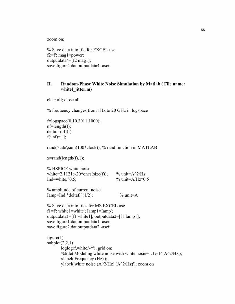
88
zoom on;
% Save data into file for EXCEL usef2=f'; mag1=power;outputdata4=[f2 mag1];save figure4.dat outputdata4 -ascii
II. Random-Phase White Noise Simulation by Matlab ( File name:whitel_jitter.m)
clear all; close all
% frequency changes from 1Hz to 20 GHz in logspace
f=logspace(0,10.3011,1000);nf=length(f);deltaf=diff(f);f(:,nf)=[ ];
rand('state',sum(100*clock)); % rand function in MATLAB
x=rand(length(f),1);
% HSPICE white noisewhite=2.1121e-20*ones(size(f)); % unit=A^2/HzInd=white.^0.5; % unit=A/Hz^0.5
% amplitude of current noiseIamp=Ind.*deltaf.^(1/2); % unit=A
% Save data into files for MS EXCEL usef1=f'; white1=white'; Iamp1=Iamp';outputdata1=[f1 white1]; outputdata2=[f1 Iamp1];save figure1.dat outputdata1 -asciisave figure2.dat outputdata2 -ascii
figure(1)subplot(2,2,1) loglog(f,white,'-*'); grid on;
%title('Modeling white noise with white nosie=1.1e-14 A^2/Hz');xlabel('Frequency (Hz)');ylabel('white noise (A^2/Hz) (A^2/Hz)'); zoom on

89
subplot(2,2,2)loglog(f,Iamp,'*'); grid on;%axis([1e0,1e9,1e-8, 1e-6]);%title('Amplitude of sine waves when white nosie=1.1e-14 A^2/Hz');xlabel('Frequency (Hz)');ylabel('Amplitude of sine waves (A)');
zoom on
n=100;tstart=0;tstop=0.5e-6;outputdata3=[ ];
for i=1:n
% total MATLAB simulation time with 100ps sampling delay% total simulation time needs to be larger than the final Tstop Value in the transient% analysis
t=tstart:1e-10:tstop;
%for i=1:length(f)% x=rand(1);% sum1(i,:)=Iamp(i)*sin(2*pi*f(i)*t+2*pi*x);%end% sum2=sum(sum1);
Imat=repmat(Iamp',1,length(t));fmat=repmat(f',1,length(t));tmat=repmat(t,length(f),1);
xmat=repmat(x,1,length(t));
sum1=Imat.*sin(2*pi*fmat.*tmat+2*pi*xmat);
sum2=sum(sum1);
t1=t'; sum3=sum2';noise1=[t1 sum3];noise2=[outputdata3;noise1];outputdata3=noise2;
clear t t1 *mat sum* noise*;
tstart=tstop+1e-10;

90
tstop=tstop+0.5e-6;
end
% Save data into file for HSPICE simulation and EXCEL use
save figure3.dat outputdata3 -ascii
% white noise with random phase% data is taken from Matlab simulation
load 'figure3.dat' time=figure3(:,1);noise=figure3(:,2);
subplot(2,2,3)plot(time*1e6,noise*1e6); grid on;xlabel('Time (us)');ylabel('Sum of Sine waves with random phase (uA)');%title('Sum of sine waves with random phase');
fs=1e10; % sampling frequency
L=32768; % L is also a window size. As L get larger magnitude of FFT gets closer% to theoretical value
%SETUP AXISf1 = fs.* ( 0:1/L:1-1/L ); % up to f=fsa = L/2;a = round(a);f = f1(2:a); % up to fs/2
mag = fft(noise,L); % L is the size of windows
% Power Spectral Density (PSD)power = mag.* conj(mag) /(fs* L);power = power(2:a);subplot(2,2,4);
loglog(f,power,'*')%axis([0,1e9,1e-24, 1e-16]);grid on;%title('Power spectral density of the sum of sine waves with random phase');xlabel('Frequency (Hz)');ylabel('PSD of the Sum (A^2/Hz)');hold on;

91
zoom on;
% Save data into file for EXCEL usef2=f'; mag1=power;outputdata4=[f2 mag1];save figure4.dat outputdata4 -ascii

92
Appendix C: Procedure of Phase Noise Simulation in Oscillators
I. Noise data creation
Create noise data by using cmosfjll.m (for flicker noise) and whitel_jitter.m (for
white noise) if PSD of flicker noise and white noise is given
II. HSPICE PWL Noise source
Write noise data into HSPICE PWL format, named as for example flicker.dat.
Here is an example.
* Injection of 1/f noise
Inoise 9 4 pwl(0.0000000e+00 5.4859467e-07+ 1.0000000e-10 7.2983248e-07+ 2.0000000e-10 8.6251607e-07+ 3.0000000e-10 9.6382932e-07+ 4.0000000e-10 1.0562798e-06+ 5.0000000e-10 1.1569508e-06+ 6.0000000e-10 1.2689078e-06+ 7.0000000e-10 1.3778292e-06+ 8.0000000e-10 1.4551343e-06+ 9.0000000e-10 1.4666769e-06+ 1.0000000e-09 1.3841976e-06+ 1.1000000e-09 1.1958028e-06+ 1.2000000e-09 9.1205438e-07+ 1.3000000e-09 5.6566431e-07+ 1.4000000e-09 2.0481241e-07+ 1.5000000e-09 -1.1794364e-07)
III. Noise source injection
Add PWL formatted noise data into noise free case file by add
.include flicker.dat command in sample.sp file, run noise injected case
simulation.

93
The following setup should be included in spice file at all simulations
.include flicker.dat
.options ACCURATE=1
.option post
.op
.tran 0.00489e-10 0.41076us
.fft v(9) np=16384 window=harris
.end
output file is sample.lis
IV. Extract FFT analysis data from sample.lis
On the Unix command line, run
cat sample.lis | awk '{while($0 !~ /frequency/) {getline;} while($0 !~ /job/){printf("%s %s\n",$2, $3); getline;}; if($0 ~ /job/) {exit;}}' >! sample.txt
V. Post process noise injected case data
Phase noise is expressed in the unit of dBc/Hz, which stands for dB below carrier
per Hz. The output from HSPICE FFT analysis is not in this unit, we need to
normalize the results to dB below carrier per Hz.
If Harris Window np = 2048 points
transient analysis up to 0.0978 uS
Then sampling time St 1110775.420480978.0 −×==∆
Sampling frequency GHzt
f 94.2010775.4
1111 =
×=
∆= −
Simulation output is up to half of sampling frequency
Frequency interval Hzf 79
1002.12048
1094.20×=
×=∆

94
09.70)log(10)1002.1log(10)log(10
)log(10)log(10
)log(10/
*
7*
*
*
−⋅⋅=
×⋅−⋅⋅=
∆⋅−⋅⋅=
∆⋅
⋅=
VVVV
fVVfVVHzdBc
where )log(10 *VV ⋅⋅ is dB below carrier, since in HSPICE FFT output, the
results have already been expressed in the units of dB, )log(10 *VV ⋅⋅ is just the
difference between offset and carrier frequency.
95
Appendix D: Procedure of Timing Jitter Simulation in Oscillators
I. Noise Free case
(1) Run noise free case simulation first, for example sample.sp
The following setup should be included in spice file at all simulations
.options ACCURATE=1 INGOLD=1 NUMDGT=10
.print tran V(output node)
output file is sample.lis
(2) Extract transient analysis data from sample.lis
On the Unix command line, run
New_d2m sample.lis
If everything is right, we should get an output file with the same name sample.lis
but only transient analysis data in it.
Rename sample.lis to sample.dat
Unix command: remove sample.lis sample.dat
(3) Process noise free case data
Use MATLAB file cjabs_s6PI.m to process sample.dat
S=load(' sample.dat ')
Output file: ZPTVNI

96
II. Noise injected case
(1) Noise data creation
Create noise data by using cmosfjll.m (for flicker noise) and whitel_jitter.m (for
white noise) if PSD values of flicker noise and white noise are given, usually the
PSD values are obtained from stationary approaches described in chapter 5,6,7.
(2) HSPICE PWL Noise source
Write noise data into HSPICE PWL format, named as for example flicker.dat.
Here is an example.
* injection of 1/f noise
Inoise 9 4 pwl(0.0000000e+00 5.4859467e-07+ 1.0000000e-10 7.2983248e-07+ 2.0000000e-10 8.6251607e-07+ 3.0000000e-10 9.6382932e-07+ 4.0000000e-10 1.0562798e-06+ 5.0000000e-10 1.1569508e-06+ 6.0000000e-10 1.2689078e-06+ 7.0000000e-10 1.3778292e-06+ 8.0000000e-10 1.4551343e-06+ 9.0000000e-10 1.4666769e-06+ 1.0000000e-09 1.3841976e-06+ 1.1000000e-09 1.1958028e-06+ 1.2000000e-09 9.1205438e-07+ 1.3000000e-09 5.6566431e-07+ 1.4000000e-09 2.0481241e-07+ 1.5000000e-09 -1.1794364e-07)
(3) Noise source injection
Add PWL formatted noise data into noise free case file by add

97
.include flicker.dat command in sample.sp file, run noise injected case
simulation.
The following setup should be included in spice file at all simulations
.options ACCURATE=1 INGOLD=1 NUMDGT=10
.print tran V(output node)
output file is sample.lis
(4) Extract transient analysis data from sample.lis
In Unix command line, run
New_d2m sample.lis
If everything is right, we should get an output file with the same name sample.lis
but only transient analysis data in it.
Rename sample.lis to sample.dat
Unix command: remove sample.lis sample.dat
(5) Process noise injected case data
Use MATLAB file cjabs_s6PII.m to process sample.dat
S=load(' sample.dat ')
Output file: ZPTVNN, NOISEJ
98
III. Post Process files
(1) File for extract transient analysis data from sample.lis (File name: New_d2m)
#!/usr/local/bin/perl
print "processing....$ARGV[0]\n";
# Get file name from argument list$inFile = $ARGV[0];
unless( open(infp, $inFile) ){
die("\n Can not open $inFile\n");}$tempFile = $ARGV[0]."temp";
unless( open(outfp, ">$tempFile")){
die("\n Can not open Temp File\n");}
#Read line from infp$line = <infp>;
$StartDataFlag =0;
while( ($line ne "") && ($StartDataFlag !=1) ){
if( index( $line, "transient analysis") != -1){
#find the transient analysis result, so skip 5 other lines.$line = <infp>;$line = <infp>;$line = <infp>;$line = <infp>;$line = <infp>;$line = <infp>;$StartDataFlag = 1;
}else{
$line = <infp>;}

99
}
#start to get the result
$line = <infp>;while ( $line ne "" ){ if( $line !~ /y/)
{print outfp ($line);
}else{
close (infp);close (outfp);
@Cmd=("mv","-f",$tempFile,$ARGV[0]);system(@Cmd);exit;
}$line = <infp>;
}
(2) File for calculation of timing jitter-Part I (File name: cjabs_s6PI.m)
% Simulation of clock jitter (First Part)
clear all; close all;
format long;
% Noise-Free Case
% Load Data
S=load('sample.dat');
%S(1:7999,:)=[ ];
Vmax=max(S);
Vmin=min(S);
Vc=(Vmax(1,2)+Vmin(1,2))/2;

100
tI=S(1:20000,1);
VI=S(1:20000,2);
ndim=size(S);
nvj=ndim(1,1);%nvj=15990000
for i=1:nvj
S(i,2)=S(i,2)-Vc;
end
for i=2:nvj
if S(i-1,1)==S(i,1);error(['Error i=',int2str(i)]);end
end
disp('Right, processing...1');
j=0;
for i=1:2
if S(i,2)==0 & S(i+1,2)>0;j=j+1;Z(j)=S(i,1);
elseif S(i,2)<0 & S(i+1,2)>0Y=[S(i,1) S(i+1,1) S(i+2,1) S(i+3,1) S(i+4,1) S(i+5,1)];X=[S(i,2) S(i+1,2) S(i+2,2) S(i+3,2) S(i+4,2) S(i+5,2)];j=j+1;Z(j)=interp1(X,Y,0,'spline');
endend
for i=4:nvj-2
if S(i-1,2)==0 & S(i,2)>0;j=j+1;

101
Z(j)=S(i-1,1); elseif S(i-1,2)<0 & S(i,2)>0
Y=[S(i-3,1) S(i-2,1) S(i-1,1) S(i,1) S(i+1,1) S(i+2,1)];X=[S(i-3,2) S(i-2,2) S(i-1,2) S(i,2) S(i+1,2) S(i+2,2)];j=j+1;Z(j)=interp1(X,Y,0,'spline');
endend
for i=nvj-2:nvj-1
if S(i,2)==0 & S(i+1,2)>0;j=j+1;Z(j)=S(i,1);
elseif S(i,2)<0 & S(i+1,2)>0Y=[S(i-4,1) S(i-3,1) S(i-2,1) S(i-1,1) S(i,1) S(i+1,1)];X=[S(i-4,2) S(i-3,2) S(i-2,2) S(i-1,2) S(i,2) S(i+1,2)];j=j+1;Z(j)=interp1(X,Y,0,'spline');
endend
if S(nvj,2)==0 & S(nvj-1,2)<0;j=j+1;Z(j)=S(nvj,1);
end
clear S;
ZI=Z;
PTI=diff(ZI);
PTI=PTI*1e12;
nI=length(PTI);
save ZPTVNI ZI PTI tI VI nI;
(3) File for calculation of timing jitter-Part II (File name: cjabs_s6PII.m)
% Simulation of clock jitter (Second Part)

102
clear all; close all;
format long;
% Noise-Injected Case
% Load Data
S=load('sample.dat');
%S(1:7999,:)=[ ];
Vmax=max(S);
Vmin=min(S);
Vc=(Vmax(1,2)+Vmin(1,2))/2;
tN=S(1:20000,1);
VN=S(1:20000,2);
ndim=size(S);
nvj=ndim(1,1);%nvj=15990000
for i=1:nvj
S(i,2)=S(i,2)-Vc;
end
for i=2:nvj
if S(i-1,1)==S(i,1);error(['Error i=',int2str(i)]);end
end
disp('Right, processing...2');
j=0;

103
for i=1:2
if S(i,2)==0 & S(i+1,2)>0;j=j+1;Z(j)=S(i,1);
elseif S(i,2)<0 & S(i+1,2)>0Y=[S(i,1) S(i+1,1) S(i+2,1) S(i+3,1) S(i+4,1) S(i+5,1)];X=[S(i,2) S(i+1,2) S(i+2,2) S(i+3,2) S(i+4,2) S(i+5,2)];j=j+1;Z(j)=interp1(X,Y,0,'spline');
endend
for i=4:nvj-2
if S(i-1,2)==0 & S(i,2)>0;j=j+1;Z(j)=S(i-1,1);
elseif S(i-1,2)<0 & S(i,2)>0Y=[S(i-3,1) S(i-2,1) S(i-1,1) S(i,1) S(i+1,1) S(i+2,1)];X=[S(i-3,2) S(i-2,2) S(i-1,2) S(i,2) S(i+1,2) S(i+2,2)];j=j+1;Z(j)=interp1(X,Y,0,'spline');
endend
for i=nvj-2:nvj-1
if S(i,2)==0 & S(i+1,2)>0;j=j+1;Z(j)=S(i,1);
elseif S(i,2)<0 & S(i+1,2)>0Y=[S(i-4,1) S(i-3,1) S(i-2,1) S(i-1,1) S(i,1) S(i+1,1)];X=[S(i-4,2) S(i-3,2) S(i-2,2) S(i-1,2) S(i,2) S(i+1,2)];j=j+1;Z(j)=interp1(X,Y,0,'spline');
endend
if S(nvj,2)==0 & S(nvj-1,2)<0;j=j+1;Z(j)=S(nvj,1);
end
clear S;

104
load ZPTVNI;
% Plot clock output
figure(1);
plot(tI,VI,'r');
figure(2);
hist(PTI,64);
xlabel('psec');title(['Total periods n=',int2str(nI)]);
% Plot clock output
figure(3);
plot(tN,VN,'r');
ZN=Z;
PTN=diff(ZN);
PTN=PTN*1e12;
nN=length(PTN);
save ZPTVNN ZN PTN tN VN nN;
figure(4);
hist(PTN,64);
xlabel('psec');title(['Total periods n=',int2str(nN)]);
if nN>=nI;
nf=nI;ZN=ZN(1:nf+1);PTN=PTN(1:nf);

105
elseif nN<nI;nf=nN;ZI=ZI(1:nf+1);PTI=PTI(1:nf);
end
deltaT=PTN-PTI;nr=1000;a=floor(nf/nr);
for i=1:nr-1
n=a*i;
deltaTc=deltaT(1:n);
pkpt(i)=max(deltaTc)-min(deltaTc);
absjitter(i)=abs(sum(deltaTc));
cjitter(i)=sqrt((sum(deltaTc.^2))/n);
ccjitter(i)=sqrt((sum((diff(deltaTc)).^2))/(n-1));
t(i)=ZN(n+1);
mdeltat(i)=ZN(n+1)-ZN(1);
end
i=i+1;
n=nf;
deltaTc=deltaT;
pkpt(i)=max(deltaTc)-min(deltaTc);
absjitter(i)=abs(sum(deltaTc));
cjitter(i)=sqrt((sum(deltaTc.^2))/n);
ccjitter(i)=sqrt((sum((diff(deltaTc)).^2))/(n-1));
106
t(i)=ZN(n+1);
mdeltat(i)=ZN(n+1)-ZN(1);
save NOISEJ;
% --- Final output plot
figure(5);
plot(mdeltat,absjitter,'rs-'); grid on;
title(' ');xlabel('Time deltat (S)');ylabel('Absolute Jitter (pS)');