Embed Size (px)
Citation preview

Saurashtra University Re – Accredited Grade ‘B’ by NAAC (CGPA 2.93)
Rana, Dhanvir Singh, 2004, “Dopant effect on the structural, electrical, magnetic and magneto transport properties of colossal magnetoresistance manganites”, thesis PhD, Saurashtra University
http://etheses.saurashtrauniversity.edu/id/858 Copyright and moral rights for this thesis are retained by the author A copy can be downloaded for personal non-commercial research or study, without prior permission or charge. This thesis cannot be reproduced or quoted extensively from without first obtaining permission in writing from the Author. The content must not be changed in any way or sold commercially in any format or medium without the formal permission of the Author When referring to this work, full bibliographic details including the author, title, awarding institution and date of the thesis must be given.
Saurashtra University Theses Service http://etheses.saurashtrauniversity.edu
© The Author
Dopant effects on the structural, electrical, magnetic and
magneto transport properties of colossal magnetoresistance manganites
A Ph.D. Thesis Submitted to
Saurashtra University, Rajkot, India
By
Dhanvir Singh Rana
Research Guide
Dr. D. G. Kuberkar Ph.D. Thesis Dhanvir Singh Rana September 2004
!
"

This thesis is dedicated to
Acknowledgements
It gives me immense pleasure and satisfaction in commemorating all the helping hands
who have contributed significantly to make this work see light of the day. I am deeply
indebted to my Ph.D. supervisor Dr. Deelip G. Kuberkar for introducing me to the fantastic
world of research in magnetism. His active and insatiable attitude for research in new
technological fronts has significantly motivated me and developed real insight and aptitude
for research. He has guided and provided me a true platform to reach a place where I am
capable of writing a Ph.D. thesis.
It has been a great privilege to work with Prof. S.K. Malik, TIFR, Mumbai. He has
provided me an opportunity to work in the most sophisticated laboratory of Magnetism of
our country. He has mentored and guided me in many basic and advanced levels of
research. His acumen and precision has influenced and improved me over the time. I fall
short of words to express my gratitude to him. I also acknowledge the help extended by
other colleagues Dr. D.C. Kundaliya, Dr. R. Nirmala, Mr. D. Budhikot and S. Watpade of
same lab during the course of this work
I am thankful to Dr. Pratap Raychaudhuri, TIFR, Mumbai for many useful discussion
and allowing me for thin film deposition in his laboratory. I also extend my heartfelt thanks
to Mr. J. John for his help in thin films deposition and other related experiments.
I am grateful to Prof. Peter Schiffer and Dr. Methew B. Stone, Pennsylvania State
University, USA, for some magnetization and specific heat measurements in a collaborative
work and, subsequently, helping in shaping the results as good research outcome.
Thanks to Dr. Ravi Kumar, NSC, New Delhi for many discussions during the course of
this work. It has been a nice experience to visit his laboratory for a couple of times and get
useful suggestions.
I thank the past heads, Prof. R.G. Kulkarni and Prof. B.S. Shah, and present head,
Prof. K.N. Iyer, of the Department for availing all the departmental facilities during my
Ph.D. course. I am sincerely obliged to Prof. H.H. Joshi for a couple of discussions during
some jinxes I faced. Thanks to my teachers and faculties of the department

Prof. B.J. Mehta, Drs. G.J. Baldha, M.J. Joshi, K.B. Modi and J.A. Bhalodai who have
been helpful to me in various ways during the course of this work.
It is very special occasion to memorize my fiancée, friend and colleague
Dr. Krushna Mavani, who is an epitome of determination, has been a great source of
inspiration and motivation for me. Despite this, she has helped me in many other problems
of research and accomplishing some objectives.
My sincere thanks to senior colleagues and friends Mr. Chetan M. Thaker and
Dr. S. Rayaprol for their help during the course of this work. I also thank Ms. Rohini
Parmar and Mr. J.H. Markna for their friendly cooperation and help in this endeavor.
Thanks are due to new labmates Mr. P. Vachhani, Mr. J. Raval, Mr. P. Solanki and
Ms. R. Doshi for some help in last phase of this work.
It is moment to remember my friends Mr. Jayesh Joshi, Mr. Neeraj Pandya and
Mr. Neeral Mehta for providing a friendly and relaxing environment during my stay at
Rajkot.
Thanks to Ms. Preeti D. Kuberkar and Ms. Madhura D. Kuberkar for a nice hospitality
and homely treatment during the course of this work.
I thank my father- and mother-in-law Sh. R.K. Mavani and Smt. Hansaben Mavani; and
brother- and sister-in-law Mr. Markand R. Mavani and Ms. Hetal V. Viradia for their moral
support and have provided me a second home during a long stay in Rajkot.
It is a great moment to remember my family for their unrelenting efforts for my
education since my childhood. My father Sh. Krishan Dev Rana, himself an educationist,
and Mother Smt. Kunti Devi have always supported endlessly for my higher education. I
just cannot stop recalling all the hardships they have faced and yet never getting any of
those reflected on me. My sister Ms. Sujata and brother Mr. Yashvir always wanted me to
see at the pinnacle and extended all the moral support to accomplish my objectives. I hope
in the present endeavor, the efforts and confidences entrusted on me by my family see the
light of the day. It is an opportunity to remember my grandmother Geeta Devi during this
occasion. I also acknowledge my brother-in-law Mr. Kuldeep Rana and my nephew Master
Naveesh for being a source of motivation during the course of this work.
Finally, I sincerely acknowledge all my teachers who have laid a foundation in me
during early stages of my education.

!
" # $%%& ' ( $%%) (! * !
(* + , - &% . /0 $%%& + ++ 12+
32 $%%) 3 *
! "
# $ % &
' () *
* + ( ,*+(- *

1. Magnetism and electronic transport of (La0.7-2xEux)(Ca0.3Srx)MnO3: Effect of simultaneous size disorder and carrier density
D.S. Rana, C.M Thaker, K.R. Mavani, D.G. Kuberkar, Darshan C. Kundaliya and S.K. Malik, Journal of Applied Physics 95, 4934 (2004).
2. Disorder effects in (LaTb)0.5(CaSr)0.5MnO3 compounds D.S. Rana, K.R. Mavani, C.M. Thaker, D.G. Kuberkar, D.C. Kundaliya,
S.K. Malik, Journal of Applied Physics 95, 1 June 2004.
3. Electronic transport, magnetism and magnetoresistance of (La0.7-3xTbx)(Ca0.3Sr2x)MnO3 (0.025 ≤ x ≤ 0.125) compounds
D.S. Rana, K.R. Mavani, C.M. Thaker, D.G. Kuberkar, D.C. Kundaliya, S.K. Malik, Journal of Magnetism and Magnetic Materials 271, 215 (2004)
4. Ferromagnetism and charge-ordering in (LaR)0.50(CaSr)0.50MnO3 (R=Nd,Eu,Tb) compounds
D.G. Kuberkar, D.S. Rana, K.R. Mavani, C.M. Thaker, Darshan C. Kundaliya and S.K. Malik. Journal of Magnetism and Magnetic Materials 272-276, 1823(2004)
5. Effect on superconductivity of Sc and Ti doping in Dy1Ba2Cu3O7-z
K.R. Mavani, D.S. Rana, R. Nagarajan, D.G. Kuberkar, Journal of Magnetism and Magnetic Materials 272-276, c1067 (2004)
6. Large low temperature magnetoresistance in (La0.7-2xEux)(Ca0.3Srx)MnO3 (0.05≤
x ≤ 0.15) compounds D.S. Rana, C.M. Thaker, K.R. Mavani, D.G. Kuberkar and S.K. Malik.
Submitted to Physical ReviewB
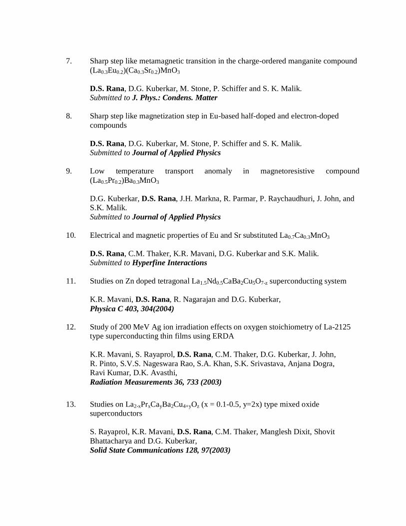
7. Sharp step like metamagnetic transition in the charge-ordered manganite compound (La0.3Eu0.2)(Ca0.3Sr0.2)MnO3
D.S. Rana, D.G. Kuberkar, M. Stone, P. Schiffer and S. K. Malik. Submitted to J. Phys.: Condens. Matter 8. Sharp step like magnetization step in Eu-based half-doped and electron-doped
compounds D.S. Rana, D.G. Kuberkar, M. Stone, P. Schiffer and S. K. Malik.
Submitted to Journal of Applied Physics 9. Low temperature transport anomaly in magnetoresistive compound
(La0.5Pr0.2)Ba0.3MnO3 D.G. Kuberkar, D.S. Rana, J.H. Markna, R. Parmar, P. Raychaudhuri, J. John, and
S.K. Malik. Submitted to Journal of Applied Physics
10. Electrical and magnetic properties of Eu and Sr substituted La0.7Ca0.3MnO3 D.S. Rana, C.M. Thaker, K.R. Mavani, D.G. Kuberkar and S.K. Malik. Submitted to Hyperfine Interactions 11. Studies on Zn doped tetragonal La1.5Nd0.5CaBa2Cu5O7-z superconducting system
K.R. Mavani, D.S. Rana, R. Nagarajan and D.G. Kuberkar, Physica C 403, 304(2004)
12. Study of 200 MeV Ag ion irradiation effects on oxygen stoichiometry of La-2125 type superconducting thin films using ERDA
K.R. Mavani, S. Rayaprol, D.S. Rana, C.M. Thaker, D.G. Kuberkar, J. John, R. Pinto, S.V.S. Nageswara Rao, S.A. Khan, S.K. Srivastava, Anjana Dogra, Ravi Kumar, D.K. Avasthi, Radiation Measurements 36, 733 (2003)
13. Studies on La2-xPrxCayBa2Cu4+yOz (x = 0.1-0.5, y=2x) type mixed oxide
superconductors S. Rayaprol, K.R. Mavani, D.S. Rana, C.M. Thaker, Manglesh Dixit, Shovit
Bhattacharya and D.G. Kuberkar, Solid State Communications 128, 97(2003)

14. Effect of Mo substitution on the superconductivity, flux pinning and critical currents of La1.5Nd0.5Ca1Ba2Cu5Oz
S. Rayaprol, Krushna Mavani, C.M. Thaker, D.S. Rana, R.G. Kulkarni, D.G. Kuberkar, Darshan C. Kundaliya and S.K. Mailk, Physica C, Vol. 391, 237 (2003)
15. Structural Investigations of La-2125 mixed oxide superconducting system
S. Rayaprol, Krushna Mavani, D.S. Rana, C.M. Thaker, R.S. Thampi, D.G. Kuberkar, R.G. Kulkarni, S.K. Malik, Journal of Superconductivity, Vol. 15, No.3, 211, June 2002
16. Effect of bandwidth and size disorder on the electronic and magnetic properties of LaMnO3 perovskite
C.M. Thaker, D.S. Rana, Krushna Mavani, S. Rayaprol, M. Shasrabudhe, S.I. Patil, N.A. Kulakarni and D.G. Kuberkar, Indian Journal of Engineering and Materials Sciences, Vol. 10, 324 (2003)
17. Effect of Pr-Ca substitution on the transport and magnetic behavior of LaMnO3
perovskite
C.M. Thaker, S. Rayaprol, Krushna Mavani, D.S. Rana, M. Sahasrabudhe, S.I. Patil, D.G. Kuberkar, Pramana - Journal of Physics, Vol. 58, Nos. 5&6, 1035, May & June 2002
18. Structural studies and Tc dependence in La2-xDyxBa2CayCu4+yOz type mixed oxide
8superconductors
S. Rayaprol, Krushna Mavani, C.M. Thaker, D.S. Rana, Nilesh A. Kulkarni, Keka Chakravorty, S.K. Paranjape, M. Ramanadham and D.G. Kuberkar, Pramana - Journal of Physics, Vol. 58, Nos. 5&6, 877, May & June 2002
19. Anomalous behavior in Y0.8Mo0.2MnO3 system
C.M. Thaker, D.S. Rana, Krushna Mavani, S. Rayaprol, M. Sahasrabudhe, S.I. Patil, Nilesh A. Kulkarni and D.G. Kuberkar, Solid State Physics (India), Vol. 44, 379 (2001)
20. Revival of Tc by Ca doping at Y site in YBa2(Cu1-xZnx)3O7-δ system
Krushna Mavani, S.Rayaprol, D.S. Rana, C.M. Thaker, S.K. Paghdar, R. Nagarajan, Nilesh A. Kulkarni, D.G.Kuberkar, Solid State Physics (India), Vol. 44, 341 (2001)
21. Cation Size Mismatch Dependent Structural and Transport Properties of Sr and Ba Doped La
0.5Pr
0.2Ca
0.3MnO
3
D.S. Rana, C.M.Thaker, Krushna Mavani, S.Rayaprol, D.G.Kuberkar, Solid State Physics (India), Vol. 45 (2002)
22. Variable Range Hopping in (LaEu)0.55(CaSr)0.45 MnO3 and
(LaTb)0.55(CaSr)0.45MnO3
D.S. Rana, C.M. Thaker, Krushna Mavani, S. Rayaprol, D.G. Kuberkar, Darshan C. Kundaliya, and S.K. Malik Proceedings of International conference on “Phonons in Condensed Materials, Bhopal (Phonons2K3), Feb 20-22, 2003”
23. Electrical and Magnetic Properties of (La0.25Nd0.25)(Ca0.25Sr0.25)MnO3 Manganite D. S. Rana, C. M. Thaker, K. R. Mavani, D. G. Kuberkar and S. K. Malik,
Solid State Physics, India, Vol. 46 (2003)
1. Visiting Students Research Programme (VSRP), during May 15 – July 7, 2000 at Tata Institute of Fundamental Research (TIFR), Mumbai.
2. International conference on “Advances in Superconductivity & Magnetism:
Materials, Mechanism & Devices” at Mangalore University, Mangalore, India (September 25-28, 2001)
3. DAE-BRNS Topical Meeting on PLD of thin films at Centre for Advance
Technology, India (November 26-28, 2001) 4. 44th DAE- Solid State Physics Symposium at Bhabha Atomic Research Centre,
Mumbai, India (December 26-30, 2001) 5. 13th Annual general meeting of Materials Research Society of India and theme
symposium on “Perspectives in Materials Characterization”, I ICT/ DMRL, Hyderabad, India (February 7-9, 2002)
6. One day seminar on Condensed Matter Physics at Sardar Patel University, Vallabh
Vidyanagar, India (March, 2002) 7. 45th DAE- Solid State Physics Symposium at Punjab University, Chandigarh, India
(December 26-30, 2002) 8. International conference on “Phonons in Condensed Matter Physics, Bhopal, Feb
20-22, 2003 (Phonons2K3)” held at Barkatullah University, Bhopal, India 9. 46th DAE- Solid State Physics Symposium at Jiwaji University, Gwalior, India
(December 26-30, 2003) 10. International workshop on Hyperfine Interaction, Feb 10-14, 2004”, M.S.
University, Baroda, India
*****
Scope for the future work
The problems investigated during the course of present thesis work are complete
and provide clear picture of the new contributions made. However, this thesis leaves
many open questions for the future investigations. A few of those are listed below.
1. Chapter 3 highlights an unusually large magnetoresistance ~99% at low
temperatures arising as results of extrinsic factors. Can such a large
magnetoresistance via extrinsic factor be tailored to occur at room temperature
over a wide temperature range? Chapter 3 also emphasizes the occurrence of
sharp step-like metamagnetic transitions in unconventional Eu-based compounds.
Earlier such step-like transitions were reported to occur mysteriously in Pr-based
compounds, thus, leaving an open question of contribution of any property
intrinsic to Pr-ion. The observation of step in Eu-based half-doped compounds
further leaves an open problem to be investigated that whether it occurs in other
rare-based compounds and is a property that manifests in phase-separated
manganites through interplay of tolerance factor and size-disorder.
2. Chapter 5 emphasizes the appearance of a low temperature resistivity minimum in
Ba-based compounds. Such kind of minimum is not very common in manganites.
We attribute its occurrence to the metallic disorder induced as a result of large
size variance via lattice distortion. In the present study, we have deduced this
possibility on the basis of results of one compound. However, it needs an
extensive study on the occurrence of this minimum in a series of compounds with
varying size-variance at A-site.

Index Contents Page
Chapter – 1 Introduction to CMR Materials
1.1 Introduction to manganite materials I-3
1.2 Various properties CMR manganites I-5
1.2.1 Electronic structure I-5
1.2.2 Zener-Double Exchange I-7
1.2.3 Electron-lattice coupling I-13
1.2.4 Complete spin polarization and half-metallic character I-15
1.2.5 Charge-ordering in manganites I-17
1.3 Applications of magnetoresistive materials I-18
1.4 Thin film technology I-20
1.5 Motivation of the present studies I-21
References I-24
Chapter – 2 Experimental techniques and characterization methods used
2.1 Synthesis methods II-1
2.1.2 Solid state method II-1
2.1.3 Pulsed Laser deposition of thin films II-2
2.2 Structural and morphological studies II-5
2.2.1 X-ray diffraction II-6
2.2.2 Atomic Forced Microscopy II-9
2.3 Electrical and magnetotransport properties studies II-11
2.2.3 D.c. four-probe method II-11
2.4 Magnetic susceptibility and magnetization measurements II-13
2.2.4 D.c. magnetization II-13
2.2.5 A.c susceptibility II-15
2.5 Specific heat measurements II-15
References II-19

Chapter – 3 Structure, electronic transport, magnetism, magnetoresistance
and specific heat of (La0.7-2xEux)(Ca0.3Srx)MnO3 (0.05 ≤ x ≤ 0.25)
and (La0.7-3xTbx)(Ca0.3Sr2x)MnO3 (0.025 ≤ x ≤ 0.125) compounds
3.1 (La0.7-2xEux)(Ca0.3Srx)MnO3; 0.05≤x≤0.25 series III-2
3.1.1 Structure III-2
3.1.2 Electronic transport III-4
3.1.3 Magnetic properties III-9
3.1.4 Specific measurements III-21
3.1.5 Magnetoresistance III-24
3.1.6 Summary and conclusions III-30
3.2 (La0.7-3xTbx)(Ca0.3Srx)MnO3; 0.025≤x≤0.125 series III-31
3.1.1 Structure III-31
3.1.2 Electronic transport III-33
3.1.3 Magnetic properties III-37
3.1.5 Magnetoresistance III-43
3.1.6 Conclusions III-44
References III-45
Chapter – 4 Effect of size-disorder on electronic transport and magnetism of
half-doped (LaTb)0.5(CaSr)0.5MnO3 and largely hole-doped
(LaR)0.55(CaSr)0.45MnO3 systems
4.1 Studies on (LaTb)0.5(CaSr)0.5MnO3 system IV-1
4.1.1 Structure IV-2
4.1.2 Magnetic properties IV-3
4.1.3 Electronic transport IV-5
4.1.4 Magnetoresistance IV-7
4.1.5 Conclusions IV-8
4.2 Studies on (LaR)0.55(CaSr)0.45MnO3 system IV-9
4.2.1 Structure IV-10

4.2.2 Electronic transport IV-11
4.2.3 Magnetic properties IV-14
4.2.4 Magnetoresistance IV-17
4.2.5 Conclusions IV-19
References IV-21
Chapter – 5
Investigations on low temperature resistivity minimum in
(La0.5Pr0.2)Ba0.3MnO3 polycrystalline bulk and epitaxial thin
films 5.1 Synthesis, structure and surface morphology V-1
5.1.1 Synthesis V-1
5.1.2 Structure V-2
5.1.3 Surface morphology V-3
5.2 Resistivity and magnetization V-5
5.2.1 Resistivity V-5
5.2.2 Magnetization V-8
5.3 Low temperature resistivity minimum V-8
5.4 Magnetoresistance V-15
5.5 Conclusions V-19
References V-21

Chapter – 1
Introduction to CMR Materials
1.1 Introduction to manganite materials I-3
1.2 Various properties CMR manganites I-5
1.2.1 Electronic structure I-5
1.2.2 Zener-Double Exchange I-7
1.2.3 Electron-lattice coupling I-13
1.2.4 Complete spin polarization and half-metallic character I-15
1.2.5 Charge-ordering in manganites I-17
1.3 Applications of magnetoresistive materials I-18
1.4 Thin film technology I-20
1.5 Motivation of the present studies I-21
References I-24

1
Introduction to CMR materials
The materials play a great role in improving the living standards of human life and,
therefore, search for new materials have been a constant attractions for human beings. As
the time passes, the need based priority of new materials prompts the human beings for
research in materials which results in discovery of new materials in different eras. A
glimpse at the history of materials research in twentieth century reveals that the magnetic
materials are probably second mostly investigated materials after semiconductors. Many
classes of magnetic materials have tremendously contributed in the various aspects of
human life. In same direction, the oxide materials have many fascinating magnetic and
electrical properties which make them investigated by researchers in great interest. In late
twentieth century, the discovery of high temperature superconductivity in cuprates oxides
attracted a sizeable fraction of materials scientists to put their efforts in tailoring these
materials for applications. Contemporarily, the magnetic materials have tremendously
contributed in the various aspects of human life. Primarily, the magnetic memory devices
have taken the major research endeavors due to their potential in conquering the time and
space. Amongst all, magnetoresistive materials are a kind of magnetic materials, which
have found large application as magnetic memory read heads.
Magnetoresistance (MR) is the fall or resistivity on the application of magnetic field.
It is defined quantitatively as
100%0
0 ×−
=ρ
ρρ HMR
where ρ0 and ρH are the resistivities in absence and presence of magnetic field
respectively. MR may be negative and positive depending upon the fall or rise in the
resistivity respectively on the application of magnetic field.
Magnetic multilayer devices such as alternate layers of Fe/Cr and Cu/Co coupled
antiferromagnetically to each other exhibit a negative magnetoresistance (MR). The
negative MR in this kind of materials is as large as 20%-50% and hence termed as “Giant
magnetoresistance (GMR)” [1-3]. Owing to such a large negative magnetoresistance, these
materials have been in application for a quite some time. However, the search for better
magnetoresistive materials never ended and in 1993, the ABO3 perovskite structured oxide
materials of type (R1-xAx)MnO3 (R= trivalent rare-earth cation, A=divalent cation) came
into research focus, when Von Helmolt et al. [4] and Charara et al. [5] almost
2
Introduction to CMR materials
simultaneously reported a huge magnetoresistance in these compounds. Simultaneously, in
similar materials, Jin et al. [6] reported magnetoresistance ~ 99% and owing to the
strength of magnetoresistance, coined a new term as “Colossal Magnetoresistance
(CMR)”. Following this report, the manganite oxide materials exhibiting huge
magnetoresistance are also known as CMR materials. These materials showed their
strength in applications such as magnetic read heads, bolometry, electric field effect
devices, hybrid heterostructure devices, etc. [7] which will be discussed later. During last
half century, the different forms of magnetoresistance have evolved having origin in
different physical aspects. These are as follows.
A. Anisotropic magnetoresistance (AMR)
Anisotropic magnetoresistance arises due difference in resistivity when magnetic
field is applied to parallel and perpendicular direction of current [8,9]. In certain
ferromagnetic metallic systems, the resistivity increases when applied magnetic field is
perpendicular to the current whereas the resistivity decreases when magnetic field is
perpendicular to the direction of current. Hence, the magnetic field induced anisotropy in
resistivity of different current vectors (parallel and perpendicular) gives rise to anisotropic
magnetoresistance.
B. Granular and tunneling magnetoresistance
It arises in the granular systems in which the grain boundaries act as insulator barrier
or junction to the conduction of carriers and results in the spin dependent scattering of
carriers [10,11]. The granular magnetoresistance has its origin in spin polarized
conduction of carriers. The application of magnetic field diminishes this spin dependent
insulating barrier. This reduces the scattering of carriers resulting in magnetoresistance
called granular magnetoresistance. The tunneling magnetoresistance [12] arises when
artificial junctions are developed as insulating barrier for conduction of current and same
physical origin as that of granular magnetoresistance.
C. Giant magnetoresistance (GMR)
This is form of magnetoresistance observed in metallic multilayers such as Fe/Cr,
Co/Cu, in which trilayer junctions of two ferromagnetic layers separated by a non
magnetic space layer are formed [1-3]. The non-magnetic layer is coupled
3
Introduction to CMR materials
antiferromagnetically with the adjacent ferromagnetic layer via RKKY interactions and
also the exchange biasing of one magnetic layer to antiferromagnetic layer [13]. The
conduction of current between two ferromagnetic layers through space layer depends upon
the relative orientation of the spin direction of the conduction electron with respect to
magnetic moment of the space layer. The magnetic field enhances the conduction of
electrons resulting in magnetoresistance of the order of 50%. Owing to large amount of
MR, name Giant magnetoresistance was given to emphasize the strength of MR in these
materials.
D. Colossal magnetoresistance (CMR)
Recently, the magnetoresistance as large as ~100% was observed in manganites.
This was an extraordinarily large magnetoresistance as compared to previously observed
GMR. Therefore, to emphasize the strength of MR in these compounds, a new term called
“colossal magnetoresistance (CMR)” was coined [6]. The origin of MR in manganites is
quite different than the origin of other forms of MR discussed above. The CMR is an
intrinsic property of crystal structure and has its origin in the spin disorder of conduction
electron, which can be suppressed by the application of the magnetic field resulting in
large magnetoresistance [4-6]. The discovery of CMR in manganites and its relation to
various electronic and magnetic properties rejuvenated the research interest in similar
compounds. Since manganites appear promising candidates both from basic research and
applications point of view, a major fraction of materials scientist has contributed to the
better understanding of these materials. This thesis is devoted to the understanding of
various physical properties of complex manganites system and some efforts to evaluate the
application potentiality of few compounds.
1.1 Introduction to manganite materials exhibiting colossal
magnetoresistance (CMR)
The CMR materials are in focus of research not only because of the exotic property
of magnetoresistance but also due to many other properties involving a rich variety of
physics. These materials have been investigated since long for their electronic transport,
which includes interest in insulator-metal (I-M) transition, the nature of electronic
transport, charge-ordering, etc.; magnetism comprising various magnetic phase transitions
correlated with electronic transition temperatures; temperature and carrier density
4
Introduction to CMR materials
dependent structural and orbital correlation; and various other charge, spin and orbital
correlation and dynamics, etc [see for a review refs 14-18]. The various physical
properties of manganites were though studied in long back in 1950s and 1960s [19-24] but
the observation of negative colossal magnetoresistance in 1993 [4-6] redirected the
research interests in these materials. The CMR property made these compounds to be most
widely studied oxide materials after the cuprate oxide high temperature superconductors
(HTSC).
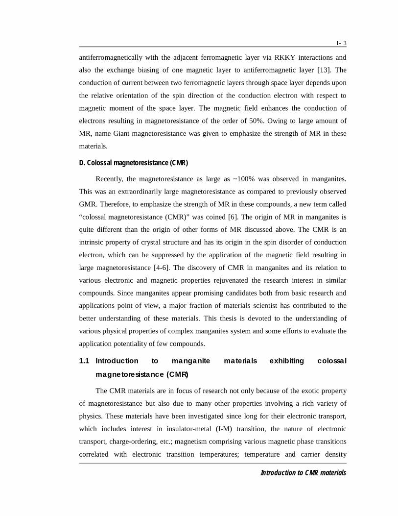
Figure 1: An ABO3 type of perovskite structure. LaMnO3 crystallizes in this type of
structure in which La occupies A-site and Mn occupies B-site. MnO6
octahedron is shown at the corner of unit cell.
The LaMnO3 is a basic compound having ABO3 type perovskite structure. A is body
centred cation and Mn ion occupies the octahedral position surrounded by six oxygen ions,
thus, forming a MnO6 octahedron [23]. It is a paramagnetic insulator but shows a
paramagnetic to antiferromagnetic transition at a temperature of around 150K. Here, the
cations La and Mn exist in +3 oxidation state. Partial substitution of trivalent cation at A-
site by a divalent cation results into a composition with a general formula (R1-xAx)MnO3
(R = La, Pr, Nd, etc.; A = Ca2+, Sr2+, Ba2+, etc.). This causes an amount (equal to x) of
Mn3+ to convert in Mn4+ state. Since Mn exists in mixed valence state, these compounds
are also known as “mixed-valent manganites”. In mixed-valence manganites of this type,
when 0 < x < 0.5, Mn4+ content is less than 50% and holes are the charge carriers and
hence in such a condition the manganites are called hole-doped compounds. The hole-
doped compounds exhibit ferromagnetic metallic (FMM) behavior below a certain critical
A
B
O
5
Introduction to CMR materials
temperature and after a certain minimum amount of Mn4+ is generated. The largest
transition appears for x = 1/3. At higher hole-doping, the columbic interactions overcome
the mobility of carriers, which further results in fall in transition temperature. At
0.5 < x < 1, Mn3+ is less than 50% and electrons are the charge carriers and manganites
obeying this condition are known as electron-doped systems. In such a condition, the
number of conduction links decrease than that of Mn4+ coupled antiferromangetic (AF)
content, hence, an insulating AF behavior manifests. The compounds with x = 0.5 are the
half-doped systems [15-18].
1.2 Various properties of CMR manganites
1.2.1 Electronic structure
The LaMnO3 is one of the basic parent compounds, which has been most widely
studied for substitutional studies. This compound has been identified to possess
characteristics of both the Mott insulators and charge transfer insulators. The
Mott-Hubbard interaction energy, Udd, required for creating a dn+1dn-1 excitation in an
array of dn ions, lies in range of 4-5 eV. Similarly, the charge-transfer energy, Upd, (energy
for creating p5dn+1 charge excitation from p6dn) has been estimated around 5eV. Many
groups have estimated the Udd and Upd between 4-6 eV [25-27]. Since both these energies
are of comparable magnitude, LaMnO3 is believed to posses both Mott-Hubbard type and
charge transfer type insulator character. In 3d transiton metal group, the early oxides are
Mott-Hubburd insulators whereas the last members are charge-transfer insulators. A
detailed review of transition metal oxides has been given by A.K. Raychaudhuri [28]. This
supports that, for the oxide in the middle of series such as LaMnO3, both Udd and Upd
become comparable. In undoped LaMnO3, Mn exists in 3+ oxidation state wherein due to
doping of divalent cation, a fraction of Mn3+ state is converted to Mn4+ state. Mn3+ is a 3d
ion with four electrons in spin-up orbitals whereas all the spin-down orbitals are vacant.
The five d-orbitals are split by crystal field of oxygen in 3 t2g and 2 eg orbitals. These
levels are separated by an energy ~1.5 eV for Mn3+ and 2.4 eV for Mn4+ [29]. The strong
Hund’s rule coupling ensures the parallel alignment of electron spin in 3 t2g and 2 eg
energy levels. In principle the pure compound is supposed to be cubic in structure but the
cation mismatch at A-site cause the structural distortion. When the symmetry is lower than
cubic, the degeneracy of the eg and t2g levels is lifted by Jahn-Teller (J-T) distortion and J-
6
Introduction to CMR materials
T separation lies in the range ~ 0.5-1 eV [30]. This distortion compresses of the MnO6
octahedra along ab-plane and elongates along c-plane, thus, resulting in reduced overlap of
Mn 3d-orbitals and oxygen p-orbitals. Therefore, due to the structural distortion of MnO6
octahedra, the conduction in the compounds having all Mn3+ ions is not possible. The
structural distortion caused by Jahn-Teller effect is long-range order effect and is more
effective when Mn3+ content is very large. In the absence of eg electron Mn4+ remains
unaffected by such a distortion. Here, it should be mentioned that the Jahn-Teller
distortion is volume preserving whereas the other kind of distortion called breathing mode
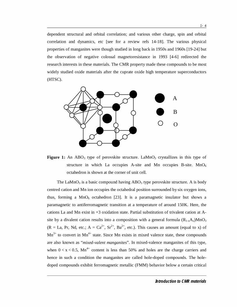
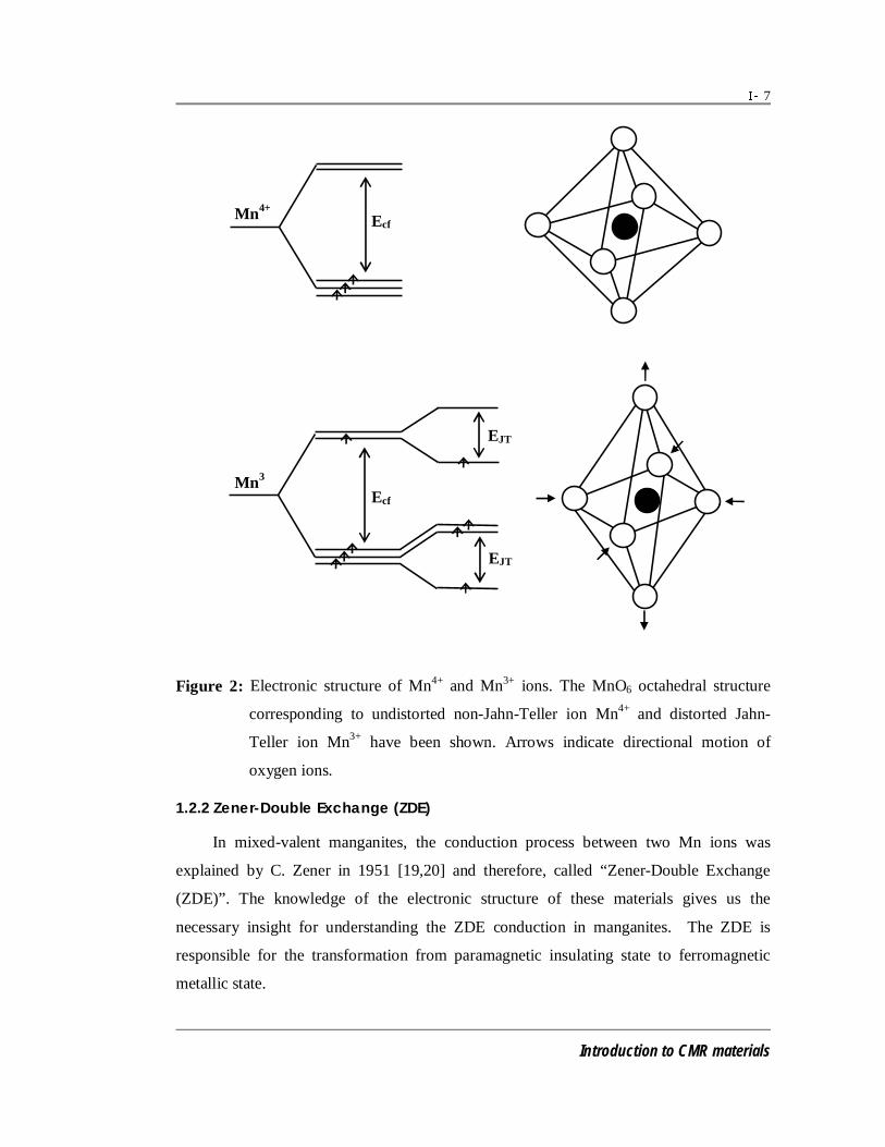
distortion is uniaxial and not volume preserving. Figure 2 displays the electronic energy
levels of Mn3+ and Mn4+ ions with corresponding MnO6 octahedron.
7
Introduction to CMR materials
Figure 2: Electronic structure of Mn4+ and Mn3+ ions. The MnO6 octahedral structure
corresponding to undistorted non-Jahn-Teller ion Mn4+ and distorted Jahn-
Teller ion Mn3+ have been shown. Arrows indicate directional motion of
oxygen ions.
1.2.2 Zener-Double Exchange (ZDE)
In mixed-valent manganites, the conduction process between two Mn ions was
explained by C. Zener in 1951 [19,20] and therefore, called “Zener-Double Exchange
(ZDE)”. The knowledge of the electronic structure of these materials gives us the
necessary insight for understanding the ZDE conduction in manganites. The ZDE is
responsible for the transformation from paramagnetic insulating state to ferromagnetic
metallic state.
Mn3
+
EJT
EJT
Ecf
Mn4+
Ecf
8
Introduction to CMR materials
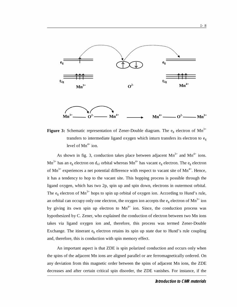
Figure 3: Schematic representation of Zener-Double diagram. The eg electron of Mn3+
transfers to intermediate ligand oxygen which inturn transfers its electron to eg
level of Mn4+ ion.
As shown in fig. 3, conduction takes place between adjacent Mn3+ and Mn4+ ions.
Mn3+ has an eg electron on dz2 orbital whereas Mn4+ has vacant eg electron. The eg electron
of Mn3+ experiences a net potential difference with respect to vacant site of Mn4+. Hence,
it has a tendency to hop to the vacant site. This hopping process is possible through the
ligand oxygen, which has two 2p, spin up and spin down, electrons in outermost orbital.
The eg electron of Mn3+ hops to spin up orbital of oxygen ion. According to Hund’s rule,
an orbital can occupy only one electron, the oxygen ion accepts the eg electron of Mn3+ ion
by giving its own spin up electron to Mn4+ ion. Since, the conduction process was
hypothesized by C. Zener, who explained the conduction of electron between two Mn ions
takes via ligand oxygen ion and, therefore, this process was termed Zener-Double
Exchange. The itinerant eg electron retains its spin up state due to Hund’s rule coupling
and, therefore, this is conduction with spin memory effect.
An important aspect is that ZDE is spin polarized conduction and occurs only when
the spins of the adjacent Mn ions are aligned parallel or are ferromagnetically ordered. On
any deviation from this magnetic order between the spins of adjacent Mn ions, the ZDE
decreases and after certain critical spin disorder, the ZDE vanishes. For instance, if the
eg eg
t2g t2g
Mn4+ O2-
Mn3+ O2- Mn4+
Mn3+ Mn4+ O2- Mn3+
9
Introduction to CMR materials
spins of adjacent Mn ions are in antiferromagnetic order, there will be no ZDE. In such a
case the superexchange (SE) will be favored. However, the detailed discussion of SE is
beyond the scope of this thesis. The relation of the ZDE with the spin magnetic order of
the Mn ions was given by Anderson and Hasegawa [31] in 1961, who have defined the
transfer integral depending on the angle between the spin moments of adjacent Mn ions.
They described the ZDE process using a Hamiltonian
∑∑ −−=i
iiHij
ii SJcctH .† σσσ
where t is the nearest neighbor hopping integral, σic† and σic are creation and annihilation
operators. The transfer integral is created when spins are parallel and annihilated for anti
parallel spins. Si is the eg i is the t2g core spin (3/2). The second
term in the above equation gives the onsite Hund’s rule coupling. This terms ensures that
lowest energy is obtained when the spins of eg and t2g electrons are aligned parallel to each
other. In case of strong Hund’s rule coupling, coupling constant JH tends to ∞ and the
hopping amplitude of electrons is defined by transfer integral, tij, given by
=
2
cos0
ijij tt
θ
where, ij is the angle between the neighboring spins. The transfer integral and
Hamiltonian given above explains the concomitant occurrence of Tp and TC. Also, the
resistivity may be related to the Curie temperature (TC) by a relation given by
=
CTT
xe
ah2
ρ
where, x is the fraction of Mn4+ and a is lattice parameter. This relation indicates
concomitant occurrence of TC and I-M transition.
However, there are some other factors which are responsible for these electronic and
magnetic transition temperatures. These are: 1) hole-density, 2) The Goldschmidt
tolerance factor and 3) the size-variance at A-site.
10
Introduction to CMR materials
1. Hole-density
For a particular hole doped (R1-xAx)MnO3 system, the ZDE induced ferromagnetic
metallic (FMM) behavior appears at certain minimum threshold amount (x) of
hole-density. For instance, this minimum hole-density x is 0.18 for A = Ca and x is 0.11
for A = Sr. However, the largest transition appears for x = 1/3 and this amount is called as
optimal doping content. At higher hole-doping, the increasing columbic interactions start
dominating the kinetic energy of the carriers and the I-M transition disappears at higher
divalent doping contents and electron-doped compositions are AFM insulators [15-18].
2. The Goldschmidt tolerance factor
Goldschimdt tolerance factor (t) [32] is a characteristic of cationic and anionic radii,
given by the relation
)(2 OB
OA
rr
rrt
+><+><
=
where, <rA> and <rB> are the average A-site and B-site cation radii respectively. rO is
the radius of oxygen. Tolerance factor is ideally 1 with a cubic structure with an angle of
180o between Mn-O-Mn bonds. These compounds possesses a stable perovskite structure
when 0.75 < t < 1. As the tolerance factor decreases, the bandwidth of the itinerant eg
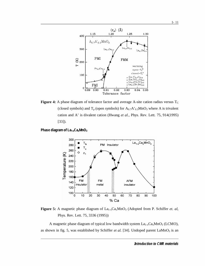
electron decreases and hence result in the TC and Tp. Depending on the bandwidth of the eg
electron, the manganites can be broadly classified into three major systems: 1) low
bandwidth system, 2) intermediate bandwidth system and 3) large bandwidth. The
manganite system such as Pr1-xCaxMnO3 in which the bandwidth of eg is not sufficient for
conduction of carriers is called low bandwidth systems. However, the low bandwidth
systems can exhibit the I-M transition on the application of magnetic field. A manganite
system, La1-xCaxMnO3 which exhibits transition below room temperature is an
intermediate bandwidth system, whereas a system, La1-xSrxMnO3 is large bandwidth
system because it becomes ferromagnetic-metallic well above room temperature. As
shown in fig. 4, a phase diagram giving relationship of electrical and magnetic properties
with the tolerance factor was given by Hwang et al.
11
Introduction to CMR materials
Figure 4: A phase diagram of tolerance factor and average A-site cation radius versus TC
(closed symbols) and Tp (open symbols) for A0.7A’0.3MnO3 where A is trivalent
cation and A’ is divalent cation (Hwang et al., Phys. Rev. Lett. 75, 914(1995)
[33]).
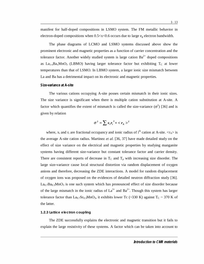
Phase diagram of La1-xCaxMnO3
Figure 5: A magnetic phase diagram of La1-xCaxMnO3 (Adopted from P. Schiffer et. al,
Phys. Rev. Lett. 75, 3336 (1995))
A magnetic phase diagram of typical low bandwidth system La1-xCaxMnO3 (LCMO),
as shown in fig. 5, was established by Schiffer et al. [34]. Undoped parent LaMnO3 is an

12
Introduction to CMR materials
A-type antiferromagnetic (AFM) insulator. The system is AFM and FM insulator
for 0 < x < 0.18 and possesses a concomitant FM metallic character for 0.18 < x < 0.5. All
the compositions in this doping range exhibit large CMR effect. In 0.48 < x < 0.52
compositions, the FM metallic state transforms to charge-ordered antiferromagnetic
ground state at a certain critical temperature. The AFM state in this range is of CE-type.
When x>0.52, a long-range C-type AFM order sets in. The end member CaMnO3 with all
Mn4+ content is G-type AFM insulator.
Phase diagram of La1-xSrxMnO3
Figure 6: A magnetic phase diagram of La1-xSrxMnO3 (adopted from Urushibara et al.,
Phys. Rev. B 51, 14103).
After the rejuvenation of research in manganites, Urushibara et al. [35] established
the electronic phase diagram of large bandwidth systems, La1-xSrxMnO3 (LSMO), shown
in figure 6. This systems displays Curie temperature at above room temperature at around
~ 380 K for x = 0.33. The compounds are spin canted insulators for 0<x<0.09 and is FM
insulator in the range 0.09<x<0.16. The LSMO systems is FM metallic coupled to CMR
effect when the compositions span a range 0.16<x<0.6. The solid solutions above x>0.6
are not possible due to chemical phase segregation of SrMnO3. Here, it may also be noted
that exotic properties like coexistence charge and orbital ordering and AFM order do not
13
Introduction to CMR materials
manifest for half-doped compositions in LSMO system. The FM metallic behavior in
electron-doped compositions when 0.5<x<0.6 occurs due to large eg electron bandwidth.
The phase diagrams of LCMO and LSMO systems discussed above show the
prominent electronic and magnetic properties as a function of carrier concentration and the
tolerance factor. Another widely studied system is large cation Ba2+ doped compositions
as La1-xBaxMnO3 (LBMO) having larger tolerance factor but exhibiting TC at lower
temperatures than that of LSMO. In LBMO system, a larger ionic size mismatch between
La and Ba has a detrimental impact on its electronic and magnetic properties.
Size-variance at A-site
The various cations occupying A-site posses certain mismatch in their ionic sizes.
The size variance is significant when there is multiple cation substitution at A-site. A
factor which quantifies the extent of mismatch is called the size-variance (σ2) [36] and is
given by relation
∑ ><+= 222Aii rrxσ
where, xi and ri are fractional occupancy and ionic radius of ith cation at A-site. <rA> is
the average A-site cation radius. Martinez et al. [36, 37] have made detailed study on the
effect of size variance on the electrical and magnetic properties by studying manganite
systems having different size-variance but constant tolerance factor and carrier density.
There are consistent reports of decrease in TC and Tp with increasing size disorder. The
large size-variance cause local structural distortion via random displacement of oxygen
anions and therefore, decreasing the ZDE interactions. A model for random displacement
of oxygen ions was proposed on the evidences of detailed neutron diffraction study [36].
La0.7Ba0.3MnO3 is one such system which has pronounced effect of size disorder because
of the large mismatch in the ionic radius of La3+ and Ba2+. Though this system has larger
tolerance factor than La0.7Sr0.3MnO3, it exhibits lower Tc (~330 K) against TC ~ 370 K of
the latter.
1.2.3 Lattice electron coupling
The ZDE successfully explains the electronic and magnetic transition but it fails to
explain the large resistivity of these systems. A factor which can be taken into account to
14
Introduction to CMR materials
explain the large resistivity in manganites near and above TC is the electron lattice
coupling [38]. Millis et al. have emphasized the role of static and dynamic Jahn-Teller
effect on the structural and transport aspects of manganites [39]. This can be explained as
follows. The eg and t2g energy levels of Mn3+ ion are Jahn-Teller (J-T) split with a large
local lattice distortion which result in J-T type distortion of the MnO6 octahedron. This
produces a potential minimum which tends to trap the eg electron in its orbital. This
coupling is strong enough to localize the eg electron. The formation of such a self trapped
electronic state is called a polaron. The polaron formation is generally associated with the
deformable medium and the eg electron trapped in J-T distorted medium presents a similar
scenario. The conduction of polaron is thermally activated with a poor probability of
hopping and, hence, the manganites have large resistivity above TC. The question is why
resistivity is large near and above TC and how ZDE is not above TC. There are two energy
levels competing, one tends to localize the eg electron and the other tends to delocalize it.
This is given by a constant λ = Elatt/teff, where Elatt is the energy of the electron-phonon
coupling in the absence of hybridization which tends to localize the electron and teff is the
kinetic energy of the electron. At higher temperatures, teff is sufficiently small and,
therefore, large value of λ localizes the electron. However, as the temperature is decreased
through TC the lattice electron coupling gets weak and the growing ferromagnetic fraction
increases teff. This decreases λ, thus, resulting in ZDE induced metallic behavior in
manganites.
There have been few theoretical studies [39,41] depicting a strong dependence of λ
on the resistive behavior of manganites. Here, it may be mentioned that λ can also be
tuned by various other factors such as chemical substitution (by changing R and A), carrier
density, magnetic field, temperature, etc. There are some strong evidences of Jahn-Teller
coupling as evident from changes in Mn-O bond lengths over a some given temperature
range. In theoretical calculations, a strong local structural distortion has been anticipated
in the high temperature insulating regime. However, these local distortions almost
disappear below TC. Booth et al. [42] carried out extended X-ray absorption fine structure
(EXAFS) measurements on various compositions of La1-xCaxMnO3 and found clear
evidence of such local distortions. They observed that LaMnO3 has long range distortion,
whereas the other end member has no distortion due to absence of eg electron. The

15
Introduction to CMR materials
intermediate members have large distortions at higher temperature above TC. Hence, all
the theoretical predictions and experimental evidences indicate the importance of electron-
phonon coupling in controlling various electronic, magnetic and structural properties.
Also, it has been established that the conduction in the paramagnetic region occurs
through thermally activated polaron hopping. In literature, many experimental evidences
supported by theoretical interpretations exist. Jaime et al. [43,44] have studied the polaron
transport by resistivity and thermopower measurements. It has been further emphasized
that there is a crossover from small polaron conduction to large polaron behavior at TC.
There are also evidences of variable range hopping (VRH) both of Mott’s [45] and
Schovsky-Effros (SE) type [46]. As evident from a largely published data, VRH type
conduction is dominant in compounds exhibiting lower Curie temperatures. As the
temperature decreases, the thermal excitations are not sufficient for nearest neighbour
hopping. However, carriers find a potential difference to hop to farther distances through
grain boundaries called VRH type of conduction.
1.2.4 Complete spin polarization and half-metallic character
In mixed-valent manganites, there is a net difference between the spin up and spin
down electronic states. This is characteristic of half-metallic property where conduction
occurs by majority of conduction carriers. The conduction band is fully spin-polarized
(complete saturation magnetization) due to the half metallic character. Hence, in
manganites, below TC, the conduction occurs through the spin polarized carriers. Ideally,
the complete spin-polarization is possible at 0K [47]. However, at sufficiently low
temperatures well below TC such as at 5K, the spin polarization is assumed to be almost
complete. There are many experimental evidences in support of spin polarization below TC
and the spin polarized state increases as the temperature decreases. A major experimental
evidence of the existence of spin polarized conduction is the inter-grain spin polarized
tunneling (SPT) magnetoresistance at low temperature. The SPT magnetoresistance
increases with decreasing temperature below TC which is consistent with the spin
polarized character.
16
Introduction to CMR materials
Causes of CMR effect
The study of CMR property comprises a crucial part of experimental, theoretical and
application aspects of mixed-valence manganites. This is one of most widely explored
property because it evaluates these materials for their application potentiality. The CMR
property is dominant in the vicinity of Tp, in all the different structural forms such as
granular polycrystalline, single crystals and epitaxial single crystalline thin films.
Interestingly, at low temperatures (well below Tp), both the granular and the single
crystalline forms exhibit drastically different CMR properties. This reflects the grain
boundary contributions to CMR property. Mainly, we can attribute the CMR to the
following two reasons.
1. The magnetic field induced reduction in magnetic spin disorder at Mn-O-Mn bonds.
The application of magnetic field forces the parallel alignment of spins. This increases the
ZDE and, hence, a large MR in the vicinity of Tp [4-6]. This is an intrinsic property of
crystal structure and common in both polycrystalline and single crystal forms of material.
2. The magnetic field induced reduction in spin dependent scattering at grain
boundaries. The contribution of grain boundaries to MR increases as the temperature
decreases from Tp. As the temperature decreases, the spin polarization of d-band of Mn
ions increases and at very low temperature, the d-band is almost fully spin-polarized. The
fully spin-polarized carriers can tunnel easily through the misaligned grain boundaries on
the application of magnetic fields. The resulting MR is called the inter-grain spin-
polarized tunneling (SPT) [48-50]. Within a grain, a carrier can easily travel owing to the
parallel alignment of spins. When it approaches the grain boundary, the misaligned
magnetic moment of the next grain scatters it, thus increasing the resistivity. The applied
magnetic field aligns the magnetic moments of all the grains in its own direction. This
enhances the tunneling of carriers at the grain boundaries and, therefore, the resulting
magnetoresistance is a grain boundary contribution.
In past, there have been many efforts through chemical substitution to synthesize
manganite materials which can exhibit large room temperature MR in low fields of few
hundreds Oe but resulted into a limited success. A fundamental limitation is that the MR
decreases with increasing TC. Nowadays, the focus has changed to tailor these materials
for low field large MR through artificial grain boundary and multilayer devices.
17
Introduction to CMR materials
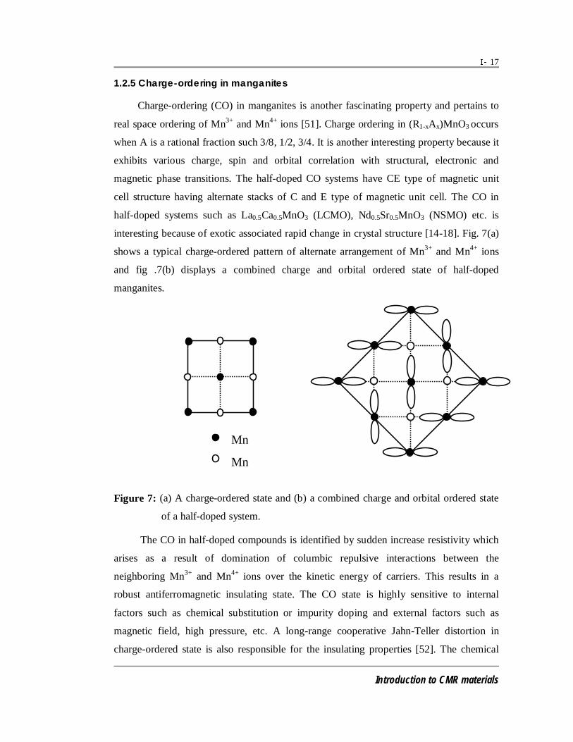
1.2.5 Charge-ordering in manganites
Charge-ordering (CO) in manganites is another fascinating property and pertains to
real space ordering of Mn3+ and Mn4+ ions [51]. Charge ordering in (R1-xAx)MnO3 occurs
when A is a rational fraction such 3/8, 1/2, 3/4. It is another interesting property because it
exhibits various charge, spin and orbital correlation with structural, electronic and
magnetic phase transitions. The half-doped CO systems have CE type of magnetic unit
cell structure having alternate stacks of C and E type of magnetic unit cell. The CO in
half-doped systems such as La0.5Ca0.5MnO3 (LCMO), Nd0.5Sr0.5MnO3 (NSMO) etc. is
interesting because of exotic associated rapid change in crystal structure [14-18]. Fig. 7(a)
shows a typical charge-ordered pattern of alternate arrangement of Mn3+ and Mn4+ ions
and fig .7(b) displays a combined charge and orbital ordered state of half-doped
manganites.
Figure 7: (a) A charge-ordered state and (b) a combined charge and orbital ordered state
of a half-doped system.
The CO in half-doped compounds is identified by sudden increase resistivity which
arises as a result of domination of columbic repulsive interactions between the
neighboring Mn3+ and Mn4+ ions over the kinetic energy of carriers. This results in a
robust antiferromagnetic insulating state. The CO state is highly sensitive to internal
factors such as chemical substitution or impurity doping and external factors such as
magnetic field, high pressure, etc. A long-range cooperative Jahn-Teller distortion in
charge-ordered state is also responsible for the insulating properties [52]. The chemical
Mn3+
Mn4+

18
Introduction to CMR materials
substitution on the CO half-doped systems such as LCMO and NSMO melts the CO
through a I-M transition [53,54]. In low bandwidth half-doped systems such as
Pr0.5Ca0.5MnO3, the CO state does not melt through I-M transition but results in the
magnetic field sensitive electronic phase separation. Though considerable research has
been carried out on CO systems, there is a large scope to investigate the effect size
variance and average A-site cation radius on other rare-earth based half-doped systems.
1.3 Applications of magnetoresistive materials
The manganites have potential for applications in various fields exploiting the
property of CMR, spin polarized conduction of carriers and I-M transition. A few
applications are listed below.
1. Magnetic memory read heads and spin valves
The CMR effect in manganites has shown a great application potential in magnetic
memory devices. Using this property, these materials can be utilized as magnetoresistive
read heads. In magnetic recording thin film devices, the data is acquired and hence a
magnetic flux is stored and generated. A magnetic memory read head uses the property of
magnetoresistance to retrieve data, which is stored as magnetic bits. The stored data
(which has magnetic flux) is sufficient to change direction of magnetization, which results
in change in the resistivity by a few percent. The CMR property in manganites has its
origin in field induced increase in ferromagnetic spin ordering and fall of resistivity;
therefore, these materials can be tailored to design need based magnetic memory read
heads. The manganites can be made as good memory read heads if the MR% near the
room temperature (300K ± 50K) remains almost constant and can be as high as 20% in a
field of few hundred Oe. However, due to some limitations, the present scenario does not
allow these materials to be used as magnetoresistive read heads. The efforts are still going
on to achieve desired room temperature MR through multilayer, spin valves and spin
tunneling devices. These devices show an enhanced MR in the temperature where the spin
polarized tunneling magnetoresistance dominates. A spin valve consists of two CMR
ferromagnetic electrodes separated by space layer of metallic and insulating compounds
[55]. Initially, epitaxial metallic layers such as LaNiO3, LaSrCoO3, SrRuO3, etc. were
grown between two CMR electrodes [56] but resulted in a negative impact on
magnetoresistance. However, introduction of an epitaxial insulating layer of compounds

19
Introduction to CMR materials
such as SrTiO3, LaAlO3, MgO, etc. between the CMR electrodes resulted in large
enhancement of CMR effect [57]. In all these trilayer junction devices, it is evident that as
the spin-polarization increases, the CMR effect increases. Therefore, a large low field
CMR effect occurs only at low temperatures.
2. Bolometer IR sensors
The manganites exhibit large non-linear variation of resistivity with the temperature
near I-M transition and, hence, are potential candidates for being used as bolometer
sensors [58-60]. The temperature coefficient of resistance (TCR) defined as
1/R(dR/dT)×100 evaluates the potentiality of any materials for bolometer sensors. A good
commercial bolometer possesses a TCR of ~ 4%. In certain manganite compounds, for
example La0.7Ca0.3MnO3, can exhibit TCR as high as 10-18% over the same temperature
range. The TCR in most of the manganites increases manifolds on substitution of smaller
size cation at A-site, but it occurs quite below room temperature which restrict them from
applications.
3. Hybrid HTSC-CMR devices
In manganites, the spin polarized conduction of carriers at low temperatures has
been a boon to devise new hybrid structures. One such device that can be thought is the
CMR-HTSC spin injection device. In this direction, FET structures can be fabricated using
CMR materials as ferromagnetic layers epitaxially grown with YBCO layers. In this
device, the spin polarized electrons from the manganite layers are injected into the HTSC
channel layers and the I-V characteristics as a function of gate current is studied [61,62].
Here, the properties largely differ when CMR layer with spin polarization character is
replaced with the one having unpolarized electrons as carriers. Spin polarized carrier
increases the pair breaking efficiency by many fold.
Manganites can also be thought of being used as flux to voltage convertors. CMR
based sensors having large magnetoresistance in a field of few thousand Oe can be useful
as voltage to flux convertor in a certain temperature range (over which it exhibits
spectacularly large MR) [63]. Also, the Meissner effect of HTSC oxides can be used as
magnetic lens to enhace the flux coupling to a CMR detector thereby enhancing its
sensitivity [64].
20
Introduction to CMR materials
4. Electric field effect devices
Manganites have also been tested in FET devices. CMR channels based FETs with
either para-electric dielectric layer such as SrTiO3 (STO) or a ferroelectric layer such as
PZT have shown remarkable properties depending upon the nature of layer introduced. For
STO the polarity has no effect on the response of the device and peak resistivity shifts to
lower temperatures [65]. The lack of polarity in STO based device may be an indication of
effects induced by the spin polarized character rather than charge injection. This device
can help in understanding the fall of polarization with increasing Curie temperature. The
ferroelectric gate based devices show large changes in resistance (as large as ~ 100%),
which make them attractive for potential non-volatile applications [66].
Apart from applications based on physical properties, mixed-valent manganites also
have potential for applications owing to their chemical properties of catalytic activity of
Mn3+ and Mn4+ valence. The chemical properties include the catalysis of automobile
exhausts, oxygen sensors and solid electrolytes in fuel cells. The alkali ion substituted
manganites are useful in such kind of applications. The monovalent cation (such as Na+,
K+, etc.) substituted LaMnO3 can be used for reduction and decomposition of NO and
divalent cation (such as Ca2+, Sr2+, Ba2+, etc.) have been used for NO reduction, CO
oxidation and NH3 oxidation [16].
1.4 Thin film technology
The applications of most of the technological relevant compounds are possible in
thin films form of the material [18, 56]. The thin films are structurally more homogenous,
with acceptable noise signal and can be tailored according to the need. In the
semiconductor industry, many technologically important devices used are in thin film
form. In the magnetic industry too, the thin films are thought to be really the structural
form of the material, which can be used when application of the pertinent materials
becomes feasible. This has prompted many scientists all over the world to study these
materials, both in polycrystalline and thin film forms. The idea of study in thin film form
has seen development of many tools for the best possible synthesis based on chemical and
physical principles such as; ion beam sputtering, MOCVD (Molecular chemical vapor
deposition), molecular beam epitaxy (MBE), chemical solution deposition (CSD), pulsed
laser deposition (PLD), etc. Among all these techniques, PLD has emerged as most
21
Introduction to CMR materials
efficient and convenient technique for deposition of thin films of mixed oxide compounds.
This technique is most widely used for preparing the manganite thin films.
Pulsed Laser Deposition (PLD) of manganite thin films
Pulsed laser deposition (PLD) of manganite epitaxial single crystalline thin films is
interesting because it helps in understanding the clean physics in the absence of various
defects and polycrystalline grain boundaries. It is evident from various studies in
manganites that a clear contribution of crystal structure to physical properties doesn’t
manifest clearly in polycrystalline compounds. Zin et al. [6] were the first to report the
MR studies on manganite thin films. Later, A. Gupta et al. [49] have emphasized the role
of grain boundaries by comparing the MR behavior of polycrystalline and single
crystalline epitaxial thin films. Subsequently, many studies were based on the thickness
dependent and substrate-film lattice mismatch and strain induced modifications in
transport and MR properties [67-72]. Importance of the effect of surface morphology on
the electronic transport and magnetic properties has also been emphasized [73-74]. Thin
films are a form of the material which can find real applications from technological point
of view. Therefore, a clear understanding of physical properties of thin film forms of a
material becomes utmost important. In manganites, the thin film synthesis becomes even
more important because this may enhance the efforts for device fabrication such as
multilayer devices having a low field large MR at nearly room temperature with
application suitability.
1.5 Motivation for the present work
The motivation for the present work has been manifolds. The present work is a blend
of investigations of various physical properties aimed both at the understanding of the
physics involved and evaluating a few compounds from applications point of view. During
the present work, a contribution is made in increasing the understanding pertinent to
simultaneous size disorder and carrier density effects in modifying the structural,
electronic and magnetic properties. It has been demonstrated that, at very low
temperatures, disorder induces anomalously large MR~99%. A separate attempt has been
made to understand the effect of size-disorder in the half-doped and heavily holed-doped
systems, having a critical constant <rA>. A fascinating part of this thesis comprises the
investigations on the metamagnetic behavior of Eu-based half-doped and electron-doped
22
Introduction to CMR materials
compounds. The evolution of sharp step-like metamagnetic transitions in Eu-doped
compounds reveals that the rich class of metamagnetism is not mysteriously limited
Pr-based manganites and, hence, any property intrinsic to rare-earth ions have no impact
on this fascinating property.
Another aspect of effect of increasing size-disorder is the anomalous low
temperature resistivity minimum which manifest after the onset of the metallic region.
Such a behavior could arise from various reasons such as grain boundary effect, weak
localization and anomalous Kondo effect. To understand the origin of this behavior, we
have synthesized the epitaxial single crystalline thin films using PLD technique. An
attempt has been made to resolve whether the low temperature resistivity minimum is due
grain boundary effect and/or electron-electron scattering.
Details of the all the subsequent chapters comprising thesis are given below
Chapter 2 of the thesis deals with the various experimental tools and methods such as
x-ray diffraction (XRD), d.c. four-probe method for resistivity measurements, d.c. and a.c.
magnetization measurements, magnetoresistance measurements, specific heat using
relaxation calorimetry; their need and importance as a characterization tool has been
discussed. The working and operation of the various instruments such as Pulsed Laser
Deposition system, Atomic Forced Microscopy, SQUID magnetometer, Physical Property
Measurement System employed to characterize of the materials has also been given.
Chapter 3 deals with the real research problem and efforts to resolve some issues in
the related field. The synthesis of (La0.7-2xEux)(Ca0.3Srx)MnO3 (0.05 ≤ x ≤ 0.25) system
has been made to keep <rA> constant at 1.205Å but results in an increase in size-disorder
and carrier density simultaneously. A rich class of Eu-based sharp step like
metamagnetism in charge ordered composition has been major outcome of this work. In
the same spirit, various physical properties of the system (La0.7-3xTbx)(Ca0.3Sr2x)MnO3
(0.025 ≤ x ≤ 0.125) in which <rA> ~ 1.207Å have been studied.
Chapter 4 deals with the effect of size-disorder on the electronic and magnetic
properties of a half-doped system (LaTb)0.5(CaSr)0.5MnO3 and largely hole-doped
(LaR)0.55(CaSr)0.45MnO3 systems. In half doped system, it has been shown that, initially,
the increasing size-disorder drives the compounds to exhibit I-M transition but when size-
23
Introduction to CMR materials
disorder increases largely, the increasing lattice strain decreases the ferromagnetic
interactions. In more than optimally doped system, the electronic and magnetic behavior in
this system is highly dependent on small changes in size disorder.
Chapter 5 is dedicated to the thin film deposition and study various structural,
electronic transport, magnetic and the low temperature electron localization effects. In our
group, we have studied La0.5Pr0.2Ba0.3MnO3 in bulk polycrystalline form for its structural,
electrical and magnetic properties. This sample exhibits a low temperature resistivity
minimum around a temperature of 40 K. To elucidate whether this is a grain boundary
effect and / or electron-electron scattering at low temperatures, we have synthesized this
sample both in polycrystalline and thin film forms. A comparative study of polycrystalline
bulk and single crystal epitaxial thin films has been carried out.

24
Introduction to CMR materials
References
1. M.N. Baibich, J.M. Baroto, A. Fert, F.N. Vandau, F. Petroff, P. Etienne, G.
Creuget, A. Freiderich, J. Chagelas, Phys. Rev. Lett. 61, 2472 (1988).
2. A. Fert, A. Barthelemy, P. Etienne, S. Lequiou, R. Loloee, D.K. Lottis, D.H.
Mosca, W.P. Pratt, P.A. Schroeder, J. Magn. Magn. Mater. 104, 1712 (1992).
3. G. Binash, P. Grunberg, F. Saurenbath, W. Zinn, Phys. Rev. B 39, 4828 (1989).
4. R. Von Helmolt, J. Wecker, B. Holzapfel, L. Schultz, K. Samwer, Phys. Rev.
Lett. 71, 2331 (1993).
5. K. Chahara, T. Ohno, M. Kasai, Y. Kosono, Appl. Phys. Lett. 63, 1990 (1993).
6. S. Zin, T.H. Tiefel, M. McCormack, R.A. Fastnacht, R. Ramesh, L.H. Chen,
Science 264, 413 (1994).
7. T. Venktesan, M. Rajeswari, Z.W. Dong, S.B. Ogale, R. Ramesh, Phil. Trans.
Roy. Soc. A 356, 1661 (1998).
8. A.B. Pippard, Magnetoresistance in Metals, Cambridge University Press,
Cambridge, 1998.
9. Thin Film Resistive Sensors, Ed. By P. Ciureanu, S. Middelhoek, Institute of
Physics Publishing, Bristol, 1992.
10. H.Y. Hwang, S.-W. Cheong, N.P. Ong, B. Batlogg, Phys. Rev. Lett. 77, 2041
(1996).
11. J.S. Hellman, B. Abeles, Phys. Rev. Lett. 37, 1429 (1976).
12. J.S. Moodera, L.S. Kinder, T.M. Wong, R. Meservey, Phys. Rev. Lett. 74, 3273
(1995).
13. V.S. Speriosu, B. Dieny, P. Humbert, B.A. Gurney, H. Lefakis, Phys. Rev. B 44,
5358 (1991).
14. “Colossal Magnetoresistance, charge ordering and other related properties of rare
earth manganates”, ed. by C. N. R. Rao and B. Raveau, World Scientifics
Publishing Company (1998).
25
Introduction to CMR materials
15. “Magnetoresistive oxides” Y. Tokura, Gordon and Breach publishes, London
(2000).
16. “Mixed valent manganites” J.M.D. Coey, M. Viret, S. Von Molnar, Advances in
Physics 48, 167-293 (1999).
17. A.P. Ramirez, J. Phys: Condens. Matter 9, 8171 (1999).
18. CMR manganites: Physics, thin films and devices, J. Phys. D: Appl. Phys. 36,
R127-R150 (2003).
19. C. Zener, Phys. Rev. 81, 440 (1951).
20. C. Zener, Phys. Rev. 82, 403 (1951).
21. P.G. de Gennes, Phys. Rev 118, 141 (1960).
22. E.O. Wollen, W.C. Koehler, Phys. Rev. 100, 545 (1955).
23. G.H. Jonker, J.H. Van Santen, Physica (Utrecht) 16, 337 (1950).
24. G.H. Jonker, Physica 22, 707 (1956).
25. J. Zaanen, G.A. Sawatzky, J.W. Allen, Phys. Rev. Lett. 55, 418 (1985).
26. J. Zaanen, G.A. Sawatzky, J. Solid-st. Chem. 88, 8 (1990).
27. J.-H. Park, C.T. Chen, S.-W. Cheong, W. Bao, G. Meigs, V. Chakarian, Y.U.
Idzerda, Phys. Rev. Lett. 76, 4215 (1996).
28. A.K. Raychaudhuri, Advances in Physics 44, 21-46 (1995).
29. M. Abbate, F.M.F. De Groot, J.C. Fuggle, A. Fujimori, O. Strebel, F. Lopez, M.
Domke, G. Kaindl, G.A. Sawatzky, M. Takano, Y. Takeda, H. Eisaki, S. Uchida,
Phys. Rev. B 46, 4511 (1992).
30. J.B. Goodenough, Annu. Rev. Mater. Sci. 28, 1 (1998).
31. P.W. Anderson, H. Hasegawa, Phys. Rev. 100, 675 (1955).
32. Geochemistry, by V. Goldschmidt, Oxygen University Press (1958).
33. Hwang, S.-W. Cheong, P.G. Radaelli, M. Marezio, B. Batlogg., Phys. Rev. Lett.
75, 914(1995).
26
Introduction to CMR materials
34. P. Schiffer, A.P. Remirez, W. Bao, S.-W. Cheong, Phys. Rev. Lett. 75, 3336
(1995).
35. Urushibara, Y. Moritomo, T. Amira, A. Asamitsu, G. Kido and Y. Tokura, Phys.
Rev. B 51, 14103 (1995).
36. L.M. Rodríguez-Martinez, J.P. Attfied, Phys. Rev. B 54, 15622 (1996).
L.M. Rodríguez-Martinez, J.P. Attfied, Phys Rev. B 58, 2426 (1998).
37. L.M. Rodríguez-Martinez, J.P. Attfied, Phys Rev. B 63, 24424 (2000).
38. A.J. Millis et al, Phys. Rev. Lett. 74, 5144 (1995); A.J. Millis, Nature 392, 147
(1998).
39. A.J. Millis, B.I. Shriaman, R. Mueller, Phys. Rev. Lett. 77, 175 (1996); A.J.
Millis, Phys. Rev. B 53, 8434 (1996); M. Quitjada, J. Carne, J.R. Simpson, H.D.
Drew, K.H. Ahn, A.J. Millis, R. Shreekala, R. Ramesh, M. Rajeshwari, T.
Venktesan, Phys. Rev. B 58, 16093 (1998).
40. H. Roder, J. Zang, A.R. Bishop, Phys. Rev. Lett. 76, 1356 (1996).
41. J. Zang, A.R. Bishop, H. Roder, Phys. Rev. B 53, 8840 (1996).
42. C.H. Booth, F. Bridges, G.H. Kwei, J.M. Lawrence, A.L. Cornelius, J.J.
Neumeier, Phys. Rev. Lett. 80, 853 (1998).
43. M. Jaime, M.B. Salamon, M. Rubinstein, R.E. Treece, J.S. Horwitz, D.B.
Chrisey, Phys. Rev. B 54, 11914 (1996).
44. M. Jaime, H.T. Hardner, M.B. Salamon, M. Rubinstein, P. Dorsey, D. Emin,
Phys. Rev. B 56, 951 (1997).
45. D. Emin and T Holstein, Phys. Rev. B 13, 647 (1976).
46. A. L. Efros and B.L. Shklovskii, J. Phys. C 8, L49 (1975).
47. J.-H Park, E. Vesokovo, H.-J. Kin, C. Kwon, R. Ramesh, T. Venktesan, Nature
392, 794 (1998).
48. H. Y. Hwang, S.-W Cheog, N. P. Ong, and B. Batlogg, Phys. Rev. Lett. 77, 2041
(1996).

27
Introduction to CMR materials
49. A. Gupta, G. Q. Gong, G. Xiao, P. R. Duncombe, P. Lecoeur, P. Trouilloud, Y.
Y. Wang, V. P. Dravid and J. Z. Sun, Phys. Rev. B 54, 15629 (1996).
50. P. Raychaudhuri, K. Sheshadri, P. Taneja, S. Bandyopadhyay, P. Ayuub, A.K.
Nigam, R. Pinto, Sujeet Chaudhuri, S.B. Roy, Phys. Rev. B 59, 13919 (1999).
51. C.N.R. Rao, A.K. Cheetam, Chem. Mater 10, 2714 (1998).
52. S. K. Mishra, S. Rahul Pandit and S. Satpathy, J. of Phys.: Condens. Matter 11,
8561 (1999).
53. P.V. Vanitha, P.N. Santhosh, R.S. Singh and C.N.R. Rao, J.P. Attfield, Phys.
Rev. B 59, 13539 (1999).
54. Y.Q. Gong, Ian Maclaren, X.F. Duan, Z.H. Wang and B.G. Shen, J. Appl. Phys.
90, 488 (2001); Y.Q. Gong, Ian Maclaren, X.F. Duan, Z.H. Wang and B.G. Shen,
Appl. Phys. Lett. 78, 2157 (2001).
55. B. Dieny, V.S. Speriosu, S. Metin, S.S. Perkin, B.A. Gurney, P. Baumgart, D.R.
Wilhoit, J. Appl. Phys. 69, 4774 (1991).
56. T. Venktesan, M. Rajeshwari, Zi-Wen Dong, S.B. Ogale, R. Ramesh, Phil.
Trans. R. Soc. Lond. A 356, 1661 (1998).
57. J.Z. Sun, W.J. Gallagher, G. Xiao, Appl. Phys. Lett. 69, 3266 (1996).
58. M. Rajeshwari, C.H. Chen, A. Goyal, C. Kwon, M.C. Robson, R. Ramesh, T.
Venktesan, S. Lakeou, Appl. Phys. Lett. 68, 3555 (1996).
59. M. Rajeshwari, A. Goyal, R. Shreekala, S.E. Lofland, S.M. Bhagat, R. Ramesh,
T. Venktesan, Appl. Phys. Lett. (1998).
60. A. Goyal, M. Rajeshwari, R. Shreekala, S.E. Lofland, S.M. Bhagat, T. Boettcher,
C. Kwon, R. Ramesh, T. Venktesan, Appl. Phys. Lett. 71, 1718 (1998).
61. V.A. Vas’ko, A.V. Larkin, P.A. Kraus, K.R. Nikolaev, D.E. Grupp, C.A.
Nordman, A.M. Goldman, Phys. Rev. Lett. 78, 1134 (1997).
62. Z.W. Dong, R. Ramesh, T. Venktesan, M. Johnson, Z.Y. Chen, S.P. Pai, R.
Shreekala, R.P. Sharma, C.J. Lobb, R.L. Greene, Appl. Phys. Lett. 71, 1718
(1997).
63. T. Kimura, Y. Yomoika, H. Kuwahara, A. Asamitsu, M. Tamura, T. Tokura,
Sience 274, 1698 (1996).
64. Z.W. Dong, T. Boettcher, C.H. Chen, I. Takeuchi, M. Rajeshwari, T. Venktesan,
Appl. Phys. Lett. 69, 3432 (1996).
28
Introduction to CMR materials
65. S.B. Ogale, V. Talyansky, C.H. Chen, R. Ramesh, R.L. Greene, T. Venktesan,
Phys. Rev. Lett. 77, 1159 (1996).
66. S. Mathew, R. Ramesh, T. Venktesan, J. Benedetto, Science 276, 238 (1997).
67. A.J. Millis, T. Darling, A. Migliori, J. Appl. Phys. 83, 1588 (1998).
68. G.M. Gross, F.S. Razavi, R.B. Praus, H.-U Hebermeier, J. Magn. Magn. Mater
211, 22 (2000).
69. Y. Suzuki, H.Y. Hwang, S.-W. Cheong, R.B. Van Dover, Appl. Phys. Lett. 71,
140 (1997).
70. Y. Suzuki, H.Y. Hwang, S.-W. Cheong, T. Siegrist, R.B. Van Dover, A.
Asamitsu, Y. Tokura, J. Appl. Phys. 88, 7064 (1998).
71. F. Tsui, M.C. Smoak, T.K. Nath, C.B. Eom, Appl. Phys. Lett. 76, 2421 (2000).
72. K. Steenback, T. Hebisreuther, C. Dubourdieu, J.-P. Senatuer, Appl. Phys. Lett
80, 3361 (2002).
73. O.J. Gonzales, G. Bistue, E. Catano, F.J. Gracia, J. Magn. Magn. Mater. 222, 199
(2000)
74. G. Van Tendeloo, O.I. Lebedev, A. Amelinckx, J. Magn. Magn. Mater. 211, 73
(2000).
Chapter – 2
Experimental techniques and characterization
methods used
2.1 Synthesis methods II-1
2.1.2 Solid state method II-1
2.1.3 Pulsed Laser deposition of thin films II-2
2.2 Structural and morphological studies II-5
2.2.1 X-ray diffraction II-6
2.2.2 Atomic Forced Microscopy II-9
2.3 Electrical and magnetotransport properties studies II-11
2.2.3 D.c. four-probe method II-11
2.4 Magnetic susceptibility and magnetization measurements II-13
2.2.4 D.c. magnetization II-13
2.2.5 A.c susceptibility II-15
2.5 Specific heat measurements II-15
References II-19
1
Experimental techniques and characterization methods used
2.1 Synthesis methods
The synthesis of good quality material is a key to obtain the desired physical
properties. Therefore, the selection of sample preparation method is a crucial factor. The
synthesis of polycrystalline bulk samples is broadly divided into two categories namely;
1) solid state reaction method and 2) chemical route comprising sol-gel technique, nitrate
route, co-precipitation technique, etc. [1-3]. Owing to its simplicity, all the bulk
polycrystalline samples studied during the course of present work have been synthesized
using the solid state reaction method. In order to prepare a single-phase sample, the
conditions during any reaction are very important. During synthesis, the parameters such
as temperature, pressure, gas flow and time for the reaction are needed to be varied
according to the phase requirements in the sample. Mapping of all variables has to be
made to find the conditions, which are best for each material and phase.
2.1.1 Solid state reaction method
During the course of present study, all the bulk polycrystalline samples have been
synthesized with solid-state reaction method [1]. As the name suggests, the solid form of
the constituents are reacted at high temperatures for a certain minimum period of time.
The general procedure involved in solid-state reaction method for producing mixed
valent manganite oxides is described below.
All starting materials are high purity powders of carbonates, oxides, nitrides, etc.
They are preheated for appropriate time and temperature to remove the low temperature
volatile impurities. Powders are then weighed in proportionate quantity according to the
desired composition. In the solid state reaction, for the reaction to take place
homogeneously, it is very important to mix and grind the powders thoroughly for long
duration to obtain homogeneous distribution in required proportions of the desired
stoichiometric compound. The proper grinding of mixed powders using pestle-mortar
decreases the particle size which is necessary for obtaining close contact among the
atoms so the right material is formed. This powdered mixture is then heated in air at
about 950oC. During the first calcination, CO2 is liberated from the mixture. After the
calcinations, the compounds are reground, palletized and sintered for a long time (~100
hours) in the temperature range of 1100oC - 1250oC. Before every sintering of samples,
the obtained fine black powders are pressed into cylindrical pellets. Many intermediate
2
Experimental techniques and characterization methods used
grindings are required to get appropriate phase formation and phase purity. These
heatings in atmospheric conditions are required to obtain phase formation and to release
the remaining CO2, if any. The final sintering is carried out a sufficient high temperature
(in the range 1300-1400oC) to get the better crystallization. The furnace is turned off and
the samples are left inside to cool down to at least 300oC.
The solid-state reaction method is proved to be the most suitable for synthesizing
reproducible samples of CMR manganite oxides. The similar Oxygen annealing is not
important for manganites as these materials posses good stability of oxygen
stoichiometry.
2.1.2 PLD method for thin films
The Pulsed Laser Deposition (PLD) method for deposition of thin films of mixed
oxides uses the knowledge principles of optical science and materials science [4]. Laser
has proved to be a powerful tool in many such applications. It is very useful in material
processing due to its narrow frequency bandwidth, coherence and high power density.
The light beam of laser can be intense enough with high energy per unit area to vaporize
the hardest and most heat resistant materials [5,6]. Due to its high precision, reliability
and spatial resolution, it is widely used for deposition of the thin film, modification of
materials, heat treatment, welding and micro-patterning. Apart from these, multi-
component materials can be ablated and deposited onto substrate to form stoichiometric
thin films. This Procedure is called Pulsed Laser Deposition. This is an efficient method
to synthesize thin films by utilizing the technique of laser ablation. This method for thin
film synthesis is applicable to many materials; in particular it is versatile method to
ceramic materials [2]. Today, PLD is one of the fastest growing thin-film processes for
synthesizing multi-components films. This process transports elements from one location
(target material) to another (substrate) by supplying energy to elements from a laser
source. Ideally, such a process coats the surface with a pure film of the correct
composition. Fig. 1 shows the schematic diagram of PLD apparatus along with target
holder, substrate holder, focusing lens, etc. The PLD method involves evaporation of a
solid target material in an Ultra High Vacuum (UHV) chamber by means of short and
high energy laser pulses.

3
Experimental techniques and characterization methods used
Figure 1: A schematic representation of PLD apparatus.
Conventional arrangement for PLD for the synthesis of thin solid films is
characterized by the following features:
1. A focused laser beam is directed to the target to ablate the material.
2. The target holder is rotated along an axis or (x, y) - scanned in the focal plane of
the laser beam to achieve a constant ablation rate. The vacuum chamber is made
of stainless steel and is evacuated down to 10-6 bar by using a turbo pump.
3. Well polished substrate located at a typical separation from the target is
stationary or rotated for homogenization of the deposited material. To form a film
with required stoichiometry and the temperature of the substrate may be kept
between room temperature and 850oC. This temperature depends upon the nature
of material used for ablation.
4. A gas supply is often provided to produce desired chemical reactions during film
growth. Mixed oxide materials are prone to loose oxygen during the deposition.
Therefore, during deposition of such oxide materials, certain optimum partial
pressure of oxygen is maintained during the deposition. The O2 partial pressure
was maintained at 400mTorr during the manganite thin film deposition presented
in this thesis.
4
Experimental techniques and characterization methods used
The manganite thin films synthesized in the present course of work are synthesized
by PLD method using KrF excimer gas laser. The details of deposition condition and
parameters used for PLD method used are discussed in chapters 5.
Principle of PLD
The principle of pulsed laser deposition is a very complex physical phenomenon. It
comprises many processes in a chain namely, 1) the physical process of the laser-
material interaction on solid target followed by, 2) the formation of plasma plume with
high energetic species and 3) the transfer of the ablated material through the plasma
plume onto the heated substrate surface. Firstly, the pulsed laser beam is focused onto
the surface of the target. This laser beam strikes the surface of the target material with
sufficiently high energy and short pulse duration, which results into the rapid heating up
of the target elements up to their evaporation temperatures. Because of such a high
energy, the elements are dissociated from the target surface and ablated out with
stoichiometry as in the target. In most materials, the ultraviolet radiation is absorbed by
only the outermost layers of the target up to a depth of ~ 1000 Å. The extremely short
laser pulses (<50 ns) rapidly increase temperature of the surface to thousands of degrees
Celsius, but the bottom of the target remains virtually unheated. Such un-equilibrium
heating produces a flash of evaporated elements that deposit on the substrate, producing
a film with composition identical to that of the target surface. Rapid deposition of the
energetic ablation species helps to raise the substrate surface temperature. In this respect
PLD tends to demand a lower substrate temperature for crystalline film growth.
Advantages of PLD
Several aspects of PLD are beneficial over other methods for deposition of thin
films. It produces a highly forward-directed and confined plume of materials, which can
be deposited with less contamination than the unconfined plasma in a sputtering process.
In addition, PLD is incredibly precise. In complex multi target system deposition with
conventional deposition methods, the various elements come from different sources. To
produce the right mixture in the deposited film, the rate of arrival of each species must be
monitored and controlled. This becomes especially difficult when large background gas
pressures are used during the deposition. PLD does not require such monitoring, because
the composition of the film replicates the composition of the target. Due to the short laser
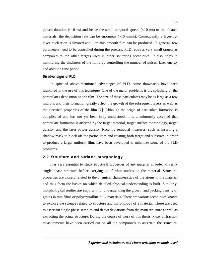
5
Experimental techniques and characterization methods used
pulsed duration (~10 ns) and hence the small temporal spread (≤10 ms) of the ablated
materials, the deposition rate can be enormous (~10 mm/s). Consequently a layer-by-
layer nucleation is favored and ultra-thin smooth film can be produced. In general, few
parameters need to be controlled during the process. PLD requires very small targets as
compared to the other targets used in other sputtering techniques. It also helps in
monitoring the thickness of the films by controlling the number of pulses, laser energy
and ablation time period.
Disadvantages of PLD
In spite of above-mentioned advantages of PLD, some drawbacks have been
identified in the use of this technique. One of the major problems is the splashing or the
particulates deposition on the film. The size of these particulates may be as large as a few
microns and their formation greatly affect the growth of the subsequent layers as well as
the electrical properties of the film [7]. Although the origin of particulate formation is
complicated and has not yet been fully understood, it is unanimously accepted that
particulate formation is affected by the target material, target surface morphology, target
density, and the laser power density. Recently remedial measures, such as inserting a
shadow mask to block off the particulates and rotating both target and substrate in order
to produce a larger uniform film, have been developed to minimize some of the PLD
problems.
2.2 Structure and surface morphology
It is very essential to study structural properties of any material in order to verify
single phase structure before carrying out further studies on the material. Structural
properties are closely related to the chemical characteristics of the atoms in the material
and thus form the basics on which detailed physical understanding is built. Similarly,
morphological studies are important for understanding the growth and packing density of
grains in thin films or polycrystalline bulk materials. There are various techniques known
to explore the science related to structure and morphology of a material. These are used
to ascertain single phase samples and detect deviations from the main structure as well as
extracting the actual structure. During the course of work of this thesis, x-ray diffraction
measurements have been carried out on all the compounds to ascertain the structural
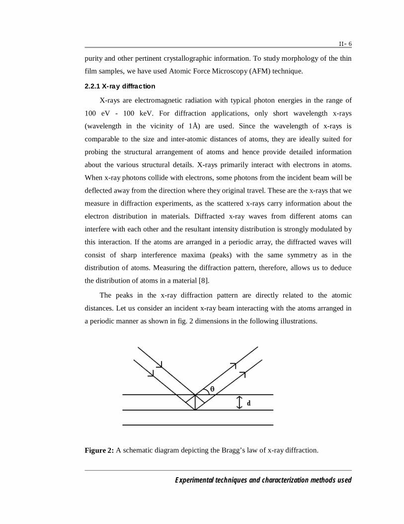
6
Experimental techniques and characterization methods used
purity and other pertinent crystallographic information. To study morphology of the thin
film samples, we have used Atomic Force Microscopy (AFM) technique.
2.2.1 X-ray diffraction
X-rays are electromagnetic radiation with typical photon energies in the range of
100 eV - 100 keV. For diffraction applications, only short wavelength x-rays
(wavelength in the vicinity of 1Å) are used. Since the wavelength of x-rays is
comparable to the size and inter-atomic distances of atoms, they are ideally suited for
probing the structural arrangement of atoms and hence provide detailed information
about the various structural details. X-rays primarily interact with electrons in atoms.
When x-ray photons collide with electrons, some photons from the incident beam will be
deflected away from the direction where they original travel. These are the x-rays that we
measure in diffraction experiments, as the scattered x-rays carry information about the
electron distribution in materials. Diffracted x-ray waves from different atoms can
interfere with each other and the resultant intensity distribution is strongly modulated by
this interaction. If the atoms are arranged in a periodic array, the diffracted waves will
consist of sharp interference maxima (peaks) with the same symmetry as in the
distribution of atoms. Measuring the diffraction pattern, therefore, allows us to deduce
the distribution of atoms in a material [8].
The peaks in the x-ray diffraction pattern are directly related to the atomic
distances. Let us consider an incident x-ray beam interacting with the atoms arranged in
a periodic manner as shown in fig. 2 dimensions in the following illustrations.
Figure 2: A schematic diagram depicting the Bragg’s law of x-ray diffraction.

7
Experimental techniques and characterization methods used
The horizontal line forms a set of planes in the crystal resulting from the periodic
arrangement of atoms. For a given set of lattice plane with an inter-plane distance of d,
the condition for a diffraction (peak) to occur can be simply written as
2d sinθ = nλ
which is known as the Bragg's law, named after W.L. Bragg, who first proposed it. In the
equation, λ is the wavelength of the x-ray, θ is the scattering angle, and n an integer
representing the order of the diffraction peak. The Bragg's Law is one of most important
laws used for interpreting x-ray diffraction data. It is important to note that although we
have used atoms as scattering points in this example, Bragg's Law applies to scattering
centers consisting of any periodic distribution of electron density. In other words, the law
holds true if the atoms are replaced by molecules or collections of molecules, such as
colloids, polymers, proteins and virus particles.
Powder XRD (X-ray Diffraction) is perhaps the most widely used x-ray diffraction
technique for characterizing polycrystalline materials [9,10]. The term 'powder' really
means that the crystalline domains are randomly oriented in the sample and the sample is
usually in a powdery form, consisting of fine grains of single crystalline material to be
studied. When the 2-D diffraction pattern is recorded, it shows concentric rings of
scattering peaks corresponding to the various d spacings in the crystal lattice. The
positions and the intensities of the peaks are used for identifying the underlying structure
of the material. The powder method is used to determine the value of the lattice
parameters accurately. Lattice parameters are the magnitudes of the unit vectors a, b and
c which define the unit cell for the crystal. The structural studies for the samples under
present studies are performed by XRD and Rietveld refinement of XRD data. The
Rietveld analysis is described below.
Rietveld Analysis
The Rietveld analysis [11,12] is a refinement method for powder diffraction
patterns to study the crystallographic and nuclear and magnetic structures. To find the
magnetic structure, polarized neutrons are needed whereas x-ray diffraction provides the
information about the crystallographic structure. Once the structure is known, the
analysis starts with an approximation of the lattice parameters and calculates the
diffraction pattern for the structure. The structure is described with a large number of

8
Experimental techniques and characterization methods used
parameters as is the experimental set-up. There are nine parameters for the experimental
equipment: the wavelength, the scale factor, the zero point for 2θ and six parameters for
a polynomial background. Most of the parameters have to be refined. The gradient for
the weighted sum of squared difference between the calculated intensities and the
measured intensities, Mp, can be determined relative to these parameters. The gradient is
then used to change the parameters and this is repeated until a minimum in the Mp
function is reached. The definition of Mp and the profile factors were taken from the
FULLPROF manual.
Mp is defined as
∑ −=i
icioiP YYWM 2 [2.2]
where wi is a weight function, yio is the observed intensity at angular step i, yic is the
corresponding calculated intensity. To control the quality of the refinement, several
agreement factors were calculated. The profile factor,
∑∑ −
=
iio
iicio
wp Y
YY
R
|| [2.3]
the weighted profile factor,
2/1
2
2
exp
−=
∑∑
iioi
iicioi
YW
YYW
R [2.4]
the expectation factor,
2/1
2exp
+−=
∑i
ioiYW
CPNR [2.5]
the Bragg factor,
R
I I
IBragg
jo jcj
joj
=−∑
∑
| |
[2.6]
and the goodness of fit,
9
Experimental techniques and characterization methods used
2
exp
2
=
R
Rwpχ [2.7]
Here, Ijo and Ijc are the observed and calculated integrated intensities for the different
Bragg peaks j, and (N-P+C) is the number of degrees of freedom. N is the number of
points in the pattern, P the number of refined parameters and C the number of strict
constraint functions.
The refinements of the XRD of the samples were made using FULLPROF program.
The order of refining the parameters was: the scale factor, the zero point for 2θ, five of
the background parameters, the cell parameters, three of the peak shape parameters, the z
co-ordinates, the isotropic displacement parameters, the occupation numbers, the fourth
peak shape parameter, the anisotropic displacement parameters and the last background
parameter. A few different routes to convergence were tried to confirm an optimal result.
The R factors are good indicators if a route is not converging to a reliable result.
2.2.2 Atomic Force Microscopy (AFM)
Atomic Force Microscopy (AFM) is a probe to study the surface morphology of
conducting or non-conducting materials. The basic objective of the operation of the AFM
is to measure the atomic level forces between a sharp probing tip attached to a cantilever
spring and a sample surface [13]. A sharp probe on a flexible lever (cantilever) scans the
material. While scanning, the cantilever responds to encountered features on the material
surface and measured attractive or repulsive forces between a tip and the sample are
recorded. These reactions produce an image of the material surface showing the presence
of humps and valleys on the surface, resembling a surface topographic map. Images are
produced by scanning the sample relative to the probing tip and measuring the deflection
of the cantilever as a function of lateral position. Now most AFM employ an optical
lever technique. The diagram illustrates how this works; as the cantilever flexes, the light
from the laser is reflected onto the split photo-diode or position sensitive detector. By
measuring the difference signal (A-B) or position respectively, changes in the bending of
the cantilever can be measured (fig. 3). Basically, there are two methods used for AFM:
(a) Contact mode and (b) Non-contact mode.

10
Experimental techniques and characterization methods used
Figure 3: (Top panel) Working of optical cantilever in AFM & (bottom panel) an
experimental set up of AFM. [14].
Contact mode AFM
In this method, the cantilever remains in contact with the surface during scanning
and hence it is called contact mode AFM [13]. The cantilever deflects to follow the
contours and by this, it encounters variations on the surface. The accurate topographical
maps of the surface for different type of samples can be produced by this method. There
are some drawbacks of using this method. Due to continuous contact of the cantilever on
the surface of the sample, the surface may get damage that can change both the resulting
image and properties of the material. Hence, this method is suitable only for certain type
of materials. To counter such problems in contact mode method, it was modified and a
new method called ‘tapping mode’ was developed. In this mode, the tip intermittently
touches the surface, instead of being dragged and introducing damage as in contact
mode. The cantilever oscillates at a frequency, as it scans the surface. When the tip

11
Experimental techniques and characterization methods used
begins to slightly touch the surface, a sensor reverses the motion of the cantilever and
this way it continues the oscillation. But since the cantilever is not in continuous contact
with the surface, a method of measuring the differences in the surface height must be
determined. To measure such differences an accurate change in the amplitude of
oscillation of cantilever is used for calculating height or depth while scanning. When
cantilever encounters bumps on the surface, the amplitude of oscillation is reduced,
while reverse procedure is followed for valleys on the surface. By recording these
changes in amplitude of oscillation, an accurate topographical map can be produced
without damaging the surface of the material.
Non-contact mode AFM
In non-contact mode, the tip does not remain in contact with the surface of the
materials. The topographical images are derived just from measurements of attractive
forces; the tip does not touch the sample. In the non-contact mode (with distances greater
than 10Å between the tip and the sample surface), Vander Waals, electrostatic, magnetic
or capillary forces produce images of topography, whereas in the contact mode, ionic
repulsion forces take the leading role [15].
Finally, the objective of AFM in any mode is to produce topographical image of a
material surface by measuring the atomic forces between a sharp probing tip and a
sample surface.
2.3 Resistivity and magnetoresistance measurements
The samples under present studies are characterized for their electrical and magneto
transport studies by the experimental techniques described below.
2.3.1 Standard four probe resistivity measurements
Electrical resistance measurements are rather easy and straight forward to make and
provide much useful information about the electrical properties of the sample. The
measurements of electrical resistance as a function of temperature give information about
the various temperature dependent electronic phase transitions. It also us an easily
accessible and accurate value of the critical temperature as well as information of the
quality of the sample. A low contact resistance is desirable due to the small resistance of
the samples. To fulfill this requirement, standard four-probe method was used for
measuring resistance of the samples [16]. To measure the resistivity using this technique,

12
Experimental techniques and characterization methods used
the samples were cut in a rectangular bar shape using a diamond saw. For the electrical
contacts of the probes with the sample silver paint has been used. Fine slurry of the silver
paint is made by dissolving it with an appropriate solvent (n-butyl acetate or thinner).
This silver paste is applied at the ends for current and voltage contacts. Due to very less
resistance, thin copper wires were connected with silver paint as shown in fig. 4 and the
whole assembly was put onto a sample holder, where the wires were connected with
leads to the measurement instruments. Such a sample holder is known as resistivity puck
for measuring resistivity using a Physical Property Measurement System (PPMS).
Figure 4: Four probe contacts of current and voltage supplies to the sample during the
resistivity measurements.
The low resistance of the samples, between 50 and 200 mΩ at room temperature
requires sensitive instruments. Therefore, a precise accurate current source, which can
pass current of a few microamperes and a voltmeter have a measurable range from
nanovolts to a few volts is preferable. As shown in the figure, current is passed through
the outer probes (I+ & I-) and resultant potential difference developed between two points
is measured using the inner probes (V+ & V-). The resistance can be calculated using the
ohm’s law V = IR, where I is the current passed and V is the voltage developed. It is
imperative to keep the voltage probes between the current probes in a linear way. Using
dimensions, shown in figure, the exact resistivity ( ρ ) of the sample can be calculated
using the relation
lAR=ρ
where R is the resistance, A( = b×t) is the cross-sectional area of the sample and l is the
shortest distance between the voltage probes. Here, it is mentioned that thermo-emf is
automatically compensated during the measurements. The samples were cooled down to
their superconducting state by using liquefied He. The samples were then heated in a
13
Experimental techniques and characterization methods used
controlled way by using a heater and resistance was measured with slowly increasing
temperature.
To study magneto resistive characteristics of the samples, resistance was measured
by using the standard four probe method as explained in the previous section, in the
presence of an external magnetic field in a Quantum Design Physical Property
Measurement System (PPMS). At a constant applied field, resistance was measured as a
function of temperature (magneto R-T) in the range of room temperature to ~ 5 K. All
the manganites samples studied in the present work were characterized by using this
technique.
The PPMS, manufactured by Quantum design, basically is a platform with for
getting desired magnetic field and temperature with an excellent control. It is versatile
and indispensable instrument with a provision to measure many physical properties such
as d.c. & a.c. resistivity, specific heat, a.c & d.c. magnetizations, thermopower
measurements, hall effect, etc. as a function of temperature, magnetic field and time.
During, the course of this thesis work, we have used PPMS for measuring resistivity,
specific heat and magnetization as function of temperature and magnetic field.
2.4 Magnetic susceptibility and magnetization measurements
2.4.1 D. c. magnetization using SQUID magnetometer
Superconducting Quantum Interference Device (SQUID) magnetometer is the most
sensitive and widely used instrument for magnetic characterization in material science
[17]. The discovery of SQUID is an indispensable contribution to the field of materials
science. This device works on the principal of quantum interference produced using
Josephson junctions. A Josephson junction is a weak link between two superconductors
that support a supercurrent below a critical value Ic. The special properties of the
Josephson junction cause the impedance of the SQUID loop to be a periodic function of
the magnetic flux threading the SQUID so that a modulation signal supplied to the bias
current is used with a lock-in detector to measure the impedance and to linearize the
voltage-to-flux relationship. The net result is that a SQUID functions as a flux-to-voltage
converter with very high energy sensitivity. SQUID consists of two superconductors
separated by thin insulating layers to form two parallel Josephson junctions. The SQUID
has one or more Josephson junctions as its active element. In most practical systems in

14
Experimental techniques and characterization methods used
use today, the SQUID is located inside a small cylindrical, superconducting magnetic
shield in the middle of a liquid helium dewar, and shown in the fig. 5. Superconducting
pickup coils, typically configured as gradiometers that detect the difference in one
component of the field between two points, are located at the bottom of the dewar, and
the subject is placed beneath the magnetometer. The rest of the hardware is designed to
minimize helium boil off, eliminate rf interference, and to not contribute Johnson noise
or distort any external a. c. fields [17]. The sensitivity of SQUID is associated with
measuring changes in magnetic field of one flux quantum as shown in fig. 5.
Figure 5: A schematic diagram of the SQUID sample measurement probe and chamber
inside the liquid helium dewar.
If a constant biasing current is maintained in the SQUID device, the measured
voltage oscillates according to the changes in phase at the two junctions, which depends
upon the change in the magnetic flux. The flux change can be evaluated by counting the
oscillations. It may be noted that the sensitivity of SQUID is 10-14 Tesla, which is
incredibly large to measure any magnetic signal.
The above-mentioned measurement systems are used for d. c. magnetization and M
versus H measurements of the samples. For d. c. magnetization a small external field is

15
Experimental techniques and characterization methods used
-H
measurements, magnetization (M in emu/g) is measured at a constant temperature while
magnetic filed is varied up to a certain value of positive and negative applied field.
2.4.2 A. c. susceptibility measurements
As described earlier, if a magnetic material get magnetized in the direction of the
magnetic flux lines and shows a certain finite magnetic susceptibility ( χ ), which is
defined as ratio of magnetization (M) to the applied magnetic field (H). A.c.
susceptibility is a versatile method to measure the dynamic magnetic response of a
material in the presence of a.c. magnetic field. The study of dynamic response is
important when we measure the magnetic susceptibility as a function of frequency and
amplitude to a.c. magnetic field. The susceptibility can be measured both with respect to
in-phase component of field known as real magnetic susceptibility ( χ ′ ) and out of-phase
component called imaginary magnetic susceptibility ( χ ′′ ). Even very small amount of
magnetic material can display this effect, which can be measured. Susceptibility is
measured as a function of temperature for the materials. The samples under present
investigations were also characterized by this technique to determine the magnetic
transition temperature, frequency dependence of real and imaginary susceptibility. This
method basically employed to study the magnetic phase transitions and dynamic
response of susceptibility of different classes of magnetic materials such as spin-glass,
cluster-glass and ferromagnetic and antiferromagnetic materials.
2.5 Specific Heat measurements
There are basically two methods used for specific heat measurements; a) adiabatic
method, b) a.c. temperature calorimetry and c) relaxation method [18]. Among all these,
relaxation calorimetry has become more popular because it is suitable for small size
samples and is very accurate at low temperatures. Nowadays a number of commercial
calorimeters are available for this purpose. However, the versatile ‘Physical Property
Measurement System’ (PPMS) designed and manufactured by ‘Quantum Design’ is one
of the best systems available, which works on relaxation calorimetry [19].
In thermal relaxation calorimetric method, sample is connected by a weak link to a
constant temperature bath, at a temperature T0. The temperature of the sample is raised
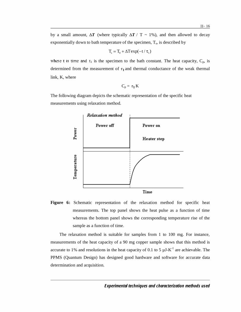
16
Experimental techniques and characterization methods used
by a small amount, T∆ (where typically T∆ / T ~ 1%), and then allowed to decay
exponentially down to bath temperature of the specimen, Ts, is described by
T T T ts = + −0 1∆ exp( / )τ
1 is the specimen to the bath constant. The heat capacity, Cp, is
determined from the measurement of 1τ and thermal conductance of the weak thermal
link, K, where
Cp = 1τ K
The following diagram depicts the schematic representation of the specific heat
measurements using relaxation method.
Figure 6: Schematic representation of the relaxation method for specific heat
measurements. The top panel shows the heat pulse as a function of time
whereas the bottom panel shows the corresponding temperature rise of the
sample as a function of time.
The relaxation method is suitable for samples from 1 to 100 mg. For instance,
measurements of the heat capacity of a 90 mg copper sample shows that this method is
accurate to 1% and resolutions in the heat capacity of 0.1 to 5 µJ-K-1 are achievable. The
PPMS (Quantum Design) has designed good hardware and software for accurate data
determination and acquisition.

17
Experimental techniques and characterization methods used
The other popular method for specific heat measurements is the semi-adiabatic
method. The adiabatic calorimetry of speicifc heat measurement uses the classical
definition of specific heat, Cp,
0T where,/ →∆
∆∆= M
T
QC
Pp
where ∆Q is a heat energy pulse that causes a small temperature rise ∆T in the specimen
of mass M. The pulse heating technique can be traced back to Nerst.
Figure 7: Schematic representation of the adiabatic method for specific heat
measurements. The top panel shows the heat pulse as a function of time (which
is supplied only for a small fraction of time) whereas the bottom panel shows
the corresponding variation of temperature of the sample as a function of time.
In practice the sample is connected to addenda, which consists of the sample
support system. The sample/addenda assembly is thermally insulated from the
surroundings to make the system adiabatic. Thermal equilibrium with the surroundings is
established before and after the heat pulse ∆Q. The temperature, T, is monitored as a
function as a function of time, and the time Ti and Tf at the beginning and end of the heat
pulse are corrected for any heat exchange with the environment of extrapolating T before
and after the heat pulse to the time that corresponds to the midpoint of the pulse. The
18
Experimental techniques and characterization methods used
temperature increment is then ∆T=Tf-Ti, from which Cp is obtained at the temperature
Tm=(Ti-Tf)/2. The adiabatic conditions occur only when there is no heat transfer between
the calorimeter and surrounding shield. After the heat pulse the calorimeter will be at a
temperature slightly above that of shield and there will be a downward drift. Therefore,
the experimental conditions are more appropriately described as being ‘semi-adiabatic’
or ‘quasi-adiabatic’. Owing to this reason, this method is also known as semi-adiabatic
method.
During the course of present study in this thesis, we have employed relaxation
method for specific measurements using a Physical Property Measurement Systems
(PPMS), Quantum Design at TIFR, Mumbai.

19
Experimental techniques and characterization methods used
REFERENCES
1. E. M. Engler, Chem. Technol. 17 (1987) 542.
2. S.X. Dou, H.K. Liu, A.J. Bourdillon, J.P. Zhou, N.X. Tan, X.Y. Sun, C.C.
Sorrell, J. Am. Ceram. Soc., 71C, 329 (1998)
3. C.J. Brinkered and G.W. Scherer, “Sol-Gel Science” Academic Press Inc,
Boston (1990).
4. T. Venkatesan, X.D. Wu, R. Muenchausen and A. Pique, MRS Bull. 17
(1992) 54.
5. S.P. Gapanov, B.M. Luskin, N.N. Salaschenko, Sov. Tech. Phys. Lett. 5, 210
(1979).
6. S.P. Gapanov, A. Gudkov, A.A. Fraerman, Sov. Tech. Phys. Lett. 27, 1130
(1982).
7. D. Basting, K. Mohla, E. Albers, M.V. Bergman, Lases & Optoelektronik, 2,
128 (1984).
8. B.D. Culity, “X-Ray Diffraction”, Addison-Wesly Pub. Co. Inc. (1978).
9. A. Taylor, “X-ray Metallography”, John Wiley & Sons (1961).
10. A.R. West, Solid State Chemistry and its Applications, John Wiley & Sons,
Chichester (1984).
11. H. M. Rietveld, J. Appl. Cryst. 2 (1969) 65.
12. R.A. Young, The Rietveld Method, Oxford University Press Inc, New York,
1993.
13. G. Binning, C.F. Quate and Ch. Gerber, Phys. Rev. Lett. 56, 930 (1986).
14. G. Binning, H. Rohrer, Rev. Mod. Phys. 71, S324 (1999).
15. T.R. Albrecht, P. Grutter, D. Horne, D. Rugar, J. Appl. Phys. 69, 668 (1991).
16. L. J. Vanderpauw, Philips Res. Repts. 16, 187 (1961).
17. SQUID Magnetometer, Manual by Quantum Design.
18. Heat Capacity…by S.J. Collocott, in “Specific heat and measurement
Techniques” John Wily and Sons (1999).
19. PPMS manual by Quantum Design.

20
Experimental techniques and characterization methods used
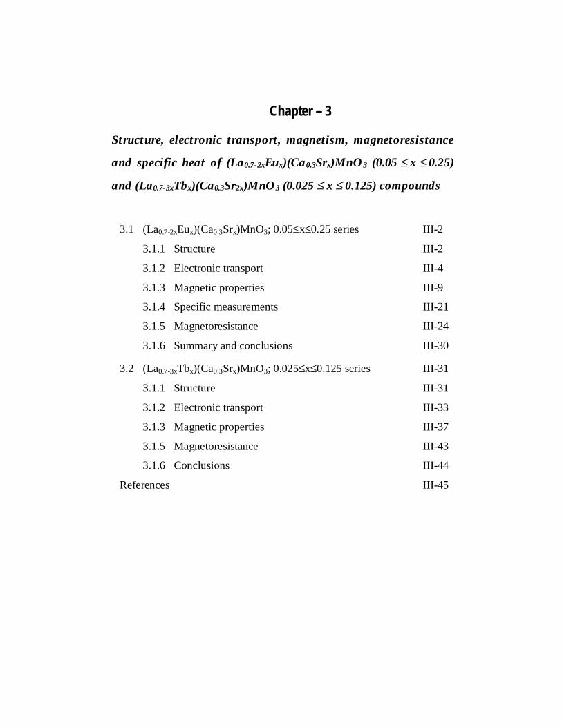
Chapter – 3
Structure, electronic transport, magnetism, magnetoresistance
and specific heat of (La0.7-2xEux)(Ca0.3Srx)MnO3 (0.05 ≤ x ≤ 0.25)
and (La0.7-3xTbx)(Ca0.3Sr2x)MnO3 (0.025 ≤ x ≤ 0.125) compounds
3.1 (La0.7-2xEux)(Ca0.3Srx)MnO3; 0.05≤x≤0.25 series III-2
3.1.1 Structure III-2
3.1.2 Electronic transport III-4
3.1.3 Magnetic properties III-9
3.1.4 Specific measurements III-21
3.1.5 Magnetoresistance III-24
3.1.6 Summary and conclusions III-30
3.2 (La0.7-3xTbx)(Ca0.3Srx)MnO3; 0.025≤x≤0.125 series III-31
3.1.1 Structure III-31
3.1.2 Electronic transport III-33
3.1.3 Magnetic properties III-37
3.1.5 Magnetoresistance III-43
3.1.6 Conclusions III-44
References III-45

1
Structure, electronic transport, magnetism………………………compounds
It is well established that insulator-metal (I-M) transition and paramagnetic-
ferromagnetic transition temperatures (Tp and TC, respectively) of the manganite
perovskites are controlled by three factors, namely, i) the Goldschmidt tolerance factor,
ii) the carrier density determined by the amount of hole doping and iii) size variance
(σ2), given by the relation, σ2 = Σxiri2 - <rA>2 [1-6]. The effect of size disorder on TC and
Tp for fixed average <rA> with optimal hole doping has been investigated by Martinez et
al., who found that with increasing size variance, the Curie temperature falls
monotonically with a corresponding fall in CMR effect [7-8]. The effect of size disorder
on charge-ordering temperature (TCO) and Néel temperature (TN) for charge-exchange
(CE) type charge-ordered (CO) state (fixed <rA> of 1.17 Å and 1.24 Å) has been studied
[9]. These authors showed that, there is no effect on TCO and TN due to increasing size-
disorder. In contrast to these results, it has been reported that increasing disorder of A-
site cations suppresses TN in charge-ordered systems [10,11]. Also, a large mismatch in
the size of A-site cations results in a random arrangement of Mn3+ and Mn4+ ions.
Although the effects of increase in size disorder and carrier density have been
studied, it would be interesting to study the simultaneous substitution of a smaller size
trivalent heavy rare earth cation, along with a larger size divalent cation in
La0.7Ca0.3MnO3 (LCMO) [2] system. In this context, an effort has been made to study the
effect of increasing size disorder and carrier density on the electronic and magnetic
properties in going from optimally-doped to half-doped LCMO system. With this aim,
we have synthesized (La0.7-2xEux)(Ca0.3Srx)MnO3 (0.05≤x≤0.25) and
(La0.7-3xTbx)(Ca0.3Sr2x)MnO3 (0.025≤x≤0.125) compositions and studied their various
physical properties. In this system, the size variance increases with increasing doping
content. The cations Eu3+ (1.12Å) and Sr2+ (1.31Å) in (La0.7-2xEux)(Ca0.3Srx)MnO3;
0.05≤x≤0.25 are best suited for this kind of study because their simultaneous substitution
has no effect on the average A-site cation radius which is fixed at <rA>=1.205Å for all
the compositions. Similarly, (La0.7-3xTbx)(Ca0.3Sr2x)MnO3 (0.025≤ x ≤ 0.125) series is
best suited for the present study because co-substitution of Tb3+ (1.09Å) and Sr2+ (1.31Å)
does not change the average A-site cation radius which is fixed at <rA>=1.207Å for all
the compositions
2
Structure, electronic transport, magnetism………………………compounds
Polycrystalline samples of (La0.7-2xEux)(Ca0.3Srx)MnO3 with x=0.05, 0.1, 0.15, 0.2
and 0.25 and (La0.7-3xTbx)(Ca0.3Sr2x)MnO3 with x = 0.025, 0.05, 0.075, 0.1, 0.125 were
synthesized using the conventional solid state reaction route. The dried forms of La2O3,
Eu2O3, Tb2O3, CaCO3, SrCO3 and MnO2 (purity> 99.9%) were mixed in stoichiometric
proportions and calcined at 950°C for 24 hours. The samples were then pressed into
pellets and sintered at 1100ºC for 30 hrs followed by a sintering at 1200ºC for 100 hrs
with intermediate grindings. The final sintering was carried out at 1350ºC for 24 hrs for
better crystallization. The XRD patterns were recorded on a SIEMENS diffractometer
using Cu-Kα radiation. Electrical resistivity measurements as a function of temperature
in range 5K-320K and as a function of magnetic field up to 9 Tesla were performed
using d.c. four-probe method (PPMS, Quantum Design). Similarly, magnetization data
were acquired as a function of temperature in a range 5K-330K and magnetic field up to
9 Tesla on a SQUID magnetometer (MPMS) and PPMS at TIFR, Mumbai. Heat capacity
as a function of temperature and magnetic field was measured using relaxation method
(PPMS).
3.1 (La0.7-2xEux)(Ca0.3Srx)MnO3; 0.05≤x≤0.25 series
3.1.1 Structure
Powder x-ray diffraction studies showed that (La0.7-2xEux)(Ca0.3Srx)MnO3
(0.05≤x≤0.25) samples are single phase materials with no detectable impurities within
the XRD limit. Structural refinement was carried out by Rietveld fitting of XRD patterns
using standard FULLPROF program [12]. XRD data for all the samples fit to an O′ type
distorted orthorhombic structure (space group - Pnma, no. 62, c>a>b/√2). Fig. 1(a)
shows the XRD patterns of all the samples and the fig. 1(b) displays a typical Rietveld
fitted XRD pattern. The refined cell parameters given in Table-I are found to decrease
with increasing doping concentrations of Eu and Sr. The size variance increases with
increasing x but the average cation radius remains constant throughout the doping range.
The decrease in the cell parameters with increasing x, in spite of constant <rA>, may be
attributed to the increasing Mn4+ content and the lattice distortion caused by the random
displacement of oxygen ions [9].
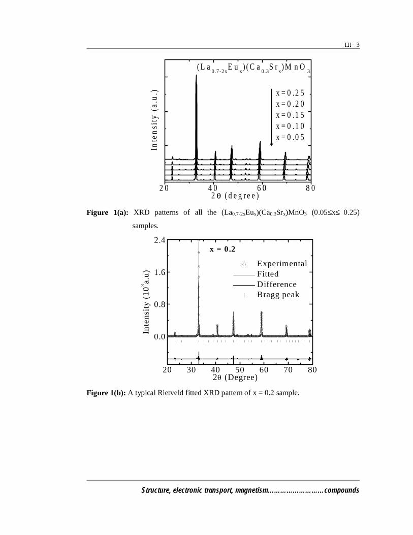
3
Structure, electronic transport, magnetism………………………compounds
2 0 4 0 6 0 8 0
( L a0.7-2x
E ux) ( C a
0.3S r
x) M n O
3
Inte
nsi
ty (
a.u
.)
2 θ ( d e g r e e )
x = 0 .2 5x = 0 .2 0x = 0 .1 5x = 0 .1 0x = 0 .0 5
Figure 1(a): XRD patterns of all the (La0.7-2xEux)(Ca0.3Srx)MnO3 (0.05≤x≤ 0.25)
samples.
20 30 40 50 60 70 80
0.0
0.8
1.6
2.4x = 0.2
Inte
nsit
y (1
03 a.u)
2θ (Degree)
Experimental Fitted Difference Bragg peak
Figure 1(b): A typical Rietveld fitted XRD pattern of x = 0.2 sample.
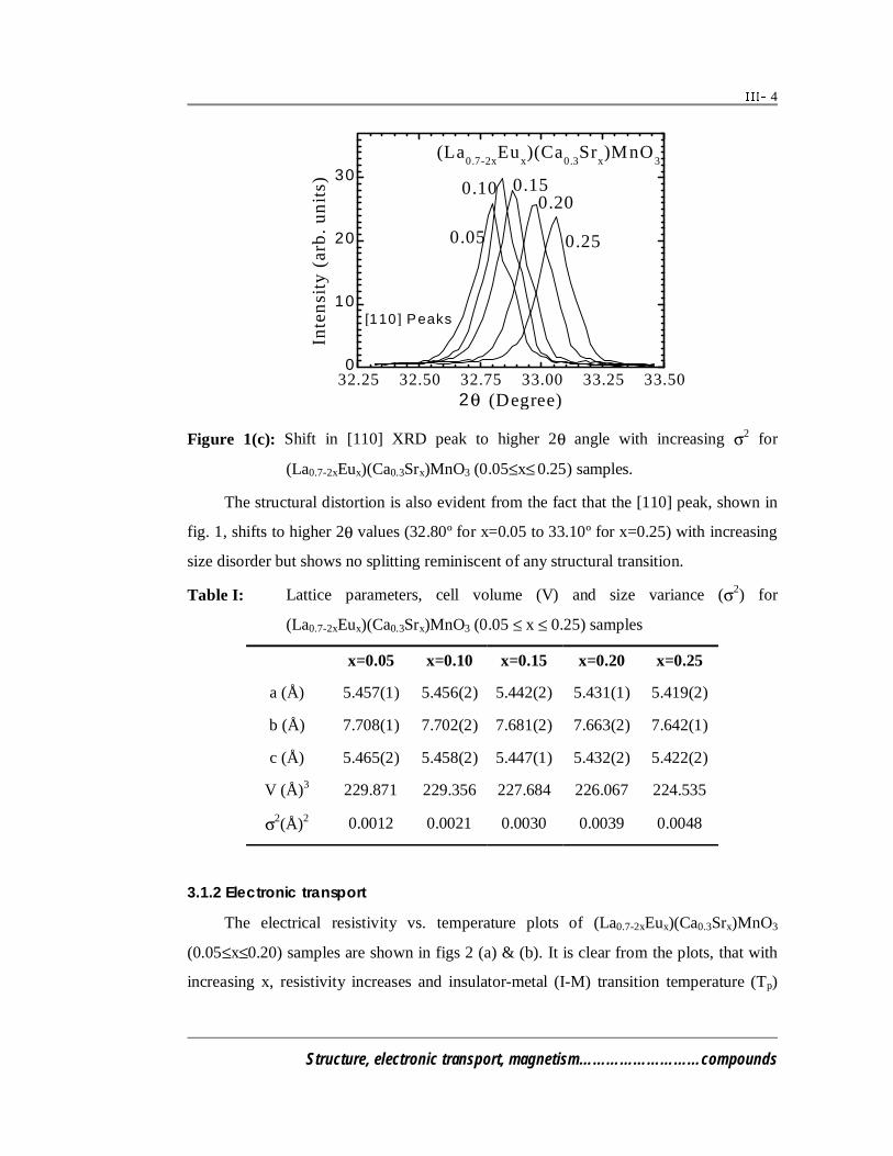
4
Structure, electronic transport, magnetism………………………compounds
32.25 32.50 32.75 33.00 33.25 33.500
10
20
30(La
0.7-2xEu
x)(Ca
0.3Sr
x)MnO
3
0.05
0.10 0.150.20
0.25
[110 ] PeaksIn
ten
sity
(ar
b.
unit
s)
2θ (Degree)
Figure 1(c): Shift in [110] XRD peak to higher 2θ angle with increasing σ2 for
(La0.7-2xEux)(Ca0.3Srx)MnO3 (0.05≤x≤ 0.25) samples.
The structural distortion is also evident from the fact that the [110] peak, shown in
fig. 1, shifts to higher 2θ values (32.80º for x=0.05 to 33.10º for x=0.25) with increasing
size disorder but shows no splitting reminiscent of any structural transition.
Table I: Lattice parameters, cell volume (V) and size variance (σ2) for
(La0.7-2xEux)(Ca0.3Srx)MnO3 (0.05 ≤ x ≤ 0.25) samples
x=0.05 x=0.10 x=0.15 x=0.20 x=0.25
a (Å) 5.457(1) 5.456(2) 5.442(2) 5.431(1) 5.419(2)
b (Å) 7.708(1) 7.702(2) 7.681(2) 7.663(2) 7.642(1)
c (Å) 5.465(2) 5.458(2) 5.447(1) 5.432(2) 5.422(2)
V (Å)3 229.871 229.356 227.684 226.067 224.535
σ2(Å)2 0.0012 0.0021 0.0030 0.0039 0.0048
3.1.2 Electronic transport
The electrical resistivity vs. temperature plots of (La0.7-2xEux)(Ca0.3Srx)MnO3
(0.05≤x≤0.20) samples are shown in figs 2 (a) & (b). It is clear from the plots, that with
increasing x, resistivity increases and insulator-metal (I-M) transition temperature (Tp)
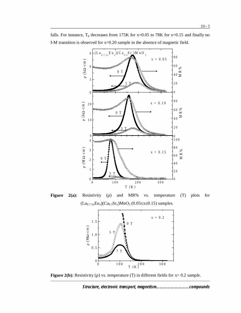
5
Structure, electronic transport, magnetism………………………compounds
falls. For instance, Tp decreases from 175K for x=0.05 to 78K for x=0.15 and finally no
I-M transition is observed for x=0.20 sample in the absence of magnetic field.
0
1 0
2 0
0 T
5 T
0 T
x = 0 . 1 0
( L a0 . 7 - 2 x
E ux) ( C a
0 . 3S r
x) M n O
3
0
3
6
9
MR
%M
R%
ρ (
k Ω-c
m)
T ( K )
5 T
0 T
MR
%
x = 0 . 0 5
ρ (
k Ω-c
m)
0 1 0 0 2 0 0 3 0 00
1
2
3
4
5 T
x = 0 . 1 5
ρ (
MΩ
-cm
)
0
2 0
4 0
6 0
8 0
0
2 0
4 0
6 0
8 0
0
2 0
4 0
6 0
8 0
1 0 0
Figure 2(a): Resistivity (ρ) and MR% vs. temperature (T) plots for
(La0.7-2xEux)(Ca0.3Srx)MnO3 (0.05≤x≤0.15) samples.
0 1 0 0 2 0 0 3 0 00
0 .5
1 .0
1 .5x = 0 .2
7 T
5 T
0 T
ρ (
MΩ
-cm
)
T ( K )
Figure 2(b): Resistivity (ρ) vs. temperature (T) in different fields for x= 0.2 sample.
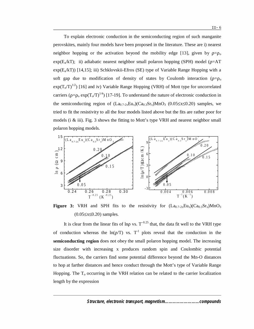
6
Structure, electronic transport, magnetism………………………compounds
To explain electronic conduction in the semiconducting region of such manganite
perovskites, mainly four models have been proposed in the literature. These are i) nearest
neighbor hopping or the activation beyond the mobility edge [13], given by ρ=ρo
exp(Ea/kT); ii) adiabatic nearest neighbor small polaron hopping (SPH) model (ρ=AT
exp(Ea/kT)) [14,15]; iii) Schklovskii-Efros (SE) type of Variable Range Hopping with a
soft gap due to modification of density of states by Coulomb interaction (ρ=ρo
exp(To/T)1/2) [16] and iv) Variable Range Hopping (VRH) of Mott type for uncorrelated
carriers (ρ=ρo exp(To/T)1/4) [17-19]. To understand the nature of electronic conduction in
the semiconducting region of (La0.7-2xEux)(Ca0.3Srx)MnO3 (0.05≤x≤0.20) samples, we
tried to fit the resistivity to all the four models listed above but the fits are rather poor for
models (i & iii). Fig. 3 shows the fitting to Mott’s type VRH and nearest neighbor small
polaron hopping models.
0 .2 4 0 .2 6 0 .2 8 0 .3 0
3
6
9
1 2
1 5( L a
0.7-2xE u
x) ( C a
0.3S r
x) M n O
3
0 . 0 5
0 . 1 00 . 2 0
0 . 1 5
ln ρ
(Ω
cm
)
T- 0 . 2 5
( K- 0 . 2 5
) 0 .0 0 4 0 .0 0 6 0 .0 0 8
- 3
0
3
6
9
0 .0 5
0 .1 50 .1 0
0 .2 0
( L a0 . 7 - 2 x
E ux) ( C a
0 . 3S r
x) M n O
3ln
( ρ/T
)(Ω
cm
/K)
T - 1 ( K - 1 )
Figure 3: VRH and SPH fits to the resistivity for (La0.7-2xEux)(Ca0.3Srx)MnO3
(0.05≤x≤0.20) samples.
It is clear from the linear fits of lnρ vs. T–0.25 that, the data fit well to the VRH type
of conduction whereas the ln(ρ/T) vs. T-1 plots reveal that the conduction in the
semiconducting region does not obey the small polaron hopping model. The increasing
size disorder with increasing x produces random spin and Coulombic potential
fluctuations. So, the carriers find some potential difference beyond the Mn-O distances
to hop at farther distances and hence conduct through the Mott’s type of Variable Range
Hopping. The To occurring in the VRH relation can be related to the carrier localization
length by the expression
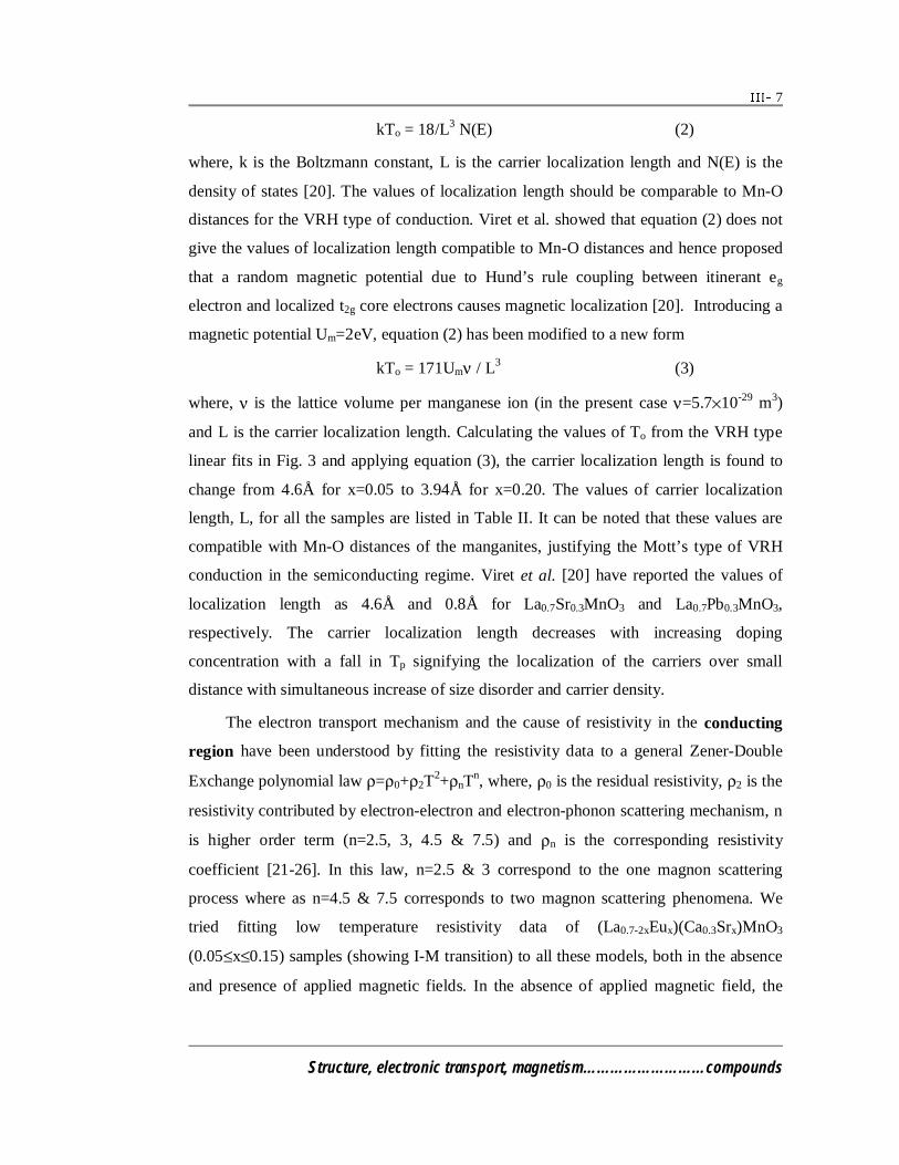
7
Structure, electronic transport, magnetism………………………compounds
kTo = 18/L3 N(E) (2)
where, k is the Boltzmann constant, L is the carrier localization length and N(E) is the
density of states [20]. The values of localization length should be comparable to Mn-O
distances for the VRH type of conduction. Viret et al. showed that equation (2) does not
give the values of localization length compatible to Mn-O distances and hence proposed
that a random magnetic potential due to Hund’s rule coupling between itinerant eg
electron and localized t2g core electrons causes magnetic localization [20]. Introducing a
magnetic potential Um=2eV, equation (2) has been modified to a new form
kTo = 171Umν / L3 (3)
where, ν is the lattice volume per manganese ion (in the present case ν=5.7×10⁻²⁹ m3)
and L is the carrier localization length. Calculating the values of To from the VRH type
linear fits in Fig. 3 and applying equation (3), the carrier localization length is found to
change from 4.6Å for x=0.05 to 3.94Å for x=0.20. The values of carrier localization
length, L, for all the samples are listed in Table II. It can be noted that these values are
compatible with Mn-O distances of the manganites, justifying the Mott’s type of VRH
conduction in the semiconducting regime. Viret et al. [20] have reported the values of
localization length as 4.6Å and 0.8Å for La0.7Sr0.3MnO3 and La0.7Pb0.3MnO3,
respectively. The carrier localization length decreases with increasing doping
concentration with a fall in Tp signifying the localization of the carriers over small
distance with simultaneous increase of size disorder and carrier density.
The electron transport mechanism and the cause of resistivity in the conducting
region have been understood by fitting the resistivity data to a general Zener-Double
Exchange polynomial law ρ=ρ0+ρ2T2+ρnT
n, where, ρ0 is the residual resistivity, ρ2 is the
resistivity contributed by electron-electron and electron-phonon scattering mechanism, n
is higher order term (n=2.5, 3, 4.5 & 7.5) and ρn is the corresponding resistivity
coefficient [21-26]. In this law, n=2.5 & 3 correspond to the one magnon scattering
process where as n=4.5 & 7.5 corresponds to two magnon scattering phenomena. We
tried fitting low temperature resistivity data of (La0.7-2xEux)(Ca0.3Srx)MnO3
(0.05≤x≤0.15) samples (showing I-M transition) to all these models, both in the absence
and presence of applied magnetic fields. In the absence of applied magnetic field, the
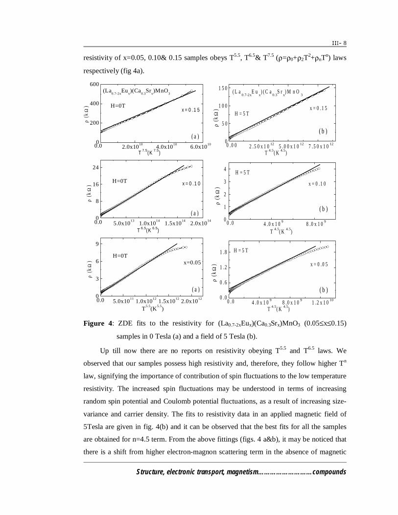
8
Structure, electronic transport, magnetism………………………compounds
resistivity of x=0.05, 0.10& 0.15 samples obeys T5.5, T6.5& T7.5 (ρ=ρ0+ρ2T2+ρnT
n) laws
respectively (fig 4a).
0.0 5.0x10¹¹
1.0x10¹²
1.5x10¹²
2.0x10120
3
6
9
( a )
H=0T
ρ (
kΩ
)
x=0.05
ρ (
kΩ
)
T5.5
(K5.5
)
0.0 5.0x10¹³
1.0x10¹⁴
1.5x10¹⁴
2.0x10140
8
16
24
( a )
H=0T
x = 0 .1 0
T 6.5(K 6.5)
0.0 2.0x10¹⁰
4.0x10¹⁰
6.0x10100
200
400
600
( a )
H=0T
(La0.7-2x
Eux)(Ca
0.3Sr
x)MnO
3
ρ
(k
Ω)
T 7.5(K 7.5)
x = 0 .1 5
0 .0 4 .0 x 1 0 9 8 .0 x 1 0 9 1 .2 x 1 0 100 .0
0 .6
1 .2
1 .8
( b )
H = 5 T
x = 0 .0 5
ρ (
kΩ
)
T 4.5( K 4.5)
0 .0 4 .0 x 1 0 9 8 .0 x 1 0 90
1
2
3
4
( b )
H = 5 T
T4.5
( K4.5
)
x = 0 .1 0
ρ (
kΩ
)
0 .0 0 2 .5 0 x 1 0 12 5 .0 0 x 1 0 12 7 .5 0 x 1 0 120
5 0
1 0 0
1 5 0
( b )
( L a0.7-2x
E ux) ( C a
0.3S r
x) M n O
3
H = 5 T
T 4.5( K 4.5)
ρ (
kΩ
) x = 0 .1 5
Figure 4: ZDE fits to the resistivity for (La0.7-2xEux)(Ca0.3Srx)MnO3 (0.05≤x≤0.15)
samples in 0 Tesla (a) and a field of 5 Tesla (b).
Up till now there are no reports on resistivity obeying T5.5 and T6.5 laws. We
observed that our samples possess high resistivity and, therefore, they follow higher Tn
law, signifying the importance of contribution of spin fluctuations to the low temperature
resistivity. The increased spin fluctuations may be understood in terms of increasing
random spin potential and Coulomb potential fluctuations, as a result of increasing size-
variance and carrier density. The fits to resistivity data in an applied magnetic field of
5Tesla are given in fig. 4(b) and it can be observed that the best fits for all the samples
are obtained for n=4.5 term. From the above fittings (figs. 4 a&b), it may be noticed that
there is a shift from higher electron-magnon scattering term in the absence of magnetic

9
Structure, electronic transport, magnetism………………………compounds
field to lower electron-magnon scattering terms in applied field of 5T. These points
towards the field-induced suppression of spin fluctuations.
3.1.2 Magnetic properties
We have carried out zero-field-cooled (ZFC) and field-cooled (FC) magnetization
(M) measurements on (La0.7-2xEux)(Ca0.3Srx)MnO3 (0.05≤x≤0.25) samples in an applied
field of 50 Oe and temperature range of 5K-330K.
0 1 0 0 2 0 0 3 0 00
2
4
6
8
1 0
1 2
H = 5 0 O e
( a )
( L a0 . 7 - 2 x
E ux) ( C a
0 . 3S r
x) M n O
3
0 .0 5
0 .1 0
0 .1 5
M (
em
u/g
m)
T (K )
0 1 0 0 2 0 0 3 0 00 .0
0 .4
0 .8
1 .2
1 .6
2 .0
H = 5 0 O e
( L a0 . 7 - 2 x
E ux) ( C a
0 . 3S r
x) M n O
3
0 .2 0
0 .2 5 M (
em
u/g
m)
T (K )
M (
em
u/g
m)
0 .0 0
0 .0 2
0 .0 4
0 .0 6
0 .0 8
0 .1 0
0 .1 2
( b )
Figure 5(a&b): Zero-field-cooled and field cooled magnetization versus temperature
plots for (La0.7-2xEux)(Ca0.3Srx)MnO3(0.05≤x≤0.25) samples.
As shown in figs. 5 (a&b), the TC (taken as the branching temperature of MZFC(T)
and MFC(T)) falls from 200K for x=0.05 to 75K for x=0.20. The large drop in TC may be
attributed to increasing size disorder, which results in the random displacement of
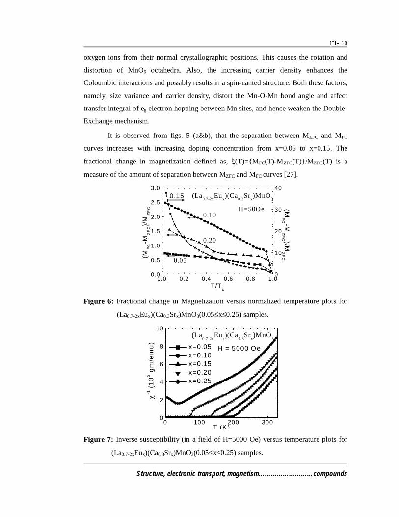
10
Structure, electronic transport, magnetism………………………compounds
oxygen ions from their normal crystallographic positions. This causes the rotation and
distortion of MnO6 octahedra. Also, the increasing carrier density enhances the
Coloumbic interactions and possibly results in a spin-canted structure. Both these factors,
namely, size variance and carrier density, distort the Mn-O-Mn bond angle and affect
transfer integral of eg electron hopping between Mn sites, and hence weaken the Double-
Exchange mechanism.
It is observed from figs. 5 (a&b), that the separation between MZFC and MFC
curves increases with increasing doping concentration from x=0.05 to x=0.15. The
fractional change in magnetization defined as, ξ(T)=MFC(T)-MZFC(T)/MZFC(T) is a
measure of the amount of separation between MZFC and MFC curves [27].
0.0 0.2 0.4 0.6 0.8 1.00.0
0.5
1.0
1.5
2.0
2.5
3.0
0
10
20
30
40(La
0.7-2xEu
x)(Ca
0.3Sr
x)MnO
3
0.20
0.05
0.10
0 .15
(MF
C-M
ZF
C)/
MZ
FC (M
FC -M
ZF
C )/MZ
FC
T/Tc
H=50Oe
Figure 6: Fractional change in Magnetization versus normalized temperature plots for
(La0.7-2xEux)(Ca0.3Srx)MnO3(0.05≤x≤0.25) samples.
0 100 200 3000
2
4
6
8
10(La
0.7-2xEu
x)(Ca
0.3Sr
x)MnO
3
H = 5000 Oe
χ-1
(1
03 g
m/e
mu
)
T (K)
x=0.05 x=0.10 x=0.15 x=0.20 x=0.25
Figure 7: Inverse susceptibility (in a field of H=5000 Oe) versus temperature plots for
(La0.7-2xEux)(Ca0.3Srx)MnO3(0.05≤x≤0.25) samples.

11
Structure, electronic transport, magnetism………………………compounds
Fig. 6 shows the plots of ξ(T) vs. T/TC. It is clear from the figure that the field-
cooled magnetization (MFC) increases more rapidly at low temperatures as x increases.
The origin of increasing magnetization may be attributed to the magnetic field induced
suppression of spin fluctuations, which arise from increasing size disorder and Mn4+
content. We have also carried out MZFC measurements in an applied field of 5000 Oe.
The inverse susceptibility vs. temperature, T, plots are shown in Fig. 7. The
susceptibility of all the compositions does not obey Curie-Weiss law and the deviation
from the Curie-Weiss behavior increases with increasing doping concentration. This can
be attributed to the presence of magnetic inhomogeneities in the paramagnetic region
and, therefore, the absence of long-range magnetic order.
Magnetization (M) vs. field (H) isotherms were recorded on
(La0.7-2xEux)(Ca0.3Srx)MnO3 (0.05≤x≤0.20) samples up to a field of 5 Tesla at 5K and
300K. As expected, saturation in magnetization is not observed in the paramagnetic
region at 300K. However, at 5K, all the samples show a saturation magnetization up to a
field of 5 Tesla. Fig. 8 shows M vs. H plots for the samples studied from which it is clear
that there are no magnetic hysteresis effects for any composition except x=0.20. The
theoretical values of saturation magnetization (MS) are calculated from the spin only
values of Mn ions using the standard relation MS=gµBS, where g and µB have their usual
meanings and S is the average spin value of Mn3+ (S=2) and Mn4+ ions (S=3/2). From
Table II, it is seen that the calculated values of saturation magnetization (MS) are in good
agreement with the experimentally observed values.
Table II: Curie temperature (TC), insulator-metal transition (Tp), localization length (L),
theoretically calculated and experimentally observed saturation magnetization
(MS) values of La0.7-2xEuxCa0.3SrxMnO3 (0.05 ≤ x ≤ 0.25) samples
X TC (K) Tp (K) L () B (calculated) B (experimental)
0.05 195 175 4.60 3.65 3.63
0.10 173 158 4.35 3.60 3.58
0.15 130 78 4.05 3.55 3.35
0.20 75 - 3.94 3.50 3.57
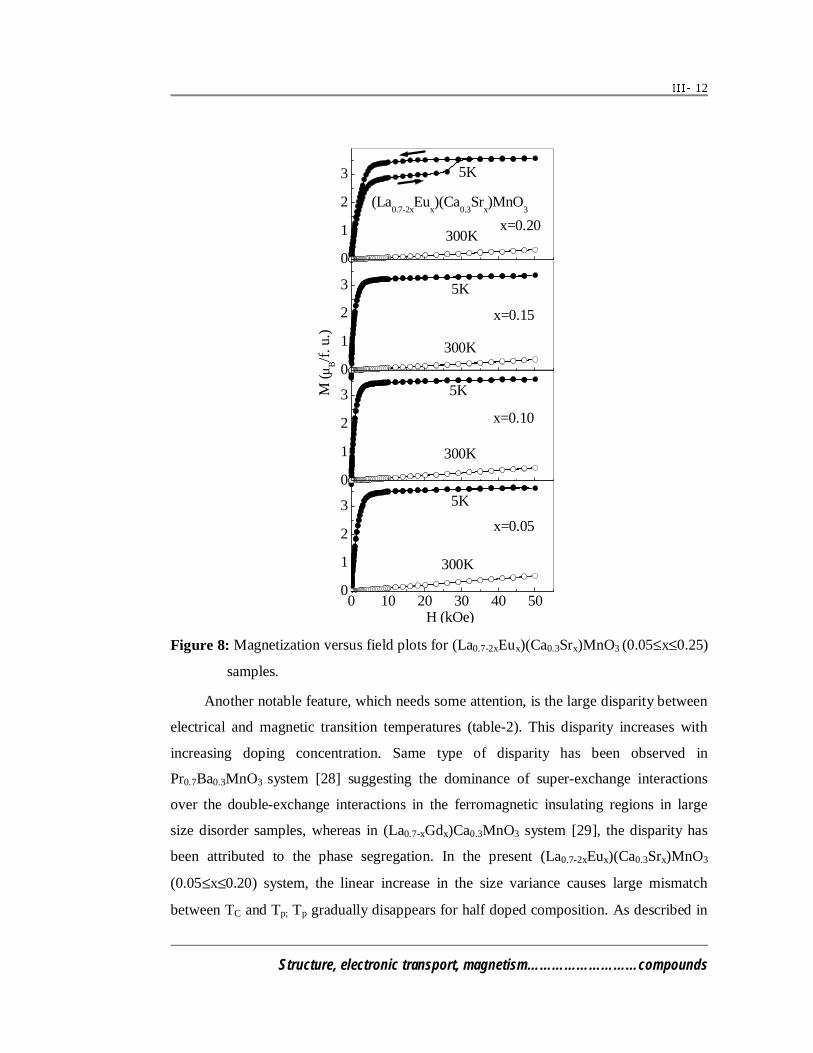
12
Structure, electronic transport, magnetism………………………compounds
0 10 20 30 40 500
1
2
3
5K
300K
x=0.05
H (kOe)
0
1
2
3 5K
300K
x=0.10
M ( µ
B/f
. u.)
0
1
2
3
5K
300K
x=0.15
0
1
2
3
(La0.7-2x
Eux)(Ca
0.3Sr
x)MnO
3
5K
300Kx=0.20
Figure 8: Magnetization versus field plots for (La0.7-2xEux)(Ca0.3Srx)MnO3 (0.05≤x≤0.25)
samples.
Another notable feature, which needs some attention, is the large disparity between
electrical and magnetic transition temperatures (table-2). This disparity increases with
increasing doping concentration. Same type of disparity has been observed in
Pr0.7Ba0.3MnO3 system [28] suggesting the dominance of super-exchange interactions
over the double-exchange interactions in the ferromagnetic insulating regions in large
size disorder samples, whereas in (La0.7-xGdx)Ca0.3MnO3 system [29], the disparity has
been attributed to the phase segregation. In the present (La0.7-2xEux)(Ca0.3Srx)MnO3
(0.05≤x≤0.20) system, the linear increase in the size variance causes large mismatch
between TC and Tp; Tp gradually disappears for half doped composition. As described in
13
Structure, electronic transport, magnetism………………………compounds
ref. 29, the large size variance results in the formation of small insulating phases like
Eu-Ca/Sr-Mn-O phases within the La-Ca/Sr-Mn-O ferromagnetic metallic matrix. The
resistivity of insulating phases keeps rising even after the onset of TC for the conducting
matrix. It is only after the resistivity of these insulating phases saturates that the metallic
conductivity starts appearing. Hence, the Curie temperature is not accompanied by an
insulator-metal transition temperature.
Metamagnetism in x = 0.2 and 0.25 sample: Role of phase-separation
We introduce a new class of metamagnetic manganite compounds other than Pr-
based manganites. A detailed magnetization measurements have been carried out on
half-doped x=0.2 and electron-doped x=0.25 of (La0.7-2xEux)(Ca0.3Srx)MnO3 series. In
long history of magnetic property investigations in manganites, it is observed for the first
time that, apart from Pr doped samples, Eu doped charge-ordered composition exhibit a
sharp step like metamagentic behavior. Magnetism of the half-doped manganites is a
contemporary area of research because of its correlation with CO and OO properties.
Metamagnetism is one such property exhibited by a few of Pr-based hole-doped charge-
ordered compounds. The low bandwidth systems, Pr0.5Ca0.5MnO3, (having a smaller
tolerance factor) represents a robust charge-ordered and orbital-ordered (OO) state,
which melts at a field of 25 Tesla [30]. Since Pr-based compounds present very stable
CO and OO states [30], the melting of this robust state has been induced by diluting the
Mn sublattice through doping magnetic and non-magnetic ions in a series of related
compounds [31-36]. The melting of the CO state manifests itself in a series of
metamamgetic steps depending upon the magnetic nature of the doped ion. These steps
have been reported to be ultra-sharp at low temperatures. The origin of such behavior lies
in martensitic like avalanches [37] and the Barkhausen effect [38] reported for other
metallic hard magnetic compounds.
Apart from the Pr-based systems, in which metamagnetic behavior is typically seen
when doped at the Mn-site, the above-mentioned behavior has not been observed in any
other hole-doped or electron-doped manganites. Here, we show a sharp metamagnetic
behavior in a Eu-doped manganite samples, namely, half-doped x=0.2 and electron-
doped x=0.25 of (La0.7-2xEux)(Ca0.3Srx)MnO3 series. Quite interestingly, the
metamagnetic behavior observed in these samples is in the absence of any kind of doping
14
Structure, electronic transport, magnetism………………………compounds
at the Mn-site. Also, since the value <rA> = 1.205Å in (La0.7-2xEux)(Ca0.3Srx)MnO3 is
somewhat larger than <rA> = 1.18 Å of conventional Pr-based compounds, the presently
studied Eu-compounds, therefore, form a new class of metamagnetic manganite
compounds.
The data for the magnetization and specific heat isotherms were acquired after
heating the sample to 300 K (well above TC) during the course of the isothermal
measurement to eradicate any hystoretic effects. The results of electrical resistance
versus temperature measurements for the x=0.2 (La0.3Eu0.2)(Ca0.3Sr0.2)MnO3 sample
are shown in fig. 2(b) from which it can be seen that the sample exhibits a charge-
ordered state at a temperature of ~150 K while x=0.25 (La0.2Eu0.25)(Ca0.3Sr0.25)MnO3 is
an insulator (not shown in fig.). The resistance vs. temperature for
(La0.3Eu0.2)(Ca0.3Sr0.2)MnO3 in applied magnetic fields of 5 Tesla and 7 Tesla reveals that
the charge-ordered state melts through an insulator-metal transition at ~110 K. The ZFC
and FC magnetization vs. temperature plot of (La0.3Eu0.2)(Ca0.3Sr0.2)MnO3 shows that TC
occurs at ~75 K. Also, as shown in fig. 7, there is a deviation from Curie-Weiss behavior
at a temperature of around 250 K. We will later discuss various properties in the light of
the coexistence of the FM and AFM phases in the temperature range of approximately
75 K to 2 K.
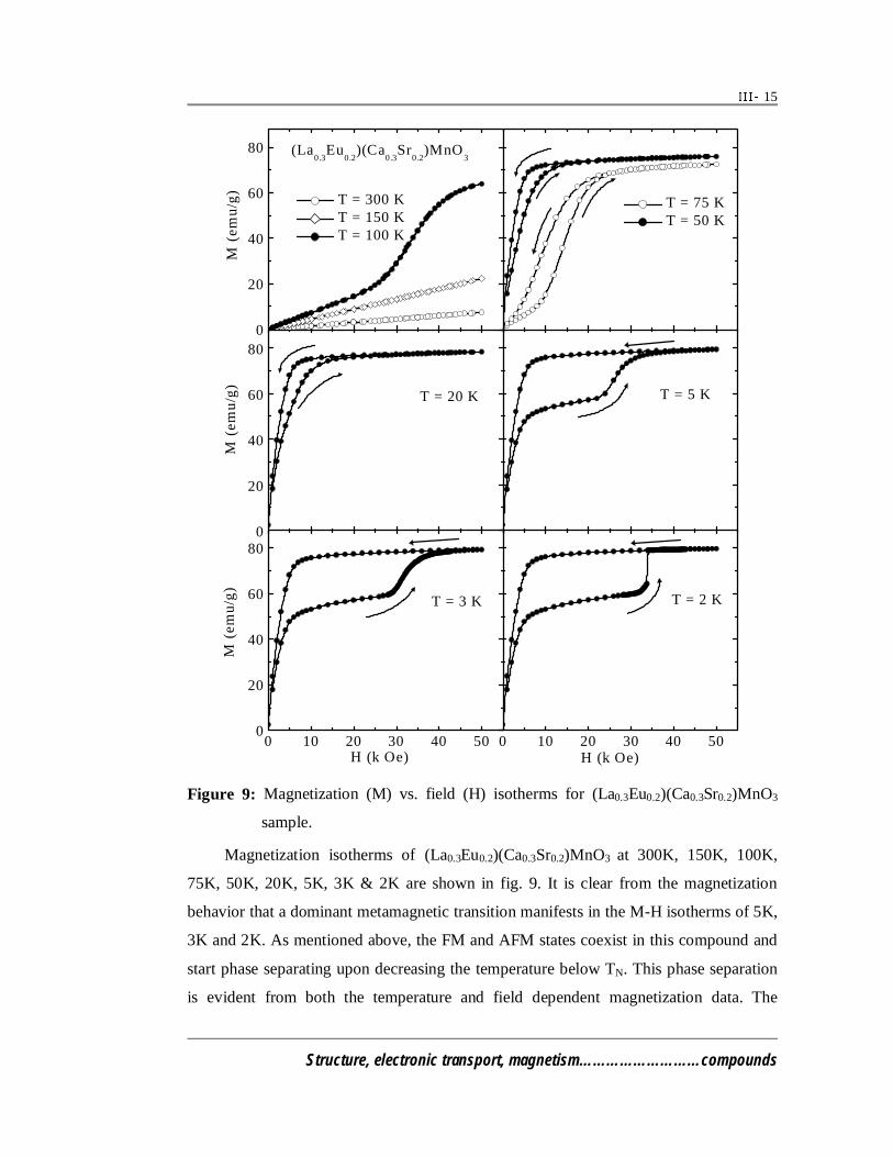
15
Structure, electronic transport, magnetism………………………compounds
0
20
40
60
80
(La0.3
Eu0.2
)(Ca0.3
Sr0.2
)MnO3
T = 300 K T = 150 K T = 100 K
M (
emu/
g)
T = 75 K T = 50 K
0
20
40
60
80
T = 20 K
T = 5 K
0 10 20 30 40 500
20
40
60
80
T = 3 K
M (
emu/
g)M
(em
u/g)
H (k Oe)0 10 20 30 40 50
T = 2 K
H (k Oe)
Figure 9: Magnetization (M) vs. field (H) isotherms for (La0.3Eu0.2)(Ca0.3Sr0.2)MnO3
sample.
Magnetization isotherms of (La0.3Eu0.2)(Ca0.3Sr0.2)MnO3 at 300K, 150K, 100K,
75K, 50K, 20K, 5K, 3K & 2K are shown in fig. 9. It is clear from the magnetization
behavior that a dominant metamagnetic transition manifests in the M-H isotherms of 5K,
3K and 2K. As mentioned above, the FM and AFM states coexist in this compound and
start phase separating upon decreasing the temperature below TN. This phase separation
is evident from both the temperature and field dependent magnetization data. The
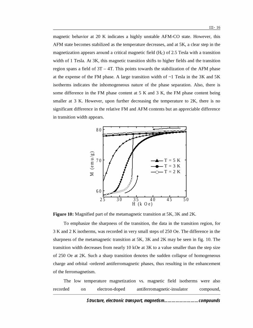
16
Structure, electronic transport, magnetism………………………compounds
magnetic behavior at 20 K indicates a highly unstable AFM-CO state. However, this
AFM state becomes stabilized as the temperature decreases, and at 5K, a clear step in the
magnetization appears around a critical magnetic field (HC) of 2.5 Tesla with a transition
width of 1 Tesla. At 3K, this magnetic transition shifts to higher fields and the transition
region spans a field of 3T – 4T. This points towards the stabilization of the AFM phase
at the expense of the FM phase. A large transition width of ~1 Tesla in the 3K and 5K
isotherms indicates the inhomogeneous nature of the phase separation. Also, there is
some difference in the FM phase content at 5 K and 3 K, the FM phase content being
smaller at 3 K. However, upon further decreasing the temperature to 2K, there is no
significant difference in the relative FM and AFM contents but an appreciable difference
in transition width appears.
2 5 3 0 3 5 4 0 4 5 5 0
6 0
7 0
8 0
M (
emu
/g)
H ( k O e )
T = 5 K T = 3 K T = 2 K
Figure 10: Magnified part of the metamagnetic transition at 5K, 3K and 2K.
To emphasize the sharpness of the transition, the data in the transition region, for
3 K and 2 K isotherms, was recorded in very small steps of 250 Oe. The difference in the
sharpness of the metamagnetic transition at 5K, 3K and 2K may be seen in fig. 10. The
transition width decreases from nearly 10 kOe at 3K to a value smaller than the step size
of 250 Oe at 2K. Such a sharp transition denotes the sudden collapse of homogeneous
charge and orbital -ordered antiferromagnetic phases, thus resulting in the enhancement
of the ferromagnetism.
The low temperature magnetization vs. magnetic field isotherms were also
recorded on electron-doped antiferromagnetic-insulator compound,
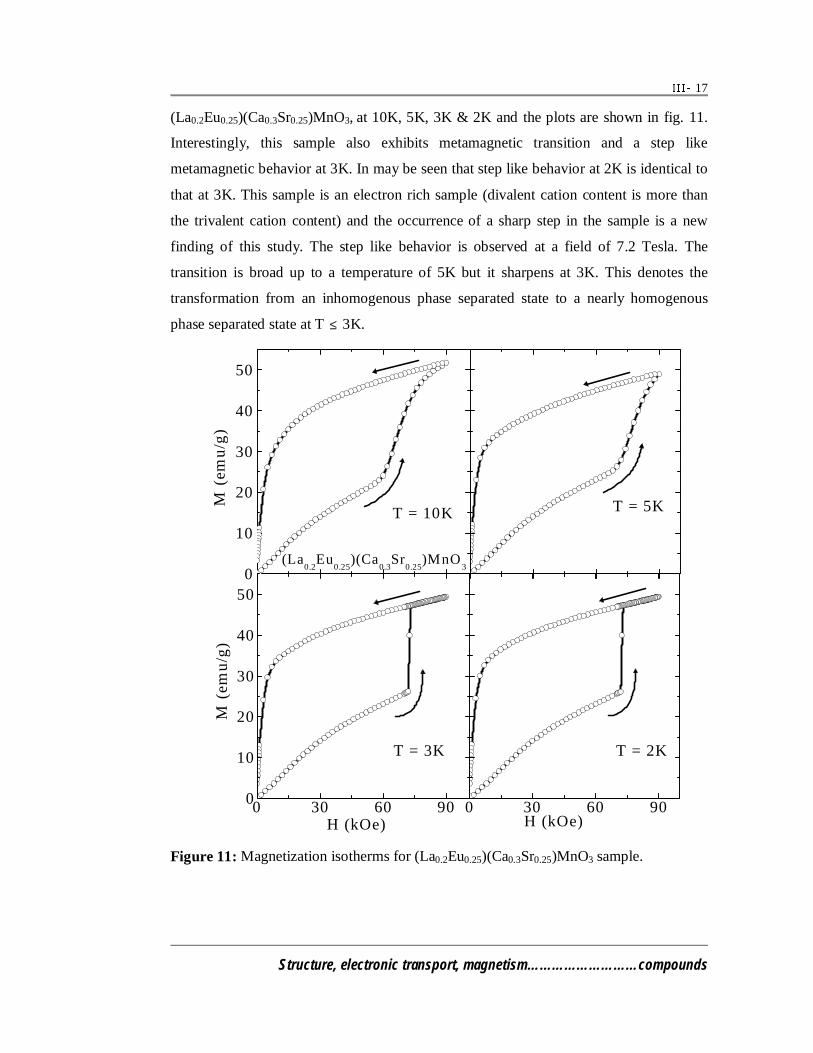
17
Structure, electronic transport, magnetism………………………compounds
(La0.2Eu0.25)(Ca0.3Sr0.25)MnO3, at 10K, 5K, 3K & 2K and the plots are shown in fig. 11.
Interestingly, this sample also exhibits metamagnetic transition and a step like
metamagnetic behavior at 3K. In may be seen that step like behavior at 2K is identical to
that at 3K. This sample is an electron rich sample (divalent cation content is more than
the trivalent cation content) and the occurrence of a sharp step in the sample is a new
finding of this study. The step like behavior is observed at a field of 7.2 Tesla. The
transition is broad up to a temperature of 5K but it sharpens at 3K. This denotes the
transformation from an inhomogenous phase separated state to a nearly homogenous
phase separated state at T ≤ 3K.
0
10
20
30
40
50
T = 10K
(La0.2
Eu0.25
)(Ca0.3
Sr0.25
)MnO3
T = 5K
0 30 60 900
10
20
30
40
50
T = 3K
M (
emu
/g)
H (kOe)
M (
emu
/g)
0 30 60 90
T = 2K
H (kOe)
Figure 11: Magnetization isotherms for (La0.2Eu0.25)(Ca0.3Sr0.25)MnO3 sample.
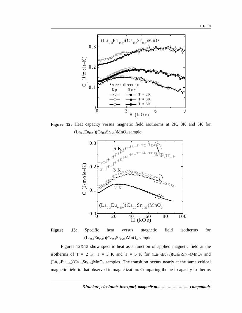
18
Structure, electronic transport, magnetism………………………compounds
0 3 6 90
0 .1
0 .2
0 .3( L a
0.3E u
0.2) ( C a
0.3S r
0.2) M n O
3
Cp (
J/m
ole
-K)
H ( k O e )
S w e e p d i r e c t io n U p D o w n
T = 2 K T = 3 K T = 5 K
Figure 12: Heat capacity versus magnetic field isotherms at 2K, 3K and 5K for
(La0.2Eu0.25)(Ca0.3Sr0.25)MnO3 sample.
0 20 40 60 80 1000.0
0.1
0.2
0.3
2 K
3 K
5 K
(La0.2
Eu0.25
)(Ca0.3
Sr0.25
)MnO3
C (
J/m
ole
-K)
H (kOe)
Figure 13: Specific heat versus magnetic field isotherms for
(La0.2Eu0.25)(Ca0.3Sr0.25)MnO3 sample.
Figures 12&13 show specific heat as a function of applied magnetic field at the
isotherms of T = 2 K, T = 3 K and T = 5 K for (La0.3Eu0.2)(Ca0.3Sr0.2)MnO3 and
(La0.2Eu0.25)(Ca0.3Sr0.25)MnO3 samples. The transition occurs nearly at the same critical
magnetic field to that observed in magnetization. Comparing the heat capacity isotherms
19
Structure, electronic transport, magnetism………………………compounds
of x=0.2 and x=0.25 sample at 5K, it is seen that there is larger change in heat capacity in
transition for x=0.25 sample than x=0.2 sample. This is consistent with the amount of
enhancement in field induced magnetization at the metamagnetic transition. The overall
shape of the C(H) data can be understood in terms of antiferromagnetic and
ferromagnetic spin excitation contributions to the specific heat [39]. A broad irreversible
drop appears in the T = 3 K and T = 5 K measurements at nearly the same critical field as
the metamagnetic transition in the magnetization isotherms. For both the samples, there
is no visible feature in the T = 2 K data corresponding to the step, which is consistent
with the small step in C(H) recently observed in a similar transition in a Pr-based
compound [40]. The absence of a feature at T = 2 K also suggests that the relative
difference in heat capacity between the two magnetoelectronic phases decreases with
decreasing temperature.
It is believed that, in the Mn-site doped Pr based manganites, the defects created by
doping of other cations such as Ga, Cr, Ni, etc. at the Mn-site result in the formation of
FM clusters in the AFM matrix [31-36]. These FM clusters are formed around the doped
ion, thus resulting in a breakdown of the long-range AFM order. Therefore, the
metamagnetic transition in these compounds has been attributed to the melting of AFM
phases to enhance the FM phase content. In the present investigation on
(La0.3Eu0.2)(Ca0.3Sr0.2)MnO3 and (La0.2Eu0.25)(Ca0.2Sr0.25)MnO3, we conjecture that the
coexistence of FM and AFM phases arises in the following way. The large size disorder
results in many intrinsic effects on the crystal structure such as random displacement of
oxygen ions from their actual crystallographic positions [9]. This distorts and rotates the
MnO6 octahedra causing an orbital and spin disorder at the Mn ion sites and breaks the
long-range cooperativity of the Jahn-Teller effect. This phenomenon is well understood
theoretically [41] and proved experimentally [10,11]. Also, it has been reported that as
the size disorder approaches ~0.005Å2, the formation of local hole-rich and electron-rich
incommensurate FM phases and commensurate CO AFM phases takes place [10,11]. In
the present samples under investigation, the separation of the FM and AFM phases starts
at a temperature of ~200 K (evident from deviation in magnetic susceptibility from
Curie-Weiss behavior as shown in fig. 7) when the commensurate phase transforms to an
AFM ground state whereas the other phase becomes ferromagnetic below which FM and
20
Structure, electronic transport, magnetism………………………compounds
AFM phases coexist. Hence, the metamagnetic transition in this sample is a result of a
melting of the AFM phase into a FM phase as the temperature is decreased.
An intriguing aspect of the present study is a large difference in the sharpness of
the metamagnetic step of 250 Oe at 2K as compared to that of 10kOe at 3K for
(La0.3Eu0.2)(Ca0.3Sr0.2)MnO3 [fig. 10]and 500 Oe at 3K as compared to 15kOe at 5K for
(La0.2Eu0.25)(Ca0.2Sr0.25)MnO3 [fig. 11]. In these Eu-based samples, a martensitic like
behavior (invoked for the Pr manganites compounds) may be extended to explain the
origin of such sharpness of the step by considering the structural distortion and magnetic
inhomogeneities in the interfacial regions of the phase separated state. The presence of a
single step in the magnetization and heat capacity of present Eu-based samples, in
contrast to multiple steps in Pr-based compounds [31-36], makes a martensitic like
transition a more plausible cause for such a behavior and may be understood as follows.
The interfacial region of FM and CO AFM phases is magnetically and structurally
inhomogeneous and, therefore, magnetic disorder is more relevant in the AFM phase
However, as the temperature decreases, the moment alignment at these interfacial
regions becomes more of an antiferromagnetic type. As mentioned earlier, at a
temperature where sharp step occurs, the transition (i.e. total conversion to the FM
phase) takes place within a very narrow magnetic step of 500 Oe. Hence, the melting at
2K takes place rapidly when all the moments are flipped simultaneously, whereas at
higher temperatures, the unstable moments flip first and then the avalanche process
starts. This means that, below HC, at 2K a complete ferromagnetic state exists whereas at
3K and 5K, some antiferromagnetic correlations persist up to a field at which complete
saturation is attained. This is an indication of the homogeneous nature of phase
separation at 2K as compared to that at 3K for x=0.2 sample and T ≤ 3K for x=0.25
sample. Hence, this kind of ultra-sharp transition at 2K may be described in analogy to a
martensitic transition.
An unusual feature in the x=0.2 and x=0.25 samples is that the magnetization in
x=0.2 saturates in a field of 50 kOe whereas it does not saturate, in x=0.25, even up to a
field of 90 kOe. The former shows a saturation magnetization of ~3µB vis-à-vis a
theoretical value of 3.5µB (obtained as spin only moments of Mn ions) whereas the latter
attains an experimental magnetization of ~1.9 µB vis-à-vis theoretical ~3.45 µB up to a
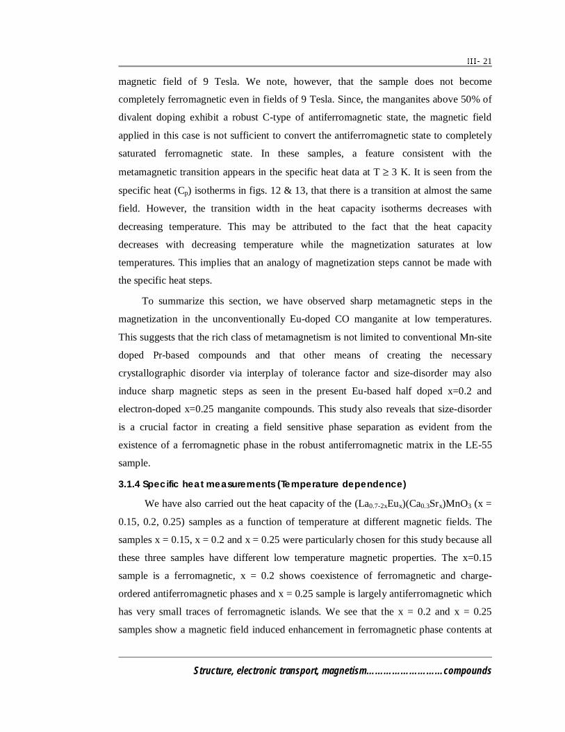
21
Structure, electronic transport, magnetism………………………compounds
magnetic field of 9 Tesla. We note, however, that the sample does not become
completely ferromagnetic even in fields of 9 Tesla. Since, the manganites above 50% of
divalent doping exhibit a robust C-type of antiferromagnetic state, the magnetic field
applied in this case is not sufficient to convert the antiferromagnetic state to completely
saturated ferromagnetic state. In these samples, a feature consistent with the
metamagnetic transition appears in the specific heat data at T ≥ 3 K. It is seen from the
specific heat (Cp) isotherms in figs. 12 & 13, that there is a transition at almost the same
field. However, the transition width in the heat capacity isotherms decreases with
decreasing temperature. This may be attributed to the fact that the heat capacity
decreases with decreasing temperature while the magnetization saturates at low
temperatures. This implies that an analogy of magnetization steps cannot be made with
the specific heat steps.
To summarize this section, we have observed sharp metamagnetic steps in the
magnetization in the unconventionally Eu-doped CO manganite at low temperatures.
This suggests that the rich class of metamagnetism is not limited to conventional Mn-site
doped Pr-based compounds and that other means of creating the necessary
crystallographic disorder via interplay of tolerance factor and size-disorder may also
induce sharp magnetic steps as seen in the present Eu-based half doped x=0.2 and
electron-doped x=0.25 manganite compounds. This study also reveals that size-disorder
is a crucial factor in creating a field sensitive phase separation as evident from the
existence of a ferromagnetic phase in the robust antiferromagnetic matrix in the LE-55
sample.
3.1.4 Specific heat measurements (Temperature dependence)
We have also carried out the heat capacity of the (La0.7-2xEux)(Ca0.3Srx)MnO3 (x =
0.15, 0.2, 0.25) samples as a function of temperature at different magnetic fields. The
samples x = 0.15, x = 0.2 and x = 0.25 were particularly chosen for this study because all
these three samples have different low temperature magnetic properties. The x=0.15
sample is a ferromagnetic, x = 0.2 shows coexistence of ferromagnetic and charge-
ordered antiferromagnetic phases and x = 0.25 sample is largely antiferromagnetic which
has very small traces of ferromagnetic islands. We see that the x = 0.2 and x = 0.25
samples show a magnetic field induced enhancement in ferromagnetic phase contents at
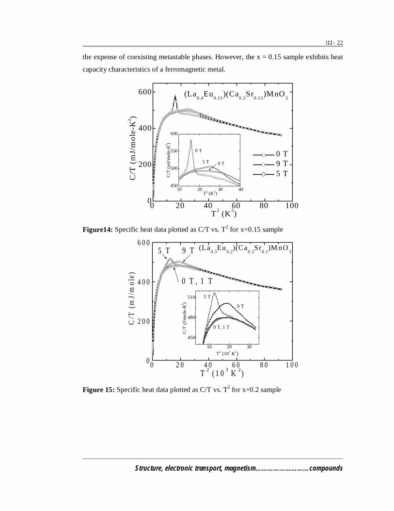
22
Structure, electronic transport, magnetism………………………compounds
the expense of coexisting metastable phases. However, the x = 0.15 sample exhibits heat
capacity characteristics of a ferromagnetic metal.
0 20 40 60 80 1000
200
400
600
10 20 30 40450
500
550
600
9 T
0 T
5 T
C/T
(m
J/m
ole-
K2 )
T2 (K2)
(La0.4
Eu0.15
)(Ca0.3
Sr0.15
)MnO3
C/T
(m
J/m
ole-
K2 )
T2 (K
2)
0 T 9 T 5 T
Figure14: Specific heat data plotted as C/T vs. T2 for x=0.15 sample
0 2 0 4 0 6 0 8 0 1 0 00
2 0 0
4 0 0
6 0 0
10 20 30
450
480
510
0 T, 1 T
9 T
5 T
C/T
(J/
mol
e-K
2 )
T2 (103 K2)
0 T , 1 T
5 T 9 T (La0.3
Eu0.2
)(Ca0.3
Sr0.2
)M nO3
C/T
(m
J/m
ole
)
T 2 ( 1 0 3 K 2)
Figure 15: Specific heat data plotted as C/T vs. T2 for x=0.2 sample
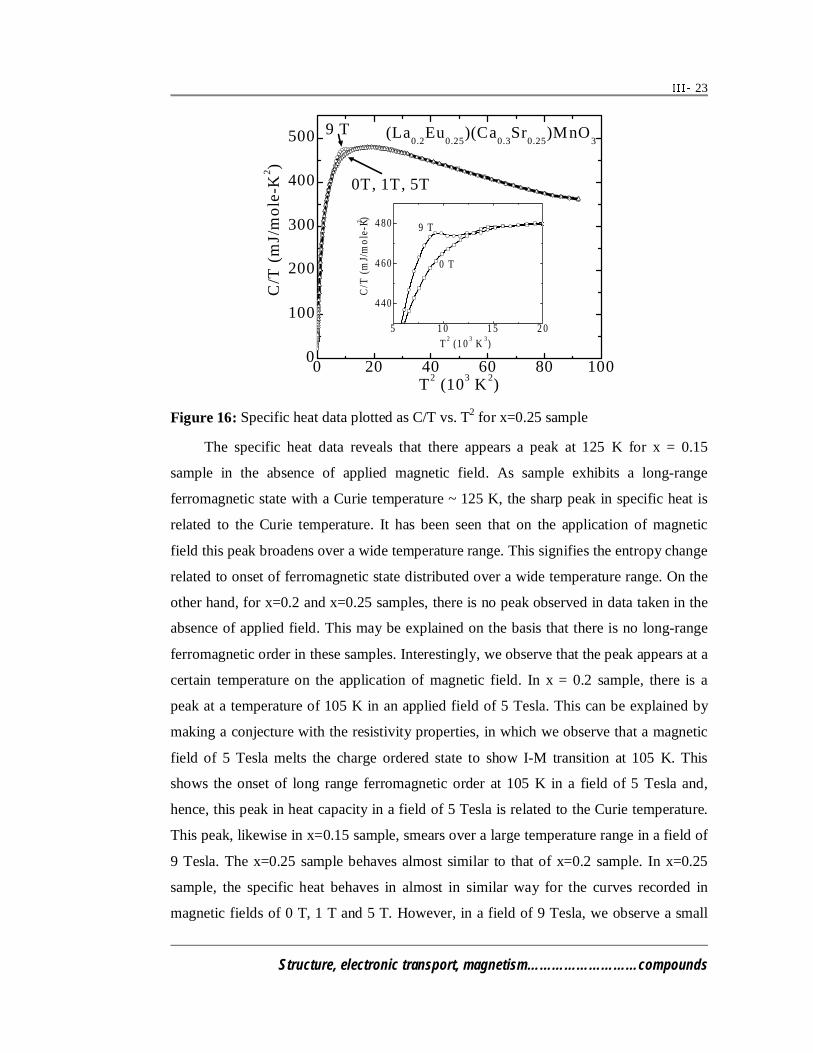
23
Structure, electronic transport, magnetism………………………compounds
0 20 40 60 80 1000
100
200
300
400
500 (La0.2
Eu0.25
)(Ca0.3
Sr0.25
)MnO3
5 1 0 1 5 2 0
4 40
4 60
4 80 9 T
0 T
C/T
(m
J/m
ole-
K2 )
T2 (1 0
3 K
3)
0T, 1T, 5T
9 T
C/T
(m
J/m
ole
-K2 )
T2 (103 K 2)
Figure 16: Specific heat data plotted as C/T vs. T2 for x=0.25 sample
The specific heat data reveals that there appears a peak at 125 K for x = 0.15
sample in the absence of applied magnetic field. As sample exhibits a long-range
ferromagnetic state with a Curie temperature ~ 125 K, the sharp peak in specific heat is
related to the Curie temperature. It has been seen that on the application of magnetic
field this peak broadens over a wide temperature range. This signifies the entropy change
related to onset of ferromagnetic state distributed over a wide temperature range. On the
other hand, for x=0.2 and x=0.25 samples, there is no peak observed in data taken in the
absence of applied field. This may be explained on the basis that there is no long-range
ferromagnetic order in these samples. Interestingly, we observe that the peak appears at a
certain temperature on the application of magnetic field. In x = 0.2 sample, there is a
peak at a temperature of 105 K in an applied field of 5 Tesla. This can be explained by
making a conjecture with the resistivity properties, in which we observe that a magnetic
field of 5 Tesla melts the charge ordered state to show I-M transition at 105 K. This
shows the onset of long range ferromagnetic order at 105 K in a field of 5 Tesla and,
hence, this peak in heat capacity in a field of 5 Tesla is related to the Curie temperature.
This peak, likewise in x=0.15 sample, smears over a large temperature range in a field of
9 Tesla. The x=0.25 sample behaves almost similar to that of x=0.2 sample. In x=0.25
sample, the specific heat behaves in almost in similar way for the curves recorded in
magnetic fields of 0 T, 1 T and 5 T. However, in a field of 9 Tesla, we observe a small

24
Structure, electronic transport, magnetism………………………compounds
peak in specific heat at a temperature of 90 K. This peak too has its origin in onset of
magnetic field induced ferromagnetism.
3.1.5 Magnetoresistance
Possible role of chemical disorder, phase segregation and cluster-glass behavior
Figure 17 shows the magnetoresistance (MR%) vs. temperature (T) plots for
(La0.7-2xEux)(Ca0.3Srx)MnO3 (0.05≤x≤ 0.20) samples in the temperature range of 2K–
320K in various fields up to 5 Tesla.
0 1 0 0 2 0 0 3 0 00
2 0
4 0
6 0
8 0
1 0 0
x = 0 .0 55 T
4 T
3 T
1 T2 T
MR
%
T ( K )
0
2 0
4 0
6 0
8 0
1 0 0
x = 0 .1 05 T
4 T3 T
2 T
1 T
0
2 0
4 0
6 0
8 0
1 0 0( L a
0 . 7 - 2 xE u
x) ( C a
0 . 3S r
x) M n O
3
x = 0 .1 5
1 T
2 T
3 T
4 T
5 T
Figure 17: MR% vs. temperature plots for (La0.7-2xEux)(Ca0.3Srx)MnO3 (0.05≤x≤0.15)
samples.
The MR% of the samples with x=0.05 to 0.15 increases rapidly up to a field of 3
Tesla and then nearly saturates at higher fields. As it has been observed earlier, the CMR

25
Structure, electronic transport, magnetism………………………compounds
effect seems to follow an inverse correlation with Tp [2], with x=0.15 composition
showing a CMR effect of > 90% at a field of 2 Tesla. The CMR effect increases with
increasing x in low temperature ferromagnetic region and is comparable to the effect at
the peak resistivity. To separate the granular contribution and the intrinsic contribution to
MR, we have measured resistivity as a function of magnetic field at constant
temperatures.
0 2 0 4 0 6 0 8 0 1 0 00
2 0
4 0
6 0
8 0
x = 0 . 0 55 K , 5 0 K
2 5 0 K
1 2 0 K1 7 5 K
MR
%M
R%
MR
%
H ( k O e )
0
2 0
4 0
6 0
8 0
x = 0 . 1
2 5 0 K
5 K , 5 0 K
1 2 0 K 1 4 0 K
0
2 0
4 0
6 0
8 0
1 0 0
x = 0 . 1 5
5 K5 0 K
1 3 0 K
2 0 0 K
8 0 K
Figure 18: MR% vs. field (H) plots for (La0.7-2xEux)(Ca0.3Srx)MnO3(0.05≤x≤0.15)
samples.
Figure 18 shows the magnetoresistance as a function of applied field at different
temperatures for all (La0.7-2xEux)(Ca0.3Srx)MnO3 (0.05≤x0.15) samples. As expected, the
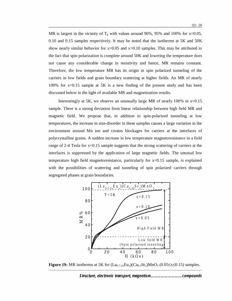
26
Structure, electronic transport, magnetism………………………compounds
MR is largest in the vicinity of Tp with values around 90%, 95% and 100% for x=0.05,
0.10 and 0.15 samples respectively. It may be noted that the isotherms at 5K and 50K
show nearly similar behavior for x=0.05 and x=0.10 samples. This may be attributed to
the fact that spin polarization is complete around 50K and lowering the temperature does
not cause any considerable change in resistivity and hence, MR remains constant.
Therefore, the low temperature MR has its origin in spin polarized tunneling of the
carriers in low fields and grain boundary scattering at higher fields. An MR of nearly
100% for x=0.15 sample at 5K is a new finding of the present study and has been
discussed below in the light of available MR and magnetization results.
Interestingly at 5K, we observe an unusually large MR of nearly 100% in x=0.15
sample. There is a strong deviation from linear relationship between high field MR and
magnetic field. We propose that, in addition to spin-polarized tunneling at low
temperatures, the increase in size-disorder in these samples causes a large variation in the
environment around Mn ion and creates blockages for carriers at the interfaces of
polycrystalline grains. A sudden increase in low temperature magnetoresistance in a field
range of 2-4 Tesla for x=0.15 sample suggests that the strong scattering of carriers at the
interfaces is suppressed by the application of large magnetic fields. The unusual low
temperature high field magnetoresistance, particularly for x=0.15 sample, is explained
with the possibilities of scattering and tunneling of spin polarized carriers through
segregated phases at grain boundaries.
0 2 0 4 0 6 0 8 0 1 0 00
2 0
4 0
6 0
8 0
1 0 0( L a
0.7-2xE u
x) ( C a
0.30S r
x) M n O
3
H ig h F i e l d M R
T = 5 K
L o w f i e ld M R( S p i n p o l a r i s e d tu n n e l in g )
x = 0 . 1 5
x = 0 . 1 0
x = 0 . 0 5
MR
%
H ( k O e )
Figure 19: MR isotherms at 5K for (La0.7-2xEux)(Ca0.3Srx)MnO3 (0.05≤x≤0.15) samples.
27
Structure, electronic transport, magnetism………………………compounds
We have plotted the MR isotherms for all the (La0.7-2xEux)(Ca0.3Srx)MnO3
(0.05≤x0.15) samples at 5K separately in fig. 19 and MR behavior has been divided into
two parts. The MR of nearly 20% below a field of around 5 kOe is the low field MR and
the MR from 20% to 100% in a field of 5 kOe to 90 kOe is the high field MR. At low
fields linear part of the isotherm is low field MR while rest of the contribution in MR
isotherm is due to high field [42-44]. The high field MR varies almost linearly with
applied field [43]. At 5K, the MR in x=0.05 and x=0.10 samples nearly obeys this
behavior. Separating out the contribution of low field MR and high field MR in these
samples, it is clear that high field MR is quite larger than low field MR. In x=0.15
sample The high field MR is almost five times larger than the low field MR. Also, the
high field MR in this sample shows a large deviation from the reported linear
relationship of MR with applied field [43]. The MR increases sharply between 20 kOe to
50 kOe and attains nearly a saturated value of 98%. This MR ~98% at a temperature of
5K for x=0.15 sample is unusually high and interesting.
The MFC-MZFC/MZFC vs. T/TC plot (fig. 6) emphasizes the separation of MZFC and
MFC curves. With decreasing temperature, this separation increases rapidly for x=0.15
sample and points towards the cluster-spin glass behavior of this sample. This has been
verified by performing the frequency dependence of the a.c. susceptibility measurements.
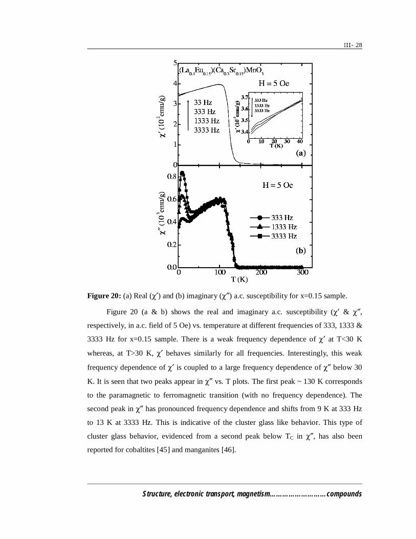
28
Structure, electronic transport, magnetism………………………compounds
Figure 20: (a) Real (χ′) and (b) imaginary (χ″) a.c. susceptibility for x=0.15 sample.
Figure 20 (a & b) shows the real and imaginary a.c. susceptibility (χ′ & χ″,
respectively, in a.c. field of 5 Oe) vs. temperature at different frequencies of 333, 1333 &
3333 Hz for x=0.15 sample. There is a weak frequency dependence of χ′ at T<30 K
whereas, at T>30 K, χ′ behaves similarly for all frequencies. Interestingly, this weak
frequency dependence of χ′ is coupled to a large frequency dependence of χ″ below 30
K. It is seen that two peaks appear in χ″ vs. T plots. The first peak ~ 130 K corresponds
to the paramagnetic to ferromagnetic transition (with no frequency dependence). The
second peak in χ″ has pronounced frequency dependence and shifts from 9 K at 333 Hz
to 13 K at 3333 Hz. This is indicative of the cluster glass like behavior. This type of
cluster glass behavior, evidenced from a second peak below TC in χ″, has also been
reported for cobaltites [45] and manganites [46].

29
Structure, electronic transport, magnetism………………………compounds
The magnetization (M) for x=0.15 sample has been measured as a function of
magnetic field (H) at 5K in which a saturation in magnetization (>3µB) is obtained in a
field of 5 Tesla. The experimental saturation magnetization value is close to that
calculated from the spin only value (3.55µB) of Mn ions, which implies that there is no
spin disorder at Mn ions. Therefore, the origin of the large MR cannot be attributed to
the intrinsic factor of Zener-Double Exchange. However, it is seen from fig. 7 that, for
the x=0.15 sample, there is large deviation in paramagnetic susceptibility from the Curie-
Weiss behavior. This points towards the segregation of both ferromagnetic-metallic and
paramagnetic-insulating phases from the major matrix and the chemical disorder as result
of large size disorder in these samples. We have performed the SEM and detailed EDAX
analysis on these samples, which reveal a compositional disparity in the bulk and on
surface of the grains. This supports our assumption of phase segregation and chemical
disorder, which also results in a large disparity between TC (~130K) and Tp (~78K) for
x=0.15 sample. Phase segregation and disparity between Tp and TC has also been
reported to exist in similar compounds having large size disorder [30]. The possibly
segregated small microscopic insulating phases may occupy positions at the grain
boundaries and increase the resistivity by pinning the Mn ions at the grain surface. This
phase segregation may have a strong correlation with the high field MR.
It has been reported that connectivity between grains and pinning of Mn ions at
grain boundaries play an important role in the conduction of carriers. The high field MR
is due to the opening up of new conduction channels on grain boundaries [47-49]. These
conducting channels open linearly with applied field and, therefore, at higher fields the
MR varies almost linearly with field. In the present case, the unusually large MR
observed in x=0.15 sample at 5K in higher fields may be explained by the possible
existence of microscopic phases embedded between connecting grains. The existence of
such phases and other microscopic phases on the grain interfaces increases the resistivity.
This creates an anisotropic environment of insulating and conducting paths around Mn
ions and blocks the path for carriers at the interfaces. Therefore, the large size disorder
and phase segregation in the present samples largely increases the weight of the
insulating channels. However, in large applied magnetic field, such insulating phases
may start exhibiting metallic behavior and carriers may percolate through such
microscopic phases, thus opening new conduction paths. But, the opening up of new

30
Structure, electronic transport, magnetism………………………compounds
conduction paths is not linear with the applied field. Also, we have evidenced a weak
cluster glass behavior in the temperature range where a large anomalous MR% occurs.
This cluster glass behavior may be a result of large chemical disorder or phase-
segregation in x=0.15 sample. The frozen cluster magnetic moments may align with
large applied magnetic fields leading to large high field MR% at low temperatures. Such
an exceptionally large MR behavior is unusual in the sense that it does not increase
linearly with field in higher fields.
3.1.6 Summary and conclusions
The effects of simultaneous increase in size variance and carrier density on the
electronic and magnetic properties of (La0.7-2xEux)(Ca0.3Srx)MnO3 (0.05≤x≤0.25) system
have been studied. It is found that the lattice distortion and increasing Coulombic
interactions due to increasing size disorder and increasing Mn4+ content are the two
factors, which cause carrier localization. The size disorder increases the spin and
potential fluctuations, favoring the Mott’s type variable range of hopping (VRH) in the
semiconducting region. There is a large contribution of random spin fluctuations to the
resistivity which is evident from the fact that low temperature resistivity obeys higher n
values in the electron-magnon scattering laws. The coexisting FM and AFM charge-
ordered phases in half-doped composition cause phase separation and results in
interesting sharp step like metamagnetic transition which have been observed first time
in any non Pr-based system. At low temperatures, an unusually large high field MR
~100% is observed in x=0.15 sample. Size-disorder induced features such as low
temperature cluster-glass behavior, chemical disorder, possible phase segregation and
contamination of grain surfaces are the factors responsible for such a low temperature
MR%. Application of high field results in the opening of conduction paths in a non-
linear way for blocked Mn spins at the polycrystalline grain boundaries and the
alignment of frozen cluster magnetic moments. This study opens up a new way to
enhance the low temperature magnetoresistance by means of inducing large size-disorder
in heavily hole-doped manganites.
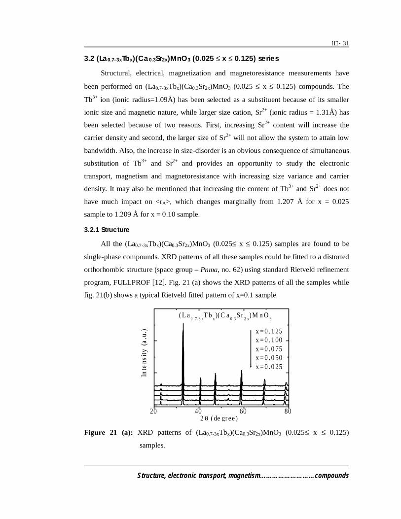
31
Structure, electronic transport, magnetism………………………compounds
3.2 (La0.7-3xTbx)(Ca0.3Sr2x)MnO3 (0.025 ≤ x ≤ 0.125) series
Structural, electrical, magnetization and magnetoresistance measurements have
been performed on (La0.7-3xTbx)(Ca0.3Sr2x)MnO3 (0.025 ≤ x ≤ 0.125) compounds. The
Tb3+ ion (ionic radius=1.09Å) has been selected as a substituent because of its smaller
ionic size and magnetic nature, while larger size cation, Sr2+ (ionic radius = 1.31Å) has
been selected because of two reasons. First, increasing Sr2+ content will increase the
carrier density and second, the larger size of Sr2+ will not allow the system to attain low
bandwidth. Also, the increase in size-disorder is an obvious consequence of simultaneous
substitution of Tb3+ and Sr2+ and provides an opportunity to study the electronic
transport, magnetism and magnetoresistance with increasing size variance and carrier
density. It may also be mentioned that increasing the content of Tb3+ and Sr2+ does not
have much impact on <rA>, which changes marginally from 1.207 Å for x = 0.025
sample to 1.209 Å for x = 0.10 sample.
3.2.1 Structure
All the (La0.7-3xTbx)(Ca0.3Sr2x)MnO3 (0.025≤ x ≤ 0.125) samples are found to be
single-phase compounds. XRD patterns of all these samples could be fitted to a distorted
orthorhombic structure (space group – Pnma, no. 62) using standard Rietveld refinement
program, FULLPROF [12]. Fig. 21 (a) shows the XRD patterns of all the samples while
fig. 21(b) shows a typical Rietveld fitted pattern of x=0.1 sample.
20 40 60 80
( L a0 . 7-3 x
T bx)( C a
0. 3S r
2 x) M n O
3
Inte
nsit
y (
a.u
.)
2 θ ( de gr ee )
x =0 .1 25x =0 .1 00x =0 .0 75x =0 .0 50x =0 .0 25
Figure 21 (a): XRD patterns of (La0.7-3xTbx)(Ca0.3Sr2x)MnO3 (0.025≤ x ≤ 0.125)
samples.
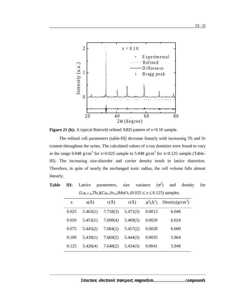
32
Structure, electronic transport, magnetism………………………compounds
2 0 4 0 6 0 8 0
0
1
2 x = 0 .1 0
Inte
nsit
y (a
.u.)
2 θ (d eg ree)
E xpe rim e nta l R ef ine d D iff er en ce B r agg pe a k
Figure 21 (b): A typical Rietveld refined XRD pattern of x=0.10 sample.
The refined cell parameters (table-III) decrease linearly with increasing Tb and Sr
content throughout the series. The calculated values of x-ray densities were found to vary
in the range 6.048 g/cm3 for x=0.025 sample to 5.948 g/cm3 for x=0.125 sample (Table-
III). The increasing size-disorder and carrier density result in lattice distortion.
Therefore, in spite of nearly the unchanged ionic radius, the cell volume falls almost
linearly.
Table III: Lattice parameters, size variance (σ2) and density for
(La0.7-3xTbx)(Ca0.3Sr2x)MnO3 (0.025 ≤ x ≤ 0.125) samples.
x a(Å) c(Å) c(Å) σ2(Å2) Density(g/cm3)
0.025 5.463(1) 7.718(3) 5.471(3) 0.0013 6.048
0.050 5.453(1) 7.698(4) 5.469(3) 0.0020 6.024
0.075 5.445(2) 7.684(1) 5.457(2) 0.0028 6.000
0.100 5.439(1) 7.669(2) 5.444(3) 0.0035 5.964
0.125 5.426(4) 7.648(2) 5.434(3) 0.0041 5.948

33
Structure, electronic transport, magnetism………………………compounds
3.2.2 Electronic transport
Electrical resistivity of (La0.7-3xTbx)(Ca0.3Sr2x)MnO3 (0.025 ≤ x ≤ 0.10) samples
was measured in the temperature range of 320 K – 5 K. Resistivity (ρ) versus
temperature (T) plots [in the form of (ln ρ) vs. T] for these samples are shown in fig. 22.
0 1 00 2 00 3 000
4
8
1 2
1 6
2 0
x= 0 .10
x =0 .0 75
x= 0 .05
x =0 .0 25
( L a0. 7-3 x
T bx) (C a
0. 3S r
2 x)M n O
3
lnρ
( Ω-c
m)
T ( K )
Figure 22: Electrical resistivity vs. temperature plotted as ln ρ vs. T for
(La0.7-3xTbx)(Ca0.3Sr2x)MnO3 (0.025≤ x ≤0.10) samples
All the samples exhibit insulator-metal transition and, except x=0.1 sample
(Tp=118K), show a decreasing trend in Tp from 193K for x = 0.025 to 100K for x =
0.075 sample. The fall in Tp may be attributed to increasing coulombic interactions due
to increasing carrier density and lattice distortion due to increasing size variance. These
factors cause distortion and rotation of MnO6 octahedra and hence disturb the transfer of
conduction electron through Mn-O-Mn network. The x = 0.1 sample does not follow this
trend and is discussed below.
For charge-ordering to occur, regular alternate arrangement of Mn3+ and Mn4+ ions
and critical limit of <rA> should be maintained. The charge-ordering is very sensitive to
size-disorder and <rA> and the large size-disorder melts the charge-ordered state by
causing the random arrangement of Mn3+ and Mn4+ ions [10,11]. The sample with
x = 0.1 is a half-doped composition but does not exhibit charge-ordering. It has larger
size-disorder and <rA> than the standard La0.5Ca0.5MnO3 charge-ordered sample. Hence,
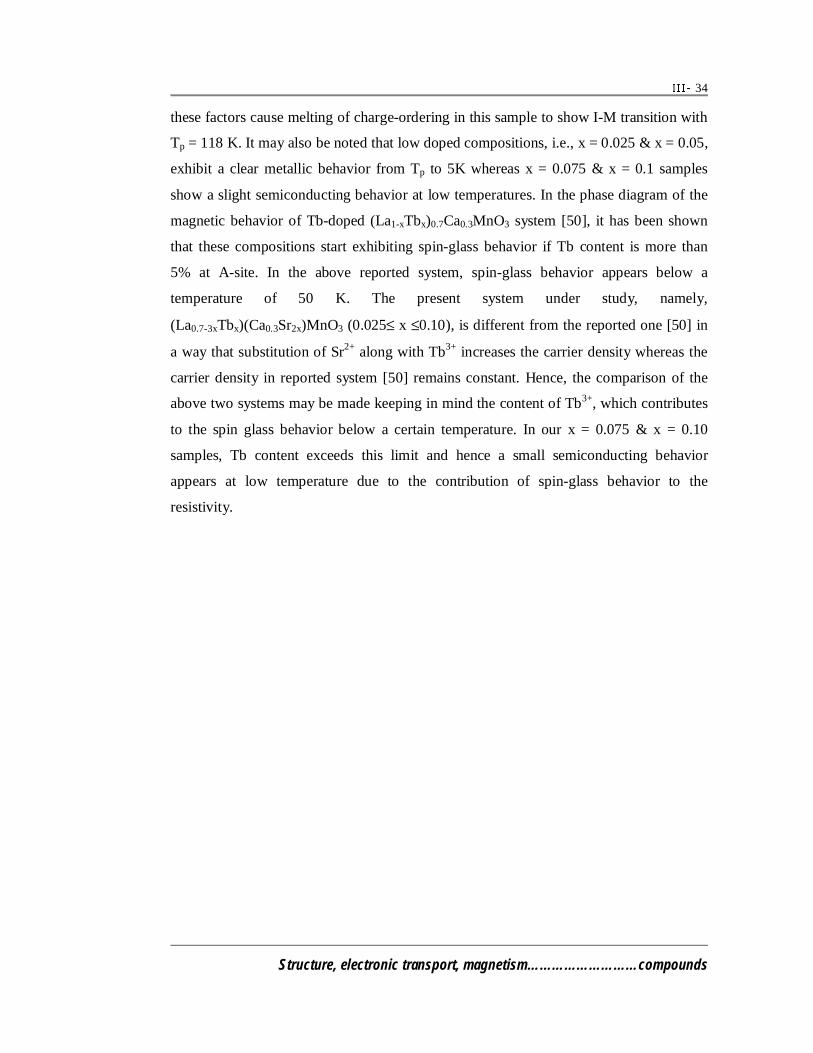
34
Structure, electronic transport, magnetism………………………compounds
these factors cause melting of charge-ordering in this sample to show I-M transition with
Tp = 118 K. It may also be noted that low doped compositions, i.e., x = 0.025 & x = 0.05,
exhibit a clear metallic behavior from Tp to 5K whereas x = 0.075 & x = 0.1 samples
show a slight semiconducting behavior at low temperatures. In the phase diagram of the
magnetic behavior of Tb-doped (La1-xTbx)0.7Ca0.3MnO3 system [50], it has been shown
that these compositions start exhibiting spin-glass behavior if Tb content is more than
5% at A-site. In the above reported system, spin-glass behavior appears below a
temperature of 50 K. The present system under study, namely,
(La0.7-3xTbx)(Ca0.3Sr2x)MnO3 (0.025≤ x ≤0.10), is different from the reported one [50] in
a way that substitution of Sr2+ along with Tb3+ increases the carrier density whereas the
carrier density in reported system [50] remains constant. Hence, the comparison of the
above two systems may be made keeping in mind the content of Tb3+, which contributes
to the spin glass behavior below a certain temperature. In our x = 0.075 & x = 0.10
samples, Tb content exceeds this limit and hence a small semiconducting behavior
appears at low temperature due to the contribution of spin-glass behavior to the
resistivity.
35
Structure, electronic transport, magnetism………………………compounds
0.0 5.0x10⁹ 1.0x10¹⁰ 1.5x10¹⁰ 2.0x10100
200
400
600
(La0.7-3x
Tbx)(Ca
0.3Sr
2x)MnO
3
x=0.025
ρ ( Ω
-cm
)ρ
( Ω-c
m)
ρ ( Ω
-cm
)
T4.5(K4.5)
0.0 2.0x10⁶ 4.0x10⁶ 6.0x10⁶ 8.0x1060
200
400
600
H=5 T
H=0 T
ρ ( Ω
-cm
)
T3(K3)
0 1x10⁹ 2x10⁹ 3x1090
10
20
30
40
H=0 T
H=5 Tx=0.05
ρ (k
Ω-c
m)
ρ (k
Ω-c
m)
ρ (k
Ω-c
m)
T4.5(K4.5)
0 1x10⁶ 2x1060
10
20
30
40
H=0 T
x=0.05
T3(K3)
ρ (k
Ω-c
m)
0
40
80
120
160H=5 T
H=0 T
0
40
80
120
160x=0.025
0
2
4
6
0
2
4
6H=5 T
Figure 23: Fits of resistivity (ρ) to the two-magnon scattering law (ρ versus T4.5), and
unconventional one magnon scattering law (ρ versus T3), in 0 Tesla and in 5
Tesla magnetic field for (La0.7-3xTbx)(Ca0.3Sr2x)MnO3 (x = 0.025 & 0.05)
samples.
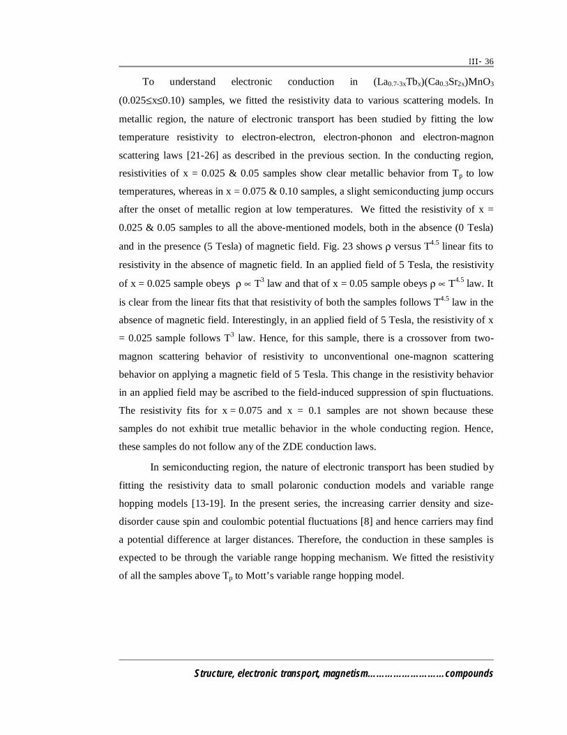
36
Structure, electronic transport, magnetism………………………compounds
To understand electronic conduction in (La0.7-3xTbx)(Ca0.3Sr2x)MnO3
(0.025≤x≤0.10) samples, we fitted the resistivity data to various scattering models. In
metallic region, the nature of electronic transport has been studied by fitting the low
temperature resistivity to electron-electron, electron-phonon and electron-magnon
scattering laws [21-26] as described in the previous section. In the conducting region,
resistivities of x = 0.025 & 0.05 samples show clear metallic behavior from Tp to low
temperatures, whereas in x = 0.075 & 0.10 samples, a slight semiconducting jump occurs
after the onset of metallic region at low temperatures. We fitted the resistivity of x =
0.025 & 0.05 samples to all the above-mentioned models, both in the absence (0 Tesla)
and in the presence (5 Tesla) of magnetic field. Fig. 23 shows ρ versus T4.5 linear fits to
resistivity in the absence of magnetic field. In an applied field of 5 Tesla, the resistivity
of x = 0.025 sample obeys ρ ∝ T3 law and that of x = 0.05 sample obeys ρ ∝ T4.5 law. It
is clear from the linear fits that that resistivity of both the samples follows T4.5 law in the
absence of magnetic field. Interestingly, in an applied field of 5 Tesla, the resistivity of x
= 0.025 sample follows T3 law. Hence, for this sample, there is a crossover from two-
magnon scattering behavior of resistivity to unconventional one-magnon scattering
behavior on applying a magnetic field of 5 Tesla. This change in the resistivity behavior
in an applied field may be ascribed to the field-induced suppression of spin fluctuations.
The resistivity fits for x = 0.075 and x = 0.1 samples are not shown because these
samples do not exhibit true metallic behavior in the whole conducting region. Hence,
these samples do not follow any of the ZDE conduction laws.
In semiconducting region, the nature of electronic transport has been studied by
fitting the resistivity data to small polaronic conduction models and variable range
hopping models [13-19]. In the present series, the increasing carrier density and size-
disorder cause spin and coulombic potential fluctuations [8] and hence carriers may find
a potential difference at larger distances. Therefore, the conduction in these samples is
expected to be through the variable range hopping mechanism. We fitted the resistivity
of all the samples above Tp to Mott’s variable range hopping model.

37
Structure, electronic transport, magnetism………………………compounds
0 .2 4 0 .2 6 0 .2 8 0 .3 0
4
8
1 2
1 6(L a
0.7-3xT b
x)(C a
0.3S r
2x)M n O
3
x= 0 .0 2 5
x= 0 .0 7 5
x= 0 .0 5
x= 0 .1 0
ln ρ
( Ω-c
m)
T -0.25(K -0.25)
Figure 24: lnρ versus T-0.25 for (La0.7-3xTbx)(Ca0.3Sr2x)MnO3 (0.025 ≤ x ≤ 0.10) samples.
In fig. 24, the linear fits of lnρ versus T-0.25 confirm that conduction in these
samples occurs by Mott’s variable range hopping mechanism. We have calculated the
carrier localization length by a modified relation kTo = 171να3Um, given by Viret et al.
[20]. The values of carrier localization length are found to vary in the range 4Å to 5Å for
all the samples [table–IV]. These plausible values confirm that resistivity in the
semiconducting region is a result of magnetic localization.
3.2.3 Magnetic properties
We have carried out magnetization (M) measurements on
(La0.7-3xTbx)(Ca0.3Sr2x)MnO3 (0.025 ≤ x ≤ 0.125) samples in the temperature range of 5 K
– 330 K and in an applied field of 50 Oe, both in Zero-field-cooled (ZFC) and field-
cooled (FC) states. Fig. 25 shows the MFC and MZFC plots for all the samples. It is clear
from the figure that x = 0.025 and x = 0.05 samples have nearly the same Curie
temperature (TC) of about 200 K. The TC falls to 130 K for x = 0.10 sample. It may be
noted that, in the ferromagnetic region, the separation between MFC and MZFC curves
increases with increasing Tb and Sr content.
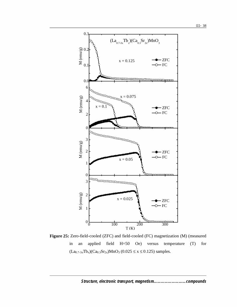
38
Structure, electronic transport, magnetism………………………compounds
0 100 200 3000
1
2
3
x = 0.025
M (
emu/
g)
M (
emu/
g)
T (K)
ZFC FC
0
1
2
3
x = 0.05
ZFC FC
0
2
4
6
x = 0.1
x = 0.075
ZFC FC
M
(em
u/g)
0.0
0.1
0.2
0.3
(La0.7-3x
Tbx)(Ca
0.3Sr
2x)MnO
3
x = 0.125 ZFC FC
M
(em
u/g)
Figure 25: Zero-field-cooled (ZFC) and field-cooled (FC) magnetization (M) (measured
in an applied field H=50 Oe) versus temperature (T) for
(La0.7-3xTbx)(Ca0.3Sr2x)MnO3 (0.025 ≤ x ≤ 0.125) samples.
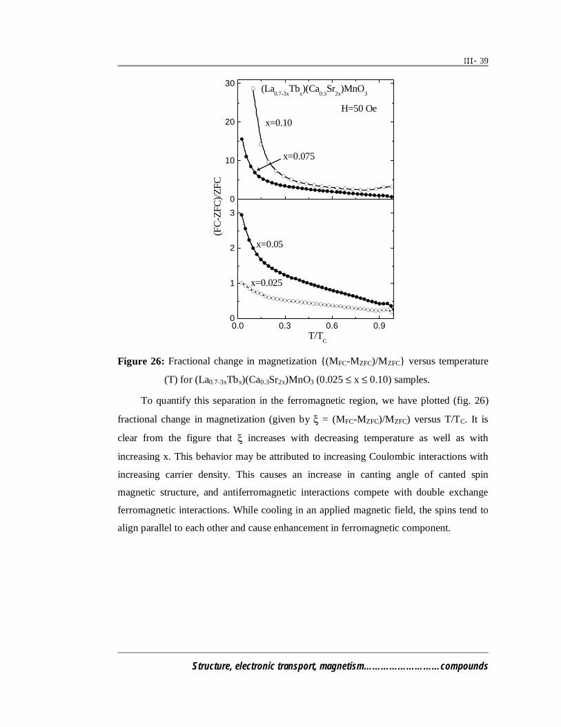
39
Structure, electronic transport, magnetism………………………compounds
0.0 0.3 0.6 0.90
1
2
3
x=0.05
(FC
-ZFC
)/Z
FC
T/TC
0
10
20
30
H=50 Oe
x=0.075
x=0.10
x=0.025
(La0.7-3x
Tbx)(Ca
0.3Sr
2x)MnO
3
Figure 26: Fractional change in magnetization (MFC-MZFC)/MZFC versus temperature
(T) for (La0.7-3xTbx)(Ca0.3Sr2x)MnO3 (0.025 ≤ x ≤ 0.10) samples.
To quantify this separation in the ferromagnetic region, we have plotted (fig. 26)
fractional change in magnetization (given by ξ = (MFC-MZFC)/MZFC) versus T/TC. It is
clear from the figure that ξ increases with decreasing temperature as well as with
increasing x. This behavior may be attributed to increasing Coulombic interactions with
increasing carrier density. This causes an increase in canting angle of canted spin
magnetic structure, and antiferromagnetic interactions compete with double exchange
ferromagnetic interactions. While cooling in an applied magnetic field, the spins tend to
align parallel to each other and cause enhancement in ferromagnetic component.
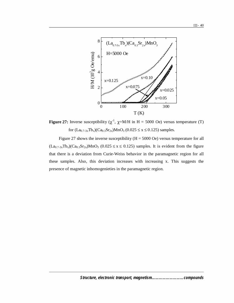
40
Structure, electronic transport, magnetism………………………compounds
0 100 200 3000
2
4
6
8
x=0.05
x=0.10
x=0.075x=0.025
(La0.7-3x
Tbx)(Ca
0.3Sr
2x)MnO
3
H=5000 Oe
x=0.125
H/M
(10
3 g O
e/em
u)
T (K)
Figure 27: Inverse susceptibility (χ-1, χ=M/H in H = 5000 Oe) versus temperature (T)
for (La0.7-3xTbx)(Ca0.3Sr2x)MnO3 (0.025 ≤ x ≤ 0.125) samples.
Figure 27 shows the inverse susceptibility (H = 5000 Oe) versus temperature for all
(La0.7-3xTbx)(Ca0.3Sr2x)MnO3 (0.025 ≤ x ≤ 0.125) samples. It is evident from the figure
that there is a deviation from Curie-Weiss behavior in the paramagnetic region for all
these samples. Also, this deviation increases with increasing x. This suggests the
presence of magnetic inhomogenieties in the paramagnetic region.
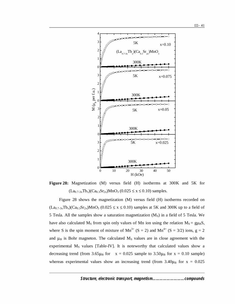
41
Structure, electronic transport, magnetism………………………compounds
0 10 20 30 40 500
1
2
3
300K
5K
(La0.7-3x
Tbx)(Ca
0.3Sr
2x)MnO
3
x=0.025
M (
µ B p
er f
.u.)
H (kOe)
0
1
2
3
300K
5K x=0.05
0
1
2
3
300K
5K x=0.075
0
1
2
3
4
300K
5K x=0.10
Figure 28: Magnetization (M) versus field (H) isotherms at 300K and 5K for
(La0.7-3xTbx)(Ca0.3Sr2x)MnO3 (0.025 ≤ x ≤ 0.10) samples.
Figure 28 shows the magnetization (M) versus field (H) isotherms recorded on
(La0.7-3xTbx)(Ca0.3Sr2x)MnO3 (0.025 ≤ x ≤ 0.10) samples at 5K and 300K up to a field of
5 Tesla. All the samples show a saturation magnetization (MS) in a field of 5 Tesla. We
have also calculated MS from spin only values of Mn ion using the relation MS = gµBS,
where S is the spin moment of mixture of Mn3+ (S = 2) and Mn4+ (S = 3/2) ions, g = 2
and µB is Bohr magneton. The calculated MS values are in close agreement with the
experimental MS values [Table-IV]. It is noteworthy that calculated values show a
decreasing trend (from 3.65µB for x = 0.025 sample to 3.50µB for x = 0.10 sample)
whereas experimental values show an increasing trend (from 3.40µB for x = 0.025

42
Structure, electronic transport, magnetism………………………compounds
sample to 3.65µB for x = 0.10 sample). This is attributed to the addition of magnetic
moments of Tb3+ to the spin moment of Mn ion. Also, the field, where saturation is
achieved, increases as the Tb and Sr content increases.
Table-IV: I-M transition temperature (Tp), Curie Temperature (TC), carrier localization
length (L) and saturation magnetization (MS) values (observed and
calculated) for (La0.7-3xTbx)(Ca0.3Sr2x)MnO3 (0.025≤x≤0.10) samples.
x Tp (K) TC (K) L (Å) MS (µB)
(Observed)
MS (µB)
(Calculated)
0.025 192 200 5.0 3.40 3.65
0.050 138 205 4.4 3.54 3.60
0.075 100 182 4.3 3.61 3.55
0.100 118 125 4.9 3.65 3.50
Like previous series, this (La0.7-3xTbx)(Ca0.3Sr2x)MnO3 (0.025 ≤ x ≤ 0.125) series of
samples also display a disparity between TC and Tp. The disparity can be understood on
the basis of phase segregation, which is also evident from magnetic measurements. The
deviation from the Curie-Weiss behavior points towards the presence of segregated
ferromagnetic phases in paramagnetic region of the major matrix. Similarly, the
paramagnetic-insulating phases may exist in the ferromagnetic region. Also, the increase
in size variance, with increasing dopant concentration, disturbs the arrangement of Mn3+
and Mn4+ ions. This causes the existence of small paramagnetic-insulating phases of
La/Tb-Ca/Sr-Mn-O in the major ferromagnetic metallic matrix. Also, the regions
adjacent to insulating La/Tb-Ca/Sr-Mn-O phases get distorted and influence
conductivity. When the Curie temperature of ferromagnetic-metallic matrix sets in, the
resistivity of segregated paramagnetic-insulating phases keeps rising and does not allow
the major ferromagnetic matrix to exhibit metallic behavior. It is only after the resistivity
of insulating phases saturates that the metallic phases start percolating and the sample
starts showing the metallic behavior.

43
Structure, electronic transport, magnetism………………………compounds
3.2.4 Magnetoresistance
Magnetoresistance measurements on (La0.7-3xTbx)(Ca0.3Sr2x)MnO3 (0.025≤x≤0.125)
samples were made in a field of 9 Tesla. Fig. 29 shows the variation of
magnetoresistance with magnetic field at different temperatures for all the samples.
0
2 0
4 0
6 0
8 0
10 0
x = 0 .02 5
T= 5 K T= 1 0 0 K T= 1 3 5 K T= 1 7 5 K T= 1 9 0 K T= 2 5 0 K
x = 0.0 5
T= 5 K T = 5 0 K T= 1 0 0 K T= 1 3 5 K T= 1 7 5 K T= 2 5 0 K
0 2 0 4 0 6 0 8 00
2 0
4 0
6 0
8 0
10 0
MR
%
H (kO e )
x = 0 .07 5 T= 5 K T = 5 0 K T = 8 0 K T= 1 0 0 K T= 1 3 0 K T= 2 0 0 K
MR
%
H (kO e )0 2 0 4 0 6 0 8 0
x = 0 .1
T= 5 K T = 2 5 K T = 5 0 K T= 1 2 0 K T= 1 4 0 K T= 2 5 0 K
Figure 29: Magnetoresistance (MR%) vs. field (H) isotherms for
(La0.7-3xTbx)(Ca0.3Sr2x)MnO3 (0.025 ≤ x ≤ 0.1) samples.
It may be seen in the fig. that MR% increases as the doping content increases and
reaches a maximum values of ~100% for x = 0.1 sample. Also, a large MR% occurs in
low temperature region, which is comparable to the MR% in the vicinity of the resistivity
peak. The large low temperature magnetoresistance in (La0.7-3xTbx)(Ca0.3Sr2x)MnO3
(0.025 ≤ x ≤ 0.125) may be attributed to grain boundary effects and large size disorder.
In the present case, all the compositions have large size-disorder. This resulting large

44
Structure, electronic transport, magnetism………………………compounds
size disorder at A-site causes a structural distortion and hence more magnetic disorder at
Mn-O-Mn bonds, which finally increases the resistivity. Also, the carriers may be
scattered at the grain interfaces. This scattering of the carriers at the interfaces and
reduction in scattering on the application of magnetic field may be understood in the
following way. When an electron moves from one grain to the other, it may experience
insulating barrier of interfaces of the first and second grain each of which may scatter it.
This cause of scattering centre of the carriers is at the pinned Mn ion spins at the
interfaces is due to poor connectivity between the grains or surface contamination [47-
49]. Therefore, these pinned Mn ions spins at the interfaces block the conduction paths
of carriers. The scattering of carriers due to pinning of Mn ions at the interfaces and due
to distortion at Mn-O-Mn bonds may be strong or weak in nature. The strong scattering
may be suppressed by the application of a large magnetic field. Therefore, we observe
large high field magnetoresistance at low temperatures.
3.2.5 Conclusions
Structural, electrical, magnetic and magnetoresistive properties of
(La0.7-3xTbx)(Ca0.3Sr2x)MnO3 (0.025≤x≤0.125) samples have been studied. As compared
to the classic La1-xCaxMnO3 (x=0.3-0.5) compositions [2], the increasing size disorder
with carrier density in these samples, induces a variety of rich properties such as phase
segregation, melting of charge ordering state in half doped composition, disorder induced
increase in resistivity and large MR at low temperatures. As a result of spin and
Columbic potential fluctuations developed due to increasing carrier density and size-
disorder, the electronic conduction in these samples is dominated by Mott’s variable
range hopping mechanism in semiconducting region. In the metallic region, the increase
in resistivity with increasing x may be attributed to the various electron-electron,
electron-phonon and electron-magnon scattering phenomena. The segregation of small
paramagnetic-insulating phases from the major matrix causes disparity between metal-
insulator transition temperature (Tp) and paramagnetic-ferromagnetic transition
temperature (TC). Also, MR% increases with increasing x and, particularly at low
temperatures, becomes comparable in magnitude to that at Tp. This is due to enhanced
inter-grain tunneling magnetoresistance at low temperatures, arising as a result of
varying Mn environment at the interfaces.

45
Structure, electronic transport, magnetism………………………compounds
REFERENCES
1. R. Von Helmolt, J. Wecker, B. Holzapfel, L. Schultz and K. Samwer, Phys.
Rev. Lett. 71, 2331 (1993).
2. A. P. Ramirez, J. of Phys.: Condens. Matter 9, 8171 (1997) and references
therein.
3. A. J. Millis, P.B. Littlewood and B.I. Shriaman, Phys. Rev. Lett. 74, 5144
(1995).
4. Y. Yamada, O. Hino, S. Nohdo, R. Kanao, T. Inami and S. Katano, Phys. Rev.
Lett. 77, 904 (1996).
5. J.B. Goodenough, Annu. Rev. Sci. 28, 1 (1998).
6. H.Y.Hwang, S.-W. Cheong, P.G. Radaelli, M. Marezio and B. Batlogg, Phys.
Rev. Lett. 75, 914 (1995).
7. L.M. Rodriguez-Martinez and J.P. Attfield, Phys. Rev. B 54, 15622 (1996).
8. L.M. Rodriguez-Martinez and J.P. Attfield, Phys Rev. B 58, 2426 (1998).
9. P.V. Vanitha, P.N. Santhosh, R.S. Singh and C.N.R. Rao, J.P. Attfield, Phys.
Rev. B 59, 13539 (1999).
10. Y.Q. Gong, Ian Maclaren, X.F. Duan, Z.H. Wang and B.G. Shen, J. Appl. Phys.
90, 488 (2001).
11. Y.Q. Gong, Ian Maclaren, X.F. Duan, Z.H. Wang and B.G. Shen, Appl. Phys.
Lett. 78, 2157 (2001).
12. J. Rodriguez_Carvajel, FULLPROF version 3.0 Laboratorie Leon Brillioun,
CEA-CNRS, (1995).
13. G. Synder, R. Hiskes, S. Dicarolis, M. Beasley and T. Geballe, Phys. Rev. B
53, 14434 (1996).
14. D. Emin and T. Holstein, Phys. Rev. B 13, 647 (1976).
15. Michael Ziese and Chatchai Srinitiwarawong, Phys. Rev. B 58, 11519 (1998).
16. A. L. Efros and B.L. Shklovskii, J. Phys. C 8, L49 (1975).
17. J.M.D. Coey, M. Viret, L. Ranno and K. Ounadjela, Phys. Rev. Lett. 75, 3910
(1995).

46
Structure, electronic transport, magnetism………………………compounds
18. M. Viret, L. Ranno and J.M.D. Coey, J. Appl. Phys. 81, 4964 (1997).
19. Young Sun, Xiaojun Xu and Yuheng Zhang, J. Phys.: Condens. Matter 12,
10475 (2000).
20. M. Viret, L. Ranno and J.M.D. Coey, Phys. Rev. B 55, 8067 (1997).
21. A. Urushibara, Y. Moritomo, T. Amira, A. Asamitsu, G. Kido and Y. Tokura,
Phys. Rev. B 51, 14103 (1995).
22. L. Pi, L. Zhang and Y. Zhang, Phys. Rev. B 61, 8917 (2002).
23. Nobuo Furukawa, J. Phys. Soc. Japan 69, 1954 (2000).
24. J. Li, C. K. Ong, Q. Zhan and D. X. Li, J. Phys.: Condens. Matter 14, 6341
(2002).
25. M. B. Salamon and M. Jaime, Rev. Mod. Phys. 73, 583 (2001).
26. Q. Huang, Z.W. Li, J. Li and C.K. Ong, J. Phys.: Condens. Matter 13, 4033
(2001)
27. R. Mahendiran, M. Hervieu, A. Maignan, C. Martin and B. Raveau, Solid State
Commun. 114, 429 (2000).
28. A. K. Hielman, Y.Y. Xue, B. Lorenz, B.J. Campbell, J. Cmaidalka, R.L. Wang
and C.W. Chu, Phys. Rev. B 65, 214423 (2002).
29. Hirotoshi Terashita and J.J. Neumeirer, Phys. Rev. B 63, 174436 (2001).
30. M. Tokunaga, N, Miura, Y. Tomioka, Y. Tokura, Phys. Rev. B 57, 5259(1998).
31. S. Hebert, V. Hardy, A. Maignan, R. Mahendiran, M. Hervieu, C. Martin, B.
Raveau, J. of Solid State Chem. 165, 6 (2002).
32. R. Mahendiran, A. Maignan, S. Hebert, C. Martin, M. Hervieu, B. Raveau, J.F.
Mitchell and P. Schiffer, Phys. Rev. Lett. 89, 286602 (2002).
33. V. Hardy, A. Maignan, S. Hebert and C. Martin, Phys. Rev. B 67, 24401
(2003).
34. V. Hardy, S. Hebert, L. Herve, A. Maignan, C. Martin, C. Yaicle, M. Hervieu,
B. Raveau, J. Magn. Mag. Maters. 264, 183 (2003).

47
Structure, electronic transport, magnetism………………………compounds
35. V. Hardy, S. Majumdar, S.J. Crowe, M.R. Lees, D. McK. Paul, L. Herve, A.
Maignan, S. Hebert, C. Martin, C. Yaicle, M. Hervieu, B. Raveau, Phys. Rev. B
69, 020407 (2004).
36. A. Maignan, S. Hebert, V. Hardy, C. Martin, M. Hervieu, B. Raveau, J. Phys.:
Condens. Matter 14, 11809 (2002).
37. Eduard Vives and Antoni Planes, Phys. Rev. B 50, 3839 (1994); Eduard Vives,
Jordi Ortin, Lluis Manosa, Ramon Perez-Magrane and Antoni Planes, Phys.
Rev. Lett. 72, 1694 (1994).
38. P.J. Cote and L.V. Meisel, Phys. Rev. Lett. 67, 1334(1991); L.V. Meisel and
P.J. Cote, Phys. Rev. B 46, 10822 (1992).
39. M. Roy., J. F. Mitchell, S. J. Potashnik, and P. Schiffer, J. Magn. Mag. Mater.
218, 191 (2000).
40. L. Ghivelder et al. cond-mat 0308141 (unpublished).
41. S. Yunoki, J. Hu, A.L. Malvezzi, A. Moreo, N. Furukawa, E. Dogotto, Phys.
Rev. Lett. 80, 845 (1998).
42. A. Gupta, G. Q. Gong, G. Xiao, P. R. Duncombe, P. Lecoeur, P. Trouilloud, Y.
Y. Wang, V. P. Dravid and J. Z. Sun, Phys. Rev. B 54, 15629 (1996)
43. H. Y. Hwang, S.-W Cheog, N. P. Ong, and B. Batlogg, Phys. Rev. Lett. 77,
2041 (1996)
44. H. L. Ju, Hyunchul Sohn, Solid State Commun. 102, 463 (1997).
45. D.N.H. Nam, K. Jonason, P. Nordblad, N.V. Kheim, N.X. Phuc, Phys. Rev. B
59, 4189 (1999).
46. L. Ghivelder, I.A. Castillo, M.A. Alonso, L.F. Cohen, Phys. Rev. B 60, 12184
(1999)
47. A. de Andres, M. Garcia-Hernandez, J. L. Martinez, C. Preito, Appl. Phys Letts
74, 3884 (1999).
48. A. de Andres, M. Garcia-Hernandez, J. L. Martinez, Phys. Rev. B 60, 7328
(1999).
49. Sheng Ju, H. Sun and Zhen-Ya Li, Phys. Letts A 300, 666 (2002)
50. J. C. Nie, J. H. Wang and B. R. Zhao, J. Mag. Magn. Maters. 192, L379 (1999).

Chapter – 4
Effect of size-disorder on electronic transport and
magnetism of half-doped (LaTb)0.5(CaSr)0.5MnO3 and
largely hole-doped (LaR)0.55(CaSr)0.45MnO3 systems
4.1 Studies on (LaTb)0.5(CaSr)0.5MnO3 system IV-1
4.1.1 Structure IV-2
4.1.2 Magnetic properties IV-3
4.1.3 Electronic transport IV-5
4.1.4 Magnetoresistance IV-7
4.1.5 Conclusions IV-8
4.2 Studies on (LaR)0.55(CaSr)0.45MnO3 system IV-9
4.2.1 Structure IV-10
4.2.2 Electronic transport IV-11
4.2.3 Magnetic properties IV-14
4.2.4 Magnetoresistance IV-17
4.2.5 Conclusions IV-19
References IV-21

1
Effect of size-disorder on ………………………..systems
4.1 Electrical and magnetic properties of half-doped
(LaTb)0.5(CaSr)0.5MnO3 compounds
The half-doped manganite compounds such as La0.5Ca0.5MnO3 and Nd0.5Sr0.5MnO3,
etc. have attracted the attention due to the interesting charge and orbital ordering
correlations exhibited by them [1,2]. These compounds show transformation from a
ferromagnetic (FM)-metallic state to an antiferromagnetic (AFM) charge ordered (CO)
state at a certain temperature below Curie point (TC) [1,2]. The co-existence of AFM and
CO states has its origin in long-range co-operative Jahn-Teller effect and regular
alternate arrangement of Mn3+ and Mn4+ ions i.e. real space ordering of Mn3+ and Mn4+
ions [1]. This CO state is sensitive to external factors such as applied magnetic field and
pressure and internal factors like chemical pressure resulting from varying average A-site
cation radius and mismatch in ionic size of the different cations occupying A-site [1-4].
There are several studies on the effect of average A-site cationic radius (<rA>) and size
mismatch on melting of AFM CO state leading to an FM metallic state [1,3,4]. In this
section, the results of studies on the simultaneous effect of substitution of a magnetic ion,
Tb3+, and a divalent cation, Sr2+ on the electronic, magnetic and magnetotransport
properties of a half-doped La0.5Ca0.5MnO3 system have been presented. The
(La0.5-xTbx)(Ca0.38-ySr0.12+y)MnO3 (0.025≤x≤0.125; y=0.8x) (LTCSMO) system has been
such that <rA> remains constant at ~ 1.215Å but A-site cation size disorder increases
from 0.0021Å2 to 0.0042Å2 (size disorder is given by σ2=Σxiri2-<rA>2). The choice of
Tb3+ has been has been made with two fold interests, namely, size effect and magnetic
nature. The <rA> of this system is intermediate of two widely studied charge-ordered
systems – La0.5Ca0.5MnO3 (<rA>=1.198Å) and Nd0.5Sr0.5MnO3 (<rA>=1.23Å). Electrical
and magnetization measurements on the samples studied reveal that AFM CO state does
not manifest and system exhibits Curie temperature (TC), insulator-metal (I-M) transition
at Tp and a large magnetoresistance effect.
Synthesis
Three polycrystalline samples of (La0.5-xTbx)(Ca0.38-ySr0.12+y)MnO3 (0.025≤x≤0.125;
y=0.8x) were synthesized using solid state reaction method. Dried powders of La2O3,
Tb2O3, CaCO3, SrCO3 and MnO2 were mixed in stoichiometric proportions and calcined
at 950°C for 24 hours. The samples were then ground, palletized and sintered in a
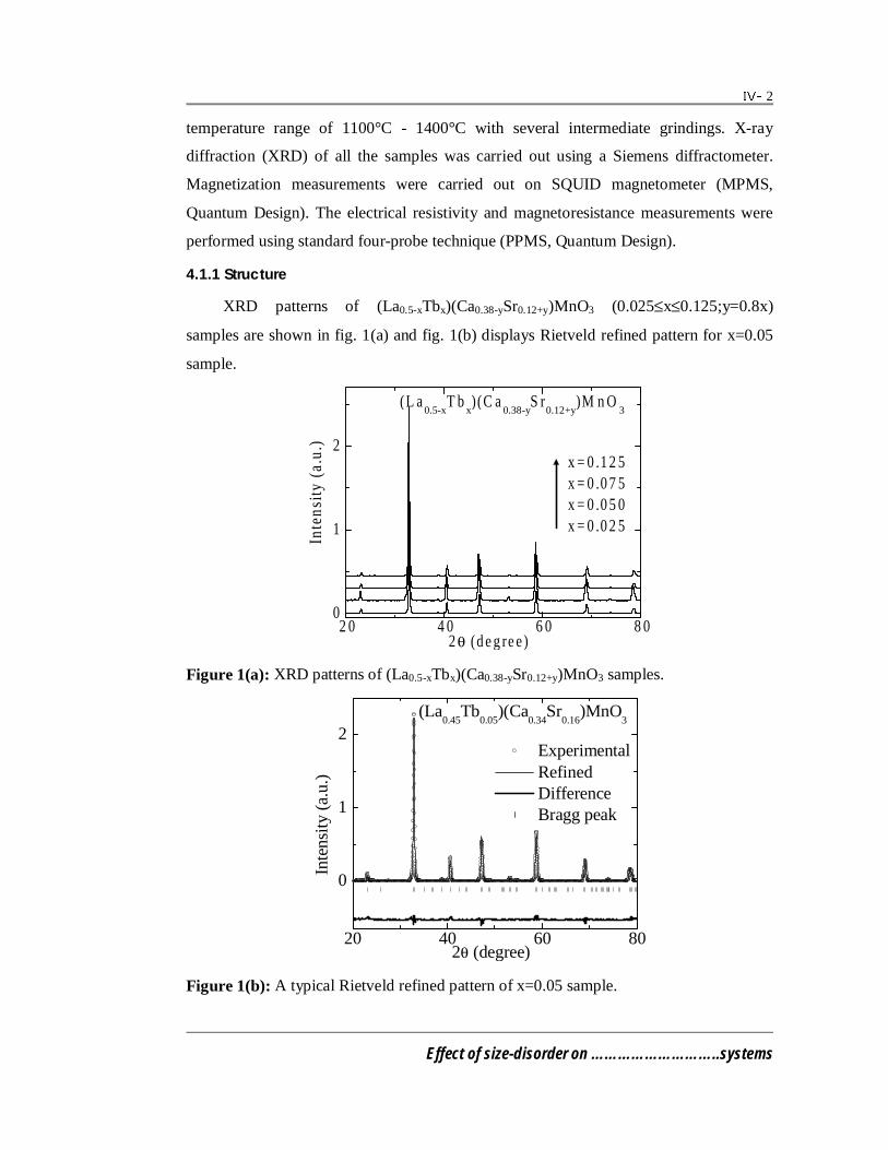
2
Effect of size-disorder on ………………………..systems
temperature range of 1100°C - 1400°C with several intermediate grindings. X-ray
diffraction (XRD) of all the samples was carried out using a Siemens diffractometer.
Magnetization measurements were carried out on SQUID magnetometer (MPMS,
Quantum Design). The electrical resistivity and magnetoresistance measurements were
performed using standard four-probe technique (PPMS, Quantum Design).
4.1.1 Structure
XRD patterns of (La0.5-xTbx)(Ca0.38-ySr0.12+y)MnO3 (0.025≤x≤0.125;y=0.8x)
samples are shown in fig. 1(a) and fig. 1(b) displays Rietveld refined pattern for x=0.05
sample.
2 0 4 0 6 0 8 00
1
2
(L a0.5-x
T bx)(C a
0.38-yS r
0.12+y)M n O
3
x = 0 .1 2 5x = 0 .0 7 5x = 0 .0 5 0x = 0 .0 2 5
Inte
nsit
y (a
.u.)
2 θ (d e g re e )
Figure 1(a): XRD patterns of (La0.5-xTbx)(Ca0.38-ySr0.12+y)MnO3 samples.
20 40 60 80
0
1
2(La
0.45Tb
0.05)(Ca
0.34Sr
0.16)MnO
3
Inte
nsit
y (a
.u.)
2θ (degree)
Experimental Refined Difference Bragg peak
Figure 1(b): A typical Rietveld refined pattern of x=0.05 sample.
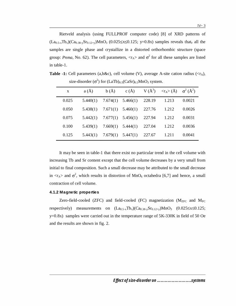
3
Effect of size-disorder on ………………………..systems
Rietveld analysis (using FULLPROF computer code) [8] of XRD patterns of
(La0.5-xTbx)(Ca0.38-ySr0.12+y)MnO3 (0.025≤x≤0.125; y=0.8x) samples reveals that, all the
samples are single phase and crystallize in a distorted orthorhombic structure (space
group: Pnma, No. 62). The cell parameters, <rA> and σ2 for all these samples are listed
in table-1.
Table -1: Cell parameters (a,b&c), cell volume (V), average A-site cation radius (<rA),
size-disorder (σ2) for (LaTb)0.5(CaSr)0.5MnO3 system.
x a (Å) b (Å) c (Å) V (Å3) <rA> (Å) σ2 (Å2)
0.025 5.440(1) 7.674(1) 5.466(1) 228.19 1.213 0.0021
0.050 5.438(1) 7.671(1) 5.460(1) 227.76 1.212 0.0026
0.075 5.442(1) 7.677(1) 5.456(1) 227.94 1.212 0.0031
0.100 5.439(1) 7.669(1) 5.444(1) 227.04 1.212 0.0036
0.125 5.443(1) 7.679(1) 5.447(1) 227.67 1.211 0.0041
It may be seen in table-1 that there exist no particular trend in the cell volume with
increasing Tb and Sr content except that the cell volume decreases by a very small from
initial to final composition. Such a small decrease may be attributed to the small decrease
in <rA> and σ2, which results in distortion of MnO6 octahedra [6,7] and hence, a small
contraction of cell volume.
4.1.2 Magnetic properties
Zero-field-cooled (ZFC) and field-cooled (FC) magnetization (MZFC and MFC
respectively) measurements on (La0.5-xTbx)(Ca0.38-ySr0.12+y)MnO3 (0.025≤x≤0.125;
y=0.8x) samples were carried out in the temperature range of 5K-330K in field of 50 Oe
and the results are shown in fig. 2.
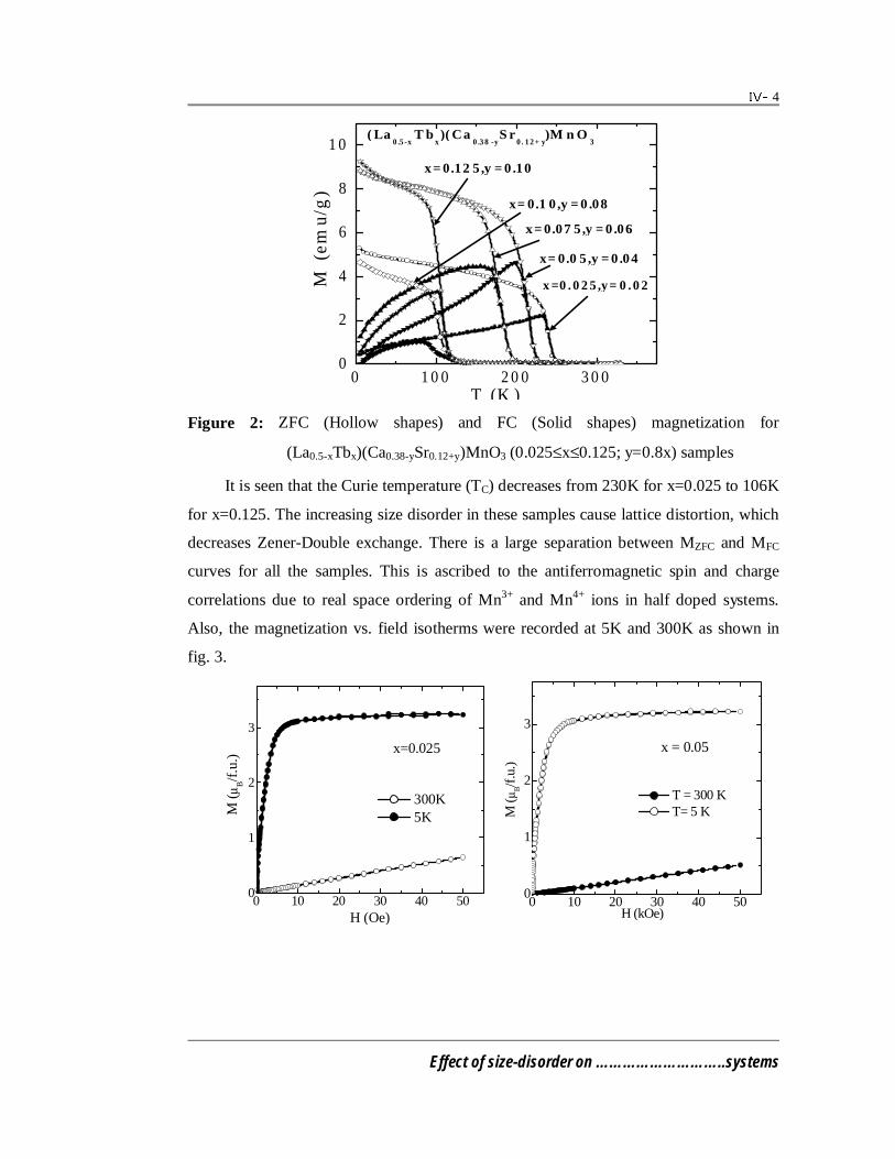
4
Effect of size-disorder on ………………………..systems
0 1 0 0 2 0 0 3 0 00
2
4
6
8
1 0( La
0 .5 -xT b
x)( Ca
0 .3 8 -yS r
0 . 1 2 + y)M n O
3
x= 0.07 5 ,y = 0 .06
x= 0.1 0 ,y = 0 .08
x= 0.12 5 ,y = 0 .10
x= 0.0 5 ,y = 0 .04
x =0 . 0 2 5 ,y= 0 . 0 2
M (
emu/
g)
T (K )
Figure 2: ZFC (Hollow shapes) and FC (Solid shapes) magnetization for
(La0.5-xTbx)(Ca0.38-ySr0.12+y)MnO3 (0.025≤x≤0.125; y=0.8x) samples
It is seen that the Curie temperature (TC) decreases from 230K for x=0.025 to 106K
for x=0.125. The increasing size disorder in these samples cause lattice distortion, which
decreases Zener-Double exchange. There is a large separation between MZFC and MFC
curves for all the samples. This is ascribed to the antiferromagnetic spin and charge
correlations due to real space ordering of Mn3+ and Mn4+ ions in half doped systems.
Also, the magnetization vs. field isotherms were recorded at 5K and 300K as shown in
fig. 3.
0 10 20 30 40 50
0
1
2
3
x=0.025
M (
µ B/f
.u.)
H (Oe)
300K 5K
0 10 20 30 40 50
0
1
2
3
x = 0.05
M (
µ B/f
.u.)
H (kOe)
T = 300 K T= 5 K

5
Effect of size-disorder on ………………………..systems
0 10 20 30 40 50
0
1
2
3
x = 0.10
M (µ
B/f
.u.)
H (kOe)
300 K 5 K
0 10 20 30 40 50
0
1
2
3
x = 0.125
300K
5K
M( µ
B/f
.u.)
H (kOe)
Figure 3: Magnetization isotherms for (La0.5-xTbx)(Ca0.38-ySr0.12+y)MnO3
(x=0.025,0.05,0.1,0.125) samples.
4.1.3 Electronic transport
Figure 4 shows, resistivity versus temperature for (La0.5-xTbx)(Ca0.38-ySr0.12+y)MnO3
(0.025≤x≤0.125; y=0.8x) samples in the temperature range of 5K-320K. It is seen from
the fig. 4 that resistivity increases and Tp decreases with increasing Tb and Sr content. It
may also be noticed that large size disorder in these samples does not allow the
occurrence of AFM CO state and suppresses the Curie point and Tp.
0 1 00 2 00 3 003
6
9
12
15(L a
0. 5 -xT b
x)(C a
0 .3 8 -yS r
0 .1 2 +y)M nO
3
x=0 .1 2 5
x =0 .1 0
x =0 .0 5
x=0 .0 7 5
x=0 .0 2 5
lnρ
( Ω-c
m)
T (K )
Figure 4: Resistivity vs. temperature for (La0.5-xTbx)(Ca0.38-ySr0.12+y)MnO3
(0.025≤x≤0.125; y=0.8x) samples.
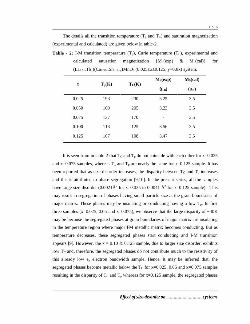
6
Effect of size-disorder on ………………………..systems
The details all the transition temperature (Tp and TC) and saturation magnetization
(experimental and calculated) are given below in table-2.
Table - 2: I-M transition temperature (Tp), Curie temperature (TC), experimental and
calculated saturation magnetization MS(exp) & MS(cal) for
(La0.5-xTbx)(Ca0.38-ySr0.12+y)MnO3 (0.025≤x≤0.125; y=0.8x) system.
x Tp(K) TC(K) MS(exp)
(µB)
MS(cal)
(µB)
0.025 193 230 3.25 3.5
0.050 160 205 3.23 3.5
0.075 137 170 - 3.5
0.100 118 125 3.56 3.5
0.125 107 108 3.47 3.5
It is seen from in table-2 that TC and Tp do not coincide with each other for x=0.025
and x=0.075 samples, whereas TC and Tp are nearly the same for x=0.125 sample. It has
been reported that as size disorder increases, the disparity between TC and Tp increases
and this is attributed to phase segregation [9,10]. In the present series, all the samples
have large size disorder (0.0021Å2 for x=0.025 to 0.0041 Å2 for x=0.125 sample). This
may result in segregation of phases having small particle size at the grain boundaries of
major matrix. These phases may be insulating or conducting having a low Tp. In first
three samples (x=0.025, 0.05 and x=0.075), we observe that the large disparity of ~40K
may be because the segregated phases at grain boundaries of major matrix are insulating
in the temperature region where major FM metallic matrix becomes conducting. But as
temperature decreases, these segregated phases start conducting and I-M transition
appears [9]. However, the x = 0.10 & 0.125 sample, due to larger size disorder, exhibits
low TC and, therefore, the segregated phases do not contribute much to the resistivity of
this already low eg electron bandwidth sample. Hence, it may be inferred that, the
segregated phases become metallic below the TC for x=0.025, 0.05 and x=0.075 samples
resulting in the disparity of TC and Tp whereas for x=0.125 sample, the segregated phases
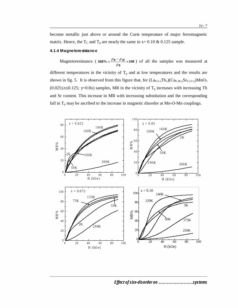
7
Effect of size-disorder on ………………………..systems
become metallic just above or around the Curie temperature of major ferromagnetic
matrix. Hence, the TC and Tp are nearly the same in x= 0.10 & 0.125 sample.
4.1.4 Magnetoresistance
Magnetoresistance ( 100%0
0 ×−
=ρ
ρρ HMR ) of all the samples was measured at
different temperatures in the vicinity of Tp and at low temperatures and the results are
shown in fig. 5. It is observed from this figure that, for (La0.5-xTbx)(Ca0.38-ySr0.12+y)MnO3
(0.025≤x≤0.125; y=0.8x) samples, MR in the vicinity of Tp increases with increasing Tb
and Sr content. This increase in MR with increasing substitution and the corresponding
fall in Tp may be ascribed to the increase in magnetic disorder at Mn-O-Mn couplings.
0 20 40 60 80 10 00
20
40
60
80 x = 0 .0 2 5
1 0 0 K2 K
1 6 0 K
5 0 K
3 0 0 K
1 9 0 K
MR
%
H (kO e ) 0 2 0 4 0 6 0 8 0 1 0 00
2 0
4 0
6 0
8 0
1 0 0x = 0 .05
1 60 K1 00 K
5 0K
1 90 K
2 K
3 00 K
MR
%
H (kO e)
0 20 40 60 80 1000
20
40
60
80
100 x = 0.0 7 5
2 0 0K2K
5 0K
1 3 5K7 5K
MR
%
H (kO e)
0 20 40 60 80 1000
20
40
60
80
100x = 0.10
250K
175K
5K
50K
140K
120K
MR
%
H (kOe)
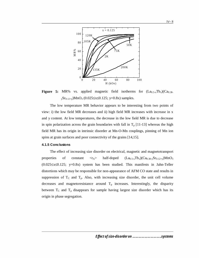
8
Effect of size-disorder on ………………………..systems
0 20 40 60 80 10 00
20
40
60
80
10 0x = 0.1 25
20 0K
50 K10 5K
2K
12 0K
75 K
13 5K
MR
%
H (kO e)
Figure 5: MR% vs. applied magnetic field isotherms for (La0.5-xTbx)(Ca0.38-
ySr0.12+y)MnO3 (0.025≤x≤0.125; y=0.8x) samples.
The low temperature MR behavior appears to be interesting from two points of
view: i) the low field MR decreases and ii) high field MR increases with increase in x
and y content. At low temperatures, the decrease in the low field MR is due to decrease
in spin polarization across the grain boundaries with fall in Tp [11-13] whereas the high
field MR has its origin in intrinsic disorder at Mn-O-Mn couplings, pinning of Mn ion
spins at grain surfaces and poor connectivity of the grains [14,15].
4.1.5 Conclusions
The effect of increasing size disorder on electrical, magnetic and magnetotransport
properties of constant <rA> half-doped (La0.5-xTbx)(Ca0.38-ySr0.12+y)MnO3
(0.025≤x≤0.125; y=0.8x) system has been studied. This manifests in Jahn-Teller
distortions which may be responsible for non-appearance of AFM CO state and results in
suppression of TC and Tp. Also, with increasing size disorder, the unit cell volume
decreases and magnetoresistance around Tp increases. Interestingly, the disparity
between TC and Tp disappears for sample having largest size disorder which has its
origin in phase segregation.
9
Effect of size-disorder on ………………………..systems
4.2 Electrical and magnetic properties of largely hole-doped
(LaR)0.55(CaSr)0.45MnO3 compounds
The divalent cation doped manganite systems exhibit largest TC and Tp for
optimal amount (33%) of divalent cation at A-site [2]. When the amount of divalent
cation increases from optimal amount to half-doping, the columbic electrostatic repulsive
interactions between the carriers increases and hence the mobility of carriers decreases.
This has adverse impact on TC and Tp [2]. While approaching the half-doping, the
columbic interactions overcome the kinetic energy of the carriers resulting in an
insulating-antiferromagnetic state [1,2]. Other than this impact of carrier density and
tolerance factor, the effect of size-disorder on the electronic and magnetic behavior has
been very well understood for optimal doped and half doped compounds [1-7]. However,
the effect of size-disorder in the intermediate concentrations of optimal and half-doping
has not been investigated. During this study we have investigated the effect of size-
disorder on the electronic and magnetic behavior of a 45% divalent doped series of
compounds. The size-disorder has been varied by keeping average A-site cation radius
constant (~1.205Å). We have made an interesting choice of magnetic and non-magnetic
rare-earth cations to create disorder at A-site. A series of compounds
(LaR)0.55(CaSr)0.45MnO3 (R=Nd, Sm, Gd, Tb & Y) with different combination of
occupancies of La and doped- rare earth cations. Five different compositions
(La0.25Nd0.3)(Ca0.3Sr0.15)MnO3 (LaGd), (La0.37Sm0.18)(Ca0.3Sr0.15)MnO3 (LaSm),
(La0.41Gd0.14)(Ca0.3Sr0.15)MnO3 (LaGd), (La0.43Tb0.12)(Ca0.3Sr0.15)MnO3 (LaTb),
(La0.45Y0.1)(Ca0.3Sr0.15)MnO3 (LaY) have been studied in detail for structural, electronic,
magnetic and magnetotransport properties. To elucidate the effect of size-disorder
precisely in the compounds, the size-disorder has been varied by small margins. Also, to
make an analogy and comparative study with reported studies, the average A-site cation
radius (~1.205 Å) has been kept constant and nearly same that of standard
La0.55Ca0.45MnO3 (~1.2 Å).
Synthesis
Five polycrystalline samples of (LaR)0.55(CaSr)0.45MnO3 (R=Nd, Sm, Gd, Tb & Y)
were synthesized using solid state reaction method. Dried powders of La2O3, Nd2O3,
Sm2O3, Gd2O3, Tb2O3, Y2O3, CaCO3, SrCO3 and MnO2 were mixed in stoichiometric
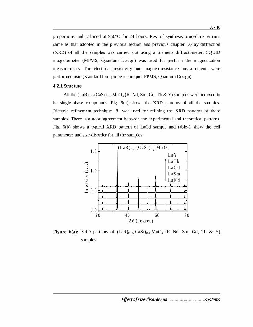
10
Effect of size-disorder on ………………………..systems
proportions and calcined at 950°C for 24 hours. Rest of synthesis procedure remains
same as that adopted in the previous section and previous chapter. X-ray diffraction
(XRD) of all the samples was carried out using a Siemens diffractometer. SQUID
magnetometer (MPMS, Quantum Design) was used for perform the magnetization
measurements. The electrical resistivity and magnetoresistance measurements were
performed using standard four-probe technique (PPMS, Quantum Design).
4.2.1 Structure
All the (LaR)0.55(CaSr)0.45MnO3 (R=Nd, Sm, Gd, Tb & Y) samples were indexed to
be single-phase compounds. Fig. 6(a) shows the XRD patterns of all the samples.
Rietveld refinement technique [8] was used for refining the XRD patterns of these
samples. There is a good agreement between the experimental and theoretical patterns.
Fig. 6(b) shows a typical XRD pattern of LaGd sample and table-1 show the cell
parameters and size-disorder for all the samples.
2 0 4 0 6 0 8 00 .0
0 .5
1 .0
1 .5(L a R )
0 .5 5(C a S r)
0 .4 5M n O
3
L a YL a T bL a G dL a S mL a N d
Inte
nsit
y (a
.u.)
2 θ (d e g re e )
Figure 6(a): XRD patterns of (LaR)0.55(CaSr)0.45MnO3 (R=Nd, Sm, Gd, Tb & Y)
samples.

11
Effect of size-disorder on ………………………..systems
2 0 4 0 6 0 8 0
0 .0
0 .5
1 .0
(L a0.41
G d0.14
) (C a0.3
S r0.15
)M n O3
E x p e r im e n ta l R e f in e d D if fe re n c e B ra g g p e a k
Inte
nsit
y (a
.u.)
2 θ (d eg re e )
Figure 6(b): A typical Rietveld refined pattern for (LaR)0.55(CaSr)0.45MnO3 (R=Gd)
sample.
Table -3: Cell parameters (a,b&c), cell volume (V), average A-site cation radius (<rA),
size-disorder (σ2) for (LaR)0.55(CaSr)0.45MnO3 system.
Sample a (Å) b (Å) c (Å) V (Å3) <rA> (Å) σ2 (Å2)
LaNd 5.438(1) 7.679(1) 5.451(1) 227.62 1.204 0.0023
LaSm 5.444(1) 7.684(1) 5.445(1) 227.77 1.204 0.0029
LaGd 5.449(1) 7.686(1) 5.452(1) 228.33 1.204 0.0032
LaTb 5.451(1) 7.689(1) 5.452(1) 228.50 1.205 0.0034
LaY 5.448(1) 7.685(1) 5.455(1) 228.39 1.205 0.0036
It is seen from table-3 that there is no particular trend observed for the cell
parameters of these sample and cell volumes differ by a very small margins. This may be
attributed to the fact that all the samples have constant average A-site cation radius.
4.2.2 Electronic transport
The electrical resistivity of all the samples was measured in the temperature range
of 5 K- 320 K in 0 T and an applied magnetic field of 5 T. Fig. 7 shows the resistivity
versus temperature plots of all the samples. We see that the I-M transition temperature
starts decreasing with increasing size-disorder. The LaNd sample shows maximum Tp ~
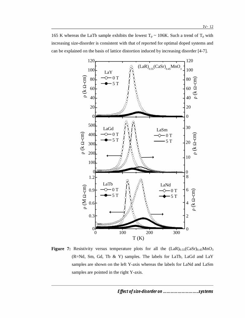
12
Effect of size-disorder on ………………………..systems
165 K whereas the LaTb sample exhibits the lowest Tp ~ 106K. Such a trend of Tp with
increasing size-disorder is consistent with that of reported for optimal doped systems and
can be explained on the basis of lattice distortion induced by increasing disorder [4-7].
0 100 200 3000
0.3
0.6
0.9
1.2
0
2
4
6
80
10
20
30
LaTb 0 T 5 T
ρ (k
Ω-c
m)
ρ (M
Ω-c
m)
T (K)
0
20
40
60
80
100
120
0
20
40
60
80
100
120(LaR)
0.55(CaSr)
0.45MnO
3
LaY 0 T 5 T
ρ (k
Ω-c
m)
ρ (k
Ω-c
m)
ρ (k
Ω-c
m)
ρ (k
Ω-c
m)
0
100
200
300
400
500 LaGd
0 T 5 T
LaNd 0 T 5 T
LaSm 0 T 5 T
Figure 7: Resistivity versus temperature plots for all the (LaR)0.55(CaSr)0.45MnO3
(R=Nd, Sm, Gd, Tb & Y) samples. The labels for LaTb, LaGd and LaY
samples are shown on the left Y-axis whereas the labels for LaNd and LaSm
samples are pointed in the right Y-axis.

13
Effect of size-disorder on ………………………..systems
Interesting feature of I-M transition in these samples is that as Tp decreases the
sharpness of I-M transition increases. This feature may quantified by a quantity called
temperature coefficient of resistance (TCR) [10] given by TCR = (dR/dT)/R×100.
We have calculated this quantity for all the samples and have been shown in fig. 8.
0 100 200 300-10
-5
0
5
10
15
TC
R
T (K)
Tb Eu
-80
-40
0
40
80
T
CR
Y Gd
-8
-4
0
4
8
12
T
CR
Nd Sm
Figure 8: Temperature coefficient of resistance (TCR) versus temperature plots for all
the (LaR)0.55(CaSr)0.45MnO3 (R=Nd, Sm, Gd, Tb & Y) samples (Here LaEu
sample has been taken from chapter 3).
The large values of TCR are desirable for bolometric applications. A larger
variation of resistance in the vicinity Tp is a signature of such a property in these
samples. We note that as size-disorder increases, Tp increases and the peak resistivity
increases drastically. This results a larger TCR in the vicinity of Tp. Earlier a large TCR
has been reported to occur in thin films [16-18]. Our attempt to focus this property in
these samples shows that a large TCR can occur in polycrystalline bulk samples too.

14
Effect of size-disorder on ………………………..systems
4.2.3 Magnetic properties
The Zero-field-cooled (ZFC) and field-cooled (FC) magnetization measurements
on all the (LaR)0.55(CaSr)0.45MnO3 (R=Nd, Sm, Gd, Tb & Y) samples were performed
over a temperature range of 5K-330K in an applied magnetic field of 50 Oe. All the
samples exhibit Curie temperature (TC) nearly at same temperature of I-M transition.
0 100 200 3000
3
6
9
H = 50 Oe
LaNd LaTb ZFC ZFC FC FC
M (
emu/
g)M
(em
u/g)
M (
emu/
g)
T (K)
0
2
4
H = 50 Oe
LaSm LaY ZFC ZFC FC FC
0
3
6
9(LaR)
0.55(CaSr)
0.45MnO
3
LaGd ZFC FC
H = 50 Oe
Figure 9: Zero-field-cooled (ZFC) and field-cooled (FC) magnetization (M) versus
temperature (T) plots for all the (LaR)0.55(CaSr)0.45MnO3 (R=Nd, Sm, Gd, Tb
& Y) samples. The magnetization has been acquired in a field of H = 50 Oe.

15
Effect of size-disorder on ………………………..systems
It may be seen from fig. 9 that TC decreases as the size-disorder increases. This
may explained by local structure distortion because of the random displacement of
oxygen ions from their actual crystallographic positions. Also, it may be noted that there
is a large bifurcation between the ZFC and FC magnetization curves. This shows the spin
response when cooled in an applied magnetic field. These samples are heavily doped
and, therefore, more spin disorder exists. Cooling in an applied field causes more spin
ferromagnetic order and hence a larger bifurcation between ZFC and FC curves. The
magnetization data was also acquired in an applied field of H = 5 kOe in ZFC manner.
The inverse susceptibility versus temperature (in a field H = 5kOe) are plotted in fig. 10.
0 100 200 3000
2
4 H = 5 kOe
H/M
(O
e-g/
kem
u)
T (K)
LaNd LaGd
0
2
4H = 5 kOe
LaSm LaTb
0
2
4
H = 5 kOe
(LaR)0.55
(CaSr)0.45
MnO3
LaY
Figure 10: Inverse Susceptibility (H/M) versus temperature (T) plots for all
(LaR)0.55(CaSr)0.45MnO3 (R=Nd, Sm, Gd, Tb & Y) samples. The
magnetization has been acquired in a field of H = 50 Oe.

16
Effect of size-disorder on ………………………..systems
0 10 20 30 40 500
30
60
90
5 K
300 K
300 K
LaNd
M (
emu
/g)
M (
emu
/g)
M (
emu
/g)
M (
emu
/g)
M (
emu
/g)
T (K)
0
30
60
905 K
LaSm
0
30
60
90 5 K
300 K
LaGd
0
30
60
905 K
300 K
LaTb
0
30
60
90
(LaR)0 .55
(CaSr)0 .45
MnO3
5 K
300 K LaY
Figure 11: Magnetization (M) versus field (H) isotherms for (LaR)0.55(CaSr)0.45MnO3
(R=Nd, Sm, Gd, Tb & Y) samples at temperatures of 5 K and 300 K.
Figure 10 depicts inverse susceptibility versus temperature for all the samples. It
may be seen that there is a large deviation in Curie-Weiss behavior from magnetic
susceptibility for all the samples. This indicates towards the inhomogeneous magnetic
nature near the Curie point. This points towards the segregation of the small
ferromagnetic phases in the paramagnetic matrix. Since these samples have a large size-

17
Effect of size-disorder on ………………………..systems
disorder, therefore, it is quite likely that phase segregation takes place and influence the
electrical and magnetic properties. The magnetization versus field isotherms were
recorded for all the samples both in the low temperature ferromagnetic region and room
temperature paramagnetic region and are shown in fig. 11. It may be seen from the figure
that there is no spontaneous magnetization at a temperature of 300 K for all these
samples whereas all the samples exhibit a saturated ferromagnetism at 5K. We have
calculated the spin only saturation magnetization values using the relation SgM Bµ=
and found that the experimental saturation values are in a good agreement with those of
the calculated ones. The values of experimental and theoretical magnetization along with
the Curie points and I-M transition temperatures for all the samples are given in table-4.
Table-4: Curie temperature (TC), insulator-metal transition (Tp), theoretical and
experimental saturation magnetization (MS) values for
(LaR)0.55(CaSr)0.45MnO3 (R=Nd, Sm, Gd, Tb & Y) samples.
R Tp(K) TC(K) MS(exp) (µB) MS(cal)(µB)
Nd 167 170 3.31 3.55
Sm 140 140 3.32 3.55
Gd 130 125 3.90 3.55
Tb 120 120 3.59 3.55
Y 119 120 3.49 3.55
It may also be seen from table – 4 that for the samples having magnetic rare-earth
ion as a substituent, the experimental saturation magnetization values exceed the
theoretical values. LaGd sample has the maximum deviation followed by LaTb and
LaNd samples. This is attributed to the addition the paramagnetic moments to spin only
magnetization saturation values.
4.2.4 Magnetoresistance properties
Figure 12 shows the MR% versus field isotherms at different temperatures in the
vicinity of Tp and at low temperatures for all the (LaR)0.55(CaSr)0.45MnO3 (R=Nd, Sm,
Gd, Tb & Y) samples.
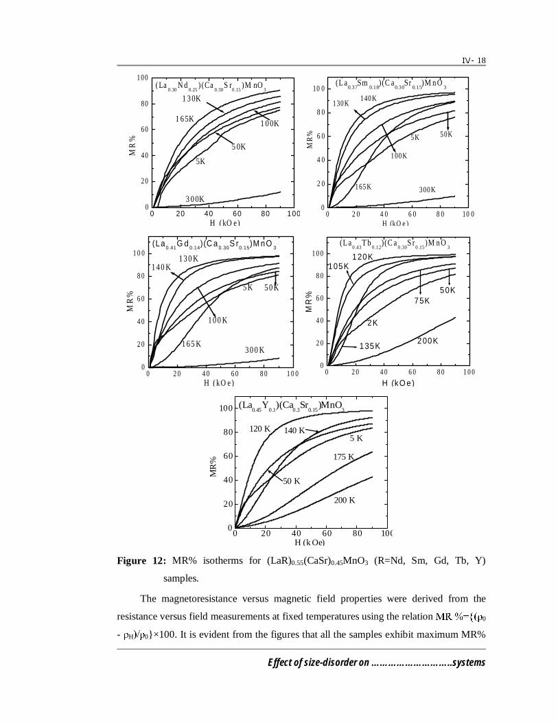
18
Effect of size-disorder on ………………………..systems
0 20 40 60 80 1000
20
40
60
80
100
(La0.30
N d0.25
) (Ca0.30
S r0.15
)M nO3
1 6 5K
3 0 0K
1 0 0K
1 3 0K
5 0K
5K
MR
%
H (kO e) 0 2 0 4 0 6 0 8 0 10 0
0
2 0
4 0
6 0
8 0
10 0
(L a0.37
Sm0.18
)(C a0.30
Sr0.15
)M n O3
165K
100K
50K5K
300K
130K140K
MR
%
H (kO e )
0 2 0 4 0 6 0 8 0 1 0 00
2 0
4 0
6 0
8 0
1 0 0(La
0.41G d
0.14)(C a
0.30S r
0.15)M nO
3
1 4 0 K
3 0 0 K
5 0 K5 K
1 0 0 K
1 6 5 K
1 3 0 K
MR
%
H (kO e ) 0 2 0 4 0 6 0 8 0 1 0 0
0
2 0
4 0
6 0
8 0
1 0 0
(L a0.43
T b0.12
)(C a0.30
S r0.15
)M n O3
200K135K
105K
2K
50K75K
120K
MR
%
H (kO e)
0 20 40 60 80 1000
20
40
60
80
100 (La0.45
Y0.1
)(Ca0.3
Sr0.15
)MnO3
50 K
120 K
175 K
140 K
200 K
5 K
MR
%
H (k Oe)
Figure 12: MR% isotherms for (LaR)0.55(CaSr)0.45MnO3 (R=Nd, Sm, Gd, Tb, Y)
samples.
The magnetoresistance versus magnetic field properties were derived from the
resistance versus field measurements at fixed temperatures using the relation 0
- H0×100. It is evident from the figures that all the samples exhibit maximum MR%
19
Effect of size-disorder on ………………………..systems
in the vicinity of Tp. The MR% increases as the temperature decreases, possibly due to
increase in the spin polarization [11-13]. However, the MR behavior at low and high
fields shows interesting trends. In the systems with high Tp values (>200K), at low
temperatures, the high field (>1 Tesla) MR is very low as compared to low field (<1
Tasla) MR. In the present samples under investigation, the high field is very large and is
3-4 orders larger than low field MR. In these samples, it is seen in MR isotherms at 5K
that low field MR is nearly 20% whereas high field MR is around 60%, which is
extremely large value at a temperature when spin polarization is almost complete. The
complete spin polarization of 3d band of Mn ions is also evident from the saturation
magnetization values calculated from the M-H isotherms (fig. 11) [11-13]. There is a
nice agreement of experimental saturation magnetization values agree with those
calculated from spin only values at very low magnetic fields (<1 Tesla). Hence, the
saturation magnetization in low fields at 5K point towards the complete spin
polarization. This can be related with the explanation of low and high field MR at low
temperatures. The high field MR generally originates from spin magnetic disorder at Mn-
O-Mn bonds when the spin polarization is not complete. However, the nearly complete
spin polarization in these samples rules out the above cause responsible for high field
MR. Now, this high field MR may have its origin in extrinsic factor such as connectivity
between the grains, pinning of Mn ion spins at the grain boundaries and contamination at
grain surfaces. The possibility of spin cluster glass behavior too cannot be ruled out since
the large size-disorder has a tendency towards the formation spin cluster glass behavior.
There are also few reports on the segregation of microscopic insulating phases at the
grain boundaries in such samples with large size-disorder at A-site. Therefore, the
possibility cause of high field MR at low temperatures lies in any of the above extrinsic
factors. However, the detailed investigations of a cause among all given above have been
left for the future studies.
4.2.5 Conclusions
The structural, electrical, magnetic and magnetoresistive properties of
(LaR)0.55(CaSr)0.45MnO3 (R=Nd, Sm, Gd, Tb & Y) samples have been studied. It is
found that all these samples crystallize in a distorted orthorhombic structure. These
samples have nearly same average A-site cationic radius as that of La0.55Ca0.45MnO3
(LCMO). However, the large size disorder is very large as compared to LCMO.
20
Effect of size-disorder on ………………………..systems
Therefore, these samples exhibit very low TP in the vicinity 125K. The magnetization
saturates at a temperature of 5K and experimental values of saturation magnetization
agree well with those of calculated ones. A large MR of 90%-100% is observed for all
the samples in the vicinity of Tp. At low temperature of 5K, the MR% ~ 90% in which
the low field MR is as a result of spin polarized tunneling whereas high field MR is
attributed to the various possible extrinsic effects.
21
Effect of size-disorder on ………………………..systems
REFERENCES
1. C.N.R. Rao, A.K. Cheetam, Chem. Mater. 10, 2714 (1998).
2. “Colossal magnetoresistance” ed. by C.N.R. Rao and B. Raveau, World
Scientific Publishing Company (1998).
3. P.V. Vanitha, P.N. Santhosh, R.S. Singh, C.N.R. Rao, J.P. Attfield, Phys. Rev. B
59, 13539 (1999).
4. Y.Q. Gong, Ian Maclaren, X.F. Duan, Z.H. Wang and B.G. Shen, Appl. Phys.
Lett. 78, 2157 (2001).
5. Y.Q. Gong, Ian Maclaren, X.F. Duan, Z.H. Wang and B.G. Shen, J. Appl. Phys.
90, 488 (2001).
6. L.M. Rodriguez-Martinez and J.P. Attfield, Phys. Rev. B 54, 15622 (1996).
7. L.M. Rodriguez-Martinez and J.P. Attfield, Phys. Rev. B 58, 2426 (1998).
8. J. Rodriguez_Carvajel, FULLPROF version 3.0 Laboratorie Leon Brillioun,
CEA-CNRS, (1995).
9. Hirotoshi Terashita and J.J. Neumeirer, Phys. Rev. B 63, 174436 (2001).
10. Young Sun, M.B. Salamon, Wei Tong and Yuheng Zhang, Phys. Rev. B 66,
94414 (2002)
11. H.Y. Hwang, S.-W. Cheong, P.G. Radaelli, M. Marezio and B. Batlogg, Phys.
Rev. Lett. 75, 914 (1995).
12. A. Gupta, G. Q. Gong, G. Xiao, P. R. Duncombe, P. Lecoeur, P. Trouilloud, Y.
Y. Wang, V. P. Dravid and J. Z. Sun, Phys. Rev. B 54, 15629 (1996).
13. P. Raychaudhuri, K. Sheshadri, S. Bandyopadhyay, P. Ayyub, A.K. Nigam, R.
Pinto, S. Chaudhuri, S.B. Roy, Phys. Rev. B 59, 13919(1999).
14. A. de Andres, M. Garcia-Hernandez, J. L. Martinez, Phys. Rev. B 60, 7328
(1999).
15. A. de Andres, M. Garcia-Hernandez, J. L. Martinez, C. Preito, Appl. Phys Letts
74, 3884 (1999).
16. M. Rajeshwari, C.H. Chen, A. Goyal, C. Kwon, M.C. Robson, R. Ramesh, T.
Venktesan, S. Lakeou, Appl. Phys. Lett. 68, 3555 (1996).
17. M. Rajeshwari, A. Goyal, R. Shreekala, S.E. Lofland, S.M. Bhagat, R. Ramesh,
T. Venktesan, Appl. Phys. Lett. (1998).
22
Effect of size-disorder on ………………………..systems
18. A. Goyal, M. Rajeshwari, R. Shreekala, S.E. Lofland, S.M. Bhagat, T. Boettcher,
C. Kwon, R. Ramesh, T. Venktesan, Appl. Phys. Lett. 71, 1718 (1998).
Chapter – 5
Investigations on low temperature resistivity minimum
in (La0.5Pr0.2)Ba0.3MnO3 polycrystalline bulk and
epitaxial thin films
5.1 Synthesis, structure and surface morphology V-1
5.1.1 Synthesis V-1
5.1.2 Structure V-2
5.1.3 Surface morphology V-3
5.2 Resistivity and magnetization V-5
5.2.1 Resistivity V-5
5.2.2 Magnetization V-8
5.3 Low temperature resistivity minimum V-8
5.4 Magnetoresistance V-15
5.5 Conclusions V-19
References V-21
1
Investigation on low temperature …………………..bulk and epitaxial thin films
In this chapter, the cause and occurrence of low temperature transport anomalies in
polycrystalline bulk and epitaxial thin films of (La0.5Pr0.2)Ba0.3MnO3 have been discussed.
The large size-disorder plays an important role in inducing the local structural strain and
modifies the transport and magnetic properties. Ba2+ is one such large size cation (cation
size~1.47 Å) which induces the local structural distortions [1,2]. In the present chapter, the
discussion is made on the properties of Ba-doped (La0.5Pr0.2)Ba0.3MnO3 (LPBMO)
composition which possesses a large A-site size disorder ~ 0.015 Å2. This sample has been
previously studied in our group in bulk polycrystalline form for its structural, electrical
and magnetic properties. Though there has been enough study on this stoichiometry but
the low temperature transport properties still remain fully unexplored. This sample
exhibits a low temperature minimum around a temperature of 40 K followed by a
resistivity upturn. Such a behavior is rare and not investigated widely in manganites
having large A-site size-disorder. Mainly, there can be three reasons for this kind of
behavior at low temperatures, namely, 1) The grain boundary effect and, 2) the electron-
electron scattering and weak localization at low temperatures and 3) Kondo effect [3-9].
Therefore, to elucidate whether this is a grain boundary effect or one of the other
two, we have synthesized this sample both in polycrystalline and thin film forms. The
studies on epitaxial thin films are interesting to understand the clean physics of crystal
structure in the absence of dominating grain boundary behavior. Keeping this in mind, a
comparative study of polycrystalline bulk and epitaxial thin films has been carried out.
After sufficient experimental evidences and theoretical support, it has been found that the
low temperature resistivity minimum is due to the electron-electron scattering and grain
boundaries do not play any significant role in such kind of behavior.
5.1 Synthesis, structure and surface morphology
5.1.1 Synthesis
Bulk polycrystalline sample of La0.5Pr0.2Ba0.3MnO3 was synthesized by mixing the
constituent oxides and carbonates (La2O3, Pr6O11, MnO2, BaCO3; purity > 99.9%) in
proper stochiometric proportions. The mixture was calcinated at 950ºC for 24 hrs. The
sample was then ground, pelletized and heated at 1100ºC for 40 hrs. The sample was
sintered in the range of 1200ºC – 1300ºC for 100 hrs with several intermittent grindings.
The final sintering was carried out at 1350ºC for 40 hrs. This sample was used for bulk

2
Investigation on low temperature …………………..bulk and epitaxial thin films
characterization as well as for thin film deposition by Pulsed Laser Deposition (PLD)
technique.
The dimensions of the target used for deposition were 15mm diameter and 2mm
thickness. The PLD of thin films was carried out using KrF excimer laser. Thin films of
different thicknesses of 200 nm, 100 nm and 50 nm were deposited using same deposition
parameters. The details of deposition parameters are given below.
Table 1: Thin films deposition parameters.
Laser used KrF excimer
Laser frequency 248 Hz
Pulse width 25 ns
Substrate to target distance 4.2 cm
Substrate heater temperature 830°C
Oxygen partial pressure 400 mTorr
Target used La0.5Pr0.2Ba0.3MnO3
(Diameter – 15mm, thickness – 2mm)
Substrate used Single crystal LaAlO3 (100)
(procured commercially)
The structure of the samples was analyzed using X-ray diffraction (XRD) and
surface morphology was studied using Atomic Forced Microscopy (AFM). The resistivity
was measured as a function of temperature in range of 5K-320K and as a function of
magnetic field recorded as 0T - 9T - (-9T) - 0T using PPMS facility at TIFR, Mumbai. The
magnetization measurements on the thin films in zero-field-cooled (ZFC) and field-cooled
(FC) manner were performed in the temperature range of 5K - 250K using SQUID
magnetometer (Quantum Design) at TIFR, Mumbai
5.1.2 Structure
Indexing of XRD patterns of (La0.5Pr0.2)Ba0.3MnO3 polycrystalline bulk sample
reveals that sample crystallizes in a distorted orthorhombic structure (space group: Pnma,
no. 62). Fig. 1 shows the Rietveld refined XRD pattern of the sample showing that there is
a good agreement between fitted and experimental patterns.

3
Investigation on low temperature …………………..bulk and epitaxial thin films
Figure 1: A typical XRD pattern for (La0.5Pr0.2)Ba0.3MnO3 bulk sample.
Figure 2 shows a typical XRD pattern of thin film having 200 nm of thickness
deposited on LaAlO3 (LAO) single crystal substrate. The XRD pattern of the thin film was
indexed using the refined cell parameters of the bulk sample and was found to be single-
phase and (101) direction oriented.
20 30 40 50 60 700
5
10
15
20
25
20 2
10 1
10 0(L A O )
20 0(L A O )
Inte
nsi
ty (
a.u
.)
2θ (d egr ee )
LP B M O2 00nm
Figure 2: A typical XRD pattern for (La0.5Pr0.2)Ba0.3MnO3 200 nm thin film.
5.1.3 Surface morphology
The surface of all the (La0.5Pr0.2)Ba0.3MnO3 thin film with thickness of 200nm,
100nm and 50nm was probed and studied using Atomic Forced Microscopy (AFM)
working on the principle of contact-mode. The micrographs are shown below.

4
Investigation on low temperature …………………..bulk and epitaxial thin films
Picture 1: Transverse and cross-sectional AFM micrographs of 200 nm LPBMO thin film.
Picture 2: Transverse and cross-sectional AFM micrographs of 100 nm LPBMO thin film.
Picture 3: Transverse and cross-sectional AFM micrographs of 50 nm LPBMO thin film.

5
Investigation on low temperature …………………..bulk and epitaxial thin films
The pictures 1-3 show the transverse and cross-sectional views of AFM micrographs
of thin films of different thicknesses of 200nm, 100nm and 50nm respectively. The films
have a smooth surface with a bare roughness of ~ 1 nm for all the thicknesses. Also the
grain size varies marginally in the range of 50nm - 70nm.
5.2 Resistivity and magnetization
5.2.1 Resistivity
Figure 3(a) shows the resistivity versus temperature plot of the La0.5Pr0.2Ba0.3MnO3
bulk polycrystalline sample in a temperature range of 5K-300K in different applied fields
of 0T, 3T and 5T and fig. 3(b) shows the magnified part of the resistivity at low
temperatures to emphasize the minimum in the resistivity. Figs. 4(a&b), 5(a&b) and
6(a&b) show the resistivity versus temperature plots in the temperature range 5K – 320K
and 5K – 100K for thin films of 200nm, 100nm and 50nm respectively.
0 100 200 3000
50
100
150
200
(a)
0 T 3 T 5 T
La0. 5
P r0. 2
B a0. 3
M nO3 ( P olycr ysta llin e)
R (
Ω)
T ( K) 0 2 0 4 0 6 0
5 0
1 0 0
1 5 0( b )
0 T 3 T 5 T
R (
Ω)
T ( K )
Figure 3: (a) Resistivity versus temperature plot for (La0.5Pr0.2)Ba0.3MnO3 bulk sample
and (b) magnified part of the low temperature resistivity minimum.
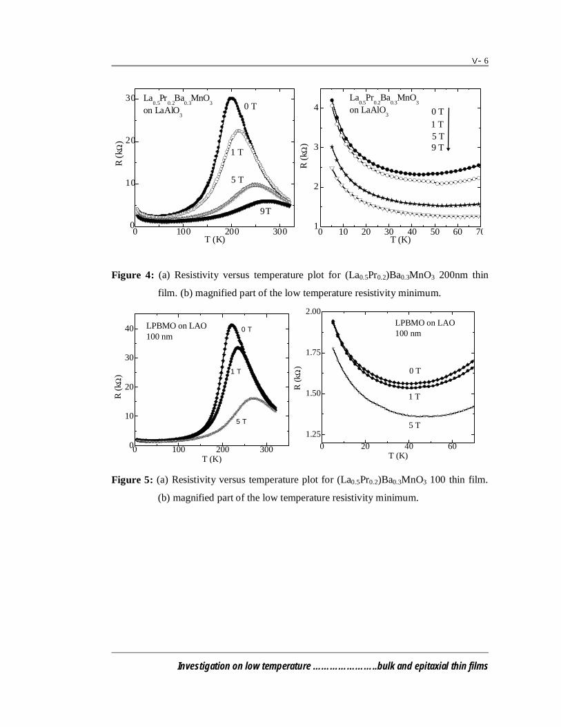
6
Investigation on low temperature …………………..bulk and epitaxial thin films
0 100 200 3000
10
20
30
9T
5 T
1 T
0 TLa
0.5Pr
0.2Ba
0.3MnO
3
on LaAlO3
R (k
Ω)
T (K)
0 10 20 30 40 50 60 701
2
3
4
9 T5 T1 T0 T
La0.5
Pr0.2
Ba0.3
MnO3
on LaAlO3
R (
k Ω)
T (K)
Figure 4: (a) Resistivity versus temperature plot for (La0.5Pr0.2)Ba0.3MnO3 200nm thin
film. (b) magnified part of the low temperature resistivity minimum.
0 100 200 3000
10
20
30
40
5 T
1 T
0 T
R (
k Ω)
T (K)
LPBMO on LAO100 nm
0 20 40 60
1.25
1.50
1.75
2.00
5 T
1 T
0 T
R (
k Ω)
T (K)
LPBMO on LAO100 nm
Figure 5: (a) Resistivity versus temperature plot for (La0.5Pr0.2)Ba0.3MnO3 100 thin film.
(b) magnified part of the low temperature resistivity minimum.
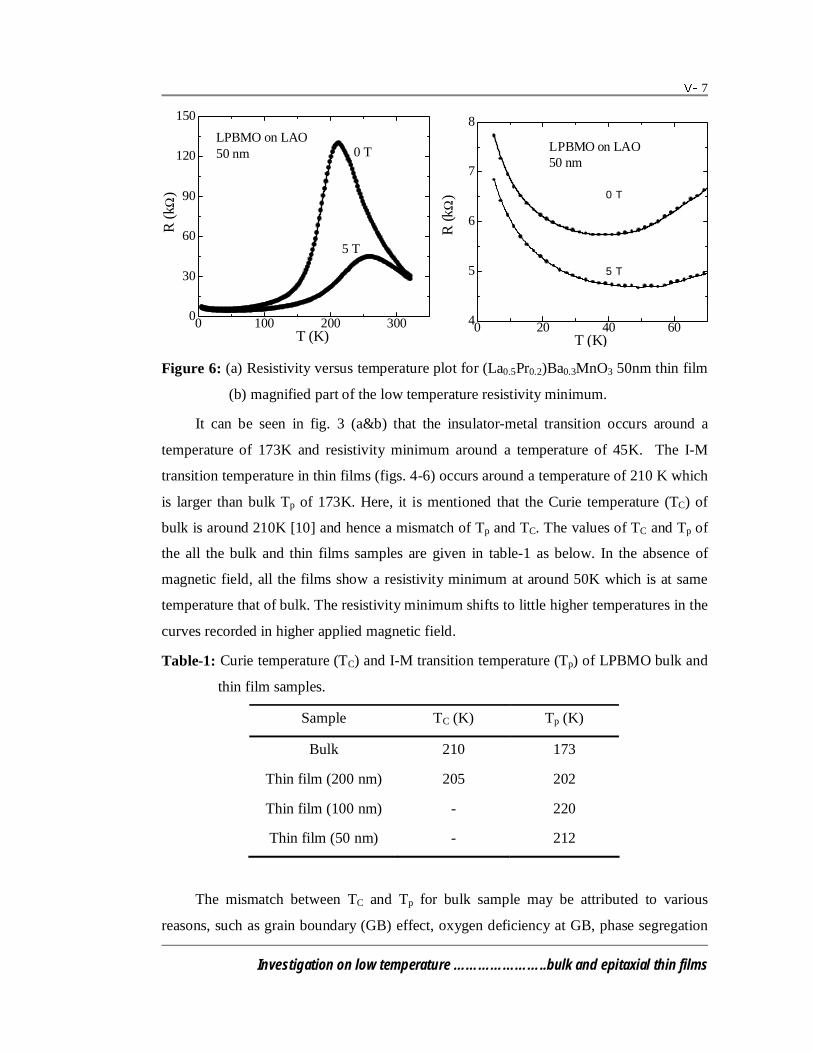
7
Investigation on low temperature …………………..bulk and epitaxial thin films
0 100 200 3000
30
60
90
120
150
5 T
0 T
R (
k Ω)
T (K)
LPBMO on LAO50 nm
0 20 40 604
5
6
7
8
5 T
0 T
R (k
Ω)
T (K)
LPBMO on LAO50 nm
Figure 6: (a) Resistivity versus temperature plot for (La0.5Pr0.2)Ba0.3MnO3 50nm thin film
(b) magnified part of the low temperature resistivity minimum.
It can be seen in fig. 3 (a&b) that the insulator-metal transition occurs around a
temperature of 173K and resistivity minimum around a temperature of 45K. The I-M
transition temperature in thin films (figs. 4-6) occurs around a temperature of 210 K which
is larger than bulk Tp of 173K. Here, it is mentioned that the Curie temperature (TC) of
bulk is around 210K [10] and hence a mismatch of Tp and TC. The values of TC and Tp of
the all the bulk and thin films samples are given in table-1 as below. In the absence of
magnetic field, all the films show a resistivity minimum at around 50K which is at same
temperature that of bulk. The resistivity minimum shifts to little higher temperatures in the
curves recorded in higher applied magnetic field.
Table-1: Curie temperature (TC) and I-M transition temperature (Tp) of LPBMO bulk and
thin film samples.
Sample TC (K) Tp (K)
Bulk 210 173
Thin film (200 nm) 205 202
Thin film (100 nm) - 220
Thin film (50 nm) - 212
The mismatch between TC and Tp for bulk sample may be attributed to various
reasons, such as grain boundary (GB) effect, oxygen deficiency at GB, phase segregation

8
Investigation on low temperature …………………..bulk and epitaxial thin films
near the Curie temperature [11]. However, these effects are almost absent in single
crystalline thin films.
5.2.2 Magnetization
The zero-field-cooled (ZFC) and field-cooled (FC) magnetization of thin film of
thickness ~ 200nm was carried out in a field of 200 Oe in a temperature range of 250K-5K
and is shown below as fig. 7.
0 50 100 150 200 2500
1
2
3
4
5
FC
ZFC
LPBMO on LAO200 nm
H = 200 Oe
M (
10-4em
u)
T (K)
Figure 7: Zero-field-cooled (ZFC) and field-cooled (FC) magnetization vs. temperature
plots for La0.5Pr0.2Ba0.3MnO3 200 nm thin film in a field of 200 Oe.
The curie point of the thin films occurs at ~205K which agrees well with the Tp of
thin films. The TC and Tp of thin films match nicely with each other, thus indicating the
homogenous structure of thin films.
5.3 Low temperature resistivity minimum
Investigation on the evolution of low temperature resistivity minimum in
(La0.5Pr0.2)Ba0.3MnO3 has been the major motivation of this chapter. Though there are few
reports of such behavior but with a divided opinion on its cause [5-8]. Some reports have
been on the resistivity minima in standard La0.7Ca0.3MnO3 and La0.7Sr0.3MnO3 with a
unanimous reason of electron-electron scattering due to the potential fluctuation in the
cores of trivalent and divalent cations experienced by the conduction electrons [5-7].
However, such kind of potential fluctuation is associated with all the divalent cations.
Hence, all manganites should exhibit this behavior in all the structural forms which is not
the case. Also, there are reports of such kind of behavior in La0.5Pb0.5MnO3 compound and

9
Investigation on low temperature …………………..bulk and epitaxial thin films
its origin is reported to occur in grain boundaries [8]. Also, in the literature, no effort has
been made to identify the cause of low temperature resistivity minima in compounds with
large A-site cation size disorder.
Amid all these contrasting and unclear causes of low temperature resistivity minima,
an effort has been made to identify the cause by synthesizing (La0.5Pr0.2)Ba0.3MnO3 both in
bulk polycrystalline and epitaxial single crystalline thin film forms. Thin films of different
thicknesses were deposited because grain size varies with thickness and hence, it is a
probe to investigate whether grain boundary is the cause of low temperature resistivity
minimum. This low temperature anomaly in the resistivity has been resolved by applying
different models.
Let us first evaluate grain boundary as the cause of resistivity minimum. At low
temperature grain boundaries act as insulating barrier to conduction of electrons and hence
may results in abrupt rise in resistivity. Also, the pinning of Mn ion spin creates the
insulating paths which dominate at low temperature. Since the (La0.5Pr0.2)Ba0.3MnO3
sample possesses a large size-disorder, there is large possibility of grain boundary
contamination through pinning of spin at the interfaces and formation of microscopic
insulating phases which act as strong insulating barrier at the interfaces of conducting
grains. However, the grain boundaries can be made metallic on the application of magnetic
fields and the low temperature resistivity minimum can be dissolved [8]. We observe (figs.
3-6) in bulk and thin film samples that the application of magnetic field only suppresses
the net resistivity and doesn’t dissolve resistivity upturn. This shows that grain boundary
does not cause this localization. This is further supported by the fact that with the
decreasing thickness in thin films, the grain size decreases and hence the effective grain
surface area increases. Increasing the grain boundary area with decreasing thickness of
thin films does not show any substantial variation in the nature of low temperature
resistivity minima. Therefore, the fact that the grain size variation by changing the
thickness in the thin films and the effect of magnetic field doesn’t induce any qualitative
modification in resistivity minimum is a striking evidence of grain boundary as not a cause
of such resistivity minimum.
We also take into note that, at low temperatures, Kondo scattering by a magnetic
impurity in a non-magnetic lattice also causes the low temperature resistivity minima. We
10
Investigation on low temperature …………………..bulk and epitaxial thin films
neglect the possibility of this effect because Kondo scattering minimizes on the
application of magnetic field which should result in disappearance of resistivity minima
[3-5]. In our samples, the low temperature resistivity minimum is present in large
magnetic fields too. Also, there is no magnetic impurity in the sample as no secondary
phase is found to exist within the detectable limit of XRD. Therefore, the possibility of
Kondo scattering is ruled out.
The other factor which can be a cause of this behavior is the low temperature
electron-electron scattering due to columbic interactions between charge carriers and the
weak localization. Such kind of scattering is possible when the low temperature resistivity
is more than the Mott’s maximum limit of metallic resistivity of ~ 10 cmmΩ [3-5]. In our
bulk and thin film samples, the resistivity is quite above this limit and hence the electron-
electron elastic scattering is quite plausible factor. It is known that the resistivity in the
metallic region is due to the various electron-phonon and electron-magnon inelastic
scattering processes. This anomalous resistivity in the low temperature region can be
reproduced by adding e-e elastic scattering term to inelastic scattering term as
inelasticelastic ρρρ += - (1)
where elasticρ is the correction to resistivity due to low temperature elastic e-e scattering
and inelasticρ is resistivity term. inelasticρ increases as temperature increases whereas elasticρ is
dominant at low temperatures. The low temperature correction to the resistivity is given by
elasticρ quantified as
2/10
1
BTelastic +
=σ
ρ - (2)
where 0σ is the residual conductivity and B is a constant. Though this law reproduces the
low temperature resistivity rise but there is a deviation near the dip of the minima This can
be attributed to the fact that with increasing temperature the inelastic scattering of
electrons by the phonons and magnons starts dominating the electron-electron (e-e)
scattering (e-e scattering decreases with increasing temperature) and results in the
resistivity minimum. Therefore, a correction to the resistivity can be made by adding a
single power law as describing the inelastic resistivity as
nninelastic Tρρ = - (3)
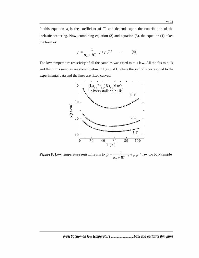
11
Investigation on low temperature …………………..bulk and epitaxial thin films
In this equation nρ is the coefficient of Tn and depends upon the contribution of the
inelastic scattering. Now, combining equation (2) and equation (3), the equation (1) takes
the form as
nnTBT
ρσ
ρ ++
=2/1
0
1 - (4)
The low temperature resistivity of all the samples was fitted to this law. All the fits to bulk
and thin films samples are shown below in figs. 8-11, where the symbols correspond to the
experimental data and the lines are fitted curves.
0 2 0 4 0 6 0 8 0 1 0 0
1 0
2 0
3 0
4 0
5 T
3 T
0 T
(L a0 .5
P r0 .2
)B a0 .3
M n O3
P o ly c ry s ta ll in e b u lk
ρ ( Ω
-cm
)
T ( K )
Figure 8: Low temperature resistivity fits to nnT
BTρ
σρ +
+= 2/1
0
1 law for bulk sample.

12
Investigation on low temperature …………………..bulk and epitaxial thin films
0 3 0 6 0 9 00 .5
1 .0
1 .5
2 .0
2 .5 (L a0.5
P r0.2
)B a0.3
M n O3
T h in f ilm o n L A O2 0 0 n m
5 T
9 T
1 T
0 T
ρ ( Ω
-cm
)
T (K )
Figure 9: Low temperature resistivity fits to nnTBT
ρσ
ρ ++
=2/1
0
1law for 200 nm
LPBMO thin film.
0 2 0 4 0 6 0 8 0 1 0 0
1 .2
1 .5
1 .8
2 .1(L a
0.5P r
0.2)B a
0.3M n O
3
T h in f ilm o n L A O1 0 0 n m
5 T
1 T
0 T
ρ ( Ω
-cm
)
T (K )
Figure 10: Low temperature resistivity fits to nnTBT
ρσ
ρ ++
=2/1
0
1 law for 100 nm
LPBMO thin film.

13
Investigation on low temperature …………………..bulk and epitaxial thin films
0 2 0 4 0 6 0 8 0 1 0 0
1 .2
1 .6
2 .0
2 .4
5 T
0 T
ρ ( Ω
-cm
)
T ( K )
(L a0 .5
P r0 .2
)B a0 .3
M n O3
T h in f i lm o n L A O5 0 n m
Figure 11: Low temperature resistivity fits to nnTBT
ρσ
ρ ++
=2/1
0
1 law for 50 nm
LPBMO thin film.
All the parameters obtained from the fits are given below in table 2. It is evident
from the very low values of 2χ that the resistivity produced using equation (4) agrees
nicely to the experimental resistivity data. The values of 2χ are acceptable but are little
larger for bulk sample, which may be due to minor contributions of the defects and
polycrystalline grain boundaries to the resistivity. In the absence of magnetic field, the
elastic term exponent (n) ~ 2.5 and it decreases on the application of magnetic fields.
Similarly, the low temperature resistivity of the thin films of all the thicknesses has been
nicely reproduced using above relation.
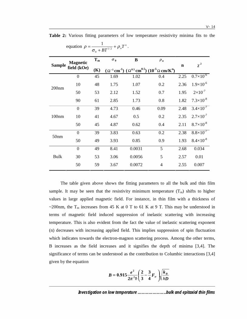
14
Investigation on low temperature …………………..bulk and epitaxial thin films
Table 2: Various fitting parameters of low temperature resistivity minima fits to the
equation nnTBT
ρσ
ρ ++
=2/1
0
1.
Sample Magnetic field (kOe)
Tm
(K)
0σ
( 1−Ω cm-1)
B
( 5.0Ω cm0.5)
nρ
(10-5 Ω cm/Kn) n 2χ
0 45 1.69 1.02 0.4 2.25 0.7×10⁻⁶
10 48 1.75 1.07 0.2 2.36 1.9×10⁻⁶
50 53 2.12 1.52 0.7 1.95 2×10⁻⁷ 200nm
90 61 2.85 1.73 0.8 1.82 7.3×10⁻⁸
0 39 4.73 0.46 0.09 2.48 3.4×10⁻⁷
10 41 4.67 0.5 0.2 2.35 2.7×10⁻⁷ 100nm
50 45 4.87 0.62 0.4 2.11 8.7×10⁻⁸
0 39 3.83 0.63 0.2 2.38 8.8×10⁻⁷ 50nm
50 49 3.93 0.85 0.9 1.93 8.4×10⁻⁸
0 49 8.41 0.0031 5 2.68 0.034
30 53 3.06 0.0056 5 2.57 0.01 Bulk
50 59 3.67 0.0072 4 2.55 0.007
The table given above shows the fitting parameters to all the bulk and thin film
sample. It may be seen that the resistivity minimum temperature (Tm) shifts to higher
values in large applied magnetic field. For instance, in thin film with a thickness of
~200nm, the Tm increases from 45 K at 0 T to 61 K at 9 T. This may be understood in
terms of magnetic field induced suppression of inelastic scattering with increasing
temperature. This is also evident from the fact the value of inelastic scattering exponent
(n) decreases with increasing applied field. This implies suppression of spin fluctuation
which indicates towards the electron-magnon scattering process. Among the other terms,
B increases as the field increases and it signifies the depth of minima [3,4]. The
significance of terms can be understood as the contribution to Columbic interactions [3,4]
given by the equation
D
kF
eB B
−= σπ 4
332
2915.0
2
2

15
Investigation on low temperature …………………..bulk and epitaxial thin films
where F is the screening constant for the coulomb interactions and D is the diffusion
constant.
Increasing the magnetic field causes the depth of minima to increase which also
supports the increase in Tm with magnetic field. This signifies that, at low temperatures,
the e-e scattering term is insensitive to magnetic field whereas the exponent of inelastic
scattering term suppresses largely with increasing magnetic field. Our results agree quite
well with the theoretical predictions of increase in Tm with the applied field. However,
there have been some reports on the decreases of B in higher fields which is beyond the
scope of this law [5]. We don’t observe such anomaly which shows the quality of
agreement between experimental data to theoretical prediction of electron-electron
scattering as the cause of low temperature resistivity minima.
5.4 Magnetoresistance
The magnetoresistance measurements on all the (La0.5Pr0.2)Ba0.3MnO3 bulk and thin
film samples were carried out up to a magnetic field of 9 Tesla both in the vicinity of I-M
transition and at low temperatures. Fig. 12 shows the magnetoresistance (MR%) as a
function of applied magnetic field (H) isotherms for bulk sample at various temperature in
the vicinity and below Tp.
- 90 - 60 - 30 0 30 60 900
20
40
60
80 ( L a0 .5
P r0 .2
) B a0 .3
M n O3 (B u lk p o ly cry s ta l lin e)
MR
%
H (k O e)
T = 5 K T = 1 0 0 K T = 1 7 5 K T = 2 7 5 K
Figure 12: MR% as a function of applied magnetic field for LPBMO bulk sample.
In may be seen from the fig. 12 that, MR% vs. field for bulk sample shows a
maximum ~75% near the I-M transition and decreases as the temperature decreases. At
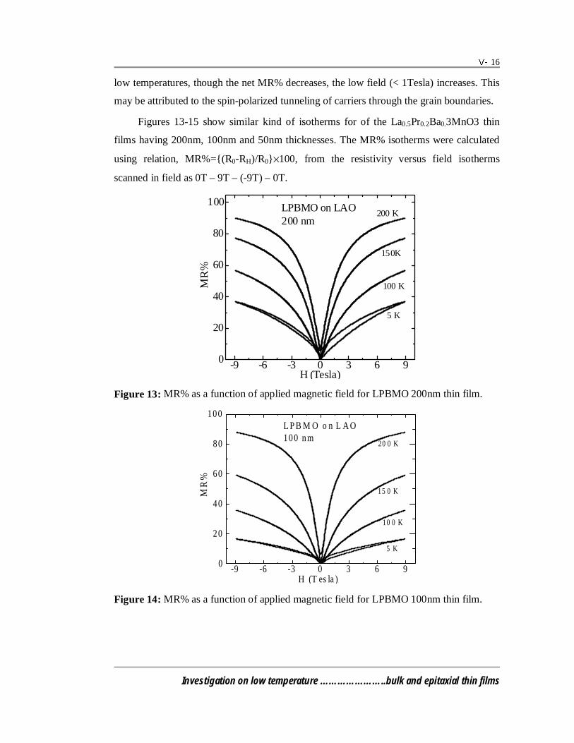
16
Investigation on low temperature …………………..bulk and epitaxial thin films
low temperatures, though the net MR% decreases, the low field (< 1Tesla) increases. This
may be attributed to the spin-polarized tunneling of carriers through the grain boundaries.
Figures 13-15 show similar kind of isotherms for of the La0.5Pr0.2Ba0.3MnO3 thin
films having 200nm, 100nm and 50nm thicknesses. The MR% isotherms were calculated
using relation, MR%=(R0-RH)/R0×100, from the resistivity versus field isotherms
scanned in field as 0T – 9T – (-9T) – 0T.
-9 -6 -3 0 3 6 90
20
40
60
80
100 LPBMO on LAO200 nm
200 K
150K
100 K
5 K
MR
%
H (Tesla)
Figure 13: MR% as a function of applied magnetic field for LPBMO 200nm thin film.
-9 -6 -3 0 3 6 90
20
40
60
80
100
15 0 K
20 0 K
10 0 K
5 K
MR
%
H (T es la )
L P B M O o n L A O100 nm
Figure 14: MR% as a function of applied magnetic field for LPBMO 100nm thin film.
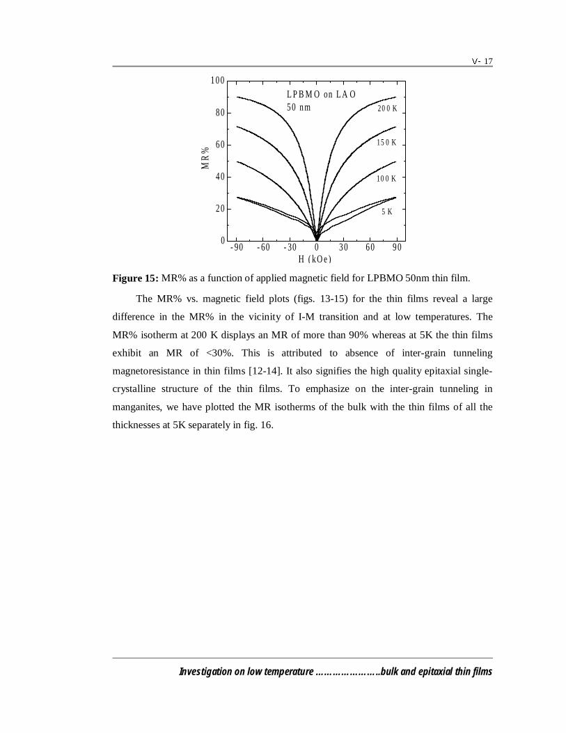
17
Investigation on low temperature …………………..bulk and epitaxial thin films
- 90 - 60 - 30 0 3 0 6 0 9 00
2 0
4 0
6 0
8 0
1 0 0
20 0 K
15 0 K
10 0 K
5 K
L P B M O on L A O5 0 n m
MR
%
H ( k O e )
Figure 15: MR% as a function of applied magnetic field for LPBMO 50nm thin film.
The MR% vs. magnetic field plots (figs. 13-15) for the thin films reveal a large
difference in the MR% in the vicinity of I-M transition and at low temperatures. The
MR% isotherm at 200 K displays an MR of more than 90% whereas at 5K the thin films
exhibit an MR of <30%. This is attributed to absence of inter-grain tunneling
magnetoresistance in thin films [12-14]. It also signifies the high quality epitaxial single-
crystalline structure of the thin films. To emphasize on the inter-grain tunneling in
manganites, we have plotted the MR isotherms of the bulk with the thin films of all the
thicknesses at 5K separately in fig. 16.
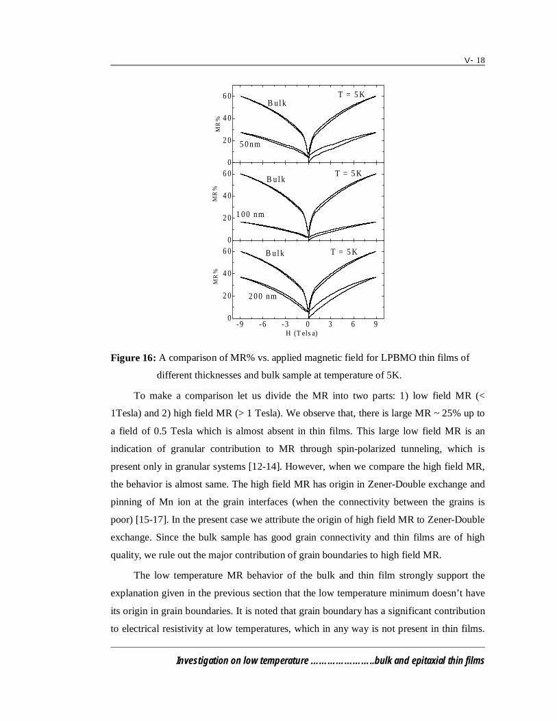
18
Investigation on low temperature …………………..bulk and epitaxial thin films
-9 -6 -3 0 3 6 90
2 0
4 0
6 0 T = 5 KB u l k
2 0 0 n m
MR
%
MR
%
0
2 0
4 0
6 0 T = 5 KB u l k
1 0 0 n m
0
2 0
4 0
6 0 T = 5 K
5 0 n m
B u l k
MR
%
H (T els a)
Figure 16: A comparison of MR% vs. applied magnetic field for LPBMO thin films of
different thicknesses and bulk sample at temperature of 5K.
To make a comparison let us divide the MR into two parts: 1) low field MR (<
1Tesla) and 2) high field MR (> 1 Tesla). We observe that, there is large MR ~ 25% up to
a field of 0.5 Tesla which is almost absent in thin films. This large low field MR is an
indication of granular contribution to MR through spin-polarized tunneling, which is
present only in granular systems [12-14]. However, when we compare the high field MR,
the behavior is almost same. The high field MR has origin in Zener-Double exchange and
pinning of Mn ion at the grain interfaces (when the connectivity between the grains is
poor) [15-17]. In the present case we attribute the origin of high field MR to Zener-Double
exchange. Since the bulk sample has good grain connectivity and thin films are of high
quality, we rule out the major contribution of grain boundaries to high field MR.
The low temperature MR behavior of the bulk and thin film strongly support the
explanation given in the previous section that the low temperature minimum doesn’t have
its origin in grain boundaries. It is noted that grain boundary has a significant contribution
to electrical resistivity at low temperatures, which in any way is not present in thin films.
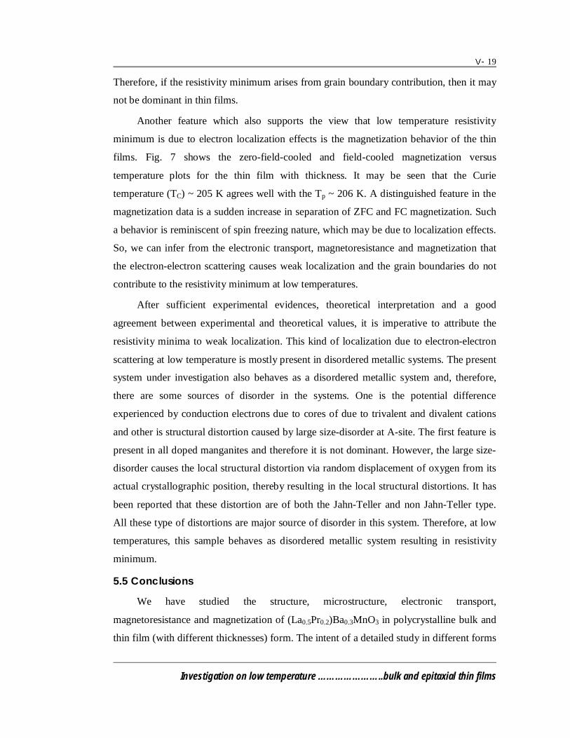
19
Investigation on low temperature …………………..bulk and epitaxial thin films
Therefore, if the resistivity minimum arises from grain boundary contribution, then it may
not be dominant in thin films.
Another feature which also supports the view that low temperature resistivity
minimum is due to electron localization effects is the magnetization behavior of the thin
films. Fig. 7 shows the zero-field-cooled and field-cooled magnetization versus
temperature plots for the thin film with thickness. It may be seen that the Curie
temperature (TC) ~ 205 K agrees well with the Tp ~ 206 K. A distinguished feature in the
magnetization data is a sudden increase in separation of ZFC and FC magnetization. Such
a behavior is reminiscent of spin freezing nature, which may be due to localization effects.
So, we can infer from the electronic transport, magnetoresistance and magnetization that
the electron-electron scattering causes weak localization and the grain boundaries do not
contribute to the resistivity minimum at low temperatures.
After sufficient experimental evidences, theoretical interpretation and a good
agreement between experimental and theoretical values, it is imperative to attribute the
resistivity minima to weak localization. This kind of localization due to electron-electron
scattering at low temperature is mostly present in disordered metallic systems. The present
system under investigation also behaves as a disordered metallic system and, therefore,
there are some sources of disorder in the systems. One is the potential difference
experienced by conduction electrons due to cores of due to trivalent and divalent cations
and other is structural distortion caused by large size-disorder at A-site. The first feature is
present in all doped manganites and therefore it is not dominant. However, the large size-
disorder causes the local structural distortion via random displacement of oxygen from its
actual crystallographic position, thereby resulting in the local structural distortions. It has
been reported that these distortion are of both the Jahn-Teller and non Jahn-Teller type.
All these type of distortions are major source of disorder in this system. Therefore, at low
temperatures, this sample behaves as disordered metallic system resulting in resistivity
minimum.
5.5 Conclusions
We have studied the structure, microstructure, electronic transport,
magnetoresistance and magnetization of (La0.5Pr0.2)Ba0.3MnO3 in polycrystalline bulk and
thin film (with different thicknesses) form. The intent of a detailed study in different forms
20
Investigation on low temperature …………………..bulk and epitaxial thin films
of structure is to elucidate, whether the low temperature resistivity minimum in this
sample is an intrinsic crystal structure property or is a grain boundary property. After
appropriate modeling of low temperature resistivity data of all the bulk and thin films
samples, we conclude that
1. The resistivity minimum manifests in similar kind of nature in both the bulk and
thin film forms (200nm, 100nm & 50nm).
2. The resistivity minimum doesn’t disappear on the application of magnetic field (up
to 9 Tesla). Magnetic field only causes a substantial change in resistance (which is
magnetoresistive characteristic of manganites) and not any significant change in its
behavior.
3. The Tm shift to higher temperature in large applied fields which signifies the
magnetic field suppression of inelastic scattering contribution to resistivity.
4. There is large granular contribution of the bulk sample to MR but absent in case of
thin films.
5. There is a sudden increase in bifurcation of ZFC and FC below Tm which indicates
the spin-freezing like behavior due to carrier localization effect.
On the basis of all these observations and reviewing both the possibilities of
electron-electron scattering and grain boundary effect, we conclude that the former factor
is responsible for such a behavior. The origin of such a behavior lies in the presence of
disorder in the crystal structure (more generally called the disorder metallic system). In
present case, we conclude that large size-disorder at A-site causes the local structural
distortions and is a major of disorder in this low temperature metallic system. To sum up,
the large size-disorder at A-site causes the weak localization of carriers resulting in the
appearance of low temperature resistivity minimum.

21
Investigation on low temperature …………………..bulk and epitaxial thin films
REFERENCES
1. L.M. Rodriguez-Martinez and J.P. Attfield, Phys. Rev. B 54, 15622 (1996).
2. L.M. Rodriguez-Martinez and J.P. Attfield, Phys Rev. B 58, 2426 (1998).
3. B.L. Altshuler, A.G. Aronov, in: A. L. Efros, M. Pollak (Eds.), Electron-Electron
Interactions in Disordered Systems, North Holland, Amsterdam, 1985.
4. P.A. Lee, T.V. Ramakrishnan, Rev. Mod. Phys. 57, 287 (1985).
5. D. Kumar, J. Sankar, J. Narayan, Rajiv K. Singh, A.K. Majumdar, Phys. Rev. B
65, 94407 (2002).
6. A. Tiwari, K.P. Rajeev, Solid State Commun. 111, 33(1999).
7. M. Auslender, A.E. Karkin, E. Rosenberg, G. Gorodetsky, J. Appl. Phys. 89, 6639
(2001).
8. E. Rosenberg, M. Auslender, I. Felner, G. Gorodetsky, J. Appl. Phys. 88, 2578
(2000).
9. P. Raychaudhuri et al., cond-mat/9805320 (unpublished).
10. Ph.D. thesis of K.R. Mavani.
11. Hirotoshi Terashita and J.J. Neumeirer, Phys. Rev. B 63, 174436 (2001).
12. H.Y.Hwang, S.-W. Cheong, P.G. Radaelli, M. Marezio and B. Batlogg, Phys. Rev.
Lett. 75, 914 (1995).
13. A. Gupta, G. Q. Gong, G. Xiao, P. R. Duncombe, P. Lecoeur, P. Trouilloud, Y. Y.
Wang, V. P. Dravid and J. Z. Sun, Phys. Rev. B 54, 15629 (1996)
14. H. Y. Hwang, S.-W Cheog, N. P. Ong, and B. Batlogg, Phys. Rev. Lett. 77, 2041
(1996)
15. H. L. Ju, Hyunchul Sohn, Solid State Commun. 102, 463 (1997).
16. A. de Andres, M. Garcia-Hernandez, J. L. Martinez, C. Preito, Appl. Phys Letts 74,
3884 (1999).
17. A. de Andres, M. Garcia-Hernandez, J. L. Martinez, Phys. Rev. B 60, 7328
(1999).
![[etheses.saurashtrauniversity.edu]etheses.saurashtrauniversity.edu/534/1/dodiya_bl_thesis... · 2012-06-03 · Gram: UNIVERSITY Phone: (R) 0281-2584221 Fax: 0281-2577633 (O) 0281-2578512](https://img.pdfslide.net/doc/110x75/5b606ffe7f8b9ac1478bcbc4/-2012-06-03-gram-university-phone-r-0281-2584221-fax-0281-2577633.jpg)


![Dopant Diffusion – physics [Repaired]](https://img.pdfslide.net/doc/110x75/577d20d41a28ab4e1e93db83/dopant-diffusion-physics-repaired.jpg)