Embed Size (px)
Citation preview
ExhibitionGuide
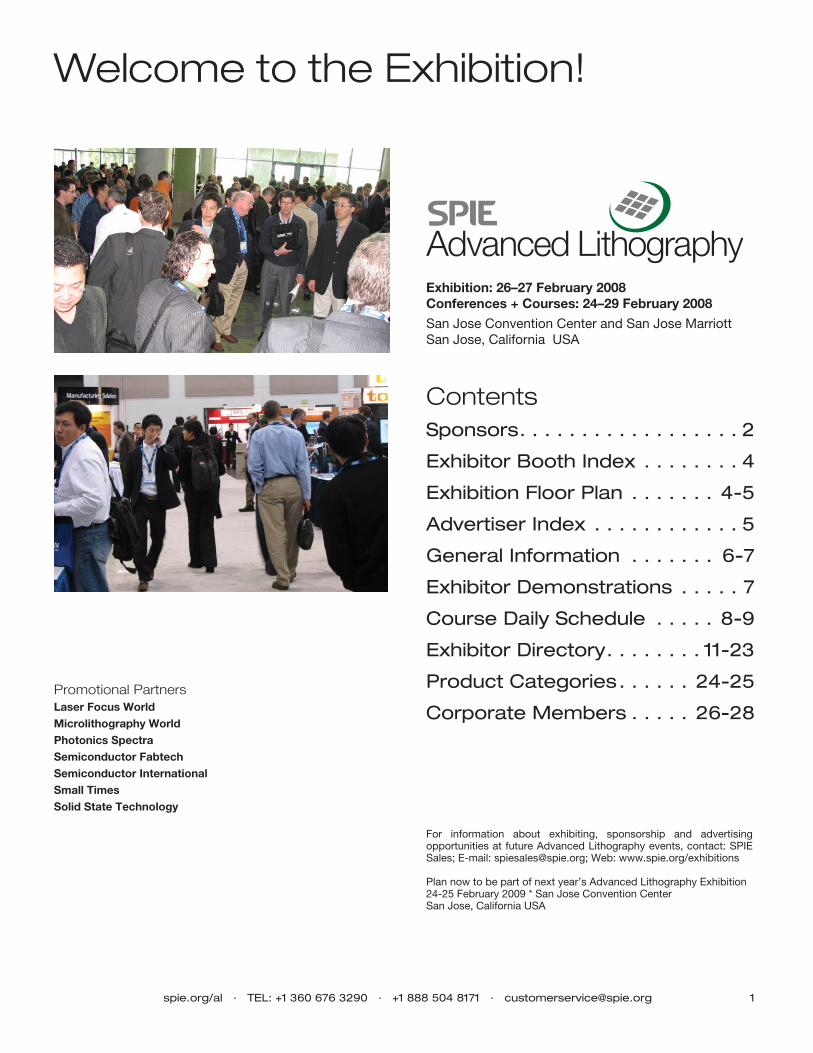
Exhibition: 26–27 February 2008Conferences + Courses: 24–29 February 2008
San Jose Convention Center and San Jose Marriott San Jose, California USA
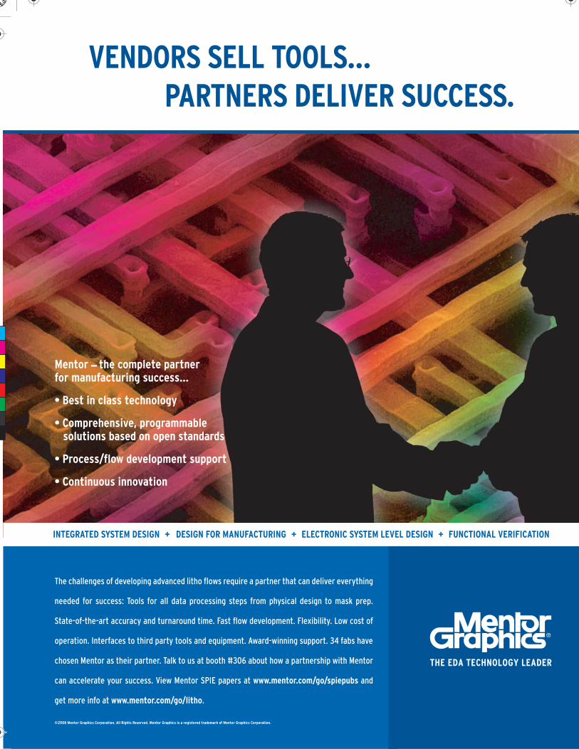
The challenges of developing advanced litho flows require a partner that can deliver everything
needed for success: Tools for all data processing steps from physical design to mask prep.
State-of-the-art accuracy and turnaround time. Fast flow development. Flexibility. Low cost of
operation. Interfaces to third party tools and equipment. Award-winning support. 34 fabs have
chosen Mentor as their partner. Talk to us at booth #306 about how a partnership with Mentor
can accelerate your success. View Mentor SPIE papers at www.mentor.com/go/spiepubs and
get more info at www.mentor.com/go/litho.
Mentor — the complete partner for manufacturing success…
• Best in class technology
• Comprehensive, programmable solutions based on open standards
• Process/flow development support
• Continuous innovation
VENDORS SELL TOOLS… PARTNERS DELIVER SUCCESS.
Y
MRKT0983 SPIE07 Ad-2.ai 12/20/07 5:51:58 PM
spie.org/al · TEL: +1 360 676 3290 · +1 888 504 8171 · [email protected] 1
For information about exhibiting, sponsorship and advertising opportunities at future Advanced Lithography events, contact: SPIE Sales; E-mail: [email protected]; Web: www.spie.org/exhibitions
Plan now to be part of next year’s Advanced Lithography Exhibition24-25 February 2009 * San Jose Convention Center San Jose, California USA
Welcome to the Exhibition!
Promotional PartnersLaser Focus WorldMicrolithography WorldPhotonics SpectraSemiconductor FabtechSemiconductor InternationalSmall TimesSolid State Technology
ContentsSponsors. . . . . . . . . . . . . . . . . . 2
Exhibitor Booth Index . . . . . . . . 4
Exhibition Floor Plan . . . . . . . 4-5
Advertiser Index . . . . . . . . . . . . 5
General Information . . . . . . . 6-7
Exhibitor Demonstrations . . . . . 7
Course Daily Schedule . . . . . 8-9
Exhibitor Directory. . . . . . . . 11-23
Product Categories. . . . . . 24-25
Corporate Members . . . . . 26-28
Exhibition: 26–27 February 2008Conferences + Courses: 24–29 February 2008
San Jose Convention Center and San Jose Marriott San Jose, California USA
2 spie.org/al · TEL: +1 360 676 3290 · +1 888 504 8171 · [email protected]
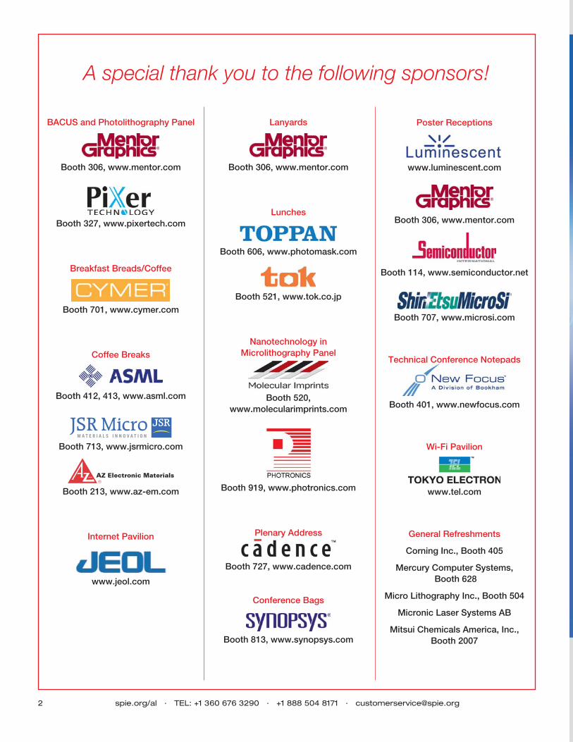
A special thank you to the following sponsors!
BACUS and Photolithography Panel
Booth 306, www.mentor.com
Booth 327, www.pixertech.com
Breakfast Breads/Coffee
Booth 701, www.cymer.com
Coffee Breaks
Booth 412, 413, www.asml.com
Booth 713, www.jsrmicro.com
Booth 213, www.az-em.com
Internet Pavilion
www.jeol.com
Lanyards
Booth 306, www.mentor.com
Lunches
Booth 606, www.photomask.com
Booth 521, www.tok.co.jp
Nanotechnology in Microlithography Panel
Booth 520, www.molecularimprints.com
Booth 919, www.photronics.com
Plenary Address
Booth 727, www.cadence.com
Conference Bags
Booth 813, www.synopsys.com
Poster Receptions
www.luminescent.com
Booth 306, www.mentor.com
Booth 114, www.semiconductor.net
Booth 707, www.microsi.com
Technical Conference Notepads
Booth 401, www.newfocus.com
Wi-Fi Pavilion
www.tel.com
General Refreshments
Corning Inc., Booth 405
Mercury Computer Systems, Booth 628
Micro Lithography Inc., Booth 504
Micronic Laser Systems AB
Mitsui Chemicals America, Inc., Booth 2007
spie.org/al · TEL: +1 360 676 3290 · +1 888 504 8171 · [email protected] 3
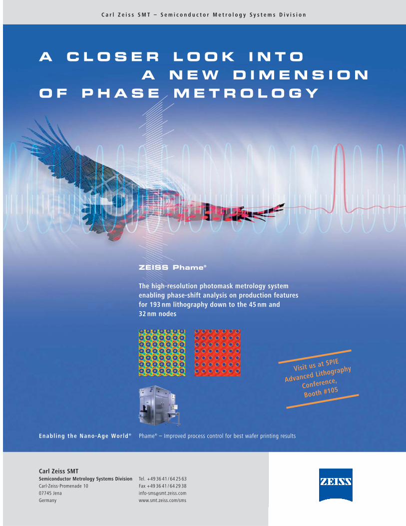
C a r l Z e i s s S M T – S e m i c o n d u c t o r M e t r o l o g y S y s t e m s D i v i s i o n
A C L O S E R L O O K I N T OA N E W D I M E N S I O N
O F P H A S E M E T R O L O G Y
Carl Zeiss SMTSemiconductor Metrology Systems DivisionCarl-Zeiss-Promenade 1007745 JenaGermany
Tel. +49 36 41 / 64 25 63Fax +49 36 41 / 64 29 [email protected]/sms
ZEISS Phame®
The high-resolution photomask metrology system enabling phase-shift analysis on production features for 193 nm lithography down to the 45 nm and 32 nm nodes
Phame® – Improved process control for best wafer printing resultsEnabl ing the Nano-Age World ®
Visit us at SPIE
Advanced Lithography
Conference,
Booth #105
4 spie.org/al · TEL: +1 360 676 3290 · +1 888 504 8171 · [email protected]
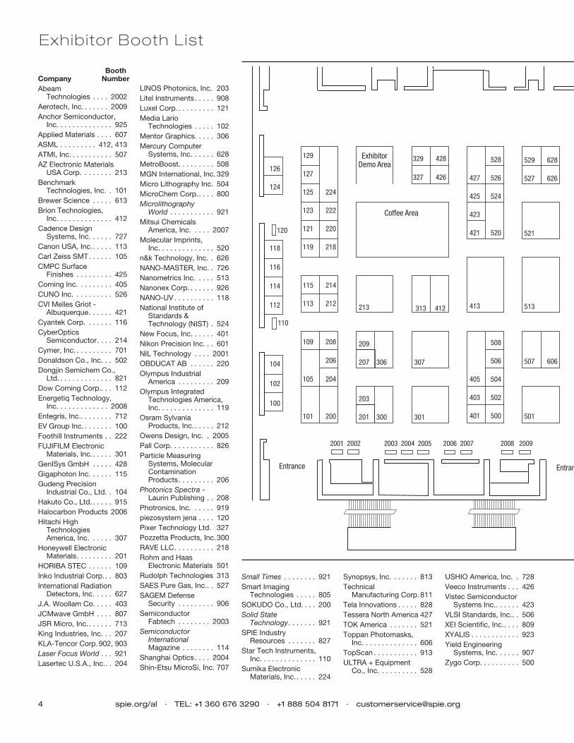
Exhibi tor Booth L ist
LINOS Photonics, Inc. 203Litel Instruments. . . . . 908Luxel Corp. . . . . . . . . . 121Media Lario
Technologies . . . . . 102Mentor Graphics. . . . . 306Mercury Computer
Systems, Inc. . . . . . 628MetroBoost. . . . . . . . . 508MGN International, Inc. 329Micro Lithography Inc. 504MicroChem Corp.. . . . 800Microlithography
World . . . . . . . . . . . 921Mitsui Chemicals
America, Inc. . . . . 2007Molecular Imprints,
Inc. . . . . . . . . . . . . . 520n&k Technology, Inc. . 626NANO-MASTER, Inc. . 726Nanometrics Inc. . . . . 513Nanonex Corp. . . . . . . 926NANO-UV . . . . . . . . . . 118National Institute of
Standards & Technology (NIST) . 524
New Focus, Inc. . . . . . 401Nikon Precision Inc. . . 601NIL Technology . . . . 2001OBDUCAT AB . . . . . . 220Olympus Industrial
America . . . . . . . . . 209Olympus Integrated
Technologies America, Inc. . . . . . . . . . . . . . 119
Osram Sylvania Products, Inc. . . . . . 212
Owens Design, Inc. . 2005Pall Corp. . . . . . . . . . . 826Particle Measuring
Systems, Molecular Contamination Products. . . . . . . . . 206
Photonics Spectra - Laurin Publishing . . 208
Photronics, Inc. . . . . . 919piezosystem jena . . . . 120Pixer Technology Ltd. 327Pozzetta Products, Inc. 300RAVE LLC. . . . . . . . . . 218Rohm and Haas
Electronic Materials 501Rudolph Technologies 313SAES Pure Gas, Inc.. . 527SAGEM Defense
Security . . . . . . . . . 906Semiconductor
Fabtech . . . . . . . . 2003Semiconductor
International Magazine . . . . . . . . 114
Shanghai Optics . . . . 2004Shin-Etsu MicroSi, Inc. 707
Small Times . . . . . . . . 921Smart Imaging
Technologies . . . . . 805SOKUDO Co., Ltd. . . . 200Solid State
Technology. . . . . . . 921SPIE Industry
Resources . . . . . . . 827Star Tech Instruments,
Inc. . . . . . . . . . . . . . 110Sumika Electronic
Materials, Inc.. . . . . 224
Booth Company NumberAbeam
Technologies . . . . 2002Aerotech, Inc. . . . . . . 2009Anchor Semiconductor,
Inc. . . . . . . . . . . . . . 925Applied Materials . . . . 607ASML . . . . . . . . . 412, 413ATMI, Inc. . . . . . . . . . . 507AZ Electronic Materials
USA Corp. . . . . . . . 213Benchmark
Technologies, Inc. . 101Brewer Science . . . . . 613Brion Technologies,
Inc. . . . . . . . . . . . . . 412Cadence Design
Systems, Inc. . . . . . 727Canon USA, Inc.. . . . . 113Carl Zeiss SMT. . . . . . 105CMPC Surface
Finishes . . . . . . . . . 425Corning Inc. . . . . . . . . 405CUNO Inc. . . . . . . . . . 526CVI Melles Griot -
Albuquerque. . . . . . 421Cyantek Corp. . . . . . . 116CyberOptics
Semiconductor. . . . 214Cymer, Inc. . . . . . . . . . 701Donaldson Co., Inc. . . 502Dongjin Semichem Co.,
Ltd. . . . . . . . . . . . . . 821Dow Corning Corp.. . . 112 Energetiq Technology,
Inc. . . . . . . . . . . . . 2008Entegris, Inc.. . . . . . . . 712EV Group Inc. . . . . . . . 100Foothill Instruments . . 222FUJIFILM Electronic
Materials, Inc.. . . . . 301GenISys GmbH . . . . . 428Gigaphoton Inc. . . . . . 115Gudeng Precision
Industrial Co., Ltd. . 104Hakuto Co., Ltd. . . . . . 915Halocarbon Products 2006Hitachi High
Technologies America, Inc. . . . . . 307
Honeywell Electronic Materials. . . . . . . . . 201
HORIBA STEC . . . . . . 109Inko Industrial Corp. . . 803International Radiation
Detectors, Inc. . . . . 627J.A. Woollam Co. . . . . 403JCMwave GmbH . . . . 807JSR Micro, Inc.. . . . . . 713King Industries, Inc. . . 207KLA-Tencor Corp. 902, 903Laser Focus World . . . 921Lasertec U.S.A., Inc.. . 204
Synopsys, Inc. . . . . . . 813Technical
Manufacturing Corp. 811Tela Innovations . . . . . 828Tessera North America 427TOK America . . . . . . . 521Toppan Photomasks,
Inc. . . . . . . . . . . . . . 606TopScan . . . . . . . . . . . 913ULTRA + Equipment
Co., Inc. . . . . . . . . . 528
126
124
118
116
114
112
104
102
100
129
127
125 224
123 222
121 220
119 218
115 214
113 212
109 208
206
105 204
101 200
329 428
327 426
Coffee Area
ExhibitorDemo Area
EntranEntrance
313 412
307
301
213
209
207 306
203
201 300
528
427 526
425 524
423
421 520
413
508
506
405 504
403 502
401 500
529 628
527 626
521
513
507 606
501
2001 2002 2003 2004 2005 2006 2007 2008 2009
120
110
USHIO America, Inc. . 728Veeco Instruments . . . 426Vistec Semiconductor
Systems Inc.. . . . . . 423VLSI Standards, Inc.. . 506XEI Scientifi c, Inc.. . . . 809XYALIS . . . . . . . . . . . . 923Yield Engineering
Systems, Inc. . . . . . 907Zygo Corp. . . . . . . . . . 500
spie.org/al · TEL: +1 360 676 3290 · +1 888 504 8171 · [email protected] 5
Coffee Area
Lunch and Seating Area
rance
Entrance
Entrance to Registration
Registration Area
Lunch and Seating Area
613 712
607
601
713
707
701 800
629 728
627 726
828
727 826
928
827 926
821
813
908
906
902
929
927
925
923
921
919
915
913
907
903
Entrance toRegistration
811
809
807
805
803
Exhibitor Service Area
Exhibitor Lounge
Convent ion Center Exhib i t ion F loor
Advertisers IndexCarl Zeiss SMT . . . . . . . . . . . . . . . . . . . . . . . . . . . . . 3
Mentor Graphics Corp. . . . . . . . . . inside front cover
Nano-Master, Inc.. . . . . . . . . . . . . . . . . . . . . . . . . . 10
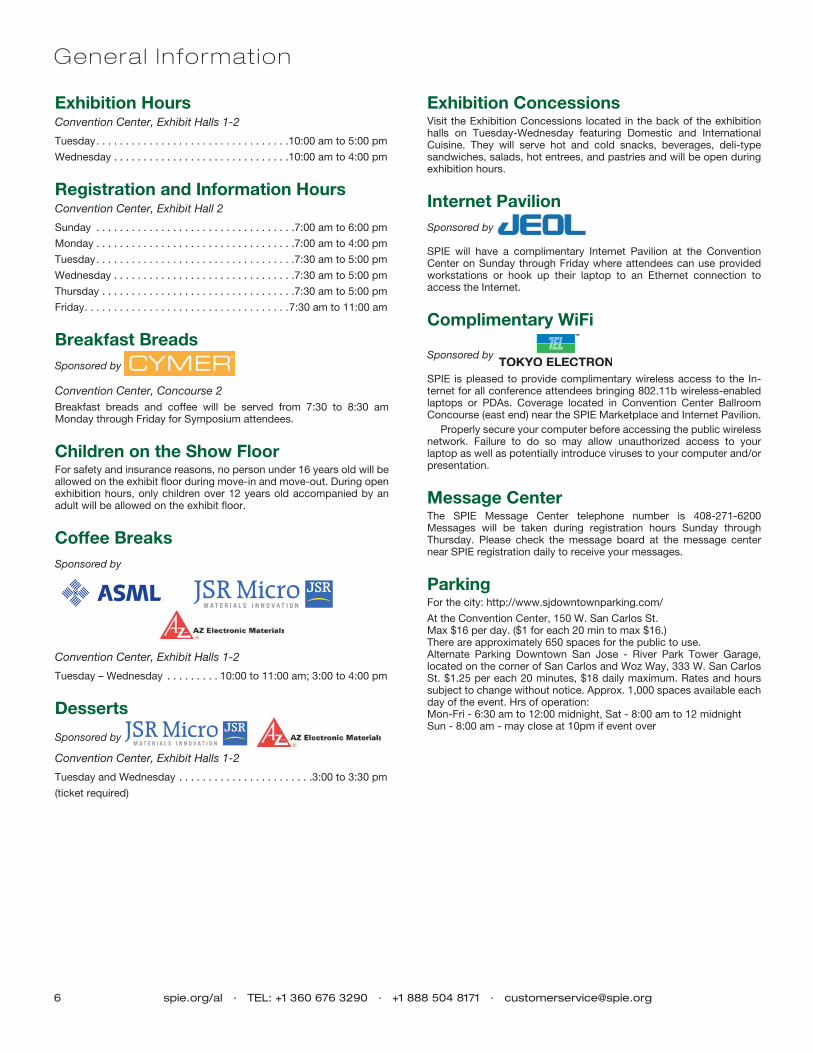
6 spie.org/al · TEL: +1 360 676 3290 · +1 888 504 8171 · [email protected]
Exhibition HoursConvention Center, Exhibit Halls 1-2
Tuesday . . . . . . . . . . . . . . . . . . . . . . . . . . . . . . . . .10:00 am to 5:00 pm
Wednesday . . . . . . . . . . . . . . . . . . . . . . . . . . . . . .10:00 am to 4:00 pm
Registration and Information HoursConvention Center, Exhibit Hall 2
Sunday . . . . . . . . . . . . . . . . . . . . . . . . . . . . . . . . . .7:00 am to 6:00 pm
Monday . . . . . . . . . . . . . . . . . . . . . . . . . . . . . . . . . .7:00 am to 4:00 pm
Tuesday . . . . . . . . . . . . . . . . . . . . . . . . . . . . . . . . . .7:30 am to 5:00 pm
Wednesday . . . . . . . . . . . . . . . . . . . . . . . . . . . . . . .7:30 am to 5:00 pm
Thursday . . . . . . . . . . . . . . . . . . . . . . . . . . . . . . . . .7:30 am to 5:00 pm
Friday . . . . . . . . . . . . . . . . . . . . . . . . . . . . . . . . . . .7:30 am to 11:00 am
Breakfast BreadsSponsored by
Convention Center, Concourse 2Breakfast breads and coffee will be served from 7:30 to 8:30 am Monday through Friday for Symposium attendees.
Children on the Show FloorFor safety and insurance reasons, no person under 16 years old will be allowed on the exhibit fl oor during move-in and move-out. During open exhibition hours, only children over 12 years old accompanied by an adult will be allowed on the exhibit fl oor.
Coffee BreaksSponsored by
Convention Center, Exhibit Halls 1-2
Tuesday – Wednesday . . . . . . . . . 10:00 to 11:00 am; 3:00 to 4:00 pm
Desserts
Sponsored by
Convention Center, Exhibit Halls 1-2
Tuesday and Wednesday . . . . . . . . . . . . . . . . . . . . . . .3:00 to 3:30 pm
(ticket required)
General Informat ion
Exhibition ConcessionsVisit the Exhibition Concessions located in the back of the exhibition halls on Tuesday-Wednesday featuring Domestic and International Cuisine. They will serve hot and cold snacks, beverages, deli-type sandwiches, salads, hot entrees, and pastries and will be open during exhibition hours.
Internet PavilionSponsored by
SPIE will have a complimentary Internet Pavilion at the Convention Center on Sunday through Friday where attendees can use provided workstations or hook up their laptop to an Ethernet connection to access the Internet.
Complimentary WiFi
Sponsored by
SPIE is pleased to provide complimentary wireless access to the In-ternet for all conference attendees bringing 802.11b wireless-enabled laptops or PDAs. Coverage located in Convention Center Ballroom Concourse (east end) near the SPIE Marketplace and Internet Pavilion. Properly secure your computer before accessing the public wireless network. Failure to do so may allow unauthorized access to your laptop as well as potentially introduce viruses to your computer and/or presentation.
Message Center The SPIE Message Center telephone number is 408-271-6200 Messages will be taken during registration hours Sunday through Thursday. Please check the message board at the message center near SPIE registration daily to receive your messages.
ParkingFor the city: http://www.sjdowntownparking.com/
At the Convention Center, 150 W. San Carlos St.Max $16 per day. ($1 for each 20 min to max $16.)There are approximately 650 spaces for the public to use.Alternate Parking Downtown San Jose - River Park Tower Garage, located on the corner of San Carlos and Woz Way, 333 W. San Carlos St. $1.25 per each 20 minutes, $18 daily maximum. Rates and hours subject to change without notice. Approx. 1,000 spaces available each day of the event. Hrs of operation:Mon-Fri - 6:30 am to 12:00 midnight, Sat - 8:00 am to 12 midnightSun - 8:00 am - may close at 10pm if event over
spie.org/al · TEL: +1 360 676 3290 · +1 888 504 8171 · [email protected] 7
Tuesday
10:30 am
Custom Fabrication of Components for Semiconductor Tooling William Ackerman, CMPC Surface Finishes
Achieving nanoscale tolerances and superior surface properties over large areas on a broad array of hard ceramics, metals, and glasses used in semiconductor and lithography tooling.
11:30 am
Laser-Driven Light Source. High-Brightness from DUV to Vis Paul Blackborow, Energetiq Technology, Inc.
Brighter than the brightest arc-lamps and deuterium lamps, The Laser-Driven Light Source™ provides broadband spectral output or is fi ltered for 193nm, 248nm, 365nm or any band from DUV to vis.
12:30 pm
Improving Time to Volume Manufacturing by Design Including Double Patterning Bob Naber, Cadence Design Systems, Inc.
As consumer products increasingly drive the semiconductor industry, time to volume manufacturing is critical in the success of a product. Witness the benefi ts of preventing, analyzing, and optimizing manufacturability variations in the design space to ensure that your design is correct by construction. Find out about a more streamlined fl ow to implement double patterning techniques.
1:30 pm
MX 61A Automated Failure Analysis Microscope Matt Smith, Olympus Industrial America
Fully automated microscope systems. Includes full three-axis control for wafers up to 300 mm in diameter along with the integration of digital imaging with complete image analysis capabilities.
2:30 pm
Parallel Processing of the Manufacturing Flow George E. Bailey, Synopsys
Witness Synopsys’ latest parallel processing capability (Proteus++). This new concept will revolutionize the manufacturing fl ow by enabling parallel processing of OPC, LRC, MDP and MRC. This solution reduces the I/O bottleneck, eliminates memory spikes, maximizes CPU utilization, and provides unmatched TAT with general purpose hardware.
Product Demonstrat ions
Photography/Video PolicyIn the Exhibition Hall: For security and courtesy reasons, photographing or videotaping individual booths and displays in the exhibit hall is allowed ONLY with explicit permission from on-site company representatives. Individuals not complying with this policy will be asked to surrender their fi lm and to leave the exhibition hall.
Quicklunch Coupons
Tuesday lunch sponsored by
Wednesday lunch sponsored by
Full conference registrants will receive a lunch coupon redeemable towards a luncheon purchased Tuesday and Wednesday at designated areas of the Exhibit Hall. Coupons will be accepted from 11:30am to 1:30 pm both days. Some restrictions apply; please refer to the coupons in your registration packet.
SPIE Copy CenterSunday through Thursday during registration hours San Diego Copy will provide a copy service during the week for symposium attendees. The rates are 5 cents per copy. The Copy Center will be located near registration.
SPIE MarketplaceOpen during Registration hours
The SPIE Marketplace is your source for the latest SPIE Press books, Proceedings, and Educational and Professional Development materials. Become a Member of SPIE, explore the Digital Library, and take home a souvenir.
No Unauthorized SolicitationPlease note that while all meeting attendees are invited to the exhibition, any attendee who is observed to be soliciting business in the aisles or other public spaces, in another company’s booth, or in violation of any portion of the SPIE Exhibition Policy, will be asked to leave immediately. Additional penalties may be applied. Please report any violations you may observe to show management.

8 spie.org/al · TEL: +1 360 676 3290 · +1 888 504 8171 · [email protected]
Sunday Monday Tuesday Wednesday Thursday
SC101 Introduction to Microlithography: Theory, Materials, and Processing (Bowden, Thompson, Willson) 8:30 am to 5:30 pm, $595 / $695
SC103 Chemically Amplifi ed Resists (Willson) 8:30 am to 5:30 pm, $530 / $630
SC616 Practical Photoresist Processing (Dammel) 1:30 to 5:30 pm, $315 / $365
Design for Manufacturability through Design-Process IntegrationSC540 Applying Optical Proximity Correction and Design for Manufacturability to Product Designs (Capodieci, Lucas) 8:30 am to 5:30 pm, $530 / $630
SC105 CD Metrology and Image Formation in the Scanning Electron Microscope (SEM) (Wells, Postek) 8:30 am to 5:30 pm, $580 / $680
SC116 Lithographic Optimization: A Theoretical Approach (Mack) 8:30 am to 5:30 pm, $570 / 670
SC833 Lithography Integration for Semiconductor Back-End-Of-The-Line (BEOL) (Lin) 8:30 am to 12:30 pm, $315 / $365
NEW SC885 Principles and Practical Implementation of Double Patterning (Dusa) 8:30 am to 12:30 pm, $315 / $365
NEW SC887 Modeling of Exposure Tools (Lai) 1:30 to 5:30 pm, $315 / $365
NEW SC855 Introduction to Design for Manufacturability (Liebmann, Wong) 1:30 to 5:30 pm, $315 / $365
NEW SC889 Layout-Aware Circuit Analysis (Singh, Heng, Bansal) 8:30 am to 12:30 pm, $315 / $365
NEW SC856 Computational Lithography (Mansfi eld, Wong) 1:30 to 5:30 pm, $315 / $365
Emerging Lithographic TechnologiesNEW SC890 Electron-Beam Lithography - Current Use and Recent Advances (Pfeiffer, McCord) 8:30 am to 5:30 pm, $530 / $630
SC888 EUV Lithography (Bakshi, Soufl i, Ahn, Naulleau) 8:30 am to 6:30 pm, $740 / $840
SC101 Introduction to Microlithography: Theory, Materials, and Processing (Bowden, Thompson, Willson) 8:30 am to 5:30 pm, $595 / $695
SC622 Nano-Scale Patterning with Imprint Lithography (Sreenivasan, Willson, Resnick) 6:00 to 10:00 pm, $315 / $365
Intellectual Property & PatentsWS619 Intellectual Assets for Micro/Nano Electronics and Lithography (Cole) 1:30 to 5:30 pm, $315 / $365
Dai ly Course Schedule
Advances in Resist Materials and Processing Technology
Register for courses onsite at the SPIE Cashier!
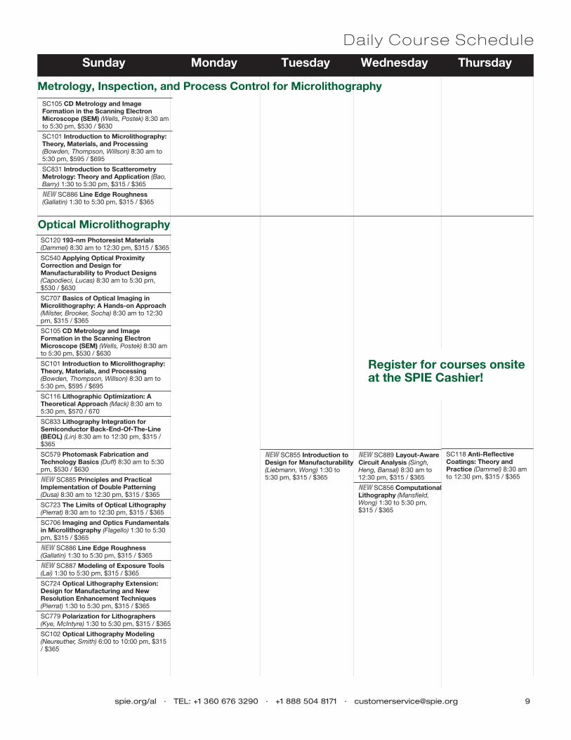
spie.org/al · TEL: +1 360 676 3290 · +1 888 504 8171 · [email protected] 9
Sunday Monday Tuesday Wednesday Thursday
Metrology, Inspection, and Process Control for MicrolithographySC105 CD Metrology and Image Formation in the Scanning Electron Microscope (SEM) (Wells, Postek) 8:30 am to 5:30 pm, $530 / $630
SC101 Introduction to Microlithography: Theory, Materials, and Processing (Bowden, Thompson, Willson) 8:30 am to 5:30 pm, $595 / $695
SC831 Introduction to Scatterometry Metrology: Theory and Application (Bao, Barry) 1:30 to 5:30 pm, $315 / $365
NEW SC886 Line Edge Roughness (Gallatin) 1:30 to 5:30 pm, $315 / $365
NEW SC855 Introduction to Design for Manufacturability (Liebmann, Wong) 1:30 to 5:30 pm, $315 / $365
NEW SC889 Layout-Aware Circuit Analysis (Singh, Heng, Bansal) 8:30 am to 12:30 pm, $315 / $365
NEW SC856 Computational Lithography (Mansfi eld, Wong) 1:30 to 5:30 pm, $315 / $365
SC118 Anti-Refl ective Coatings: Theory and Practice (Dammel) 8:30 am to 12:30 pm, $315 / $365
Optical MicrolithographySC120 193-nm Photoresist Materials (Dammel) 8:30 am to 12:30 pm, $315 / $365
SC540 Applying Optical Proximity Correction and Design for Manufacturability to Product Designs (Capodieci, Lucas) 8:30 am to 5:30 pm, $530 / $630
SC707 Basics of Optical Imaging in Microlithography: A Hands-on Approach (Milster, Brooker, Socha) 8:30 am to 12:30 pm, $315 / $365
SC105 CD Metrology and Image Formation in the Scanning Electron Microscope (SEM) (Wells, Postek) 8:30 am to 5:30 pm, $530 / $630
SC101 Introduction to Microlithography: Theory, Materials, and Processing (Bowden, Thompson, Willson) 8:30 am to 5:30 pm, $595 / $695
SC116 Lithographic Optimization: A Theoretical Approach (Mack) 8:30 am to 5:30 pm, $570 / 670
SC833 Lithography Integration for Semiconductor Back-End-Of-The-Line (BEOL) (Lin) 8:30 am to 12:30 pm, $315 / $365
SC579 Photomask Fabrication and Technology Basics (Duff) 8:30 am to 5:30 pm, $530 / $630
NEW SC885 Principles and Practical Implementation of Double Patterning (Dusa) 8:30 am to 12:30 pm, $315 / $365
SC723 The Limits of Optical Lithography (Pierrat) 8:30 am to 12:30 pm, $315 / $365
SC706 Imaging and Optics Fundamentals in Microlithography (Flagello) 1:30 to 5:30 pm, $315 / $365
NEW SC886 Line Edge Roughness (Gallatin) 1:30 to 5:30 pm, $315 / $365
NEW SC887 Modeling of Exposure Tools (Lai) 1:30 to 5:30 pm, $315 / $365
SC724 Optical Lithography Extension: Design for Manufacturing and New Resolution Enhancement Techniques (Pierrat) 1:30 to 5:30 pm, $315 / $365
SC779 Polarization for Lithographers (Kye, McIntyre) 1:30 to 5:30 pm, $315 / $365
SC102 Optical Lithography Modeling (Neureuther, Smith) 6:00 to 10:00 pm, $315 / $365
Dai ly Course Schedule
Register for courses onsite at the SPIE Cashier!
spie.org/al · TEL: +1 360 676 3290 · +1 888 504 8171 · [email protected] 11
Abeam Technologies #20025286 Dunnigan Ct, Castro Valley, CA, 94546510/538-4862www.abeamtech.com
New Product: CHARIOT: CD-SEM simulation and calibration; BEAMETR: automatic beam size measurement; NTegra: AFM.
Abeam Technologies Inc. develops calibration tools for e-beam systems and modeling software used in microelectronic industry to optimize fabrication processes. The company has its headquarters in California, representative companies in Japan, Europe and Korea and a group of software developers and mathematicians in Russia. Contact: Sergey Babin, [email protected].
Aerotech, Inc. #2009
101 Zeta Dr, Pittsburgh, PA, 15238-2897412/963-7470; fax 412/[email protected]; www.aerotech.com
New Product: ABL1500 Series Linear Air-Bearing Stage for High-Performance Scanning and Inspection Applications.
Aerotech manufactures a variety of products, from motors, drives and controllers to fully integrated mechanical and air-bearing stage systems. Our systems and components are used in applications including lithography, high-precision wafer processing, fl at-panel display fabrication and laser micromachining. Aerotech also specializes in vacuum applications like reticle manufacturing, direct-write systems and wafer inspection. Contact: John Lindell, Product Manager, Positioning Systems Division, [email protected].
Anchor Semiconductor Inc. #925
5403 Betsy Ross Dr, Santa Clara, CA, 95054408/986-8969; fax 408/986-8999www.anchorsemi.com
METER BOARD SPONSOR
Applied Materials #6073050 Bowers Ave, Santa Clara , CA, 95050408/727-5555www.amat.comApplied Materials, Inc. is the global leader in Nanomanufacturing Technology™ solutions for the electronics industry with a broad portfolio of innovative equipment, service and software products. At Applied Materials, we apply nanomanufacturing technology to improve the way people live.
COFFEE BREAK SPONSOR
ASML #412, 413
8555 S River Pky, Tempe, AZ, 85284480/383-4422; fax 480/[email protected]; www.asml.comASML is the world’s leading provider of lithography systems for the semiconductor industry. We are committed to providing customers with the right technology that is production-ready at the right time. The TWINSCAN lithography platform and our advancements with our immersion lithography systems show our technology leadership and enable our customers and their customers to sustain their competitive edge. ASML operates sales and service in over 60 locations in 14 countries.
ATMI, Inc. #50710851 Louisiana Ave S, Minneapolis, MN, 55438952/942-0855; fax 952/942-8474www.atmi.com
New Product: NOWTrak™ Network - a consumable material management system brings control to critical manufacturing.
ATMI delivers smart and active materials-delivery solutions. Our NOWPak® product line offers liner-based containment and dispensing systems to maintain the purity and cleanliness of critical chemicals. The chemical key-coding of the closures and connectors ensures chemical misconnect prevention, while NOWTrak™ Network a consumable material management system brings control to critical manufacturing. Our solutions enhance process yields and reduced costs. Contact: Rick Wilson, Sales, [email protected]; Brad Williams, Sales, [email protected].
COFFEE BREAK SPONSOR
AZ Electronic Materials USA Corp. #21370 Meister Ave, Branchburg, NJ, 08876-3440908/429-3538; fax 908/429-3631www.az-em.comAZ Electronic Materials is an independent specialty chemicals business with plants in Taiwan, Korea, China, Japan, France, Germany and the United States and provides anti-relective coatings, other specialty coatings and photoresists for the integrated circuits and devices industries. Contact: Kathryn Durham, Director, Marketing, Quality and Sales Support. [email protected]
Benchmark Technologies, Inc. #1017E Kimball Ln, Lynnfi eld, MA, 01940781/246-3303; fax 781/[email protected]; www.benchmarktech.com
New Product: Nano-Imprint Test Template
Benchmark Technologies is the premier provider of test reticles for all aspects of lithography tool monitoring and characterization, including: monitoring of focus, polarization, resolution and defects, and matching of overlay from tool to tool. Reticles for double patterning process development are also available. The company also offers turnkey services to supply CAD and fabrication of photomasks, relief structure masters and replicas for nano-imprint, and patterned test wafers.
Brewer Science #613
2401 Brewer Dr, Rolla, MO, 65401573/364-0300; fax 573/364-6880www.brewerscience.com
New Product: Providing 193 ARC® Solutions for low defectivity, immersion, fast etch and high Na applications.
Brewer Science is a leading-edge material supplier to the semiconductor, advanced packaging, MEMS, nanotechnology, optoelectronic and compound semiconductor industries. Product lines include ARC® (Anti-Refl ective Coating) spin-on coatings for microlithography applications, carbon nanotube solutions and materials that enable thin wafer handling, TSV formation, wafer thinning, wafer etching and bulk micromachining. Contact: Rick Miller, Global Sales Manager, [email protected].
Exhibi tor Directory
12 spie.org/al · TEL: +1 360 676 3290 · +1 888 504 8171 · [email protected]
Brion Technologies, Inc. #412
4211 Burton Dr, Santa Clara, CA, 95054408/653-1500; fax 408/[email protected]; www.briontech.comBrion, an ASML company, is the pioneer and worldwide leader in computational lithography for integrated circuits. Brion leads the global market for optical proximity correction (OPC) verifi cation and is rapidly expanding in the OPC market with Tachyon OPC+. Brion’s Tachyon products deliver both speed and accuracy for advanced process nodes. By combining image-based computing and hardware-accelerated co-processing, Brion enables exceptional design and verifi cation accuracy without compromising the speed or productivity of the circuit manufacturing process.
PLENARY SPONSOR
Cadence Design Systems, Inc. #7272655 Seely Ave, San Jose, CA, 95134408/943-1234www.cadence.com
New Product: DFM, RET, OPC products to improve time to volume production in the pre and post GDS tapeout fl ow.
Cadence enables global electronic-design innovation and plays an essential role in the creation of today’s integrated circuits and electronics. Customers use Cadence software and hardware, methodologies and services to design and verify advanced semiconductors, consumer electronics, networking and telecommunications equipment and computer systems. Contact: Bob Naber, Product Marketing Director, [email protected].
Canon USA, Inc. #113
3300 N First St, San Jose, CA, 95134408/468-2000; fax 408/[email protected] ; www.usa.canon.comCanon supplies step-and-repeat and step-and-scan photolithography tools for high volume manufacturing of a wide range of leading edge semiconductor device, read/write heads for magnetic storage systems and microelectromechanical systems (MEMS).
Carl Zeiss SMT #105
One Corporation Way, Peabody, MA, 01960978/826-1500; fax 978/[email protected]; www.smt.zeiss.com
New Product: The high-resolution metrology system Phame allows for in-die phase-shift measurement on all PSMs.
The Semiconductor Metrology Systems Division of Carl Zeiss SMT is a leading supplier of metrology and manufacturing equipment for the semiconductor industry. Core expertise in light and electron optics is the foundation for a product portfolio spanning from photomask metrology and photomask repair to structural modifi cation of semiconductor substrates. The AIMS™, MeRiT® and Phame® product families provide our customers with a comprehensive solution for photomask defect verifi cation and repair. Contact: Jim Polcyn, United States Sales Director, [email protected].
CMPC Surface Finishes #42539 Offi cial Rd, Addison, IL, 60101630/543-6682; fax 630/543-4013sales@ensurfi n.com;
New Product: Low scatter aluminum mirrors.
Since 1949, Surface Finishes has been a leader in precision lapping, grinding and optical polishing techniques specializing in fl at, cylindrical, perpendicular and parallel surfaces with extremely demanding geometry. These capabilities produce Angstrom level tolerances on components such as: mirrors for optical imaging and scanning, air bearings, vacuum chucks, optical disc molds, large area reference surfaces and custom gauging. Free engineering advice for your most challenging applications. Contact: David Patterson, Account Manager, [email protected]; Daniel McMullen, Director, Business Development, [email protected].
GENERAL REFRESHMENT SPONSOR
Corning Inc. #405
1 Riverfront Plaza, Corning, NY, 14831607/974-9000www.corning.comCorning Incorporated is a premier supplier of advanced optical solutions for the world’s leading semiconductor equipment manufacturers. World-class materials manufacturing, a long heritage in optical design and manufacturing and state of the art metrology enable Corning to keep pace with the toughest optical requirements of today and the next generation. Contact: Dave Young, Marketing Communications, [email protected]; Elijah Baity, Market Analyst, [email protected].
CUNO Inc. #526400 Research Pkwy, Meriden, CT, 06450203/237-5541; fax 203/630-4530www.cuno.comCUNO fi lter systems deliver premium performance for process water treatment, electronics chemical and photoresist production and CMP slurry distribution. Utilizing a patented charge modifi cation technology, CUNO’s membrane fi lters remain the most effective deterrent to contamination in water applications. PTFE membrane and stainless steel media for chemical and gas fi ltration and 316L stainless steel housings complete a comprehensive range of products for the semiconductor industry. Contact: Bob Gieger, Market Manager, Electronics, [email protected].
CVI Melles Griot - Albuquerque #421
200 Dorado Pl SE, Albuquerque, NM, 87123800/296-9541; fax 505/298-9908www.cvimellesgriot.comCVI Melles Griot gets you what you need, when you need it. From the UV to the IR we offer unmatched breadth and fl exibility in lasers, optical components, and electro-optical assemblies. Our extensive catalog, along with our custom and build-to-print capabilities deliver solutions from prototype to high-volume, OEM quantities. Providing solutions for semiconductor, biotechnology, industrial, and basic research applications, CVI Melles Griot manufactures on three continents, and maintains sales and engineering centers in 11 countries worldwide. Contact: Rich Drake, Sales Manager, West Coast, [email protected]
Exhibi tor Directory
spie.org/al · TEL: +1 360 676 3290 · +1 888 504 8171 · [email protected] 13
Cyantek Corp. #116
3055 Osgood Ct, Fremont, CA, 94539510/651-3341; fax 510/[email protected]; www.cyantek.comWhether your needs are for specialty etchants, positive resist developers, organic strippers or mask cleaners, Cyantek has a broad range of products that can meet you requirements. We also offer customized blends to help you address your most demanding process needs. Our products are utilized in photo mask, IC, thin fi lm, FPD, nanotechnology and PV manufacturing technologies. Call us or visit our website for more information. Contact: Dale Deg, Sales and Marketing Manager, [email protected].
CyberOptics Semiconductor #21413555 SW Millikan Way, Beaverton, OR, 97035503/495-2200; fax 503/[email protected]; www.cyberopticssemi.com
New Product: WaferSense® AVS wirelessly monitors vibrations that may impact photolithography process yields.
Innovating measurement technology: EX-Q / EX-QS wafer mapper sensors. WaferSense® ALS Auto Leveling System for level, co-planarity and inclination; WaferSense ATS Auto Teaching System for robot handoff maintenance; WaferSense AGS Auto Gapping System for PE-CVD and Etch setup; WaferSense AVS Auto Vibration System for wafer acceleration and Automatic Material Handling Systems AMHS FOUP optimization. Contact: Craig Ramsey, General Manager, [email protected]; Mark Hannaford, Sales Manager, [email protected].
HOTEL KEYS • METER BOARD • BREAKFAST SPONSOR
Cymer, Inc. #70117075 Thornmint Ct, San Diego, CA, 92127858/385-7300; fax 858/385-6601www.cymer.comCymer, Inc. is the world’s leading supplier of deep ultraviolet (DUV) laser illumination sources, the essential light source for DUV photolithography systems. DUV lithography is a key enabling technology, which has allowed the semiconductor industry to meet the exacting specifi cations and manufacturing requirements for volume production of today’s advanced semiconductor chips.
Donaldson Co., Inc. #502PO Box 1299, Minneapolis, MN, 55440952/887-3325; fax 952/887-3612www.donaldson.com
New Product: ChemCore fi lters, awarded Controlled Environments Magazine 2007 Experts’ Choice Award.
Donaldson provides Semiconductor manufacturers with fi ltration solutions that increase product yields and uptime. We focus on the comprehensive elimination of gas-phase and particulate airborne molecular contamination at the zone, tool, and point-of-use levels. Contact: Kent Hemminger, Semiconductor Sales Manager, [email protected]; Dan Lynch, Semiconductor Salesperson, [email protected].
Dongjin Semichem Co., Ltd. #821
625-3 Yodang-ri, Yanggam-Myun, Hwasung-kun, Kyungki-si, South Korea, 445-93082 31 350 5557; fax 82 31 353 6459www.dongjin.comDONGJIN SEMICHEM CO., LTD. offers photoresists, bottom ARC, CMP slurries, colored resists, column spacer, organic insulator designed to meet the requirements of the semiconductor and the fl at-panel display industry. Our product line includes thinner, stripper, developer, rinsing solution and etchants. Contact: Jaehyun Kim, Executive director, [email protected]; Hyun-Jin Kim, Manager, [email protected].
Dow Corning Corp #112Electronics, 2200 W Salzburg Rd, Midland, MI, 48686989/496-4000; fax 989/[email protected]; www.dowcorning.comDow Corning Silicon Lithography Solutions, a segment of Dow Corning Electronics Solutions business, is your source for silicon photoresists and antirefl ective coatings. We provide customized silicon resins for advanced lithography applications. Our proven capabilities of silicon materials development, commercialization and global supply enable leading lithography material suppliers and integrated circuit manufacturers to innovate and excel. To learn more, go to www.dowcorning.com/lithography. Contact: Jeff Bremmer, Global Marketing Manager, [email protected]; Ken Seibert, Marketing, [email protected].
Energetiq Technology, Inc. #20087 Constitution Way, Woburn, MA, 01801781/939-0763; fax 781/[email protected]; www.energetiq.com
New Product: EQ-1000, Ultra high brightness, broadband DUV-vis 180nm-800nm Laser-Driven Light Source™.
Energetiq is a leader in advanced short-wavelength light sources. Products include the EQ-10 series of EUV and Soft X-ray sources, Saturn 10kW high-power DUV lamps for wafer processing and the new range of ultra high brightness broadband Laser-Driven Light Sources. Contact: Debbie Gustafson, Vice President Sales and Support, [email protected]; Bob Angeli, Global Sales Manager, [email protected].
Entegris, Inc. #7123500 Lyman Blvd, Chaska, MN, 55318952/556-3131; fax 952/[email protected]; www.entegris.comEntegris is a global leader in materials integrity management, purifying, protecting and transporting critical materials used in the semiconductor and other high tech industries. Entegris provides solutions that protect photoresist processes, exposure tool optics and reticles from particle and airborne molecular contamination. These solutions chemically fi lter, purify and condition the environment around critical lithography components, as well as dispense and purify photoresists and coatings. Contact: Customer Service; Rose Larson, Promotions Specialist, North America, [email protected].
Exhibi tor Directory
14 spie.org/al · TEL: +1 360 676 3290 · +1 888 504 8171 · [email protected]
EV Group Inc. #1007700 S River Pkwy, Tempe, AZ, 85284480/727-9600; fax 480/727-9700www.evgroup.comFounded in 1980, EV Group is a global supplier of wafer bonders, aligners, thin wafer-, temporary bonding and debonding-equipment, photoresist coaters, cleaners and inspection systems for semiconductor, MEMS and emerging nanotechnology markets. Headquartered in St. Florian, Austria, EVG has subsidiaries in Tempe, Arizona; Albany, New York; Yokohama and Fukuoka, Japan; and Chung-Li, Taiwan. For more information, visit www.EVGroup.com and our EVG-TShop “Click, Stop - the new way to shop”. Contact: David Owens, Regional Sales Manager, [email protected]; Renae Bellah, Regional Sales, [email protected].
Foothill Instruments #2225011 Jarvis Ave, La Canada, CA, 91011818/[email protected]; www.foothill-instruments.comFoothill Instruments manufactures fi lm and wafer thickness metrology solutions for packaging, MEMS, semiconductor and related markets. Our fi lm thickness tools are capable of measuring dielectrics such as SU-8 of thickness greater than 500 microns and layers on diffi cult Cu substrates. Our wafer thickness products use breakthrough optical technology to enable wafer thickness measurements from 20 - >500 microns. This includes Si, GaAs, SOI and bumped wafers. Contact: Glenn Houser, President.
FUJIFILM Electronic Materials, Inc. #30180 Circuit Dr, North Kingston, RI, 02852401/431-2487; fax 401/432-3799www.fujifi lm-ffem.com
New Product: Email exhibitor to set up meeting at their booth or receive product literature.
Successful semiconductor manufacturers move quickly, demand quality and require leading technology. We offer the broadest line worldwide of photoresists, polyimides, thin fi lm systems and other high purity chemicals and services to technologically demanding semiconductor customers. Contact: FUJIFILM Electronic Materials, Customer Satisfaction, SPIE_Contact@fujifi lm-ffem.com.
GenISys GmbH #428Eschenstr 66, Taufkirchen, Germany, 8202449 89 3309197 60; fax 49 89 3309197 [email protected]; www.genisys-gmbh.com
New Product: Layout BEAMER provides a new, innovative GUI for complex ebeam data preparation and simulation.
Based in Munich, Germany, GenISys GmbH develops, markets and supports fl exible, high-performance software solutions for the highly effi cient processing of large layout data and the optimization of microstructure fabrication processes. Contact: Paul DePesa, Director, [email protected]; Nezih Unal, Vice President, Sales, [email protected].
Gigaphoton Inc. #115Yokokurashinden 400, Oyama Tochigi, Japan, 323-855881 285 28 8410; fax 81 285 28 [email protected]; www.gigaphoton.com
New Product: ArF excimer laser, GT62A provides 90W output and 6kHz repetition rate and spectrum (E95%) <0.35 pm.
Based in Japan, Gigaphoton Inc. is a worldwide supplier of lithographic light sources (248 nm, 193 nm, EUV) for the semiconductor industry. Founded in 2000, Gigaphoton has grown steadily in Asia and became the leading supplier in Japan. In 2005, Gigaphoton entered strategically the United States and European markets where it is now enjoying rapid growth, offering semiconductor Fabs state-of-the-art technology for mass manufacturing coupled with innovative support and cost management solutions. Contact: Kenji Takahisa, Marketing Manager, [email protected]; Olivier Semprez, United States Marketing Director, [email protected].
Gudeng Precision Industrial Co., Ltd. #104
No 428 Bade St, Shulin City, Taipei, Taiwan, 23857886 2 2680 0980; fax 886 2 2680 [email protected]; www.gudeng.com
New Product: Mask Package, Mask Shipping Box, RSP150, Equipment, Peek Cassette, CMP Ring, TFT-LCD Mask Package
Gudeng Precision Industrial Co., Ltd. focus on the fi eld of semiconductor front-end equipment manufacturing in 2000 and has been assisting customers to enhance their product yield and reduce their production cost by providing custom-made products with innovative design concepts. Presently, Gudeng is the world’s leading photomask total solution provider and our product is widely accepted by customers around the world. Contact: Poshin Lee, Technical Manager, [email protected]; Larry Liu, Sales Manager, [email protected].
Hakuto Co., Ltd. #9151-13 Shinjuku 1-Chome, Shinjukuku Tokyo, Japan, 160-891081 3 3225 8910; fax 81 3 3225 8937www.hakuto.co.jp
New Product: Solution for Haze, RSP150, RSP6025: Mask case, PureAID: Chemical absorber, AdIT: Non-outgas info. sheet.
Since its establishment in 1953, Hakuto, as an engineering trading company, is still agilely delivering the latest information and cutting-edge technologies. Hakuto has continuously developed thanks to our customers’ patronage and support. With our belief in the capability of new technologies to energize and enrich our lives and the earth, we will go forward to realize a more enriched society.
Halocarbon Products #2006887 Kinderkamack Rd, River Edge, NJ, 07661201/262-8899; fax 201/[email protected]; www.halocarbon.comHalocarbon Products Corporation has been putting fl uoro-chemicals to work for customers since 1950 in the agriculture and pharmaceutical industries. Halocarbon is one of the world’s leading producers of specialty aliphatic fl uoro-chemicals. Recently, Halocarbon has introduced a new product line for the semiconductor industry. These products include fl uorinated monomers which can be used in the production of photo resist coatings. We can also custom make these materials to meet your needs. Contact: Ron Epstein, Sales Director, [email protected].
Exhibi tor Directory
spie.org/al · TEL: +1 360 676 3290 · +1 888 504 8171 · [email protected] 15
Hitachi High Technologies America, Inc. #3075100 Franklin Dr, Pleasanton, CA, 94588925/218-2800; fax 925/218-2900www.hitachi-hta.comHitachi metrology systems sets the technology pace in process control instrumentation by incorporating Hitachi’s proven electron optics for controlling critical dimensions in next-generation semiconductor devices. The systems provide high resolution imaging and high throughput with easy operation. The systems are fully network compatible, accommodate 200mm or 300mm wafers and are ideal for CD metrology, process development and defect review applications. Product List: CG4000, RS5000, DesignGauge. Contact: Lorena Page, Manager Metrology Products Dept, [email protected].
Honeywell Electronic Materials #2011349 Moffett Park Dr, Sunyvale, CA, 94089408/962-2098www.electronicmaterials.comHoneywell Electronic Materials is a global leader in the supply of critical materials to the semiconductor industry, enabling our customers to develop innovative technologies and overcome manufacturing challenges. Honeywell’s unparalleled expertise and commitment to disciplined quality processes result in the development of superior, cutting-edge technologies that are now being introduced to the fl at panel display, photovoltaic and printable electronics marketplaces. Contact: Lance Chapman, [email protected].
HORIBA STEC #1099701 Dessau Rd Ste 605, Austin, TX, 78754512/836-9560; fax 512/[email protected]; www.horibastec.com
Inko Industrial Corp. #803
695 Vaqueros Ave, Sunnyvale, CA, 94085408/830-1041; fax 408/[email protected]; www.pellicle-inko.comINKO, a U.S. based company, manufactures a complete line of pellicles for applications ranging from ASIC production, high volume memory production. From broadband to I/G line to 248 nm/193nm DUV lithography. We have the right pellicles for your needs. Contact: Joe Mac, Sales and Customer Service; Sherry Chi, Marketing, [email protected].
International Radiation Detectors, Inc. #6272527 W 237th St Unit A, Torrance, CA, 90505-5243310/534-3661; fax 310/[email protected]; www.ird-inc.com
New Product: Vacuum compatible electronics and photodiodes for beamline and space applications.
Manufacturer of UV/VUV/EUV/X-ray photodiode sensors and electronics. Products include photodiodes for high-stability UV/EUV applications and for high-precision absolute X-ray/UV measurements. IRD also has radiometric device characterization facilities spanning in wavelengths from 190nm to 2500nm. Contact: Raj Korde, President, [email protected]; Jacob Sprunck, Device Physicist, [email protected].
J.A. Woollam Co. #403645 M St Ste 102, Lincoln, NE, 68508-2243402/477-7501; fax 402/[email protected]; www.jawoollam.comJ. A. Woollam Company offers a wide range of spectroscopic ellipsometers for nondestructive materials characterization, including thin fi lm thickness (single and multilayer), optical constants, composition, growth/etch rates and more. Instruments available for research and manufacturing metrology covering spectral ranges from vacuum ultra-violet to far infrared. Offering table-top, in-line and in-situ models. Contact: Sales Department.
JCMwave GmbH #807
Haarer Str 14a, Putzbrunn/Munich, Germany, 8564049 89 460 6568; fax 49 89 460 [email protected]; www.jcmwave.com
New Product: Rigoros Simulation Tools for Advanced Lithography.
JCMwave offers software for precise and fast electromagnetic simulations. Application areas include DUV and EUV lithography, optical metrology, surface plasmons, resonance phenomena, meta-materials, photonic crystals and others. In lithography simulation benchmarks with competing methods JCMwave’s products were superior in accuracy and speed by orders of magnitude. JCMwave is a spin-off company from Zuse Institute Berlin, a leading research institute for applied mathematics. Contact: Lin Zschiedrich, Chief Technical Offi cer, [email protected]; Sven Burger, Marketing Director, [email protected].
COFFEE BREAK SPONSOR
JSR Micro, Inc. #713
1280 N Mathilda Ave, Sunnyvale, CA, 94089408/543-8800; fax 408/543-8872www.jsrmicro.comJSR Micro supplies electronic materials to the world’s leading semiconductor manufacturers. The company designs and produces advanced materials including performance photoresists, immersion materials, CMP consumables, low-k dielectrics and packaging materials. With production facilities on three continents and a vast R&D program with fully-equipped technical support centers, JSR creates customized, cost-effective solutions with uncompromising quality to meet the most demanding product roadmaps. Contact: Mark Dennen, Vice President of Sales, [email protected].
King Industries, Inc. #207Science Rd, Norwalk, CT, 06852203/866-5551; fax 203/[email protected]; www.kingindustries.com
New Product: King will feature technical information on its latest line of K-PURE CRR resin modifi ers.
King is a specialty chemical manufacturer established in 1932. It supplies the electronic industry with products for photoresists and back end applications including; thermal acid generators, catalysts, resin modifi ers and corrosion inhibitors. Contact: Dan Miller, Market Development Manager, [email protected]; Michel Hourani, Vice President Commercial Development, [email protected].
Exhibi tor Directory
16 spie.org/al · TEL: +1 360 676 3290 · +1 888 504 8171 · [email protected]
KLA-Tencor Corp. #902, 903
160 Rio Robles, San Jose, CA, 95134408/875-3000; fax 408/[email protected]; www.kla-tencor.comKLA-Tencor Corporation is the world’s leading supplier of inspection, measurement products and solutions used for advanced process control and yield management in the semiconductor, photomask manufacturing and related industries. The company’s comprehensive portfolio of tools, software, analysis, services and expertise is designed to help customers optimize yield throughout the entire process from R&D to fi nal yield analysis in production.
PROMOTIONAL PARTNER
Laser Focus World #92198 Spit Brook Rd, Nashua, NH, 03062603/891-9231; fax 603/891-9290www.laserfocusworld.com
Lasertec U.S.A., Inc. #204
2025 Gateway Pl Ste 480, San Jose, CA, 95110408/437-1441; fax 408/437-1430www.lasertec.co.jpLasertec’s Confocal Laser Scanning Microscopes display high resolution images in real time. The new 410nm laser system allows line width measurements down to 0.15 microns. Non contact surface profi ling with 0.03 microns resolution is possible. Contact: Tom Pomposo, Director of Sales.
LINOS Photonics, Inc. #203
459 Fortune Blvd, Milford, MA, 01757-1723800/334-5678; fax 508/[email protected]; www.linos.comFor over 100 years LINOS has offered an industry leading selection of catalog and custom optical products for the leading edge industries. LINOS develops and manufactures sophisticated optical components, mounts and precision positioning systems. We also offer high quality lenses, objectives, electro-optical and opto-mechanical for the semiconductor industry. These products are used in equipment for lithographic production, wafer positioning and inspection as well as chip bonding and packaging. Contact: David Butler, Business Division Manager, [email protected].
Litel Instruments #9086142 Nancy Ridge Dr Ste 102, San Diego, CA, 92121858/546-3788; fax 858/[email protected]; www.litel.net
New Product: Litel introduces the Hyper NA ISI designed for the 45nm and below Immersion Scanners.
Litel designs and builds reticles for Steppers/Scanners to monitor lens aberrations, NA, transmission, sigma, pole balance, lens/stage distortion and others. Litel products can be used on most all types of lithography tools and require approximately 10 minutes of tool exposure time saving valuable production time. Our products are used to monitor some of the worlds most critical IC made. Stop by Litel’s booth #908 to fi nd out more how Litel products can improve your yields. Contact: Glen Cooley, Global Account Manager, [email protected]; Yuji Yamaguchi, Manager, [email protected].
Luxel Corporation #121
PO Box 1879, Friday Harbor, WA, 98250-1879360/378-4137; fax 360/[email protected]; www.luxel.com
New Product: Spectal Purity Filters for EUV Lithography.
Luxel Corporation is the preeminent supplier of sub-micron thin fi lms used in EUV Lithography. In addition, for over 30 years we have supplied mission-critical fi lms for EUV and X-ray space missions, synchrotron radiation experiments and fusion energy research. We pride ourselves on the highest quality standards and responsiveness to our customers’ needs. We seek long term relationships with our business partners. Contact: Travis Ayers, President, [email protected]; Alison Engle, Accounts Manager, [email protected].
Media Lario Technologies #102Localita’ Pascolo, Bosisio Parini, Italy, 2384239 31 867 111; fax 39 31 876 [email protected]; www.media-lario.comBased on 15+ years experience in optical design, optical coatings, and electroforming, MLT provides customized high-precision refl ective optical solutions enabling cost-effective technology for diverse applications (space, semiconductor, scientifi c) from infrared to X-ray.
LANYARDS • DPT PANEL DISCUSSION • POSTER RECEPTION HORS D’OEUVRES SPONSOR
Mentor Graphics #3068005 SW Boeckman Rd, Wilsonville, OR, 97070-7777503/685-7000; fax 503/685-1903www.mentor.comMentor Graphics is a world leader in EDA and IC manufacturing software. The Calibre product line provides fl exible, comprehensive solutions for computational lithography and mask data preparation. New OPC products offer dense simulation with co-processor acceleration using the Cell Broadband Engine™ for unprecedented accuracy, speed and low cost of ownership. Calibre also models lithographic process variability in devices and interconnects to enable layout enhancements to ensure higher yield. Contact: Rosie Marte, Tradeshow Manager, [email protected].
GENERAL REFRESHMENT SPONSOR
Mercury Computer Systems, Inc. #628199 Riverneck Rd, Chelmsford, MA, 01824-2820866/627-6951; fax 978/[email protected]; www.mc.comMercury Computer Systems (www.mc.com) is the leading provider of computing systems and software for data-intensive applications that include image processing, signal processing and visualization. We work closely with customers to architect comprehensive, purpose-built solutions that capture, process and present data for medical, defense, seismic, scientifi c and other computationally challenging markets. Contact: James McKibben, Director, Market Development, [email protected].
MetroBoost #5081750 Halford Ave Ste 218, Santa Clara, CA, 95051408/243-1067; fax 408/[email protected]; www.metroboost.com
New Product: Software: Web-based Viewer for databases of critical dimension, fi lms and overlay metrology results.
MetroBoost provides calibration wafers and analysis software for metrology and lithography operations in semiconductor manufacturing. Products include 200-mm and 300-mm MetroCal patterned wafers for calibration and periodic monitoring of critical dimension metrology tools and Overlay Booster, an overlay analysis software package for control and optimization of scanner and stepper lithography tools. Contact: Farid Askary, President, [email protected].
Exhibi tor Directory
spie.org/al · TEL: +1 360 676 3290 · +1 888 504 8171 · [email protected] 17
GENERAL REFRESHMENT SPONSOR
Micro Lithography Inc. #5041257 Elko Dr, Sunnyvale, CA, 94089-2211408/747-1769; fax 408/747-1978www.mliusa.com
New Product: DUV pellicles with Silicone adhesive yield lowest outgassing for 248nm and 193nm applications.
MLI is featuring pellicles formulated to yield high rates of transmission and long lifetimes for UV exposure. Our complete line of pellicle fi lms ranges from mid (g-line, i-line) to DUV (KrF-248nm and ArF-193nm). MLI’s DUV pellicles have the lowest outgassing materials available in the market today. Contact: Kevin Duong, Customer Service Manager, [email protected]; Corbin Imai, Sales Representative, [email protected].
MicroChem Corp. #8001254 Chestnut St, Newton, MA, 02464-1418617/965-5511; fax 617/[email protected]; www.microchem.com
New Product: KMPR, SU-8 3000.
Manufacturer of photoresists and ancillary products for niche and emerging markets. Our products include SU-8, SU-8 2000 and SU-8 3000 epoxy thick fi lm resists for permanent applications. KMPR for thick, high aspect ratio plating and DRIE. PMGI and LOR for lift off applications. PMMA for e-beam lithography. Contact: Jack Ross, Technical Sales Representative, [email protected]; Rob Hardman, Technical Sales Representative, [email protected].
PROMOTIONAL PARTNER
Microlithography World #92198 Spit Brook Rd, Nashua, NH, 03062603/891-9231; fax 603/891-9290
GENERAL REFRESHMENT SPONSOR
Mitsui Chemicals America, Inc. #20072099 Gateway Pl Ste 260, San Jose, CA, 95110408/487-2889; fax 408/453-0684www.mitsuichemicals.com
New Product: High NA Pellicle.
Contact: Masanari Kitajima, General Manager, [email protected].
MGN International, Inc. #32941636 N Enterprise Cir Ste B, Temecula, CA, 92590951/719-2910; fax 951/[email protected]; www.mgnintl.com
New Product: RION KS-41A Photoresist Particle Counter. Redesigned with increased functionality and detection.
MGN International, Inc., exhibiting RION Particle Counters including the KS-41A Photoresist Particle Counter. Also offering other newly redesigned Liquid and Air particle counters with detection from 0.05 - 100µm. Other environmental sensors also available. Visit us for a technical discussion. Contact: Mike Bender, Sales Mgr, [email protected]; Mike Naggar, Technical Applications, [email protected].
NANOTECHNOLOGY TECHNICAL GROUP PANEL SPONSOR
Molecular Imprints, Inc. #520
1807-C W Baker Ln Ste 100, Austin, TX, 78758-3605512/339-7760; fax 512/[email protected]; www.molecularimprints.comMolecular Imprints is the technology and market leader of high-resolution imprint systems for nano patterning. The company has commercialized proprietary imprint lithography technologies (S-FIL® and Drop-on-Demand™) and demonstrated sub-20-nanometer resolution patterning capability. Molecular Imprints provides enabling lithography technology for manufacturing applications in the areas of semiconductors, nanodevices, solid state lighting, micro optical components and data storage applications. Contact: John Doering, Vice President Marketing and Sales, [email protected].
n&k Technology, Inc. #626
80 Las Colinas Lane, San Jose, CA 95119408/850-7300; fax 408/[email protected]; www.nandk.com
New Product: n&k Technology’s photomask scatterometer measures CD non-uniformity and degree of corner rounding.
n&k Technology, Inc., of Santa Clara, California, manufactures advanced metrology tools for semiconductor, photomask, fl at panel display and data storage industries. The company’s high resolution optical metrology systems are used for fi lm thickness, n and k, phase shift, trench depth, CD and profi le measurements. Contact: Allan Deyto, Account Manager, [email protected]; Dina Alieva, Sales Support Administrator, [email protected].
NANO-MASTER, Inc. #7263019 Alvin Devane Blvd #300, Austin, TX, 78741512/385-4552; fax 512/[email protected]; www.nanomaster.com
New Product: LSC-4000 and SWC-4000 Mask, Wafer and Display Panel Cleaners: chemical, megasonic, brush, ozone.
NANO-MASTER, Inc. manufactures and custom designs Thin Film Processing Tools. NANO-MASTER products include PECVD systems for SiO2, Si3N4, DLC and CNT; Sputtering Systems (reactive, co-sputtering, combinatorial); Thermal and E-beam Evaporators, Ion Beam Etching Systems; PE-MOCVD; Megasonic Wafer/Mask Cleaners. NANO-MASTER also distributes PLASMA CONSULT Hollow Cathode, Microwave and ICP Sources, Langmuir Probe, Microwave Interferometer and SHEN CHANG Pulse DC Power Supplies. Contact: Birol Kuyel, [email protected]; Rosalba Andrade, [email protected].
Nanometrics Inc. #5131550 Buckeye Dr, Milpitas, CA, 95035408/435-9600; fax 408/[email protected]; www.nanometrics.comSupplier of advanced integrated and standalone process control equipment to semiconductor manufacturers worldwide. Primary products and technologies include fi lm analysis, optical CD (linewidth and profi ling) measurement, overlay metrology and FTIR for CMP, CVD, etch and lithography process monitoring. Nanometrics also offers advanced lattice metrology systems for specialized processes on high performance logic, wireless communications, optoelectronics and high brightness LED manufacturing.
Exhibi tor Directory
18 spie.org/al · TEL: +1 360 676 3290 · +1 888 504 8171 · [email protected]
Nanonex Corp. #9261 Deer Park Dr Ste O, Monmouth Junction, NJ, 08852732/355-1600; fax 732/[email protected]; www.nanonex.comNanonex NIL solution offer low-cost, high throughput, large-area patterning of 3D nanostructures with sub-10 nm resolution and accurate overlay alignment for all forms of nanoimprinting, such as thermoplastic, uv-curable, thermal curable and direct imprinting (embossing). Nanonex NIL solution can meet the needs of a broad spectrum of markets, such as optical devices, displays, data storage, biotech, semiconductor ICs, chemical synthesis and advanced materials. Contact: Larry Koecher, Chief Operating Offi cer, [email protected]; John Pong, Sales Director, [email protected].
CONFERENCE BAG INSERT SPONSOR
NANO-UV #11816 Av du Quebec Silic 706, Courtaboeuf, France, 9196133 169 07 2414; fax 33 1 69 07 [email protected];
New Product: NANO-UV introduces new generation EUV sources for HVM and metrology to serve the EUVL industry.
NANO-UV announces the arrival of a revolutionary EUV source products line. Building on a disruptive technology developed by EPPRA over the past 10 years, the source is equipped with an inbuilt collector based on a damage proof plasma lens. Based in France, NANO-UV has acquired total rights to commercialize this intrinsic SoCoMo technology, in partnership with RAK Investment Authority from the UAE. NANO-UV will deliver the fi rst EUV source to CEA Leti and is readying a 200W HVM source for 2010. Contact: Serge Montacq, Chief Executive, [email protected]; Dr. Peter Choi, President and Director of Technology, [email protected], +33 6 06 68 16 68.
National Institute of Standards & Technology (NIST) #524Bldg 225 Rm A317, 100 Bureau Dr, Gaithersburg, MD, 20899301/975-4400; fax 301/975-6513www.nist.gov/ompFounded in 1901, NIST is a non-regulatory federal agency within the United States Department of Commerce. NIST’s mission is to promote United States innovation and industrial competitiveness by advancing measurement science, standards and technology in ways that enhance economic security and improve our quality of life. NIST has an operating budget of about $843 million and operates in two locations: Gaithersburg, Maryland and Boulder, Colorado. Contact: Stephen Knight, Director, Offi ce of Microelectronics Programs, [email protected]; Michele Buckley, Offi ce Manager, [email protected].
TECHNICAL CONFERENCE NOTEPAD SPONSOR
New Focus, Inc. #401
A division of Bookham, 2584 Junction Ave, San Jose, CA, 95134-1902408/919-1500; fax 408/[email protected]; www.newfocus.comNew Focus™, a leading supplier of photonics components and systems for semiconductor lithography, inspection and metrology, offers an extensive line of lasers, optomechanics, detectors and high-resolution actuators. Our products are OEM-proven in 24/7, ultraclean, DUV and UHV applications. Our OEM solutions include integrated subsystems for precision alignment and control of laser beams and custom designed photonics subassemblies built to meet your most demanding requirements.
Nikon Precision Inc. #601
1399 Shoreway Rd, Belmont, CA, 94002-4105650/508-4674; fax 650/[email protected]; www.nikon.comNikon is a worldwide leader in lithography equipment for the microelectronics manufacturing industry with more than 7,800 exposure systems installed worldwide. Nikon offers the most extensive selection of production-class steppers and scanners in the industry. These products serve the semiconductor, fl at panel display (LCD) and thin-fi lm magnetic head (TFH) industries. Contact: Tracie Vollgraf, [email protected]; Teresa Chaidez, Marketing Assistant, [email protected].
NIL Technology #2001Bldg 347, Oersteds Plads, Kongens Lyngby, Denmark, 280045 4525 5828; fax 45 3927 [email protected]; www.nilt.comNIL Technology manufactures and sells stamps for nanoimprint lithography (NIL), provides imprint service, production by NIL, consultancy and enters into joint development of novel applications benefi ting from nano-scale structures. Our stamps are engineered to order from customer defi ned specifi cations regarding patterns materials and formats. Contact: Lars Hansen, Director of Sales, [email protected]; Theodor Nielsen, Chief Executive Offi cer, [email protected].
OBDUCAT AB #220PO Box 580, Malmö, Sweden, 201 2546 40 36 2100; fax 46 40 36 21 [email protected]; www.obducat.comObducat is the world-leading supplier of lithography solutions for manufacturing and replication of advanced micro- and nano- scale structures applicable for Optoelectronics, Storage Media, Displays, MEMS and NEMS, Optical Storage and Bio-devices. Products include Nanoimprint Lithography (NIL) equipment and Electron-Beam Recorders (EBR). With the largest installed base of NIL systems, Obducat is also the only company that has supplied NIL equipment used in volume production of commercial devices. Contact: Ken Mason, Business Development Manager, [email protected]; Erik Marnung, Sales Manager, [email protected].
Olympus Industrial America #209One Corporate Dr, Orangeburg, NY, 10962845/398-9400; fax 845/[email protected]; www.microimaging.com
Olympus Integrated Technologies America #119180 Baytech Dr, San Jose, CA, 95134408/514-3900; fax 408/[email protected]; www.olympus-ita.com
Osram Sylvania Products, Inc. #212100 Endicott St, Danvers, MA, 01923512/288-9433; fax 978/750-2089www.sylvania.comOSRAM manufactures lamps for the semiconductor industry including low wattage mercury and xenon short arc lamps for mask alignment, wafer inspection and microscopy. High wattage HBO mercury short arc lamps (i-line and g-line) for use in most lithography tools used in microchip production. XERADEX excimer (172 nm radiation) lamp system for surface cleaning and ozone production. Infrared halogen lamps 200-3000 watts for annealing, surface treatment and process heating (RTP). Contact: David Dorman, Product Marketing Manager, Semiconductor, [email protected]; Jeremy Pymento, Business Unit Manager, Semiconductor/Medical, [email protected].
Exhibi tor Directory

spie.org/al · TEL: +1 360 676 3290 · +1 888 504 8171 · [email protected] 19
Owens Design Inc. #200547427 Fremont Blvd, Fremont, CA, 94538510/659-1800; fax 510/[email protected]; www.owensdesign.com
Pall Corp. #82625 Harbor Park Dr, Port Washington, NY, 11050800/360-7255; fax 516/[email protected]; www.pall.com
New Product: The latest advances in fi ltration and purifi cation including 10 and 20 nm fi lters will be on display.
Pall offers a complete line of fi ltration, purifi cation and separation technologies for lithography applications. The latest generation of our PhotoKleen EZD-3 fi lter offers up to one fourth the pressure drop of the previous generation. Pall will also be discussing the latest purifi cation technologies. Contact: Don Stevens, Vice President Sales, [email protected]; Michael Mesawich, Vice Presdient Marketing, [email protected].
Particle Measuring Systems, Molecular Contamination Products #2065475 Airport Blvd, Boulder, CO, 80301800/238-1801; fax 303/[email protected]; www.pmeasuring.com
New Product: Point-of-Use Ion Mobility Spectrometer: AirSentry II.
Particle Measuring Systems designs, develops and manufactures contamination monitoring devices to detect airborne molecular contamination. Contact: Ed Terrell, Molecular Contamination Sales, [email protected]; Steven Rowley, Product Line Manager, Molecular Contamination, [email protected].
PROMOTIONAL PARTNER
Photonics Spectra - Laurin Publishing #208Berkshire Common, 2 South St, Pittsfi eld, MA, 01201-6109413/499-0514; fax 413/[email protected]; www.photonics.com/spectraPhotonics Spectra is the leading photonics magazine serving industries that use photonic technology: lasers, imaging, fi ber optics, optics, electro-optics and photonic component manufacturing. It presents the latest news articles and in-depth reports on photonics technology. It is distributed free to those who use or apply photonics. Contact: Breck Hitz, Senior Technical Editor, [email protected]; Jospeh Wholley, Regional Manager, [email protected].
NANOTECHNOLOGY TECHNICAL GROUP PANEL SPONSOR
Photronics, Inc. #91915 Secor Rd, PO Box 5226, Brookfi eld, CT, 06804203/775-9000; fax 203/740-5618www.photronics.com
piezosystem jena #120
54 Hopedale St, Hopedale, MA, 01747508/634-6688; fax 508/[email protected]; www.piezojena.com
DPT PANEL SPONSOR
Pixer Technology Ltd. #32744 Maale Camon, Karmiel, Israel, 21613972 4 908 8636; fax 972 4 908 [email protected]; www.pixertech.com
Pozzetta Products, Inc. #3003121 S Platte River Dr, Englewood, CO, 80110303/783-3172; fax 303/761-8625www.pozzetta.com
New Product: New products and services designed to protect against particles, ESD, outgassing and high costs.
Companies around the world trust Pozzetta to create secure environments for the handling, storage and transport of photomasks and wafers. Pozzetta will protect your valuable products from particles, ESD damage, out gassed components and high costs. Contact: Natalie Baker, Global Sales Executive, [email protected]; Scott Reese, Sales Executive, [email protected].
RAVE LLC #218
430 S Congress Ave Ste 7, Delray Beach, FL, 33445561/330-0411; fax 561/330-8795www.ravenano.com
New Product: RAVE Nanomachining is now delivering the new nm450 and fp650 Advanced Photomask Repair Systems.
Over the last 8 years, RAVE has introduced 4 generations of nanomachining mask repair tools. RAVE delivered the fi rst nm450 in Q4 2006 and continues to deliver additional systems for production level 45nm mask repairs on all mask materials. RAVE is also shipping its new fp650 femtopulse laser system for 65nm high volume mask repairs. RAVE systems are recognized as a leading global standard for value contribution to company profi tability, operational ease of use and world class reliability Contact: Dave Lee, Vice President Sales and Marketing, [email protected].
Rohm and Haas Electronic Materials #501MicroelectronicsTechnologies, 455 Forest St, Marlboro, MA, 01752-3902800/832-6200; fax 508/480-0853www.rohmhaas.comRohm and Haas Electronic Materials, through its Microelectronic Technologies business, develops, manufactures and supplies innovative chemistry solutions to the semiconductor market that drive advances in lithography and enable the improved performance of semiconductor devices. We specialize in advanced lithography, patterning and ancillary materials necessary for the most advanced semiconductor devices, at the latest nodes in high-volume production and currently in development. Contact: Raj Saini, Sales Administration, [email protected].
Rudolph Technologies #313One Rudolph Rd, Flanders, NJ, 07836973/691-1300; fax 973/[email protected]; www.rudolphtech.com
New Product: All-surface Explorer Inspection System.
Rudolph Technologies provides high-performance process characterization solutions for fab-wide yield management. Products include macro defect (<0.5 micron) inspection systems, process control metrology systems and data analysis software.
Exhibi tor Directory
20 spie.org/al · TEL: +1 360 676 3290 · +1 888 504 8171 · [email protected]
SAES Pure Gas, Inc. #5274175 Santa Fe Rd, San Luis Obispo, CA, 93433805/541-9299; fax 805/541-9399www.saes-group.com
New Product: Microcontamination Inspection Service.
SAES Pure Gas, Inc., a member of the SAES Getters Group, is the world leader in gas purifi cation technology. SAES develops ultra-high pure gas-handling equipment, supplying gas purifi ers for a wide range of bulk and speciality gas applications. Located on the California Central Coast, approximately half way between San Francisco and Los Angeles, our three-building facility serves as the world wide headquarters for the Pure Gas Technology Business Area of the SAES Getters Group. Contact: Greg Perry, Sales, [email protected]; Cristian Landoni, Product Manager, [email protected].
SAGEM Defense Security #906Avenue de la Tour Maury, St. Pierre du Perray, France, 9128033 1 69 89 72 00; fax 33 1 69 89 72 20http://www.sagem-ds.com/opticsSagem Defense Security is a global provider of highly accurate optics of any size. Sagem provides OEM optical systems and custom precision components for the semi-conductor industry. Sagem products include EUV and DUV optics and coatings, illumination systems, lens assemblies. Contact: Roland Geyl, Vice President Sales, REOSC Optics, [email protected]; Renaud Mercier Ythier, Product Manager, [email protected].
PROMOTIONAL PARTNER
Semiconductor Fabtech #2003Transworld House, 100 City Rd, London, United Kingdom, EC1Y 2BP44 207 871 0123; fax 44 207 871 [email protected]; www.fabtech.org
New Product: Announcing the launch of www.pv-tech.org a resource for Solar Manufacturing!
Featuring real world manufacturing editorial, we target leading-edge IC manufacturing decision makers, worldwide. The highest standards in commissioned editorial written by leading experts in their fi eld provide unrivalled content for a demanding readership. Each section offers focused, in-depth technical papers that provide an unmatched resource for semiconductor professionals. Distributed every quarter Semiconductor Fabtech is the leading technical journal in the semiconductor industry. Contact: Mark Osborne, Editor in Chief, [email protected]; Adam Morrison, Publication Manager, [email protected].
PROMOTIONAL PARTNER • POSTER RECEPTION BEER SPONSOR
Semiconductor International Magazine #1142000 Clearwater Dr, Oak Brook, IL, 60523630/288-8000; fax 630/[email protected]; www.semiconductor.netSemiconductor International is the world’s leading trade publication serving the semiconductor manufacturing industry. The print and digital editions reach 40,000 qualifi ed buyers of semiconductor manufacturing equipment and materials around the world. SI is “the Offi cial Magazine of SEMI.” Additional products include Semiconductor Packaging, online Buyers Guide, SI Product Showcase, SI Japan, SI China, electronic newsletters and the industry’s leading website, www.semiconductor.net. Contact: John Bold, Publisher, [email protected]; Pete Singer, Editor-in-Chief, [email protected].
Shanghai Optics #2004
148 Main St, Metuchen, NJ, 08840732/321-6915; fax 732/[email protected]; www.shanghai-optics.com
New Product: CaF2, MgF2, ZnSe, Silicon and Ge optics and blanks for IR and UV applications.
Shanghai Optics is a full service manufacturer of high precision optical fl ats, lenses, beamsplitters, light pipes, telecom fi lters, precision laser optics and fi lters for digital imaging, aspheric surfaces, plastic optics, miniature optics and excimer laser optics. Materials include: fused silica, BK7, crystal quartz, sapphire, CaF2, MgF, GaAs, Germanium, Zinc Selenide, Zinc Sulfi de, Silicon and more. Contact: Joanna Lee, Vice President of Sales, [email protected]; Brad Lewis, Director of Sales, [email protected].
POSTER RECEPTION HORS D’OEUVRES SPONSOR
Shin-Etsu MicroSi, Inc. #70710028 S 51st St, Phoenix, AZ, 85044-5203480/893-8898; fax 408/[email protected]; www.microsi.com
Small Times #92198 Spit Brook Rd, Nashua, NH, 03062603/891-9231; fax 603/891-9290www.smalltimes.com
Smart Imaging Technologies #8051770 Saint James Pl Ste 414, Houston, TX, 77056713/589-3500; fax 713/[email protected]; www.smartimtech.com
New Product: SIMAGIS® Semi is automated image metrology software suite for semiconductor applications.
Smart Imaging Technologies Co. (www.smartimtech.com) is a Houston-based company specializing in automated image analysis software for science and industry. The company’s fl agship product SIMAGIS® Smart Imaging Spreadsheet is a software platform for automated analysis of 2D and 3D images that features Natural Automation™ and enables users without programming skills to automate extraction of information from digital images. The product received the R&D100 Award in 2007 from R&D Magazine. Contact: Vitali Khvatkov, Founder; Evgenia Harris, Assistant, [email protected].
SOKUDO Co., Ltd. #2003303 Scott Blvd M/S 10856, Santa Clara, CA, 95052408/496-8000; fax 408/496-8095www.sokudospeed.com
New Product: RF3T Platform - world-class 200 wph throughput.
SOKUDO Co., Ltd. (Headquarters: Kyoto, Japan) is a joint venture company owned by Dainippon Screen Mfg. Co., Ltd. and Applied Materials, Inc. SOKUDO was established on July 3, 2006 for the development, manufacturing, sales and service of advanced coat/develop track equipment for semiconductor production. Contact: Mike Mulholland, Vice President United States and Europe Sales, [email protected].
Exhibi tor Directory
spie.org/al · TEL: +1 360 676 3290 · +1 888 504 8171 · [email protected] 21
PROMOTIONAL PARTNER
Solid State Technology #921PennWell Publishing, 98 Spit Brook Rd, Nashua, NH, 03062603/891-0123; fax 603/891-9290www.solid-state.com
SPIE Industry Resources #827PO Box 10, Bellingham, WA, 98227-0010360/676-3290; fax 360/[email protected]; http://spie.orgSPIE provides valuable resources to industry that support your marketing, R&D, training and recruiting efforts. For example, exhibitions, advertising and sponsorships increase visibility of your organization and help you educate the market about your offerings. Access to scientifi c and engineering information published in the SPIE Digital Library and on the SPIE Newsroom help your R&D team to discover the innovations and breakthroughs that lead to successful new products. Leadership in this fast-evolving, knowledge-driven environment requires continuous learning and education of technical staff to retain your competitive advantage, making SPIE In-Company Training invaluable. And when growth drives demand for new skilled employees, the SPIEWorks job site is the place to fi nd the specialized talent you want to hire.
Star Tech Instruments, Inc. #110PO Box 1822, New Fairfi eld, CT, 06812203/[email protected]; www.startechinst.comSTI manufactures energy probes, imaging systems and position sensors for the EUV and DUV spectral bands. Contact: Bill Fricke. [email protected].
Sumika Electronic Materials, Inc. #2243832 E Watkins St, Phoenix, AZ, 85034602/659-2590; fax 602/[email protected]; www.sumikamaterials.comSumika Electronic Materials, a U.S. subsidiary of Sumitomo Chemical Company Ltd., is a leading supplier of advanced photoresists, EBR solvents, post CMP cleaners and Aluminum Targets. Sumitomo lithography related products include leading edge 193nm, 248nm, i-line and e-beam photoresists designed exclusively to meet customer specifi c applications.
CONFERENCE BAG SPONSOR
Synopsys, Inc. #813
700 E Middlefi eld Rd, Mountain View, CA, 94043-4024650/584-5000; fax 650/[email protected]; www.synopsys.comSynopsys offers the most comprehensive Design for Manufacturability (DFM) solution for current and advanced technology nodes enabling customers to reach 32nm and beyond. Our highly scalable and accurate mask synthesis, mask data preparation, TCAD and Yield Management solutions make intelligent use of data throughout the fl ow so designs at 32nm and beyond can be achieved with faster turnaround time and improved yield. Visit us in booth #813. Contact: Tracy Weed, Manufacturing Products Group, [email protected].
Technical Manufacturing Corp. #81115 Centennial Dr, Peabody, MA, 01960978/532-6330; fax 978/[email protected]; www.techmfg.comTMC manufactures a complete line of Active and Passive Vibration Isolation Tables and TableTops. Products include the Gimbal PistonT isolator for vertical and horizontal vibration isolation and the patented CleanTopT II spill-proof steel-honeycomb optical top. New products include Acoustic enclosures and the Active TableTop PZT, Faraday Cages and other accessories as well as full custom capabilities. Contact: Steve Ryan, Vice President, Marketing, [email protected].
Tela Innovations #828655 Campbell Pkwy, Campbell, CA, 95008408/558-6300; fax 408/[email protected]; www.tela-inc.comTela Innovations offers a next-generation solution for designing advanced semiconductors in the ‘sub wavelength,’ low k1 era – 45nm and beyond. The Tela solution uses gridded, straight line, one dimensional layout structures to produce a lithography-optimized layout. It is applicable for use in logic, embedded memory, analog and I/O functions. The result of using Tela’s pre-defi ned, predictable topologies is signifi cant improvements in variability, performance, leakage and area. The solution is complementary to existing SoC design fl ows using synthesis and conventional cell-based design methodologies. Tela was founded in 2005 and is bringing its technology and services to market in the fi rst half of 2008.
Tessera North America #427
9815 David Taylor Dr, Charlotte, NC, 28262704/887-3100; fax 704/[email protected]; www.tessera.comTessera develops technology that meets the demand for smaller, faster, feature-rich electronic products. The company offers industry-leading optics capabilities including diffractive, refractive and wafer-level solutions; its innovative micro-optic products are used in a variety of highly-specialized applications including photonics, photolithography, telecommunications, aerospace/defense, vision and data storage.
LUNCH SPONSOR
TOK America #521190 Topaz St, Milpitas, CA, 95035408/956-9901; fax 408/[email protected]; www.tok.co.jpContact: Alan Kozlowski, General Manager Business Development, [email protected]; Naoki Watanabe, Deputy General Manager, [email protected].
LUNCH SPONSOR
Toppan Photomasks, Inc. #606
131 Old Settlers Blvd, Round Rock, TX, 78664512/310-6500; fax 512/310-6853www.photomask.comTogether, Toppan Printing, TCE and Toppan Photomasks provide a broad array of technology options to fi t the imaging needs of any fabless, foundry or IDM company. Our global network of sales offi ces, data centers and manufacturing sites provide local service and support for every step of the photomask production process. Contact: Don Needham, United States Sales, [email protected].
Exhibi tor Directory
22 spie.org/al · TEL: +1 360 676 3290 · +1 888 504 8171 · [email protected]
TopScan #91317a Butlerova St 205, Moscow, Russia, 1173427 495 739 5529; fax 7 495 739 5529www.topscanprobes.com
New Product: CD-AFM tips at 65nm, 45nm, 32nm nodes.
TopScan is producer of hi-end probes for R&D and CD-AFM (65nm, 45nm, 32nm nodes). Contact: Alex Ovchinnikov, Sales and Marketing, [email protected]; Artem Gruzdev, Sales and Marketing Manager, [email protected].
Ultra t Equipment Company #52841980 Christy St. Fremont, CA, 94538510/440-3900; fax 510/[email protected]; www.ultrat.com
USHIO America, Inc. #7285440 Cerritos Ave, Cypress, CA, 90630714/236-8600; fax 714/229-3180www.ushio.com
New Product: ArF Excimer Lamp System. USHIO introduces the Non-Laser 193nm monochromatic ArF Excimer Lamp System.
USHIO, the leading specialty lighting manufacturer of energy sources for Photolithography, low-k curing, RTP, EPI, CVD, PVD and inspection applications. USHIO, known as the industry benchmark for quality, service and innovative technologies, remains the semiconductor manufacturer’s choice for light energy since the dawn of the industry. USHIO continues to support and create new products and applications, improve existing process productivity; all with an environmentally conscious direction. Contact: David Guidry, Senior Sales Manager, [email protected].
Veeco Instruments #426
100 Sunnyside Blvd, Woodbury, NY, 11797516/677-0200; fax 513/[email protected]; www.veeco.com
New Product: InSight 3DAFM, an automated 3DAFM for production-based CD Reference Metrology at 45nm and 32nm.
Veeco provides Production based metrology solutions for 3D, Depth and CMP metrology. Veeco recently introduced the InSightTM 3DAFM; a fully automated 3DAFM for production based CD Reference Metrology for 45nm and 32nm technology nodes. InSight 3DAFM provides unique 3D Metrology capability for CD, Sidewall angle, Line edge roughness for characterization of Gate, Via, trench and other critical features. Visit us to see how we can speed up your development process with AFM technology. Contact: Dominic Paszkeicz, Product Sales Manager, [email protected]; Dean Dawson, Senior Director Marketing, [email protected].
Vistec Semiconductor Systems Inc. #42348073 Fremont Blvd, Fremont, CA, 94538-6541510/623-3000; fax 512/[email protected]; www.vistec-semi.com
Exhibi tor Directory
VLSI Standards, Inc. #5063087 N First St, San Jose, CA, 95134-2006408/428-1800; fax 408/[email protected]; www.vlsistd.com
New Product: See the new Silica Reticle Contamination Standard!
VLSI Standards designs and manufactures an extensive array of products to assist you with your calibration efforts. VLSI Standards provides a complete offering of NIST Traceable Advanced Lithography products for users of CD-SEM and CD-AFM. Ask us about the New Silica Reticle Contamination Standards for Mask Inspection Tools! Contact: Marc Helvey, Global Sales; Marco Tortonese, President, [email protected].
XEI Scientifi c, Inc. #8091755 E Bayshore Rd Ste 17, Redwood City, CA, 94063650/369-0133; fax 650/[email protected]; www.evactron.com
XYALIS #923
5 PI Robert Schuman, Grenoble, 38000, France33 476 70 6475; fax 33 476 48 [email protected]; www.xyalis.comXYALIS offers advanced EDA software targeting Design for Manufacturing and Mask Preparation. XYALIS main tools includes dummies-fi ll tools for the most advanced processes (65nm and below) and MPW fl oorplan and Frame generation. XYALIS is the only independent company offering a full line of products dedicated to the reticle assembly teams for wafer optimization and management. The current toolset encompasses MPW optimization and placement plus the overall wafer frame management.
Yield Engineering Systems, Inc. #907
203 A Lawrence Dr, Livermore, CA, 94551-5152925/373-8353; fax 925/[email protected]; www.yieldengineering.comYield Engineering Systems manufactures engineering process control equipment, including high temperature cure ovens, chemical vapor deposition (CVD) systems and plasma etching tools. YES equipment is used for precise surface modifi cation and thin fi lm coating of semiconductor wafers, MEMS and bioMEMS devices, biosensors, medical slides and silicon chips used for microarrays (DNA, protein, gene, tissue and antibody). Call 1-888-YES-3637 to arrange a demo using your samples and your chemicals. Contact: Lori Cantrell, Vice President Sales and Marketing, [email protected]; Bill Moffatt, Chief Executive Offi cer, [email protected].
Zygo Corp. #500
Laurel Brook Rd, Middlefi eld, CT, 06455-0448860/347-8506; fax 860/[email protected]; www.zygo.comZygo Corporation is a worldwide developer and supplier of high-performance metrology instruments and systems, high-precision optics, optical assemblies and automation for the semiconductor and industrial markets. ZYGO’s products raise production yields and productivity for our customers, thereby increasing their profi ts and enabling their success. Our status as an industry leader is due to continuous innovation, technology implementation and a close working relationship with our customers.

spie.org/al · TEL: +1 360 676 3290 · +1 888 504 8171 · [email protected] 23
People.Products.
Jobs.
SPIEWorks.comA product of SPIE
24 spie.org/al · TEL: +1 360 676 3290 · +1 888 504 8171 · [email protected]
Abrasives, Chemicals & Process MaterialsATMI, Inc.Brewer ScienceCMPC Surface FinishesDongjin Semichem Co., Ltd.Halocarbon ProductsHoneywell Electron ic MaterialsJSR Micro, Inc.King Industries, Inc.Pall Corp.Rohm and Haas Electronic Materials
AstronomySAGEM Defense Security
Cameras and CCD ComponentsChemical & Biological SensingYield Engineering Systems, Inc.
Clinical, Chemical and Biological InstrumentationCommunicationsSemiconductor Fabtech
DisplaysJSR Micro, Inc.NANO-MASTER, Inc.OBDUCAT AB
Distributor or ResellerMicro Lithography Inc.Mitsui Chemicals America, Inc.
Electron-Beam LithographyAbeam TechnologiesAerotech, Inc.ASMLCadence Design Systems, Inc.Dow Corning CorpEV Group Inc.FUJIFILM Electronic Materials, Inc.Hitachi High Technologies America, Inc.JCMwave GmbHKLA-Tencor Corp.Mercury Computer Systems, Inc.MicroChem Corp.NIL TechnologyOBDUCAT ABTOK America
Electronic Imaging Components, Equipment, SystemsAerotech, Inc.Mercury Computer Systems, Inc.Smart Imaging TechnologiesStar Tech Instruments, Inc.
Electronics, Signal Analysis EquipmentMercury Computer Systems, Inc.
EUV LithographyASMLCadence Design Systems, Inc.Canon USA, Inc.Cymer, Inc.Dongjin Semichem Co., Ltd.Dow Corning CorpEnergetiq Technology, Inc.Entegris, Inc.EV Group Inc.FUJIFILM Electronic Materials, Inc.GigaPhoton International Radiation Detectors, Inc.JCMwave GmbHJSR Micro, Inc.KLA-Tencor Corp.n&k Technology, Inc.NANO-UVNational Institute of Standards & Technology
(NIST)RAVE LLCSAES Pure Gas, Inc.SAGEM Defense SecurityTOK AmericaToppan Photomasks, Inc.Yield Engineering Systems, Inc.
Fiber Optic Components, Equipment, Systems
Honeywell Electronic MaterialsNIL Technology
Finished Optics, Filters, & Coatings, Optical Fabrication EquipmentCUNO Inc.Micro Lithography Inc.High Speed Imaging and SensingIllumination EngineeringCadence Design Systems, Inc.SAGEM Defense SecurityInfrared Sources, Detectors, SystemsNew Focus, Inc.Osram Sylvania Products, Inc.Shanghai Optics
Ion-Beam LithographyASMLDow Corning CorpFUJIFILM Electronic Materials, Inc.MicroChem Corp.RAVE LLC
Lasers and Other Light Sources, Laser Accessories, Laser SystemsCVI Melles Griot - AlbuquerqueCymer, Inc.
Energetiq Technology, Inc.GigaPhoton International Radiation Detectors, Inc.New Focus, Inc.Osram Sylvania Products, Inc.RAVE LLC
Life SciencesEnergetiq Technology, Inc.Pall Corp.
Metrology, Inspection and Process ControlAbeam TechnologiesAerotech, Inc.ATMI, Inc.Carl Zeiss SMTCMPC Surface FinishesCorning Inc.CyberOptics SemiconductorDonaldson Co., Inc.EV Group Inc.Foothill InstrumentsHitachi High Technologies America, Inc.J.A. Woollam Co.KLA-Tencor Corp.MetroBoostn&k Technology, Inc.Nanometrics Inc.NANO-UVNational Institute of Standards & Technology
(NIST)Particle Measuring Systems, Molecular
Contamination ProductsSmart Imaging TechnologiesTopScan Veeco InstrumentsVLSI Standards, Inc.Zygo Corp.
NanotechnologyAbeam TechnologiesApplied MaterialsCymer, Inc.EV Group Inc.Hitachi High Technologies America, Inc.JCMwave GmbHLitel InstrumentsMicroChem Corp.Molecular Imprints, Inc.NANO-MASTER, Inc.Nanonex Corp.NANO-UVNIL TechnologyOBDUCAT ABPall Corp.Particle Measuring Systems, Molecular
Contamination ProductsRAVE LLCToppan Photomasks, Inc.Veeco Instruments
Product Categor ies
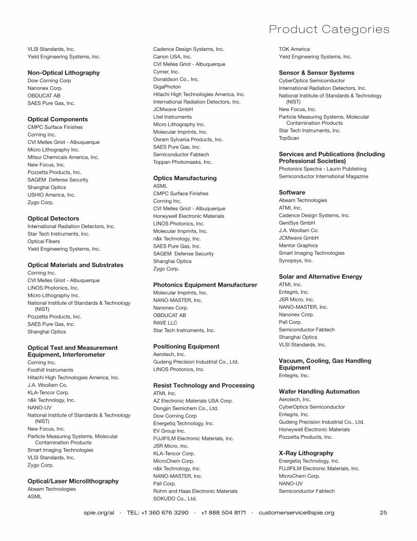
spie.org/al · TEL: +1 360 676 3290 · +1 888 504 8171 · [email protected] 25
VLSI Standards, Inc.Yield Engineering Systems, Inc.
Non-Optical LithographyDow Corning CorpNanonex Corp.OBDUCAT ABSAES Pure Gas, Inc.
Optical ComponentsCMPC Surface FinishesCorning Inc.CVI Melles Griot - AlbuquerqueMicro Lithography Inc.Mitsui Chemicals America, Inc.New Focus, Inc.Pozzetta Products, Inc.SAGEM Defense SecurityShanghai OpticsUSHIO America, Inc.Zygo Corp.
Optical DetectorsInternational Radiation Detectors, Inc.Star Tech Instruments, Inc.Optical FibersYield Engineering Systems, Inc.
Optical Materials and SubstratesCorning Inc.CVI Melles Griot - AlbuquerqueLINOS Photonics, Inc.Micro Lithography Inc.National Institute of Standards & Technology
(NIST)Pozzetta Products, Inc.SAES Pure Gas, Inc.Shanghai Optics
Optical Test and Measurement Equipment, InterferometerCorning Inc.Foothill InstrumentsHitachi High Technologies America, Inc.J.A. Woollam Co.KLA-Tencor Corp.n&k Technology, Inc.NANO-UVNational Institute of Standards & Technology
(NIST)New Focus, Inc.Particle Measuring Systems, Molecular
Contamination ProductsSmart Imaging TechnologiesVLSI Standards, Inc.Zygo Corp.
Optical/Laser MicrolithographyAbeam TechnologiesASML
Cadence Design Systems, Inc.Canon USA, Inc.CVI Melles Griot - AlbuquerqueCymer, Inc.Donaldson Co., Inc.GigaPhoton Hitachi High Technologies America, Inc.International Radiation Detectors, Inc.JCMwave GmbHLitel InstrumentsMicro Lithography Inc.Molecular Imprints, Inc.Osram Sylvania Products, Inc.SAES Pure Gas, Inc.Semiconductor FabtechToppan Photomasks, Inc.
Optics ManufacturingASMLCMPC Surface FinishesCorning Inc.CVI Melles Griot - AlbuquerqueHoneywell Electronic MaterialsLINOS Photonics, Inc.Molecular Imprints, Inc.n&k Technology, Inc.SAES Pure Gas, Inc.SAGEM Defense SecurityShanghai OpticsZygo Corp.
Photonics Equipment ManufacturerMolecular Imprints, Inc.NANO-MASTER, Inc.Nanonex Corp.OBDUCAT ABRAVE LLCStar Tech Instruments, Inc.
Positioning EquipmentAerotech, Inc.Gudeng Precision Industrial Co., Ltd.LINOS Photonics, Inc.
Resist Technology and ProcessingATMI, Inc.AZ Electronic Materials USA Corp.Dongjin Semichem Co., Ltd.Dow Corning CorpEnergetiq Technology, Inc.EV Group Inc.FUJIFILM Electronic Materials, Inc.JSR Micro, Inc.KLA-Tencor Corp.MicroChem Corp.n&k Technology, Inc.NANO-MASTER, Inc.Pall Corp.Rohm and Haas Electronic MaterialsSOKUDO Co., Ltd.
TOK AmericaYield Engineering Systems, Inc.
Sensor & Sensor SystemsCyberOptics SemiconductorInternational Radiation Detectors, Inc.National Institute of Standards & Technology
(NIST)New Focus, Inc.Particle Measuring Systems, Molecular
Contamination ProductsStar Tech Instruments, Inc.TopScan
Services and Publications (Including Professional Societies)Photonics Spectra - Laurin PublishingSemiconductor International Magazine
SoftwareAbeam TechnologiesATMI, Inc.Cadence Design Systems, Inc.GenISys GmbH J.A. Woollam Co.JCMwave GmbHMentor GraphicsSmart Imaging TechnologiesSynopsys, Inc.
Solar and Alternative EnergyATMI, Inc.Entegris, Inc.JSR Micro, Inc.NANO-MASTER, Inc.Nanonex Corp.Pall Corp.Semiconductor FabtechShanghai OpticsVLSI Standards, Inc.
Vacuum, Cooling, Gas Handling EquipmentEntegris, Inc.
Wafer Handling AutomationAerotech, Inc.CyberOptics SemiconductorEntegris, Inc.Gudeng Precision Industrial Co., Ltd.Honeywell Electronic MaterialsPozzetta Products, Inc.
X-Ray LithographyEnergetiq Technology, Inc.FUJIFILM Electronic Materials, Inc.MicroChem Corp.NANO-UVSemiconductor Fabtech
Product Categor ies
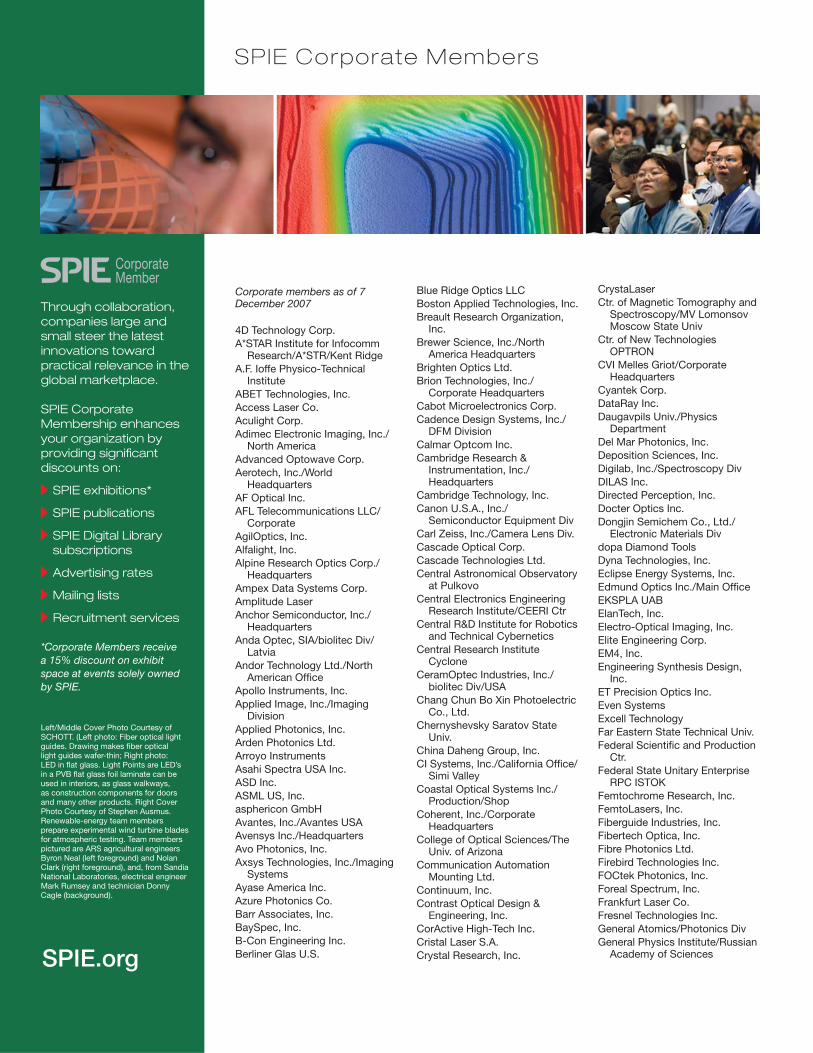
26 spie.org/al · TEL: +1 360 676 3290 · +1 888 504 8171 · [email protected]
Corporate members as of 7 December 2007
4D Technology Corp.A*STAR Institute for Infocomm
Research/A*STR/Kent RidgeA.F. Ioffe Physico-Technical
InstituteABET Technologies, Inc.Access Laser Co.Aculight Corp.Adimec Electronic Imaging, Inc./
North AmericaAdvanced Optowave Corp.Aerotech, Inc./World
HeadquartersAF Optical Inc.AFL Telecommunications LLC/
CorporateAgilOptics, Inc.Alfalight, Inc.Alpine Research Optics Corp./
HeadquartersAmpex Data Systems Corp.Amplitude LaserAnchor Semiconductor, Inc./
HeadquartersAnda Optec, SIA/biolitec Div/
LatviaAndor Technology Ltd./North
American Offi ceApollo Instruments, Inc.Applied Image, Inc./Imaging
DivisionApplied Photonics, Inc.Arden Photonics Ltd.Arroyo InstrumentsAsahi Spectra USA Inc.ASD Inc.ASML US, Inc.asphericon GmbHAvantes, Inc./Avantes USAAvensys Inc./HeadquartersAvo Photonics, Inc.Axsys Technologies, Inc./Imaging
SystemsAyase America Inc.Azure Photonics Co.Barr Associates, Inc.BaySpec, Inc.B-Con Engineering Inc.Berliner Glas U.S.SPIE.org
Left/Middle Cover Photo Courtesy of SCHOTT. (Left photo: Fiber optical light guides. Drawing makes fi ber optical light guides wafer-thin; Right photo: LED in fl at glass. Light Points are LED’s in a PVB fl at glass foil laminate can be used in interiors, as glass walkways, as construction components for doors and many other products. Right Cover Photo Courtesy of Stephen Ausmus. Renewable-energy team members prepare experimental wind turbine blades for atmospheric testing. Team members pictured are ARS agricultural engineers Byron Neal (left foreground) and Nolan Clark (right foreground), and, from Sandia National Laboratories, electrical engineer Mark Rumsey and technician Donny Cagle (background).
Through collaboration, companies large and small steer the latest innovations toward practical relevance in the global marketplace.
SPIE Corporate Membership enhances your organization by providing signifi cant discounts on:
SPIE exhibitions*
SPIE publications
SPIE Digital Library subscriptions
Advertising rates
Mailing lists
Recruitment services
*Corporate Members receive a 15% discount on exhibit space at events solely owned by SPIE.
Blue Ridge Optics LLCBoston Applied Technologies, Inc.Breault Research Organization,
Inc.Brewer Science, Inc./North
America HeadquartersBrighten Optics Ltd.Brion Technologies, Inc./
Corporate HeadquartersCabot Microelectronics Corp.Cadence Design Systems, Inc./
DFM DivisionCalmar Optcom Inc.Cambridge Research &
Instrumentation, Inc./Headquarters
Cambridge Technology, Inc.Canon U.S.A., Inc./
Semiconductor Equipment DivCarl Zeiss, Inc./Camera Lens Div.Cascade Optical Corp.Cascade Technologies Ltd.Central Astronomical Observatory
at PulkovoCentral Electronics Engineering
Research Institute/CEERI CtrCentral R&D Institute for Robotics
and Technical CyberneticsCentral Research Institute
CycloneCeramOptec Industries, Inc./
biolitec Div/USAChang Chun Bo Xin Photoelectric
Co., Ltd.Chernyshevsky Saratov State
Univ.China Daheng Group, Inc.CI Systems, Inc./California Offi ce/
Simi ValleyCoastal Optical Systems Inc./
Production/ShopCoherent, Inc./Corporate
HeadquartersCollege of Optical Sciences/The
Univ. of ArizonaCommunication Automation
Mounting Ltd.Continuum, Inc.Contrast Optical Design &
Engineering, Inc.CorActive High-Tech Inc.Cristal Laser S.A.Crystal Research, Inc.
CrystaLaserCtr. of Magnetic Tomography and
Spectroscopy/MV Lomonsov Moscow State Univ
Ctr. of New Technologies OPTRON
CVI Melles Griot/Corporate Headquarters
Cyantek Corp.DataRay Inc.Daugavpils Univ./Physics
DepartmentDel Mar Photonics, Inc.Deposition Sciences, Inc.Digilab, Inc./Spectroscopy DivDILAS Inc.Directed Perception, Inc.Docter Optics Inc.Dongjin Semichem Co., Ltd./
Electronic Materials Divdopa Diamond ToolsDyna Technologies, Inc.Eclipse Energy Systems, Inc.Edmund Optics Inc./Main Offi ceEKSPLA UABElanTech, Inc.Electro-Optical Imaging, Inc.Elite Engineering Corp.EM4, Inc.Engineering Synthesis Design,
Inc.ET Precision Optics Inc.Even SystemsExcell TechnologyFar Eastern State Technical Univ.Federal Scientifi c and Production
Ctr.Federal State Unitary Enterprise
RPC ISTOKFemtochrome Research, Inc.FemtoLasers, Inc.Fiberguide Industries, Inc.Fibertech Optica, Inc.Fibre Photonics Ltd.Firebird Technologies Inc.FOCtek Photonics, Inc.Foreal Spectrum, Inc.Frankfurt Laser Co.Fresnel Technologies Inc.General Atomics/Photonics DivGeneral Physics Institute/Russian
Academy of Sciences
SPIE Corporate Members
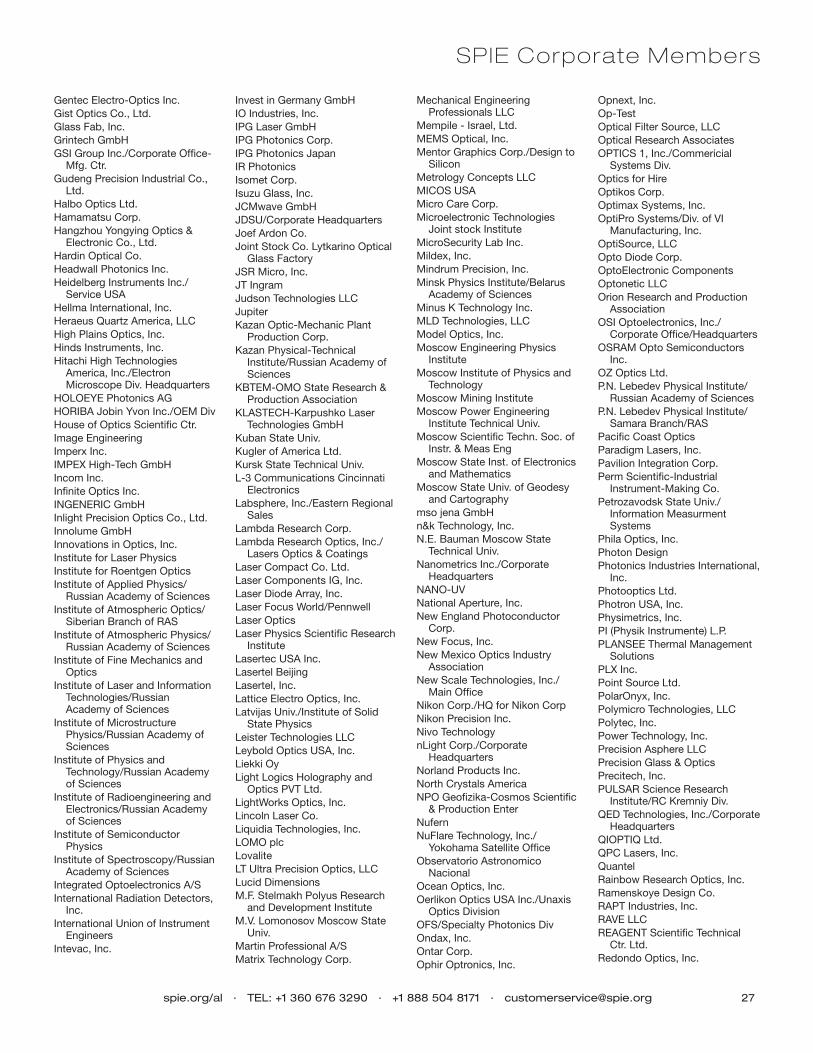
spie.org/al · TEL: +1 360 676 3290 · +1 888 504 8171 · [email protected] 27
SPIE Corporate Members
Gentec Electro-Optics Inc.Gist Optics Co., Ltd.Glass Fab, Inc.Grintech GmbHGSI Group Inc./Corporate Offi ce-
Mfg. Ctr.Gudeng Precision Industrial Co.,
Ltd.Halbo Optics Ltd.Hamamatsu Corp.Hangzhou Yongying Optics &
Electronic Co., Ltd.Hardin Optical Co.Headwall Photonics Inc.Heidelberg Instruments Inc./
Service USAHellma International, Inc.Heraeus Quartz America, LLCHigh Plains Optics, Inc.Hinds Instruments, Inc.Hitachi High Technologies
America, Inc./Electron Microscope Div. Headquarters
HOLOEYE Photonics AGHORIBA Jobin Yvon Inc./OEM DivHouse of Optics Scientifi c Ctr.Image EngineeringImperx Inc.IMPEX High-Tech GmbHIncom Inc.Infi nite Optics Inc.INGENERIC GmbHInlight Precision Optics Co., Ltd.Innolume GmbHInnovations in Optics, Inc.Institute for Laser PhysicsInstitute for Roentgen OpticsInstitute of Applied Physics/
Russian Academy of SciencesInstitute of Atmospheric Optics/
Siberian Branch of RASInstitute of Atmospheric Physics/
Russian Academy of SciencesInstitute of Fine Mechanics and
OpticsInstitute of Laser and Information
Technologies/Russian Academy of Sciences
Institute of Microstructure Physics/Russian Academy of Sciences
Institute of Physics and Technology/Russian Academy of Sciences
Institute of Radioengineering and Electronics/Russian Academy of Sciences
Institute of Semiconductor Physics
Institute of Spectroscopy/Russian Academy of Sciences
Integrated Optoelectronics A/SInternational Radiation Detectors,
Inc.International Union of Instrument
EngineersIntevac, Inc.
Invest in Germany GmbHIO Industries, Inc.IPG Laser GmbHIPG Photonics Corp.IPG Photonics JapanIR PhotonicsIsomet Corp.Isuzu Glass, Inc.JCMwave GmbHJDSU/Corporate HeadquartersJoef Ardon Co.Joint Stock Co. Lytkarino Optical
Glass FactoryJSR Micro, Inc.JT IngramJudson Technologies LLCJupiterKazan Optic-Mechanic Plant
Production Corp.Kazan Physical-Technical
Institute/Russian Academy of Sciences
KBTEM-OMO State Research & Production Association
KLASTECH-Karpushko Laser Technologies GmbH
Kuban State Univ.Kugler of America Ltd.Kursk State Technical Univ.L-3 Communications Cincinnati
ElectronicsLabsphere, Inc./Eastern Regional
SalesLambda Research Corp.Lambda Research Optics, Inc./
Lasers Optics & CoatingsLaser Compact Co. Ltd.Laser Components IG, Inc.Laser Diode Array, Inc.Laser Focus World/PennwellLaser OpticsLaser Physics Scientifi c Research
InstituteLasertec USA Inc.Lasertel BeijingLasertel, Inc.Lattice Electro Optics, Inc.Latvijas Univ./Institute of Solid
State PhysicsLeister Technologies LLCLeybold Optics USA, Inc.Liekki OyLight Logics Holography and
Optics PVT Ltd.LightWorks Optics, Inc.Lincoln Laser Co.Liquidia Technologies, Inc.LOMO plcLovaliteLT Ultra Precision Optics, LLCLucid DimensionsM.F. Stelmakh Polyus Research
and Development InstituteM.V. Lomonosov Moscow State
Univ.Martin Professional A/SMatrix Technology Corp.
Mechanical Engineering Professionals LLC
Mempile - Israel, Ltd.MEMS Optical, Inc.Mentor Graphics Corp./Design to
SiliconMetrology Concepts LLCMICOS USAMicro Care Corp.Microelectronic Technologies
Joint stock InstituteMicroSecurity Lab Inc.Mildex, Inc.Mindrum Precision, Inc.Minsk Physics Institute/Belarus
Academy of SciencesMinus K Technology Inc.MLD Technologies, LLCModel Optics, Inc.Moscow Engineering Physics
InstituteMoscow Institute of Physics and
TechnologyMoscow Mining InstituteMoscow Power Engineering
Institute Technical Univ.Moscow Scientifi c Techn. Soc. of
Instr. & Meas EngMoscow State Inst. of Electronics
and MathematicsMoscow State Univ. of Geodesy
and Cartographymso jena GmbHn&k Technology, Inc.N.E. Bauman Moscow State
Technical Univ.Nanometrics Inc./Corporate
HeadquartersNANO-UVNational Aperture, Inc.New England Photoconductor
Corp.New Focus, Inc.New Mexico Optics Industry
AssociationNew Scale Technologies, Inc./
Main Offi ceNikon Corp./HQ for Nikon CorpNikon Precision Inc.Nivo TechnologynLight Corp./Corporate
HeadquartersNorland Products Inc.North Crystals AmericaNPO Geofi zika-Cosmos Scientifi c
& Production EnterNufernNuFlare Technology, Inc./
Yokohama Satellite Offi ceObservatorio Astronomico
NacionalOcean Optics, Inc.Oerlikon Optics USA Inc./Unaxis
Optics DivisionOFS/Specialty Photonics DivOndax, Inc.Ontar Corp.Ophir Optronics, Inc.
Opnext, Inc.Op-TestOptical Filter Source, LLCOptical Research AssociatesOPTICS 1, Inc./Commericial
Systems Div.Optics for HireOptikos Corp.Optimax Systems, Inc.OptiPro Systems/Div. of VI
Manufacturing, Inc.OptiSource, LLCOpto Diode Corp.OptoElectronic ComponentsOptonetic LLCOrion Research and Production
AssociationOSI Optoelectronics, Inc./
Corporate Offi ce/HeadquartersOSRAM Opto Semiconductors
Inc.OZ Optics Ltd.P.N. Lebedev Physical Institute/
Russian Academy of SciencesP.N. Lebedev Physical Institute/
Samara Branch/RASPacifi c Coast OpticsParadigm Lasers, Inc.Pavilion Integration Corp.Perm Scientifi c-Industrial
Instrument-Making Co.Petrozavodsk State Univ./
Information Measurment Systems
Phila Optics, Inc.Photon DesignPhotonics Industries International,
Inc.Photooptics Ltd.Photron USA, Inc.Physimetrics, Inc.PI (Physik Instrumente) L.P.PLANSEE Thermal Management
SolutionsPLX Inc.Point Source Ltd.PolarOnyx, Inc.Polymicro Technologies, LLCPolytec, Inc.Power Technology, Inc.Precision Asphere LLCPrecision Glass & OpticsPrecitech, Inc.PULSAR Science Research
Institute/RC Kremniy Div.QED Technologies, Inc./Corporate
HeadquartersQIOPTIQ Ltd.QPC Lasers, Inc.QuantelRainbow Research Optics, Inc.Ramenskoye Design Co.RAPT Industries, Inc.RAVE LLCREAGENT Scientifi c Technical
Ctr. Ltd.Redondo Optics, Inc.
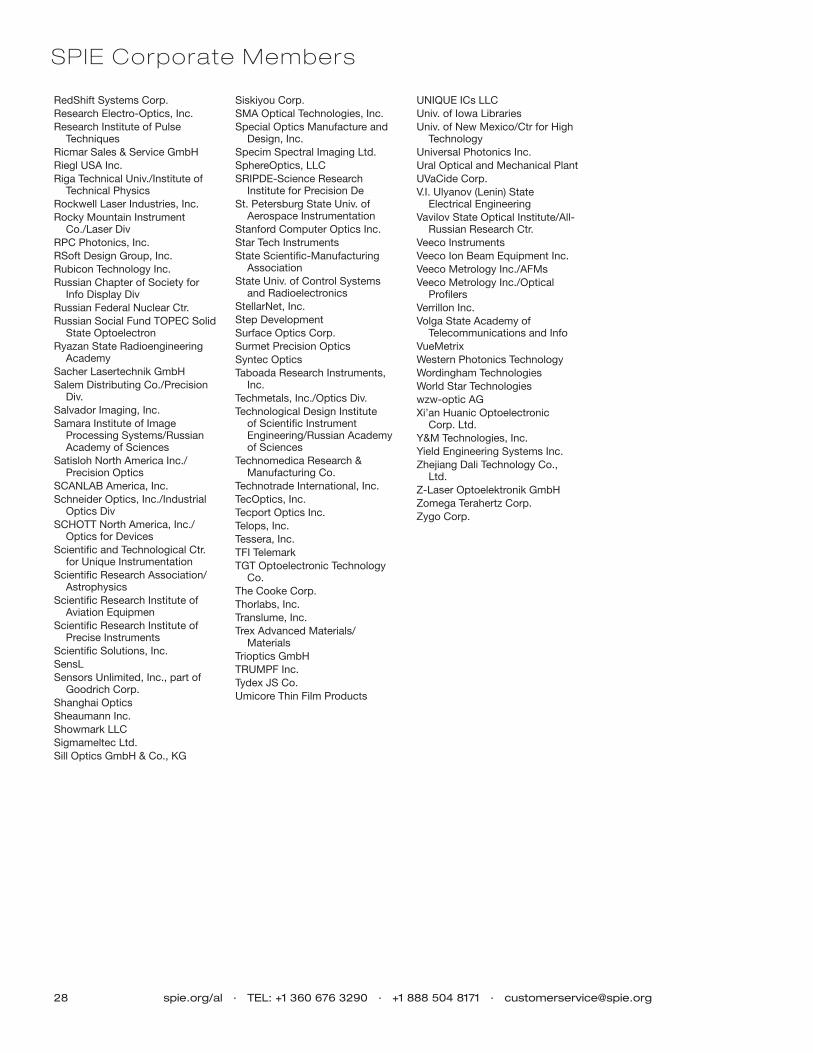
28 spie.org/al · TEL: +1 360 676 3290 · +1 888 504 8171 · [email protected]
RedShift Systems Corp.Research Electro-Optics, Inc.Research Institute of Pulse
TechniquesRicmar Sales & Service GmbHRiegl USA Inc.Riga Technical Univ./Institute of
Technical PhysicsRockwell Laser Industries, Inc.Rocky Mountain Instrument
Co./Laser DivRPC Photonics, Inc.RSoft Design Group, Inc.Rubicon Technology Inc.Russian Chapter of Society for
Info Display DivRussian Federal Nuclear Ctr.Russian Social Fund TOPEC Solid
State OptoelectronRyazan State Radioengineering
AcademySacher Lasertechnik GmbHSalem Distributing Co./Precision
Div.Salvador Imaging, Inc.Samara Institute of Image
Processing Systems/Russian Academy of Sciences
Satisloh North America Inc./Precision Optics
SCANLAB America, Inc.Schneider Optics, Inc./Industrial
Optics DivSCHOTT North America, Inc./
Optics for DevicesScientifi c and Technological Ctr.
for Unique InstrumentationScientifi c Research Association/
AstrophysicsScientifi c Research Institute of
Aviation EquipmenScientifi c Research Institute of
Precise InstrumentsScientifi c Solutions, Inc.SensLSensors Unlimited, Inc., part of
Goodrich Corp.Shanghai OpticsSheaumann Inc.Showmark LLCSigmameltec Ltd.Sill Optics GmbH & Co., KG
SPIE Corporate Members
Siskiyou Corp.SMA Optical Technologies, Inc.Special Optics Manufacture and
Design, Inc.Specim Spectral Imaging Ltd.SphereOptics, LLCSRIPDE-Science Research
Institute for Precision DeSt. Petersburg State Univ. of
Aerospace InstrumentationStanford Computer Optics Inc.Star Tech InstrumentsState Scientifi c-Manufacturing
AssociationState Univ. of Control Systems
and RadioelectronicsStellarNet, Inc.Step DevelopmentSurface Optics Corp.Surmet Precision OpticsSyntec OpticsTaboada Research Instruments,
Inc.Techmetals, Inc./Optics Div.Technological Design Institute
of Scientifi c Instrument Engineering/Russian Academy of Sciences
Technomedica Research & Manufacturing Co.
Technotrade International, Inc.TecOptics, Inc.Tecport Optics Inc.Telops, Inc.Tessera, Inc.TFI TelemarkTGT Optoelectronic Technology
Co.The Cooke Corp.Thorlabs, Inc.Translume, Inc.Trex Advanced Materials/
MaterialsTrioptics GmbHTRUMPF Inc.Tydex JS Co.Umicore Thin Film Products
UNIQUE ICs LLCUniv. of Iowa LibrariesUniv. of New Mexico/Ctr for High
TechnologyUniversal Photonics Inc.Ural Optical and Mechanical PlantUVaCide Corp.V.I. Ulyanov (Lenin) State
Electrical EngineeringVavilov State Optical Institute/All-
Russian Research Ctr.Veeco InstrumentsVeeco Ion Beam Equipment Inc.Veeco Metrology Inc./AFMsVeeco Metrology Inc./Optical
Profi lersVerrillon Inc.Volga State Academy of
Telecommunications and InfoVueMetrixWestern Photonics TechnologyWordingham TechnologiesWorld Star Technologieswzw-optic AGXi’an Huanic Optoelectronic
Corp. Ltd.Y&M Technologies, Inc.Yield Engineering Systems Inc.Zhejiang Dali Technology Co.,
Ltd.Z-Laser Optoelektronik GmbHZomega Terahertz Corp.Zygo Corp.
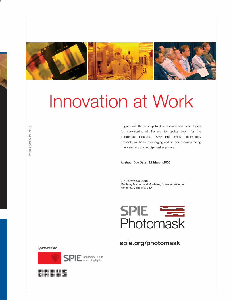
MRKT0983 SPIE07 Ad-2.ai 12/20/07 5:51:58 PM
spie.org/photomask
Innovation at WorkEngage with the most up-to-date research and technologies
for maskmaking at the premier global event for the
photomask industry. SPIE Photomask Technology
presents solutions to emerging and on-going issues facing
mask makers and equipment suppliers.
Abstract Due Date: 24 March 2008
6–10 October 2008Monterey Marriott and Monterey, Conference CenterMonterey, California, USA
Sponsored by
Pho
to c
ourt
esy
of:
AM
TC
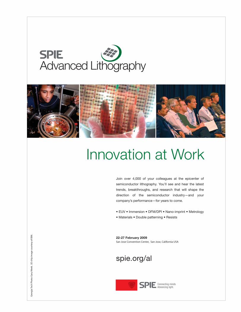
Join over 4,000 of your colleagues at the epicenter of
semiconductor lithography. You’ll see and hear the latest
trends, breakthroughs, and research that will shape the
direction of the semiconductor industry—and your
company’s performance—for years to come.
• EUV • Immersion • DFM/DPI • Nano-imprint • Metrology
• Materials • Double patterning • Resists
22-27 February 2009 San Jose Convention Center, San Jose, California USA
spie.org/al
Geo
rgia
Tec
h P
ho
to: G
ary
Mee
k. 3
D c
hip
imag
e co
urt
esy
of I
BM
.

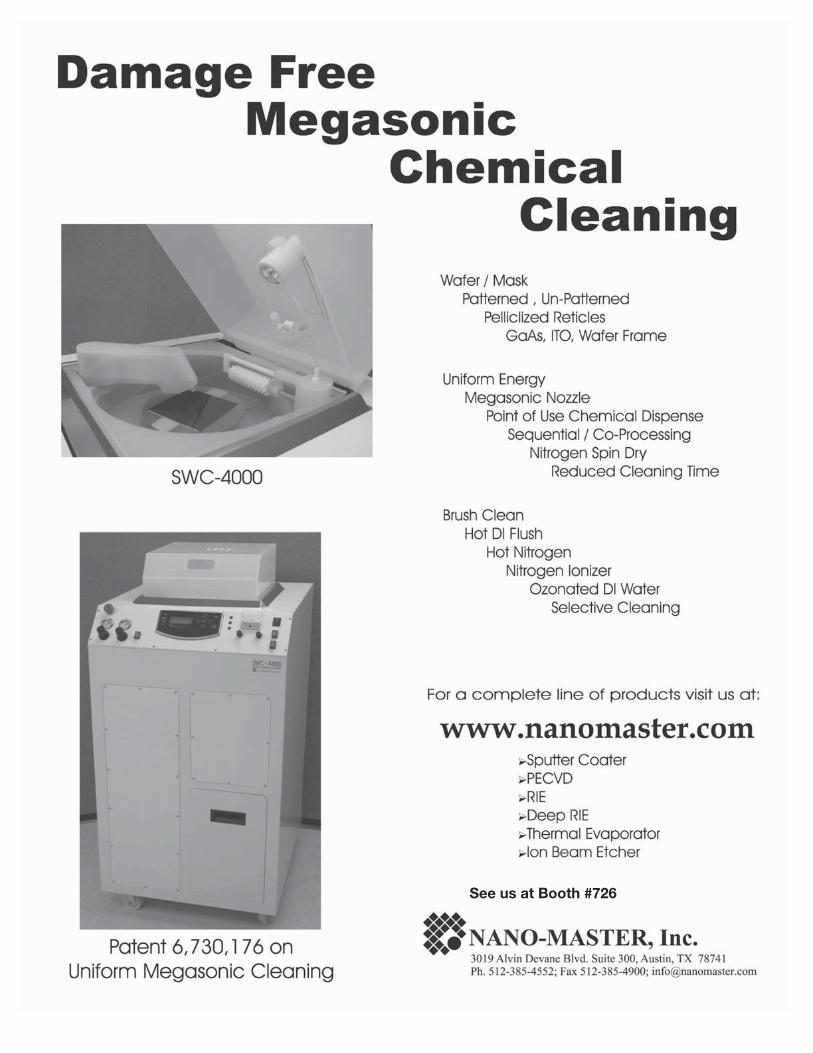


![Skinbones Exhibition Guide[1]](https://img.pdfslide.net/doc/110x75/5535c3015503462c748b475b/skinbones-exhibition-guide1.jpg)