Embed Size (px)
Citation preview

Copyright © JORJIN TECHNOLOGIES INC. 2012 http://WWW.JORJIN.COM.TW
CONFIDENTIAL
a module solution provider
WG1300-B0 WLAN Module
TI CC3000 IEEE 802.11b/g solution
Datasheet
Draft 0.2
JORJIN
CONFID
ENTIA
L

Doc No: WG1300-B0-DTS-D02
Copyright © JORJIN TECHNOLOGIES INC. 2012
http://WWW.JORJIN.COM.TW CONFIDENTIAL
Page 1
FEATURES DESCRIPTION IEEE 802.11 b/g compliant. WG1300-B0 is a 2.4GHz WLAN module which can
Compact footprint: 14.5mmx14.5mmx2mm be integrated with any low-cost/low power MCU
Operating Voltage: 2.9~4.8V to makes it the ideal solution for embedded
Operating temperature: -40~85°C applications.
Embedded Wi-Fi and networking software
Long range, reliable coverage throughout With the necessary PHY, MAC and network layers,
the entire house it makes WG1300-B0 can support WLAN
Proven Wi-Fi interoperability application via SPI bus to communicate with
Complete platform solution and certified host microcontrollers or other embedded
modules processors.
Get started quickly with sample applications With worldwide certificates, customers can
on multiple platforms leverage modular certificate by adopting the same
Comprehensive documentation and support antenna and RF trace routing to save
community development cost and speed up time to market by
Porting documentation available to allow following its reference design.
MCU flexibility
APPLICATIONS
Home entertainment control ● Remote storage devices
Thermostats, appliances ● Cameras and video surveillance
HVAC controller, remote displays ● Toys
Home Network aggregators ● Gaming
Remote appliance diagnostics/support
Including drivers, stack, and supplicant
Universal IP connectivity enabled anywhere
Pair easily with low-memory, low-cost,
Low-power microcontroller systems
Implement Wi-Fi quickly without previous
Wi-Fi or RF experience
Credible, proven solution with best-in-class
Budget
JORJIN
CONFID
ENTIA
L

Doc No: WG1300-B0-DTS-D02
Copyright © JORJIN TECHNOLOGIES INC. 2012
http://WWW.JORJIN.COM.TW CONFIDENTIAL
Page 2
Index
1. FUNCTIONAL FEATURES ........................................................................................................... 4
1.1. MODULE BLOCK DIAGRA ............................................................................................................ 4
1.2. FUNCTIONAL BLOCK FEATURES ........................................................................................ 4
1.2.1. WLAN Features……………………………………..…………………………………………….4
1.2.2. Network Stack Supported Protocols ................................................................................. 5
1.2.3. Wireless Security System Features .................................................................................... 5
2. MODULE SPECIFICATION ......................................................................................................... 6
2.1. ABSOLUTE MAXIMUM RATINGS ................................................................................................... 6
2.2. RECOMMENDED OPERATING CONDITIONS ................................................................................... 6
2.3. GENERAL CHARACTERISTICS ....................................................................................................... 7
3. MODULE OUTLINE....................................................................................................................... 8
3.1. FOOTPRINT AND PINOUTS ............................................................................................................. 8
3.2. PIN DESCRIPTION ....................................................................................................................... 11
4. SPI HOST CONTROLLER INTERFACE .................................................................................. 11
4.1. OVERVIEW ................................................................................................................................. 11
4.2. SPI INTERFACE DESCRIPTION .................................................................................................... 11
4.3. SPI LINE DESCRIPTION .............................................................................................................. 12
4.4. SPI TIMING ................................................................................................................................ 12
5. POWER-UP SEQUENCE ............................................................................................................. 14
6. DEBUG INTERFACE ................................................................................................................... 15
6.1.UART DEBUG LINES .................................................................................................................. 15
6.2.RS232 DEBUG LINES .................................................................................................................. 15
7. SMT AND BAKING RECOMMENDATIONS........................................................................... 16
7.1. BAKING CONDITION ................................................................................................................... 16
7.2. SMT RECOMMENDATION ........................................................................................................... 16
7.3. STENCIL THICKNESS ................................................................................................................... 17
7.4. SOLDERING PASTE (WITHOUT PB) ............................................................................................... 17
8. PACKAGE INFORMATION ........................................................................................................ 18
JORJIN
CONFID
ENTIA
L

Doc No: WG1300-B0-DTS-D02
Copyright © JORJIN TECHNOLOGIES INC. 2012
http://WWW.JORJIN.COM.TW CONFIDENTIAL
Page 3
8.1. MODULE MECHANICAL OUTLINE............................................................................................... 18
8.2. PACKAGE MARKING ................................................................................................................... 19
8.3.ORDERING INFORMATION ........................................................................................................... 19
9. REFERENCE SCHEMATICS ...................................................................................................... 20
10. LAYOUT RECOMMENDATIONS ............................................................................................ 21
11. CONTACT JORJIN TECHNOLOGY ....................................................................................... 23
12. HISTORY CHANGE ................................................................................................................... 24
JORJIN
CONFID
ENTIA
L

Doc No: WG1300-B0-DTS-D02
Copyright © JORJIN TECHNOLOGIES INC. 2012
http://WWW.JORJIN.COM.TW CONFIDENTIAL
Page 4
1. FUNCTIONAL FEATURES
1.1. Module Block Diagram
Figure 1 Module Block Diagram
1.2. Functional Block Feature
1.2.1. WLAN Features
WLAN MAC Baseband Processor and RF transceiver which is IEEE802.11b/g compliant
Accepts 26MHz reference clock Input
IEEE Std 802.11d,i PICS compliant
Supports Serial Peripheral Interface (SPI) Host Interface
Medium-Access Controller (MAC)
Embedded ARM™ Central Processing Unit (CPU)
Hardware-Based Encryption/Decryption Using 64-, 128-Bit WEP, TKIP or AES Keys
Supports requirements for Wireless Fidelity (Wi-Fi) Protected Access (WPA and
WPA2.0) and IEEE Std 802.11i [Includes Hardware-Accelerated Adanced-Encrytion
Standard (AES)]
JORJIN
CONFID
ENTIA
L

Doc No: WG1300-B0-DTS-D02
Copyright © JORJIN TECHNOLOGIES INC. 2012
http://WWW.JORJIN.COM.TW CONFIDENTIAL
Page 5
Baseband Processor
2.4GHz Radio
Digital Radio Processor (DRP) implementation
Internal LNA
Supports : IEEE Std 802.11b, 802.11g, 802.11b/g
1.2.2. Network Stack Supported Protocols
Transport layer
TCP
UDP
Network layer
IPv4
Ping
DHCP
DNS Client
Link layer
ARP
1.2.3. Wireless Security System Features
Supported modes
Open (no security)
WEP
WPA-Personal
WPA2-Personal
Supported encryption types
WEP
TKIP
AES
Open
JORJIN
CONFID
ENTIA
L

Doc No: WG1300-B0-DTS-D02
Copyright © JORJIN TECHNOLOGIES INC. 2012
http://WWW.JORJIN.COM.TW CONFIDENTIAL
Page 6
2. MODULE SPECIFICATION
2.1. Absolute Maximum Ratings
Parameters Min Max Unit
Power supply Voltage (VBAT_IN) –0.5 +5.5 (1) V
Voltage of digital pins (2) –0.5 +3.6 V
Voltage of EEPROM and RS232 test signals –0.5 2.1 V
Operating Temperature –40 +85 (3) °C
Storage Temperature –55 +125 °C
(1) Maximum allowed depends on accumulated time at that voltage; 4.8V for 7 years lifetime,5.5V for
6 hours cumulative.
(2) This includes the SPI and Power Enable signals
(3) The device can be reliably operated for 5,000 active-WLAN cumulative hours at TA of 85°C.
Table 1 Absolute Maximum Ratings
2.2. Recommended Operating Conditions Recommended Operating Conditions
Parameters Min TYP Max Unit
VBAT_IN 2.9 3.3 4.8 V
Voltage of digital pins 0 3.3 3.6 V
Voltage of EEPROM and RS232 test signals 0 1.8 V
Operating Temperature –30 25 75 °C
Table 2 Recommended Operating Conditions
JORJIN
CONFID
ENTIA
L

Doc No: WG1300-B0-DTS-D02
Copyright © JORJIN TECHNOLOGIES INC. 2012
http://WWW.JORJIN.COM.TW CONFIDENTIAL
Page 7
2.3. General Characteristics DC Characteristics (RS232/EEPROM I/O)
Parameters Test Conditions Min Max Unit
Logic input low, VIL -- 0 0.67 V
Logic input high, VIH -- 1.05 1.92 V
Logic output low, VOL 4.8mA 0 0.45 V
Logic output high, VOH 4.8mA 1.17 1.92 V
Table 3 DC Characteristics General Purpose I/O
JORJIN
CONFID
ENTIA
L

Doc No: WG1300-B0-DTS-D02
Copyright © JORJIN TECHNOLOGIES INC. 2012
http://WWW.JORJIN.COM.TW CONFIDENTIAL
Page 8
3. MODULE OUTLINE
3.1. Footprint and pinouts
For PCB layout, the footprint below is recommended for your applications.
Figure 2 WG1300-B0 Footprint and Pinouts
3.2. Pin Description
Pin # Signal Name Type Description
1 GND GND Ground
2 WL_UART_DBG I WL_UART_DBG
3 WL_EN2 (1) O WL_EN2
4 WL_EN1 (2) O WL_EN1.
5 WL_RS232_TX (3) I WL_RS232_TX (Test-mode signal, 1.8V Logic)
6 WL_RS232_RX (3) O WL_RS232_RX (Test-mode signal, 1.8V Logic)
7 GND GND Ground
8 VIO_SOC Power Module VIO Supply
9 GND GND Ground
Unit: mm
JORJIN
CONFID
ENTIA
L

Doc No: WG1300-B0-DTS-D02
Copyright © JORJIN TECHNOLOGIES INC. 2012
http://WWW.JORJIN.COM.TW CONFIDENTIAL
Page 9
10 GND GND Ground
11 SPI_DIN I HOST Interface SPI Data In
12 SPI_DOUT I HOST Interface SPI Data Out
13 SPI_IRQ O HOST Interface SPI Interrupt
14 SPI_CLK O HOST Interface SPI CLOCK
15 SPI_CS O HOST Interface SPI Chip Select
16 GND GND Ground
17 EXT_32K CLK EXTERNAL SLOW CLOCK FROM HOST
18 GND GND Ground
19 GND GND Ground
20 XTALP Fref Input
21 XTALM Fref Input
22 GND GND Ground
23 SCL_EEPROM (4) I/O I2C CLOCK LINE FROM EEPROM.
24 SCL_CC3000 (4) I/O I2C CLOCK LINE FROM CC3000.
25 SDA_EEPROM (5) I/O I2C DATA LINE FROM EEPROM.
26 SDA_CC3000 (5) I/O I2C DATA LINE FROM CC3000.
27 GND GND Ground
28 VBAT_IN Power Power Supply to Module
29 GND GND Ground
30 DC2DC_OUT I 1.8V Supply
31 GND GND Ground
32 CLK_REQ_OUT I/O Clock request out
33 NS_UARTD I/O Networking subsystem; UART Debug line
34 GND GND Ground
35 RF_ANT RF WLAN ANT Port
36 GND GND Ground
37 GND GND Ground
38 GND GND Ground
JORJIN
CONFID
ENTIA
L

Doc No: WG1300-B0-DTS-D02
Copyright © JORJIN TECHNOLOGIES INC. 2012
http://WWW.JORJIN.COM.TW CONFIDENTIAL
Page 10
39 GND GND Ground
40 GND GND Ground
41 GND GND Ground
42 GND GND Ground
43 GND GND Ground
44 GND GND Ground
45 GND GND Ground
46 GND GND Ground
47 GND GND Ground
48 GND GND Ground
49 GND GND Ground
50 GND GND Ground
51 GND GND Ground
(1) Short to WL_EN1 (Pin #7) for function mode.
(2) Short to GND for test mode; Short to WL_EN2 (Pin #5) for function mode.
(3) Left unconnected for function mode
(4) I2C Clock lines from EEPROM and CC3000 must be connected together for function mode.
(5) I2C Data lines from EEPROM and CC3000 must be connected together for function mode.
Table 4 WG1300-B0 Pin Description
JORJIN
CONFID
ENTIA
L

Doc No: WG1300-B0-DTS-D02
Copyright © JORJIN TECHNOLOGIES INC. 2012
http://WWW.JORJIN.COM.TW CONFIDENTIAL
Page 11
4. SPI HOST CONTROLLER INTERFACE
WG1300-B0 communicates with HOST via SPI Bus. Below shows the descriptions on SPI bus.
4.1. Overview
The SPI interface provides high-speed data transfer capability with low power consumption for
mobile electronic devices. The SPI bus was designed to operate on a point-to-multipoint basis
by providing a separate, active-low chip select (CS) per device.
4.2. SPI Interface Description
In order to facilitate a broad implementation, the protocol is half duplex and does not require
simultaneous operation of data OUT (DO) and data IN (DI). All TI communication devices are
slaves in this protocol, and all transactions are initiated by the host, as the SPI Master. The
clock rate for each one of the connected devices may be different and configured per device.
Figure 3 shows SPI interface signals
Figure 3 SPI Interface signals
JORJIN
CONFID
ENTIA
L

Doc No: WG1300-B0-DTS-D02
Copyright © JORJIN TECHNOLOGIES INC. 2012
http://WWW.JORJIN.COM.TW CONFIDENTIAL
Page 12
4.3. SPI Line Description
Port Name I/O Description
SPI_CLK I Clock (0 MHz to 38.4 MHz) from host to slave
SPI_DI I Data from host to slave
SPI_CS(1) I CS signal from host to slave
SPI_IRQ(2) O Interrupt from slave to host
SPI_DO O Data from slave to host
(1) CS selects a CC3000 device, indicating that a master wants to communicate to the device. (2) IRQ is a dual-purpose slave to the master direction line: in SPI IDLE state while no data transfer
is active, driving IRQ low indicates to the master that the CC3000 device has data to pass to it;
driving IRQ low following CS deassertion indicates that the CC3000 device is ready to receive data.
Table 5 SPI Interface Signals Description
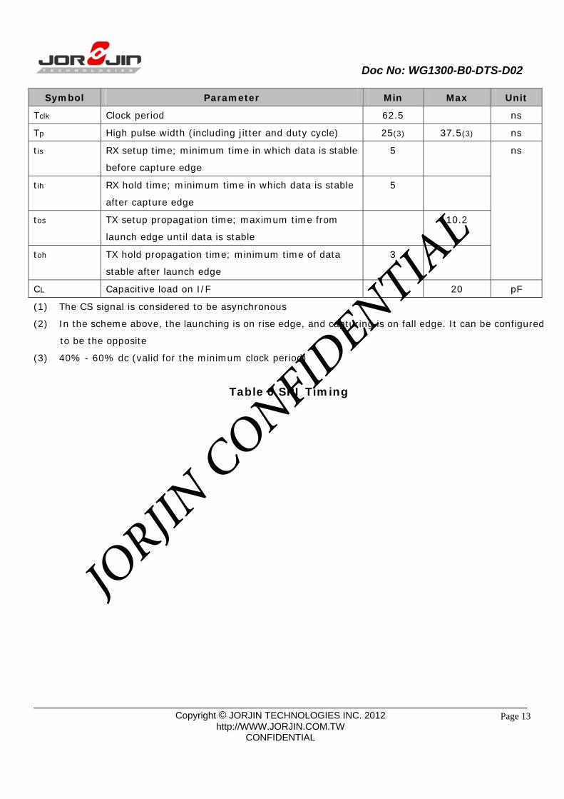
4.4. SPI Timing
Figure 4 SPI Timing
JORJIN
CONFID
ENTIA
L
Doc No: WG1300-B0-DTS-D02
Copyright © JORJIN TECHNOLOGIES INC. 2012
http://WWW.JORJIN.COM.TW CONFIDENTIAL
Page 13
(1) The CS signal is considered to be asynchronous
(2) In the scheme above, the launching is on rise edge, and capturing is on fall edge. It can be configured
to be the opposite
(3) 40% - 60% dc (valid for the minimum clock period)
Table 6 SPI Timing
Symbol Parameter Min Max Unit
Tclk Clock period 62.5 ns
Tp High pulse width (including jitter and duty cycle) 25(3) 37.5(3) ns
tis RX setup time; minimum time in which data is stable
before capture edge
5 ns
tih RX hold time; minimum time in which data is stable
after capture edge
5
tos TX setup propagation time; maximum time from
launch edge until data is stable
10.2
toh TX hold propagation time; minimum time of data
stable after launch edge
3
CL Capacitive load on I/F 20 pF
JORJIN
CONFID
ENTIA
L

Doc No: WG1300-B0-DTS-D02
Copyright © JORJIN TECHNOLOGIES INC. 2012
http://WWW.JORJIN.COM.TW CONFIDENTIAL
Page 14
5. POWER-UP SEQUENCE
Figure 7 demonstrates the wake up sequence of WG1300-B0
Figure 5 WG1300-B0 Power-On Sequences
Note: 1. VBAT_IN, VIO, and SLOWCLK must be available before WL_EN1 and WL_EN2 are asserted.
2. At T0: WL_EN1 and WL_EN2 can be asserted after the VIO reaches 90 percent of VIO voltage.
On this functional mode the MCU drives the WLAN pins to initiate the power up (WL_EN1 and
WL_EN2 are shorted and connected to MCU GPIO).
3. At T1 (wake-up time): The CC3000 device accomplishes power up after the IRQ changes state to
LOW. Wake-up time T1 is approximately 53 msec.
4. At T2: The normal master SPI write sequence is CS low, followed by IRQ low (CC3000 host),
indicating that the CC3000 core device is ready to accept data. The duration of T2
is approximately 7 msec.
JORJIN
CONFID
ENTIA
L
Doc No: WG1300-B0-DTS-D02
Copyright © JORJIN TECHNOLOGIES INC. 2012
http://WWW.JORJIN.COM.TW CONFIDENTIAL
Page 15
6. DEBUG INTERFACE
The debug interface helps customers to evaluate the HW/SW features for their application. It also helps to
debug during the development and manufacturing stage. The WG1300-B0 module support RS232 signals
and UART signals for debug purpose. Connect RS232 and UART signals to the test points for future debug
support.
6.1. UART Debug Lines
A unidirectional UART lines are provided for debugging WLAN subsystem and network subsystem
functions. This is a TX-only debug interface that delivers diagnostic messages. Table 11 shows the
dedicated UART debug pins of WG1300-B0
Signal names WG1300-B0 Pin# Function
WL_UART_DBG 4 Logger for WLAN FW debug
NS_UARTD 2 Networking subsystem UART Debug line
Table 7 WG1300-B0 UART Debug Lines
6.2. RS232 Debug Lines
During production testing the pins below are used for RTTT Wireless LAN SW utility. Table 12
shows the dedicated rs232 debug pins of WG1300-B0
Signal names Function
WL_RS232_TX RTTT Test Utility for WLAN RF Debug
WL_RS232_RX
Table 8 WG1300-B0 RS232 Debug Lines
JORJIN
CONFID
ENTIA
L

Doc No: WG1300-B0-DTS-D02
Copyright © JORJIN TECHNOLOGIES INC. 2012
http://WWW.JORJIN.COM.TW CONFIDENTIAL
Page 16
7. SMT AND BAKING RCOMMENDATIONS
7.1. Baking Condition
Follow MSL Level 4 to do baking process.
After bag is opened, devices that will be subjected to reflow solder or other high temperature process
must be mounted within 72 hours of factory conditions <30°C/60% RH or stored at <10% RH.
Device require bake, before mounting, if Humidity Indicator Card reads > 10%
If baking is required, Devices may be baked for 8 hrs at 125°C.
7.2. SMT Recommendation
Figure 8 is recommended reflow profile and Table 13 is its information
H
Figure 6 WG1300-B0 Recommended reflow profile
JORJIN
CONFID
ENTIA
L

Doc No: WG1300-B0-DTS-D02
Copyright © JORJIN TECHNOLOGIES INC. 2012
http://WWW.JORJIN.COM.TW CONFIDENTIAL
Page 17
No. Item Temperature (°C) Time (sec) 1 Pre-heat D1: 140 ~ D2: 200 T1: 80 ~ 120
2 Soldering D2: = 220 T2: 60 +/- 10
3 Peak-Temp. D3: 250 °C max
Table 9 WG1300-B0 reflow information
Note: (1) Reflow soldering is recommended two times maximum. (2) Add Nitrogen while Reflow process: SMT solder ability will be better.
7.3. Stencil Thickness
0.1~ 0.15 mm (Recommended)
7.4. Soldering Paste (without Pb)
Recommended SENJU N705-GRN3360-K2-V can get better soldering effects.
JO
RJIN C
ONFIDEN
TIAL

Doc No: WG1300-B0-DTS-D02
Copyright © JORJIN TECHNOLOGIES INC. 2012
http://WWW.JORJIN.COM.TW CONFIDENTIAL
Page 18
8. PACKAGE INFORMATION
8.1. Module Mechanical Outline
Figure 7 WG1300-B0 Mechanical Outline
JORJIN
CONFID
ENTIA
L

Doc No: WG1300-B0-DTS-D02
Copyright © JORJIN TECHNOLOGIES INC. 2012
http://WWW.JORJIN.COM.TW CONFIDENTIAL
Page 19
8.2. Package Marking
Date Code: YYWWSSF
YY = Digit of the year, ex: 2010=10
WW = Week (01~53)
SS = Serial number from 01 ~99 match to manufacture’s lot number
F = Reserve for internal use
Figure 8 WG1300-B0 Package Marking
8.3. Ordering Informaiton
Order Number Description
WG1300-B0 JORJIN CC3000 Module
Table 10 Orderable WG1300-B0 Part Numbers
JORJIN
CONFID
ENTIA
L

Doc No: WG1300-B0-DTS-D02
Copyright © JORJIN TECHNOLOGIES INC. 2012
http://WWW.JORJIN.COM.TW CONFIDENTIAL
Page 20
9. REFERENCE SCHEMATICS
Host Interface level recommend:
VIO_SYS
To 1V8 Host Level
To VIO_SYS Host Level
VIO_SYS
U1WG1300-B0E_N51_14.5X14.5_1.3
WL_
UA
RT
_DB
G2
NS_UARTD33
WL_
EN
14
WL_
EN
23
WL_
RS
232_
TX
5
WL_
RS
232_
RX
6
EXT_32K17
GND36
SC
L_C
C30
0024
SC
L_E
EP
RO
M23
SD
A_C
C30
0026
SD
A_E
EP
RO
M25
SPI_IRQ13
SPI_DOUT12
SPI_CS15
SPI_CLK14
SPI_DIN11
RF_ANT35
DC2DC_OUT30
GN
D27
GN
D1
GN
D9
GN
D37
GN
D38
GN
D39
GN
D40
GND16
VBAT_IN28
GND31
GN
D7
VIO
_SO
C8
GN
D19
GND34
GN
D41
GN
D42
GN
D43
GN
D51
GN
D50
GN
D49
GN
D48
GN
D44
GN
D45
GN
D46
GN
D47
XT
ALM
21
XT
ALP
20
GND18
GND29
GND10
GN
D22
CLK_REQ_OUT32
VBAT_SYS: 2.7V~4.8V => 3.6V TYP
VIO_SOC: 1.62V~1.92V => 1.8V TYP
C3NL_10pFCAP1005
J1U.FL-R-SMT(10)U.FL
12
3
L2NLIND1005
C110pFCAP1005
L1NLIND1005
C210pF
CAP1005
ANT1AT8010-E2R9HAA8.0x1.0x1.0mm
1
2
The Antenna matching circuit.
R6 0R RES1005
VBAT_IN
VBAT_IN
VBAT_SW_EN
U2SN74AVC2T45XBGA-N8_1X2_0.5-A
VCCA1
A12
A23
GND4
VCCB8
B17
B26
DIR5
VIO_SOC
VIO LDO
U4SN74AVC2T45XBGA-N8_1X2_0.5-A
VCCA1
A12
A23
GND4
VCCB8
B17
B26
DIR5
TP1
R17 0RRES1005
WL_SPI_IRQ_1V8WL_SPI_DOUT_1V8
U5SN74AVC2T45XBGA-N8_1X2_0.5-A
VCCA1
A12
A23
GND4
VCCB8
B17
B26
DIR5
WL_SPI_CS_1V8
U6TPS22913BXBGA-N4_0.9x0.9_0.5
VINA2
VOUTA1
ONB2
GNDB1
VBAT_IN
U3TPS79718MO-203_2.1x2
GND2
NC3
IN4
OUT5
PG1
R9 0R RES1005
WL_SPI_DOUT_HOSTWL_SPI_IRQ_HOST
VIO_SYS: Voltage of Host Level
-->
C61uF
CAP1005R18100KRES1005
-->
VIO_SOC
C40.47uFCAP1005
-->
DIR High : A data to B busDIR Low : B data to A bus
VIO_SYS R15100KRES1005
WG1300-B0 MODULE
VBAT_SYS
C5 1uFCAP1005
WL_SPI_DIN_HOSTWL_SPI_CLK_HOST
WL_SPI_CS_HOST
WL_SPI_DIN_1V8WL_SPI_CLK_1V8
VBAT_SYS FET SWITCH
WL_EN1
WL_SPI_CS_1V8
Connect to Host SPI Interface.(Host I/O level: 1V8)
R30RRES1005
WL_SPI_IRQ_1V8
WL_SPI_CLK_1V8
WL_SPI_DIN_1V8
WL_SPI_DOUT_1V8
RTTT Debug
VIO_SOC
R140R
RES1005
TP2Networking Subsystem Debug
WG1300-B0 to Host Reference Design
WL Debug Logger
32KHz_1V8_HOSTR7 NL_0RRES1005
R20RRES1005
R16NL_0RRES1005
Connect to Host SPI Interface.(Host I/O level: VIO_SYS)
Internal Power FET Switch Enable.Connect to Host GPIO.
VIO_SOC
The 32.768kHz clock select.Connect to OSC or Host source.
VIO_SOC
Debug mode => R3 short to GNDFunctional mode => R4 short
VIO_SOCTP4 TP5
WL_SPI_CS_1V8R8 0R RES1005
R11 0R RES1005 WL_SPI_IRQ_1V8
WL_SPI_CLK_1V8R10 0R RES1005
WL_SPI_DIN_1V8R13 0R RES1005
R12 0R RES1005 WL_SPI_DOUT_1V8
WL_
EN
1
R40RRES1005
VBAT_IN
VIO_SYS
R50RRES1005
VIO_SOC
R10RRES1005
SLOW CLK 32.768KHz
OSC1SG-3040LC/32.768kHzCY-N12_3.6X2.8_0.5
VIO
1V
CC
12
OU
T7
GN
D6
NC
2N
C3
NC
4N
C5
NC
8N
C9
NC
10N
C11
TP3
VIO_SYS
JORJIN
CONFID
ENTIA
L

Doc No: WG1300-B0-DTS-D02
Copyright © JORJIN TECHNOLOGIES INC. 2012
http://WWW.JORJIN.COM.TW CONFIDENTIAL
Page 21
10. LAYOUT RECOMMENDATION
RF Trace & Antenna 50 ohm trace impedance match on the trace to the antenna. Recommended 50ohm trace design for PCB layout
Height Between L1 and L2 (H): 12.0 mil
Trace (W): 14.3 mil
(W1): 14.3 mil
Thickness (T): 2.1 mil
Separation (S): 10.0 mil
Dielectric (Er): 4.3
Move all the high-speed traces and components far away from the antenna. Check ANT vendor for the layout guideline and clearance. Matching circuit layout should be as following figure.
Power Trace
Power trace for VBAT_IN should be 40mil wide. 1.8V trace should be 18mil wide. Ground
Having a complete Ground and more GND vias under module in layer1 for
JORJIN
CONFID
ENTIA
L
Doc No: WG1300-B0-DTS-D02
Copyright © JORJIN TECHNOLOGIES INC. 2012
http://WWW.JORJIN.COM.TW CONFIDENTIAL
Page 22
system stable and thermal dissipation as following figure. Have a complete Ground pour in layer 2 for thermal dissipation. Increase the GND pour in the 1st layer, move all the traces from the 1st layer to
the inner layers if possible. Move GND vias close to the pad.
Slow Clock The slow clock trace should not be routed above or below digital signals on
other layers. Add test points as the list below
Pin name DC2DC_OUT
NS_UARTD WL_UART_DBG WL_RS232_TX
WL_RS232_RX
JORJIN
CONFID
ENTIA
L
Doc No: WG1300-B0-DTS-D02
Copyright © JORJIN TECHNOLOGIES INC. 2012
http://WWW.JORJIN.COM.TW CONFIDENTIAL
Page 23
CONTACT JORJIN TECHNOLOGY
Headquarters 5F, No.28, Lane 141, Sing-ai Rd, Neihu
District, Taipei City 114, Taiwan R.O.C.
Website http://www.jorjin.com.tw
Technical Support [email protected]
JORJIN
CONFID
ENTIA
L

Doc No: WG1300-B0-DTS-D02
Copyright © JORJIN TECHNOLOGIES INC. 2012
http://WWW.JORJIN.COM.TW CONFIDENTIAL
Page 24
11. HISTORY CHANGES
Revision Date Description D 0.1 2012/9/8 Release 0.1
D 0.2 2012/10/12 1. Add module picture
2. Delete Sales contact information
JORJIN
CONFID
ENTIA
L