Embed Size (px)
Citation preview
Datasheet
○Product structure : Silicon monolithic integrated circuit 〇This product has no designed protection against radioactive rays
1/24
TSZ02201-0V2V0E600440-1-2
25.Jan.2017 Rev.002 © 2016 ROHM Co., Ltd. All rights reserved. www.rohm.com
TSZ22111・14・001
Audio 1-Chip SOC BM94803AEKU
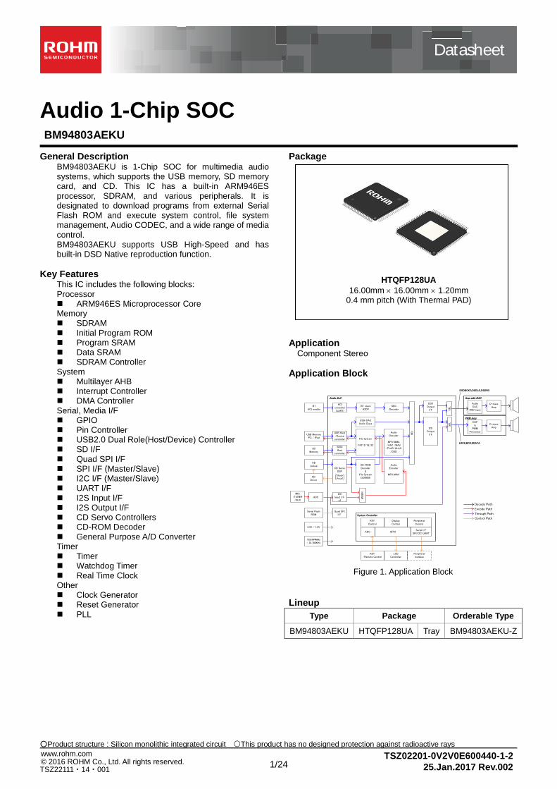
General Description BM94803AEKU is 1-Chip SOC for multimedia audio systems, which supports the USB memory, SD memory card, and CD. This IC has a built-in ARM946ES processor, SDRAM, and various peripherals. It is designated to download programs from external Serial Flash ROM and execute system control, file system management, Audio CODEC, and a wide range of media control. BM94803AEKU supports USB High-Speed and has built-in DSD Native reproduction function.
Key Features This IC includes the following blocks: Processor ARM946ES Microprocessor Core Memory SDRAM Initial Program ROM Program SRAM Data SRAM SDRAM Controller System Multilayer AHB Interrupt Controller DMA Controller Serial, Media I/F GPIO Pin Controller USB2.0 Dual Role(Host/Device) Controller SD I/F Quad SPI I/F SPI I/F (Master/Slave) I2C I/F (Master/Slave) UART I/F I2S Input I/F I2S Output I/F CD Servo Controllers CD-ROM Decoder General Purpose A/D Converter Timer Timer Watchdog Timer Real Time Clock Other Clock Generator Reset Generator PLL
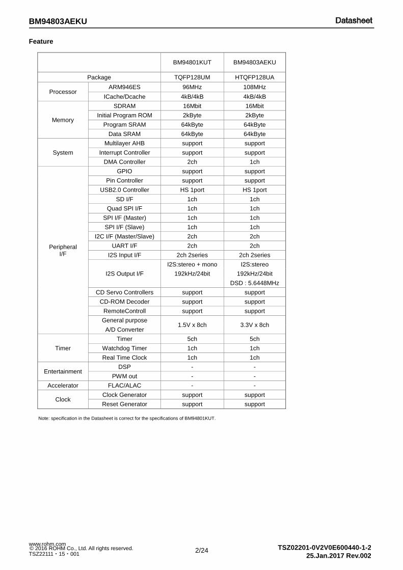
Package
Application Component Stereo
Application Block
Figure 1. Application Block
Lineup
Type Package Orderable Type
BM94803AEKU HTQFP128UA Tray BM94803AEKU-Z
USB MemoryPC / iPod
USB Host/Device
controller
SDMemory
SDIO Host
controller
CDpickup
CD ServoDSP
MIC/TUNER/AUX
I2SInput I/F
x2
File System
FAT12/16/32
Audio Decoder
MP3/WMA/AAC /WAV
/FLAC/ALAC/DSD
CD-ROMDecoder
&File System
ISO9660
SEL
I2SOutput
I/F
DSP&
PWM Processor
PWM Amp
D-classAmp
SEL
AudioEncoder
MP3/WAV
LRCK,BCK,SDATA
MIX
ER
Decode Path
Encode Path
Through Path
USB-DACAudio Class
CDDriver
Control Path
Quad SPII/F
Serial Flash ROM
3.3V / 1.5V
16.9344MHz/ 32.768KHz
KEYControl
DisplayControl
KEY/Remote Control
LCDController
PeripheralControl
ADC GPIOSerial I/F
SPI/I2C/UART
System Controller
Peripheralmodules
DSDOutput
I/F
BTHCI module
HCIcontroller(UART)
BT stackA2DP
SBCDecoder
Audio SoC
SEL
Audio DAC
DSD input
Amp with DAC
D-classAmp
DSDBCKO,DSDLO,DSDRO
ShockProof
ADC
HTQFP128UA
16.00mm 16.00mm 1.20mm 0.4 mm pitch (With Thermal PAD)
2/24
BM94803AEKU
TSZ02201-0V2V0E600440-1-2
25.Jan.2017 Rev.002
© 2016 ROHM Co., Ltd. All rights reserved. www.rohm.com
TSZ22111・15・001
Feature
BM94801KUT BM94803AEKU
Package TQFP128UM HTQFP128UA
Processor ARM946ES 96MHz 108MHz
ICache/Dcache 4kB/4kB 4kB/4kB
Memory
SDRAM 16Mbit 16Mbit
Initial Program ROM 2kByte 2kByte
Program SRAM 64kByte 64kByte
Data SRAM 64kByte 64kByte
System
Multilayer AHB support support
Interrupt Controller support support
DMA Controller 2ch 1ch
Peripheral I/F
GPIO support support
Pin Controller support support
USB2.0 Controller HS 1port HS 1port
SD I/F 1ch 1ch
Quad SPI I/F 1ch 1ch
SPI I/F (Master) 1ch 1ch
SPI I/F (Slave) 1ch 1ch
I2C I/F (Master/Slave) 2ch 2ch
UART I/F 2ch 2ch
I2S Input I/F 2ch 2series 2ch 2series
I2S Output I/F
I2S:stereo + mono I2S:stereo
192kHz/24bit 192kHz/24bit
DSD : 5.6448MHz
CD Servo Controllers support support
CD-ROM Decoder support support
RemoteControll support support
General purpose 1.5V x 8ch 3.3V x 8ch
A/D Converter
Timer
Timer 5ch 5ch
Watchdog Timer 1ch 1ch
Real Time Clock 1ch 1ch
Entertainment DSP - -
PWM out - -
Accelerator FLAC/ALAC - -
Clock Clock Generator support support
Reset Generator support support
Note: specification in the Datasheet is correct for the specifications of BM94801KUT.
3/24
BM94803AEKU
TSZ02201-0V2V0E600440-1-2
25.Jan.2017 Rev.002
© 2016 ROHM Co., Ltd. All rights reserved. www.rohm.com
TSZ22111・15・001
Feature – continued ARM946ES Microprocessor Core 32Bit RISC Processor Operating Frequency: 108MHz 8kByte Cache
Data Cache 4kByte Instruction Cache 4kByte
SDRAM 16Mbit SDRAM with built-in MSM56V16160N from LAPIS Semiconductor 2Bank x 524,288-word x 16Bit Initial Program ROM ITCM ROM Size: 2kByte (512Word x 32Bit) boot program No-wait access REMAP Remapping can be implemented by writing to internal registers. SHADOW SRAM RAM Size: 512Byte (128-Word x 32-Bit) No-wait access Program SRAM ITCM RAM Size: 64kByte (16,384-Word x 32-Bit) No-wait access Data SRAM DTCM RAM Size: 64kByte (16,384-Word x 32-Bit) No-wait access SDRAM Controller Supports SDRAM Supports 11Bit row address, 8-bit column address, and 1-bit bank address to SDRAM AMBA 32Bit Data Bus Arbitrates ARM and DMA access with an arbiter Interrupt Controller 23 IRQ Interrupt Lines 1 FIQ Interrupt Line Allows programmable setting of interrupt priority levels Allows setting of 16 vector addresses DMA Controller Supports 1 Channel Channel FIFO Depth Up to 16 Bytes Allows programmable setting of transfer data width in the range of 1Byte to 4Bytes Allows programmable setting of channel priority levels Maximum Block Length Up to 4,095 Words Includes 12 handshake interfaces available for assignment to channels with software Supports multiblock transfers Connects the master board to system bus GPIO GPIO0(32 pins), GPIO1(32 pins), GPIO2(13pins)
4 of 17 pins assigned GPIO2 are not available because of analog pin. (See P9 Pin Description) Supports a maximum of 77 I/O pins (including 13 GPIO pins for exclusive use) Supports the interrupt function Supports external level-sensitive interrupt
4/24
BM94803AEKU
TSZ02201-0V2V0E600440-1-2
25.Jan.2017 Rev.002
© 2016 ROHM Co., Ltd. All rights reserved. www.rohm.com
TSZ22111・15・001
Feature – continued Pin Controller Controls connection settings between pins and blocks USB2.0 Dual Role (Host/Device) controller USB 2.0 conformance Bit rate: High-Speed (480Mbps)/Full-Speed (12Mbps) Configurable for up to five transmit endpoint FIFOs and four receive endpoint FIFOs (including endpoint 0) Each endpoint FIFO supports bulk transfer, interrupt transfer, and isochronous transfer. 4096-Byte RAM for Endpoint FIFO SD I/F Supports SDHC, and SD cards Provide access to SD card in SD Bus mode Allows control from the AMBA-AHB Bus Includes 512 Byte data transmit/receive FIFOs Quad SPI I/F Supports quad serial flash ROM Supports serial flash ROM address up to 24 bits Allows the setting of control registers from the AMBA-AHB bus Allows direct access from the memory map of the AMBA-AHB bus to serial flash ROM Includes 32 byte transmit/receive FIFOs SSI Master FIFO Depth Up to 16 Words and FIFO Data Width Up to 16Bits Selectable Data Size from 4 Bits to 16 Bits Serial protocol supports SPI from Motorola Includes DMA handshake interface SSI Slave FIFO Depth Up to 16 Words and FIFO Data Width Up to 16 Bits Selectable Data Size from 4 Bits to 16 Bits Serial protocol supports SPI from Motorola Includes DMA handshake interface I2C I/F (Master/Slave) 2 Ch I2C Serial Interface Supports two speed modes Standard mode (100Kb/s) Fast mode (400Kb/s) Supports I2C Master and Slave operation Allows 7 and 10 bit address generation Has built-in 32 stage transmit and receive FIFOs Includes DMA handshake interface UART I/F IS16550-Based Allows various baud rate settings with software (up to 6Mbps) No Support for IrDA FIFO Depth Up to 32 Words and FIFO Data Width Up to 8 Bits Incorporates a function to invert output Includes DMA handshake interface
5/24
BM94803AEKU
TSZ02201-0V2V0E600440-1-2
25.Jan.2017 Rev.002
© 2016 ROHM Co., Ltd. All rights reserved. www.rohm.com
TSZ22111・15・001
Feature – continued I2S Input I/F Two Lines of 2-Ch Digital Audio Input I2S, EIAJ format 16-Bit Data Selectable Bit Clock from 32fs, 48fs, and 64fs Selectable Input Sample Rate from 32kHz, 44.1kHz, and 48kHz One Line of Internal Input from the CD Servo Controller Maximum Input Rate Up to 4x Supports detection of CD-DA link Supports detection of CD-ROM sync Supports CD-ROM data descrambling Acquires Sub-Q data Acquires CD-Text data Built-in DMA 2ch Supports I2S Input at CD Play I2S Output I/F 2-Ch Digital Audio Output x 1 ( 2ch from Decoder) I2S, EIAJ format Selectable PCM Output Sample Rate from 32k, 44.1k, 48k, 88.2k, 96k,176.4k,192kHz Selectable PCM Data Width from 16 and 24 bits 64 fs PCM Bit Clock Supports pitch control (x0.5 - x2.0, 25step) Selectable DSD Output Sample Rate from DSD 2.8224MHz, 5.6448MHz CD servo controller Supports rotation speed of CD up to 4x Built-in Preservo-Amplifier with Power Save Mode, which supports Playback of CD-RW Allows independent offset adjustment of AC, BD, E, and F amplifiers Built-in Auto-Tracking and Focus Adjustment Function Built-in PLL and CLV with a Wide Lock Range Built-in Asymmetry Correction Function CD-ROM Decoder Supports Mode1, Mode2 form1, Mode2 form2 Supports ECC, EDC Built-in DMA General Purpose A/D Converter 10-Bit SAR ADC, 8 Ch ADC Analog Input Voltage range: VDD_ADC x10% to VDD_ADC x 90% Maximum A/D Conversion frequency Ch=88.2ksps Timer Supports five independent programmable timer functions Each timer supports time width up to 32 bits Each timer supports independent interrupt signal Watchdog Timer Composed of a counter having a set cycle to monitor the occurrence of timeout event Counter Width Up to 32 Bits The counter counts down from the set value and sets timeout occurrence when it reaches zero Realtime clock 32 Bit Programmable Timer Supports interrupt signals External 32.768 kHz Crystal Oscillator
6/24
BM94803AEKU
TSZ02201-0V2V0E600440-1-2
25.Jan.2017 Rev.002
© 2016 ROHM Co., Ltd. All rights reserved. www.rohm.com
TSZ22111・15・001
Feature – continued Remote Controller Receiver (RCR) Converts infrared remote control signal to code Compatible with the signal format of the Association for Electric Home Appliances Supports Sony format Enables to setup permissible value of input signal cycle to adjust the Duty deviation of input signal Clock Generator Supplies clocks to individual internal blocks Allows on/off control of clocks to individual blocks Generates master audio clocks At the normal operation, supports three modes (High-Speed mode, Middle Speed mode, Low-Speed mode) Supports Standby Mode Reset Generator Generates a pulse to be supplied to individual blocks PLL Generates 216MHz / 240MHz clock used to generate system clocks Generates 135.4752 MHz and 147.456 MHz clocks used to generate audio clocks Power Supply Voltage I/O Power Supply Voltage : 3.3V(3.0V to 3.6V) Analog Power Supply Voltage: 3.3V(3.0V to 3.6V)
(Used for SDRAM, CD servo, USB, and ADC) Digital Core Power Supply Voltage : 1.5V(1.45V to 1.65V)
(Used for Digital Core)
7/24
BM94803AEKU
TSZ02201-0V2V0E600440-1-2
25.Jan.2017 Rev.002
© 2016 ROHM Co., Ltd. All rights reserved. www.rohm.com
TSZ22111・15・001
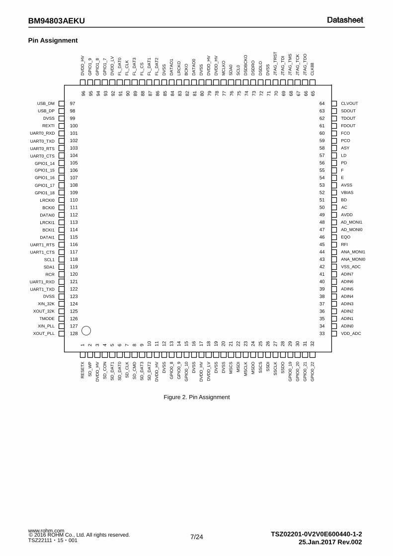
Pin Assignment
Figure 2. Pin Assignment
RE
SE
TX
SD
_W
P
DV
DD
_H
V
SD
_D
AT
0
SD
_C
LK
SD
_C
MD
SD
_D
AT
3
DV
DD
_H
V
GP
IO0
_9
GP
IO0
_1
0
DV
DD
_L
V
DV
SS
DV
DD
_H
V
DV
SS
DV
SS
DV
SS
GP
IO1
_8
DV
DD
_L
V
FL_
CS
DV
SS
DA
TA
O1
FL_
DA
T2
DV
SS
DV
DD
_H
V
DA
TA
O0
FL_
DA
T1
FL_
DA
T3
FL_
CL
K
MC
LK
O
DV
DD
_H
V
BC
KO
FL_
DA
T0
XOUT_32K
LRCKI1
DATAI0
BCKI0
BCKI1
LRCKI0
DATAI1
XIN_32K
DVSS
UART1_RTS
XIN_PLL
RCR
TMODE
XOUT_PLL
LR
CK
O
ADIN0
ADIN2
ADIN3
ADIN4
ADIN5
ADIN6
ADIN7
AC
EQO
AD_MONI0
VBIAS
ADIN1
ANA_MONI1
BD
SD
_D
AT
1
RFI
VDD_ADC
AVDD
SD
_D
AT
2
GP
IO0
_8
UART1_TXD
AD_MONI1
GP
IO1
_9
DV
DD
_H
V
GP
IO1
_7
UART1_CTS
SDA1
SCL1
SD
_C
ON
UART1_RXD
ANA_MONI0
VSS_ADC
123
122
121
120
119
118
117
116
115
114
113
112
111
128
127
126
125
124
96
95
94
93
92
91
90
89
88
87
86
85
84
83
82
81
80
79
78
40
41
42
43
44
45
46
47
48
49
50
51
52
33
34
35
36
37
38
39
1 2 3 4 5 6 7 8 9 10
11
12
13
14
15
16
17
18
19
MS
CS
MS
DI
SS
CS
SS
DI
SS
CL
K
SS
DO
GP
IO0
_2
0
GP
IO0
_2
1
MS
DO
GP
IO0
_1
9
GP
IO0
_2
2
MS
CL
K
20
21
22
23
24
25
26
27
28
29
30
31
32
SC
L0
DS
DR
O
JT
AG
_T
DI
JT
AG
_T
DO
CL
K8
8
JT
AG
_T
CK
JT
AG
_T
MS
JT
AG
_T
RS
T
DV
SS
DS
DL
O
SD
A0
DS
DB
CK
O
77
76
75
74
73
72
71
70
69
68
67
66
AVSS
F
PD
LD
ASY
PCO
FCO
E
SDOUT
CLVOUT
TDOUT
FDOUT
59
60
61
62
63
64
53
54
55
56
57
58
GPIO1_15
GPIO1_14
UART0_CTS
GPIO1_18
REXTI
GPIO1_16
UART0_RTS
USB_DM
DVSS
USB_DP
UART0_TXD
104
103
102
101
100
99
110
109
108
107
106
105
65
98
97
GPIO1_17
UART0_RXD
8/24
BM94803AEKU
TSZ02201-0V2V0E600440-1-2
25.Jan.2017 Rev.002
© 2016 ROHM Co., Ltd. All rights reserved. www.rohm.com
TSZ22111・15・001
Pin Description No Block Pin Name GPIO I/O Function
1 RESET RESETX I H: Release RESET, L: RESET
2 SD SD_WP GPIO0[0] I/O SD Card I/F WP Detect
3 POWER DVDD_HV - 3.3V Power Supply
4 SD SD_CON GPIO0[1] I/O SD Card I/F Connection Detect
5 SD SD_DAT1 GPIO0[2] I/O SD Card I/F Data I/O (1)
6 SD SD_DAT0 GPIO0[3] I/O SD Card I/F Data I/O (0)
7 SD SD_CLK GPIO0[4] I/O SD Card I/F Clock Output
8 SD SD_CMD GPIO0[5] I/O SD Card I/F Command Output
9 SD SD_DAT3 GPIO0[6] I/O SD Card I/F Data I/O (3)
10 SD SD_DAT2 GPIO0[7] I/O SD Card I/F Data I/O (2)
11 POWER DVDD_HV - 3.3V Power Supply
12 POWER DVSS - GND
13 GPIO GPIO0_8 GPIO0[8] I/O GPIO for exclusive use
14 GPIO GPIO0_9 GPIO0[9] I/O GPIO pin. When CD is used, this pin is TRAY OPEN/CLOSE detect pin of CD mechanical tray.
15 GPIO GPIO0_10 GPIO0[10] I/O GPIO for exclusive use
16 POWER DVSS - GND
17 POWER DVDD_HV - 3.3V Power Supply
18 POWER DVDD_LV - 1.5V Power Supply
19 POWER DVSS - GND
20 POWER DVSS - GND
21 MSIO MSCS GPIO0[11] I/O SIO Master Chip Select Output
22 MSIO MSDI GPIO0[12] I/O SIO Master Data Input
23 MSIO MSCLK GPIO0[13] I/O SIO Master Clock Output
24 MSIO MSDO GPIO0[14] I/O SIO Master Data Output
25 SSIO SSCS GPIO0[15] I/O SIO Slave Chip Select Input
26 SSIO SSDI GPIO0[16] I/O SIO Slave Data Input
27 SSIO SSCLK GPIO0[17] I/O SIO Slave Clock Input
28 SSIO SSDO GPIO0[18] I/O SIO Slave Data Output
29 GPIO GPIO0_19 GPIO0[19] I/O GPIO for exclusive use
30 GPIO GPIO0_20 GPIO0[20] I/O GPIO for exclusive use
31 GPIO GPIO0_21 GPIO0[21] I/O GPIO pin. When CD is used, this pin is INNER_SW detect pin.
32 GPIO GPIO0_22 GPIO0[22] I/O GPIO for exclusive use
33 POWER VDD_ADC - 3.3V ADC Power Supply
34 ADC ADIN0 GPIO2[0] I AD input CH0 or GPIO
35 ADC ADIN1 GPIO2[1] I AD input CH1 or GPIO
36 ADC ADIN2 GPIO2[2] I AD input CH2 or GPIO
37 ADC ADIN3 GPIO2[3] I AD input CH3 or GPIO
38 ADC ADIN4 GPIO2[4] I AD input CH4 or GPIO
39 ADC ADIN5 GPIO2[5] I AD input CH5 or GPIO
40 ADC ADIN6 GPIO2[6] I AD input CH6 or GPIO
41 ADC ADIN7 GPIO2[7] I AD input CH7 or GPIO
42 POWER VSS_ADC - ADC GND
43 CDDSP ANA_MONI0 GPIO2[8] I/O Input & Analog Monitor Output or GPIO
44 CDDSP ANA_MONI1 GPIO2[9] I/O Input & Analog Monitor Output or GPIO
45 CDDSP RFI I RF Output Capacitance Coupling Re-Input
46 CDDSP EQO O Output RF Equalizer
47 CDDSP AD_MONI0 GPIO2[10] I/O Input & Monitor Signal Output or GPIO
48 CDDSP AD_MONI1 GPIO2[11] I/O Input & Monitor Signal Output or GPIO
49 POWER AVDD - 3.3V CD RF Power Supply
50 CDDSP AC I A + C Voltage Input
51 CDDSP BD I B + D Voltage Input
52 CDDSP VBIAS O VBIAS Output
53 POWER AVSS - CD RF GND
54 CDDSP E I E Voltage Input
55 CDDSP F I F Voltage Input
56 CDDSP PD I APC Photo Detector Input
57 CDDSP LD O APC Laser Drive Output
9/24
BM94803AEKU
TSZ02201-0V2V0E600440-1-2
25.Jan.2017 Rev.002
© 2016 ROHM Co., Ltd. All rights reserved. www.rohm.com
TSZ22111・15・001
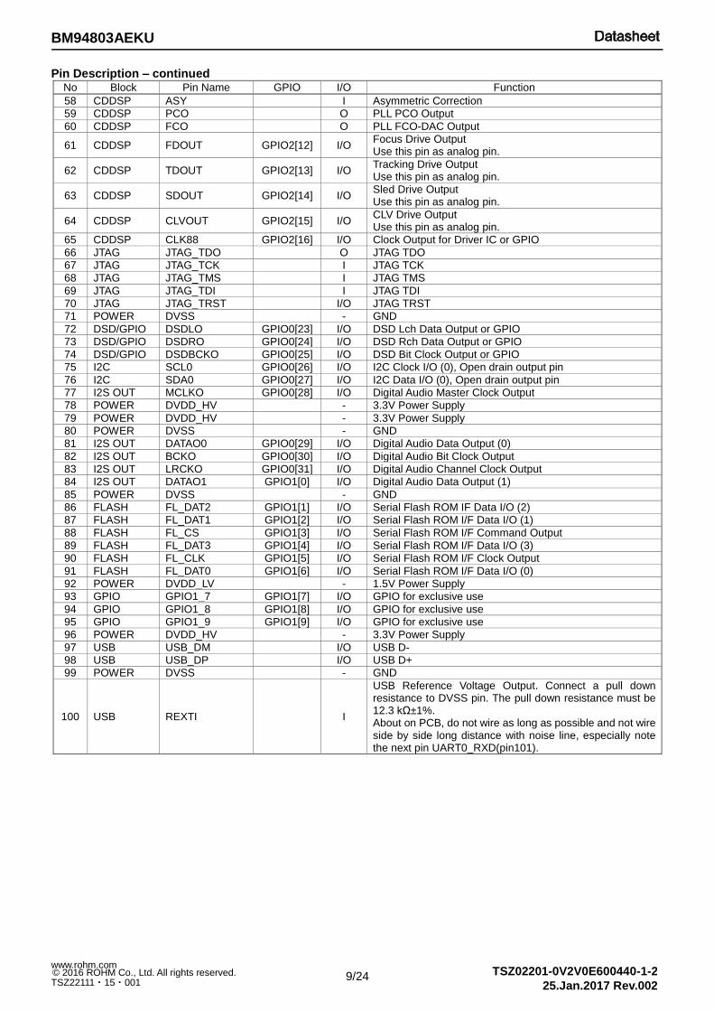
Pin Description – continued No Block Pin Name GPIO I/O Function
58 CDDSP ASY I Asymmetric Correction
59 CDDSP PCO O PLL PCO Output
60 CDDSP FCO O PLL FCO-DAC Output
61 CDDSP FDOUT GPIO2[12] I/O Focus Drive Output Use this pin as analog pin.
62 CDDSP TDOUT GPIO2[13] I/O Tracking Drive Output Use this pin as analog pin.
63 CDDSP SDOUT GPIO2[14] I/O Sled Drive Output Use this pin as analog pin.
64 CDDSP CLVOUT GPIO2[15] I/O CLV Drive Output Use this pin as analog pin.
65 CDDSP CLK88 GPIO2[16] I/O Clock Output for Driver IC or GPIO
66 JTAG JTAG_TDO O JTAG TDO
67 JTAG JTAG_TCK I JTAG TCK
68 JTAG JTAG_TMS I JTAG TMS
69 JTAG JTAG_TDI I JTAG TDI
70 JTAG JTAG_TRST I/O JTAG TRST
71 POWER DVSS - GND
72 DSD/GPIO DSDLO GPIO0[23] I/O DSD Lch Data Output or GPIO
73 DSD/GPIO DSDRO GPIO0[24] I/O DSD Rch Data Output or GPIO
74 DSD/GPIO DSDBCKO GPIO0[25] I/O DSD Bit Clock Output or GPIO
75 I2C SCL0 GPIO0[26] I/O I2C Clock I/O (0), Open drain output pin
76 I2C SDA0 GPIO0[27] I/O I2C Data I/O (0), Open drain output pin
77 I2S OUT MCLKO GPIO0[28] I/O Digital Audio Master Clock Output
78 POWER DVDD_HV - 3.3V Power Supply
79 POWER DVDD_HV - 3.3V Power Supply
80 POWER DVSS - GND
81 I2S OUT DATAO0 GPIO0[29] I/O Digital Audio Data Output (0)
82 I2S OUT BCKO GPIO0[30] I/O Digital Audio Bit Clock Output
83 I2S OUT LRCKO GPIO0[31] I/O Digital Audio Channel Clock Output
84 I2S OUT DATAO1 GPIO1[0] I/O Digital Audio Data Output (1)
85 POWER DVSS - GND
86 FLASH FL_DAT2 GPIO1[1] I/O Serial Flash ROM IF Data I/O (2)
87 FLASH FL_DAT1 GPIO1[2] I/O Serial Flash ROM I/F Data I/O (1)
88 FLASH FL_CS GPIO1[3] I/O Serial Flash ROM I/F Command Output
89 FLASH FL_DAT3 GPIO1[4] I/O Serial Flash ROM I/F Data I/O (3)
90 FLASH FL_CLK GPIO1[5] I/O Serial Flash ROM I/F Clock Output
91 FLASH FL_DAT0 GPIO1[6] I/O Serial Flash ROM I/F Data I/O (0)
92 POWER DVDD_LV - 1.5V Power Supply
93 GPIO GPIO1_7 GPIO1[7] I/O GPIO for exclusive use
94 GPIO GPIO1_8 GPIO1[8] I/O GPIO for exclusive use
95 GPIO GPIO1_9 GPIO1[9] I/O GPIO for exclusive use
96 POWER DVDD_HV - 3.3V Power Supply
97 USB USB_DM I/O USB D-
98 USB USB_DP I/O USB D+
99 POWER DVSS - GND
100 USB REXTI I
USB Reference Voltage Output. Connect a pull down resistance to DVSS pin. The pull down resistance must be 12.3 kΩ±1%. About on PCB, do not wire as long as possible and not wire side by side long distance with noise line, especially note the next pin UART0_RXD(pin101).
10/24
BM94803AEKU
TSZ02201-0V2V0E600440-1-2
25.Jan.2017 Rev.002
© 2016 ROHM Co., Ltd. All rights reserved. www.rohm.com
TSZ22111・15・001
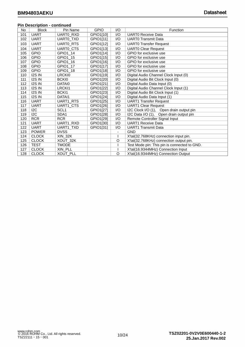
Pin Description - continued No Block Pin Name GPIO I/O Function
101 UART UART0_RXD GPIO1[10] I/O UART0 Receive Data
102 UART UART0_TXD GPIO1[11] I/O UART0 Transmit Data
103 UART UART0_RTS GPIO1[12] I/O UART0 Transfer Request
104 UART UART0_CTS GPIO1[13] I/O UART0 Clear Request
105 GPIO GPIO1_14 GPIO1[14] I/O GPIO for exclusive use
106 GPIO GPIO1_15 GPIO1[15] I/O GPIO for exclusive use
107 GPIO GPIO1_16 GPIO1[16] I/O GPIO for exclusive use
108 GPIO GPIO1_17 GPIO1[17] I/O GPIO for exclusive use
109 GPIO GPIO1_18 GPIO1[18] I/O GPIO for exclusive use
110 I2S IN LRCKI0 GPIO1[19] I/O Digital Audio Channel Clock Input (0)
111 I2S IN BCKI0 GPIO1[20] I/O Digital Audio Bit Clock Input (0)
112 I2S IN DATAI0 GPIO1[21] I/O Digital Audio Data Input (0)
113 I2S IN LRCKI1 GPIO1[22] I/O Digital Audio Channel Clock Input (1)
114 I2S IN BCKI1 GPIO1[23] I/O Digital Audio Bit Clock Input (1)
115 I2S IN DATAI1 GPIO1[24] I/O Digital Audio Data Input (1)
116 UART UART1_RTS GPIO1[25] I/O UART1 Transfer Request
117 UART UART1_CTS GPIO1[26] I/O UART1 Clear Request
118 I2C SCL1 GPIO1[27] I/O I2C Clock I/O (1), Open drain output pin
119 I2C SDA1 GPIO1[28] I/O I2C Data I/O (1), Open drain output pin
120 RCR RCR GPIO1[29] I/O Remote Controller Signal Input
121 UART UART1_RXD GPIO1[30] I/O UART1 Receive Data
122 UART UART1_TXD GPIO1[31] I/O UART1 Transmit Data
123 POWER DVSS - GND
124 CLOCK XIN_32K I X'tal(32.768KHz) connection input pin.
125 CLOCK XOUT_32K O X'tal(32.768KHz) connection output pin.
126 TEST TMODE I Test Mode pin: This pin is connected to GND.
127 CLOCK XIN_PLL I X'tal(16.9344MHz) Connection Input
128 CLOCK XOUT_PLL O X'tal(16.9344MHz) Connection Output
11/24
BM94803AEKU
TSZ02201-0V2V0E600440-1-2
25.Jan.2017 Rev.002
© 2016 ROHM Co., Ltd. All rights reserved. www.rohm.com
TSZ22111・15・001
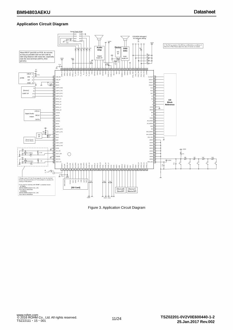
Application Circuit Diagram
Figure 3. Application Circuit Diagram
Write
pro
tect
DA
T1
DA
T0
CL
K
CD
M
DA
T3
DA
T2
[SD Card]
0.1µ
Co
nn
ect
Device
I2C
I/F
CD
Block
Reference
Audio
Amp
Digital
Audio I/F
SIO0
SCLK
SIO3
VCC
GND
SIO2
SIO1
CS#
Serial Flash ROM
0.1µ
22 22 22 22 22 22
VDDH
LRCLK
BCLK
DATA
Digital Audio
output
10p
0
1M
32.768kHz
16.9344MHz
0.1µ 0.1µ
[Device0]SlaveSPI
0.1μ
0.1μ
680 1.2K 2.2K 6.8K
2.7k
0.1µ
270
10p
10p
10p
[Device]
UART I/F
CTS
RTS
RX
TX
Remote Control Receiver Module
0.1µVDDH
VDDH VDDH VDDL
VDDH
VDDH
VDDH
0.1µ
VDDL
[Device1]MasterSPI
DSD
DAC
DSD
Audio I/F
VBUS 1
DM 2
DP 3
GND 4
5V
0.1µ
0.1µ
VDDH
[USB]
12.3k
1 2 3 4 5 6 7 8 9 10
11
12
13
14
15
16
17
18
19
20
21
22
23
24
25
26
27
28
29
30
31
32
40
41
42
43
44
45
46
47
48
49
50
51
52
33
34
35
36
37
38
39
59
60
61
62
63
64
53
54
55
56
57
58
96
95
94
93
92
91
90
89
88
87
86
85
84
83
82
81
80
79
78
77
76
75
74
73
72
71
70
69
68
67
66
65
123
122
121
120
119
118
117
116
115
114
113
112
111
128
127
126
125
124
104
103
102
101
100
99
110
109
108
107
106
105
98
97
GP
IO0_
21
GP
IO0_
22
RE
SE
TX
SD
_W
P
DV
DD
_H
V
SD
_D
AT
0
SD
_C
LK
SD
_C
MD
SD
_D
AT
3
DV
DD
_H
V
GP
IO0
_9
GP
IO0
_1
0
DV
DD
_L
V
DV
SS
DV
DD
_H
V
DV
SS
DV
SS
DV
SS
SD
_D
AT
1
SD
_D
AT
2
GP
IO0
_8
SD
_C
ON
MS
CS
MS
DI
SS
CS
SS
DI
SS
CL
K
SS
DO
GP
IO0
_2
0
MS
DO
GP
IO0
_1
9
MS
CL
K
GP
IO1_
8
DV
DD
_L
V
FL
_C
S
DV
SS
DA
TA
O1
FL_
DA
T2
DV
SS
DV
DD
_H
V
DA
TA
O0
FL_
DA
T1
FL_
DA
T3
FL
_C
LK
MC
LK
O
DV
DD
_H
V
BC
KO
FL_
DA
T0
LR
CK
O
GP
IO1_
9
DV
DD
_H
V
GP
IO1_
7
SC
L0
DS
DR
O
JT
AG
_T
DI
JT
AG
_T
DO
CL
K8
8
JT
AG
_T
CK
JT
AG
_T
MS
JT
AG
_T
RS
T
DV
SS
DS
DL
O
SD
A0
DS
DB
CK
O
ANA_MONI1
ADIN0
ADIN2
ADIN3
ADIN4
ADIN5
ADIN6
ADIN7
AC
EQO
AD_MONI0
VBIAS
ADIN1
BD
RFI
VDD_ADC
AVDD
AD_MONI1
ANA_MONI0
VSS_ADC
AVSS
F
PD
LD
ASY
PCO
FCO
E
SDOUT
CLVOUT
TDOUT
FDOUT
UART0_TXD
XOUT_32K
LRCKI1
DATAI0
BCKI0
BCKI1
LRCKI0
DATAI1
XIN_32K
DVSS
UART1_RTS
XIN_PLL
RCR
TMODE
XOUT_PLL
UART1_TXD
UART1_CTS
SDA1
SCL1
UART1_RXD
GPIO1_15
GPIO1_14
UART0_CTS
GPIO1_18
REXTI
GPIO1_16
UART0_RTS
USB_DM
DVSS
USB_DP
GPIO1_17
UART0_RXD
I2C
I/F
H
L
About REXT (pin100) on PCB, do not wire
as long as possible and not wire side by
side long distance with noise line, especially
note the next terminal UART0_RXD
(pin101).
VDDH
ICE(ARM debugger)
for software debug
10k
10k
10k
10k
33
4.7M
10k
(*)10k
(*)
10k
(*)
10k
(*)
*. The Pull-up resistor of the I2C bus is affected by a condition of Slave IC or PCB. Please adjust the value of resistor as needed.
* Design route of X’tal, IC and capacitor to be the shortest because the characteristic of X’tal oscillation is sensitive for routing of PCB pattern.
X’tal using for matching with ROHM’s evaluation board- 32.768kHz NIHON DEMPA KOGYO CO., LTD. Parts Name:NX3215SA- 16.9344MHz NIHON DEMPA KOGYO CO., LTD. Parts Name:NX3225GA
12/24
BM94803AEKU
TSZ02201-0V2V0E600440-1-2
25.Jan.2017 Rev.002
© 2016 ROHM Co., Ltd. All rights reserved. www.rohm.com
TSZ22111・15・001
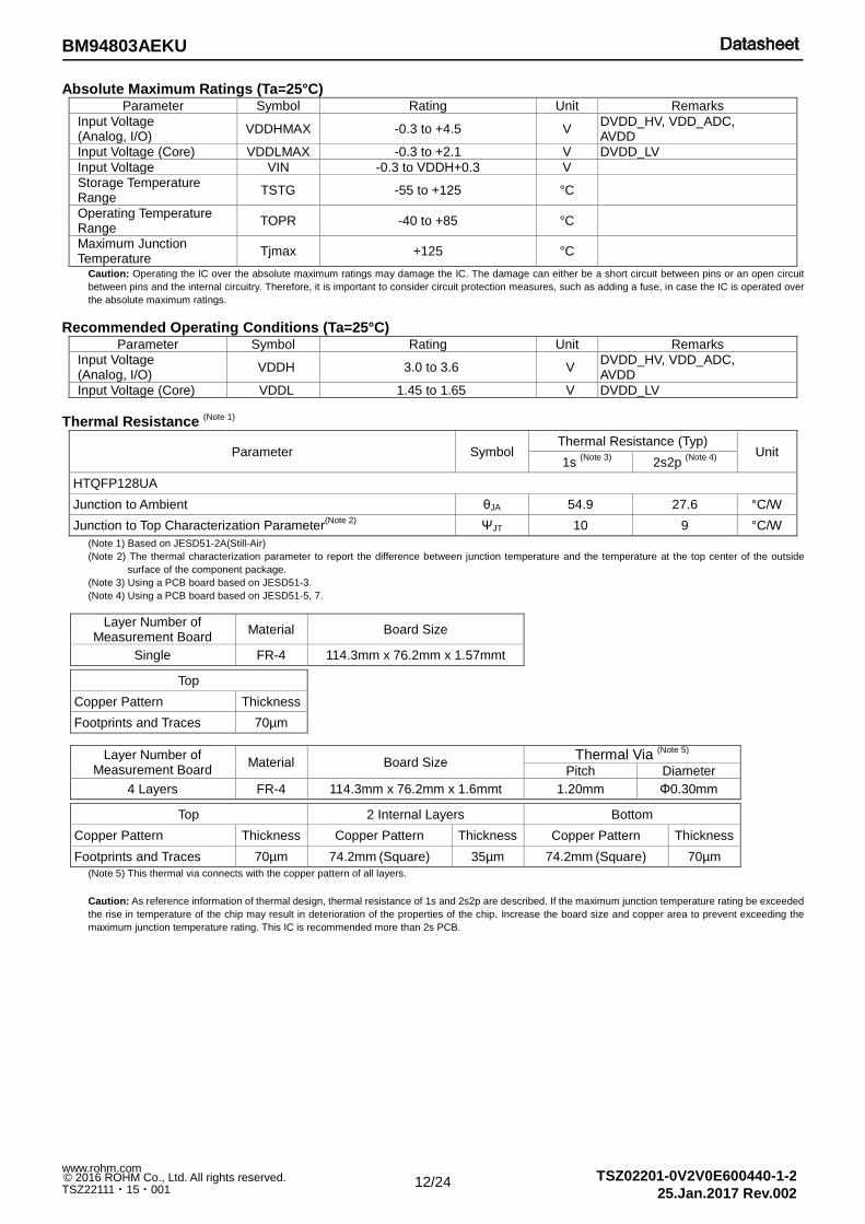
Absolute Maximum Ratings (Ta=25°C) Parameter Symbol Rating Unit Remarks
Input Voltage (Analog, I/O)
VDDHMAX -0.3 to +4.5 V DVDD_HV, VDD_ADC, AVDD
Input Voltage (Core) VDDLMAX -0.3 to +2.1 V DVDD_LV
Input Voltage VIN -0.3 to VDDH+0.3 V
Storage Temperature Range
TSTG -55 to +125 °C
Operating Temperature Range
TOPR -40 to +85 °C
Maximum Junction Temperature
Tjmax +125 °C
Caution: Operating the IC over the absolute maximum ratings may damage the IC. The damage can either be a short circuit between pins or an open circuit
between pins and the internal circuitry. Therefore, it is important to consider circuit protection measures, such as adding a fuse, in case the IC is operated over
the absolute maximum ratings.
Recommended Operating Conditions (Ta=25°C) Parameter Symbol Rating Unit Remarks
Input Voltage (Analog, I/O)
VDDH 3.0 to 3.6 V DVDD_HV, VDD_ADC, AVDD
Input Voltage (Core) VDDL 1.45 to 1.65 V DVDD_LV
Thermal Resistance (Note 1)
Parameter Symbol Thermal Resistance (Typ)
Unit 1s
(Note 3) 2s2p
(Note 4)
HTQFP128UA
Junction to Ambient θJA 54.9 27.6 °C/W
Junction to Top Characterization Parameter(Note 2)
ΨJT 10 9 °C/W
(Note 1) Based on JESD51-2A(Still-Air)
(Note 2) The thermal characterization parameter to report the difference between junction temperature and the temperature at the top center of the outside
surface of the component package.
(Note 3) Using a PCB board based on JESD51-3.
(Note 4) Using a PCB board based on JESD51-5, 7.
Layer Number of Measurement Board
Material Board Size
Single FR-4 114.3mm x 76.2mm x 1.57mmt
Top
Copper Pattern Thickness
Footprints and Traces 70µm
Layer Number of Measurement Board
Material Board Size Thermal Via (Note 5)
Pitch Diameter
4 Layers FR-4 114.3mm x 76.2mm x 1.6mmt 1.20mm Φ0.30mm
Top 2 Internal Layers Bottom
Copper Pattern Thickness Copper Pattern Thickness Copper Pattern Thickness
Footprints and Traces 70µm 74.2mm (Square) 35µm 74.2mm
(Square) 70µm
(Note 5) This thermal via connects with the copper pattern of all layers.
Caution: As reference information of thermal design, thermal resistance of 1s and 2s2p are described. If the maximum junction temperature rating be exceeded
the rise in temperature of the chip may result in deterioration of the properties of the chip. Increase the board size and copper area to prevent exceeding the
maximum junction temperature rating. This IC is recommended more than 2s PCB.
13/24
BM94803AEKU
TSZ02201-0V2V0E600440-1-2
25.Jan.2017 Rev.002
© 2016 ROHM Co., Ltd. All rights reserved. www.rohm.com
TSZ22111・15・001
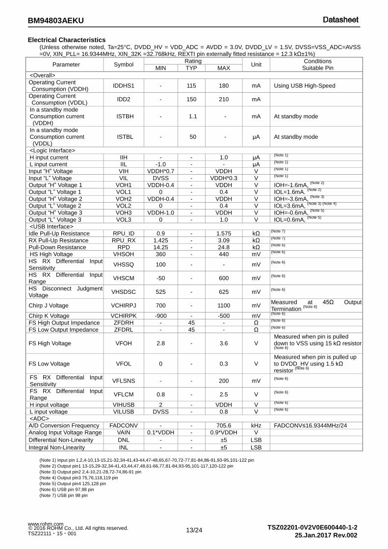
Electrical Characteristics (Unless otherwise noted, Ta=25°C, DVDD_HV = VDD_ADC = AVDD = 3.0V, DVDD_LV = 1.5V, DVSS=VSS_ADC=AVSS =0V, XIN_PLL= 16.9344MHz, XIN_32K =32.768kHz, REXTI pin externally fitted resistance = 12.3 kΩ±1%)
Parameter Symbol Rating
Unit Conditions
Suitable Pin MIN TYP MAX
<Overall>
Operating Current Consumption (VDDH)
IDDHS1 - 115 180 mA Using USB High-Speed
Operating Current Consumption (VDDL)
IDD2 - 150 210 mA
In a standby mode Consumption current (VDDH)
ISTBH - 1.1 - mA At standby mode
In a standby mode Consumption current (VDDL)
ISTBL - 50 - μA At standby mode
<Logic Interface>
H input current IIH - - 1.0 μA (Note 1)
L input current IIL -1.0 - - μA (Note 1)
Input “H” Voltage VIH VDDH*0.7 - VDDH V (Note 1)
Input “L” Voltage VIL DVSS - VDDH*0.3 V (Note 1)
Output “H” Voltage 1 VOH1 VDDH-0.4 - VDDH V IOH=-1.6mA, (Note 2)
Output “L” Voltage 1 VOL1 0 - 0.4 V IOL=1.6mA. (Note 2)
Output “H” Voltage 2 VOH2 VDDH-0.4 - VDDH V IOH=-3.6mA, (Note 3)
Output “L” Voltage 2 VOL2 0 - 0.4 V IOL=3.6mA, (Note 3) (Note 4)
Output “H” Voltage 3 VOH3 VDDH-1.0 - VDDH V IOH=-0.6mA, (Note 5)
Output “L” Voltage 3 VOL3 0 - 1.0 V IOL=0.6mA, (Note 5)
<USB Interface>
Idle Pull-Up Resistance RPU_ID 0.9 - 1.575 kΩ (Note 7)
RX Pull-Up Resistance RPU_RX 1.425 - 3.09 kΩ (Note 7)
Pull-Down Resistance RPD 14.25 - 24.8 kΩ (Note 6)
HS High Voltage VHSOH 360 - 440 mV (Note 6)
HS RX Differential Input Sensitivity
VHSSQ 100 - - mV (Note 6)
HS RX Differential Input Range
VHSCM -50 - 600 mV (Note 6)
HS Disconnect Judgment Voltage
VHSDSC 525 - 625 mV (Note 6)
Chirp J Voltage VCHIRPJ 700 - 1100 mV Measured at 45Ω Output Termination
(Note 6)
Chirp K Voltage VCHIRPK -900 - -500 mV (Note 6)
FS High Output Impedance ZFDRH - 45 - Ω (Note 6)
FS Low Output Impedance ZFDRL - 45 - Ω (Note 6)
FS High Voltage VFOH 2.8 - 3.6 V Measured when pin is pulled down to VSS using 15 kΩ resistor
(Note 6)
FS Low Voltage VFOL 0 - 0.3 V Measured when pin is pulled up to DVDD_HV using 1.5 kΩ resistor
(Note 6)
FS RX Differential Input Sensitivity
VFLSNS - - 200 mV (Note 6)
FS RX Differential Input Range
VFLCM 0.8 - 2.5 V (Note 6)
H input voltage VIHUSB 2 - VDDH V (Note 6)
L input voltage VILUSB DVSS - 0.8 V (Note 6)
<ADC>
A/D Conversion Frequency FADCONV - - 705.6 kHz FADCONV≤16.9344MHz/24
Analog Input Voltage Range VAIN 0.1*VDDH - 0.9*VDDH V
Differential Non-Linearity DNL - - ±5 LSB
Integral Non-Linearity INL - - ±5 LSB
(Note 1) Input pin 1,2,4-10,13-15,21-32,34-41,43-44,47-48,65,67-70,72-77,81-84,86-91,93-95,101-122 pin
(Note 2) Output pin1 13-15,29-32,34-41,43,44,47,48,61-66,77,81-84,93-95,101-117,120-122 pin
(Note 3) Output pin2 2,4-10,21-28,72-74,86-91 pin
(Note 4) Output pin3 75,76,118,119 pin
(Note 5) Output pin4 125,128 pin
(Note 6) USB pin 97,98 pin
(Note 7) USB pin 98 pin
14/24
BM94803AEKU
TSZ02201-0V2V0E600440-1-2
25.Jan.2017 Rev.002
© 2016 ROHM Co., Ltd. All rights reserved. www.rohm.com
TSZ22111・15・001
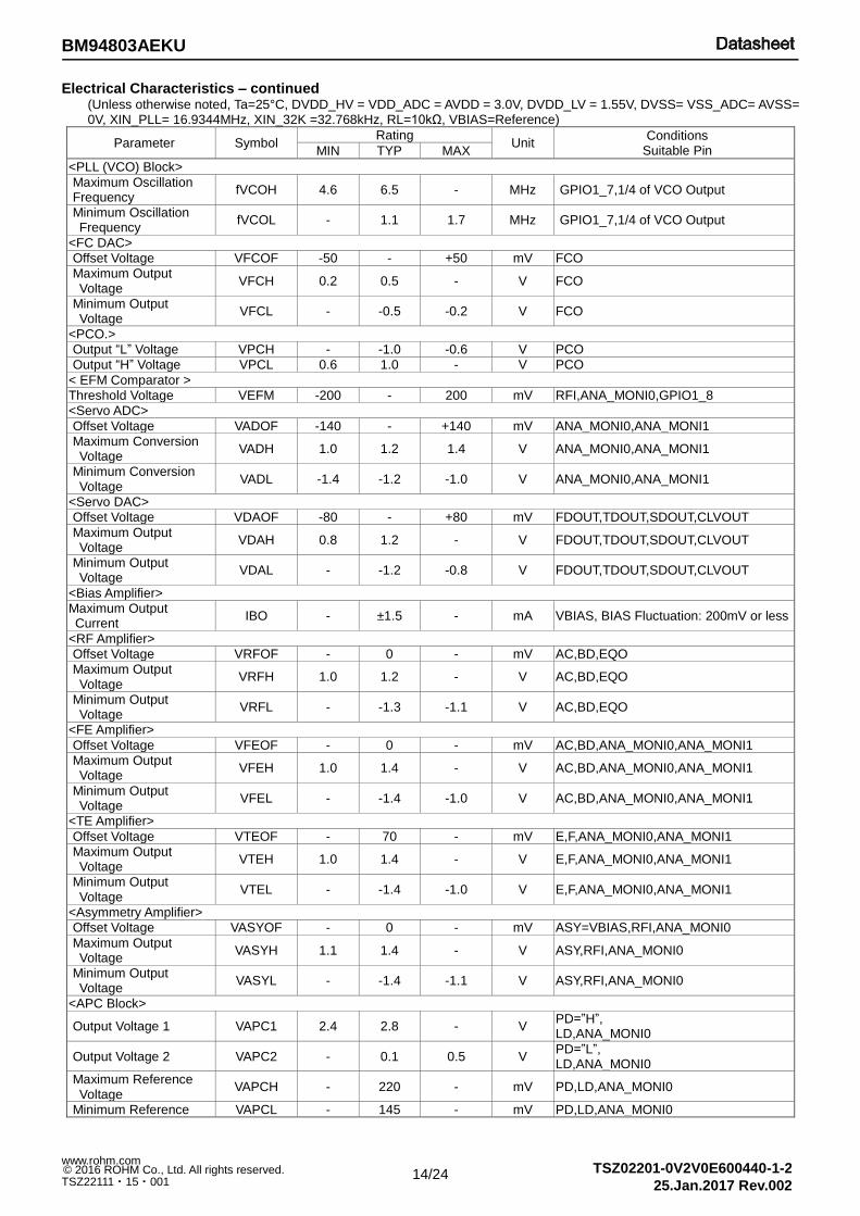
Electrical Characteristics – continued (Unless otherwise noted, Ta=25°C, DVDD_HV = VDD_ADC = AVDD = 3.0V, DVDD_LV = 1.55V, DVSS= VSS_ADC= AVSS= 0V, XIN_PLL= 16.9344MHz, XIN_32K =32.768kHz, RL=10kΩ, VBIAS=Reference)
Parameter Symbol Rating
Unit Conditions
Suitable Pin MIN TYP MAX
<PLL (VCO) Block>
Maximum Oscillation Frequency
fVCOH 4.6 6.5 - MHz GPIO1_7,1/4 of VCO Output
Minimum Oscillation Frequency
fVCOL - 1.1 1.7 MHz GPIO1_7,1/4 of VCO Output
<FC DAC>
Offset Voltage VFCOF -50 - +50 mV FCO
Maximum Output Voltage
VFCH 0.2 0.5 - V FCO
Minimum Output Voltage
VFCL - -0.5 -0.2 V FCO
<PCO.>
Output “L” Voltage VPCH - -1.0 -0.6 V PCO
Output “H” Voltage VPCL 0.6 1.0 - V PCO
< EFM Comparator >
Threshold Voltage VEFM -200 - 200 mV RFI,ANA_MONI0,GPIO1_8
<Servo ADC>
Offset Voltage VADOF -140 - +140 mV ANA_MONI0,ANA_MONI1
Maximum Conversion Voltage
VADH 1.0 1.2 1.4 V ANA_MONI0,ANA_MONI1
Minimum Conversion Voltage
VADL -1.4 -1.2 -1.0 V ANA_MONI0,ANA_MONI1
<Servo DAC>
Offset Voltage VDAOF -80 - +80 mV FDOUT,TDOUT,SDOUT,CLVOUT
Maximum Output Voltage
VDAH 0.8 1.2 - V FDOUT,TDOUT,SDOUT,CLVOUT
Minimum Output Voltage
VDAL - -1.2 -0.8 V FDOUT,TDOUT,SDOUT,CLVOUT
<Bias Amplifier>
Maximum Output Current
IBO - ±1.5 - mA VBIAS, BIAS Fluctuation: 200mV or less
<RF Amplifier>
Offset Voltage VRFOF - 0 - mV AC,BD,EQO
Maximum Output Voltage
VRFH 1.0 1.2 - V AC,BD,EQO
Minimum Output Voltage
VRFL - -1.3 -1.1 V AC,BD,EQO
<FE Amplifier>
Offset Voltage VFEOF - 0 - mV AC,BD,ANA_MONI0,ANA_MONI1
Maximum Output Voltage
VFEH 1.0 1.4 - V AC,BD,ANA_MONI0,ANA_MONI1
Minimum Output Voltage
VFEL - -1.4 -1.0 V AC,BD,ANA_MONI0,ANA_MONI1
<TE Amplifier>
Offset Voltage VTEOF - 70 - mV E,F,ANA_MONI0,ANA_MONI1
Maximum Output Voltage
VTEH 1.0 1.4 - V E,F,ANA_MONI0,ANA_MONI1
Minimum Output Voltage
VTEL - -1.4 -1.0 V E,F,ANA_MONI0,ANA_MONI1
<Asymmetry Amplifier>
Offset Voltage VASYOF - 0 - mV ASY=VBIAS,RFI,ANA_MONI0
Maximum Output Voltage
VASYH 1.1 1.4 - V ASY,RFI,ANA_MONI0
Minimum Output Voltage
VASYL - -1.4 -1.1 V ASY,RFI,ANA_MONI0
<APC Block>
Output Voltage 1 VAPC1 2.4 2.8 - V PD=”H”, LD,ANA_MONI0
Output Voltage 2 VAPC2 - 0.1 0.5 V PD=”L”, LD,ANA_MONI0
Maximum Reference Voltage
VAPCH - 220 - mV PD,LD,ANA_MONI0
Minimum Reference VAPCL - 145 - mV PD,LD,ANA_MONI0
15/24
BM94803AEKU
TSZ02201-0V2V0E600440-1-2
25.Jan.2017 Rev.002
© 2016 ROHM Co., Ltd. All rights reserved. www.rohm.com
TSZ22111・15・001
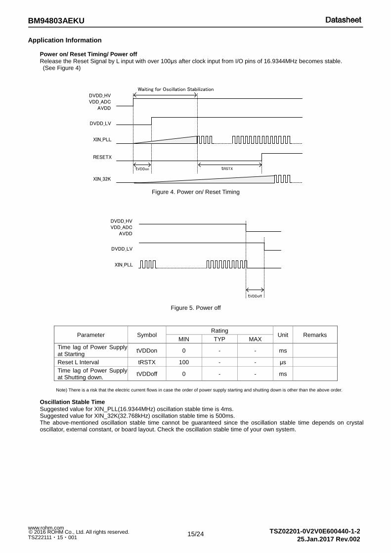
Application Information
Power on/ Reset Timing/ Power off
Release the Reset Signal by L input with over 100μs after clock input from I/O pins of 16.9344MHz becomes stable. (See Figure 4)
Figure 4. Power on/ Reset Timing
Figure 5. Power off
Parameter Symbol Rating
Unit Remarks MIN TYP MAX
Time lag of Power Supply at Starting
tVDDon 0 - - ms
Reset L Interval tRSTX 100 - - μs
Time lag of Power Supply at Shutting down.
tVDDoff 0 - - ms
Note) There is a risk that the electric current flows in case the order of power supply starting and shutting down is other than the above order.
Oscillation Stable Time
Suggested value for XIN_PLL(16.9344MHz) oscillation stable time is 4ms. Suggested value for XIN_32K(32.768kHz) oscillation stable time is 500ms. The above-mentioned oscillation stable time cannot be guaranteed since the oscillation stable time depends on crystal oscillator, external constant, or board layout. Check the oscillation stable time of your own system.
Waiting for Oscillation Stabilization
tRSTX
DVDD_HVVDD_ADC
AVDD
RESETX
XIN_PLL
DVDD_LV
tVDDon
XIN_32K
DVDD_HVVDD_ADC
AVDD
XIN_PLL
DVDD_LV
tVDDoff
16/24
BM94803AEKU
TSZ02201-0V2V0E600440-1-2
25.Jan.2017 Rev.002
© 2016 ROHM Co., Ltd. All rights reserved. www.rohm.com
TSZ22111・15・001
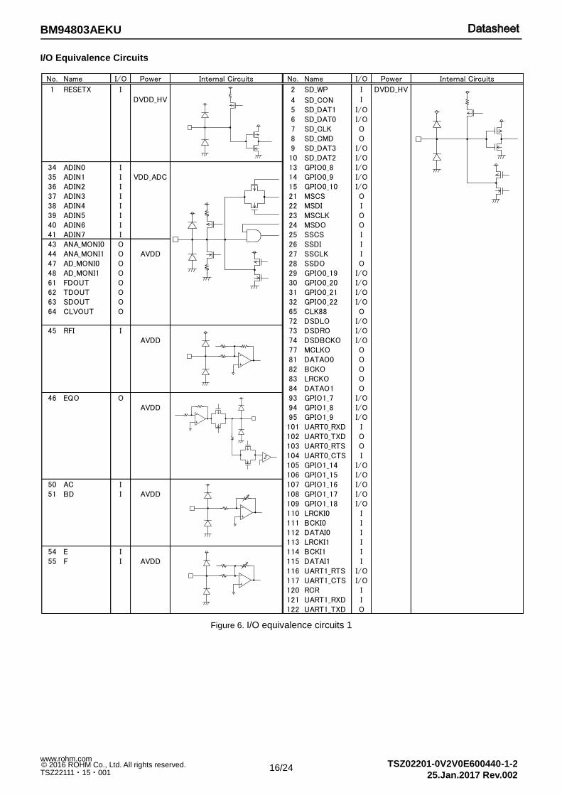
I/O Equivalence Circuits
Figure 6. I/O equivalence circuits 1
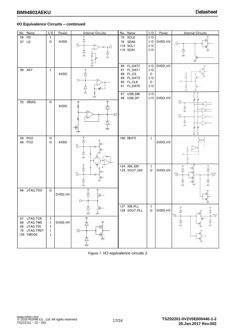
No. Name I/O Power Internal Circuits No. Name I/O Power Internal Circuits
1 RESETX I 2 SD_WP I DVDD_HV
DVDD_HV 4 SD_CON I
5 SD_DAT1 I/O6 SD_DAT0 I/O7 SD_CLK O8 SD_CMD O9 SD_DAT3 I/O10 SD_DAT2 I/O
34 ADIN0 I 13 GPIO0_8 I/O35 ADIN1 I VDD_ADC 14 GPIO0_9 I/O36 ADIN2 I 15 GPIO0_10 I/O37 ADIN3 I 21 MSCS O38 ADIN4 I 22 MSDI I39 ADIN5 I 23 MSCLK O40 ADIN6 I 24 MSDO O41 ADIN7 I 25 SSCS I43 ANA_MONI0 O 26 SSDI I44 ANA_MONI1 O AVDD 27 SSCLK I47 AD_MONI0 O 28 SSDO O48 AD_MONI1 O 29 GPIO0_19 I/O61 FDOUT O 30 GPIO0_20 I/O62 TDOUT O 31 GPIO0_21 I/O63 SDOUT O 32 GPIO0_22 I/O64 CLVOUT O 65 CLK88 O
72 DSDLO I/O45 RFI I 73 DSDRO I/O
AVDD 74 DSDBCKO I/O77 MCLKO O81 DATAO0 O82 BCKO O83 LRCKO O84 DATAO1 O
46 EQO O 93 GPIO1_7 I/OAVDD 94 GPIO1_8 I/O
95 GPIO1_9 I/O101 UART0_RXD I102 UART0_TXD O103 UART0_RTS O104 UART0_CTS I105 GPIO1_14 I/O106 GPIO1_15 I/O
50 AC I 107 GPIO1_16 I/O51 BD I AVDD 108 GPIO1_17 I/O
109 GPIO1_18 I/O110 LRCKI0 I111 BCKI0 I112 DATAI0 I113 LRCKI1 I
54 E I 114 BCKI1 I55 F I AVDD 115 DATAI1 I
116 UART1_RTS I/O117 UART1_CTS I/O120 RCR I121 UART1_RXD I122 UART1_TXD O
17/24
BM94803AEKU
TSZ02201-0V2V0E600440-1-2
25.Jan.2017 Rev.002
© 2016 ROHM Co., Ltd. All rights reserved. www.rohm.com
TSZ22111・15・001
I/O Equivalence Circuits – continued
Figure 7. I/O equivalence circuits 2
No. Name I/O Power Internal Circuits No. Name I/O Power Internal Circuits
56 PD I 75 SCL0 I/O
57 LD O AVDD 76 SDA0 I/O DVDD_HV
118 SCL1 I/O119 SDA1 I/O
86 FL_DAT2 I/O DVDD_HV58 ASY I 87 FL_DAT1 I/O
AVDD 88 FL_CS O89 FL_DAT3 I/O90 FL_CLK O91 FL_DAT0 I/O
97 USB_DM I/O98 USB_DP I/O DVDD_HV
52 VBIAS OAVDD
59 PCO O 100 REXTI I60 FCO O AVDD DVDD_HV
124 XIN_32K I125 XOUT_32K O DVDD_HV
66 JTAG_TDO ODVDD_HV
127 XIN_PLL I128 XOUT_PLL O DVDD_HV
67 JTAG_TCK I68 JTAG_TMS I DVDD_HV69 JTAG_TDI I70 JTAG_TRST I126 TMODE I
PCO
FCO
PD
LD
XIN_32K XOUT_32K
USB_DM
USB_DP
XIN_PLL XOUT_PLL
18/24
BM94803AEKU
TSZ02201-0V2V0E600440-1-2
25.Jan.2017 Rev.002
© 2016 ROHM Co., Ltd. All rights reserved. www.rohm.com
TSZ22111・15・001
Operational Notes1
1. About Compatibility in USB Memory Device and SD Memory Card According to the file structure and communication speed of USB memory, SD memory card, this LSI might not play back correctly.
2. About Compatibility in Bluetooth device
According to the type of Bluetooth device, , this LSI might not play back correctly.
3. About 2X Speed Recording Recording to a memory with slow access speed may require data connection operation. 2X speed recording to all the memories cannot be guaranteed.
4. Power OFF or Memory Disconnection Under Memory Writing
The sudden power off or memory disconnection during recording or file write operation to a memory may break the data in a memory.
5. Browsing Operation
With a memory with slow access speed, browsing operation during music playing may generate skipping.
6. CD-ROM Playing CD-ROM playing operation is premised on data being inputted so that an internal data buffer may not become empty. When an input does not meet the deadline and internal data buffers become empty, skipping occurs.
7. Playing Time of MP3 File
The playing time when MP3 file playing may shift when fast forward playing, rewind playing, and VBR playing.
8. Write-In Operation Exceeding Memory Size Writing to a file when memory size is exceeded is not supported.
9. Write-In Operation of the File Size Exceeding FAT Specification
Writing to a file when file size is exceeded is not supported.
10. About I2C Format I/F Although this LSI has adopted the I2C format, the level shifter circuit is not built in. For this reason, level shifter is needed for connection with the device besides the range of operating power supply voltage of this LSI.
11. CD Media Playing According to the condition of CD media, flawed, dirty, curved, eccentric and etc., this LSI might not play back normally.
12. Application Block Diagram Each software function of Audio Encoder, Audio Decoder, BT stack A2DP, SBC Decoder and File System(FTA12/16/32, ISO9660) described in Figure 1. Application Block are realized by downloading applicable program from external Serial Flash ROM.
19/24
BM94803AEKU
TSZ02201-0V2V0E600440-1-2
25.Jan.2017 Rev.002
© 2016 ROHM Co., Ltd. All rights reserved. www.rohm.com
TSZ22111・15・001
Operational Notes2
1. Reverse Connection of Power Supply Connecting the power supply in reverse polarity can damage the IC. Take precautions against reverse polarity when connecting the power supply, such as mounting an external diode between the power supply and the IC’s power supply pins.
2. Power Supply Lines
Design the PCB layout pattern to provide low impedance supply lines. Separate the ground and supply lines of the digital and analog blocks to prevent noise in the ground and supply lines of the digital block from affecting the analog block. Furthermore, connect a capacitor to ground at all power supply pins. Consider the effect of temperature and aging on the capacitance value when using electrolytic capacitors.
3. Ground Voltage
Ensure that no pins are at a voltage below that of the ground pin at any time, even during transient condition.
4. Ground Wiring Pattern When using both small-signal and large-current ground traces, the two ground traces should be routed separately but connected to a single ground at the reference point of the application board to avoid fluctuations in the small-signal ground caused by large currents. Also ensure that the ground traces of external components do not cause variations on the ground voltage. The ground lines must be as short and thick as possible to reduce line impedance.
5. Thermal Consideration
Should by any chance the maximum junction temperature rating be exceeded the rise in temperature of the chip may result in deterioration of the properties of the chip. In case of exceeding this absolute maximum rating, increase the board size and copper area to prevent exceeding the maximum junction temperature rating.
6. Recommended Operating Conditions
These conditions represent a range within which the expected characteristics of the IC can be approximately obtained. The electrical characteristics are guaranteed under the conditions of each parameter.
7. Inrush Current
When power is first supplied to the IC, it is possible that the internal logic may be unstable and inrush current may flow instantaneously due to the internal powering sequence and delays, especially if the IC has more than one power supply. Therefore, give special consideration to power coupling capacitance, power wiring, width of ground wiring, and routing of connections.
8. Operation Under Strong Electromagnetic Field Operating the IC in the presence of a strong electromagnetic field may cause the IC to malfunction.
20/24
BM94803AEKU
TSZ02201-0V2V0E600440-1-2
25.Jan.2017 Rev.002
© 2016 ROHM Co., Ltd. All rights reserved. www.rohm.com
TSZ22111・15・001
Operational Notes2 – continued
9. Testing on Application Boards When testing the IC on an application board, connecting a capacitor directly to a low-impedance output pin may subject the IC to stress. Always discharge capacitors completely after each process or step. The IC’s power supply should always be turned off completely before connecting or removing it from the test setup during the inspection process. To prevent damage from static discharge, ground the IC during assembly and use similar precautions during transport and storage.
10. Inter-pin Short and Mounting Errors
Ensure that the direction and position are correct when mounting the IC on the PCB. Incorrect mounting may result in damaging the IC. Avoid nearby pins being shorted to each other especially to ground, power supply and output pin. Inter-pin shorts could be due to many reasons such as metal particles, water droplets (in very humid environment) and unintentional solder bridge deposited in between pins during assembly to name a few.
11. Unused Input Pins
Input pins of an IC are often connected to the gate of a MOS transistor. The gate has extremely high impedance and extremely low capacitance. If left unconnected, the electric field from the outside can easily charge it. The small charge acquired in this way is enough to produce a significant effect on the conduction through the transistor and cause unexpected operation of the IC. So unless otherwise specified, unused input pins should be connected to the power supply or ground line.
12. Regarding the Input Pin of the IC
In the construction of this IC, P-N junctions are inevitably formed creating parasitic diodes or transistors. The operation of these parasitic elements can result in mutual interference among circuits, operational faults, or physical damage. Therefore, conditions which cause these parasitic elements to operate, such as applying a voltage to an input pin lower than the ground voltage should be avoided. Furthermore, do not apply a voltage to the input pins when no power supply voltage is applied to the IC. Even if the power supply voltage is applied, make sure that the input pins have voltages within the values specified in the electrical characteristics of this IC.
13. Ceramic Capacitor
When using a ceramic capacitor, determine the dielectric constant considering the change of capacitance with temperature and the decrease in nominal capacitance due to DC bias and others.
21/24
BM94803AEKU
TSZ02201-0V2V0E600440-1-2
25.Jan.2017 Rev.002
© 2016 ROHM Co., Ltd. All rights reserved. www.rohm.com
TSZ22111・15・001
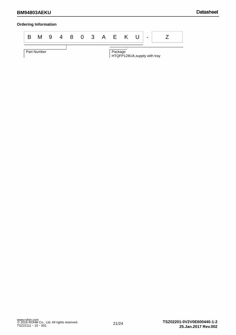
Ordering Information
B M 9 4 8 0 3 A E K U - Z
Part Number
Package HTQFP128UA,supply with tray
22/24
BM94803AEKU
TSZ02201-0V2V0E600440-1-2
25.Jan.2017 Rev.002
© 2016 ROHM Co., Ltd. All rights reserved. www.rohm.com
TSZ22111・15・001
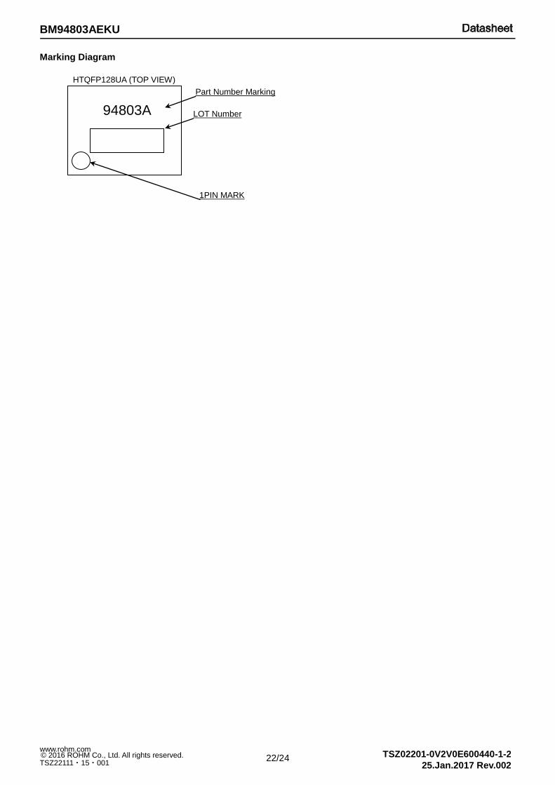
Marking Diagram
HTQFP128UA (TOP VIEW)
94803A
Part Number Marking
LOT Number
1PIN MARK
23/24
BM94803AEKU
TSZ02201-0V2V0E600440-1-2
25.Jan.2017 Rev.002
© 2016 ROHM Co., Ltd. All rights reserved. www.rohm.com
TSZ22111・15・001
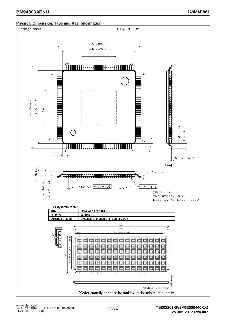
Physical Dimension, Tape and Reel Information
Package Name HTQFP128UA
24/24
BM94803AEKU
TSZ02201-0V2V0E600440-1-2
25.Jan.2017 Rev.002
© 2016 ROHM Co., Ltd. All rights reserved. www.rohm.com
TSZ22111・15・001
Revision History
Date Revision Changes
30.Aug.2016 001 New Release
25.Jan.2017 002
P10: Modified Block name of 118/119pin to I2C. P11: Modified pin name of Serial Flash ROM from SCLK to SIO3. P14: Modified pin name FLAG1 to GPIO1_7, FLAG2 to GPIO1_8, VC to VBIAS, and removed ASY_TEST, APCREF in Electrical Characteristics. P18: Added Note about Application Block diagram.
Notice-PGA-E Rev.003
© 2015 ROHM Co., Ltd. All rights reserved.
Notice
Precaution on using ROHM Products 1. Our Products are designed and manufactured for application in ordinary electronic equipments (such as AV equipment,
OA equipment, telecommunication equipment, home electronic appliances, amusement equipment, etc.). If you intend to use our Products in devices requiring extremely high reliability (such as medical equipment
(Note 1), transport
equipment, traffic equipment, aircraft/spacecraft, nuclear power controllers, fuel controllers, car equipment including car accessories, safety devices, etc.) and whose malfunction or failure may cause loss of human life, bodily injury or serious damage to property (“Specific Applications”), please consult with the ROHM sales representative in advance. Unless otherwise agreed in writing by ROHM in advance, ROHM shall not be in any way responsible or liable for any damages, expenses or losses incurred by you or third parties arising from the use of any ROHM’s Products for Specific Applications.
(Note1) Medical Equipment Classification of the Specific Applications
JAPAN USA EU CHINA
CLASSⅢ CLASSⅢ
CLASSⅡb CLASSⅢ
CLASSⅣ CLASSⅢ
2. ROHM designs and manufactures its Products subject to strict quality control system. However, semiconductor
products can fail or malfunction at a certain rate. Please be sure to implement, at your own responsibilities, adequate safety measures including but not limited to fail-safe design against the physical injury, damage to any property, which a failure or malfunction of our Products may cause. The following are examples of safety measures:
[a] Installation of protection circuits or other protective devices to improve system safety [b] Installation of redundant circuits to reduce the impact of single or multiple circuit failure
3. Our Products are designed and manufactured for use under standard conditions and not under any special or extraordinary environments or conditions, as exemplified below. Accordingly, ROHM shall not be in any way responsible or liable for any damages, expenses or losses arising from the use of any ROHM’s Products under any special or extraordinary environments or conditions. If you intend to use our Products under any special or extraordinary environments or conditions (as exemplified below), your independent verification and confirmation of product performance, reliability, etc, prior to use, must be necessary:
[a] Use of our Products in any types of liquid, including water, oils, chemicals, and organic solvents [b] Use of our Products outdoors or in places where the Products are exposed to direct sunlight or dust [c] Use of our Products in places where the Products are exposed to sea wind or corrosive gases, including Cl2,
H2S, NH3, SO2, and NO2
[d] Use of our Products in places where the Products are exposed to static electricity or electromagnetic waves [e] Use of our Products in proximity to heat-producing components, plastic cords, or other flammable items [f] Sealing or coating our Products with resin or other coating materials [g] Use of our Products without cleaning residue of flux (even if you use no-clean type fluxes, cleaning residue of
flux is recommended); or Washing our Products by using water or water-soluble cleaning agents for cleaning residue after soldering
[h] Use of the Products in places subject to dew condensation
4. The Products are not subject to radiation-proof design. 5. Please verify and confirm characteristics of the final or mounted products in using the Products. 6. In particular, if a transient load (a large amount of load applied in a short period of time, such as pulse. is applied,
confirmation of performance characteristics after on-board mounting is strongly recommended. Avoid applying power exceeding normal rated power; exceeding the power rating under steady-state loading condition may negatively affect product performance and reliability.
7. De-rate Power Dissipation depending on ambient temperature. When used in sealed area, confirm that it is the use in
the range that does not exceed the maximum junction temperature. 8. Confirm that operation temperature is within the specified range described in the product specification. 9. ROHM shall not be in any way responsible or liable for failure induced under deviant condition from what is defined in
this document.
Precaution for Mounting / Circuit board design 1. When a highly active halogenous (chlorine, bromine, etc.) flux is used, the residue of flux may negatively affect product
performance and reliability.
2. In principle, the reflow soldering method must be used on a surface-mount products, the flow soldering method must be used on a through hole mount products. If the flow soldering method is preferred on a surface-mount products, please consult with the ROHM representative in advance.
For details, please refer to ROHM Mounting specification
Notice-PGA-E Rev.003
© 2015 ROHM Co., Ltd. All rights reserved.
Precautions Regarding Application Examples and External Circuits 1. If change is made to the constant of an external circuit, please allow a sufficient margin considering variations of the
characteristics of the Products and external components, including transient characteristics, as well as static characteristics.
2. You agree that application notes, reference designs, and associated data and information contained in this document
are presented only as guidance for Products use. Therefore, in case you use such information, you are solely responsible for it and you must exercise your own independent verification and judgment in the use of such information contained in this document. ROHM shall not be in any way responsible or liable for any damages, expenses or losses incurred by you or third parties arising from the use of such information.
Precaution for Electrostatic This Product is electrostatic sensitive product, which may be damaged due to electrostatic discharge. Please take proper caution in your manufacturing process and storage so that voltage exceeding the Products maximum rating will not be applied to Products. Please take special care under dry condition (e.g. Grounding of human body / equipment / solder iron, isolation from charged objects, setting of Ionizer, friction prevention and temperature / humidity control).
Precaution for Storage / Transportation 1. Product performance and soldered connections may deteriorate if the Products are stored in the places where:
[a] the Products are exposed to sea winds or corrosive gases, including Cl2, H2S, NH3, SO2, and NO2 [b] the temperature or humidity exceeds those recommended by ROHM [c] the Products are exposed to direct sunshine or condensation [d] the Products are exposed to high Electrostatic
2. Even under ROHM recommended storage condition, solderability of products out of recommended storage time period may be degraded. It is strongly recommended to confirm solderability before using Products of which storage time is exceeding the recommended storage time period.
3. Store / transport cartons in the correct direction, which is indicated on a carton with a symbol. Otherwise bent leads
may occur due to excessive stress applied when dropping of a carton. 4. Use Products within the specified time after opening a humidity barrier bag. Baking is required before using Products of
which storage time is exceeding the recommended storage time period.
Precaution for Product Label A two-dimensional barcode printed on ROHM Products label is for ROHM’s internal use only.
Precaution for Disposition When disposing Products please dispose them properly using an authorized industry waste company.
Precaution for Foreign Exchange and Foreign Trade act Since concerned goods might be fallen under listed items of export control prescribed by Foreign exchange and Foreign trade act, please consult with ROHM in case of export.
Precaution Regarding Intellectual Property Rights 1. All information and data including but not limited to application example contained in this document is for reference
only. ROHM does not warrant that foregoing information or data will not infringe any intellectual property rights or any other rights of any third party regarding such information or data.
2. ROHM shall not have any obligations where the claims, actions or demands arising from the combination of the Products with other articles such as components, circuits, systems or external equipment (including software).
3. No license, expressly or implied, is granted hereby under any intellectual property rights or other rights of ROHM or any third parties with respect to the Products or the information contained in this document. Provided, however, that ROHM will not assert its intellectual property rights or other rights against you or your customers to the extent necessary to manufacture or sell products containing the Products, subject to the terms and conditions herein.
Other Precaution 1. This document may not be reprinted or reproduced, in whole or in part, without prior written consent of ROHM.
2. The Products may not be disassembled, converted, modified, reproduced or otherwise changed without prior written consent of ROHM.
3. In no event shall you use in any way whatsoever the Products and the related technical information contained in the Products or this document for any military purposes, including but not limited to, the development of mass-destruction weapons.
4. The proper names of companies or products described in this document are trademarks or registered trademarks of ROHM, its affiliated companies or third parties.
DatasheetDatasheet
Notice – WE Rev.001© 2015 ROHM Co., Ltd. All rights reserved.
General Precaution 1. Before you use our Pro ducts, you are requested to care fully read this document and fully understand its contents.
ROHM shall n ot be in an y way responsible or liabl e for fa ilure, malfunction or acci dent arising from the use of a ny ROHM’s Products against warning, caution or note contained in this document.
2. All information contained in this docume nt is current as of the issuing date and subj ect to change without any prior
notice. Before purchasing or using ROHM’s Products, please confirm the la test information with a ROHM sale s representative.
3. The information contained in this doc ument is provi ded on an “as is” basis and ROHM does not warrant that all
information contained in this document is accurate an d/or error-free. ROHM shall not be in an y way responsible or liable for any damages, expenses or losses incurred by you or third parties resulting from inaccuracy or errors of or concerning such information.