Embed Size (px)
Citation preview
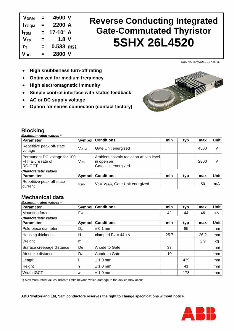
ABB Switzerland Ltd, Semiconductors reserves the right to change specifications without notice.
VDRM = 4500 V Reverse Conducting Integrated
Gate-Commutated Thyristor
5SHX 26L4520
ITGQM = 2200 A
ITSM = 17·103 A
VT0 = 1.8 V
rT = 0.533 m
VDC = 2800 V
Doc. No. 5SYA1251-01 Apr. 16
High snubberless turn-off rating
Optimized for medium frequency
High electromagnetic immunity
Simple control interface with status feedback
AC or DC supply voltage
Option for series connection (contact factory)
Blocking Maximum rated values 1)
Parameter Symbol Conditions min typ max Unit
Repetitive peak off-state voltage
VDRM Gate Unit energized 4500 V
Permanent DC voltage for 100 FIT failure rate of RC-GCT
VDC Ambient cosmic radiation at sea level in open air. Gate Unit energized
2800 V
Characteristic values
Parameter Symbol Conditions min typ max Unit
Repetitive peak off-state current
IDRM VD = VDRM, Gate Unit energized 50 mA
Mechanical data Maximum rated values 1)
Parameter Symbol Conditions min typ max Unit
Mounting force FM 42 44 46 kN
Characteristic values
Parameter Symbol Conditions min typ max Unit
Pole-piece diameter Dp ± 0.1 mm 85 mm
Housing thickness H clamped Fm = 44 kN 25.7 26.2 mm
Weight m 2.9 kg
Surface creepage distance DS Anode to Gate 33 mm
Air strike distance Da Anode to Gate 10 mm
Length l ± 1.0 mm 439 mm
Height h ± 1.0 mm 41 mm
Width IGCT w ± 1.0 mm 173 mm
1) Maximum rated values indicate limits beyond which damage to the device may occur
5SHX 26L4520
ABB Switzerland Ltd, Semiconductors reserves the right to change specifications without notice. Doc. No. 5SYA1251-01 Apr. 16 page 2 of 14
GCT Data
On-state Maximum rated values 1)
Parameter Symbol Conditions min typ max Unit
Average on-state current IT(AV)M Half sine wave, Tc = 85 °C
1010 A
RMS on-state current IT(RMS) 1590 A
Peak non-repetitive surge current
ITSM tp = 3 ms, Tv j= 125 °C sine half wave VD = VR = 0 V, after surge
25·103 A
Limiting load integral I2t 938·103 A2s
Peak non-repetitive surge current
ITSM tp = 10 ms, Tvj = 125 °C sine half wave VD = VR = 0 V, after surge
17·103 A
Limiting load integral I2t 1.45·106 A2s
Peak non-repetitive surge current
ITSM tp = 30 ms, Tvj = 125 °C sine half wave VD = VR = 0 V, after surge
13·103 A
Limiting load integral I2t 2.55·106 A2s
Critical rate of rise of onstate current
diT/dt(cr)
For higher diT/dt and current lower than 100 A an external retrigger puls is required.
100 A/µs
Characteristic values
Parameter Symbol Conditions min typ max Unit
On-state voltage VT IT = 2200 A, Tvj = 125 °C 2.3 2.6 2.95 V
Threshold voltage V(T0) IT = 400 A - 3000 A, Tvj = 125 °C
1.8 V
Slope resistance rT 0.533 m
5SHX 26L4520
ABB Switzerland Ltd, Semiconductors reserves the right to change specifications without notice. Doc. No. 5SYA1251-01 Apr. 16 page 3 of 14
Turn-on switching Maximum rated values 1)
Parameter Symbol Conditions min typ max Unit
Critical rate of rise of on-state current
di/dtcrit f = 0 - 500 Hz, Tvj = 125 °C IT = 2200 A, VD = 2800 V ITM ≤ 2640, DCL = 5SDF 10H4503
650 A/µs
Characteristic values
Parameter Symbol Conditions min typ max Unit
Turn-on delay time td(on) Tvj = 125 °C VD = 2800 V, IT = 2200 A di/dt = VD / Li, Li = 5 µH CCL = 10 µf, LCL = 300 nH DCL = 5SDF 10H4503
3.5 µs
Turn-on delay time status feedback
td(on) SF 7 µs
Rise time tr 1 µs
Turn-on energy per pulse Eon 0.85 J
Turn-off switching Maximum rated values 1)
Parameter Symbol Conditions min typ max Unit
Controllable turn-off current
ITGQM1 VDM VDRM Tvj = 125 °C
RS = 0.65 CCL = 10 µF
LCL 300 nH DCL = 5SDF 10H4503
VD = 2800 V
2200 A
ITGQM2
VD = 3200 V
1100 A
Characteristic values
Parameter Symbol Conditions min typ max Unit
Turn-off delay time td(off) VD = 2800, Tvj = 125 °C VDM ≤ VDRM, Rs = 0.65 Ω ITGQ = 2200 A, Li = 5 µH CCL = 10 µF, LCL = 300 nH DCL = 5SDF 10H4503
7 µs
Turn-off delay time status feedback
td(off) SF 7 µs
Turn-off energy per pulse Eoff 7.8 12 J
5SHX 26L4520
ABB Switzerland Ltd, Semiconductors reserves the right to change specifications without notice. Doc. No. 5SYA1251-01 Apr. 16 page 4 of 14
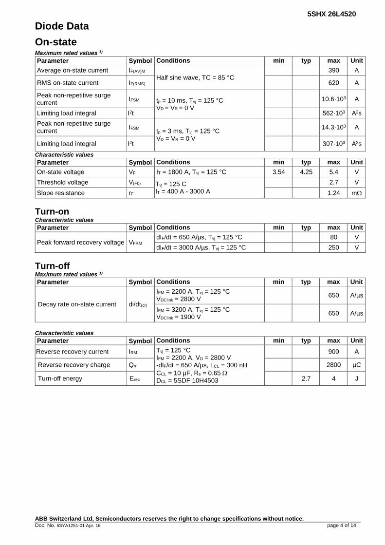
Diode Data
On-state Maximum rated values 1)
Parameter Symbol Conditions min typ max Unit
Average on-state current IF(AV)M Half sine wave, TC = 85 °C
390 A
RMS on-state current IF(RMS) 620 A
Peak non-repetitive surge current
IFSM tp = 10 ms, Tvj = 125 °C VD = VR = 0 V
10.6·103 A
Limiting load integral I2t 562·103 A2s
Peak non-repetitive surge current
IFSM tp = 3 ms, Tvj = 125 °C VD = VR = 0 V
14.3·103 A
Limiting load integral I2t 307·103 A2s
Characteristic values
Parameter Symbol Conditions min typ max Unit
On-state voltage VF IT = 1800 A, Tvj = 125 °C 3.54 4.25 5.4 V
Threshold voltage V(F0) Tvj = 125 C IT = 400 A - 3000 A
2.7 V
Slope resistance rF 1.24 m
Turn-on Characteristic values
Parameter Symbol Conditions min typ max Unit
Peak forward recovery voltage VFRM dIF/dt = 650 A/µs, Tvj = 125 °C 80 V
dIF/dt = 3000 A/µs, Tvj = 125 °C 250 V
Turn-off Maximum rated values 1)
Parameter Symbol Conditions min typ max Unit
Decay rate on-state current di/dt(cr)
IFM = 2200 A, Tvj = 125 °C VDClink = 2800 V 650 A/µs
IFM = 3200 A, Tvj = 125 °C VDClink = 1900 V 650 A/µs
Characteristic values
Parameter Symbol Conditions min typ max Unit
Reverse recovery current IRM Tvj = 125 °C IFM = 2200 A, VD = 2800 V -dIF/dt = 650 A/µs, LCL = 300 nH
CCL = 10 µF, Rs = 0.65 DCL = 5SDF 10H4503
900 A
Reverse recovery charge Qrr 2800 µC
Turn-off energy Erec 2.7 4 J
5SHX 26L4520
ABB Switzerland Ltd, Semiconductors reserves the right to change specifications without notice. Doc. No. 5SYA1251-01 Apr. 16 page 5 of 14
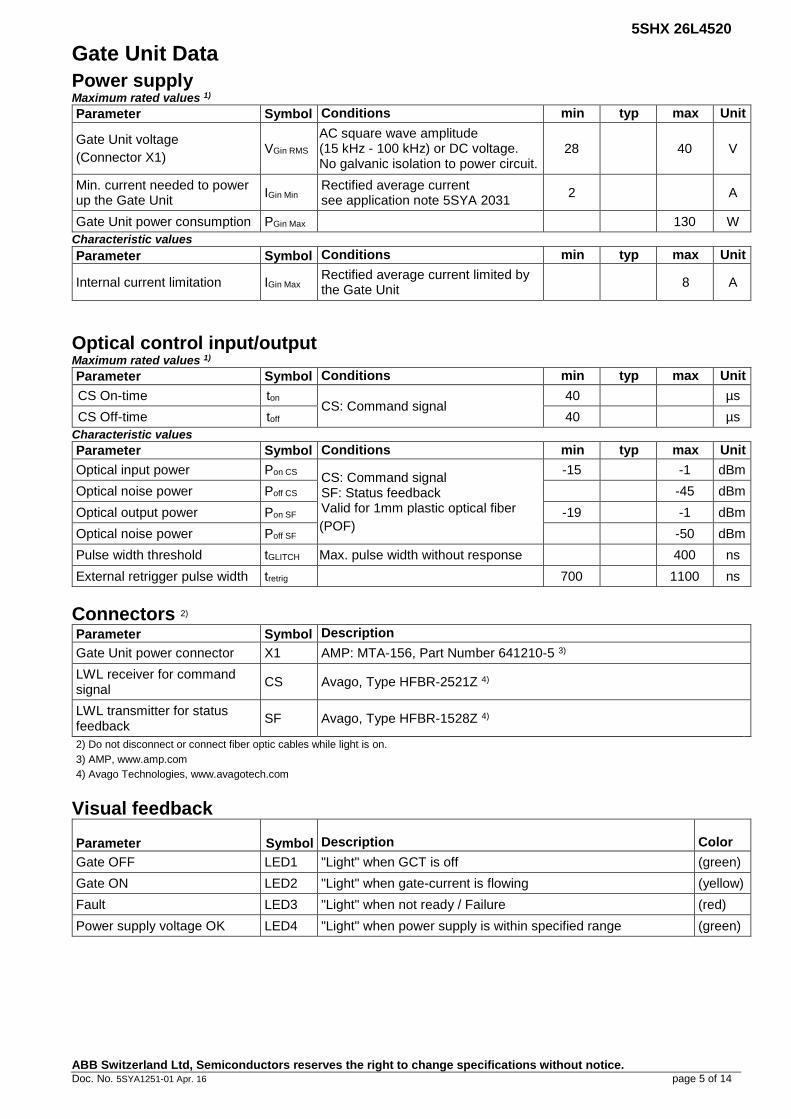
Gate Unit Data
Power supply Maximum rated values 1)
Parameter Symbol Conditions min typ max Unit
Gate Unit voltage
(Connector X1) VGin RMS
AC square wave amplitude (15 kHz - 100 kHz) or DC voltage. No galvanic isolation to power circuit.
28 40 V
Min. current needed to power up the Gate Unit
IGin Min Rectified average current see application note 5SYA 2031
2 A
Gate Unit power consumption PGin Max 130 W Characteristic values
Parameter Symbol Conditions min typ max Unit
Internal current limitation IGin Max Rectified average current limited by the Gate Unit
8 A
Optical control input/output Maximum rated values 1)
Parameter Symbol Conditions min typ max Unit
CS On-time ton CS: Command signal
40 µs
CS Off-time toff 40 µs
Characteristic values
Parameter Symbol Conditions min typ max Unit
Optical input power Pon CS CS: Command signal SF: Status feedback Valid for 1mm plastic optical fiber
(POF)
-15 -1 dBm
Optical noise power Poff CS -45 dBm
Optical output power Pon SF -19 -1 dBm
Optical noise power Poff SF -50 dBm
Pulse width threshold tGLITCH Max. pulse width without response 400 ns
External retrigger pulse width tretrig 700 1100 ns
Connectors 2) Parameter Symbol Description
Gate Unit power connector X1 AMP: MTA-156, Part Number 641210-5 3)
LWL receiver for command signal
CS Avago, Type HFBR-2521Z 4)
LWL transmitter for status feedback
SF Avago, Type HFBR-1528Z 4)
2) Do not disconnect or connect fiber optic cables while light is on.
3) AMP, www.amp.com 4) Avago Technologies, www.avagotech.com
Visual feedback
Parameter Symbol Description Color
Gate OFF LED1 "Light" when GCT is off (green)
Gate ON LED2 "Light" when gate-current is flowing (yellow)
Fault LED3 "Light" when not ready / Failure (red)
Power supply voltage OK LED4 "Light" when power supply is within specified range (green)
5SHX 26L4520
ABB Switzerland Ltd, Semiconductors reserves the right to change specifications without notice. Doc. No. 5SYA1251-01 Apr. 16 page 6 of 14
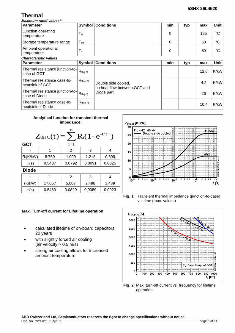
Thermal Maximum rated values 1)
Parameter Symbol Conditions min typ max Unit
Junction operating temperature
Tvj 0 125 °C
Storage temperature range Tstg 0 60 °C
Ambient operational temperature
Ta 0 50 °C
Characteristic values
Analytical function for transient thermal impedance:
GCT
)e-(1R = (t)Zn
1i
t/-i thJC
i
i 1 2 3 4
Ri(K/kW) 8.769 1.909 1.218 0.699
i(s) 0.5407 0.0792 0.0091 0.0025
Diode
i 1 2 3 4
(K/kW) 17.057 5.007 2.498 1.439
i(s) 0.5460 0.0829 0.0089 0.0023
Fig. 1 Transient thermal impedance (junction-to-case) vs. time (max. values)
Max. Turn-off current for Lifetime operation
calculated lifetime of on-board capacitors 20 years
with slightly forced air cooling (air velocity > 0.5 m/s)
strong air cooling allows for increased ambient temperature
Fig. 2 Max. turn-off current vs. frequency for lifetime operation
Parameter Symbol Conditions min typ max Unit
Thermal resistance junction-to-case of GCT
Rth(j-c)
Double side cooled, no heat flow between GCT and Diode part
12.6 K/kW
Thermal resistance case-to-heatsink of GCT
Rth(c-h) 4.2 K/kW
Thermal resistance junction-to-case of Diode
Rth(j-c) 26 K/kW
Thermal resistance case-to-heatsink of Diode
Rth(c-h) 10.4 K/kW
5SHX 26L4520
ABB Switzerland Ltd, Semiconductors reserves the right to change specifications without notice. Doc. No. 5SYA1251-01 Apr. 16 page 7 of 14
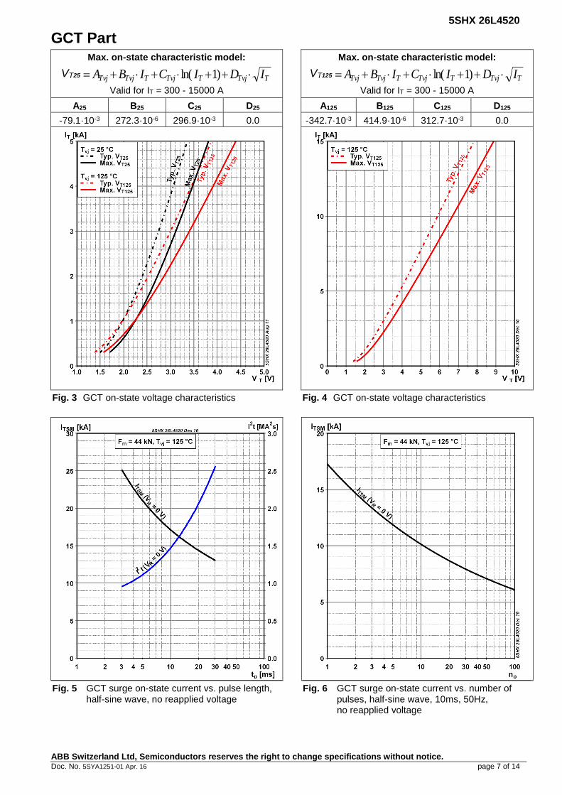
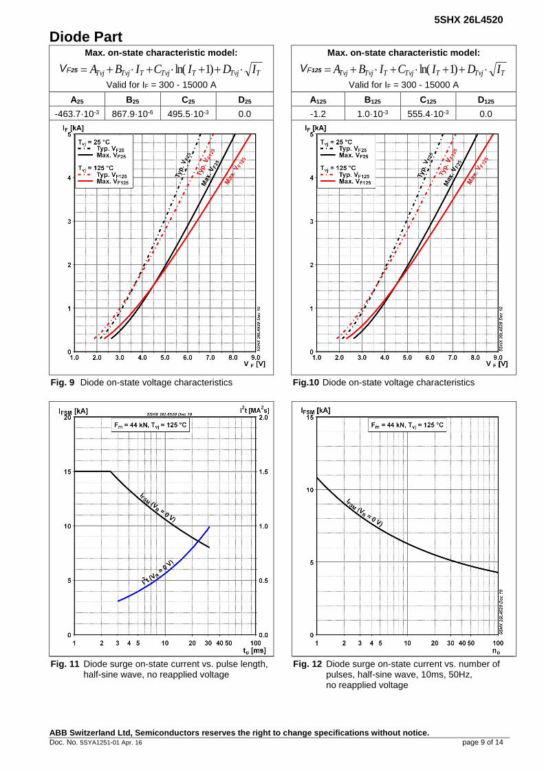
GCT Part Max. on-state characteristic model:
VT25 TTvjTTvjTTvjTvj IDICIBA )1ln( Valid for IT = 300 - 15000 A
Max. on-state characteristic model:
VT125 TTvjTTvjTTvjTvj IDICIBA )1ln(
Valid for IT = 300 - 15000 A
A25 B25 C25 D25 A125 B125 C125 D125
-79.1·10-3 272.3·10-6 296.9·10-3 0.0 -342.7·10-3 414.9·10-6 312.7·10-3 0.0
Fig. 3 GCT on-state voltage characteristics Fig. 4 GCT on-state voltage characteristics
Fig. 5 GCT surge on-state current vs. pulse length, half-sine wave, no reapplied voltage
Fig. 6 GCT surge on-state current vs. number of pulses, half-sine wave, 10ms, 50Hz, no reapplied voltage
5SHX 26L4520
ABB Switzerland Ltd, Semiconductors reserves the right to change specifications without notice. Doc. No. 5SYA1251-01 Apr. 16 page 8 of 14
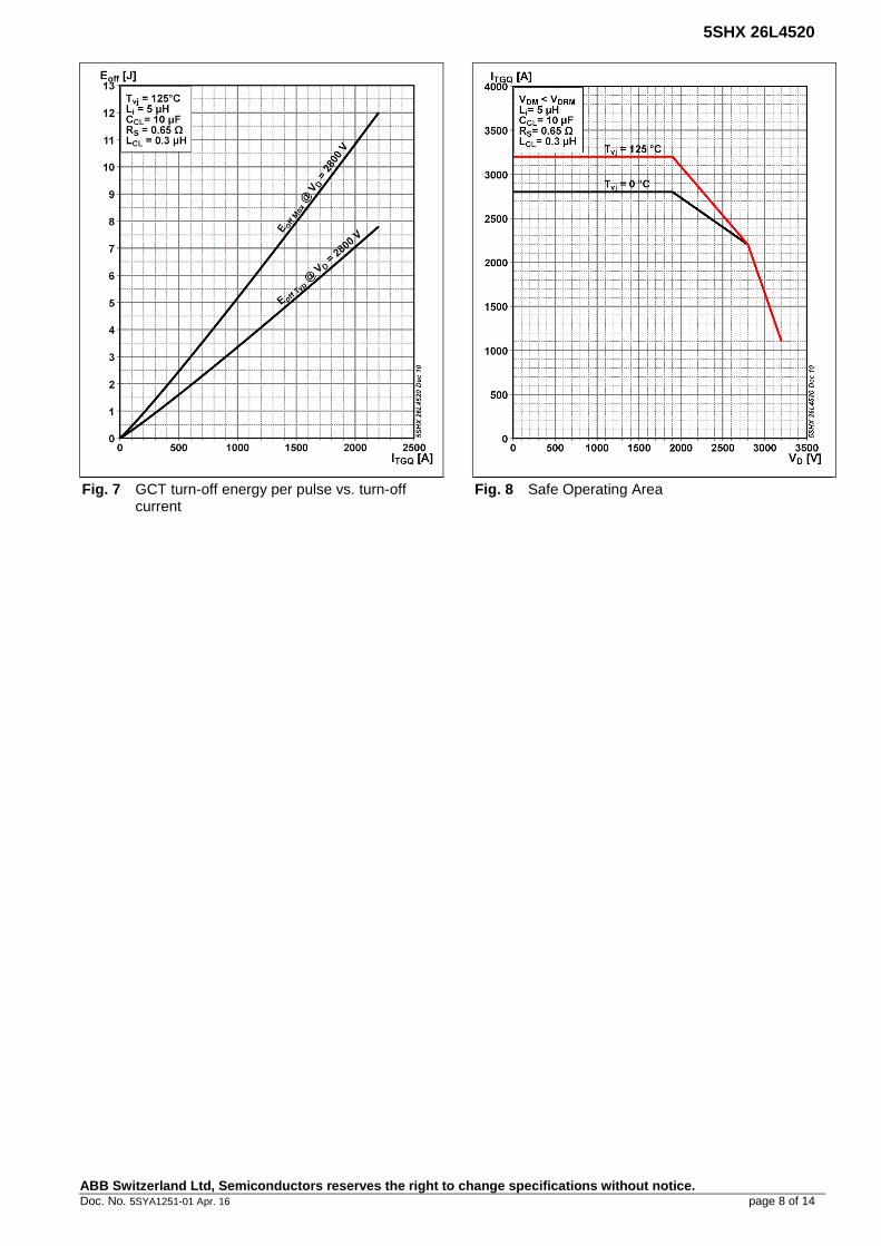
Fig. 7 GCT turn-off energy per pulse vs. turn-off current
Fig. 8 Safe Operating Area
5SHX 26L4520
ABB Switzerland Ltd, Semiconductors reserves the right to change specifications without notice. Doc. No. 5SYA1251-01 Apr. 16 page 9 of 14
Diode Part Max. on-state characteristic model:
VF25 TTvjTTvjTTvjTvj IDICIBA )1ln( Valid for IF = 300 - 15000 A
Max. on-state characteristic model:
VF125 TTvjTTvjTTvjTvj IDICIBA )1ln(
Valid for IF = 300 - 15000 A
A25 B25 C25 D25 A125 B125 C125 D125
-463.7·10-3 867.9·10-6 495.5·10-3 0.0 -1.2 1.0·10-3 555.4·10-3 0.0
Fig. 9 Diode on-state voltage characteristics Fig.10 Diode on-state voltage characteristics
Fig. 11 Diode surge on-state current vs. pulse length, half-sine wave, no reapplied voltage
Fig. 12 Diode surge on-state current vs. number of pulses, half-sine wave, 10ms, 50Hz, no reapplied voltage
5SHX 26L4520
ABB Switzerland Ltd, Semiconductors reserves the right to change specifications without notice. Doc. No. 5SYA1251-01 Apr. 16 page 10 of 14
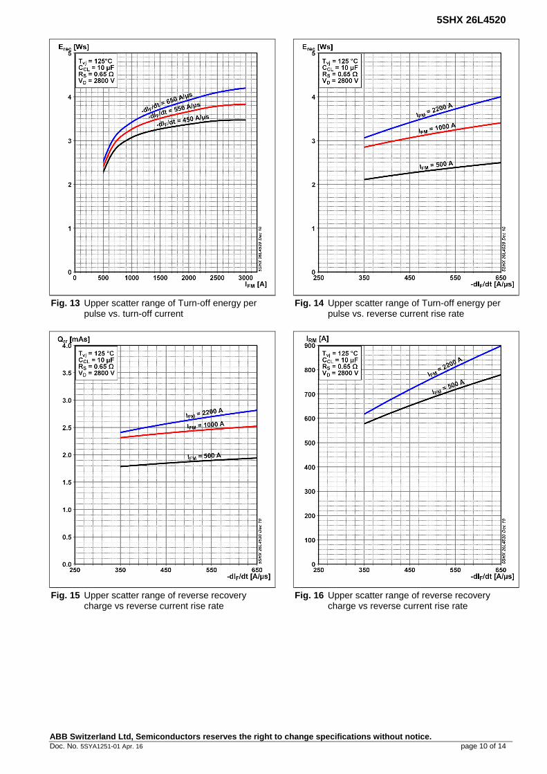
Fig. 13 Upper scatter range of Turn-off energy per pulse vs. turn-off current
Fig. 14 Upper scatter range of Turn-off energy per pulse vs. reverse current rise rate
Fig. 15 Upper scatter range of reverse recovery charge vs reverse current rise rate
Fig. 16 Upper scatter range of reverse recovery charge vs reverse current rise rate
5SHX 26L4520
ABB Switzerland Ltd, Semiconductors reserves the right to change specifications without notice. Doc. No. 5SYA1251-01 Apr. 16 page 11 of 14
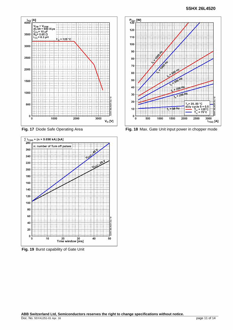
Fig. 17 Diode Safe Operating Area Fig. 18 Max. Gate Unit input power in chopper mode
Fig. 19 Burst capability of Gate Unit
5SHX 26L4520
ABB Switzerland Ltd, Semiconductors reserves the right to change specifications without notice. Doc. No. 5SYA1251-01 Apr. 16 page 12 of 14
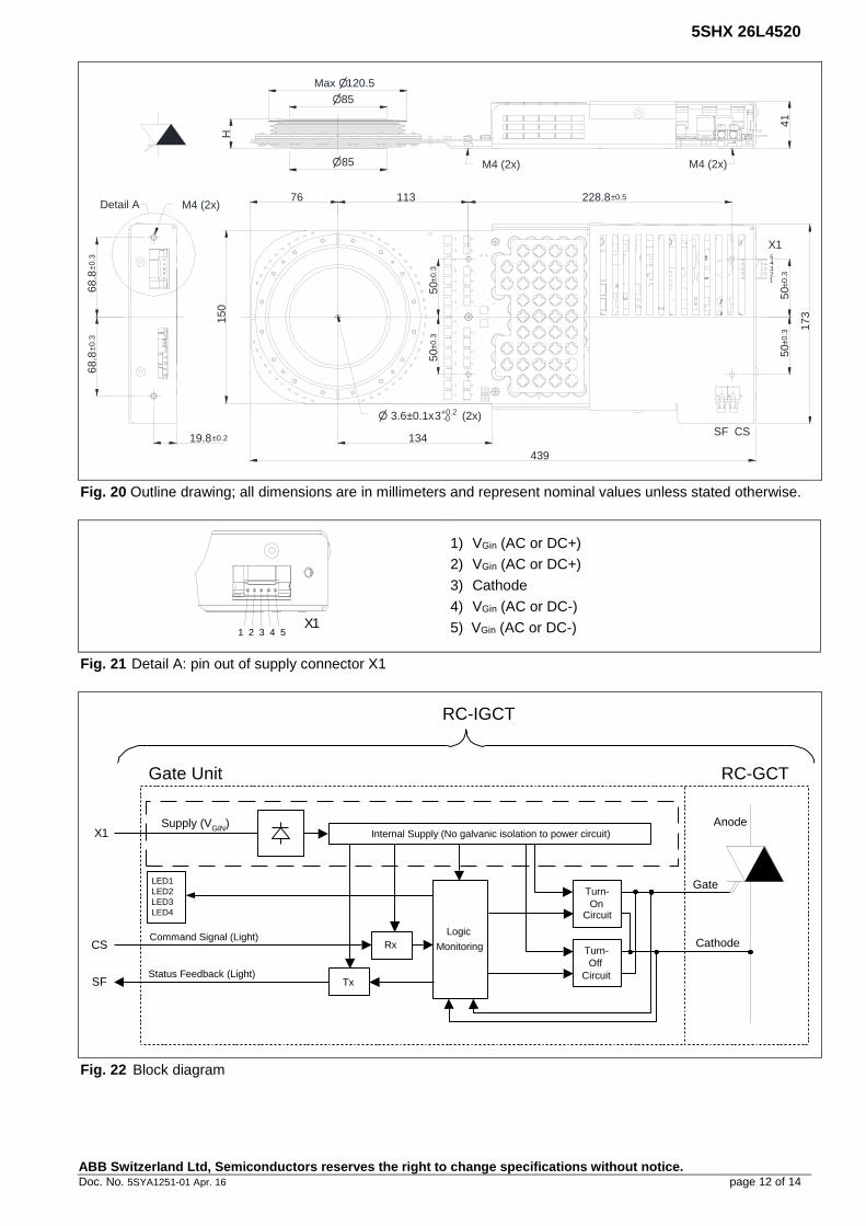
Fig. 20 Outline drawing; all dimensions are in millimeters and represent nominal values unless stated otherwise.
1) VGin (AC or DC+)
2) VGin (AC or DC+)
3) Cathode
4) VGin (AC or DC-)
5) VGin (AC or DC-)
Fig. 21 Detail A: pin out of supply connector X1
Fig. 22 Block diagram
3.6±0.1x (2x)
150
173
439
50
±0
.35
0±0
.3
228.8±0.5
134
113
50
±0
.35
0±0
.3
76 M4 (2x)
68.8
±0
.36
8.8
±0
.3
19.8±0.2
M4 (2x) M4 (2x)
H
Max 120.5
85
85
41
3+0.2-0
SF CS
54321
X1
Detail A
1 2 3 4 5X1
Logic
Monitoring Turn-
Off
Circuit
Turn-
OnCircuit
Gate
Cathode
Internal Supply (No galvanic isolation to power circuit)Supply (V
GIN)
X1
CS
LED1
LED2
LED3
LED4
RxCommand Signal (Light)
TxStatus Feedback (Light)
Anode
SF
RC-IGCT
Gate Unit RC-GCT
5SHX 26L4520
ABB Switzerland Ltd, Semiconductors reserves the right to change specifications without notice. Doc. No. 5SYA1251-01 Apr. 16 page 13 of 14
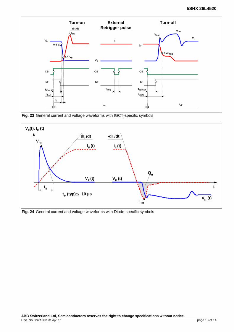
Fig. 23 General current and voltage waveforms with IGCT-specific symbols
Fig. 24 General current and voltage waveforms with Diode-specific symbols
IT
VDSP
VDM
VD
0.4 ITGQ
Turn-off
td(off)
CS
SF
td(off) SF
CS
tr
IT
ITM
dIT/dt
0.9 VD
0.1 VD
VD
Turn-on
td(on) SF
td(on)
SF
External
Retrigger pulse
CS
tretrig
SF
VD
ton toff
VFR
dIF/dt
IF
(t)IF
(t)
VF
(t)
tfr
tfr (typ) 10 µs
Qrr
IRM
-dIF/dt
VF(t), I
F (t)
VF (t)
VR (t)
t
5SHX 26L4520
ABB Switzerland Ltd, Semiconductors reserves the right to change specifications without notice.
ABB Switzerland Ltd Doc. No. 5SYA1251-01 Apr. 16 Semiconductors Fabrikstrasse 3 CH-5600 Lenzburg, Switzerland Telephone +41 (0)58 586 1419 Fax +41 (0)58 586 1306 Email [email protected] Internet www.abb.com/semiconductors
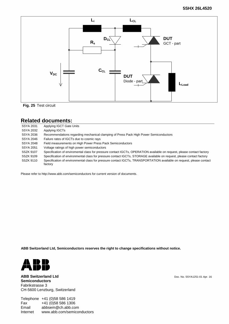
Fig. 25 Test circuit
Related documents: 5SYA 2031 Applying IGCT Gate Units
5SYA 2032 Applying IGCTs
5SYA 2036 Recommendations regarding mechanical clamping of Press Pack High Power Semiconductors
5SYA 2046 Failure rates of IGCTs due to cosmic rays
5SYA 2048 Field measurements on High Power Press Pack Semiconductors
5SYA 2051 Voltage ratings of high power semiconductors
5SZK 9107 Specification of enviromental class for pressure contact IGCTs, OPERATION available on request, please contact factory
5SZK 9109 Specification of environmental class for pressure contact IGCTs, STORAGE available on request, please contact factory
5SZK 9110 Specification of environmental class for pressure contact IGCTs, TRANSPORTATION available on request, please contact factory
Please refer to http://www.abb.com/semiconductors for current version of documents.
LCLLi
Rs
DUTGCT - part
LLoad
DUTDiode - part
CCLVDC
DCL