Embed Size (px)
Citation preview
MOTOROLA.COM/SEMICONDUCTORS
M68HC08Microcontrollers
DRM055/DRev. 01/2004
High Data RateWireless USBOptical MouseSolution Using theMC68HC908QY4and MC68HC908JB12
Designer ReferenceManual
Fre
esc
ale
Se
mic
on
du
cto
r, I
Freescale Semiconductor, Inc.
For More Information On This Product, Go to: www.freescale.com
nc
...

Fre
esc
ale
Se
mic
on
du
cto
r, I
Freescale Semiconductor, Inc.
For More Information On This Product, Go to: www.freescale.com
nc
...

High Data Rate Wireless USB Optical Mouse Solution DRM055
MOTOROLA 3
Motorola and the Stylized M Logo are registered trademarks of Motorola, Inc.DigitalDNA is a trademark of Motorola, Inc.This product incorporates SuperFlash® technology licensed from SST.All brand names and product names appearing in this document are registered trademarks or trademarks of their respective holders. © Motorola, Inc., 2004
High Data Rate Wireless USB Optical Mouse Solution Using the MC68HC908QY4 and MC68HC908JB12 Designer Reference Manual
by: Dennis Lui Ernest Chan Applications Engineering Motorola Microcontroller Division Hong Kong
To provide the most up-to-date information, the revision of our documents on the World Wide Web will be the most current. Your printed copy may be an earlier revision. To verify you have the latest information available, refer to:
http://motorola.com/semiconductors
Fre
esc
ale
Se
mic
on
du
cto
r, I
Freescale Semiconductor, Inc.
For More Information On This Product, Go to: www.freescale.com
nc
...

DRM055 High Data Rate Wireless USB Optical Mouse Solution
4 Revision History MOTOROLA
Revision History
Revision History
DateRevision
LevelDescription
PageNumber(s)
January, 2004
N/A Initial release N/A
Fre
esc
ale
Se
mic
on
du
cto
r, I
Freescale Semiconductor, Inc.
For More Information On This Product, Go to: www.freescale.com
nc
...
High Data Rate Wireless USB Optical Mouse Solution DRM055
MOTOROLA Table of Contents 5
Designer Reference Manual — DRM055
Table of Contents
Section 1. System Overview1.1 Introduction . . . . . . . . . . . . . . . . . . . . . . . . . . . . . . . . . . . . . . . . . . . . . 9
1.2 Features . . . . . . . . . . . . . . . . . . . . . . . . . . . . . . . . . . . . . . . . . . . . . . 10
1.3 System Overview . . . . . . . . . . . . . . . . . . . . . . . . . . . . . . . . . . . . . . . 10
1.4 Transmitter and Receiver . . . . . . . . . . . . . . . . . . . . . . . . . . . . . . . . . 11
Section 2. RF Front End2.1 Introduction . . . . . . . . . . . . . . . . . . . . . . . . . . . . . . . . . . . . . . . . . . . . 13
2.2 Functional Description . . . . . . . . . . . . . . . . . . . . . . . . . . . . . . . . . . . 13
2.3 RF Transmitter . . . . . . . . . . . . . . . . . . . . . . . . . . . . . . . . . . . . . . . . . 13
2.4 RF Receiver . . . . . . . . . . . . . . . . . . . . . . . . . . . . . . . . . . . . . . . . . . . 14
2.5 PCB Layout Guidelines. . . . . . . . . . . . . . . . . . . . . . . . . . . . . . . . . . . 14
Section 3. Universal Serial Bus (USB) Overview3.1 Introduction . . . . . . . . . . . . . . . . . . . . . . . . . . . . . . . . . . . . . . . . . . . . 15
3.2 JB12 USB Module . . . . . . . . . . . . . . . . . . . . . . . . . . . . . . . . . . . . . . 153.2.1 USB Module Description. . . . . . . . . . . . . . . . . . . . . . . . . . . . . . . 163.2.2 USB Connection . . . . . . . . . . . . . . . . . . . . . . . . . . . . . . . . . . . . . 173.2.3 USB Protocol . . . . . . . . . . . . . . . . . . . . . . . . . . . . . . . . . . . . . . . 17
Section 4. Optical Mouse Transmitter4.1 Introduction . . . . . . . . . . . . . . . . . . . . . . . . . . . . . . . . . . . . . . . . . . . . 19
4.2 System Overview . . . . . . . . . . . . . . . . . . . . . . . . . . . . . . . . . . . . . . . 194.2.1 QY4 Microcontroller . . . . . . . . . . . . . . . . . . . . . . . . . . . . . . . . . . 204.2.2 Optical Mouse Sensor . . . . . . . . . . . . . . . . . . . . . . . . . . . . . . . . 20
Section 5. Mouse Transmitter Firmware5.1 Firmware Structure . . . . . . . . . . . . . . . . . . . . . . . . . . . . . . . . . . . . . . 21
5.2 Power Management . . . . . . . . . . . . . . . . . . . . . . . . . . . . . . . . . . . . . 22
5.3 Data Packet Format . . . . . . . . . . . . . . . . . . . . . . . . . . . . . . . . . . . . . 235.3.1 Coding Method . . . . . . . . . . . . . . . . . . . . . . . . . . . . . . . . . . . . . . 235.3.2 Packet Types . . . . . . . . . . . . . . . . . . . . . . . . . . . . . . . . . . . . . . . 235.3.3 Button Status and Z Displacement Packet . . . . . . . . . . . . . . . . . 245.3.4 X-Y Displacements Packet . . . . . . . . . . . . . . . . . . . . . . . . . . . . . 25
Fre
esc
ale
Se
mic
on
du
cto
r, I
Freescale Semiconductor, Inc.
For More Information On This Product, Go to: www.freescale.com
nc
...
DRM055 High Data Rate Wireless USB Optical Mouse Solution
6 Table of Contents MOTOROLA
Table of Contents
Section 6. Universal Serial Bus (USB) Receiver6.1 Introduction . . . . . . . . . . . . . . . . . . . . . . . . . . . . . . . . . . . . . . . . . . . . 27
6.2 System Overview . . . . . . . . . . . . . . . . . . . . . . . . . . . . . . . . . . . . . . . 28
Section 7. Receiver Firmware7.1 Firmware Structure . . . . . . . . . . . . . . . . . . . . . . . . . . . . . . . . . . . . . . 29
7.2 USB Report. . . . . . . . . . . . . . . . . . . . . . . . . . . . . . . . . . . . . . . . . . . . 35
7.3 Remote Wakeup . . . . . . . . . . . . . . . . . . . . . . . . . . . . . . . . . . . . . . . . 357.3.1 Wakeup Detection Mechanism . . . . . . . . . . . . . . . . . . . . . . . . . . 357.3.2 Power Consideration . . . . . . . . . . . . . . . . . . . . . . . . . . . . . . . . . 37
7.4 ID Updating Process. . . . . . . . . . . . . . . . . . . . . . . . . . . . . . . . . . . . . 37
Section 8. Testing and Customization8.1 Testing . . . . . . . . . . . . . . . . . . . . . . . . . . . . . . . . . . . . . . . . . . . . . . . 39
8.2 Hardware Customization . . . . . . . . . . . . . . . . . . . . . . . . . . . . . . . . . 398.2.1 Optical Mouse Transmitter . . . . . . . . . . . . . . . . . . . . . . . . . . . . . 398.2.2 RF Circuitry . . . . . . . . . . . . . . . . . . . . . . . . . . . . . . . . . . . . . . . . . 41
8.3 Firmware Customization . . . . . . . . . . . . . . . . . . . . . . . . . . . . . . . . . . 428.3.1 Mouse Transmitter . . . . . . . . . . . . . . . . . . . . . . . . . . . . . . . . . . . 428.3.2 Receiver . . . . . . . . . . . . . . . . . . . . . . . . . . . . . . . . . . . . . . . . . . . 42
Fre
esc
ale
Se
mic
on
du
cto
r, I
Freescale Semiconductor, Inc.
For More Information On This Product, Go to: www.freescale.com
nc
...
High Data Rate Wireless USB Optical Mouse Solution DRM055
MOTOROLA List of Figures and Tables 7
Designer Reference Manual — DRM055
List of Figures and Tables
Figure Title Page
1-1 System Block Diagram . . . . . . . . . . . . . . . . . . . . . . . . . . . . . . . . . . 11
3-1 USB Block Diagram . . . . . . . . . . . . . . . . . . . . . . . . . . . . . . . . . . . . 163-2 USB Connection. . . . . . . . . . . . . . . . . . . . . . . . . . . . . . . . . . . . . . . 173-3 USB Packet Types . . . . . . . . . . . . . . . . . . . . . . . . . . . . . . . . . . . . . 18
4-1 Transmitter Block Diagram. . . . . . . . . . . . . . . . . . . . . . . . . . . . . . . 20
5-1 Firmware Structure. . . . . . . . . . . . . . . . . . . . . . . . . . . . . . . . . . . . . 215-2 Power Management . . . . . . . . . . . . . . . . . . . . . . . . . . . . . . . . . . . . 225-3 Manchester Coding . . . . . . . . . . . . . . . . . . . . . . . . . . . . . . . . . . . . 235-4 Packet Format for Button and Z Displacement . . . . . . . . . . . . . . . 245-5 Start Field . . . . . . . . . . . . . . . . . . . . . . . . . . . . . . . . . . . . . . . . . . . . 245-6 Button Status Byte . . . . . . . . . . . . . . . . . . . . . . . . . . . . . . . . . . . . . 245-7 Z Displacement or ID Byte . . . . . . . . . . . . . . . . . . . . . . . . . . . . . . . 245-8 Checksum Byte . . . . . . . . . . . . . . . . . . . . . . . . . . . . . . . . . . . . . . . 245-9 Packet Format for X-Y Displacements . . . . . . . . . . . . . . . . . . . . . . 255-10 Start Field for X-Y Displacement Packet . . . . . . . . . . . . . . . . . . . . 25
6-1 USB Receiver. . . . . . . . . . . . . . . . . . . . . . . . . . . . . . . . . . . . . . . . . 27
7-1 Firmware Flow . . . . . . . . . . . . . . . . . . . . . . . . . . . . . . . . . . . . . . . . 307-2 USB Interrupt Routine . . . . . . . . . . . . . . . . . . . . . . . . . . . . . . . . . . 317-3 Setup Routine. . . . . . . . . . . . . . . . . . . . . . . . . . . . . . . . . . . . . . . . . 327-4 OUT EP0 Handler . . . . . . . . . . . . . . . . . . . . . . . . . . . . . . . . . . . . . 327-5 IN EP0 Handler . . . . . . . . . . . . . . . . . . . . . . . . . . . . . . . . . . . . . . . 337-6 Timer Capture Interrupt For Receiver . . . . . . . . . . . . . . . . . . . . . . 347-7 Timing Parameters for Packet Detection . . . . . . . . . . . . . . . . . . . . 367-8 Detection of Valid Wakeup Packets . . . . . . . . . . . . . . . . . . . . . . . . 367-9 JB12 Rejecting Packet-Like Noise
to Prevent False Wakeup . . . . . . . . . . . . . . . . . . . . . . . . . . . . . 37
8-1 USB Report for JB12 to Host for the Test Setup . . . . . . . . . . . . . . 408-2 Loop Antenna Impedance . . . . . . . . . . . . . . . . . . . . . . . . . . . . . . . 41
Fre
esc
ale
Se
mic
on
du
cto
r, I
Freescale Semiconductor, Inc.
For More Information On This Product, Go to: www.freescale.com
nc
...
DRM055 High Data Rate Wireless USB Optical Mouse Solution
8 List of Figures and Tables MOTOROLA
List of Figures and Tables
Table Title Page
7-1 Interface 1 Mouse Input Report . . . . . . . . . . . . . . . . . . . . . . . . . . . 35
8-1 Tx Matching Examples . . . . . . . . . . . . . . . . . . . . . . . . . . . . . . . . . . 418-2 Rx Matching Examples. . . . . . . . . . . . . . . . . . . . . . . . . . . . . . . . . . 41
Fre
esc
ale
Se
mic
on
du
cto
r, I
Freescale Semiconductor, Inc.
For More Information On This Product, Go to: www.freescale.com
nc
...
High Data Rate Wireless USB Optical Mouse Solution DRM055
MOTOROLA System Overview 9
Designer Reference Manual — DRM055
Section 1. System Overview
1.1 Introduction
This manual describes a reference design for a high data rate wireless universal serial bus (USB) optical mouse solution by using the MC68HC908QY4 and the MC68HC908JB12.
Because of the lower cost, adoption of wireless PC peripherals has been fast paced. Consumers are quickly recognizing the advantages of using wireless PC peripherals, which include portability and placement flexibility. However, there are two major performance issues in general 27-MHz wireless platforms. These issues affect wireless mouse applications in particular.
1. The mouse cursor motion tracking speed is slow
2. There is a long legacy time in response to an end-user action
These issues can be resolved by implementation of a new high-speed transmission link. The tracking speed of the high data rate wireless mouse is almost doubled and the response time is reduced by half. The performance is even compatible to a corded mouse in terms of data report rates uploaded to the PC host from the peripheral device. From the end users point of view, the overall movement of the mouse can be fully cached up and reflected on the computer screen without any noticeable delay in cursor response.
The following reference materials are available at:http://motorola.com/semiconductors
• Schematic diagram
• PCB layout
• PCB Gerber
• Bill of materials
• Source code
Fre
esc
ale
Se
mic
on
du
cto
r, I
Freescale Semiconductor, Inc.
For More Information On This Product, Go to: www.freescale.com
nc
...

DRM055 High Data Rate Wireless USB Optical Mouse Solution
10 System Overview MOTOROLA
System Overview
1.2 Features
Main features of the mouse include:
• A high data rate 27-MHz RF link
• Windows® 98, Windows 2000, and Windows XP compatibility
• User identity code to avoid conflict with other devices
• USB 2.0 low-speed compliance
• 4.8 kbps transmission data rate
• 2 meter communication distance
• 3361 compatible device for RF receiver design
1.3 System Overview
The system consists of:
• A high data rate wireless optical mouse using the MC68HC908QY4 (hereafter referred as QY4)
• A USB receiver using the MC68HC908JB12 (hereafter referred as JB12).
The QY4 was chosen as the mouse transmitter because it includes:
• An internal oscillator circuit
• An auto wakeup function
The JB12 is suitable for this high data rate wireless optical mouse application because it has:
• 12-K FLASH memory
• 6-MHz bus processing power
• USB function
• An enhanced timer capture module
NOTE: The traditional track-ball type X-Y detection method was replaced by the advance optical navigation technology that serves as a non-mechanical motion estimation.
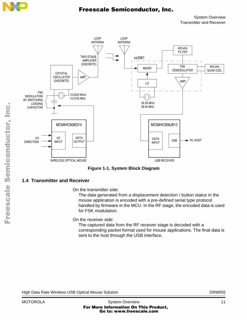
A block diagram of the system is shown in Figure 1-1.
Windows is a registered trademark of Microsoft Corporation in the United States and other countries.
Fre
esc
ale
Se
mic
on
du
cto
r, I
Freescale Semiconductor, Inc.
For More Information On This Product, Go to: www.freescale.com
nc
...
System OverviewTransmitter and Receiver
High Data Rate Wireless USB Optical Mouse Solution DRM055
MOTOROLA System Overview 11
Figure 1-1. System Block Diagram
1.4 Transmitter and Receiver
On the transmitter side:The data generated from a displacement detection / button status in the mouse application is encoded with a pre-defined serial type protocol handled by firmware in the MCU. In the RF stage, the encoded data is used for FSK modulation.
On the receiver side:The captured data from the RF receiver stage is decoded with a corresponding packet format used for mouse applications. The final data is sent to the host through the USB interface.
455 kHzQUAD COIL
MIXER FSKDEMODULATOR
LOAMP
xx3361
455 kHzFILTER
LOOPANTENNA
26.59 MHz/26.64 MHz
MC68HC908JB12
USB PC HOST
USB RECEIVER
MC68HC908QY4
I/OINPUT
DATAOUTPUT
WIRELESS OPTICAL MOUSE
DATAINPUT
I/ODIRECTION
LOOPANTENNA
TWO-STAGEAMPLIFIER
(DISCRETE)
AMPCRYSTAL
OSCILLATOR(DISCRETE)
13.5225 MHz/13.5725 MHz
FSKMODULATION
BY SWITCHINGLOADING
CAPACITOR
Fre
esc
ale
Se
mic
on
du
cto
r, I
Freescale Semiconductor, Inc.
For More Information On This Product, Go to: www.freescale.com
nc
...

DRM055 High Data Rate Wireless USB Optical Mouse Solution
12 System Overview MOTOROLA
System Overview
Fre
esc
ale
Se
mic
on
du
cto
r, I
Freescale Semiconductor, Inc.
For More Information On This Product, Go to: www.freescale.com
nc
...
High Data Rate Wireless USB Optical Mouse Solution DRM055
MOTOROLA RF Front End 13
Designer Reference Manual — DRM055
Section 2. RF Front End
2.1 Introduction
A high data rate 27-MHz RF link is designed as the wireless communication media for this application. The RF frequency is determined by the crystal frequency used at the oscillator circuit stage and there are two selectable channels for transmission. The transmission data rate is 4.8 kbps.
2.2 Functional Description
The high-frequency carrier signal on the transmitter side is modulated by the digital encoded data from the QY4 using a FSK modulation scheme. The modulated RF signal is propagated through free-air space and received by an integrated chip, the 3361, on the receiver side which includes all mixer, local oscillator, and demodulator circuits. The demodulated data output is received by the JB12 for decoding and processing. The data will then be converted to the USB mouse report format and sent to the host.
2.3 RF Transmitter
The RF transmitter consists of three parts:
• The crystal type oscillator
• The FSK modulation switching circuit
• The RF amplifier
The crystal oscillator works with a crystal frequency at half of the target channel frequency and the second harmonic frequency is filtered out by the RF amplifier together with a high Q-factor antenna. For example, a 13.5225-MHz crystal is used for a frequency channel at 27.045-MHz.
The FSK modulation is achieved by changing the loading capacitance at the crystal with a transistor switching circuit controlled by the encoding data generated from the MCU. The maximum data rate for a particular FSK transmission is limited by the RF bandwidth of the system and controlled by the frequency deviation which represents the logic “0” and logic “1” data. In general, the frequency deviation should be adjusted proportionally to the change on the required transmission data rate. Higher data rates require more bandwidth / frequency deviation. The frequency deviation for this 4.8-kbps data
Fre
esc
ale
Se
mic
on
du
cto
r, I
Freescale Semiconductor, Inc.
For More Information On This Product, Go to: www.freescale.com
nc
...
DRM055 High Data Rate Wireless USB Optical Mouse Solution
14 RF Front End MOTOROLA
RF Front End
rate wireless mouse application is increased from ±2.5 kHz to ±4.5 kHz which is controlled by the crystal characteristics.
The gain of the RF amplifier in the final stage should be adjusted to compensate the gain loss at the oscillator stage with extend bandwidth operation. Two stages of RF amplifier are used in this reference design to maintain the performance in communication distance.
2.4 RF Receiver
The RF receiver is implemented by using a single-chip solution (3361 compatible part) which includes:
• A frequency downward conversion mixer
• A local oscillator circuit
• A baseband FSK quadrature demodulation unit
The RF input signal from the antenna, is frequency down converted into an IF signal at 455 kHz by the mixer and oscillator circuits. The IF frequency value is equal to the RF input frequency plus or minus the LO input frequency. The higher frequency components should be filtered out by using a passive IF filter. The bandwidth should be increased from 15 kHz to 20 kHz to match the data rate change on the transmitter side.
However, the image frequency component would not be filtered out by the IF filter. This should be considered in the PCB layout in order to prevent any noise component at image frequency to be injected into the mixer input. An example of this would be a noise pattern generated from the MCU.
The frequency used for a 3361 mixer local oscillator is selected by the crystal connected at the oscillator base input pin. There are two frequency channels that can be selected to match the transmitter channel.
2.5 PCB Layout Guidelines
Care should be taken in PCB layout in order to avoid any noise generated from MCU coupling into the RF stage. For example:
• The power supply traces used for digital and analog circuit blocks should be separated.
• The location of decoupling capacitors should be as close as possible to device's supply input pins (VDD/VSS or VCC/GND).
• The VDD to VSS ground loop area should be reduced to minimize the magnetic coupling effect.
• The PCB trace loop formed by any input/output (I/O) signal pin should be kept to a minimum.
• The RF receiver uses a loop antenna formed by using a PCB trace line.
Fre
esc
ale
Se
mic
on
du
cto
r, I
Freescale Semiconductor, Inc.
For More Information On This Product, Go to: www.freescale.com
nc
...
High Data Rate Wireless USB Optical Mouse Solution DRM055
MOTOROLA Universal Serial Bus (USB) Overview 15
Designer Reference Manual — DRM055
Section 3. Universal Serial Bus (USB) Overview
3.1 Introduction
The universal serial bus (USB) is an industry-standard extension to PC architecture providing a low-cost plug-and-play solution for PC peripheral devices. It is a serial data link with a high data-transfer rate and device-control capability. Peripheral USB devices can be configured automatically when connected to a host because the USB software driver is mapped and loaded in the operating system (OS) according to the peripheral device class.
The USB driver knows how to communicate with the devices and the USB devices will report their attributes (using a specific report format called descriptor) to the host during device configuration. The descriptor is a data structure with a defined format that describes the device’s capabilities and resource requirements.
For more detailed information regarding the descriptor format, please refer to the Universal Serial Bus Specification Revision 2.0 at:
http://www.usb.org/developers/docs
3.2 JB12 USB Module
Features of the JB12 USB module include:
• Universal Serial Bus Specification 2.0 low-speed functions
• 1.5-Mbps data rate
• On-chip 3.3 -V regulator
• Endpoint 0 with 8-byte transmit buffer and 8-byte receive buffer
• Endpoint 1 with 8-byte transmit buffer
• Endpoint 2 with 8-byte transmit buffer and 8-byte receive buffer
• USB data control logic
• USB reset options
• Suspend and resume operations with remote wakeup support
• USB-generated interrupts
• STALL, NAK, and ACK handshake generation
Fre
esc
ale
Se
mic
on
du
cto
r, I
Freescale Semiconductor, Inc.
For More Information On This Product, Go to: www.freescale.com
nc
...
DRM055 High Data Rate Wireless USB Optical Mouse Solution
16 Universal Serial Bus (USB) Overview MOTOROLA
Universal Serial Bus (USB) Overview
3.2.1 USB Module Description
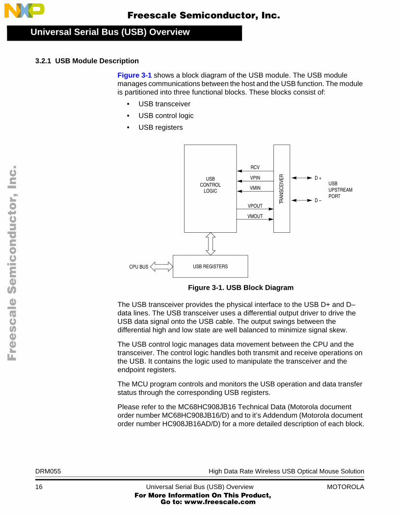
Figure 3-1 shows a block diagram of the USB module. The USB module manages communications between the host and the USB function. The module is partitioned into three functional blocks. These blocks consist of:
• USB transceiver
• USB control logic
• USB registers
Figure 3-1. USB Block Diagram
The USB transceiver provides the physical interface to the USB D+ and D– data lines. The USB transceiver uses a differential output driver to drive the USB data signal onto the USB cable. The output swings between the differential high and low state are well balanced to minimize signal skew.
The USB control logic manages data movement between the CPU and the transceiver. The control logic handles both transmit and receive operations on the USB. It contains the logic used to manipulate the transceiver and the endpoint registers.
The MCU program controls and monitors the USB operation and data transfer status through the corresponding USB registers.
Please refer to the MC68HC908JB16 Technical Data (Motorola document order number MC68HC908JB16/D) and to it’s Addendum (Motorola document order number HC908JB16AD/D) for a more detailed description of each block.
D +
D –TRAN
SCEI
VER
RCV
VPIN
VMIN
VPOUT
VMOUT
CPU BUS USB REGISTERS
USBUPSTREAMPORT
USBCONTROL
LOGIC
Fre
esc
ale
Se
mic
on
du
cto
r, I
Freescale Semiconductor, Inc.
For More Information On This Product, Go to: www.freescale.com
nc
...
Universal Serial Bus (USB) OverviewJB12 USB Module
High Data Rate Wireless USB Optical Mouse Solution DRM055
MOTOROLA Universal Serial Bus (USB) Overview 17
3.2.2 USB Connection
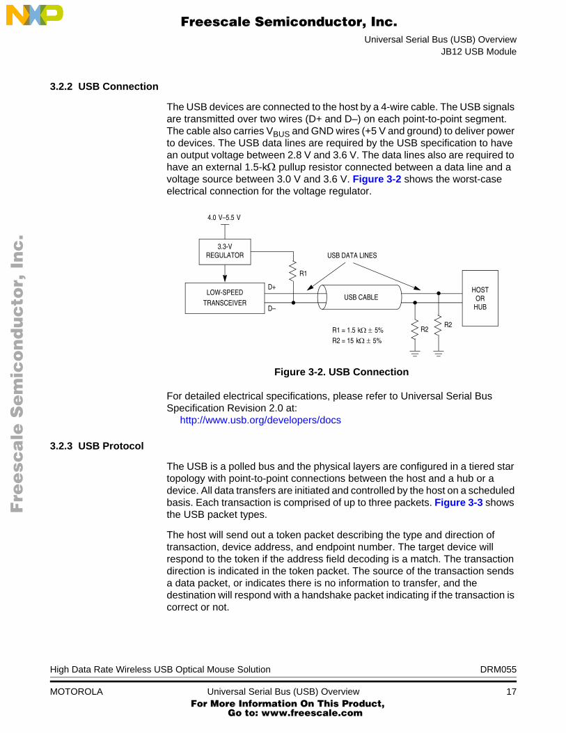
The USB devices are connected to the host by a 4-wire cable. The USB signals are transmitted over two wires (D+ and D–) on each point-to-point segment. The cable also carries VBUS and GND wires (+5 V and ground) to deliver power to devices. The USB data lines are required by the USB specification to have an output voltage between 2.8 V and 3.6 V. The data lines also are required to have an external 1.5-kΩ pullup resistor connected between a data line and a voltage source between 3.0 V and 3.6 V. Figure 3-2 shows the worst-case electrical connection for the voltage regulator.
Figure 3-2. USB Connection
For detailed electrical specifications, please refer to Universal Serial Bus Specification Revision 2.0 at:
http://www.usb.org/developers/docs
3.2.3 USB Protocol
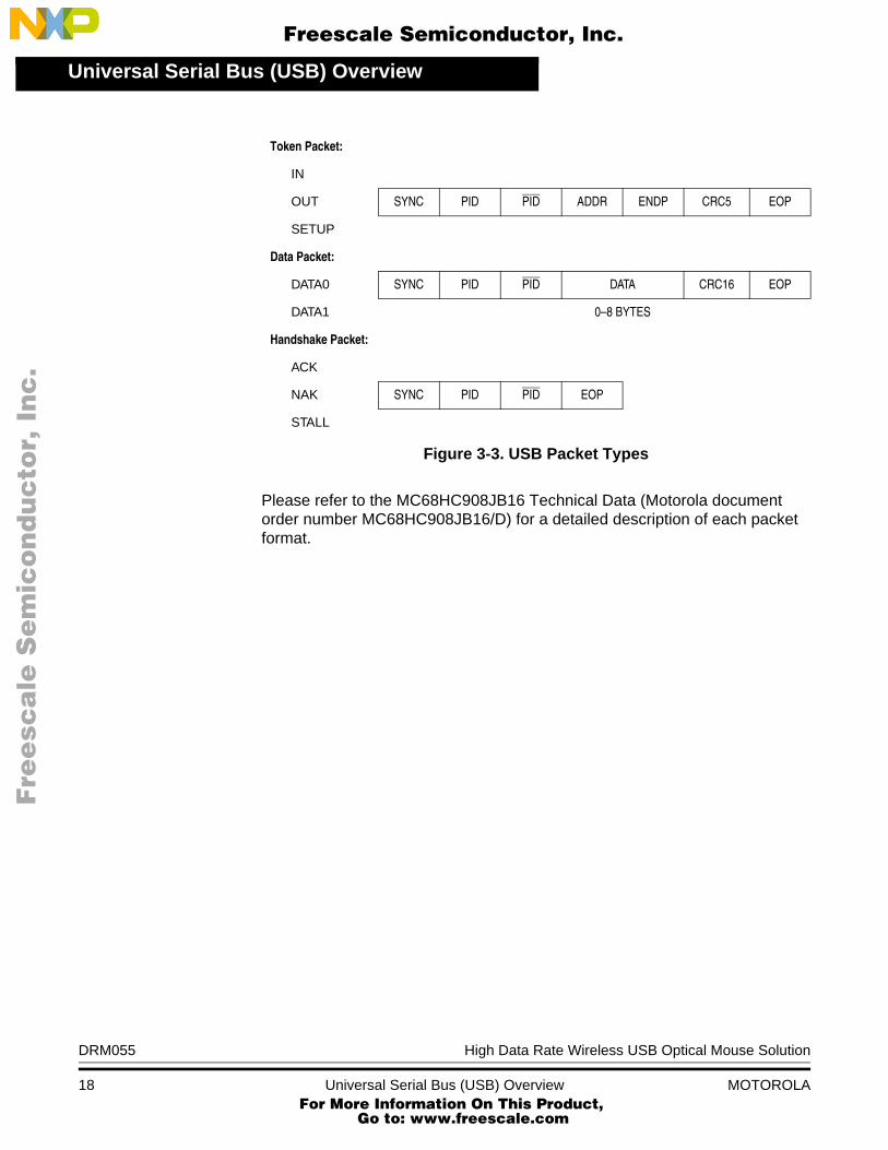
The USB is a polled bus and the physical layers are configured in a tiered star topology with point-to-point connections between the host and a hub or a device. All data transfers are initiated and controlled by the host on a scheduled basis. Each transaction is comprised of up to three packets. Figure 3-3 shows the USB packet types.
The host will send out a token packet describing the type and direction of transaction, device address, and endpoint number. The target device will respond to the token if the address field decoding is a match. The transaction direction is indicated in the token packet. The source of the transaction sends a data packet, or indicates there is no information to transfer, and the destination will respond with a handshake packet indicating if the transaction is correct or not.
R1
D+
D–
USB CABLELOW-SPEED
TRANSCEIVER
R2R2
3.3-VREGULATOR
4.0 V–5.5 V
USB DATA LINES
R1 = 1.5 kΩ ± 5%R2 = 15 kΩ ± 5%
HOSTOR
HUB
Fre
esc
ale
Se
mic
on
du
cto
r, I
Freescale Semiconductor, Inc.
For More Information On This Product, Go to: www.freescale.com
nc
...
DRM055 High Data Rate Wireless USB Optical Mouse Solution
18 Universal Serial Bus (USB) Overview MOTOROLA
Universal Serial Bus (USB) Overview
Please refer to the MC68HC908JB16 Technical Data (Motorola document order number MC68HC908JB16/D) for a detailed description of each packet format.
Token Packet:
IN
OUT SYNC PID PID ADDR ENDP CRC5 EOP
SETUP
Data Packet:
DATA0 SYNC PID PID DATA CRC16 EOP
DATA1 0–8 BYTES
Handshake Packet:
ACK
NAK SYNC PID PID EOP
STALL
Figure 3-3. USB Packet Types
Fre
esc
ale
Se
mic
on
du
cto
r, I
Freescale Semiconductor, Inc.
For More Information On This Product, Go to: www.freescale.com
nc
...
High Data Rate Wireless USB Optical Mouse Solution DRM055
MOTOROLA Optical Mouse Transmitter 19
Designer Reference Manual — DRM055
Section 4. Optical Mouse Transmitter
4.1 Introduction
The features of the high data rate wireless USB optical mouse solution include an internal oscillator circuit which can generate a clock of 12.8 MHz with no external components needed. The auto wakeup module generates a periodic interrupt during stop mode to wake the part up without requiring an external signal. These features make the QY4 MCU suited for wireless optical mouse applications.
The main features of the reference design include:
• 27-MHz RF transmitter
• 4.8-kbps transmission data rate
• 800-DPI resolution
• Smart power management
4.2 System Overview
The mouse transmitter consists of:
• The QY4
• The Agilent optical mouse sensor (ADNS-2030)
• The RF front end
Refer to Figure 4-1 for a block diagram of the system.
NOTE: RF data is transmitted by means of setting and clearing the RF_Data and the RF_Off pin.
Fre
esc
ale
Se
mic
on
du
cto
r, I
Freescale Semiconductor, Inc.
For More Information On This Product, Go to: www.freescale.com
nc
...
DRM055 High Data Rate Wireless USB Optical Mouse Solution
20 Optical Mouse Transmitter MOTOROLA
Optical Mouse Transmitter
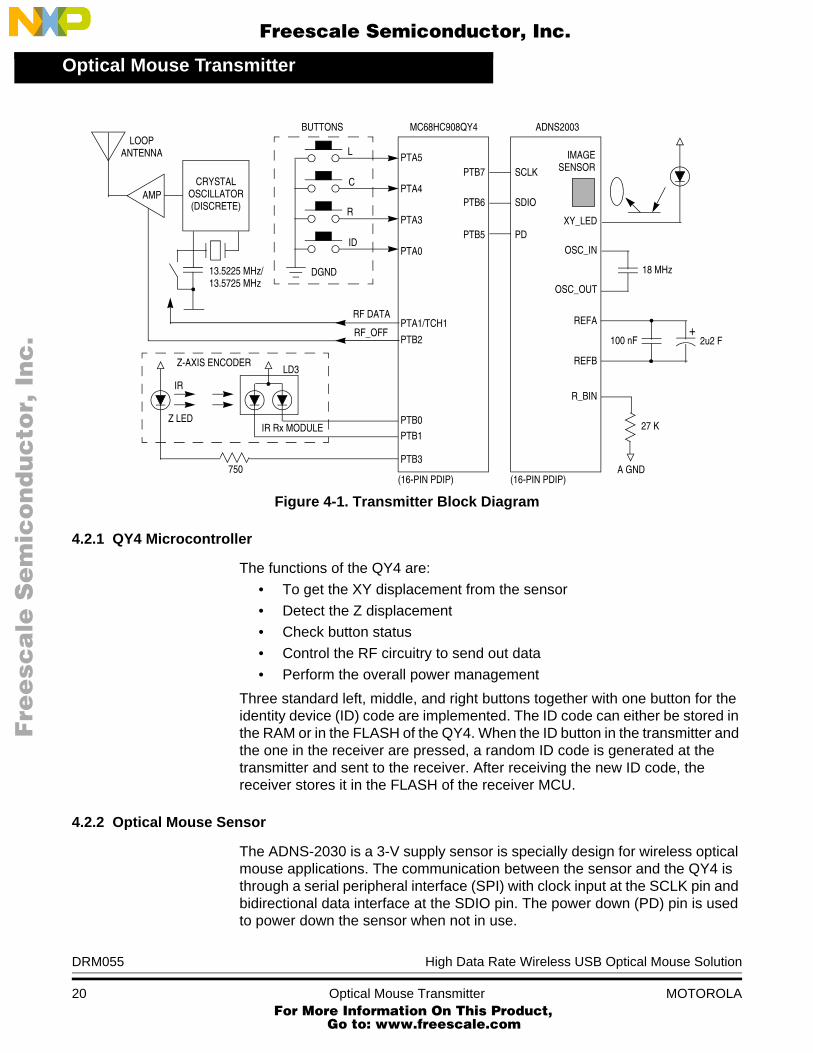
Figure 4-1. Transmitter Block Diagram
4.2.1 QY4 Microcontroller
The functions of the QY4 are:
• To get the XY displacement from the sensor
• Detect the Z displacement
• Check button status
• Control the RF circuitry to send out data
• Perform the overall power management
Three standard left, middle, and right buttons together with one button for the identity device (ID) code are implemented. The ID code can either be stored in the RAM or in the FLASH of the QY4. When the ID button in the transmitter and the one in the receiver are pressed, a random ID code is generated at the transmitter and sent to the receiver. After receiving the new ID code, the receiver stores it in the FLASH of the receiver MCU.
4.2.2 Optical Mouse Sensor
The ADNS-2030 is a 3-V supply sensor is specially design for wireless optical mouse applications. The communication between the sensor and the QY4 is through a serial peripheral interface (SPI) with clock input at the SCLK pin and bidirectional data interface at the SDIO pin. The power down (PD) pin is used to power down the sensor when not in use.
AMP
LOOPANTENNA
CRYSTALOSCILLATOR(DISCRETE)
13.5225 MHz/13.5725 MHz
DGND
L
C
R
ID
BUTTONS
PTA5
PTA4
PTA3
PTA0
PTA1/TCH1
PTB2
PTB0
PTB1
PTB3
PTB7
PTB6
PTB5
SCLK
SDIO
PD
RF DATA
RF_OFF
Z-AXIS ENCODER
IR
Z LED
LD3
IR Rx MODULE
MC68HC908QY4
(16-PIN PDIP)
ADNS2003
(16-PIN PDIP)750
IMAGESENSOR
18 MHz
2u2 F
27 K
100 nF
A GND
+
XY_LED
OSC_IN
OSC_OUT
REFA
REFB
R_BIN
Fre
esc
ale
Se
mic
on
du
cto
r, I
Freescale Semiconductor, Inc.
For More Information On This Product, Go to: www.freescale.com
nc
...
High Data Rate Wireless USB Optical Mouse Solution DRM055
MOTOROLA Mouse Transmitter Firmware 21
Designer Reference Manual — DRM055
Section 5. Mouse Transmitter Firmware
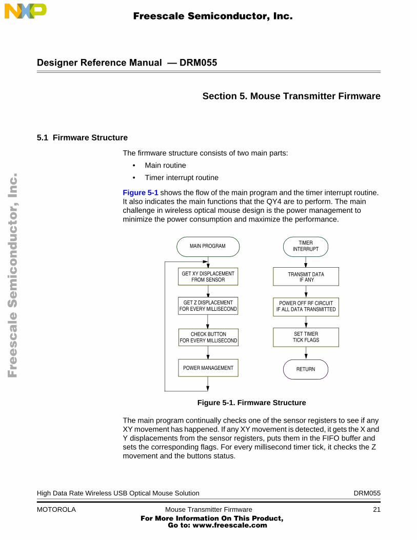
5.1 Firmware Structure
The firmware structure consists of two main parts:
• Main routine
• Timer interrupt routine
Figure 5-1 shows the flow of the main program and the timer interrupt routine. It also indicates the main functions that the QY4 are to perform. The main challenge in wireless optical mouse design is the power management to minimize the power consumption and maximize the performance.
Figure 5-1. Firmware Structure
The main program continually checks one of the sensor registers to see if any XY movement has happened. If any XY movement is detected, it gets the X and Y displacements from the sensor registers, puts them in the FIFO buffer and sets the corresponding flags. For every millisecond timer tick, it checks the Z movement and the buttons status.
MAIN PROGRAM
GET XY DISPLACEMENT
GET Z DISPLACEMENT
TIMER
TRANSMIT DATAIF ANY
SET TIMERTICK FLAGS
RETURN
POWER OFF RF CIRCUITIF ALL DATA TRANSMITTED
FROM SENSOR
CHECK BUTTON
POWER MANAGEMENT
FOR EVERY MILLISECOND
FOR EVERY MILLISECOND
INTERRUPT
Fre
esc
ale
Se
mic
on
du
cto
r, I
Freescale Semiconductor, Inc.
For More Information On This Product, Go to: www.freescale.com
nc
...
DRM055 High Data Rate Wireless USB Optical Mouse Solution
22 Mouse Transmitter Firmware MOTOROLA
Mouse Transmitter Firmware
A timer interrupt is set for every 104 µs which is the base time for the 4.8-kHz data rate transmission. By configuring the timer to output compare mode, the RF_Data output pin can be set, cleared, or toggled for every 104 µs. The timer interrupt routine determines whether to set or clear the RF_Data pin at the next interrupt time. It also determines what the current RF_Off pin status should be.
5.2 Power Management
Power management plays a very important role in the wireless optical mouse solution.
Figure 5-2. Power Management
Figure 5-2 shows the power management flow. There are three defined stages:
• Power saving
• High current
• Sleep
After power up, the mouse is put in the power saving stage. In this stage, the sensor is only turned on every 20 milliseconds to see if any XY movement happened. The Z movement and buttons are sensed every millisecond.
If no activity happens for 90 seconds, it enters sleep stage. In this stage, the QY4 is put in stop mode and will wake up every 200 milliseconds to monitor any
SENSOR AND ZLED TURNED ONFOR EVERY 200 MILLISECONDS
(EVERY 500 MILLISECONDS IF IN
SLEEP
SLEEP FOR MORE THAN 10 MINUTES)
SENSOR FULLY TURNED ONZLED TURNED ON
FOR EVERY 1 MILLISECOND
HIGH CURRENT
SENSOR TURNED ON EVERY20 MILLISECONDS, ZLED TURNED
ON FOR EVERY 1 MILLISECOND
POWER SAVING(STARTUP)
XY MOVEMENT
XY NO MOVEMENT
Z MOVEMENTOR BUTTON
XYZ NO MOVEMENTAND
NO BUTTON FOR 90 SECONDS
FOR 5 SECONDS
XY MOVEMENT
Fre
esc
ale
Se
mic
on
du
cto
r, I
Freescale Semiconductor, Inc.
For More Information On This Product, Go to: www.freescale.com
nc
...
Mouse Transmitter FirmwareData Packet Format
High Data Rate Wireless USB Optical Mouse Solution DRM055
MOTOROLA Mouse Transmitter Firmware 23
activity. If still no activity happens for 10 minutes, the activities are monitored every 500 milliseconds.
Any XY movement will cause the mouse to enter high current stage. At this stage, the sensor is powered on and XY movement is continually monitored. The Z movement and button activities are still monitored every millisecond. If no XY movement happens for 5 seconds, it then enters power saving stage.
NOTE: Except for the 1 millisecond timer tick, all of the above mentioned timings can be configured by changing their constant values.
5.3 Data Packet Format
A data packet consists of a start field, a data field, and a checksum field.
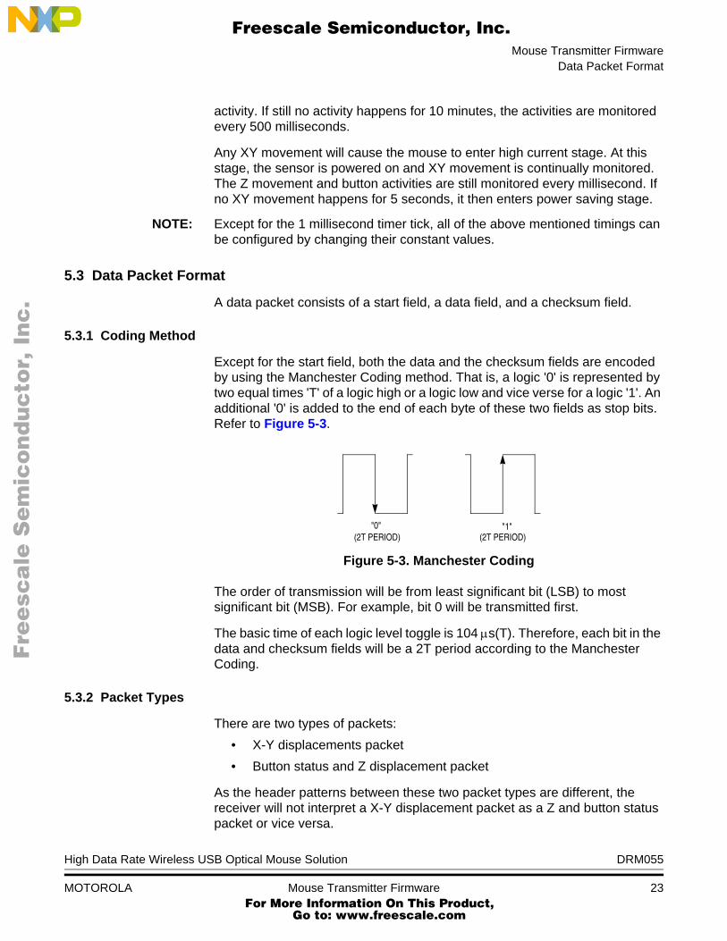
5.3.1 Coding Method
Except for the start field, both the data and the checksum fields are encoded by using the Manchester Coding method. That is, a logic '0' is represented by two equal times 'T' of a logic high or a logic low and vice verse for a logic '1'. An additional '0' is added to the end of each byte of these two fields as stop bits. Refer to Figure 5-3.
Figure 5-3. Manchester Coding
The order of transmission will be from least significant bit (LSB) to most significant bit (MSB). For example, bit 0 will be transmitted first.
The basic time of each logic level toggle is 104 µs(T). Therefore, each bit in the data and checksum fields will be a 2T period according to the Manchester Coding.
5.3.2 Packet Types
There are two types of packets:
• X-Y displacements packet
• Button status and Z displacement packet
As the header patterns between these two packet types are different, the receiver will not interpret a X-Y displacement packet as a Z and button status packet or vice versa.
"0" "1" (2T PERIOD) (2T PERIOD)
Fre
esc
ale
Se
mic
on
du
cto
r, I
Freescale Semiconductor, Inc.
For More Information On This Product, Go to: www.freescale.com
nc
...
DRM055 High Data Rate Wireless USB Optical Mouse Solution
24 Mouse Transmitter Firmware MOTOROLA
Mouse Transmitter Firmware
5.3.3 Button Status and Z Displacement Packet
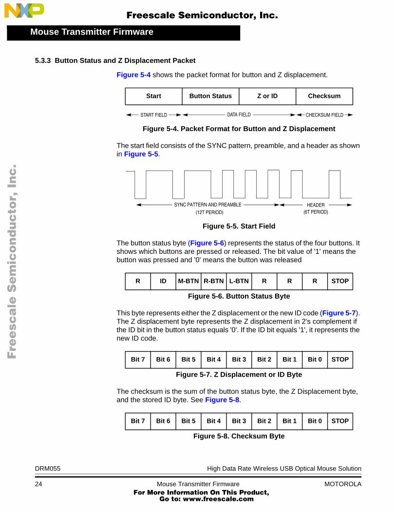
Figure 5-4 shows the packet format for button and Z displacement.
Figure 5-4. Packet Format for Button and Z Displacement
The start field consists of the SYNC pattern, preamble, and a header as shown in Figure 5-5.
Figure 5-5. Start Field
The button status byte (Figure 5-6) represents the status of the four buttons. It shows which buttons are pressed or released. The bit value of '1' means the button was pressed and '0' means the button was released
Figure 5-6. Button Status Byte
This byte represents either the Z displacement or the new ID code (Figure 5-7). The Z displacement byte represents the Z displacement in 2's complement if the ID bit in the button status equals '0'. If the ID bit equals '1', it represents the new ID code.
Figure 5-7. Z Displacement or ID Byte
The checksum is the sum of the button status byte, the Z Displacement byte, and the stored ID byte. See Figure 5-8.
Figure 5-8. Checksum Byte
Start Button Status Z or ID Checksum
R ID M-BTN R-BTN L-BTN R R R STOP
Bit 7 Bit 6 Bit 5 Bit 4 Bit 3 Bit 2 Bit 1 Bit 0 STOP
Bit 7 Bit 6 Bit 5 Bit 4 Bit 3 Bit 2 Bit 1 Bit 0 STOP
START FIELD DATA FIELD CHECKSUM FIELD
HEADER(6T PERIOD)
SYNC PATTERN AND PREAMBLE
(12T PERIOD)
Fre
esc
ale
Se
mic
on
du
cto
r, I
Freescale Semiconductor, Inc.
For More Information On This Product, Go to: www.freescale.com
nc
...

Mouse Transmitter FirmwareData Packet Format
High Data Rate Wireless USB Optical Mouse Solution DRM055
MOTOROLA Mouse Transmitter Firmware 25
5.3.4 X-Y Displacements Packet
Figure 5-9 shows the packet format for X-Y displacements with the start field illustrations in Figure 5-10.
Figure 5-9. Packet Format for X-Y Displacements
Figure 5-10. Start Field for X-Y Displacement Packet
The X or Y displacement is represented in 2's complement and the checksum byte is the sum of the X displacement, the Y displacement, and the stored ID byte.
Start X Displacement Y Displacement Checksum
START FIELD DATA FIELD CHECKSUM FIELD
SYNC PATTERN AND PREAMBLE (12T PERIOD)
HEADER(6T PERIOD)
Fre
esc
ale
Se
mic
on
du
cto
r, I
Freescale Semiconductor, Inc.
For More Information On This Product, Go to: www.freescale.com
nc
...

DRM055 High Data Rate Wireless USB Optical Mouse Solution
26 Mouse Transmitter Firmware MOTOROLA
Mouse Transmitter Firmware
Fre
esc
ale
Se
mic
on
du
cto
r, I
Freescale Semiconductor, Inc.
For More Information On This Product, Go to: www.freescale.com
nc
...

High Data Rate Wireless USB Optical Mouse Solution DRM055
MOTOROLA Universal Serial Bus (USB) Receiver 27
Designer Reference Manual — DRM055
Section 6. Universal Serial Bus (USB) Receiver
6.1 Introduction
The features of the JB12 include a configurable universal serial bus (USB) and PS/2 interface, which makes this MCU suited for personal computer human interface devices (HID) applications, such as mice. The enhanced timer function also allows it to capture and decode data easily, especially for high data rate wireless HID applications. Refer to Figure 6-1.
The main features of the receiver include:
• 27-MHz RF receiver
• Fully USB specification 2.0 low-speed compliant
• Windows 98, 2000, and XP compatible
Figure 6-1. USB Receiver
WAKEUPCIRCUIT
MC68HC908JB12
(SO20)
ICPINTERFACE
PTA0
PTA1
PTA2
PTA3
ID
PCHOST
USB
5 V
1K5
D–D+
GND
VDD
VREG
PTE4
PTE3VSS
RSTOSC2
OSC1
10 M
30 pF
X1
12 MHz
10 nF
30 pF
xx3361
MIXER FSKDEMODULATOR
AMP
455 kHzQUAD COIL
LO
26.59 MHz/26.64 MHz
455 kHzFILTER
RF_DATA
RF_OFFPTE1
PTA4
5 V 1 K
SLEEP
NC
PTC0
IRQ
PTA7–PTA5
Fre
esc
ale
Se
mic
on
du
cto
r, I
Freescale Semiconductor, Inc.
For More Information On This Product, Go to: www.freescale.com
nc
...
DRM055 High Data Rate Wireless USB Optical Mouse Solution
28 Universal Serial Bus (USB) Receiver MOTOROLA
Universal Serial Bus (USB) Receiver
6.2 System Overview
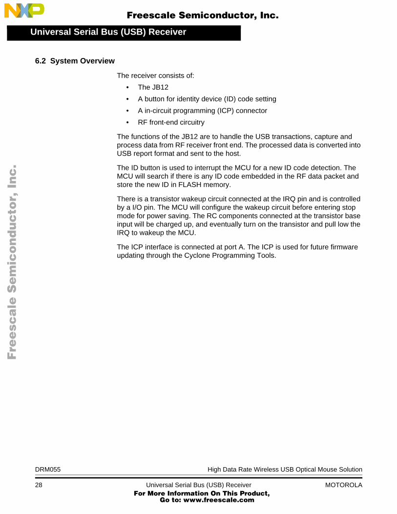
The receiver consists of:
• The JB12
• A button for identity device (ID) code setting
• A in-circuit programming (ICP) connector
• RF front-end circuitry
The functions of the JB12 are to handle the USB transactions, capture and process data from RF receiver front end. The processed data is converted into USB report format and sent to the host.
The ID button is used to interrupt the MCU for a new ID code detection. The MCU will search if there is any ID code embedded in the RF data packet and store the new ID in FLASH memory.
There is a transistor wakeup circuit connected at the IRQ pin and is controlled by a I/O pin. The MCU will configure the wakeup circuit before entering stop mode for power saving. The RC components connected at the transistor base input will be charged up, and eventually turn on the transistor and pull low the IRQ to wakeup the MCU.
The ICP interface is connected at port A. The ICP is used for future firmware updating through the Cyclone Programming Tools.
Fre
esc
ale
Se
mic
on
du
cto
r, I
Freescale Semiconductor, Inc.
For More Information On This Product, Go to: www.freescale.com
nc
...
High Data Rate Wireless USB Optical Mouse Solution DRM055
MOTOROLA Receiver Firmware 29
Designer Reference Manual — DRM055
Section 7. Receiver Firmware
7.1 Firmware Structure
The firmware consists of three main parts:
• Main routine
• Timer interrupt routine to capture and decode mouse data
• USB interrupt routine
The USB routine includes reference codes for both universal serial bus (USB) mouse and keyboard. Thus, it can be a reference on how to implement a composite USB keyboard-mouse device using the JB12.
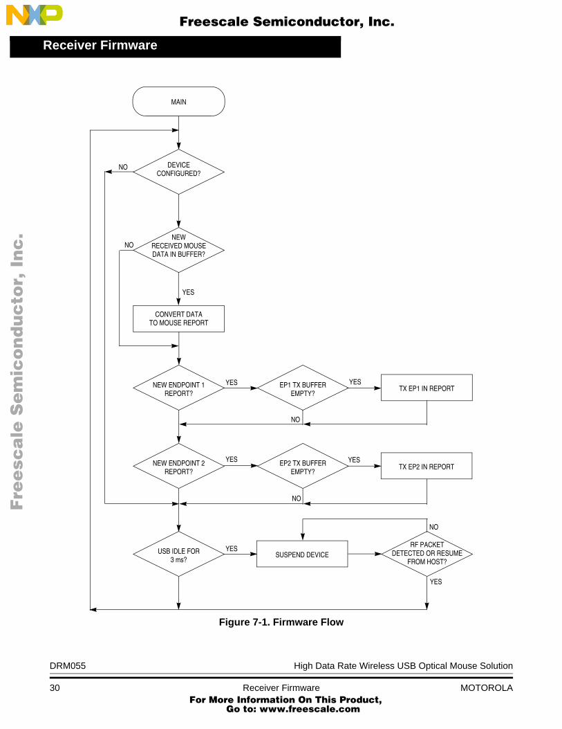
Figure 7-1 shows the flow of the main program for the JB12 receiver. The main routine continually checks to see if there is any valid mouse data in the receiver buffer queue. If there is new data received, the data will be converted to USB report format and sent to the host via the USB endpoints.
Figure 7-2 shows the USB interrupt routines. The USB engine automatically responds to a valid USB token with either ACK, NAK, or STALL, depending on the register settings, and ignores it if it’s invalid. The firmware has to set the registers for the USB engine to give correct response to the token in different stages. The USB interrupt will be executed whenever there is an EOP, resume signal from host, valid data received, or data transmitted. The USB interrupt routine also makes preparation for the next USB transaction and handles any valid command or data received.
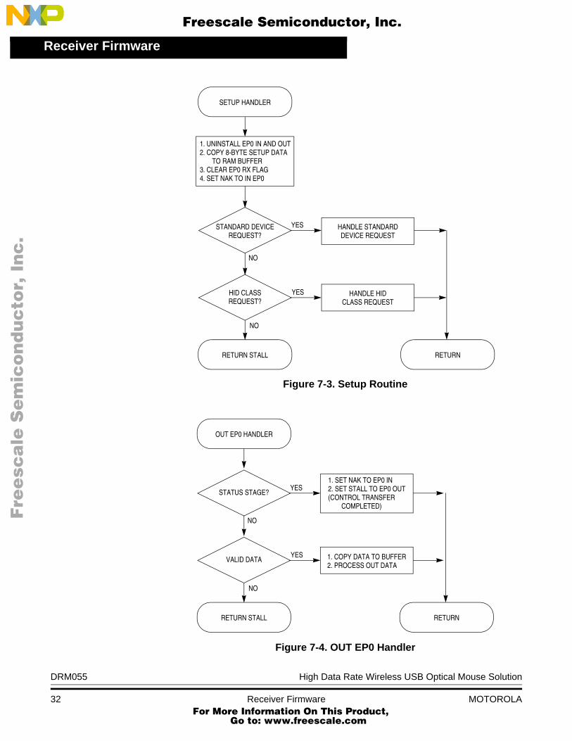
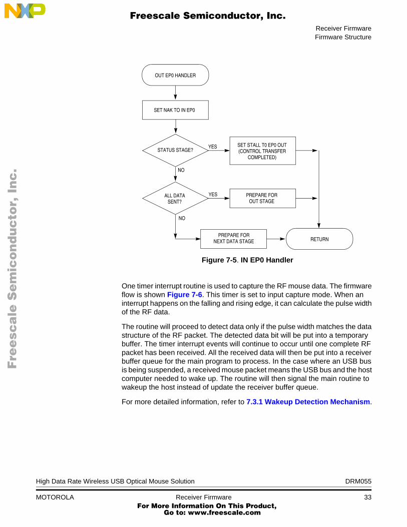
Figure 7-3, Figure 7-4, and Figure 7-5 show the routines handling control transfers. Control transfers have two or three transaction stages: setup, data (optional), and status as shown below:
• Control write: SETUP, OUT, OUT, OUT... IN
• Control read: SETUP, IN, IN, IN... OUT
• No Data control: SETUP, IN
The firmware first distinguishes the kind of control transfer and then does the corresponding preparation for the next stage.
Fre
esc
ale
Se
mic
on
du
cto
r, I
Freescale Semiconductor, Inc.
For More Information On This Product, Go to: www.freescale.com
nc
...
DRM055 High Data Rate Wireless USB Optical Mouse Solution
30 Receiver Firmware MOTOROLA
Receiver Firmware
Figure 7-1. Firmware Flow
MAIN
NEWRECEIVED MOUSEDATA IN BUFFER?
CONVERT DATATO MOUSE REPORT
DEVICECONFIGURED?
NEW ENDPOINT 1REPORT?
NEW ENDPOINT 2REPORT?
USB IDLE FOR3 ms?
EP1 TX BUFFEREMPTY?
EP2 TX BUFFEREMPTY?
RF PACKETDETECTED OR RESUME
FROM HOST?
TX EP1 IN REPORT
TX EP2 IN REPORT
SUSPEND DEVICE
YES
NO
NO
YES YES
YES YES
YES
NO
NO
NO
YES
Fre
esc
ale
Se
mic
on
du
cto
r, I
Freescale Semiconductor, Inc.
For More Information On This Product, Go to: www.freescale.com
nc
...

Receiver FirmwareFirmware Structure
High Data Rate Wireless USB Optical Mouse Solution DRM055
MOTOROLA Receiver Firmware 31
Figure 7-2. USB Interrupt Routine
USB INTERRUPT ROUTINE
EOP?
RESET SUSPEND COUNTER
OUT TOKENTO EP0?
RESUME FROMHOST?
RETURN FROM INTERRUPT
EP2 TX COMPLETED?
SETUP?
EP1 TX COMPLETED?
EP0 TX COMPLETED?
YES
NO
NO
YES
YES
YES
YES
YES
YES
SETUP HANDLER
OUT EP0 HANDLER
IN EP0 HANDLER
DISABLE EP1 TRANSMIT
DISABLE EP2 TRANSMIT
CLEAR RESUME FLAG
AND CLEAR EP1 TX FLAG
AND CLEAR EP2 TX FLAG
NO
NO
NO
NO
NO
Fre
esc
ale
Se
mic
on
du
cto
r, I
Freescale Semiconductor, Inc.
For More Information On This Product, Go to: www.freescale.com
nc
...
DRM055 High Data Rate Wireless USB Optical Mouse Solution
32 Receiver Firmware MOTOROLA
Receiver Firmware
Figure 7-3. Setup Routine
Figure 7-4. OUT EP0 Handler
SETUP HANDLER
STANDARD DEVICE YES
1. UNINSTALL EP0 IN AND OUT
HANDLE STANDARD
2. COPY 8-BYTE SETUP DATA
DEVICE REQUEST
NO
TO RAM BUFFER3. CLEAR EP0 RX FLAG4. SET NAK TO IN EP0
HID CLASS
RETURN STALL
HANDLE HIDCLASS REQUEST
RETURN
YES
NO
REQUEST?
REQUEST?
OUT EP0 HANDLER
STATUS STAGE?YES
NO
VALID DATA
RETURN STALL RETURN
YES
NO
1. SET NAK TO EP0 IN2. SET STALL TO EP0 OUT(CONTROL TRANSFER
COMPLETED)
1. COPY DATA TO BUFFER2. PROCESS OUT DATA
Fre
esc
ale
Se
mic
on
du
cto
r, I
Freescale Semiconductor, Inc.
For More Information On This Product, Go to: www.freescale.com
nc
...
Receiver FirmwareFirmware Structure
High Data Rate Wireless USB Optical Mouse Solution DRM055
MOTOROLA Receiver Firmware 33
Figure 7-5. IN EP0 Handler
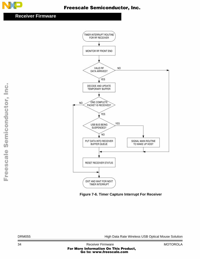
One timer interrupt routine is used to capture the RF mouse data. The firmware flow is shown Figure 7-6. This timer is set to input capture mode. When an interrupt happens on the falling and rising edge, it can calculate the pulse width of the RF data.
The routine will proceed to detect data only if the pulse width matches the data structure of the RF packet. The detected data bit will be put into a temporary buffer. The timer interrupt events will continue to occur until one complete RF packet has been received. All the received data will then be put into a receiver buffer queue for the main program to process. In the case where an USB bus is being suspended, a received mouse packet means the USB bus and the host computer needed to wake up. The routine will then signal the main routine to wakeup the host instead of update the receiver buffer queue.
For more detailed information, refer to 7.3.1 Wakeup Detection Mechanism.
OUT EP0 HANDLER
STATUS STAGE?YES
NO
RETURN
YES
NO
SET NAK TO IN EP0
SET STALL T0 EP0 OUT(CONTROL TRANSFER
COMPLETED)
PREPARE FOROUT STAGE
ALL DATASENT?
PREPARE FORNEXT DATA STAGE
Fre
esc
ale
Se
mic
on
du
cto
r, I
Freescale Semiconductor, Inc.
For More Information On This Product, Go to: www.freescale.com
nc
...
DRM055 High Data Rate Wireless USB Optical Mouse Solution
34 Receiver Firmware MOTOROLA
Receiver Firmware
Figure 7-6. Timer Capture Interrupt For Receiver
TIMER INTERRUPT ROUTINE
MONITOR RF FRONT END
USB BUS BEINGSUSPENDED?
VALID RF
ONE COMPLETE
NO
YES
YES
YES
DECODE AND UPDATETEMPORARY BUFFER
FOR RF RECEIVER
DATA ARRIVED?
PACKET IS RECEIVED?NO
NO
RESET RECEIVER STATUS
PUT DATA INTO RECEIVERBUFFER QUEUE
EXIT AND WAIT FOR NEXTTIMER INTERRUPT
SIGNAL MAIN ROUTINETO WAKE UP HOST
Fre
esc
ale
Se
mic
on
du
cto
r, I
Freescale Semiconductor, Inc.
For More Information On This Product, Go to: www.freescale.com
nc
...
Receiver FirmwareUSB Report
High Data Rate Wireless USB Optical Mouse Solution DRM055
MOTOROLA Receiver Firmware 35
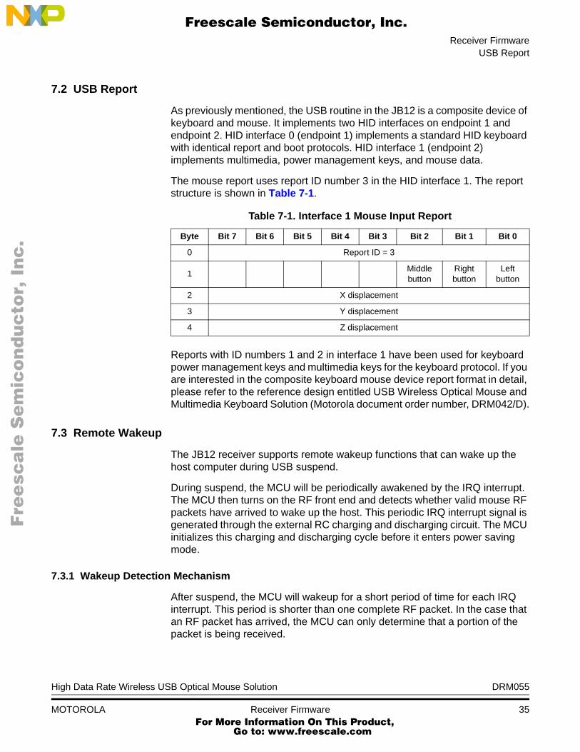
7.2 USB Report
As previously mentioned, the USB routine in the JB12 is a composite device of keyboard and mouse. It implements two HID interfaces on endpoint 1 and endpoint 2. HID interface 0 (endpoint 1) implements a standard HID keyboard with identical report and boot protocols. HID interface 1 (endpoint 2) implements multimedia, power management keys, and mouse data.
The mouse report uses report ID number 3 in the HID interface 1. The report structure is shown in Table 7-1.
Reports with ID numbers 1 and 2 in interface 1 have been used for keyboard power management keys and multimedia keys for the keyboard protocol. If you are interested in the composite keyboard mouse device report format in detail, please refer to the reference design entitled USB Wireless Optical Mouse and Multimedia Keyboard Solution (Motorola document order number, DRM042/D).
7.3 Remote Wakeup
The JB12 receiver supports remote wakeup functions that can wake up the host computer during USB suspend.
During suspend, the MCU will be periodically awakened by the IRQ interrupt. The MCU then turns on the RF front end and detects whether valid mouse RF packets have arrived to wake up the host. This periodic IRQ interrupt signal is generated through the external RC charging and discharging circuit. The MCU initializes this charging and discharging cycle before it enters power saving mode.
7.3.1 Wakeup Detection Mechanism
After suspend, the MCU will wakeup for a short period of time for each IRQ interrupt. This period is shorter than one complete RF packet. In the case that an RF packet has arrived, the MCU can only determine that a portion of the packet is being received.
Table 7-1. Interface 1 Mouse Input Report
Byte Bit 7 Bit 6 Bit 5 Bit 4 Bit 3 Bit 2 Bit 1 Bit 0
0 Report ID = 3
1Middlebutton
Right button
Leftbutton
2 X displacement
3 Y displacement
4 Z displacement
Fre
esc
ale
Se
mic
on
du
cto
r, I
Freescale Semiconductor, Inc.
For More Information On This Product, Go to: www.freescale.com
nc
...

DRM055 High Data Rate Wireless USB Optical Mouse Solution
36 Receiver Firmware MOTOROLA
Receiver Firmware
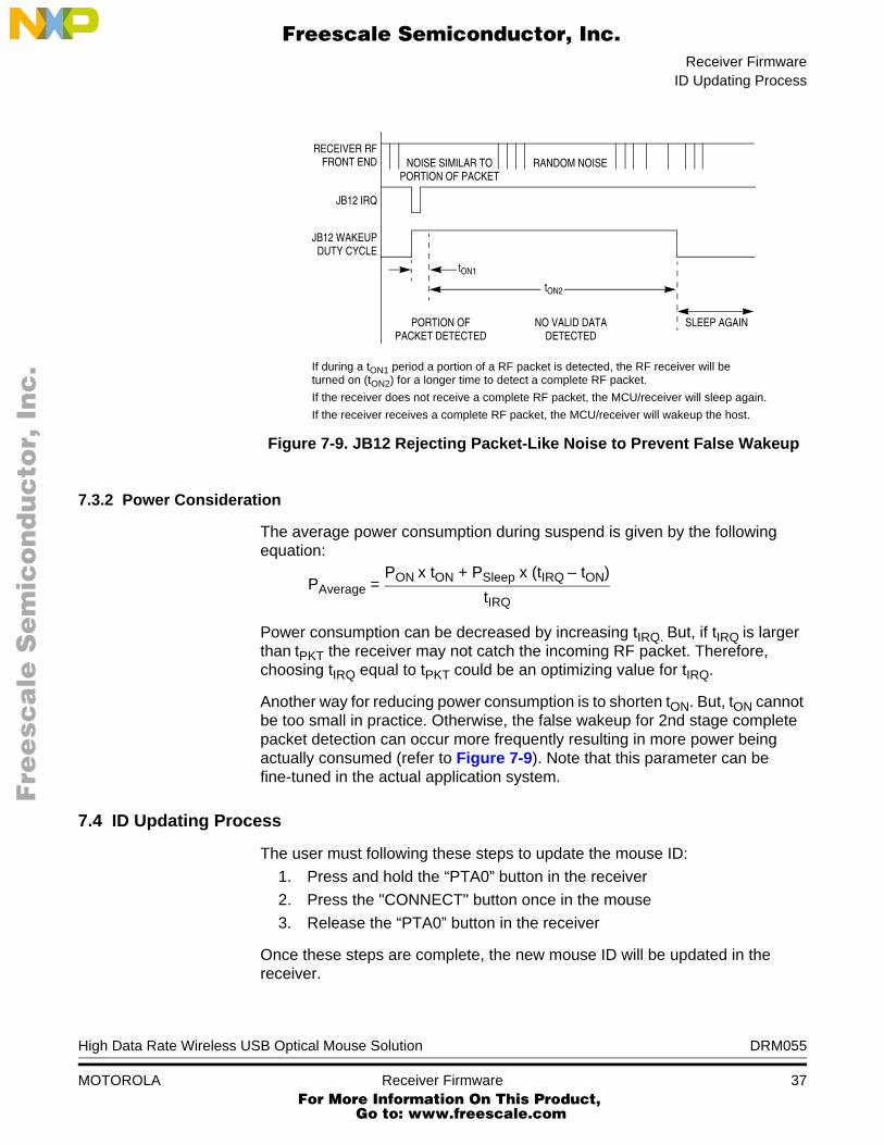
For this short detection period, there is the possibility that the noise hit into the RF front end would have a pattern like a packet portion. Therefore, if a packet portion is detected, the MCU will turn on for a longer duty cycle. This duty cycle is for receiving the next complete RF packet that can wake up the host.
The mechanism and the timing parameters for detecting a wakeup packet are shown in Figure 7-7, Figure 7-8, and Figure 7-9.
Figure 7-7. Timing Parameters for Packet Detection
Figure 7-8. Detection of Valid Wakeup Packets
RF PACKET
tPKT
tIRQ
tON1
tSleep
TRANSMITTERMOUSE PACKET
JB12 IRQ
JB12 WAKEUPDUTY CYCLE
tPKT: Length of one complete RF packettIRQ: Time interval of successive IRQ wakeup periods during device suspend.tON1: Duration of MCU being turned on in each IRQ wakeup period. MCU is turned
on in this period to detect a (portion of) RF packet has been received.
TRANSMITTERMOUSE PACKET
JB12 IRQ
JB12 WAKEUPDUTY CYCLE
RF PACKET NEXT MOUSE PACKET
tON1tON2
VALID DATA DETECTED
JB12 WILL WAKE UP
RF PACKET
PORTION OFPACKET DETECTED
THE HOST
If during a tON1 period a portion of a RF packet is detected, the RF receiver will turn on (tON2) for a longer time to detect a complete RF packet.
If one complete RF packet is received, the MCU will wake up the host.
Fre
esc
ale
Se
mic
on
du
cto
r, I
Freescale Semiconductor, Inc.
For More Information On This Product, Go to: www.freescale.com
nc
...
Receiver FirmwareID Updating Process
High Data Rate Wireless USB Optical Mouse Solution DRM055
MOTOROLA Receiver Firmware 37
Figure 7-9. JB12 Rejecting Packet-Like Noise to Prevent False Wakeup
7.3.2 Power Consideration
The average power consumption during suspend is given by the following equation:
Power consumption can be decreased by increasing tIRQ. But, if tIRQ is larger than tPKT the receiver may not catch the incoming RF packet. Therefore, choosing tIRQ equal to tPKT could be an optimizing value for tIRQ.
Another way for reducing power consumption is to shorten tON. But, tON cannot be too small in practice. Otherwise, the false wakeup for 2nd stage complete packet detection can occur more frequently resulting in more power being actually consumed (refer to Figure 7-9). Note that this parameter can be fine-tuned in the actual application system.
7.4 ID Updating Process
The user must following these steps to update the mouse ID:
1. Press and hold the “PTA0” button in the receiver
2. Press the "CONNECT" button once in the mouse
3. Release the “PTA0” button in the receiver
Once these steps are complete, the new mouse ID will be updated in the receiver.
RECEIVER RFFRONT END
JB12 IRQ
JB12 WAKEUPDUTY CYCLE
PORTION OFPACKET DETECTED
NO VALID DATADETECTED
SLEEP AGAIN
NOISE SIMILAR TOPORTION OF PACKET
RANDOM NOISE
tON1
tON2
If during a tON1 period a portion of a RF packet is detected, the RF receiver will beturned on (tON2) for a longer time to detect a complete RF packet.
If the receiver does not receive a complete RF packet, the MCU/receiver will sleep again.
If the receiver receives a complete RF packet, the MCU/receiver will wakeup the host.
PAverage = PON x tON + PSleep x (tIRQ – tON)
tIRQ
Fre
esc
ale
Se
mic
on
du
cto
r, I
Freescale Semiconductor, Inc.
For More Information On This Product, Go to: www.freescale.com
nc
...

DRM055 High Data Rate Wireless USB Optical Mouse Solution
38 Receiver Firmware MOTOROLA
Receiver Firmware
Fre
esc
ale
Se
mic
on
du
cto
r, I
Freescale Semiconductor, Inc.
For More Information On This Product, Go to: www.freescale.com
nc
...
High Data Rate Wireless USB Optical Mouse Solution DRM055
MOTOROLA Testing and Customization 39
Designer Reference Manual — DRM055
Section 8. Testing and Customization
8.1 Testing
This solution was tested under different Windows Operating Systems on several different PCs for USB compatibility. These tests included:
• USB compliance test using Command Verifier, Version 1.2
• Compatibility tests under Windows 98SE, 2000, and XP
• Compatibility tests under AMD 750, Intel 810 and 845 chip set desktops, and IBM Thinkpad T23, DELL Latitude C640
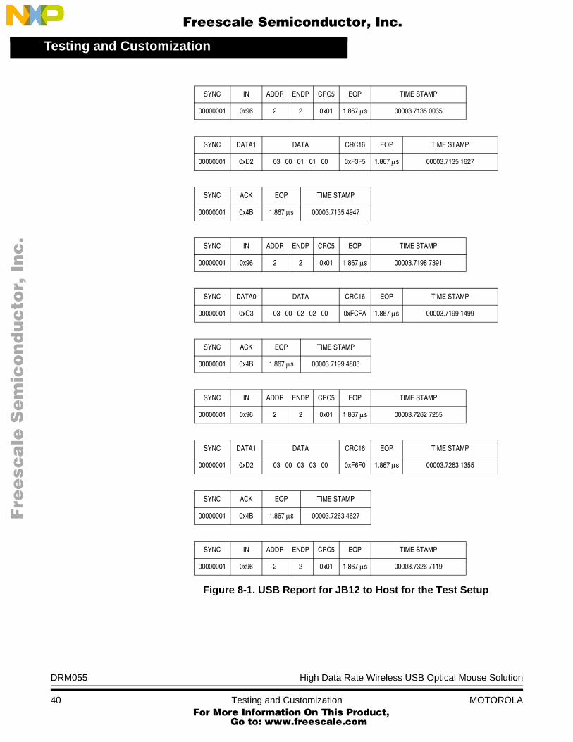
The integrity of the RF data link between the mouse and receiver had been verified by recording the actual USB report from the receiver to host.
A test had been setup where the mouse transmitter was sending some pre-defined RF data continuously. At the receiver side, an USB analyzer had been connected between the JB12 and the host computer. The analyzer captured the USB data from the JB12 to host PC. The captured data was then compared with pre-defined data from the mouse.
These tests showed that the JB12 solution can achieve an average valid USB data report rate of about 10 ms without loss of any data from the transmitter side. Refer to Figure 8-1.
8.2 Hardware Customization
8.2.1 Optical Mouse Transmitter
The step-up DC-to-DC converter (NCP1400ASN33T1) is for reference only, customers can choose any regulator they prefer. The LEDs for the sensor and ZLED can be connected to the regulator output or connected to the batteries output. The advantage of connecting to the regulator output is that the system can work in a lower voltage, but the drawback is higher current consumption. The advantage of connecting to the batteries output is the lower power consumption but the system will not work properly if battery voltage is below 2.5 V.
Fre
esc
ale
Se
mic
on
du
cto
r, I
Freescale Semiconductor, Inc.
For More Information On This Product, Go to: www.freescale.com
nc
...
DRM055 High Data Rate Wireless USB Optical Mouse Solution
40 Testing and Customization MOTOROLA
Testing and Customization
SYNC IN ADDR ENDP CRC5 EOP TIME STAMP
00000001 0x96 2 2 0x01 1.867 µs 00003.7135 0035
SYNC DATA1 DATA CRC16 EOP TIME STAMP
00000001 0xD2 03 00 01 01 00 0xF3F5 1.867 µs 00003.7135 1627
SYNC ACK EOP TIME STAMP
00000001 0x4B 1.867 µs 00003.7135 4947
SYNC IN ADDR ENDP CRC5 EOP TIME STAMP
00000001 0x96 2 2 0x01 1.867 µs 00003.7198 7391
SYNC DATA0 DATA CRC16 EOP TIME STAMP
00000001 0xC3 03 00 02 02 00 0xFCFA 1.867 µs 00003.7199 1499
SYNC ACK EOP TIME STAMP
00000001 0x4B 1.867 µs 00003.7199 4803
SYNC IN ADDR ENDP CRC5 EOP TIME STAMP
00000001 0x96 2 2 0x01 1.867 µs 00003.7262 7255
SYNC DATA1 DATA CRC16 EOP TIME STAMP
00000001 0xD2 03 00 03 03 00 0xF6F0 1.867 µs 00003.7263 1355
SYNC ACK EOP TIME STAMP
00000001 0x4B 1.867 µs 00003.7263 4627
SYNC IN ADDR ENDP CRC5 EOP TIME STAMP
00000001 0x96 2 2 0x01 1.867 µs 00003.7326 7119
Figure 8-1. USB Report for JB12 to Host for the Test Setup
Fre
esc
ale
Se
mic
on
du
cto
r, I
Freescale Semiconductor, Inc.
For More Information On This Product, Go to: www.freescale.com
nc
...
Testing and CustomizationHardware Customization
High Data Rate Wireless USB Optical Mouse Solution DRM055
MOTOROLA Testing and Customization 41
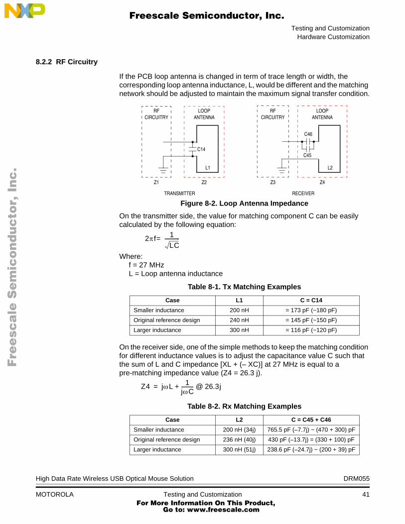
8.2.2 RF Circuitry
If the PCB loop antenna is changed in term of trace length or width, the corresponding loop antenna inductance, L, would be different and the matching network should be adjusted to maintain the maximum signal transfer condition.
Figure 8-2. Loop Antenna Impedance
On the transmitter side, the value for matching component C can be easily calculated by the following equation:
Where:f = 27 MHzL = Loop antenna inductance
On the receiver side, one of the simple methods to keep the matching condition for different inductance values is to adjust the capacitance value C such that the sum of L and C impedance [XL + (– XC)] at 27 MHz is equal to a pre-matching impedance value (Z4 = 26.3 j).
Table 8-1. Tx Matching Examples
Case L1 C = C14
Smaller inductance 200 nH = 173 pF (~180 pF)
Original reference design 240 nH = 145 pF (~150 pF)
Larger inductance 300 nH = 116 pF (~120 pF)
Table 8-2. Rx Matching Examples
Case L2 C = C45 + C46
Smaller inductance 200 nH (34j) 765.5 pF (–7.7j) ~ (470 + 300) pF
Original reference design 236 nH (40j) 430 pF (–13.7j) = (330 + 100) pF
Larger inductance 300 nH (51j) 238.6 pF (–24.7j) ~ (200 + 39) pF
LOOPANTENNA
RFCIRCUITRY
C14
Z1 Z2
TRANSMITTER
LOOPANTENNA
RFCIRCUITRY
Z3 Z4
RECEIVER
C45
C46
L1 L2
2πf 1
LC------------=
Z4 jωL 1jωC---------- 26.3j@+=
Fre
esc
ale
Se
mic
on
du
cto
r, I
Freescale Semiconductor, Inc.
For More Information On This Product, Go to: www.freescale.com
nc
...
DRM055 High Data Rate Wireless USB Optical Mouse Solution
42 Testing and Customization MOTOROLA
Testing and Customization
8.3 Firmware Customization
8.3.1 Mouse Transmitter
To customize the mouse transmitter:
• Set compiler option to store the ID code in RAM or in FLASH
• Set the timing parameters for power management
8.3.2 Receiver
To customize the receiver:
• Change vendor ID, product ID, and product revision number in the device descriptor table in "KBD-MSE.H"
• Change the report descriptor in "KBD-MSE.H" if necessary
Fre
esc
ale
Se
mic
on
du
cto
r, I
Freescale Semiconductor, Inc.
For More Information On This Product, Go to: www.freescale.com
nc
...

Fre
esc
ale
Se
mic
on
du
cto
r, I
Freescale Semiconductor, Inc.
For More Information On This Product, Go to: www.freescale.com
nc
...

HOW TO REACH US:
USA/EUROPE/LOCATIONS NOT LISTED:Motorola Literature DistributionP.O. Box 5405Denver, Colorado 802171-800-521-6274 or 480-768-2130
JAPAN:Motorola Japan Ltd.SPS, Technical Information Center3-20-1, Minami-Azabu, Minato-kuTokyo 106-8573, Japan81-3-3440-3569
ASIA/PACIFIC:Motorola Semiconductors H.K. Ltd.Silicon Harbour Centre2 Dai King StreetTai Po Industrial EstateTai Po, N.T., Hong Kong852-26668334
HOME PAGE:http://motorola.com/semiconductors
DRM055/DRev. 01/2004
Information in this document is provided solely to enable system and software implementers to use Motorola products. There are no express or implied copyright licenses granted hereunder to design or fabricate any integrated circuits or integrated circuits based on the information in this document.
Motorola reserves the right to make changes without further notice to any products herein. Motorola makes no warranty, representation or guarantee regarding the suitability of its products for any particular purpose, nor does Motorola assume any liability arising out of the application or use of any product or circuit, and specifically disclaims any and all liability, including without limitation consequential or incidental damages. “Typical” parameters that may be provided in Motorola data sheets and/or specifications can and do vary in different applications and actual performance may vary over time. All operating parameters, including “Typicals”, must be validated for each customer application by customer’s technical experts. Motorola does not convey any license under its patent rights nor the rights of others. Motorola products are not designed, intended, or authorized for use as components in systems intended for surgical implant into the body, or other applications intended to support or sustain life, or for any other application in which the failure of the Motorola product could create a situation where personal injury or death may occur. Should Buyer purchase or use Motorola products for any such unintended or unauthorized application, Buyer shall indemnify and hold Motorola and its officers, employees, subsidiaries, affiliates, and distributors harmless against all claims, costs, damages, and expenses, and reasonable attorney fees arising out of, directly or indirectly, any claim of personal injury or death associated with such unintended or unauthorized use, even if such claim alleges that Motorola was negligent regarding the design or manufacture of the part.
MOTOROLA and the Stylized M Logo are registered in the US Patent and Trademark Office. All other product or service names are the property of their respective owners. Motorola, Inc. is an Equal Opportunity/Affirmative Action Employer.
© Motorola Inc. 2004
Fre
esc
ale
Se
mic
on
du
cto
r, I
Freescale Semiconductor, Inc.
For More Information On This Product, Go to: www.freescale.com
nc
...