Embed Size (px)
Citation preview

Pin Configurations
General DescriptionThe DS18S20 digital thermometer provides 9-bit Celsius temperature measurements and has an alarm function with nonvolatile user-programmable upper and lower trig-ger points. The DS18S20 communicates over a 1-Wire bus that by definition requires only one data line (and ground) for communication with a central microprocessor. In addition, the DS18S20 can derive power directly from the data line (“parasite power”), eliminating the need for an external power supply.Each DS18S20 has a unique 64-bit serial code, which allows multiple DS18S20s to function on the same 1-Wire bus. Thus, it is simple to use one microprocessor to control many DS18S20s distributed over a large area. Applications that can benefit from this feature include HVAC environmental controls, temperature monitoring systems inside buildings, equipment, or machinery, and process monitoring and control systems.
Applications Thermostatic Controls Industrial Systems Consumer Products Thermometers Thermally Sensitive Systems
Benefits and Features Unique 1-Wire® Interface Requires Only One Port
Pin for Communication Maximize System Accuracy in Broad Range of
Thermal Management Applications• Measures Temperatures from -55°C to +125°C
(-67°F to +257°F)• ±0.5°C Accuracy from -10°C to +85°C• 9-Bit Resolution• No External Components Required
Parasite Power Mode Requires Only 2 Pins for Operation (DQ and GND)
Simplifies Distributed Temperature-Sensing Applications with Multidrop Capability• Each Device Has a Unique 64-Bit Serial Code
Stored in On-Board ROM Flexible User-Definable Nonvolatile (NV) Alarm Settings
with Alarm Search Command Identifies Devices with Temperatures Outside Programmed Limits
Available in 8-Pin SO (150 mils) and 3-Pin TO-92 Packages
Ordering Information appears at end of data sheet.
1-Wire is a registered trademark of Maxim Integrated Products, Inc.
19-5474; Rev 3; 4/15
BOTTOM VIEW
2
N.C.
N.C.
VDD
DQ
N.C.
N.C.
N.C.
GND
DS18S20
SO (150 mils)(DS18S20Z)
+1
4
3
7
8
5
6
DS18S20
1 2 3
GND DQ VDD
1
1 2 3
TOP VIEW
TO-92 (DS18S20)
DS18S20 High-Precision 1-Wire Digital Thermometer

Voltage Range on Any Pin Relative to Ground ....-0.5V to +6.0VContinuous Power Dissipation (TA = +70°C)
8-Pin SO (derate 5.9mW/°C above +70°C) ..............470.6mW 3-Pin TO-92 (derate 6.3mW/°C above +70°C) ............500mW
Operating Temperature Range ......................... -55°C to +125°C
Storage Temperature Range ............................ -55°C to +125°CLead Temperature (soldering, 10s) .................................+260°CSoldering Temperature (reflow)
Lead(Pb)-free.............................................................. .+260°C Containing lead(Pb) .....................................................+240°C
Note 1: All voltages are referenced to ground. Note 2: The Pullup Supply Voltage specification assumes that the pullup device is ideal, and therefore the high level of the pul-
lup is equal to VPU. In order to meet the VIH spec of the DS18S20, the actual supply rail for the strong pullup transistor must include margin for the voltage drop across the transistor when it is turned on; thus: VPU_ACTUAL = VPU_IDEAL + VTRANSISTOR.
Note 3: See typical performance curve in Figure 1.Note 4: Logic-low voltages are specified at a sink current of 4mA.Note 5: To guarantee a presence pulse under low voltage parasite power conditions, VILMAX may have to be reduced to as
low as 0.5V. Note 6: Logic-high voltages are specified at a source current of 1mA.Note 7: Standby current specified up to +70°C. Standby current typically is 3µA at +125°C.Note 8: To minimize IDDS, DQ should be within the following ranges: GND ≤ DQ ≤ GND + 0.3V or VDD – 0.3V ≤ DQ ≤ VDD.Note 9: Active current refers to supply current during active temperature conversions or EEPROM writes.Note 10: DQ line is high (“high-Z” state).Note 11: Drift data is based on a 1000-hour stress test at +125°C with VDD = 5.5V.
(VDD = 3.0V to 5.5V, TA = -55°C to +125°C, unless otherwise noted.)
PARAMETER SYMBOL CONDITIONS MIN TYP MAX UNITSSupply Voltage VDD Local Power (Note 1) +3.0 +5.5 V
Pullup Supply Voltage VPUParasite Power
(Note 1, 2)+3.0 +5.5
VLocal Power +3.0 VDD
Thermometer Error tERR-10°C to +85°C
(Note 3)±0.5
°C-55°C to +125°C ±2
Input Logic-Low VIL (Note 1, 4, 5) -0.3 +0.8 V
Input Logic-High VIHLocal Power
(Note 1, 6)+2.2 The lower of
5.5 or VDD + 0.3
VParasite Power +3.0
Sink Current IL VI/O = 0.4V (Note 1) 4.0 mA
Standby Current IDDS (Note 7, 8) 750 1000 nA
Active Current IDD VDD = 5V (Note 9) 1 1.5 mA
DQ Input Current IDQ (Note 10) 5 µA
Drift (Note 11) ±0.2 °C
DS18S20 High-Precision 1-Wire Digital Thermometer
www.maximintegrated.com Maxim Integrated 2
Absolute Maximum Ratings
These are stress ratings only and functional operation of the device at these or any other conditions above those indicated in the operation sections of this specification is not implied. Exposure to absolute maximum rating conditions for extended periods of time may affect reliability.
DC Electrical Characteristics

(VDD = 3.0V to 5.5V, TA = -55°C to +100°C, unless otherwise noted.)
(VDD = 3.0V to 5.5V; TA = -55°C to +125°C, unless otherwise noted.)
Note 12: See the timing diagrams in Figure 2.Note 13: Under parasite power, if tRSTL > 960µs, a power-on reset may occur.
PARAMETER SYMBOL CONDITIONS MIN TYP MAX UNITSNV Write Cycle Time tWR 2 10 ms
EEPROM Writes NEEWR -55°C to +55°C 50k writes
EEPROM Data Retention tEEDR -55°C to +55°C 10 years
PARAMETER SYMBOL CONDITIONS MIN TYP MAX UNITSTemperature Conversion Time tCONV (Note 12) 750 ms
Time to Strong Pullup On tSPON Start Convert T Command Issued 10 µs
Time Slot tSLOT (Note 12) 60 120 µs
Recovery Time tREC (Note 12) 1 µs
Write 0 Low Time tLOW0 (Note 12) 60 120 µs
Write 1 Low Time tLOW1 (Note 12) 1 15 µs
Read Data Valid tRDV (Note 12) 15 µs
Reset Time High tRSTH (Note 12) 480 µs
Reset Time Low tRSTL (Note 12, 13) 480 µs
Presence-Detect High tPDHIGH (Note 12) 15 60 µs
Presence-Detect Low tPDLOW (Note 12) 60 240 µs
Capacitance CIN/OUT 25 pF
Figure 1. Typical Performance Curve
DS18S20 TYPICAL ERROR CURVE0.50.40.30.20.1
0-0.1-0.2-0.3-0.4
-0.5
THER
MOME
TER
ERRO
R (°C
)
0 7010 20 30 40 50 60
TEMPERATURE (°C)
+3s ERROR
MEAN ERROR
-3s ERROR
DS18S20 High-Precision 1-Wire Digital Thermometer
www.maximintegrated.com Maxim Integrated 3
AC Electrical Characteristics—NV Memory
AC Electrical Characteristics

PINNAME FUNCTION
TO-92 SO1 5 GND Ground
2 4 DQ Data Input/Output. Open-drain 1-Wire interface pin. Also provides power to the device when used in parasite power mode (see the Powering the DS18S20 section.)
3 3 VDD Optional VDD. VDD must be grounded for operation in parasite power mode.
— 1, 2, 6, 7, 8 N.C. No Connection
Figure 2. Timing Diagrams
START OF NEXT CYCLE
1-Wire WRITE ZERO TIME SLOT
tREC
tSLOT
tLOW0
1-Wire READ ZERO TIME SLOT
tREC
tSLOTSTART OF NEXT CYCLE
tRDV
1-Wire RESET PULSE
1-Wire PRESENCE DETECT
tRSTL tRSTH
tPDHIGH
PRESENCE DETECT
tPDLOW
RESET PULSE FROM HOST
DS18S20 High-Precision 1-Wire Digital Thermometer
www.maximintegrated.com Maxim Integrated 4
Pin Description

OverviewFigure 3 shows a block diagram of the DS18S20, and pin descriptions are given in the Pin Description table. The 64-bit ROM stores the device’s unique serial code. The scratchpad memory contains the 2-byte temperature register that stores the digital output from the temperature sensor. In addition, the scratchpad provides access to the 1-byte upper and lower alarm trigger registers (TH and TL). The TH and TL registers are nonvolatile (EEPROM), so they will retain data when the device is powered down.The DS18S20 uses Maxim’s exclusive 1-Wire bus proto-col that implements bus communication using one control signal. The control line requires a weak pullup resistor since all devices are linked to the bus via a 3-state or open-drain port (the DQ pin in the case of the DS18S20). In this bus system, the microprocessor (the master device) identifies and addresses devices on the bus using each device’s unique 64-bit code. Because each device has a unique code, the number of devices that can be addressed on one bus is virtually unlimited. The 1-Wire bus protocol, including detailed explanations of the commands and “time slots,” is covered in the 1-Wire Bus System section.Another feature of the DS18S20 is the ability to operate without an external power supply. Power is instead sup-plied through the 1-Wire pullup resistor via the DQ pin when the bus is high. The high bus signal also charges an
internal capacitor (CPP), which then supplies power to the device when the bus is low. This method of deriving power from the 1-Wire bus is referred to as “parasite power.” As an alternative, the DS18S20 may also be powered by an external supply on VDD.
Operation—Measuring TemperatureThe core functionality of the DS18S20 is its direct-to-dig-ital temperature sensor. The temperature sensor output has 9-bit resolution, which corresponds to 0.5°C steps. The DS18S20 powers-up in a low-power idle state; to initiate a temperature measurement and A-to-D conver-sion, the master must issue a Convert T [44h] command. Following the conversion, the resulting thermal data is stored in the 2-byte temperature register in the scratch-pad memory and the DS18S20 returns to its idle state. If the DS18S20 is powered by an external supply, the master can issue “read-time slots” (see the 1-Wire Bus System section) after the Convert T command and the DS18S20 will respond by transmitting 0 while the tem-perature conversion is in progress and 1 when the con-version is done. If the DS18S20 is powered with parasite power, this notification technique cannot be used since the bus must be pulled high by a strong pullup during the entire temperature conversion. The bus requirements for parasite power are explained in detail in the Powering The DS18S20 section.
Figure 3. DS18S20 Block Diagram
VPU
64-BIT ROMAND
1-Wire PORT
DQ
VDD
INTERNAL VDD
CPP
PARASITE POWER CIRCUIT MEMORYCONTROL LOGIC
SCRATCHPAD
8-BIT CRCGENERATOR
TEMPERATURESENSOR
ALARM HIGH TRIGGER (TH)REGISTER (EEPROM)
ALARM LOW TRIGGER (TL)REGISTER (EEPROM)
GND
DS18S204.7kΩ
POWER-SUPPLY SENSE
DS18S20 High-Precision 1-Wire Digital Thermometer
www.maximintegrated.com Maxim Integrated 5

The DS18S20 output data is calibrated in degrees cen-tigrade; for Fahrenheit applications, a lookup table or conversion routine must be used. The temperature data is stored as a 16-bit sign-extended two’s complement num-ber in the temperature register (see Figure 4). The sign bits (S) indicate if the temperature is positive or negative: for positive numbers S = 0 and for negative numbers S = 1. Table 1 gives examples of digital output data and the corresponding temperature reading.Resolutions greater than 9 bits can be calculated using the data from the temperature, COUNT REMAIN and COUNT PER °C registers in the scratchpad. Note that the COUNT PER °C register is hard-wired to 16 (10h). After reading the scratchpad, the TEMP_READ value is obtained by truncating the 0.5°C bit (bit 0) from the temperature data (see Figure 4). The extended resolution temperature can then be calculated using the following equation:
TEMPERATURE TEMP_READ 0.25COUNT_PER_C COUNT_REMAIN
COUNT_PER_C
= −−
+
Operation—Alarm SignalingAfter the DS18S20 performs a temperature conversion, the temperature value is compared to the user-defined two’s complement alarm trigger values stored in the 1-byte TH and TL registers (see Figure 5). The sign bit (S) indicates if the value is positive or negative: for positive numbers S = 0 and for negative numbers S = 1. The TH and TL registers are nonvolatile (EEPROM) so they will retain data when the device is powered down. TH and TL can be accessed through bytes 2 and 3 of the scratchpad as explained in the Memory section.Only bits 8 through 1 of the temperature register are used in the TH and TL comparison since TH and TL are 8-bit registers. If the measured temperature is lower than or equal to TL or higher than TH, an alarm condition exists and an alarm flag is set inside the DS18S20. This flag is updated after every temperature measurement; therefore, if the alarm condition goes away, the flag will be turned off after the next temperature conversion.
Table 1. Temperature/Data Relationship
*The power-on reset value of the temperature register is +85°C.
TEMPERATURE (°C) DIGITAL OUTPUT (BINARY) DIGITAL OUTPUT (HEX)+85.0* 0000 0000 1010 1010 00AAh
+25.0 0000 0000 0011 0010 0032h
+0.5 0000 0000 0000 0001 0001h
0 0000 0000 0000 0000 0000h
-0.5 1111 1111 1111 1111 FFFFh
-25.0 1111 1111 1100 1110 FFCEh
-55.0 1111 1111 1001 0010 FF92h
Figure 4. Temperature Register Format
Figure 5. TH and TL Register Format
BIT 7 BIT 6 BIT 5 BIT 4 BIT 3 BIT 2 BIT 1 BIT 0LS BYTE 26 25 24 23 22 21 20 2-1
BIT 15 BIT 14 BIT 13 BIT 12 BIT 11 BIT 10 BIT 9 BIT 8
MS BYTE S S S S S S S S
S = SIGN
BIT 7 BIT 6 BIT 5 BIT 4 BIT 3 BIT 2 BIT 1 BIT 0S 26 25 25 25 22 21 20
DS18S20 High-Precision 1-Wire Digital Thermometer
www.maximintegrated.com Maxim Integrated 6

The master device can check the alarm flag status of all DS18S20s on the bus by issuing an Alarm Search [ECh] command. Any DS18S20s with a set alarm flag will respond to the command, so the master can determine exactly which DS18S20s have experienced an alarm condition. If an alarm condition exists and the TH or TL settings have changed, another temperature conversion should be done to validate the alarm condition.
Powering The DS18S20The DS18S20 can be powered by an external supply on the VDD pin, or it can operate in “parasite power” mode, which allows the DS18S20 to function without a local external supply. Parasite power is very useful for applica-tions that require remote temperature sensing or those with space constraints. Figure 3 shows the DS18S20’s parasite-power control circuitry, which “steals” power from the 1-Wire bus via the DQ pin when the bus is high. The stolen charge powers the DS18S20 while the bus is high, and some of the charge is stored on the parasite power capacitor (CPP) to provide power when the bus is low. When the DS18S20 is used in parasite power mode, the VDD pin must be connected to ground.In parasite power mode, the 1-Wire bus and CPP can provide sufficient current to the DS18S20 for most opera-tions as long as the specified timing and voltage require-ments are met (see the DC Electrical Characteristics and the AC Electrical Characteristics). However, when the DS18S20 is performing temperature conversions or copying data from the scratchpad memory to EEPROM, the operating current can be as high as 1.5mA. This current can cause an unacceptable voltage drop across the weak 1-Wire pullup resistor and is more current than can be supplied by CPP. To assure that the DS18S20 has sufficient supply current, it is necessary to provide a strong pullup on the 1-Wire bus whenever temperature
conversions are taking place or data is being copied from the scratchpad to EEPROM. This can be accomplished by using a MOSFET to pull the bus directly to the rail as shown in Figure 6. The 1-Wire bus must be switched to the strong pullup within 10µs (max) after a Convert T [44h] or Copy Scratchpad [48h] command is issued, and the bus must be held high by the pullup for the duration of the conversion (tCONV) or data transfer (tWR = 10ms). No other activity can take place on the 1-Wire bus while the pullup is enabled.The DS18S20 can also be powered by the conventional method of connecting an external power supply to the VDD pin, as shown in Figure 7. The advantage of this method is that the MOSFET pullup is not required, and the 1-Wire bus is free to carry other traffic during the tem-perature conversion time.The use of parasite power is not recommended for tem-peratures above 100°C since the DS18S20 may not be able to sustain communications due to the higher leak-age currents that can exist at these temperatures. For applications in which such temperatures are likely, it is strongly recommended that the DS18S20 be powered by an external power supply.In some situations the bus master may not know whether the DS18S20s on the bus are parasite powered or pow-ered by external supplies. The master needs this informa-tion to determine if the strong bus pullup should be used during temperature conversions. To get this information, the master can issue a Skip ROM [CCh] command fol-lowed by a Read Power Supply [B4h] command followed by a “read-time slot”. During the read-time slot, parasite powered DS18S20s will pull the bus low, and externally powered DS18S20s will let the bus remain high. If the bus is pulled low, the master knows that it must supply the strong pullup on the 1-Wire bus during temperature conversions.
Figure 6. Supplying the Parasite-Powered DS18S20 During Temperature Conversions
Figure 7. Powering the DS18S20 with an External Supply
VPU
4.7kΩ
VPU
1-Wire BUS
DS18S20
GND DQ VDD
TO OTHER 1-Wire DEVICES
µP
VDD(EXTERNAL SUPPLY)
VPU
4.7kΩ
1-Wire BUS
DS18S20
GND DQ VDD
TO OTHER 1-Wire DEVICES
µP
DS18S20 High-Precision 1-Wire Digital Thermometer
www.maximintegrated.com Maxim Integrated 7

64-Bit Lasered ROM CodeEach DS18S20 contains a unique 64-bit code (see Figure 8) stored in ROM. The least significant 8 bits of the ROM code contain the DS18S20’s 1-Wire family code: 10h. The next 48 bits contain a unique serial number. The most significant 8 bits contain a cyclic redundancy check (CRC) byte that is calculated from the first 56 bits of the ROM code. A detailed explanation of the CRC bits is provided in the CRC Generation section. The 64-bit ROM code and associated ROM function control logic allow the DS18S20 to operate as a 1-Wire device using the protocol detailed in the 1-Wire Bus System section.
MemoryThe DS18S20’s memory is organized as shown in Figure 9. The memory consists of an SRAM scratch-pad with nonvolatile EEPROM storage for the high and low alarm trigger registers (TH and TL). Note that if the DS18S20 alarm function is not used, the TH and TL reg-isters can serve as general-purpose memory. All mem-ory commands are described in detail in the DS18S20 Function Commands section.
Byte 0 and byte 1 of the scratchpad contain the LSB and the MSB of the temperature register, respectively. These bytes are read-only. Bytes 2 and 3 provide access to TH and TL registers. Bytes 4 and 5 are reserved for internal use by the device and cannot be overwritten; these bytes will return all 1s when read. Bytes 6 and 7 contain the COUNT REMAIN and COUNT PER ºC registers, which can be used to calculate extended resolution results as explained in the Operation—Measuring Temperature section.Byte 8 of the scratchpad is read-only and contains the CRC code for bytes 0 through 7 of the scratchpad. The DS18S20 generates this CRC using the method described in the CRC Generation section. Data is written to bytes 2 and 3 of the scratchpad using the Write Scratchpad [4Eh] command; the data must be transmitted to the DS18S20 starting with the least signifi-cant bit of byte 2. To verify data integrity, the scratchpad can be read (using the Read Scratchpad [BEh] command) after the data is written. When reading the scratchpad, data is transferred over the 1-Wire bus starting with the least significant bit of byte 0. To transfer the TH and TL data from the scratchpad to EEPROM, the master must issue the Copy Scratchpad [48h] command.
Figure 8. 64-Bit Lasered ROM Code
Figure 9. DS18S20 Memory Map
8-BIT CRC 48-BIT SERIAL NUMBER 8-BIT FAMILY CODE (10h)
MSB LSB MSB LSB MSB LSB
BYTE 0
BYTE 1
TEMPERATURE LSB (AAh)
TEMPERATURE MSB (00h)(85°C)
BYTE 2
BYTE 3
TH REGISTER OR USER BYTE 1*
TL REGISTER OR USER BYTE 2*
BYTE 4
BYTE 5
RESERVED (FFh)
RESERVED (FFh)
BYTE 6
BYTE 7
COUNT REMAIN (0Ch)
COUNT PER °C (10h)
BYTE 8 CRC*
*POWER-UP STATE DEPENDS ON VALUE(S) STORED IN EEPROM.
TH REGISTER OR USER BYTE 1
TL REGISTER OR USER BYTE 2
SCRATCHPAD(POWER-UP STATE)
EEPROM
DS18S20 High-Precision 1-Wire Digital Thermometer
www.maximintegrated.com Maxim Integrated 8

Data in the EEPROM registers is retained when the device is powered down; at power-up the EEPROM data is reloaded into the corresponding scratchpad locations. Data can also be reloaded from EEPROM to the scratch-pad at any time using the Recall E2 [B8h] command. The master can issue “read-time slots” (see the 1-Wire Bus System section) following the Recall E2 command and the DS18S20 will indicate the status of the recall by transmitting 0 while the recall is in progress and 1 when the recall is done.
CRC GenerationCRC bytes are provided as part of the DS18S20’s 64-bit ROM code and in the 9th byte of the scratchpad memory. The ROM code CRC is calculated from the first 56 bits of the ROM code and is contained in the most significant byte of the ROM. The scratchpad CRC is calculated from the data stored in the scratchpad, and therefore it chang-es when the data in the scratchpad changes. The CRCs provide the bus master with a method of data validation when data is read from the DS18S20. To verify that data has been read correctly, the bus master must re-calculate the CRC from the received data and then compare this value to either the ROM code CRC (for ROM reads) or to the scratchpad CRC (for scratchpad reads). If the cal-culated CRC matches the read CRC, the data has been received error free. The comparison of CRC values and the decision to continue with an operation are determined entirely by the bus master. There is no circuitry inside the DS18S20 that prevents a command sequence from pro-ceeding if the DS18S20 CRC (ROM or scratchpad) does not match the value generated by the bus master.
The equivalent polynomial function of the CRC (ROM or scratchpad) is:
CRC = X8 + X5 + X4 + 1The bus master can re-calculate the CRC and compare it to the CRC values from the DS18S20 using the polyno-mial generator shown in Figure 10. This circuit consists of a shift register and XOR gates, and the shift register bits are initialized to 0. Starting with the least significant bit of the ROM code or the least significant bit of byte 0 in the scratchpad, one bit at a time should shifted into the shift register. After shifting in the 56th bit from the ROM or the most significant bit of byte 7 from the scratchpad, the polynomial generator will contain the re-calculated CRC. Next, the 8-bit ROM code or scratchpad CRC from the DS18S20 must be shifted into the circuit. At this point, if the re-calculated CRC was correct, the shift register will contain all 0s. Additional information about the Maxim 1-Wire cyclic redundancy check is available in Application Note 27: Understanding and Using Cyclic Redundancy Checks with Maxim ịButton Products.
1-Wire Bus SystemThe 1-Wire bus system uses a single bus master to con-trol one or more slave devices. The DS18S20 is always a slave. When there is only one slave on the bus, the sys-tem is referred to as a “single-drop” system; the system is “multidrop” if there are multiple slaves on the bus.All data and commands are transmitted least significant bit first over the 1-Wire bus.The following discussion of the 1-Wire bus system is broken down into three topics: hardware configuration, transaction sequence, and 1-Wire signaling (signal types and timing).
Figure 10. CRC Generator
(MSB) (LSB)
XOR XOR XOR
INPUT
DS18S20 High-Precision 1-Wire Digital Thermometer
www.maximintegrated.com Maxim Integrated 9

Hardware ConfigurationThe 1-Wire bus has by definition only a single data line. Each device (master or slave) interfaces to the data line via an open drain or 3-state port. This allows each device to “release” the data line when the device is not transmitting data so the bus is available for use by another device. The 1-Wire port of the DS18S20 (the DQ pin) is open drain with an internal circuit equivalent to that shown in Figure 11.The 1-Wire bus requires an external pullup resistor of approximately 5kΩ; thus, the idle state for the 1-Wire bus is high. If for any reason a transaction needs to be suspended, the bus MUST be left in the idle state if the transaction is to resume. Infinite recovery time can occur between bits so long as the 1-Wire bus is in the inactive (high) state during the recovery period. If the bus is held low for more than 480µs, all components on the bus will be reset.
Transaction SequenceThe transaction sequence for accessing the DS18S20 is as follows:Step 1. InitializationStep 2. ROM Command (followed by any required data
exchange)Step 3. DS18S20 Function Command (followed by any
required data exchange)It is very important to follow this sequence every time the DS18S20 is accessed, as the DS18S20 will not respond if any steps in the sequence are missing or out of order. Exceptions to this rule are the Search ROM [F0h] and Alarm Search [ECh] commands. After issuing either of these ROM commands, the master must return to Step 1 in the sequence.
InitializationAll transactions on the 1-Wire bus begin with an initializa-tion sequence. The initialization sequence consists of a reset pulse transmitted by the bus master followed by presence pulse(s) transmitted by the slave(s). The pres-ence pulse lets the bus master know that slave devices (such as the DS18S20) are on the bus and are ready to operate. Timing for the reset and presence pulses is detailed in the 1-Wire Signaling section.
ROM CommandsAfter the bus master has detected a presence pulse, it can issue a ROM command. These commands operate on the unique 64-bit ROM codes of each slave device and allow the master to single out a specific device if many are present on the 1-Wire bus. These commands also allow the master to determine how many and what types of devices are present on the bus or if any device has experienced an alarm condition. There are five ROM com-mands, and each command is 8 bits long. The master device must issue an appropriate ROM command before issuing a DS18S20 function command. A flowchart for operation of the ROM commands is shown in Figure 16.
Search Rom [F0h]When a system is initially powered up, the master must identify the ROM codes of all slave devices on the bus, which allows the master to determine the number of slaves and their device types. The master learns the ROM codes through a process of elimination that requires the master to perform a Search ROM cycle (i.e., Search ROM command followed by data exchange) as many times as necessary to identify all of the slave devices. If there is only one slave on the bus, the simpler Read ROM com-mand (see below) can be used in place of the Search ROM process. For a detailed explanation of the Search ROM procedure, refer to the ịButton® Book of Standards at www.maximintegrated.com/ibuttonbook. After every Search ROM cycle, the bus master must return to Step 1 (Initialization) in the transaction sequence.
Read ROM [33h]This command can only be used when there is one slave on the bus. It allows the bus master to read the slave’s 64-bit ROM code without using the Search ROM proce-dure. If this command is used when there is more than one slave present on the bus, a data collision will occur when all the slaves attempt to respond at the same time.
ịButton is a registered trademark of Maxim Integrated Products, Inc.
Figure 11. Hardware Configuration
DQ
VPU
4.7kΩ DS18S201-Wire PORT
Rx
Tx100Ω
MOSFET
5µATYP
1-Wire BUSRx
Tx
Rx = RECEIVETx = TRANSMIT
DS18S20 High-Precision 1-Wire Digital Thermometer
www.maximintegrated.com Maxim Integrated 10

Note 1: For parasite-powered DS18S20s, the master must enable a strong pullup on the 1-Wire bus during temperature conver-sions and copies from the scratchpad to EEPROM. No other bus activity may take place during this time.
Note 2: The master can interrupt the transmission of data at any time by issuing a reset.Note 3: Both bytes must be written before a reset is issued.
Match ROM [55h]The match ROM command followed by a 64-bit ROM code sequence allows the bus master to address a specific slave device on a multidrop or single-drop bus. Only the slave that exactly matches the 64-bit ROM code sequence will respond to the function command issued by the master; all other slaves on the bus will wait for a reset pulse.
Skip ROM [CCh]The master can use this command to address all devices on the bus simultaneously without sending out any ROM code information. For example, the master can make all DS18S20s on the bus perform simultaneous temperature conversions by issuing a Skip ROM command followed by a Convert T [44h] command. Note that the Read Scratchpad [BEh] command can fol-low the Skip ROM command only if there is a single slave device on the bus. In this case, time is saved by allowing the master to read from the slave without sending the device’s 64-bit ROM code. A Skip ROM command followed by a Read Scratchpad command will cause a data collision on the bus if there is more than one slave since multiple devices will attempt to transmit data simultaneously.
Alarm Search [ECh]The operation of this command is identical to the operation of the Search ROM command except that only slaves with a set alarm flag will respond. This command allows the master device to determine if any DS18S20s experienced an alarm condition during the most recent temperature conversion. After every Alarm Search cycle (i.e., Alarm Search command followed by data exchange), the bus master must return to Step 1 (Initialization) in the transac-tion sequence. See the Operation—Alarm Signaling sec-tion for an explanation of alarm flag operation.
DS18S20 Function CommandsAfter the bus master has used a ROM command to address the DS18S20 with which it wishes to communi-cate, the master can issue one of the DS18S20 function commands. These commands allow the master to write to and read from the DS18S20’s scratchpad memory, initiate temperature conversions and determine the power supply mode. The DS18S20 function commands, which are described below, are summarized in Table 2 and illus-trated by the flowchart in Figure 17.
Table 2. DS18S20 Function Command Set
COMMAND DESCRIPTION PROTOCOL 1-Wire BUS ACTIVITY AFTER COMMAND IS ISSUED NOTES
TEMPERATURE CONVERSION COMMANDS
Convert T Initiates temperature conversion. 44h
DS18S20 transmits conversion status to master (not applicable for parasite-powered DS18S20s).
1
MEMORY COMMANDS
Read Scratchpad Reads the entire scratchpad including the CRC byte. BEh DS18S20 transmits up to 9 data
bytes to master. 2
Write Scratchpad Writes data into scratchpad bytes 2 and 3 (TH and TL). 4Eh Master transmits 2 data bytes to
DS18S20. 3
Copy Scratchpad Copies TH and TL data from the scratchpad to EEPROM. 48h None 1
Recall E2 Recalls TH and TL data from EEPROM to the scratchpad. B8h DS18S20 transmits recall status to
master.
Read Power Supply
Signals DS18S20 power supply mode to the master. B4h DS18S20 transmits supply status to
master.
DS18S20 High-Precision 1-Wire Digital Thermometer
www.maximintegrated.com Maxim Integrated 11

Convert T [44h]This command initiates a single temperature conversion. Following the conversion, the resulting thermal data is stored in the 2-byte temperature register in the scratch-pad memory and the DS18S20 returns to its low-power idle state. If the device is being used in parasite power mode, within 10µs (max) after this command is issued the master must enable a strong pullup on the 1-Wire bus for the duration of the conversion (tCONV) as described in the Powering The DS18S20 section. If the DS18S20 is pow-ered by an external supply, the master can issue read-time slots after the Convert T command and the DS18S20 will respond by transmitting 0 while the temperature con-version is in progress and 1 when the conversion is done. In parasite power mode this notification technique cannot be used since the bus is pulled high by the strong pullup during the conversion.
Write Scratchpad [4Eh]This command allows the master to write 2 bytes of data to the DS18S20’s scratchpad. The first byte is written into the TH register (byte 2 of the scratchpad), and the second byte is written into the TL register (byte 3 of the scratch-pad). Data must be transmitted least significant bit first. Both bytes MUST be written before the master issues a reset, or the data may be corrupted.
Read Scratchpad [BEh]This command allows the master to read the contents of the scratchpad. The data transfer starts with the least sig-nificant bit of byte 0 and continues through the scratchpad until the 9th byte (byte 8 – CRC) is read. The master may issue a reset to terminate reading at any time if only part of the scratchpad data is needed.
Copy Scratchpad [48h]This command copies the contents of the scratchpad TH and TL registers (bytes 2 and 3) to EEPROM. If the device is being used in parasite power mode, within 10µs (max) after this command is issued the master must enable a strong pullup on the 1-Wire bus for at least 10ms as described in the Powering The DS18S20 section.
Recall E2 [B8h]This command recalls the alarm trigger values (TH and TL) from EEPROM and places the data in bytes 2 and 3, respectively, in the scratchpad memory. The master device can issue read-time slots following the Recall E2 command and the DS18S20 will indicate the status of the recall by transmitting 0 while the recall is in progress and 1 when the recall is done. The recall operation happens automatically at power-up, so valid data is available in the scratchpad as soon as power is applied to the device.
Read Power Supply [B4h]The master device issues this command followed by a read-time slot to determine if any DS18S20s on the bus are using parasite power. During the read-time slot, para-site powered DS18S20s will pull the bus low, and exter-nally powered DS18S20s will let the bus remain high. See the Powering The DS18S20 section for usage information for this command.
1-Wire SignalingThe DS18S20 uses a strict 1-Wire communication pro-tocol to ensure data integrity. Several signal types are defined by this protocol: reset pulse, presence pulse, write 0, write 1, read 0, and read 1. All these signals, with the exception of the presence pulse, are initiated by the bus master.
DS18S20 High-Precision 1-Wire Digital Thermometer
www.maximintegrated.com Maxim Integrated 12

Initialization Procedure—Reset And Presence PulsesAll communication with the DS18S20 begins with an ini-tialization sequence that consists of a reset pulse from the master followed by a presence pulse from the DS18S20. This is illustrated in Figure 12. When the DS18S20 sends the presence pulse in response to the reset, it is indicating to the master that it is on the bus and ready to operate.During the initialization sequence the bus master trans-mits (Tx) the reset pulse by pulling the 1-Wire bus low for a minimum of 480µs. The bus master then releases the bus and goes into receive mode (Rx). When the bus is released, the 5kΩ pullup resistor pulls the 1-Wire bus high. When the DS18S20 detects this rising edge, it waits 15µs to 60µs and then transmits a presence pulse by pull-ing the 1-Wire bus low for 60µs to 240µs.
Read/Write Time SlotsThe bus master writes data to the DS18S20 during write time slots and reads data from the DS18S20 during read-time slots. One bit of data is transmitted over the 1-Wire bus per time slot.
Write Time SlotsThere are two types of write time slots: “Write 1” time slots and “Write 0” time slots. The bus master uses a Write 1 time slot to write a logic 1 to the DS18S20 and a Write 0 time slot to write a logic 0 to the DS18S20. All write time slots must be a minimum of 60µs in duration with a minimum of a 1µs recovery time between individual write slots. Both types of write time slots are initiated by the master pulling the 1-Wire bus low (see Figure 13).To generate a Write 1 time slot, after pulling the 1-Wire bus low, the bus master must release the 1-Wire bus within 15µs. When the bus is released, the 5kΩ pullup resistor will pull the bus high. To generate a Write 0 time slot, after pulling the 1-Wire bus low, the bus master must continue to hold the bus low for the duration of the time slot (at least 60µs). The DS18S20 samples the 1-Wire bus during a window that lasts from 15µs to 60µs after the master initiates the write time slot. If the bus is high during the sampling window, a 1 is written to the DS18S20. If the line is low, a 0 is written to the DS18S20.
Figure 12. Initialization Timing
LINE TYPE LEGENDBUS MASTER PULLING LOW
DS18S20 PULLING LOW
RESISTOR PULLUP
GND
1-Wire BUS
DS18S20WAITS 15-60µs
DS18S20 TxPRESENCE PULSE
60-240µs
MASTER Rx480µs MINIMUM
MASTER Tx RESET PULSE480µs MINIMUM
VPU
DS18S20 High-Precision 1-Wire Digital Thermometer
www.maximintegrated.com Maxim Integrated 13

Figure 13. Read/Write Time Slot Timing Diagram
VPU
GND
1-Wire BUS
1µs < TREC < ∞
MIN
> 1µs
MASTER WRITE “0” SLOT MASTER WRITE “1” SLOT
MASTER READ “0” SLOT MASTER READ “1” SLOT
MASTER SAMPLES MASTER SAMPLES
STARTOF SLOT
STARTOF SLOT
DS18S20 SAMPLES
> 1µs
LINE TYPE LEGEND
BUS MASTER PULLING LOW
60µs < Tx “0” < 120µs
TYP MAX
30µS15µS15µS 30µS15µS15µS
MIN TYP MAXDS18S20 SAMPLES
1µs < TREC < ∞VPU
GND
1-Wire BUS
15µs 45µs
> 1µs
15µs
RESISTOR PULLUP
DS18S20 PULLING LOW
DS18S20 High-Precision 1-Wire Digital Thermometer
www.maximintegrated.com Maxim Integrated 14

Read-Time SlotsThe DS18S20 can only transmit data to the master when the master issues read-time slots. Therefore, the master must generate read-time slots immediately after issuing a Read Scratchpad [BEh] or Read Power Supply [B4h] command, so that the DS18S20 can provide the request-ed data. In addition, the master can generate read-time slots after issuing Convert T [44h] or Recall E2 [B8h] com-mands to find out the status of the operation as explained in the DS18S20 Function Commands section.All read-time slots must be a minimum of 60µs in duration with a minimum of a 1µs recovery time between slots. A read-time slot is initiated by the master device pulling the 1-Wire bus low for a minimum of 1µs and then releasing the bus (see Figure 13). After the master initiates the
read-time slot, the DS18S20 will begin transmitting a 1 or 0 on bus. The DS18S20 transmits a 1 by leaving the bus high and transmits a 0 by pulling the bus low. When transmitting a 0, the DS18S20 will release the bus by the end of the time slot, and the bus will be pulled back to its high idle state by the pullup resister. Output data from the DS18S20 is valid for 15µs after the falling edge that initiated the read-time slot. Therefore, the master must release the bus and then sample the bus state within 15µs from the start of the slot.Figure 14 illustrates that the sum of TINIT, TRC, and TSAMPLE must be less than 15µs for a read-time slot. Figure 15 shows that system timing margin is maximized by keeping TINIT and TRC as short as possible and by locating the master sample time during read-time slots towards the end of the 15µs period.
Figure 14. Detailed Master Read 1 Timing
Figure 15. Recommended Master Read 1 Timing
VPU
GND
1-Wire BUS
MASTER SAMPLES
VIH OF MASTER
TINT > 1µs TRC
15µs
LINE TYPE LEGEND
BUS MASTER PULLING LOW
RESISTOR PULLUP
VPU
GND
1-Wire BUSVIH OF MASTER
TRC =SMALL
MASTER SAMPLESTINT =SMALL
15µs
DS18S20 High-Precision 1-Wire Digital Thermometer
www.maximintegrated.com Maxim Integrated 15

Figure 16. ROM Commands Flowchart
CChSKIP ROMCOMMAND
MASTER Tx RESET PULSE
DS18S20 Tx PRESENCE PULSE
MASTER Tx ROM COMMAND
33hREAD ROMCOMMAND
55hMATCH ROMCOMMAND
F0hSEARCH ROM
COMMAND
EChALARM SEARCH
COMMAND
MASTER TxBIT 0
DS18S20 Tx BIT 0 DS18S20 Tx BIT 0 MASTER Tx BIT 0
BIT 0MATCH?
MASTER TxBIT 1
BIT 1MATCH?
BIT 63MATCH?
MASTER TxBIT 63
N
Y Y Y
N
N
Y
Y
Y
DS18S20 Tx BIT 1
MASTER Tx BIT 1
DS18S20 T BIT 63
DS18S20 Tx BIT 63 MASTER Tx BIT 63
BIT 0MATCH?
BIT 1MATCH?
BIT 63MATCH?
N
Y
DS18S20 TxFAMILY CODE
1 BYTE
DS18S20 TxSERIAL NUMBER
6 BYTES
DS18S20 TxCRC BYTE
DS18S20 Tx BIT 0 DS18S20 Tx BIT 0 MASTER Tx BIT 0
DEVICE(S)WITH ALARMFLAG SET?
INITIALIZATIONSEQUENCE
MASTER Tx FUNCTIONCOMMAND (FIGURE 17)
N
Y
N N
Y Y
N
Y
N N N
Y
N
DS18S20 Tx BIT 1
DS18S20 High-Precision 1-Wire Digital Thermometer
www.maximintegrated.com Maxim Integrated 16

Figure 17. DS18S20 Function Commands Flowchart
MASTER TxFUNCTIONCOMMAND
Y
N44h
CONVERTTEMPERATURE
?
DS18S20 BEGINSCONVERSION
DEVICECONVERTING
TEMPERATURE?
N
Y
MASTERRx “0s”
MASTERRx “1s”
MASTER ENABLESSTRONG PULLUP ON DQ
DS18S20 CONVERTSTEMPERATURE
MASTER DISABLESSTRONG PULLUP
Y
N48h
COPYSCRATCHPAD
?
PARASITEPOWER
?
N
MASTER ENABLESSTRONG PULL- UP ON DQ
DATA COPIED FROMSCRATCHPAD TO EEPROM
MASTER DISABLESSTRONG PULLUP
MASTERRx “0s”
COPY INPROGRESS
?
Y
MASTERRx “1s”
RETURN TO INITIALIZATION SEQUENCE(FIGURE 16) FOR NEXT TRANSACTION
B4h READPOWER SUPPLY
?
Y
N
PARASITEPOWERED
?
MASTERRx “1s”
MASTERRx “0s”
MASTER Tx TH BYTETO SCRATCHPAD
Y
4EhWRITE
SCRATCHPAD?
MASTER Tx TL BYTETO SCRATCHPAD
Y
N
Y
BEhREAD
SCRATCH PAD?
HAVE 8 BYTESBEEN READ
?
N
MASTERTx RESET
?
MASTER Rx DATA BYTEFROM SCRATCHPAD
N
Y
MASTER Rx SCRATCHPADCRC BYTE
MASTERRx “1s”
Y
N B8hRECALL E2
?
MASTER BEGINS DATARECALL FROM E2 PROM
DEVICEBUSY RECALLING
DATA?
N
Y
MASTERRx “0s”
PARASITEPOWER
?
Y Y
N
YN
N
N
DS18S20 High-Precision 1-Wire Digital Thermometer
www.maximintegrated.com Maxim Integrated 17
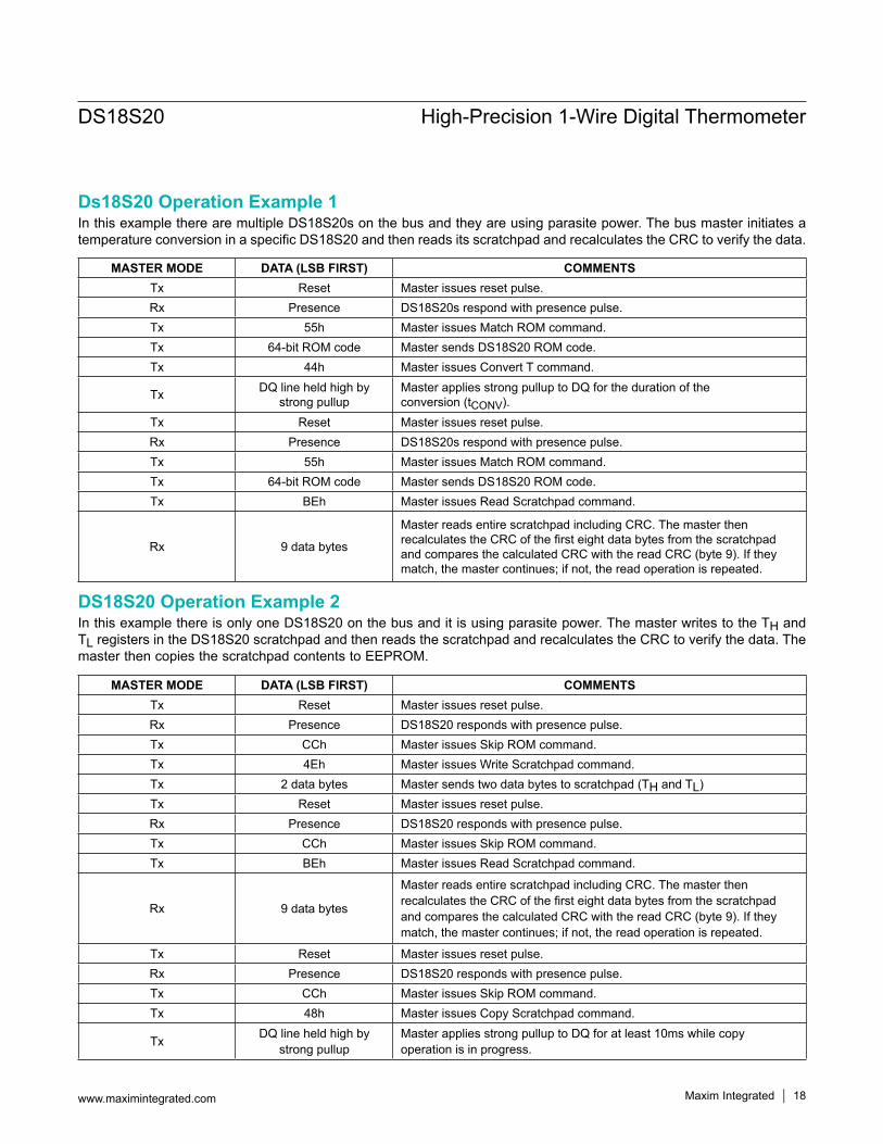
Ds18S20 Operation Example 1In this example there are multiple DS18S20s on the bus and they are using parasite power. The bus master initiates a temperature conversion in a specific DS18S20 and then reads its scratchpad and recalculates the CRC to verify the data.
DS18S20 Operation Example 2In this example there is only one DS18S20 on the bus and it is using parasite power. The master writes to the TH and TL registers in the DS18S20 scratchpad and then reads the scratchpad and recalculates the CRC to verify the data. The master then copies the scratchpad contents to EEPROM.
MASTER MODE DATA (LSB FIRST) COMMENTSTx Reset Master issues reset pulse.Rx Presence DS18S20s respond with presence pulse.Tx 55h Master issues Match ROM command.Tx 64-bit ROM code Master sends DS18S20 ROM code.Tx 44h Master issues Convert T command.
Tx DQ line held high by strong pullup
Master applies strong pullup to DQ for the duration of the conversion (tCONV).
Tx Reset Master issues reset pulse.Rx Presence DS18S20s respond with presence pulse.Tx 55h Master issues Match ROM command.Tx 64-bit ROM code Master sends DS18S20 ROM code.Tx BEh Master issues Read Scratchpad command.
Rx 9 data bytes
Master reads entire scratchpad including CRC. The master then recalculates the CRC of the first eight data bytes from the scratchpad and compares the calculated CRC with the read CRC (byte 9). If they match, the master continues; if not, the read operation is repeated.
MASTER MODE DATA (LSB FIRST) COMMENTSTx Reset Master issues reset pulse.Rx Presence DS18S20 responds with presence pulse.Tx CCh Master issues Skip ROM command.Tx 4Eh Master issues Write Scratchpad command.Tx 2 data bytes Master sends two data bytes to scratchpad (TH and TL)Tx Reset Master issues reset pulse.Rx Presence DS18S20 responds with presence pulse.Tx CCh Master issues Skip ROM command.Tx BEh Master issues Read Scratchpad command.
Rx 9 data bytes
Master reads entire scratchpad including CRC. The master then recalculates the CRC of the first eight data bytes from the scratchpad and compares the calculated CRC with the read CRC (byte 9). If they match, the master continues; if not, the read operation is repeated.
Tx Reset Master issues reset pulse.Rx Presence DS18S20 responds with presence pulse.Tx CCh Master issues Skip ROM command.Tx 48h Master issues Copy Scratchpad command.
Tx DQ line held high by strong pullup
Master applies strong pullup to DQ for at least 10ms while copy operation is in progress.
DS18S20 High-Precision 1-Wire Digital Thermometer
www.maximintegrated.com Maxim Integrated 18

DS18S20 Operation Example 3In this example there is only one DS18S20 on the bus and it is using parasite power. The bus master initiates a tempera-ture conversion then reads the DS18S20 scratchpad and calculates a higher resolution result using the data from the temperature, COUNT REMAIN and COUNT PER °C registers.
MASTER MODE DATA (LSB FIRST) COMMENTSTx Reset Master issues reset pulse.
Tx Presence DS18S20 responds with presence pulse.
Tx CCh Master issues Skip ROM command.
Tx 44h Master issues Convert T command.
Tx DQ line held high by strong pullup Master applies strong pullup to DQ for the duration of the conversion (tCONV).
Tx Reset Master issues reset pulse.
Rx Presence DS18S20 responds with presence pulse.
Tx CCh Master issues Skip ROM command.
Tx BEh Master issues Read Scratchpad command.
Rx 9 data bytes
Master reads entire scratchpad including CRC. The master then recalculates the CRC of the first eight data bytes from the scratchpad and compares the calculated CRC with the read CRC (byte 9). If they match, the master continues; if not, the read operation is repeated. The master also calculates the TEMP_READ value and stores the contents of the COUNT REMAIN and Count Per °C registers.
Tx Reset Master issues reset pulse.
Rx Presence DS18S20 responds with presence pulse.
— — CPU calculates extended resolution temperature using the equation inthe Operation—Measuring Temperature section.
DS18S20 High-Precision 1-Wire Digital Thermometer
www.maximintegrated.com Maxim Integrated 19

+Denotes a lead(Pb)-free/RoHS-compliant package. A “+” appears on the top mark of lead(Pb)-free packages.T&R = Tape and reel.*TO-92 packages in tape and reel can be ordered with straight or formed leads. Choose “SL” for straight leads. Bulk TO-92 orders are straight leads only.
PART TEMP RANGE PIN-PACKAGEDS18S20+ –55°C to +125°C 3 TO-92
DS18S20+T&R –55°C to +125°C 3 TO-92 (2000 Piece)
DS18S20-SL+T&R –55°C to +125°C 3 TO-92 (2000 Piece)*
DS18S20Z –55°C to +125°C 8 SO
DS18S20Z+ –55°C to +125°C 8 SO
DS18S20Z/T&R –55°C to +125°C 8 SO (2500 Piece)
DS18S20Z+T&R –55°C to +125°C 8 SO (2500 Piece)
PACKAGE TYPE
PACKAGE CODE
OUTLINE NO.
LAND PATTERN NO.
8 SO S8-2 21-0041 90-0096
3 TO-92 (straight leads) Q3-1 21-0248 —
3 TO-92 (formed leads) Q3-4 21-0250 —
DS18S20 High-Precision 1-Wire Digital Thermometer
www.maximintegrated.com Maxim Integrated 20
Ordering Information Package InformationFor the latest package outline information and land patterns (footprints), go to www.maximintegrated.com/packages. Note that a “+”, “#”, or “-” in the package code indicates RoHS status only. Package drawings may show a different suffix character, but the drawing pertains to the package regardless of RoHS status.

REVISION NUMBER
REVISION DATE DESCRIPTION PAGES
CHANGED
0 4/08In the Ordering Information table, added TO-92 straight-lead packages and included a note that the TO-92 package in tape and reel can be ordered with either formed or straight leads
2
1 8/10Removed the Top Mark column from the Ordering Information table; added the continuous power dissipation and lead and soldering temperatures to the Absolute Maximum Ratings section
2, 20
2 1/15 Updated General Description and Benefits and Features section and added Applications section 1
3 4/15 Revised Pin Configuration and Ordering Information 1, 20
Maxim Integrated cannot assume responsibility for use of any circuitry other than circuitry entirely embodied in a Maxim Integrated product. No circuit patent licenses are implied. Maxim Integrated reserves the right to change the circuitry and specifications without notice at any time. The parametric values (min and max limits) shown in the Electrical Characteristics table are guaranteed. Other parametric values quoted in this data sheet are provided for guidance.
Maxim Integrated and the Maxim Integrated logo are trademarks of Maxim Integrated Products, Inc. © 2015 Maxim Integrated Products, Inc. 21
DS18S20 High-Precision 1-Wire Digital Thermometer
Revision History
For pricing, delivery, and ordering information, please contact Maxim Direct at 1-888-629-4642, or visit Maxim Integrated’s website at www.maximintegrated.com.