Embed Size (px)
Citation preview
DS2482-100 Single-Channel 1-Wire Master
General DescriptionThe DS2482-100 is an I2C-to-1-Wire® bridge devicethat interfaces directly to standard (100kHz max) or fast(400kHz max) I2C masters to perform bidirectional pro-tocol conversion between the I2C master and anydownstream 1-Wire slave devices. Relative to anyattached 1-Wire slave device, the DS2482-100 is a1-Wire master. Internal, factory-trimmed timers relievethe system host processor from generating time-critical1-Wire waveforms, supporting both standard and over-drive 1-Wire communication speeds. To optimize1-Wire waveform generation, the DS2482-100 performsslew-rate control on rising and falling 1-Wire edges andprovides additional programmable features to matchdrive characteristics to the 1-Wire slave environment.Programmable, strong pullup features support 1-Wirepower delivery to 1-Wire devices such as EEPROMsand sensors. The DS2482-100 combines these featureswith an output to control an external MOSFET forenhanced strong pullup application. The I2C slaveaddress assignment is controlled by two binaryaddress inputs, resolving potential conflicts with otherI2C slave devices in the system.
Applications
Benefits and Features• Allows Easy Interface Between a I2C Microport and a
1-Wire Slave• I2C Host Interface Supports 100kHz and 400kHz
I2C Communication Speeds• 1-Wire Master IO with Selectable Active or Passive
1-Wire Pullup• Provides Reset/Presence, 8-Bit, Single-Bit, and
3-Bit 1-Wire IO Sequences• Standard and Overdrive 1-Wire Communication
Speeds• Two Address Inputs for I2C Address Assignment
• Minimizes Line Noise Reducing System EMI• Slew-Controlled 1-Wire Edges
• Supports EEPROMs, Temperature Sensors, or Other 1-Wire Slaves That Have Momentary High Source Current Modes• Strong 1-Wire Pullup Provided by an Internal Low-
Impedance Signal Path• PCTLZ Output to Optionally Control an External
MOSFET for Stronger Pullup Requirements• Operating Range: 2.9V to 5.5V, -40°C to +85°C
• 8-Pin (150 mils) SO and 9-Bump WLP Packages
19-4930; Rev 10; 1/15
Printers
Medical Instruments
Industrial Sensors
Cell Phones, PDAs
Typical Operating Circuit
1-Wire is a registered trademark of Maxim Integrated Products, Inc.
DS2482-100
SDASCL
AD1AD0
PCTLZ
IO
RP*
*RP = I2C PULLUP RESISTOR (SEE THE APPLICATIONS INFORMATION SECTION FOR RP SIZING).
VCC
CURRENT-LIMITINGRESISTORREFER TO APPLICATIONNOTE 4206
OPTIONALCIRCUITRY
1-Wire LINE
µC
(I2C PORT)
1-WireDEVICE
1-WireDEVICE
1-WireDEVICE
Pin Configurations and Ordering Information appear at end of data sheet.
Maxim Integrated | 2www.maximintegrated.com
DS2482-100 Single-Channel 1-Wire Master
Absolute Maximum Ratings
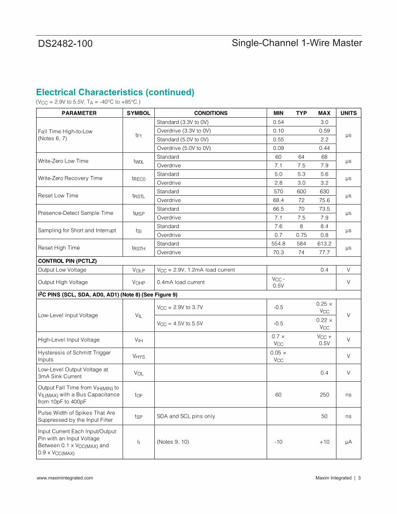
Electrical Characteristics(VCC = 2.9V to 5.5V, TA = -40°C to +85°C.)
Stresses beyond those listed under “Absolute Maximum Ratings” may cause permanent damage to the device. These are stress ratings only, and functionaloperation of the device at these or any other conditions beyond those indicated in the operational sections of the specifications is not implied. Exposure toabsolute maximum rating conditions for extended periods may affect device reliability.
Voltage Range on Any Pin Relative to Ground.........-0.5V to +6VMaximum Current into Any Pin .........................................±20mAOperating Temperature Range ...........................-40°C to +85°CJunction Temperature ......................................................+150°C
Storage Temperature Range .............................-55°C to +125°CLead Temperature (SO only; soldering, 10s)...................+300°CSoldering Temperature (reflow)
SO, WLP.......................................................................+260°C
PARAMETER SYMBOL CONDITIONS MIN TYP MAX UNITS
3.3V 2.9 3.3 3.7 Supply Voltage VCC
5V 4.5 5.0 5.5 V
Operating Current ICC (Note 1) 0.75 mA
3.3V 1.9 1-Wire Input High (Notes 2, 3) VIH1
5V 3.4 V
3.3V 0.9 1-Wire Input Low (Notes 2, 3) VIL1
5V 1.2 V
1-Wire Weak Pullup Resistor RWPU (Note 4) 1000 1675
1-Wire Output Low VOL1 At 4mA load 0.4 V
Standard 2.3 2.5 2.7 Active Pullup On Time (Notes 4, 5)
tAPUOT Overdrive 0.4 0.5 0.6
μs
VCC 3.2V, 1.5mA load 0.3 Strong Pullup Voltage Drop VSTRPU
VCC 5.2V, 3mA load 0.5 V
Standard (3.3V ±10%) 1 4.2
Overdrive (3.3V ±10%) 5 22.1
Standard (5.0V ±10%) 2 6.5 Pulldown Slew Rate (Note 6) PDSRC
Overdrive (5.0V ±10%) 10 40
V/μs
Standard (3.3V ±10%) 0.8 4
Overdrive (3.3V ±10%) 2.7 20
Standard (5.0V ±10%) 1.3 6 Pullup Slew Rate (Note 6) PUSRC
Overdrive (5.0V ±10%) 3.4 31
V/μs
Power-On Reset Trip Point VPOR 2.2 V
1-Wire TIMING (Note 5) (See Figures 4, 5, and 6)
Standard 7.6 8 8.4 Write-One/Read Low Time tW1L
Overdrive 0.9 1 1.1 μs
Standard 13.3 14 15 Read Sample Time tMSR
Overdrive 1.4 1.5 1.8 μs
Standard 65.8 69.3 72.8 1-Wire Time Slot tSLOT
Overdrive 9.9 10.5 11.0 μs
Maxim Integrated | 3www.maximintegrated.com
DS2482-100 Single-Channel 1-Wire Master
PARAMETER SYMBOL CONDITIONS MIN TYP MAX UNITS
Standard (3.3V to 0V) 0.54 3.0
Overdrive (3.3V to 0V) 0.10 0.59
Standard (5.0V to 0V) 0.55 2.2 Fall Time High-to-Low (Notes 6, 7)
tF1
Overdrive (5.0V to 0V) 0.09 0.44
μs
Standard 60 64 68 Write-Zero Low Time tW0L
Overdrive 7.1 7.5 7.9 μs
Standard 5.0 5.3 5.6 Write-Zero Recovery Time tREC0
Overdrive 2.8 3.0 3.2 μs
Standard 570 600 630 Reset Low Time tRSTL
Overdrive 68.4 72 75.6μs
Standard 66.5 70 73.5Presence-Detect Sample Time tMSP
Overdrive 7.1 7.5 7.9 μs
Standard 7.6 8 8.4Sampling for Short and Interrupt tSI
Overdrive 0.7 0.75 0.8 μs
Standard 554.8 584 613.2Reset High Time tRSTH
Overdrive 70.3 74 77.7μs
CONTROL PIN (PCTLZ)
Output Low Voltage VOLP VCC = 2.9V, 1.2mA load current 0.4 V
Output High Voltage VOHP 0.4mA load current VCC - 0.5V
V
I2C PINS (SCL, SDA, AD0, AD1) (Note 8) (See Figure 9)
VCC = 2.9V to 3.7V -0.5 0.25 ×
VCC Low-Level Input Voltage VIL
VCC = 4.5V to 5.5V -0.5 0.22 ×
VCC
V
High-Level Input Voltage VIH0.7 × VCC
VCC + 0.5V
V
Hysteresis of Schmitt Trigger Inputs
VHYS0.05 ×
VCC V
Low-Level Output Voltage at 3mA Sink Current
VOL 0.4 V
Output Fall Time from VIH(MIN) to VIL(MAX) with a Bus Capacitance from 10pF to 400pF
tOF 60 250 ns
Pulse Width of Spikes That Are Suppressed by the Input Filter
tSP SDA and SCL pins only 50 ns
Input Current Each Input/Output Pin with an Input Voltage Between 0.1 x VCC(MAX) and 0.9 x VCC(MAX)
II (Notes 9, 10) -10 +10 μA
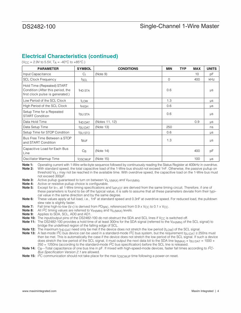
Electrical Characteristics (continued)(VCC = 2.9V to 5.5V, TA = -40°C to +85°C.)
Maxim Integrated | 4www.maximintegrated.com
DS2482-100 Single-Channel 1-Wire Master
Note 1: Operating current with 1-Wire write-byte sequence followed by continuously reading the Status Register at 400kHz in overdrive.Note 2: With standard speed, the total capacitive load of the 1-Wire bus should not exceed 1nF. Otherwise, the passive pullup on
threshold VIL1 may not be reached in the available time. With overdrive speed, the capacitive load on the 1-Wire bus mustnot exceed 300pF.
Note 3: Active pullup guaranteed to turn on between VIL1(MAX) and VIH1(MIN).Note 4: Active or resistive pullup choice is configurable.Note 5: Except for tF1, all 1-Wire timing specifications and tAPUOT are derived from the same timing circuit. Therefore, if one of
these parameters is found to be off the typical value, it is safe to assume that all these parameters deviate from their typi-cal value in the same direction and by the same degree.
Note 6: These values apply at full load, i.e., 1nF at standard speed and 0.3nF at overdrive speed. For reduced load, the pulldownslew rate is slightly faster.
Note 7: Fall time high-to-low (tF1) is derived from PDSRC, referenced from 0.9 x VCC to 0.1 x VCC.Note 8: All I2C timing values are referred to VIH(MIN) and VIL(MAX) levels.Note 9: Applies to SDA, SCL, AD0 and AD1.Note 10: The input/output pins of the DS2482-100 do not obstruct the SDA and SCL lines if VCC is switched off.Note 11: The DS2482-100 provides a hold time of at least 300ns for the SDA signal (referred to the VIH(MIN) of the SCL signal) to
bridge the undefined region of the falling edge of SCL.Note 12: The maximum tHD:DAT need only be met if the device does not stretch the low period (tLOW) of the SCL signal.Note 13: A fast-mode I2C bus device can be used in a standard-mode I2C bus system, but the requirement tSU:DAT ≥ 250ns must
then be met. This is automatically the case if the device does not stretch the low period of the SCL signal. If such a devicedoes stretch the low period of the SCL signal, it must output the next data bit to the SDA line tR(MAX) + tSU:DAT = 1000 +250 = 1250ns (according to the standard-mode I2C bus specification) before the SCL line is released.
Note 14: CB—Total capacitance of one bus line in pF. If mixed with high-speed-mode devices, faster fall times according to I2C-Bus Specification Version 2.1 are allowed.
Note 15: I2C communication should not take place for the max tOSCWUP time following a power-on reset.
Electrical Characteristics (continued)(VCC = 2.9V to 5.5V, TA = -40°C to +85°C.)
PARAMETER SYMBOL CONDITIONS MIN TYP MAX UNITS
Input Capacitance CI (Note 9) 10 pF
SCL Clock Frequency fSCL 0 400 kHz
Hold Time (Repeated) START Condition (After this period, the first clock pulse is generated.)
tHD:STA 0.6 μs
Low Period of the SCL Clock tLOW 1.3 μs
High Period of the SCL Clock tHIGH 0.6 μs
Setup Time for a Repeated START Condition
tSU:STA 0.6 μs
Data Hold Time tHD:DAT (Notes 11, 12) 0.9 μs
Data Setup Time tSU:DAT (Note 13) 250 ns
Setup Time for STOP Condition tSU:STO 0.6 μs
Bus Free Time Between a STOP and START Condition
tBUF 1.3 μs
Capacitive Load for Each Bus Line
CB (Note 14) 400 pF
Oscillator Warmup Time tOSCWUP (Note 15) 100 μs
Maxim Integrated | 5www.maximintegrated.com
DS2482-100 Single-Channel 1-Wire Master
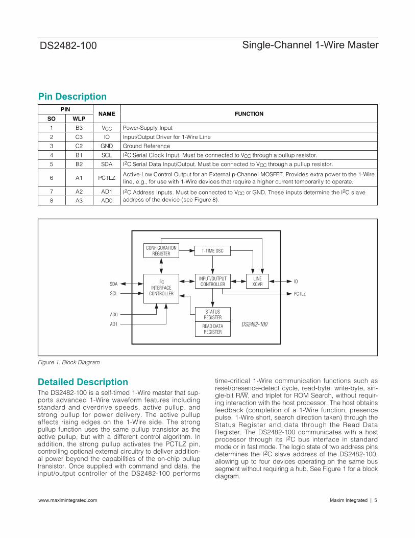
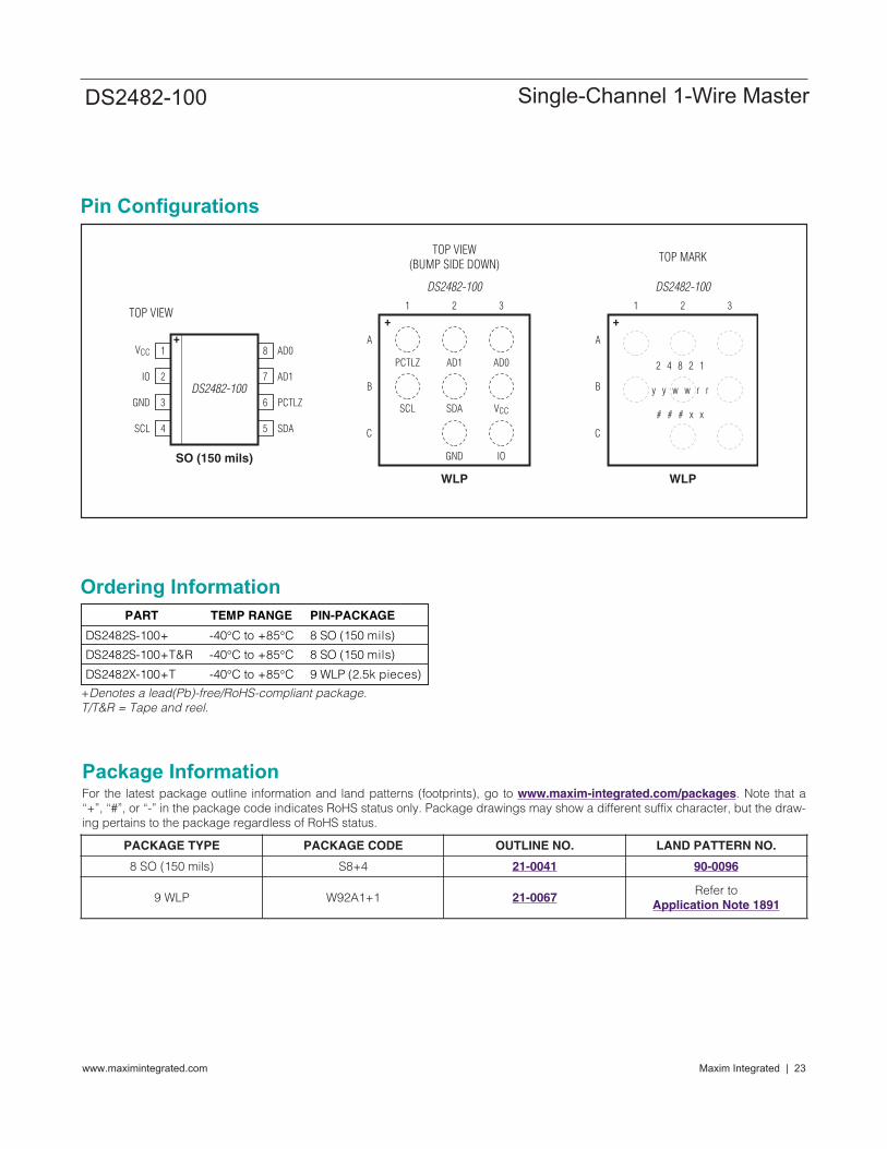
Pin Description
PIN
SO WLPNAME FUNCTION
1 B3 VCC Power-Supply Input
2 C3 IO Input/Output Driver for 1-Wire Line
3 C2 GND Ground Reference
4 B1 SCL I2C Serial Clock Input. Must be connected to VCC through a pullup resistor.
5 B2 SDA I2C Serial Data Input/Output. Must be connected to VCC through a pullup resistor.
6 A1 PCTLZ Active-Low Control Output for an External p-Channel MOSFET. Provides extra power to the 1-Wire line, e.g., for use with 1-Wire devices that require a higher current temporarily to operate.
7 A2 AD1
8 A3 AD0 I2C Address Inputs. Must be connected to VCC or GND. These inputs determine the I2C slave address of the device (see Figure 8).
CONFIGURATIONREGISTER
I2CINTERFACE
CONTROLLER
INPUT/OUTPUTCONTROLLER
LINEXCVR
T-TIME OSC
DS2482-100
STATUSREGISTER
READ DATAREGISTER
SDA IO
PCTLZ
AD0
AD1
SCL
Figure 1. Block Diagram
Detailed DescriptionThe DS2482-100 is a self-timed 1-Wire master that sup-ports advanced 1-Wire waveform features includingstandard and overdrive speeds, active pullup, andstrong pullup for power delivery. The active pullupaffects rising edges on the 1-Wire side. The strongpullup function uses the same pullup transistor as theactive pullup, but with a different control algorithm. Inaddition, the strong pullup activates the PCTLZ pin,controlling optional external circuitry to deliver addition-al power beyond the capabilities of the on-chip pulluptransistor. Once supplied with command and data, theinput/output controller of the DS2482-100 performs
time-critical 1-Wire communication functions such asreset/presence-detect cycle, read-byte, write-byte, sin-gle-bit R/W, and triplet for ROM Search, without requir-ing interaction with the host processor. The host obtainsfeedback (completion of a 1-Wire function, presencepulse, 1-Wire short, search direction taken) through theStatus Register and data through the Read DataRegister. The DS2482-100 communicates with a hostprocessor through its I2C bus interface in standardmode or in fast mode. The logic state of two address pinsdetermines the I2C slave address of the DS2482-100,allowing up to four devices operating on the same bussegment without requiring a hub. See Figure 1 for a blockdiagram.
Maxim Integrated | 6www.maximintegrated.com
DS2482-100 Single-Channel 1-Wire Master
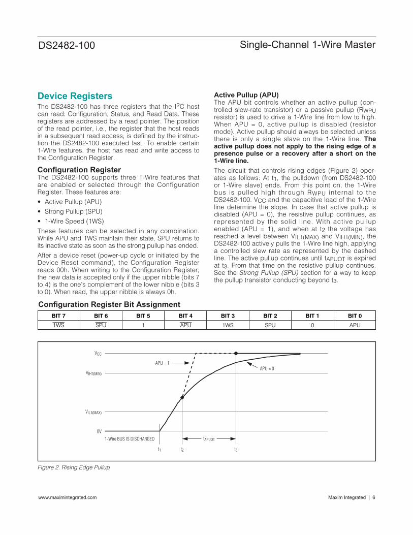
VCC
0V1-Wire BUS IS DISCHARGED
VIL1(MAX)
VIH1(MIN)
t1 t2
tAPUOT
t3
APU = 1APU = 0
Figure 2. Rising Edge Pullup
Configuration Register Bit Assignment
BIT 7 BIT 6 BIT 5 BIT 4 BIT 3 BIT 2 BIT 1 BIT 0
1WS SPU 1 APU 1WS SPU 0 APU
Device RegistersThe DS2482-100 has three registers that the I2C hostcan read: Configuration, Status, and Read Data. Theseregisters are addressed by a read pointer. The positionof the read pointer, i.e., the register that the host readsin a subsequent read access, is defined by the instruc-tion the DS2482-100 executed last. To enable certain1-Wire features, the host has read and write access tothe Configuration Register.
Configuration RegisterThe DS2482-100 supports three 1-Wire features thatare enabled or selected through the ConfigurationRegister. These features are:
• Active Pullup (APU)
• Strong Pullup (SPU)
• 1-Wire Speed (1WS)
These features can be selected in any combination.While APU and 1WS maintain their state, SPU returns toits inactive state as soon as the strong pullup has ended.
After a device reset (power-up cycle or initiated by theDevice Reset command), the Configuration Registerreads 00h. When writing to the Configuration Register,the new data is accepted only if the upper nibble (bits 7to 4) is the one’s complement of the lower nibble (bits 3to 0). When read, the upper nibble is always 0h.
Active Pullup (APU)The APU bit controls whether an active pullup (con-trolled slew-rate transistor) or a passive pullup (RWPUresistor) is used to drive a 1-Wire line from low to high.When APU = 0, active pullup is disabled (resistormode). Active pullup should always be selected unlessthere is only a single slave on the 1-Wire line. Theactive pullup does not apply to the rising edge of apresence pulse or a recovery after a short on the1-Wire line.
The circuit that controls rising edges (Figure 2) oper-ates as follows: At t1, the pulldown (from DS2482-100or 1-Wire slave) ends. From this point on, the 1-Wirebus is pulled high through RWPU internal to theDS2482-100. VCC and the capacitive load of the 1-Wireline determine the slope. In case that active pullup isdisabled (APU = 0), the resistive pullup continues, asrepresented by the solid line. With active pullupenabled (APU = 1), and when at t2 the voltage hasreached a level between VIL1(MAX) and VIH1(MIN), theDS2482-100 actively pulls the 1-Wire line high, applyinga controlled slew rate as represented by the dashedline. The active pullup continues until tAPUOT is expiredat t3. From that time on the resistive pullup continues.See the Strong Pullup (SPU) section for a way to keepthe pullup transistor conducting beyond t3.
Maxim Integrated | 7www.maximintegrated.com
DS2482-100 Single-Channel 1-Wire Master
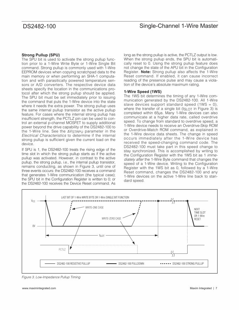
Strong Pullup (SPU)The SPU bit is used to activate the strong pullup func-tion prior to a 1-Wire Write Byte or 1-Wire Single Bitcommand. Strong pullup is commonly used with 1-WireEEPROM devices when copying scratchpad data to themain memory or when performing an SHA-1 computa-tion and with parasitically powered temperature sen-sors or A/D converters. The respective device datasheets specify the location in the communications pro-tocol after which the strong pullup should be applied.The SPU bit must be set immediately prior to issuingthe command that puts the 1-Wire device into the statewhere it needs the extra power. The strong pullup usesthe same internal pullup transistor as the active pullupfeature. For cases where the internal strong pullup hasinsufficient strength, the PCTLZ pin can be used to con-trol an external p-channel MOSFET to supply additionalpower beyond the drive capability of the DS2482-100 tothe 1-Wire line. See the ΔVSTRPU parameter in theElectrical Characteristics to determine if the internalstrong pullup is sufficient given the current load on thedevice.
If SPU is 1, the DS2482-100 treats the rising edge of thetime slot in which the strong pullup starts as if the activepullup was activated. However, in contrast to the activepullup, the strong pullup, i.e., the internal pullup transistor,remains conducting, as shown in Figure 3, until one ofthree events occurs: the DS2482-100 receives a commandthat generates 1-Wire communication (the typical case);the SPU bit in the Configuration Register is written to 0; orthe DS2482-100 receives the Device Reset command. As
long as the strong pullup is active, the PCTLZ output is low.When the strong pullup ends, the SPU bit is automati-cally reset to 0. Using the strong pullup feature doesnot change the state of the APU bit in the ConfigurationRegister. Note: Strong pullup also affects the 1-WireReset command. If enabled, it can cause incorrectreading of the presence pulse and may cause a viola-tion of the device’s absolute maximum rating.
1-Wire Speed (1WS)The 1WS bit determines the timing of any 1-Wire com-munication generated by the DS2482-100. All 1-Wireslave devices support standard speed (1WS = 0),where the transfer of a single bit (tSLOT in Figure 3) iscompleted within 65µs. Many 1-Wire devices can alsocommunicate at a higher data rate, called overdrivespeed. To change from standard to overdrive speed, a1-Wire device needs to receive an Overdrive-Skip ROMor Overdrive-Match ROM command, as explained inthe 1-Wire device data sheets. The change in speedoccurs immediately after the 1-Wire device hasreceived the speed-changing command code. TheDS2482-100 must take part in this speed change tostay synchronized. This is accomplished by writing tothe Configuration Register with the 1WS bit as 1 imme-diately after the 1-Wire Byte command that changes thespeed of a 1-Wire device. Writing to the ConfigurationRegister with the 1WS bit as 0, followed by a 1-WireReset command, changes the DS2482-100 and any1-Wire devices on the active 1-Wire line back to stan-dard speed.
DS2482-100 RESISTIVE PULLUP DS2482-100 PULLDOWN DS2482-100 STRONG PULLUP
VCC
0V
PCTLZ
WRITE-ZERO CASE
WRITE-ONE CASE
tSLOT
LAST BIT OF 1-Wire WRITE BYTE OR 1-Wire SINGLE BIT FUNCTION
NEXTTIME SLOTOR 1-WireRESET
Figure 3. Low-Impedance Pullup Timing
Maxim Integrated | 8www.maximintegrated.com
DS2482-100 Single-Channel 1-Wire Master
Status RegisterThe read-only Status Register is the general means forthe DS2482-100 to report bit-type data from the 1-Wireside, 1-Wire busy status, and its own reset status to thehost processor. All 1-Wire communication commandsand the Device Reset command position the readpointer at the Status Register for the host processor toread with minimal protocol overhead. Status informationis updated during the execution of certain commandsonly. Details are given in the description of the variousstatus bits that follow.
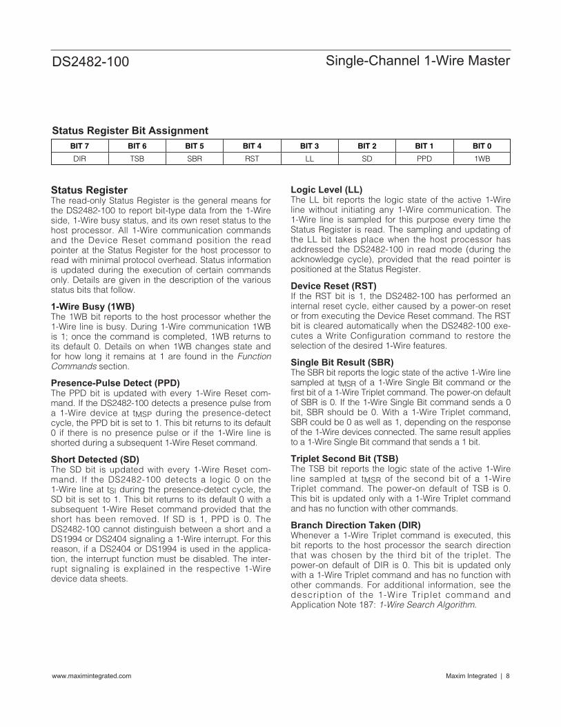
1-Wire Busy (1WB)The 1WB bit reports to the host processor whether the1-Wire line is busy. During 1-Wire communication 1WBis 1; once the command is completed, 1WB returns toits default 0. Details on when 1WB changes state andfor how long it remains at 1 are found in the FunctionCommands section.
Presence-Pulse Detect (PPD)The PPD bit is updated with every 1-Wire Reset com-mand. If the DS2482-100 detects a presence pulse froma 1-Wire device at tMSP during the presence-detectcycle, the PPD bit is set to 1. This bit returns to its default0 if there is no presence pulse or if the 1-Wire line isshorted during a subsequent 1-Wire Reset command.
Short Detected (SD)The SD bit is updated with every 1-Wire Reset com-mand. If the DS2482-100 detects a logic 0 on the1-Wire line at tSI during the presence-detect cycle, theSD bit is set to 1. This bit returns to its default 0 with asubsequent 1-Wire Reset command provided that theshort has been removed. If SD is 1, PPD is 0. TheDS2482-100 cannot distinguish between a short and aDS1994 or DS2404 signaling a 1-Wire interrupt. For thisreason, if a DS2404 or DS1994 is used in the applica-tion, the interrupt function must be disabled. The inter-rupt signaling is explained in the respective 1-Wiredevice data sheets.
Logic Level (LL)The LL bit reports the logic state of the active 1-Wireline without initiating any 1-Wire communication. The1-Wire line is sampled for this purpose every time theStatus Register is read. The sampling and updating ofthe LL bit takes place when the host processor hasaddressed the DS2482-100 in read mode (during theacknowledge cycle), provided that the read pointer ispositioned at the Status Register.
Device Reset (RST)If the RST bit is 1, the DS2482-100 has performed aninternal reset cycle, either caused by a power-on resetor from executing the Device Reset command. The RSTbit is cleared automatically when the DS2482-100 exe-cutes a Write Configuration command to restore theselection of the desired 1-Wire features.
Single Bit Result (SBR)The SBR bit reports the logic state of the active 1-Wire linesampled at tMSR of a 1-Wire Single Bit command or thefirst bit of a 1-Wire Triplet command. The power-on defaultof SBR is 0. If the 1-Wire Single Bit command sends a 0bit, SBR should be 0. With a 1-Wire Triplet command,SBR could be 0 as well as 1, depending on the responseof the 1-Wire devices connected. The same result appliesto a 1-Wire Single Bit command that sends a 1 bit.
Triplet Second Bit (TSB)The TSB bit reports the logic state of the active 1-Wireline sampled at tMSR of the second bit of a 1-WireTriplet command. The power-on default of TSB is 0.This bit is updated only with a 1-Wire Triplet commandand has no function with other commands.
Branch Direction Taken (DIR)Whenever a 1-Wire Triplet command is executed, thisbit reports to the host processor the search directionthat was chosen by the third bit of the triplet. Thepower-on default of DIR is 0. This bit is updated onlywith a 1-Wire Triplet command and has no function withother commands. For additional information, see thedescription of the 1-Wire Triplet command andApplication Note 187: 1-Wire Search Algorithm.
Status Register Bit Assignment
BIT 7 BIT 6 BIT 5 BIT 4 BIT 3 BIT 2 BIT 1 BIT 0
DIR TSB SBR RST LL SD PPD 1WB
Maxim Integrated | 9www.maximintegrated.com
DS2482-100 Single-Channel 1-Wire Master
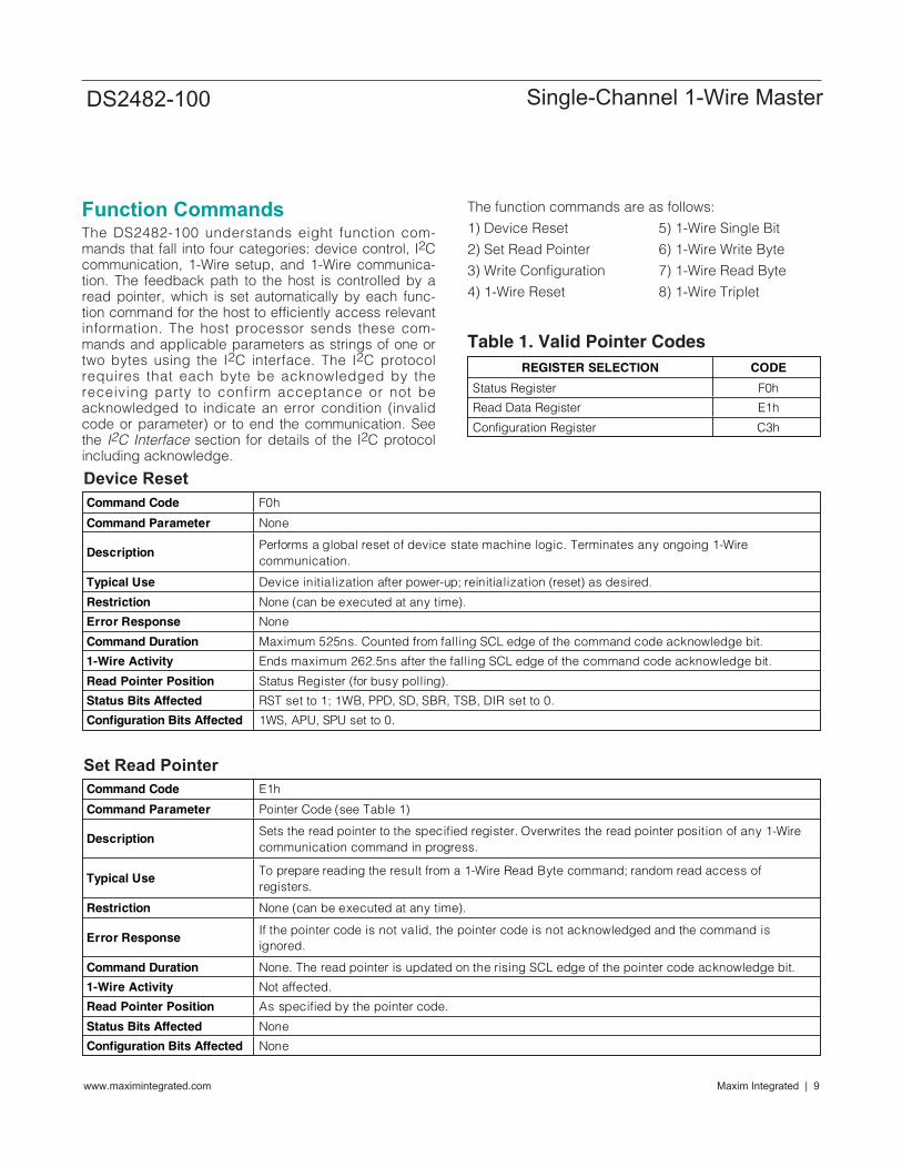
Function CommandsThe DS2482-100 understands eight function com-mands that fall into four categories: device control, I2Ccommunication, 1-Wire setup, and 1-Wire communica-tion. The feedback path to the host is controlled by aread pointer, which is set automatically by each func-tion command for the host to efficiently access relevantinformation. The host processor sends these com-mands and applicable parameters as strings of one ortwo bytes using the I2C interface. The I2C protocolrequires that each byte be acknowledged by thereceiving party to confirm acceptance or not beacknowledged to indicate an error condition (invalidcode or parameter) or to end the communication. Seethe I2C Interface section for details of the I2C protocolincluding acknowledge.
The function commands are as follows:
1) Device Reset 5) 1-Wire Single Bit
2) Set Read Pointer 6) 1-Wire Write Byte
3) Write Configuration 7) 1-Wire Read Byte
4) 1-Wire Reset 8) 1-Wire Triplet
Table 1. Valid Pointer Codes
Device Reset
Command Code F0h
Command Parameter None
Description Performs a global reset of device state machine logic. Terminates any ongoing 1-Wire communication.
Typical Use Device initialization after power-up; reinitialization (reset) as desired.
Restriction None (can be executed at any time).
Error Response None
Command Duration Maximum 525ns. Counted from falling SCL edge of the command code acknowledge bit.
1-Wire Activity Ends maximum 262.5ns after the falling SCL edge of the command code acknowledge bit.
Read Pointer Position Status Register (for busy polling).
Status Bits Affected RST set to 1; 1WB, PPD, SD, SBR, TSB, DIR set to 0.
Configuration Bits Affected 1WS, APU, SPU set to 0.
Set Read Pointer
Command Code E1h
Command Parameter Pointer Code (see Table 1)
Description Sets the read pointer to the specified register. Overwrites the read pointer position of any 1-Wire communication command in progress.
Typical Use To prepare reading the result from a 1-Wire Read Byte command; random read access of registers.
Restriction None (can be executed at any time).
Error Response If the pointer code is not valid, the pointer code is not acknowledged and the command is ignored.
Command Duration None. The read pointer is updated on the rising SCL edge of the pointer code acknowledge bit.
1-Wire Activity Not affected.
Read Pointer Position As specified by the pointer code.
Status Bits Affected None
Configuration Bits Affected None
REGISTER SELECTION CODE
Status Register F0h
Read Data Register E1h
Configuration Register C3h
Maxim Integrated | 10www.maximintegrated.com
DS2482-100 Single-Channel 1-Wire Master
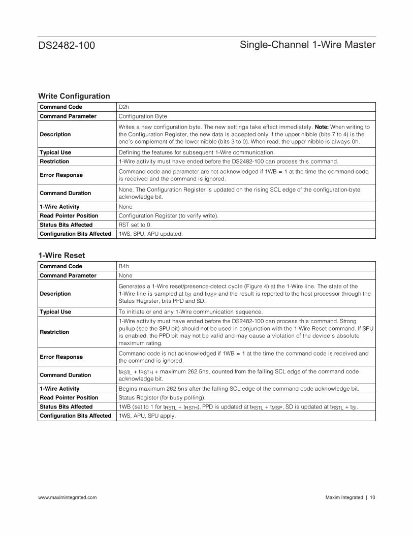
Write Configuration
Command Code D2h
Command Parameter Configuration Byte
Description Writes a new configuration byte. The new settings take effect immediately. Note: When writing to the Configuration Register, the new data is accepted only if the upper nibble (bits 7 to 4) is the one’s complement of the lower nibble (bits 3 to 0). When read, the upper nibble is always 0h.
Typical Use Defining the features for subsequent 1-Wire communication.
Restriction 1-Wire activity must have ended before the DS2482-100 can process this command.
Error Response Command code and parameter are not acknowledged if 1WB = 1 at the time the command code is received and the command is ignored.
Command Duration None. The Configuration Register is updated on the rising SCL edge of the configuration-byte acknowledge bit.
1-Wire Activity None
Read Pointer Position Configuration Register (to verify write).
Status Bits Affected RST set to 0.
Configuration Bits Affected 1WS, SPU, APU updated.
1-Wire Reset
Command Code B4h
Command Parameter None
Description Generates a 1-Wire reset/presence-detect cycle (Figure 4) at the 1-Wire line. The state of the 1-Wire line is sampled at tSI and tMSP and the result is reported to the host processor through the Status Register, bits PPD and SD.
Typical Use To initiate or end any 1-Wire communication sequence.
Restriction
1-Wire activity must have ended before the DS2482-100 can process this command. Strong pullup (see the SPU bit) should not be used in conjunction with the 1-Wire Reset command. If SPU is enabled, the PPD bit may not be valid and may cause a violation of the device’s absolute maximum rating.
Error Response Command code is not acknowledged if 1WB = 1 at the time the command code is received and the command is ignored.
Command Duration tRSTL + tRSTH + maximum 262.5ns, counted from the falling SCL edge of the command code acknowledge bit.
1-Wire Activity Begins maximum 262.5ns after the falling SCL edge of the command code acknowledge bit.
Read Pointer Position Status Register (for busy polling).
Status Bits Affected 1WB (set to 1 for tRSTL + tRSTH), PPD is updated at tRSTL + tMSP, SD is updated at tRSTL + tSI.
Configuration Bits Affected 1WS, APU, SPU apply.

Maxim Integrated | 11www.maximintegrated.com
DS2482-100 Single-Channel 1-Wire Master
PULLUP DS2482-100 PULLDOWN 1-Wire SLAVE PULLDOWN
VCC
VIH1
VIL1
0V
RESET PULSE
RESISTIVE PULLUP
PRESENCE PULSE
APU CONTROLLEDEDGE
PRESENCE/SHORT DETECT
tRSTL
tSItMSP
tRSTH
tF1
Figure 4. 1-Wire Reset/Presence-Detect Cycle
1-Wire Single Bit
Command Code 87h
Command Parameter Bit Byte
Description
Generates a single 1-Wire time slot with a bit value “V” as specified by the bit byte at the 1-Wire line (see Table 2). A V value of 0b generates a write-zero time slot (Figure 5); a V value of 1b generates a write-one time slot, which also functions as a read-data time slot (Figure 6). In either case, the logic level at the 1-Wire line is tested at tMSR and SBR is updated.
Typical Use To perform single-bit writes or reads at the 1-Wire line when single bit communication is necessary (the exception).
Restriction 1-Wire activity must have ended before the DS2482-100 can process this command.
Error Response Command code and bit byte are not acknowledged if 1WB = 1 at the time the command code is received and the command is ignored.
Command Duration tSLOT + maximum 262.5ns, counted from the falling SCL edge of the first bit (MSB) of the bit byte.
1-Wire Activity Begins maximum 262.5ns after the falling SCL edge of the MSB of the bit byte.
Read Pointer Position Status Register (for busy polling and data reading).
Status Bits Affected 1WB (set to 1 for tSLOT), SBR is updated at tMSR, DIR (may change its state).
Configuration Bits Affected 1WS, APU, SPU apply.
Table 2. Bit Allocation in the Bit ByteBIT 7 BIT 6 BIT 5 BIT 4 BIT 3 BIT 2 BIT 1 BIT 0
V x x x x x x x
x = Don’t care.

Maxim Integrated | 12www.maximintegrated.com
DS2482-100 Single-Channel 1-Wire Master
PULLUP (SEE FIGURE 2) DS2482-100 PULLDOWN
VCC
VIH1
VIL1
0V
tSLOT
tREC0
tWOLtMSR
tF1
Figure 5. Write-Zero Time Slot
PULLUP (SEE FIGURE 2) DS2482-100 PULLDOWN 1-Wire SLAVE PULLDOWN
VCC
VIH1
VIL1
0V
tSLOT
tW1L
tMSR
tF1
NOTE: DEPENDING ON ITS INTERNAL STATE, A 1-Wire SLAVE DEVICE TRANSMITS DATA TO ITS MASTER (e.g. THE DS2482-100). WHEN RESPONDING WITH A 0,A 1-Wire SLAVE STARTS PULLING THE LINE LOW DURING tW1L. ITS INTERNAL TIMING GENERATOR DETERMINES WHEN THIS PULLDOWN ENDS AND THE VOLTAGESTARTS RISING AGAIN. WHEN RESPONDING WITH A 1, A 1-Wire SLAVE DOES NOT HOLD THE LINE LOW AT ALL, AND THE VOLTAGE STARTS RISING AS SOON AS tW1LIS OVER. 1-Wire DEVICE DATA SHEETS USE THE TERM tRL INSTEAD OF tW1L TO DESCRIBE A READ-DATA TIME SLOT. TECHNICALLY, tRL AND tW1L HAVE IDENTICALSPECIFICATIONS AND CANNOT BE DISTINGUISHED FROM EACH OTHER.
Figure 6. Write-One and Read-Data Time Slot
Maxim Integrated | 13www.maximintegrated.com
DS2482-100 Single-Channel 1-Wire Master
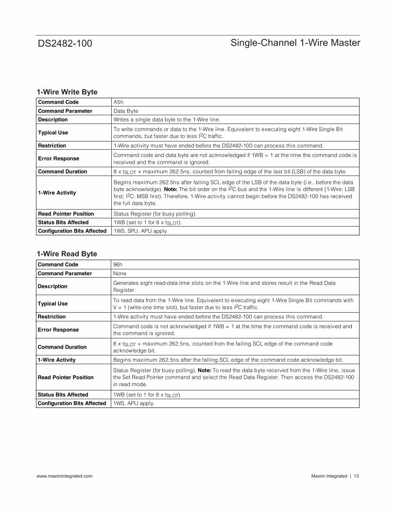
1-Wire Write Byte
Command Code A5h
Command Parameter Data Byte
Description Writes a single data byte to the 1-Wire line.
Typical Use To write commands or data to the 1-Wire line. Equivalent to executing eight 1-Wire Single Bit commands, but faster due to less I2C traffic.
Restriction 1-Wire activity must have ended before the DS2482-100 can process this command.
Error Response Command code and data byte are not acknowledged if 1WB = 1 at the time the command code is received and the command is ignored.
Command Duration 8 x tSLOT + maximum 262.5ns, counted from falling edge of the last bit (LSB) of the data byte.
1-Wire Activity
Begins maximum 262.5ns after falling SCL edge of the LSB of the data byte (i.e., before the data byte acknowledge). Note: The bit order on the I2C bus and the 1-Wire line is different (1-Wire: LSB first; I2C: MSB first). Therefore, 1-Wire activity cannot begin before the DS2482-100 has received the full data byte.
Read Pointer Position Status Register (for busy polling).
Status Bits Affected 1WB (set to 1 for 8 x tSLOT).
Configuration Bits Affected 1WS, SPU, APU apply.
1-Wire Read Byte
Command Code 96h
Command Parameter None
Description Generates eight read-data time slots on the 1-Wire line and stores result in the Read Data Register.
Typical Use To read data from the 1-Wire line. Equivalent to executing eight 1-Wire Single Bit commands with V = 1 (write-one time slot), but faster due to less I2C traffic.
Restriction 1-Wire activity must have ended before the DS2482-100 can process this command.
Error Response Command code is not acknowledged if 1WB = 1 at the time the command code is received and the command is ignored.
Command Duration 8 x tSLOT + maximum 262.5ns, counted from the falling SCL edge of the command code acknowledge bit.
1-Wire Activity Begins maximum 262.5ns after the falling SCL edge of the command code acknowledge bit.
Read Pointer Position Status Register (for busy polling). Note: To read the data byte received from the 1-Wire line, issue the Set Read Pointer command and select the Read Data Register. Then access the DS2482-100 in read mode.
Status Bits Affected 1WB (set to 1 for 8 x tSLOT).
Configuration Bits Affected 1WS, APU apply.
Maxim Integrated | 14www.maximintegrated.com
DS2482-100 Single-Channel 1-Wire Master
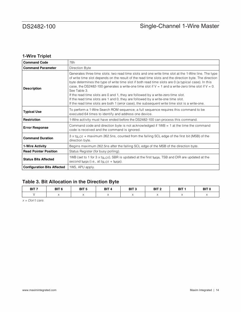
1-Wire Triplet
Command Code 78h
Command Parameter Direction Byte
Description
Generates three time slots: two read time slots and one write time slot at the 1-Wire line. The type of write time slot depends on the result of the read time slots and the direction byte. The direction byte determines the type of write time slot if both read time slots are 0 (a typical case). In this case, the DS2482-100 generates a write-one time slot if V = 1 and a write-zero time slot if V = 0. See Table 3. If the read time slots are 0 and 1, they are followed by a write-zero time slot. If the read time slots are 1 and 0, they are followed by a write-one time slot. If the read time slots are both 1 (error case), the subsequent write time slot is a write-one.
Typical Use To perform a 1-Wire Search ROM sequence; a full sequence requires this command to be executed 64 times to identify and address one device.
Restriction 1-Wire activity must have ended before the DS2482-100 can process this command.
Error Response Command code and direction byte is not acknowledged if 1WB = 1 at the time the command code is received and the command is ignored.
Command Duration 3 x tSLOT + maximum 262.5ns, counted from the falling SCL edge of the first bit (MSB) of the direction byte.
1-Wire Activity Begins maximum 262.5ns after the falling SCL edge of the MSB of the direction byte.
Read Pointer Position Status Register (for busy polling).
Status Bits Affected 1WB (set to 1 for 3 x tSLOT), SBR is updated at the first tMSR, TSB and DIR are updated at the second tMSR (i.e., at tSLOT + tMSR).
Configuration Bits Affected 1WS, APU apply.
Table 3. Bit Allocation in the Direction ByteBIT 7 BIT 6 BIT 5 BIT 4 BIT 3 BIT 2 BIT 1 BIT 0
V x x x x x x x
x = Don’t care.
Maxim Integrated | 15www.maximintegrated.com
DS2482-100 Single-Channel 1-Wire Master
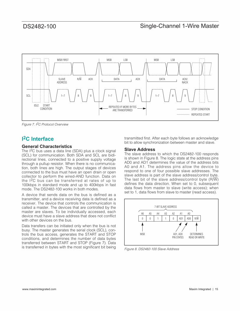
I2C Interface
General CharacteristicsThe I2C bus uses a data line (SDA) plus a clock signal(SCL) for communication. Both SDA and SCL are bidi-rectional lines, connected to a positive supply voltagethrough a pullup resistor. When there is no communica-tion, both lines are high. The output stages of devicesconnected to the bus must have an open drain or opencollector to perform the wired-AND function. Data onthe I2C bus can be transferred at rates of up to100kbps in standard mode and up to 400kbps in fastmode. The DS2482-100 works in both modes.
A device that sends data on the bus is defined as atransmitter, and a device receiving data is defined as areceiver. The device that controls the communication iscalled a master. The devices that are controlled by themaster are slaves. To be individually accessed, eachdevice must have a slave address that does not conflictwith other devices on the bus.
Data transfers can be initiated only when the bus is notbusy. The master generates the serial clock (SCL), con-trols the bus access, generates the START and STOPconditions, and determines the number of data bytestransferred between START and STOP (Figure 7). Datais transferred in bytes with the most significant bit being
transmitted first. After each byte follows an acknowledgebit to allow synchronization between master and slave.
Slave AddressThe slave address to which the DS2482-100 respondsis shown in Figure 8. The logic state at the address pinsAD0 and AD1 determines the value of the address bitsA0 and A1. The address pins allow the device torespond to one of four possible slave addresses. Theslave address is part of the slave address/control byte.The last bit of the slave address/control byte (R/W)defines the data direction. When set to 0, subsequentdata flows from master to slave (write access); whenset to 1, data flows from slave to master (read access).
SDA
SCL
IDLE
1–7 8 9 1–7 8 9 1–7 8 9
STARTCONDITION STOP CONDITION
REPEATED START
SLAVEADDRESS
R/W ACK ACKDATA ACK/NACK
DATA
MSB FIRST MSB LSB MSB LSB
REPEATED IF MORE BYTESARE TRANSFERRED
Figure 7. I2C Protocol Overview
Figure 8. DS2482-100 Slave Address
0
A6
MSB
0
A5
1
A4
1
A3
7-BIT SLAVE ADDRESS
0
A2
AD1
A1
AD0
A0
R/W
DETERMINESREAD OR WRITE
AD1, AD0PIN STATES
Maxim Integrated | 16www.maximintegrated.com
DS2482-100 Single-Channel 1-Wire Master
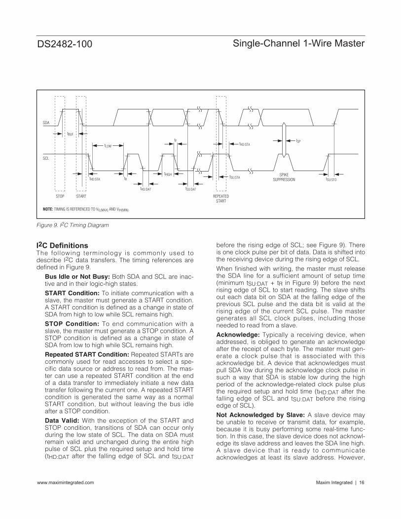
I2C DefinitionsThe following terminology is commonly used todescribe I2C data transfers. The timing references aredefined in Figure 9.
Bus Idle or Not Busy: Both SDA and SCL are inac-tive and in their logic-high states.
START Condition: To initiate communication with aslave, the master must generate a START condition.A START condition is defined as a change in state ofSDA from high to low while SCL remains high.
STOP Condition: To end communication with aslave, the master must generate a STOP condition. ASTOP condition is defined as a change in state ofSDA from low to high while SCL remains high.
Repeated START Condition: Repeated STARTs arecommonly used for read accesses to select a spe-cific data source or address to read from. The mas-ter can use a repeated START condition at the endof a data transfer to immediately initiate a new datatransfer following the current one. A repeated STARTcondition is generated the same way as a normalSTART condition, but without leaving the bus idleafter a STOP condition.
Data Valid: With the exception of the START andSTOP condition, transitions of SDA can occur onlyduring the low state of SCL. The data on SDA mustremain valid and unchanged during the entire highpulse of SCL plus the required setup and hold time(tHD:DAT after the falling edge of SCL and tSU:DAT
before the rising edge of SCL; see Figure 9). Thereis one clock pulse per bit of data. Data is shifted intothe receiving device during the rising edge of SCL.
When finished with writing, the master must releasethe SDA line for a sufficient amount of setup time(minimum tSU:DAT + tR in Figure 9) before the nextrising edge of SCL to start reading. The slave shiftsout each data bit on SDA at the falling edge of theprevious SCL pulse and the data bit is valid at therising edge of the current SCL pulse. The mastergenerates all SCL clock pulses, including thoseneeded to read from a slave.
Acknowledge: Typically a receiving device, whenaddressed, is obliged to generate an acknowledgeafter the receipt of each byte. The master must gen-erate a clock pulse that is associated with thisacknowledge bit. A device that acknowledges mustpull SDA low during the acknowledge clock pulse insuch a way that SDA is stable low during the highperiod of the acknowledge-related clock pulse plusthe required setup and hold time (tHD:DAT after thefalling edge of SCL and tSU:DAT before the risingedge of SCL).
Not Acknowledged by Slave: A slave device maybe unable to receive or transmit data, for example,because it is busy performing some real-time func-tion. In this case, the slave device does not acknowl-edge its slave address and leaves the SDA line high.A slave device that is ready to communicateacknowledges at least its slave address. However,
SCL
NOTE: TIMING IS REFERENCED TO VIL(MAX) AND VIH(MIN).
SDA
STOP START REPEATEDSTART
SPIKESUPPRESSION
tBUF
tHD:STA
tHD:DAT tSU:DAT
tSU:STO
tHD:STAtSP
tSU:STAtHIGH
tR
tFtLOW
Figure 9. I2C Timing Diagram

Maxim Integrated | 17www.maximintegrated.com
DS2482-100 Single-Channel 1-Wire Master
some time later the slave may refuse to accept data,possibly because of an invalid command code orparameter. In this case, the slave device does notacknowledge any of the bytes that it refuses andleaves SDA high. In either case, after a slave hasfailed to acknowledge, the master first should gener-ate a repeated START condition or a STOP conditionfollowed by a START condition to begin a new datatransfer.
Not Acknowledged by Master: At some time whenreceiving data, the master must signal an end ofdata to the slave device. To achieve this, the masterdoes not acknowledge the last byte that it hasreceived from the slave. In response, the slavereleases SDA, allowing the master to generate theSTOP condition.
Writing to the DS2482-100To write to the DS2482-100, the master must accessthe device in write mode, i.e., the slave address mustbe sent with the direction bit set to 0. The next byte tobe sent is a command code, which, depending on thecommand, may be followed by a command parameter.The DS2482-100 acknowledges valid command codesand expected/valid command parameters. Additionalbytes or invalid command parameters are neveracknowledged.
Reading from the DS2482-100To read from the DS2482-100, the master must accessthe device in read mode, i.e., the slave address mustbe sent with the direction bit set to 1. The read pointerdetermines the register that the master reads from. Themaster can continue reading the same register overand over again, without having to readdress the device,e.g., to watch the 1WB changing from 1 to 0. To readfrom a different register, the master must issue the SetRead Pointer command and then access the DS2482-100 again in read mode.
I2C Communication ExampleSee Tables 4 and 5 for the I2C communication legendand data direction codes.
Table 4. I2C Communication—LegendSYMBOL DESCRIPTION
S START Condition
AD, 0 Select DS2482-100 for Write Access
AD, 1 Select DS2482-100 for Read Access
Sr Repeated START Condition
P STOP Condition
A Acknowledged
A\ Not Acknowledged
(Idle) Bus Not Busy
<byte> Transfer of One Byte
DRST Command “Device Reset”, F0h
SRP Command “Set Read Pointer”, E1h
WCFG Command “Write Configuration”, D2h
1WRS Command “1-Wire Reset”, B4h
1WSB Command “1-Wire Single Bit”, 87h
1WWB Command “1-Wire Write Byte”, A5h
1WRB Command “1-Wire Read Byte”, 96h
1WT Command “1-Wire Triplet”, 78h
Table 5. Data Direction Codes
Master-to-Slave Slave-to-Master

Maxim Integrated | 18www.maximintegrated.com
DS2482-100 Single-Channel 1-Wire Master
Device Reset (After Power-Up)
Activities that are underlined denote an optional read access to verify the success of the command.
Set Read Pointer (To Read from Another Register)
Case A: Valid Read Pointer Code
C3h is the valid read pointer code for the Configuration Register.
Case B: Invalid Read Pointer Code
E5h is an invalid read pointer code.
Write Configuration (Before Starting 1-Wire Activity)
Case A: 1-Wire Idle (1WB = 0)
Activities that are underlined denote an optional read access to verify the success of the command.
Case B: 1-Wire Busy (1WB = 1)
The master should stop and restart as soon as the DS2482-100 does not acknowledge the command code.
1-Wire Reset (To Begin or End 1-Wire Communication)
Case A: 1-Wire Idle (1WB = 0), No Busy Polling to Read the Result
In the first cycle, the master sends the command. Then the master waits (Idle) for the 1-Wire reset to complete. Inthe second cycle, the DS2482-100 is accessed to read the result of the 1-Wire reset from the Status Register.
Case B: 1-Wire Idle (1WB = 0), Busy Polling Until the 1-Wire Command is Completed, then Read the Result
Case C: 1-Wire Busy (1WB = 1)
The master should stop and restart as soon as the DS2482-100 does not acknowledge the command code.
S AD,0 A 1WRS A\ P
S AD,0 A 1WRS A <byte> A
REPEAT UNTIL THE 1WB BIT HAS CHANGED TO 0.
<byte>A A\Sr PAD,1
S AD,0 A 1WRS S AD,1 A <byte>A A\P P(Idle)
S AD,0 A WCFG A\ P
S AD,0 A WCFG A A Sr AD,1 A <byte> A\ P<byte>
S AD,0 A SRP A A\E5h P
S AD,0 A SRP A AC3h P
S AD,0 A DRST A Sr AD,1 A <byte> A\ P
I2C Communication Examples (continued)
Maxim Integrated | 19www.maximintegrated.com
DS2482-100 Single-Channel 1-Wire Master
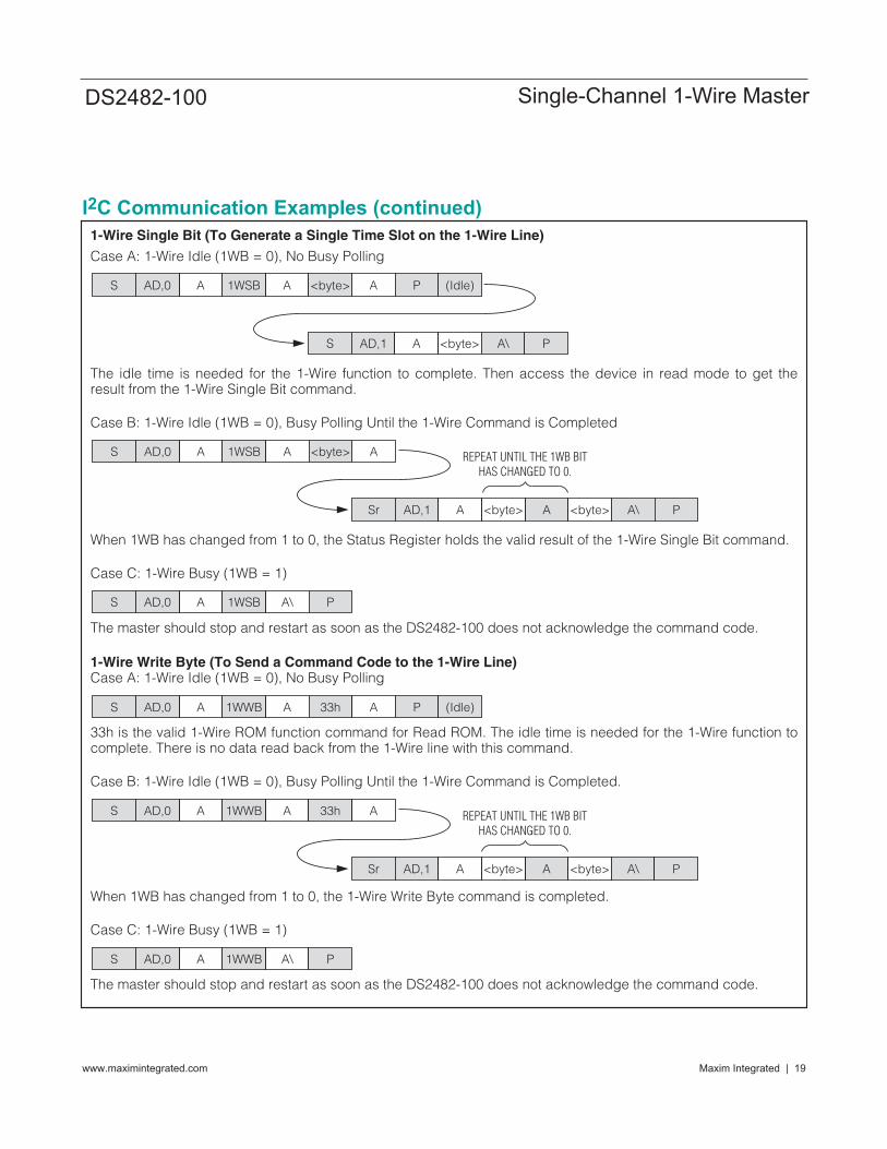
1-Wire Single Bit (To Generate a Single Time Slot on the 1-Wire Line)
Case A: 1-Wire Idle (1WB = 0), No Busy Polling
The idle time is needed for the 1-Wire function to complete. Then access the device in read mode to get theresult from the 1-Wire Single Bit command.
Case B: 1-Wire Idle (1WB = 0), Busy Polling Until the 1-Wire Command is Completed
When 1WB has changed from 1 to 0, the Status Register holds the valid result of the 1-Wire Single Bit command.
Case C: 1-Wire Busy (1WB = 1)
The master should stop and restart as soon as the DS2482-100 does not acknowledge the command code.
1-Wire Write Byte (To Send a Command Code to the 1-Wire Line)Case A: 1-Wire Idle (1WB = 0), No Busy Polling
33h is the valid 1-Wire ROM function command for Read ROM. The idle time is needed for the 1-Wire function tocomplete. There is no data read back from the 1-Wire line with this command.
Case B: 1-Wire Idle (1WB = 0), Busy Polling Until the 1-Wire Command is Completed.
When 1WB has changed from 1 to 0, the 1-Wire Write Byte command is completed.
Case C: 1-Wire Busy (1WB = 1)
The master should stop and restart as soon as the DS2482-100 does not acknowledge the command code.
S AD,0 A 1WWB A\ P
S AD,0 A 1WWB A 33h A
AD,1Sr A A<byte> <byte> A\ P
REPEAT UNTIL THE 1WB BITHAS CHANGED TO 0.
S AD,0 A 1WWB A 33h A P (Idle)
S AD,0 A 1WSB A\ P
S AD,0 A 1WSB A A<byte>
Sr AD,1 A A<byte> <byte> A\ P
REPEAT UNTIL THE 1WB BITHAS CHANGED TO 0.
S AD,0 A 1WSB A A<byte> P (Idle)
S AD,1 A <byte> A\ P
I2C Communication Examples (continued)
Maxim Integrated | 20www.maximintegrated.com
DS2482-100 Single-Channel 1-Wire Master
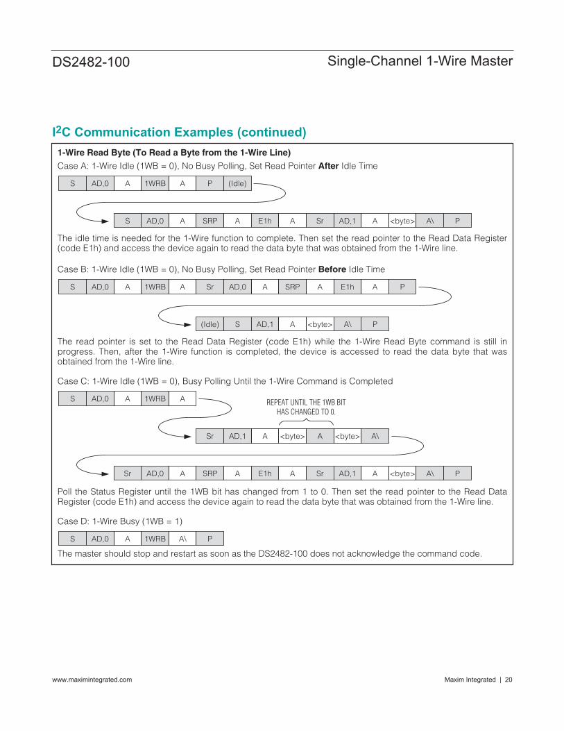
1-Wire Read Byte (To Read a Byte from the 1-Wire Line)
Case A: 1-Wire Idle (1WB = 0), No Busy Polling, Set Read Pointer After Idle Time
The idle time is needed for the 1-Wire function to complete. Then set the read pointer to the Read Data Register(code E1h) and access the device again to read the data byte that was obtained from the 1-Wire line.
Case B: 1-Wire Idle (1WB = 0), No Busy Polling, Set Read Pointer Before Idle Time
The read pointer is set to the Read Data Register (code E1h) while the 1-Wire Read Byte command is still inprogress. Then, after the 1-Wire function is completed, the device is accessed to read the data byte that wasobtained from the 1-Wire line.
Case C: 1-Wire Idle (1WB = 0), Busy Polling Until the 1-Wire Command is Completed
Poll the Status Register until the 1WB bit has changed from 1 to 0. Then set the read pointer to the Read DataRegister (code E1h) and access the device again to read the data byte that was obtained from the 1-Wire line.
Case D: 1-Wire Busy (1WB = 1)
The master should stop and restart as soon as the DS2482-100 does not acknowledge the command code.
S AD,0 A 1WRB A\ P
S AD,0 A 1WRB
AD,0 A SRP
A
A E1h A
Sr AD,1 A <byte> A
Sr AD,1 A <byte> A\ P
<byte> A\
REPEAT UNTIL THE 1WB BITHAS CHANGED TO 0.
Sr
S AD,0 A 1WRB A Sr AD,0 A SRP E1h A PA
(Idle) S AD,1 A <byte> PA\
S AD,0 A 1WRB A P (Idle)
S AD,0 A SRP AD,1 A <byte>A E1h A Sr PA\
I2C Communication Examples (continued)
Maxim Integrated | 21www.maximintegrated.com
DS2482-100 Single-Channel 1-Wire Master
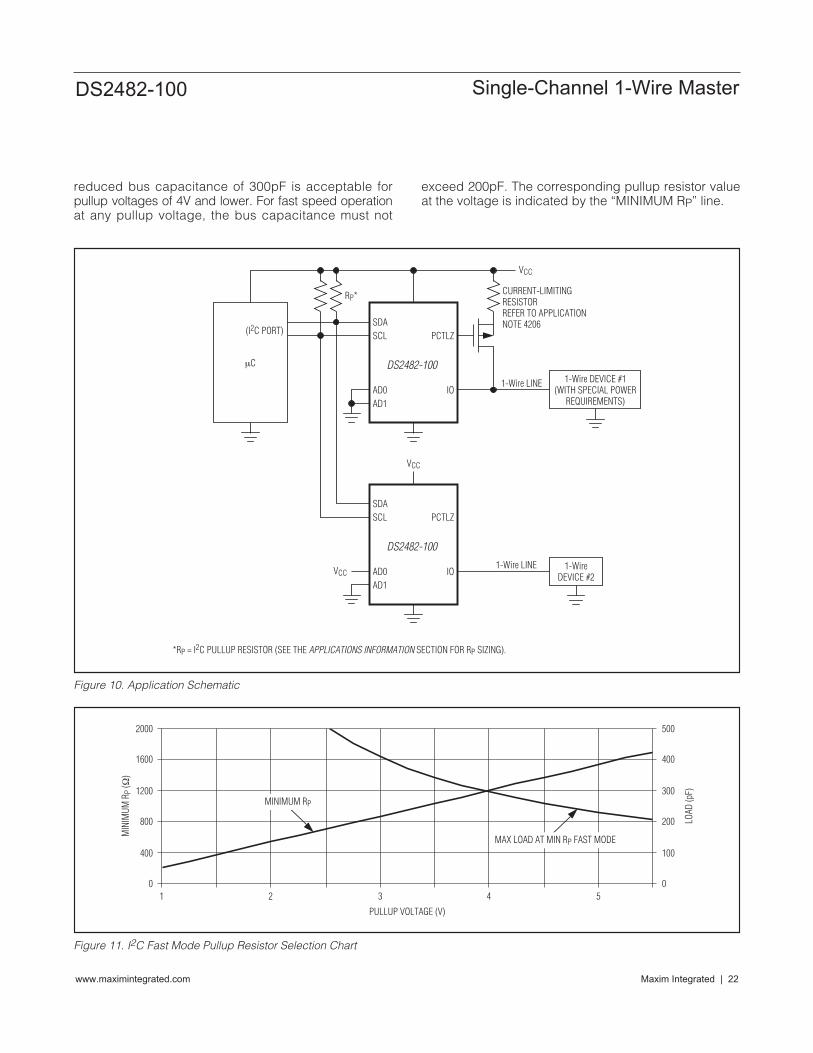
Applications Information
SDA and SCL Pullup ResistorsSDA is an open-drain output on the DS2482-100 thatrequires a pullup resistor to realize high-logic levels.Because the DS2482-100 uses SCL only as input (noclock stretching), the master can drive SCL eitherthrough an open-drain/-collector output with a pullupresistor or a push-pull output.
Pullup Resistor RP SizingAccording to the I2C specification, a slave device mustbe able to sink at least 3mA at a VOL of 0.4V. This DCcondition determines the minimum value of the pullupresistor as:
RP(MIN) = (VCC - 0.4V)/3mA
With an operating voltage of 5.5V, the minimum valuefor the pullup resistor is 1.7kΩ. The “MINIMUM RP” linein Figure 11 shows how the minimum pullup resistorchanges with the operating voltage.
For I2C systems, the rise time and fall time are mea-sured from 30% to 70% of the pullup voltage. The maxi-mum bus capacitance, CB, is 400pF. The maximum rise
time must not exceed 1000ns at standard speed and300ns at fast speed. Assuming maximum rise time, themaximum resistor value at any given capacitance CB iscalculated as:
RPMAXS = 1000ns/[CB x ln(7/3)] (standard speed)
RPMAXF = 300ns/[CB x ln(7/3)] (fast speed)
For a bus capacitance of 400pF, the maximum pullupresistor values are 2.95kΩ at standard speed and 885Ωat fast speed. A value between 1.7kΩ and 2.95kΩmeets all requirements at standard speed.
Because an 885Ω pullup resistor, as would be requiredto meet the rise time specification at fast speed and400pF bus capacitance, is lower than RP(MIN) at 5.5V, adifferent approach is necessary. The “MAX LOAD ATMIN RP FAST MODE” line in Figure 11 is generated byfirst calculating the minimum pullup resistor at anygiven operating voltage (“MINIMUM RP” line) and thencalculating the respective bus capacitance that yields a300ns rise time.
Only for pullup voltages of 3V and lower can the maximumpermissible bus capacitance of 400pF be maintained. A
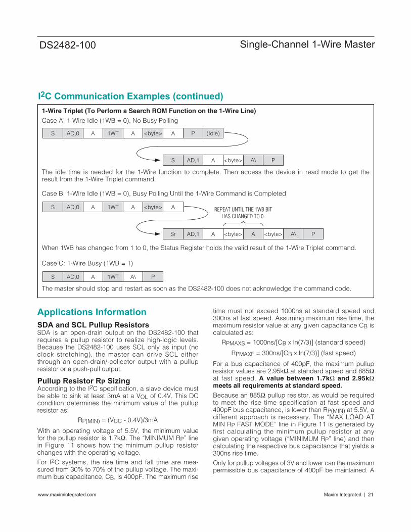
1-Wire Triplet (To Perform a Search ROM Function on the 1-Wire Line)
Case A: 1-Wire Idle (1WB = 0), No Busy Polling
The idle time is needed for the 1-Wire function to complete. Then access the device in read mode to get theresult from the 1-Wire Triplet command.
Case B: 1-Wire Idle (1WB = 0), Busy Polling Until the 1-Wire Command is Completed
When 1WB has changed from 1 to 0, the Status Register holds the valid result of the 1-Wire Triplet command.
Case C: 1-Wire Busy (1WB = 1)
The master should stop and restart as soon as the DS2482-100 does not acknowledge the command code.
S AD,0 A 1WT A\ P
S AD,0 A 1WT A <byte> A
Sr AD,1 A <byte> A <byte> A\ P
REPEAT UNTIL THE 1WB BITHAS CHANGED TO 0.
S AD,0 A 1WT A <byte> A P (Idle)
S AD,1 A <byte> A\ P
I2C Communication Examples (continued)
Maxim Integrated | 22www.maximintegrated.com
DS2482-100 Single-Channel 1-Wire Master
DS2482-100
SDASCL
AD1AD0
PCTLZ
IO
RP*
*RP = I2C PULLUP RESISTOR (SEE THE APPLICATIONS INFORMATION SECTION FOR RP SIZING).
VCC
VCC
VCC
CURRENT-LIMITINGRESISTORREFER TO APPLICATIONNOTE 4206
1-Wire LINE
1-Wire LINE
1-Wire DEVICE #1(WITH SPECIAL POWER
REQUIREMENTS)
1-WireDEVICE #2
DS2482-100
SDASCL
AD0AD1
PCTLZ
IO
μC
(I2C PORT)
Figure 10. Application Schematic
MINIMUM RP
MAX LOAD AT MIN RP FAST MODE
2000
MIN
IMUM
RP
(Ω)
LOAD
(pF)
PULLUP VOLTAGE (V)
1600
1200
800
400
1 2 3 4 50
500
400
300
200
100
0
Figure 11. I2C Fast Mode Pullup Resistor Selection Chart
reduced bus capacitance of 300pF is acceptable forpullup voltages of 4V and lower. For fast speed operationat any pullup voltage, the bus capacitance must not
exceed 200pF. The corresponding pullup resistor valueat the voltage is indicated by the “MINIMUM RP” line.
Maxim Integrated | 23www.maximintegrated.com
DS2482-100 Single-Channel 1-Wire Master
PCTLZ
SDASCL
1
2
8
7
AD0
AD1IO
GND
VCC
SO (150 mils)
TOP VIEW
3
4
6
5
DS2482-100
WLP
TOP VIEW(BUMP SIDE DOWN)
1 2 3
B
C
A
PCTLZ AD1 AD0
SCL SDA VCC
GND IO
+
DS2482-100 DS2482-100
WLP
1 2 3
B
C
A
+
TOP MARK
2 4 8 2 1
y y w w r r
# # # x x
+
Pin Configurations
Package InformationFor the latest package outline information and land patterns (footprints), go to www.maxim-integrated.com/packages. Note that a“+”, “#”, or “-” in the package code indicates RoHS status only. Package drawings may show a different suffix character, but the draw-ing pertains to the package regardless of RoHS status.
PACKAGE TYPE PACKAGE CODE OUTLINE NO. LAND PATTERN NO.
8 SO (150 mils) S8+4 21-0041 90-0096
9 WLP W92A1+1 21-0067Refer to
Application Note 1891
Ordering Information
+Denotes a lead(Pb)-free/RoHS-compliant package.T/T&R = Tape and reel.
PART TEMP RANGE PIN-PACKAGE
DS2482S-100+ -40°C to +85°C 8 SO (150 mils)
DS2482S-100+T&R -40°C to +85°C 8 SO (150 mils)
DS2482X-100+T -40°C to +85°C 9 WLP (2.5k pieces)
Maxim Integrated cannot assume responsibility for use of any circuitry other than circuitry entirely embodied in a Maxim Integrated product. No circuit patentlicenses are implied. Maxim Integrated reserves the right to change the circuitry and specifications without notice at any time. The parametric values (min andmax limits) shown in the Electrical Characteristics table are guaranteed. Other parametric values quoted in this data sheet are provided for guidance.
Maxim Integrated and the Maxim Integrated logo are trademarks of Maxim Integrated Products, Inc. © 2015 Maxim Integrated Products, Inc. | 24
For pricing, delivery, and ordering information, please contact Maxim Direct at 1-888-629-4642, or visit Maxim Integrated’s website at www.maximintegrated.com.
DS2482-100 Single-Channel 1-Wire Master
Revision History
REVISION NUMBER
REVISION DATE
DESCRIPTION PAGES
CHANGED
1 080604 Initial release —
2 110204I2C trademark note deleted; upper I2C slave address bits changed from 01100b to 00110b.
1, 14
3 040507 Added the lead(Pb)-free ordering information. 1
4 091007 Added the UCSP (WLP) package and Package Information section. 1, 21
Updated the Features bullets. 1
Updated the VIL1 and RWPU values in the Electrical Characteristics table. 2
Minor corrections to Figure 1; updated the Detailed Description section to clarify information about the active pullup and strong pullup.
5
Replaced the Strong Pullup (SPU) section description and replaced Figure 4. 7
5 061208
Removed timing inaccuracies in Figure 8. 14
Created newer template-style data sheet. All 6 7/08
Replaced Figure 8. 16
7 8/08Deleted the 1-Wire line termination resistor and references to it in the Typical Operating Circuit and in Figure 11.
1, 23
8 11/09Corrected the recommendation for using active pullup (APU); removed the references to presence-pulse masking.
1–7, 9–12, 15, 16, 21, 22, 24
9 1/12
Updated the soldering information in the Absolute Maximum Ratings section; added a note to the Strong Pullup (SPU) section description; updated the 1-Wire Reset command description (sections Restriction and Configuration Bits Affected); added the land pattern to the Package Information section.
2, 7, 10, 23
10 1/15 Updated Benefits and Features section 1