Embed Size (px)
Citation preview
100Q STP Cable
FP
D-L
ink
Dis
play
Inte
rfac
e
RGB Display720p
24-bit Color Depth
DS90UB927Q-Q1Serializer
DS90UB928Q-Q1Deserializer
FPD-Link III 1 Pair/AC Coupled
VDDIO (1.8V or 3.3V)
FPD-LinkFPD-Link
RxIN1+/-
RxCLKIN+/-
RxIN2+/-
RxIN0+/-
RxIN3+/-
TxOUT1+/-
TxCLKOUT+/-
TxOUT2+/-
TxOUT0+/-
TxOUT3+/-
VDDIO (1.8V or 3.3V)
HOSTGraphics
Processor
DOUT+
DOUT-
RIN+
RIN-
SDASCL
I2SMCLK
66
VDD33 (3.3V)
VDD33 (3.3V)
MODE_SELBISTEN
LFMODEMAPSEL
PDBOSS_SEL
OEN
BKWDREPEATLFMODEMAPSEL
IDxSDASCL
LOCKPASS
PDBINTBI2S
INTB_IN
IDx
Product
Folder
Sample &Buy
Technical
Documents
Tools &
Software
Support &Community
DS90UB927Q-Q1SNLS416D –JUNE 2012–REVISED JANUARY 2015
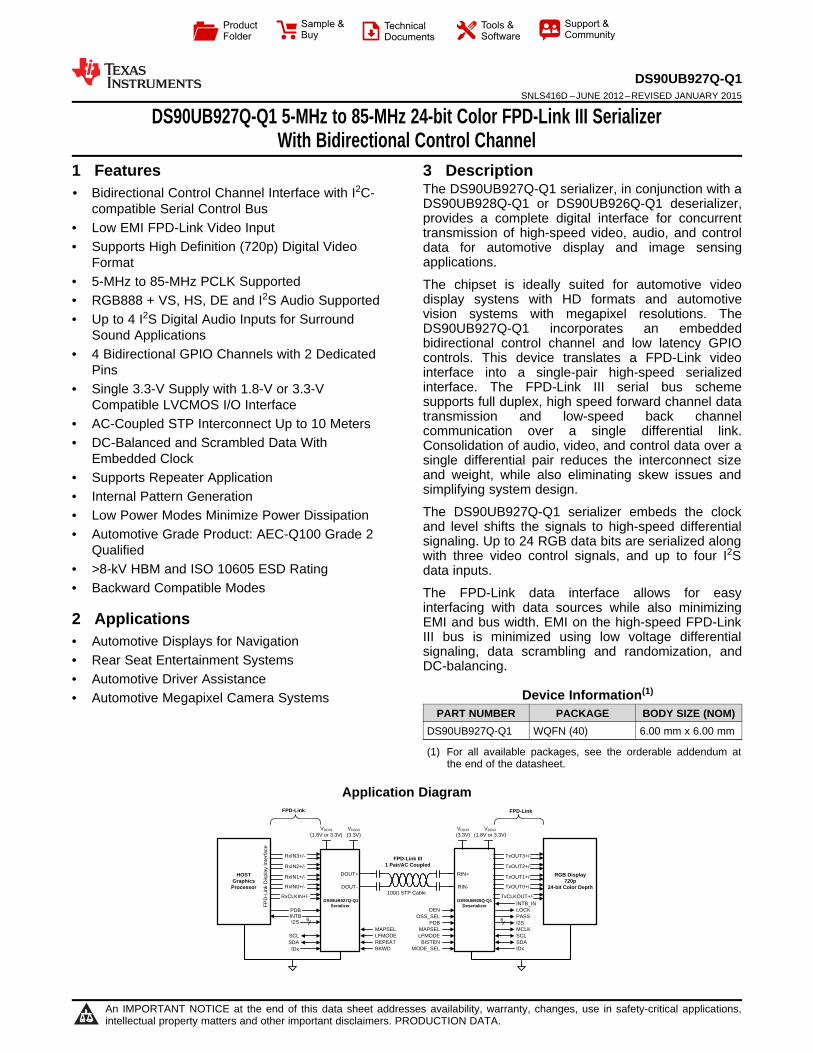
DS90UB927Q-Q1 5-MHz to 85-MHz 24-bit Color FPD-Link III SerializerWith Bidirectional Control Channel
1 Features 3 DescriptionThe DS90UB927Q-Q1 serializer, in conjunction with a
1• Bidirectional Control Channel Interface with I2C-DS90UB928Q-Q1 or DS90UB926Q-Q1 deserializer,compatible Serial Control Busprovides a complete digital interface for concurrent
• Low EMI FPD-Link Video Input transmission of high-speed video, audio, and control• Supports High Definition (720p) Digital Video data for automotive display and image sensing
applications.Format• 5-MHz to 85-MHz PCLK Supported The chipset is ideally suited for automotive video
display systens with HD formats and automotive• RGB888 + VS, HS, DE and I2S Audio Supportedvision systems with megapixel resolutions. The• Up to 4 I2S Digital Audio Inputs for SurroundDS90UB927Q-Q1 incorporates an embeddedSound Applications bidirectional control channel and low latency GPIO
• 4 Bidirectional GPIO Channels with 2 Dedicated controls. This device translates a FPD-Link videoPins interface into a single-pair high-speed serialized
interface. The FPD-Link III serial bus scheme• Single 3.3-V Supply with 1.8-V or 3.3-Vsupports full duplex, high speed forward channel dataCompatible LVCMOS I/O Interfacetransmission and low-speed back channel• AC-Coupled STP Interconnect Up to 10 Meters communication over a single differential link.
• DC-Balanced and Scrambled Data With Consolidation of audio, video, and control data over aEmbedded Clock single differential pair reduces the interconnect size
and weight, while also eliminating skew issues and• Supports Repeater Applicationsimplifying system design.• Internal Pattern GenerationThe DS90UB927Q-Q1 serializer embeds the clock• Low Power Modes Minimize Power Dissipationand level shifts the signals to high-speed differential• Automotive Grade Product: AEC-Q100 Grade 2 signaling. Up to 24 RGB data bits are serialized along
Qualified with three video control signals, and up to four I2S• >8-kV HBM and ISO 10605 ESD Rating data inputs.• Backward Compatible Modes The FPD-Link data interface allows for easy
interfacing with data sources while also minimizing2 Applications EMI and bus width. EMI on the high-speed FPD-Link
III bus is minimized using low voltage differential• Automotive Displays for Navigationsignaling, data scrambling and randomization, and• Rear Seat Entertainment Systems DC-balancing.
• Automotive Driver AssistanceDevice Information(1)• Automotive Megapixel Camera Systems
PART NUMBER PACKAGE BODY SIZE (NOM)DS90UB927Q-Q1 WQFN (40) 6.00 mm x 6.00 mm
(1) For all available packages, see the orderable addendum atthe end of the datasheet.
Application Diagram
1
An IMPORTANT NOTICE at the end of this data sheet addresses availability, warranty, changes, use in safety-critical applications,intellectual property matters and other important disclaimers. PRODUCTION DATA.
DS90UB927Q-Q1SNLS416D –JUNE 2012–REVISED JANUARY 2015 www.ti.com
Table of Contents7.2 Functional Block Diagram ....................................... 151 Features .................................................................. 17.3 Feature Description................................................. 162 Applications ........................................................... 17.4 Device Functional Modes........................................ 233 Description ............................................................. 17.5 Programming........................................................... 294 Revision History..................................................... 27.6 Register Maps ......................................................... 315 Pin Configuration and Functions ......................... 3
8 Application and Implementation ........................ 446 Specifications......................................................... 58.1 Application Information............................................ 446.1 Absolute Maximum Ratings ...................................... 58.2 Typical Application .................................................. 446.2 ESD Ratings.............................................................. 58.3 System Examples ................................................... 466.3 Recommended Operating Conditions....................... 6
9 Power Supply Recommendations ...................... 486.4 Thermal Information .................................................. 610 Layout................................................................... 486.5 DC Electrical Characteristics .................................... 7
10.1 Layout Guidelines ................................................. 486.6 AC Electrical Characteristics..................................... 910.2 Layout Example .................................................... 496.7 Electrical Characteristics: DC and AC Serial Control
Bus ........................................................................... 10 11 Device and Documentation Support ................. 516.8 Timing Requirements for the Serial Control Bus .... 11 11.1 Documentation Support ........................................ 516.9 Timing Requirements - DC and AC Serial Control 11.2 Trademarks ........................................................... 51
Bus Characteristics .................................................. 11 11.3 Electrostatic Discharge Caution............................ 516.10 Typical Characteristics .......................................... 14 11.4 Glossary ................................................................ 51
7 Detailed Description ............................................ 15 12 Mechanical, Packaging, and Orderable7.1 Overview ................................................................. 15 Information ........................................................... 51
4 Revision HistoryNOTE: Page numbers for previous revisions may differ from page numbers in the current version.
Changes from Revision C (October 2012) to Revision D Page
• Added ESD Ratings table, Feature Description section, Device Functional Modes, Application and Implementationsection, Power Supply Recommendations section, Layout section, Device and Documentation Support section, andMechanical, Packaging, and Orderable Information section .................................................................................................. 1
Changes from Revision B (June 2012) to Revision C Page
• Changed layout of National data sheet to tI format.............................................................................................................. 49
2 Submit Documentation Feedback Copyright © 2012–2015, Texas Instruments Incorporated
Product Folder Links: DS90UB927Q-Q1
11
12
13
14
15
16
17
18
19
20
40
39
38
37
36
35
34
33
32
31
1 2 3 4 5 6 7 8 9
RxIN1-
RxIN1+
RxIN2-
RxIN2+
RxCLKIN-
GPIO1
RxIN3-
RxIN3+
GPIO0
RES1
CAPHS12
RES0
IDx
CAPP12
DOUT-
CMF
VDD33_A
PDB
DOUT+
RE
PE
AT
BK
WD
MA
PS
EL
LFM
OD
E
VD
D33
_B
I2S
_WC
/GP
IO_R
EG
7
CA
PLV
D12
RxI
N0-
RxI
N0+
SD
A
SC
L
CA
PL1
2
VD
DIO
I2S
_DC
/GP
I02
I2S
_DD
/GP
I03
I2S
_DB
/GP
IO_R
EG
5
I2S
_DA
/GP
IO_R
EG
6
I2S
_CLK
/GP
IO_R
EG
8
INT
BRxCLKIN+
VD
DIO
30 29 28 27 26 25 24 23 22 21
DS90UB927Q-Q1
DAP = GND
10
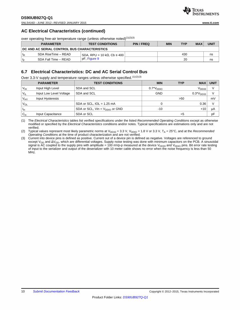
DS90UB927Q-Q1www.ti.com SNLS416D –JUNE 2012–REVISED JANUARY 2015
5 Pin Configuration and Functions
RTA Package40-Pin WQFN With Exposed Thermal Pad
Top View
Pin FunctionsPIN
I/O DESCRIPTIONNAME NO.FPD-LINK INPUT INTERFACE
Inverting LVDS Clock InputRxCLKIN- 35 I, LVDS The pair requires external 100-Ω differential termination for standard LVDS levelsTrue LVDS Clock InputRxCLKIN+ 36 I, LVDS The pair requires external 100-Ω differential termination for standard LVDS levels
37, 33, Inverting LVDS Data InputsRxIN[3:0]- I, LVDS31, 29 Each pair requires external 100-Ω differential termination for standard LVDS levels38, 34, True LVDS Data InputsRxIN[3:0]+ I, LVDS32, 30 Each pair requires external 100-Ω differential termination for standard LVDS levels
LVCMOS PARALLEL INTERFACEBackward Compatible Mode Select
I, LVCMOS BKWD = 0, interfacing to DS90UH926/8Q-Q1 (Default)BKWD 22 with pulldown BKWD = 1, interfacing to DS90UR906/8Q-Q1, DS90UR916QRequires a 10-kΩ pullup if set HIGH
I/O, LVCMOS General Purpose I/OGPIO[1:0] 40, 39 with pulldown See Table 1I2S_DA 3I2S_DB 4 I, LVCMOS Digital Audio Interface I2S Data InputsI2S_DC 5 with pulldown Shared with GPIO_REG6, GPIO_REG5, GPIO2, GPIO3I2S_DD 6I2S_WC 1 I, LVCMOS Digital Audio Interface I2S Word Clock and I2S Bit Clock InputsI2S_CLK 2 with pulldown Shared with GPIO_REG7 and GPIO_REG8 (Table 3)
Copyright © 2012–2015, Texas Instruments Incorporated Submit Documentation Feedback 3
Product Folder Links: DS90UB927Q-Q1
DS90UB927Q-Q1SNLS416D –JUNE 2012–REVISED JANUARY 2015 www.ti.com
Pin Functions (continued)PIN
I/O DESCRIPTIONNAME NO.
Low Frequency Mode SelectI, LVCMOS LFMODE = 0, 15 MHz ≤ RxCLKIN ≤ 85 MHz (Default)LFMODE 25 with pulldown LFMODE = 1, 5 MHz ≤ RxCLKIN < 15 MHz
Requires a 10-kΩ pullup if set HIGHFPD-Link Input Map SelectMAPSEL = 0, LSBs on RxIN3± (Default)I, LVCMOSMAPSEL 23 MAPSEL = 1, MSBs on RxIN3±with pulldown See Figure 19 and Figure 20Requires a 10-kΩ pullup if set HIGHRepeater Mode Select
I, LVCMOS REPEAT = 0, Repeater Mode disabled (Default)REPEAT 21 with pulldown REPEAT = 1, Repeater Mode enabledRequires a 10-kΩ pullup if set HIGH
OPTIONAL PARALLEL INTERFACEI/O, LVCMOS General Purpose I/OGPIO[3:2] 6, 5 with pulldown Shared with I2S_DD and I2S_DC (See Table 1)
GPIO_REG I/O, LVCMOS Register-Only General Purpose I/O2, 1, 3, 4[8:5] with pulldown Shared with I2S_CLK, I2S_WC, I2S_DA, I2S_DB (See Table 2)CONTROL AND CONFIGURATION
I2C Address SelectExternal pullup to VDD33 is required under all conditions. DO NOT FLOAT.IDx 11 I, Analog Connect to external pullup to VDD33 and pulldown to GND to create a voltage divider.See Figure 25 and Table 4Power-down Mode Input PinMust be driven or pulled up to VDD33. Refer to Power Supply Recommendations.
I, LVCMOS PDB = H, device is enabled (normal operation)PDB 18 with pulldown PDB = L, device is powered down.When the device is in the powered down state, the Driver Outputs are both HIGH, the PLL isshutdown, and IDD is minimized. Control Registers are RESET.I2C Clock Input / Output InterfaceI/O, LVCMOSSCL 9 Must have an external pullup to VDD33. DO NOT FLOAT.Open Drain Recommended pullup: 4.7 kΩ.I2C Data Input / Output InterfaceI/O, LVCMOSSDA 10 Must have an external pullup to VDD33. DO NOT FLOAT.Open Drain Recommended pullup: 4.7 kΩ.
STATUSInterrupt
O, LVCMOS INTB = H, normalINTB 27 Open Drain INTB = L, Interrupt requestRecommended pullup: 4.7 kΩ to VDDIO. DO NOT FLOAT.
FPD-LINK III SERIAL INTERFACECommon Mode Filter.CMF 20 Analog Connect 0.1 µF to GND (required)Inverting OutputDOUT- 16 I/O, LVDS The output must be AC-coupled with a 0.1-µF capacitor.True OutputDOUT+ 17 I/O, LVDS The output must be AC-coupled with a 0.1-µF capacitor.
4 Submit Documentation Feedback Copyright © 2012–2015, Texas Instruments Incorporated
Product Folder Links: DS90UB927Q-Q1
DS90UB927Q-Q1www.ti.com SNLS416D –JUNE 2012–REVISED JANUARY 2015
Pin Functions (continued)PIN
I/O DESCRIPTIONNAME NO.POWER (1) AND GROUND
Large metal contact at the bottom center of the device package Connect to the groundGND DAP Ground plane (GND) with at least 9 vias.VDD33_A 19 Power Power to on-chip regulator 3.0 V - 3.6 V. Each pin requires a 4.7-µF capacitor to GNDVDD33_B 26VDDIO 7, 24 Power LVCMOS I/O Power 1.8 V ±5% OR 3.0 V - 3.6 V. Each pin requires 4.7-µF capacitor to GNDREGULATOR CAPACITOR
Decoupling capacitor connection for on-chip regulatorCAPL12 8 CAP Requires two 4.7-µF decoupling capacitors to GNDCAPP12 12 Decoupling capacitor connection for on-chip regulatorCAPHS12 14 CAP Each requires a 4.7-µF decoupling capacitor to GND.CAPLVD12 28OTHER
ReservedRES[1:0] 15, 13 GND Connect to GND.
(1) The VDD (VDD33 and VDDIO) supply ramp should be faster than 1.5 ms with a monotonic rise.
6 Specifications
6.1 Absolute Maximum Ratings (1) (2) (3)
MIN MAX UNITSupply Voltage – VDD33 −0.3 4.0 VSupply Voltage – VDDIO −0.3 4.0 VLVCMOS I/O Voltage −0.3 VDDIO + 0.3 VSerializer Output Voltage −0.3 2.75 VJunction Temperature 150 °CStorage Temperature, Tstg −65 150 °C
(1) For soldering specifications: see product folder at www.ti.com and SNOA549.(2) Stresses beyond those listed under Absolute Maximum Ratings may cause permanent damage to the device. These are stress ratings
only, which do not imply functional operation of the device at these or any other conditions beyond those indicated under RecommendedOperating Conditions. Exposure to absolute-maximum-rated conditions for extended periods may affect device reliability.
(3) If Military/Aerospace specified devices are required, please contact the Texas Instruments Sales Office/Distributors for availability andspecifications.
6.2 ESD RatingsVALUE UNIT
Human body model (HBM), per AEC Q100-002 (1) ±8000Charged device model (CDM), per AEC Q100-011 ±1250Machine model (MM) ±250(IEC 61000-4-2, powered-up only) Air Discharge ±15000RD = 330 Ω, CS = 150 pF (Pin 16 and 17)ElectrostaticV(ESD) VContact Dischargedischarge ±8000(Pin 16 and 17)(ISO 10605) Air Discharge ±15000RD = 330 Ω, CS = 150 pF/330 pF (Pin 16 and 17)RD = 2 kΩ, CS = 150 pF/330 pF Contact Discharge ±8000(Pin 16 and 17)
(1) AEC Q100-002 indicates HBM stressing is done in accordance with the ANSI/ESDA/JEDEC JS-001 specification.
Copyright © 2012–2015, Texas Instruments Incorporated Submit Documentation Feedback 5
Product Folder Links: DS90UB927Q-Q1
DS90UB927Q-Q1SNLS416D –JUNE 2012–REVISED JANUARY 2015 www.ti.com
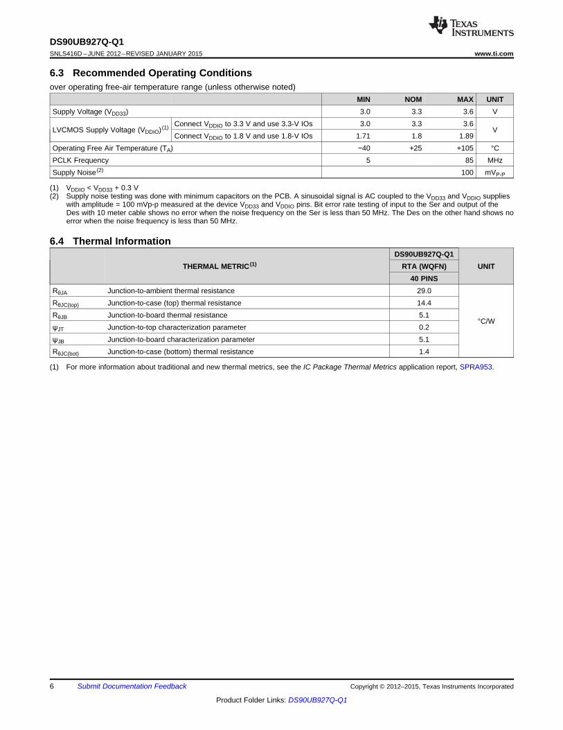
6.3 Recommended Operating Conditionsover operating free-air temperature range (unless otherwise noted)
MIN NOM MAX UNITSupply Voltage (VDD33) 3.0 3.3 3.6 V
Connect VDDIO to 3.3 V and use 3.3-V IOs 3.0 3.3 3.6LVCMOS Supply Voltage (VDDIO) (1) V
Connect VDDIO to 1.8 V and use 1.8-V IOs 1.71 1.8 1.89Operating Free Air Temperature (TA) −40 +25 +105 °CPCLK Frequency 5 85 MHzSupply Noise (2) 100 mVP-P
(1) VDDIO < VDD33 + 0.3 V(2) Supply noise testing was done with minimum capacitors on the PCB. A sinusoidal signal is AC coupled to the VDD33 and VDDIO supplies
with amplitude = 100 mVp-p measured at the device VDD33 and VDDIO pins. Bit error rate testing of input to the Ser and output of theDes with 10 meter cable shows no error when the noise frequency on the Ser is less than 50 MHz. The Des on the other hand shows noerror when the noise frequency is less than 50 MHz.
6.4 Thermal InformationDS90UB927Q-Q1
THERMAL METRIC (1) RTA (WQFN) UNIT40 PINS
RθJA Junction-to-ambient thermal resistance 29.0RθJC(top) Junction-to-case (top) thermal resistance 14.4RθJB Junction-to-board thermal resistance 5.1
°C/WψJT Junction-to-top characterization parameter 0.2ψJB Junction-to-board characterization parameter 5.1RθJC(bot) Junction-to-case (bottom) thermal resistance 1.4
(1) For more information about traditional and new thermal metrics, see the IC Package Thermal Metrics application report, SPRA953.
6 Submit Documentation Feedback Copyright © 2012–2015, Texas Instruments Incorporated
Product Folder Links: DS90UB927Q-Q1
DS90UB927Q-Q1www.ti.com SNLS416D –JUNE 2012–REVISED JANUARY 2015
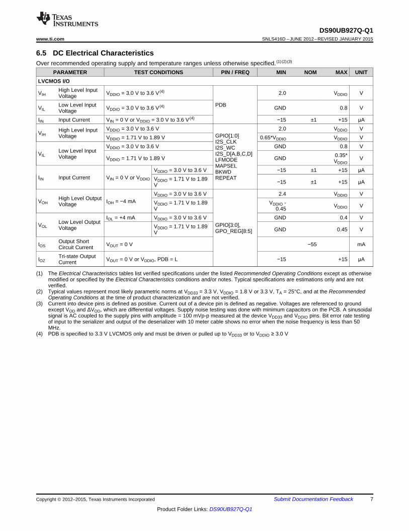
6.5 DC Electrical CharacteristicsOver recommended operating supply and temperature ranges unless otherwise specified. (1) (2) (3)
PARAMETER TEST CONDITIONS PIN / FREQ MIN NOM MAX UNITLVCMOS I/O
High Level InputVIH VDDIO = 3.0 V to 3.6 V (4) 2.0 VDDIO VVoltageLow Level Input PDBVIL VDDIO = 3.0 V to 3.6 V (4) GND 0.8 VVoltage
IIN Input Current VIN = 0 V or VDDIO = 3.0 V to 3.6 V (4) −15 ±1 +15 μAVDDIO = 3.0 V to 3.6 V 2.0 VDDIO VHigh Level InputVIH GPIO[1:0]Voltage VDDIO = 1.71 V to 1.89 V 0.65*VDDIO VDDIO V
I2S_CLKVDDIO = 3.0 V to 3.6 V GND 0.8 VI2S_WCLow Level InputVIL I2S_D[A,B,C,D] 0.35*Voltage VDDIO = 1.71 V to 1.89 V GND VLFMODE VDDIOMAPSEL
VDDIO = 3.0 V to 3.6 V −15 ±1 +15 μABKWDIIN Input Current VIN = 0 V or VDDIO REPEATVDDIO = 1.71 V to 1.89 −15 ±1 +15 μAV
VDDIO = 3.0 V to 3.6 V 2.4 VDDIO VHigh Level OutputVOH IOH = −4 mA VDDIO = 1.71 V to 1.89 VDDIO -Voltage VDDIO VV 0.45
IOL = +4 mA VDDIO = 3.0 V to 3.6 V GND 0.4 VLow Level OutputVOL GPIO[3:0],VDDIO = 1.71 V to 1.89Voltage GND 0.45 VGPO_REG[8:5]VOutput ShortIOS VOUT = 0 V −55 mACircuit CurrentTri-state OutputIOZ VOUT = 0 V or VDDIO, PDB = L −15 +15 μACurrent
(1) The Electrical Characteristics tables list verified specifications under the listed Recommended Operating Conditions except as otherwisemodified or specified by the Electrical Characteristics conditions and/or notes. Typical specifications are estimations only and are notverified.
(2) Typical values represent most likely parametric norms at VDD33 = 3.3 V, VDDIO = 1.8 V or 3.3 V, TA = 25°C, and at the RecommendedOperating Conditions at the time of product characterization and are not verified.
(3) Current into device pins is defined as positive. Current out of a device pin is defined as negative. Voltages are referenced to groundexcept VOD and ΔVOD, which are differential voltages. Supply noise testing was done with minimum capacitors on the PCB. A sinusoidalsignal is AC coupled to the supply pins with amplitude = 100 mVp-p measured at the device VDD33 and VDDIO pins. Bit error rate testingof input to the serializer and output of the deserializer with 10 meter cable shows no error when the noise frequency is less than 50MHz.
(4) PDB is specified to 3.3 V LVCMOS only and must be driven or pulled up to VDD33 or to VDDIO ≥ 3.0 V
Copyright © 2012–2015, Texas Instruments Incorporated Submit Documentation Feedback 7
Product Folder Links: DS90UB927Q-Q1
DS90UB927Q-Q1SNLS416D –JUNE 2012–REVISED JANUARY 2015 www.ti.com
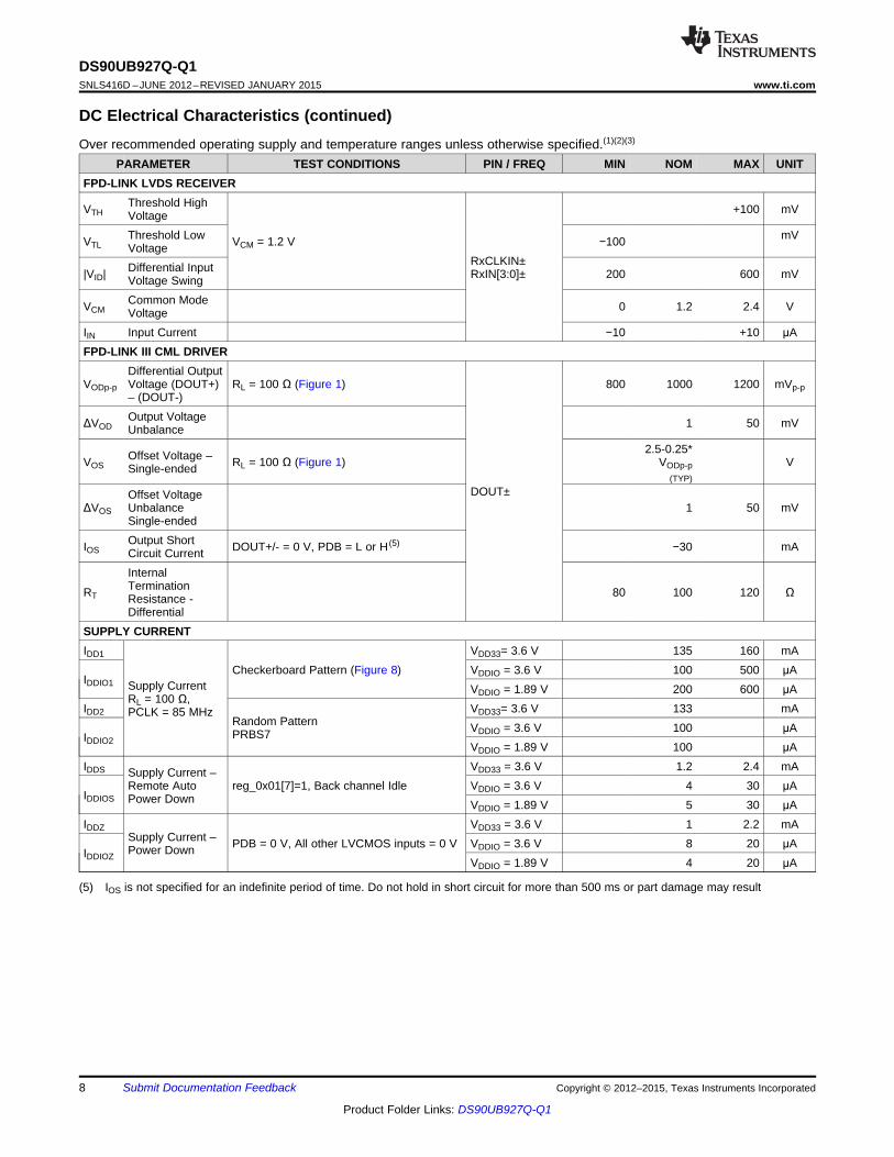
DC Electrical Characteristics (continued)Over recommended operating supply and temperature ranges unless otherwise specified.(1)(2)(3)
PARAMETER TEST CONDITIONS PIN / FREQ MIN NOM MAX UNITFPD-LINK LVDS RECEIVER
Threshold HighVTH +100 mVVoltageThreshold Low mVVTL VCM = 1.2 V −100Voltage
RxCLKIN±Differential Input|VID| RxIN[3:0]± 200 600 mVVoltage SwingCommon ModeVCM 0 1.2 2.4 VVoltage
IIN Input Current −10 +10 μAFPD-LINK III CML DRIVER
Differential OutputVODp-p Voltage (DOUT+) RL = 100 Ω (Figure 1) 800 1000 1200 mVp-p
– (DOUT-)Output VoltageΔVOD 1 50 mVUnbalance
2.5-0.25*Offset Voltage –VOS RL = 100 Ω (Figure 1) VODp-p VSingle-ended(TYP)
DOUT±Offset VoltageΔVOS Unbalance 1 50 mV
Single-endedOutput ShortIOS DOUT+/- = 0 V, PDB = L or H (5) −30 mACircuit CurrentInternalTerminationRT 80 100 120 ΩResistance -Differential
SUPPLY CURRENTIDD1 VDD33= 3.6 V 135 160 mA
Checkerboard Pattern (Figure 8) VDDIO = 3.6 V 100 500 μAIDDIO1 Supply Current VDDIO = 1.89 V 200 600 μA
RL = 100 Ω,IDD2 VDD33= 3.6 V 133 mAPCLK = 85 MHz
Random Pattern VDDIO = 3.6 V 100 μAPRBS7IDDIO2 VDDIO = 1.89 V 100 μAIDDS VDD33 = 3.6 V 1.2 2.4 mASupply Current –
Remote Auto reg_0x01[7]=1, Back channel Idle VDDIO = 3.6 V 4 30 μAIDDIOS Power Down VDDIO = 1.89 V 5 30 μAIDDZ VDD33 = 3.6 V 1 2.2 mA
Supply Current – PDB = 0 V, All other LVCMOS inputs = 0 V VDDIO = 3.6 V 8 20 μAPower DownIDDIOZ VDDIO = 1.89 V 4 20 μA
(5) IOS is not specified for an indefinite period of time. Do not hold in short circuit for more than 500 ms or part damage may result
8 Submit Documentation Feedback Copyright © 2012–2015, Texas Instruments Incorporated
Product Folder Links: DS90UB927Q-Q1
DS90UB927Q-Q1www.ti.com SNLS416D –JUNE 2012–REVISED JANUARY 2015
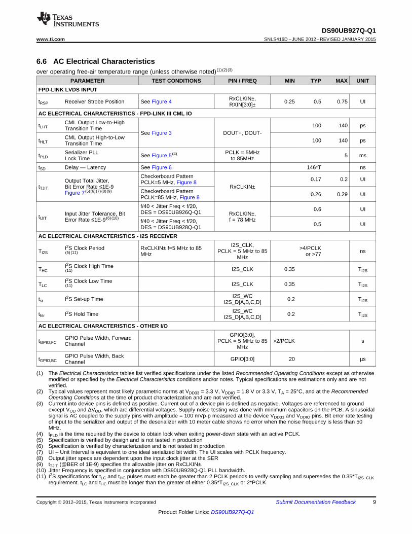
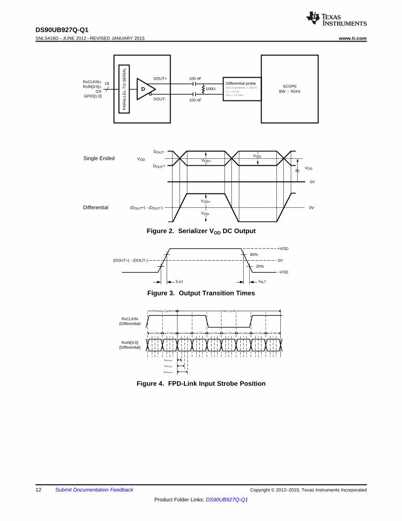
6.6 AC Electrical Characteristicsover operating free-air temperature range (unless otherwise noted) (1) (2) (3)
PARAMETER TEST CONDITIONS PIN / FREQ MIN TYP MAX UNITFPD-LINK LVDS INPUT
RxCLKIN±,tRSP Receiver Strobe Position See Figure 4 0.25 0.5 0.75 UIRXIN[3:0]±AC ELECTRICAL CHARACTERISTICS - FPD-LINK III CML IO
CML Output Low-to-HightLHT 100 140 psTransition TimeSee Figure 3 DOUT+, DOUT-
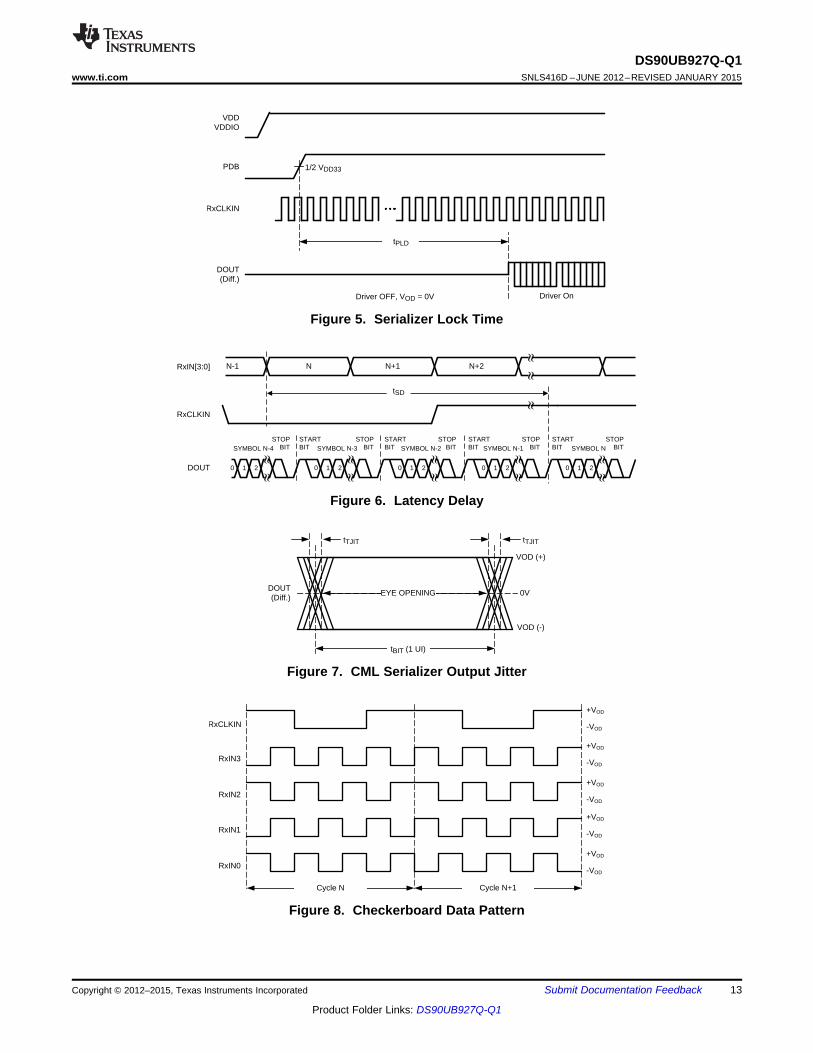
CML Output High-to-LowtHLT 100 140 psTransition TimeSerializer PLL PCLK = 5MHztPLD See Figure 5 (4) 5 msLock Time to 85MHz
tSD Delay — Latency See Figure 6 146*T nsCheckerboard Pattern 0.17 0.2 UIOutput Total Jitter, PCLK=5 MHz, Figure 8
tTJIT Bit Error Rate ≤1E-9 RxCLKIN±Checkerboard PatternFigure 7 (5) (6) (7) (8) (9) 0.26 0.29 UIPCLK=85 MHz, Figure 8f/40 < Jitter Freq < f/20, 0.6 UIDES = DS90UB926Q-Q1Input Jitter Tolerance, Bit RxCLKIN±,tIJIT Error Rate ≤1E-9 (6) (10) f = 78 MHzf/40 < Jitter Freq < f/20, 0.5 UIDES = DS90UB928Q-Q1
AC ELECTRICAL CHARACTERISTICS - I2S RECEIVERI2S_CLK,I2S Clock Period RxCLKIN± f=5 MHz to 85 >4/PCLKTI2S PCLK = 5 MHz to 85 ns(5) (11) MHz or >77MHz
I2S Clock High TimeTHC I2S_CLK 0.35 TI2S(11)
I2S Clock Low TimeTLC I2S_CLK 0.35 TI2S(11)
I2S_WCtsr I2S Set-up Time 0.2 TI2SI2S_D[A,B,C,D]I2S_WCthtr I2S Hold Time 0.2 TI2SI2S_D[A,B,C,D]
AC ELECTRICAL CHARACTERISTICS - OTHER I/OGPIO[3:0],GPIO Pulse Width, ForwardtGPIO,FC PCLK = 5 MHz to 85 >2/PCLK sChannel MHz
GPIO Pulse Width, BacktGPIO,BC GPIO[3:0] 20 µsChannel
(1) The Electrical Characteristics tables list verified specifications under the listed Recommended Operating Conditions except as otherwisemodified or specified by the Electrical Characteristics conditions and/or notes. Typical specifications are estimations only and are notverified.
(2) Typical values represent most likely parametric norms at VDD33 = 3.3 V, VDDIO = 1.8 V or 3.3 V, TA = 25°C, and at the RecommendedOperating Conditions at the time of product characterization and are not verified.
(3) Current into device pins is defined as positive. Current out of a device pin is defined as negative. Voltages are referenced to groundexcept VOD and ΔVOD, which are differential voltages. Supply noise testing was done with minimum capacitors on the PCB. A sinusoidalsignal is AC coupled to the supply pins with amplitude = 100 mVp-p measured at the device VDD33 and VDDIO pins. Bit error rate testingof input to the serializer and output of the deserializer with 10 meter cable shows no error when the noise frequency is less than 50MHz.
(4) tPLD is the time required by the device to obtain lock when exiting power-down state with an active PCLK.(5) Specification is verified by design and is not tested in production(6) Specification is verified by characterization and is not tested in production(7) UI – Unit Interval is equivalent to one ideal serialized bit width. The UI scales with PCLK frequency.(8) Output jitter specs are dependent upon the input clock jitter at the SER(9) tTJIT (@BER of 1E-9) specifies the allowable jitter on RxCLKIN±.(10) Jitter Frequency is specified in conjunction with DS90UB928Q-Q1 PLL bandwidth.(11) I2S specifications for tLC and tHC pulses must each be greater than 2 PCLK periods to verify sampling and supersedes the 0.35*TI2S_CLK
requirement. tLC and tHC must be longer than the greater of either 0.35*TI2S_CLK or 2*PCLK
Copyright © 2012–2015, Texas Instruments Incorporated Submit Documentation Feedback 9
Product Folder Links: DS90UB927Q-Q1
DS90UB927Q-Q1SNLS416D –JUNE 2012–REVISED JANUARY 2015 www.ti.com
AC Electrical Characteristics (continued)over operating free-air temperature range (unless otherwise noted)(1)(2)(3)
PARAMETER TEST CONDITIONS PIN / FREQ MIN TYP MAX UNITDC AND AC SERIAL CONTROL BUS CHARACTERISTICStR SDA RiseTime – READ 430 nsSDA, RPU = 10 kΩ, Cb ≤ 400
pF, Figure 9tF SDA Fall Time – READ 20 ns
6.7 Electrical Characteristics: DC and AC Serial Control BusOver 3.3-V supply and temperature ranges unless otherwise specified. (1) (2) (3)
PARAMETER TEST CONDITIONS MIN TYP MAX UNITVIH Input High Level SDA and SCL 0.7*VDDIO VDD33 VVIL Input Low Level Voltage SDA and SCL GND 0.3*VDD33 VVHY Input Hysteresis >50 mVVOL SDA or SCL, IOL = 1.25 mA 0 0.36 VIin SDA or SCL, Vin = VDDIO or GND -10 +10 µACin Input Capacitance SDA or SCL <5 pF
(1) The Electrical Characteristics tables list verified specifications under the listed Recommended Operating Conditions except as otherwisemodified or specified by the Electrical Characteristics conditions and/or notes. Typical specifications are estimations only and are notverified.
(2) Typical values represent most likely parametric norms at VDD33 = 3.3 V, VDDIO = 1.8 V or 3.3 V, TA = 25°C, and at the RecommendedOperating Conditions at the time of product characterization and are not verified.
(3) Current into device pins is defined as positive. Current out of a device pin is defined as negative. Voltages are referenced to groundexcept VOD and ΔVOD, which are differential voltages. Supply noise testing was done with minimum capacitors on the PCB. A sinusoidalsignal is AC coupled to the supply pins with amplitude = 100 mVp-p measured at the device VDD33 and VDDIO pins. Bit error rate testingof input to the serializer and output of the deserializer with 10 meter cable shows no error when the noise frequency is less than 50MHz.
10 Submit Documentation Feedback Copyright © 2012–2015, Texas Instruments Incorporated
Product Folder Links: DS90UB927Q-Q1
VCM
GND
RxIN[3:0]+RxCLKIN+
RxIN[3:0]-RxClkIN-
VTH
VTL
+VOD/4
-VOD/4
DS90UB927Q-Q1www.ti.com SNLS416D –JUNE 2012–REVISED JANUARY 2015
6.8 Timing Requirements for the Serial Control BusOver 3.3-V supply and temperature ranges unless otherwise specified. (1) (2) (3)
MIN NOM MAX UNITStandard Mode 0 100
fSCL SCL Clock Frequency kHzFast Mode 0 400Standard Mode 4.7
tLOW SCL Low Period µsFast Mode 1.3Standard Mode 4.0
tHIGH SCL High Period µsFast Mode 0.6
Hold time for a start or Standard Mode 4.0tHD;STA a repeated start µs
Fast Mode 0.6condition (Figure 9)Set Up time for a start Standard Mode 4.7
tSU:STA or a repeated start µsFast Mode 0.6condition (Figure 9)Standard Mode 0 3.45Data Hold TimetHD;DAT µs(Figure 9) Fast Mode 0 0.9Standard Mode 250Data Set Up TimetSU;DAT ns(Figure 9) Fast Mode 100
Set Up Time for Standard Mode 4.0tSU;STO STOP Condition µs
Fast Mode 0.6(Figure 9)Bus Free Time Standard Mode 4.7
tBUF Between STOP and µsFast Mode 1.3START (Figure 9)Standard Mode 1000SCL & SDA Risetr nsTime, (Figure 9) Fast Mode 300Standard Mode 300SCL & SDA Fall Time,tf ns(Figure 9) Fast mode 300
(1) The Electrical Characteristics tables list verified specifications under the listed Recommended Operating Conditions except as otherwisemodified or specified by the Electrical Characteristics conditions and/or notes. Typical specifications are estimations only and are notverified.
(2) Typical values represent most likely parametric norms at VDD33 = 3.3 V, VDDIO = 1.8 V or 3.3 V, TA = 25°C, and at the RecommendedOperating Conditions at the time of product characterization and are not verified.
(3) Current into device pins is defined as positive. Current out of a device pin is defined as negative. Voltages are referenced to groundexcept VOD and ΔVOD, which are differential voltages. Supply noise testing was done with minimum capacitors on the PCB. A sinusoidalsignal is AC coupled to the supply pins with amplitude = 100 mVp-p measured at the device VDD33 and VDDIO pins. Bit error rate testingof input to the serializer and output of the deserializer with 10 meter cable shows no error when the noise frequency is less than 50MHz.
6.9 Timing Requirements - DC and AC Serial Control Bus CharacteristicsMIN TYP MAX UNIT
tSU;DAT Set Up Time – READ (Figure 9) 560 nstHD;DAT Hold Up Time – READ (Figure 9) 615 nstSP Input Filter 50 ns
Figure 1. FPD-Link DC VTH/VTL Definition
Copyright © 2012–2015, Texas Instruments Incorporated Submit Documentation Feedback 11
Product Folder Links: DS90UB927Q-Q1
1 UI 1 UI 1 UI 1 UI 1 UI 1 UI 1 UI 1 UI 1 UI
Previous Cycle Next Cycle
RxCLKIN(Differential)
RxIN[3:0](Differential)
tRSP(min)
tRSP(typ)
tRSP(max)
0V
+VOD
-VOD
tHLTtLHT
(DOUT+) - (DOUT-)
20%
80%
DOUT+
0V
0V
VOD+
VOD-
VOD-
VODSingle Ended
Differential
VOS
DOUT-
(DOUT+) - (DOUT-)
|
PA
RA
LLE
L-T
O-S
ER
IAL
18RxCLKIN±RxIN[3:0]±
I2SGPIO[1:0]
100:
DOUT-
DOUT+
D
100 nF
100 nF
SCOPEBW û 4GHz
Differential probeInput Impedance û 100 k:
CL ú 0.5 pfBW û 3.5 GHz
VOD+
DS90UB927Q-Q1SNLS416D –JUNE 2012–REVISED JANUARY 2015 www.ti.com
Figure 2. Serializer VOD DC Output
Figure 3. Output Transition Times
Figure 4. FPD-Link Input Strobe Position
12 Submit Documentation Feedback Copyright © 2012–2015, Texas Instruments Incorporated
Product Folder Links: DS90UB927Q-Q1
RxIN3
RxCLKIN
RxIN2
+VOD
-VOD
+VOD
-VOD
+VOD
-VOD
RxIN1
RxIN0
+VOD
-VOD
+VOD
-VOD
Cycle N Cycle N+1
DOUT(Diff.)
tTJIT
VOD (+)
tBIT (1 UI)
EYE OPENING
VOD (-)
0V
tTJIT
210
||
STARTBIT
STOPBITSYMBOL N
210
||
STARTBIT
STOPBITSYMBOL N-1
210
||
STARTBIT
STOPBITSYMBOL N-2
210
||
STARTBIT
STOPBITSYMBOL N-3
210
STOPBITSYMBOL N-4
||
DOUT
|
RxCLKIN
tSD
NN-1 N+1 N+2
||
RxIN[3:0]
PDB 1/2 VDD33
RxCLKIN
DOUT(Diff.)
Driver OFF, VOD = 0V Driver On
VDDVDDIO
tPLD
DS90UB927Q-Q1www.ti.com SNLS416D –JUNE 2012–REVISED JANUARY 2015
Figure 5. Serializer Lock Time
Figure 6. Latency Delay
Figure 7. CML Serializer Output Jitter
Figure 8. Checkerboard Data Pattern
Copyright © 2012–2015, Texas Instruments Incorporated Submit Documentation Feedback 13
Product Folder Links: DS90UB927Q-Q1
Input to Serializer
Output at Deserializer
I2S_WCI2S_D[A,B,C,D]
I2S_CLK
VIH
VIL
tHCtLC
tsr thr
T
SCL
SDA
tHD;STA
tLOW
tr
tHD;DAT
tHIGH
tf
tSU;DAT
tSU;STA tSU;STO
tf
START REPEATEDSTART
STOP
tHD;STA
START
tSP
trBUFt
DS90UB927Q-Q1SNLS416D –JUNE 2012–REVISED JANUARY 2015 www.ti.com
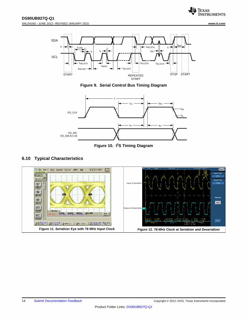
Figure 9. Serial Control Bus Timing Diagram
Figure 10. I2S Timing Diagram
6.10 Typical Characteristics
Figure 11. Serializer Eye with 78 MHz Input Clock Figure 12. 78-MHz Clock at Serializer and Deserializer
14 Submit Documentation Feedback Copyright © 2012–2015, Texas Instruments Incorporated
Product Folder Links: DS90UB927Q-Q1
PDB
PLL
Timing and Control
Ser
ial t
o P
aral
lel
Par
alle
l to
Ser
ial
DC
Bal
ance
Enc
oder
RxIN3±
SDA
SCL
IDx
LFMODE
RxIN2±
RxIN1±
RxIN0±
RxCLKIN±
MAPSEL
DOUT±
DOUT+
CMFREGULATOR
I2S / GPIO8
BKWD
REPEAT
INTB
DS90UB927Q-Q1www.ti.com SNLS416D –JUNE 2012–REVISED JANUARY 2015
7 Detailed Description
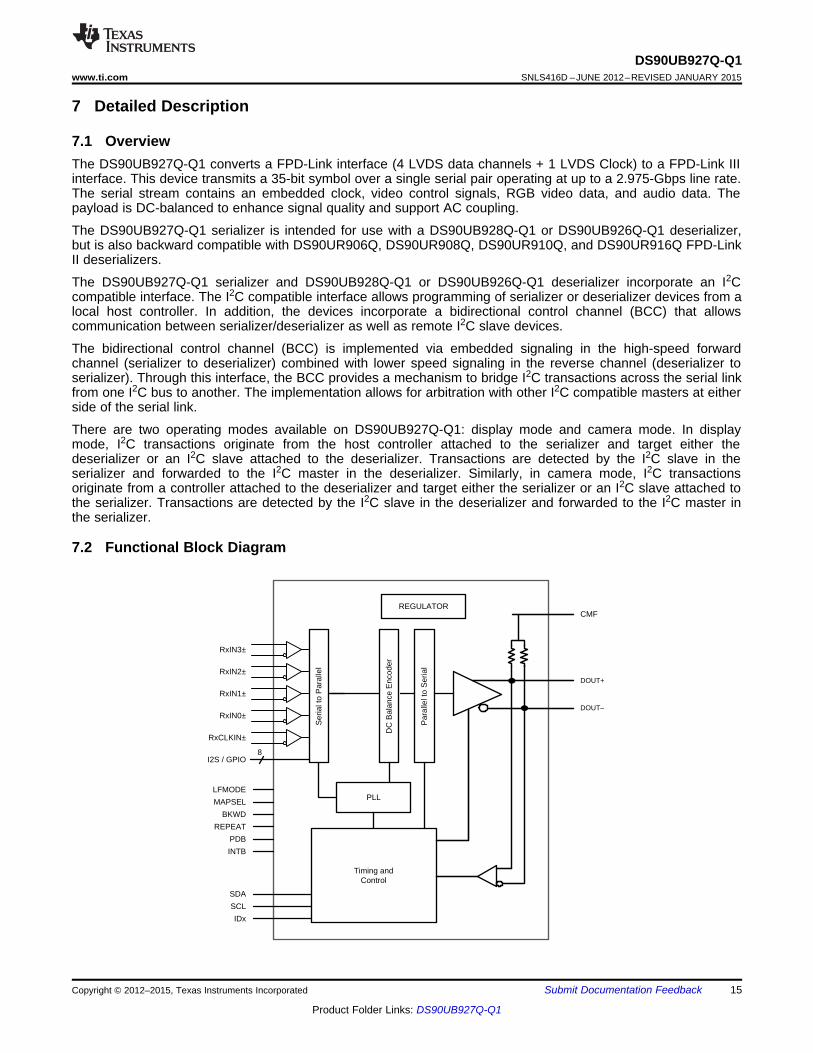
7.1 OverviewThe DS90UB927Q-Q1 converts a FPD-Link interface (4 LVDS data channels + 1 LVDS Clock) to a FPD-Link IIIinterface. This device transmits a 35-bit symbol over a single serial pair operating at up to a 2.975-Gbps line rate.The serial stream contains an embedded clock, video control signals, RGB video data, and audio data. Thepayload is DC-balanced to enhance signal quality and support AC coupling.
The DS90UB927Q-Q1 serializer is intended for use with a DS90UB928Q-Q1 or DS90UB926Q-Q1 deserializer,but is also backward compatible with DS90UR906Q, DS90UR908Q, DS90UR910Q, and DS90UR916Q FPD-LinkII deserializers.
The DS90UB927Q-Q1 serializer and DS90UB928Q-Q1 or DS90UB926Q-Q1 deserializer incorporate an I2Ccompatible interface. The I2C compatible interface allows programming of serializer or deserializer devices from alocal host controller. In addition, the devices incorporate a bidirectional control channel (BCC) that allowscommunication between serializer/deserializer as well as remote I2C slave devices.
The bidirectional control channel (BCC) is implemented via embedded signaling in the high-speed forwardchannel (serializer to deserializer) combined with lower speed signaling in the reverse channel (deserializer toserializer). Through this interface, the BCC provides a mechanism to bridge I2C transactions across the serial linkfrom one I2C bus to another. The implementation allows for arbitration with other I2C compatible masters at eitherside of the serial link.
There are two operating modes available on DS90UB927Q-Q1: display mode and camera mode. In displaymode, I2C transactions originate from the host controller attached to the serializer and target either thedeserializer or an I2C slave attached to the deserializer. Transactions are detected by the I2C slave in theserializer and forwarded to the I2C master in the deserializer. Similarly, in camera mode, I2C transactionsoriginate from a controller attached to the deserializer and target either the serializer or an I2C slave attached tothe serializer. Transactions are detected by the I2C slave in the deserializer and forwarded to the I2C master inthe serializer.
7.2 Functional Block Diagram
Copyright © 2012–2015, Texas Instruments Incorporated Submit Documentation Feedback 15
Product Folder Links: DS90UB927Q-Q1
C1 C0
DS90UB927Q-Q1SNLS416D –JUNE 2012–REVISED JANUARY 2015 www.ti.com
7.3 Feature Description
7.3.1 High-Speed Forward Channel Data TransferThe High Speed Forward Channel is composed of a 35-bit frame containing RGB data, sync signals, I2C, and I2Saudio transmitted from Serializer to Deserializer. Figure 13 illustrates the serial stream generated per PCLK cycleinto RxCLKIN±. This data payload is optimized for signal transmission over an AC coupled link. Data israndomized, DC-balanced and scrambled.
Figure 13. FPD-Link III Serial Stream
The device supports pixel clock ranges of 5 MHz to 15 MHz (LFMODE=1) and 15 MHz to 85 MHz (LFMODE=0).This corresponds to an application payload rate range of 155 Mbps to 2.635 Gbps, with an actual line rate rangeof 525 Mbps to 2.975 Gbps.
7.3.2 Low-Speed Back Channel Data TransferThe Low-Speed Back Channel of the DS90UB927Q-Q1 provides bidirectional communication between thedisplay and host processor. Data is transferred simultaneously over the same physical link as the high-speedforward channel data. The back channel transports I2C, CRC, and 4 bits of standard GPIO information with a 10-Mbps line rate.
7.3.3 Common Mode Filter Pin (CMF)The serializer provides access to the center tap of the internal CML termination. A 0.1-μF capacitor must beconnected from this pin to GND for additional common-mode filtering of the differential pair (Figure 29). Thisincreases noise rejection capability in high-noise environments.
7.3.4 Video Control SignalsThe video control signal bits embedded in the high-speed FPD-Link LVDS are subject to certain limitationsrelative to the video pixel clock period (PCLK). By default, the DS90UB927Q-Q1 applies a minimum pulse widthfilter on these signals to help eliminate spurious transitions.
Normal Mode Control Signals (VS, HS, DE) have the following restrictions:• Horizontal Sync (HS): The video control signal pulse width must be 3 PCLKs or longer when the Control
Signal Filter (register bit 0x03[4]) is enabled (default). Disabling the Control Signal Filter removes thisrestriction (minimum is 1 PCLK). See Table 5. HS can have at most two transitions per 130 PCLKs.
• Vertical Sync (VS): The video control signal pulse is limited to 1 transition per 130 PCLKs. Thus, the minimumpulse width is 130 PCLKs.
• Data Enable Input (DE): The video control signal pulse width must be 3 PCLKs or longer when the ControlSignal Filter (register bit 0x03[4]) is enabled (default). Disabling the Control Signal Filter removes thisrestriction (minimum is 1 PCLK). See Table 5. DE can have at most two transitions per 130 PCLKs.
7.3.5 EMI Reduction Features
7.3.5.1 LVCMOS VDDIO OptionThe 1.8-V or 3.3-V LVCMOS inputs and outputs are powered from separate VDDIO supply pins to offercompatibility with external system interface signals. Note: When configuring the VDDIO power supplies, all thesingle-ended control input pins for device need to scale together with the same operating VDDIO levels. If VDDIO isselected to operate in the 3.0 V to 3.6 V range, VDDIO must be operated within 300 mV of VDD33.
7.3.6 Built-In Self Test (BIST)An optional At-Speed Built-In Self Test (BIST) feature supports testing of the high speed serial link and the low-speed back channel without external data connections. This is useful in the prototype stage, equipmentproduction, in-system test, and system diagnostics.
16 Submit Documentation Feedback Copyright © 2012–2015, Texas Instruments Incorporated
Product Folder Links: DS90UB927Q-Q1
BISTstart
BISTstop
BISTWait
Step 1: DES in BIST
Step 2: Wait, SER in BIST
Step 3: DES in Normal Mode - check PASS
Step 4: DES/SER in Normal
Normal
DS90UB927Q-Q1www.ti.com SNLS416D –JUNE 2012–REVISED JANUARY 2015
Feature Description (continued)7.3.6.1 BIST Configuration and StatusThe BIST mode is enabled at the deserializer by pin (BISTEN) or BIST configuration register. The test mayselect either an external PCLK or the 33-MHz internal Oscillator clock (OSC) frequency. In the absence of PCLK,the user can select the internal OSC frequency at the deserializer through the BISTC pin or BIST configurationregister.
When BIST is activated at the deserializer, a BIST enable signal is sent to the serializer through the BackChannel. The serializer outputs a test pattern and drives the link at speed. The deserializer detects the testpattern and monitors it for errors. The deserializer PASS output pin toggles to flag each frame receivedcontaining one or more errors. The serializer also tracks errors indicated by the CRC fields in each back channelframe.
The BIST status can be monitored real time on the deserializer PASS pin, with each detected error resulting in ahalf pixel clock period toggled LOW. After BIST is deactivated, the result of the last test is held on the PASSoutput until reset (new BIST or Power Down). A high on PASS indicates NO ERRORS were detected. A Low onPASS indicates one or more errors were detected. The duration of the test is controlled by the pulse widthapplied to the deserializer BISTEN pin. LOCK is valid throughout the entire duration of BIST.
See Figure 14 for the BIST mode flow diagram.
7.3.6.2 Sample BIST SequenceStep 1: For the DS90UB927Q-Q1 paired with a FPD-Link III Deserializer, BIST Mode is enabled via the BISTENpin of Deserializer. The desired clock source is selected through the deserializer BISTC pin.
Step 2: The DS90UB927Q-Q1 serializer is awakened through the back channel if it is not already on. An all-zeros pattern is balanced, scrambled, randomized, and sent through the FPD-Link III interface to the deserializer.Once the serializer and the deserializer are in BIST mode and the deserializer acquires Lock, the PASS pin ofthe deserializer goes high and BIST starts checking the data stream. If an error in the payload (1 to 35) isdetected, the PASS pin will switch low for one half of the clock period. During the BIST, the PASS output can bemonitored and counted to determine the payload error rate.
Step 3: To Stop the BIST mode, the deserializer BISTEN pin is set Low. The deserializer stops checking thedata. The final test result is held on the PASS pin. If the test ran error free, the PASS output will remain HIGH. Ifthere one or more errors were detected, the PASS output will output constant LOW. The PASS output state isheld until a new BIST is run, the device is RESET, or the device is powered down. BIST duration is user-controlled and may be of any length.
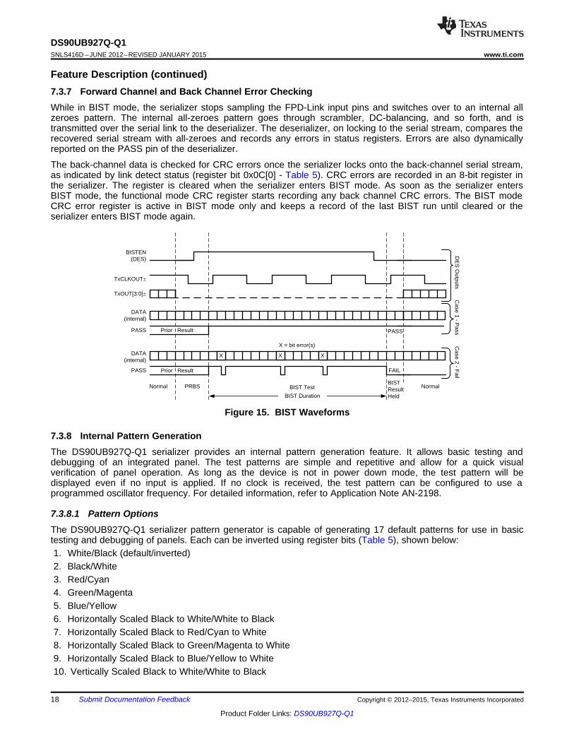
The link returns to normal operation after the deserializer BISTEN pin is low. Figure 15 shows the waveformdiagram of a typical BIST for two cases. Case 1 is error free, and Case 2 shows one with multiple errors. In mostcases it is difficult to generate errors due to the robustness of the link (differential data transmission, and soforth), thus they may be introduced by greatly extending the cable length, faulting the interconnect medium, orreducing signal condition enhancements (Rx Equalization).
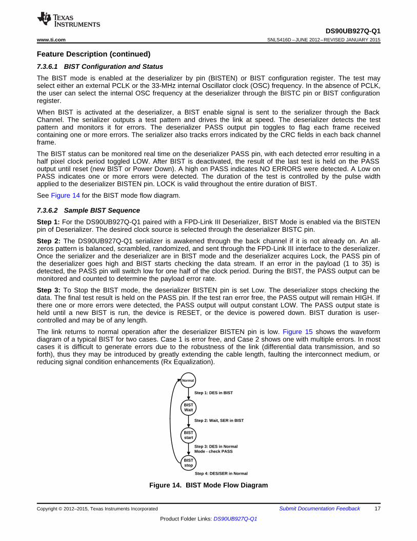
Figure 14. BIST Mode Flow Diagram
Copyright © 2012–2015, Texas Instruments Incorporated Submit Documentation Feedback 17
Product Folder Links: DS90UB927Q-Q1
X XX
TxCLKOUT±
BISTEN(DES)
PASS
DATA(internal)
PASS
BIST Duration
Prior Result
BIST ResultHeld
PASS
FAIL
X = bit error(s)
TxOUT[3:0]±
DATA(internal)
Case 1 - P
assC
ase 2 - Fail
Prior Result
Normal PRBS BIST Test Normal
DE
S O
utputs
DS90UB927Q-Q1SNLS416D –JUNE 2012–REVISED JANUARY 2015 www.ti.com
Feature Description (continued)7.3.7 Forward Channel and Back Channel Error CheckingWhile in BIST mode, the serializer stops sampling the FPD-Link input pins and switches over to an internal allzeroes pattern. The internal all-zeroes pattern goes through scrambler, DC-balancing, and so forth, and istransmitted over the serial link to the deserializer. The deserializer, on locking to the serial stream, compares therecovered serial stream with all-zeroes and records any errors in status registers. Errors are also dynamicallyreported on the PASS pin of the deserializer.
The back-channel data is checked for CRC errors once the serializer locks onto the back-channel serial stream,as indicated by link detect status (register bit 0x0C[0] - Table 5). CRC errors are recorded in an 8-bit register inthe serializer. The register is cleared when the serializer enters BIST mode. As soon as the serializer entersBIST mode, the functional mode CRC register starts recording any back channel CRC errors. The BIST modeCRC error register is active in BIST mode only and keeps a record of the last BIST run until cleared or theserializer enters BIST mode again.
Figure 15. BIST Waveforms
7.3.8 Internal Pattern GenerationThe DS90UB927Q-Q1 serializer provides an internal pattern generation feature. It allows basic testing anddebugging of an integrated panel. The test patterns are simple and repetitive and allow for a quick visualverification of panel operation. As long as the device is not in power down mode, the test pattern will bedisplayed even if no input is applied. If no clock is received, the test pattern can be configured to use aprogrammed oscillator frequency. For detailed information, refer to Application Note AN-2198.
7.3.8.1 Pattern OptionsThe DS90UB927Q-Q1 serializer pattern generator is capable of generating 17 default patterns for use in basictesting and debugging of panels. Each can be inverted using register bits (Table 5), shown below:1. White/Black (default/inverted)2. Black/White3. Red/Cyan4. Green/Magenta5. Blue/Yellow6. Horizontally Scaled Black to White/White to Black7. Horizontally Scaled Black to Red/Cyan to White8. Horizontally Scaled Black to Green/Magenta to White9. Horizontally Scaled Black to Blue/Yellow to White10. Vertically Scaled Black to White/White to Black
18 Submit Documentation Feedback Copyright © 2012–2015, Texas Instruments Incorporated
Product Folder Links: DS90UB927Q-Q1
DS90UB927Q-Q1www.ti.com SNLS416D –JUNE 2012–REVISED JANUARY 2015
Feature Description (continued)11. Vertically Scaled Black to Red/Cyan to White12. Vertically Scaled Black to Green/Magenta to White13. Vertically Scaled Black to Blue/Yellow to White14. Custom Color (or its inversion) configured in PGRS15. Black-White/White-Black Checkerboard (or custom checkerboard color, configured in PGCTL)16. YCBR/RBCY VCOM pattern, orientation is configurable from PGCTL17. Color Bars (White, Yellow, Cyan, Green, Magenta, Red, Blue, Black) – Note: not included in the auto-
scrolling feature
Additionally, the Pattern Generator incorporates one user-configurable full-screen 24-bit color, which is controlledby the PGRS, PGGS, and PGBS registers. This is pattern #14. One of the pattern options is statically selected inthe PGCTL register when Auto-Scrolling is disabled. The PGTSC and PGTSO1-8 registers control the patternselection and order when Auto-Scrolling is enabled.
7.3.8.2 Color ModesBy default, the Pattern Generator operates in 24-bit color mode, where all bits of the Red, Green, and Blueoutputs are enabled. 18-bit color mode can be activated from the configuration registers (Table 5). In 18-bitmode, the 6 most significant bits (bits 7-2) of the Red, Green, and Blue outputs are enabled; the 2 leastsignificant bits will be 0.
7.3.8.3 Video Timing ModesThe Pattern Generator has two video timing modes – external and internal. In external timing mode, the PatternGenerator detects the video frame timing present on the DE and VS inputs. If Vertical Sync signaling is notpresent on VS, the Pattern Generator determines Vertical Blank by detecting when the number of inactive pixelclocks (DE = 0) exceeds twice the detected active line length. In internal timing mode, the Pattern Generatoruses custom video timing as configured in the control registers. The internal timing generation may also bedriven by an external clock. By default, external timing mode is enabled. Internal timing or Internal timing withExternal Clock are enabled by the control registers (Table 5).
7.3.8.4 External TimingIn external timing mode, the Pattern Generator passes the incoming DE, HS, and VS signals unmodified to thevideo control outputs after a two pixel clock delay. It extracts the active frame dimensions from the incomingsignals in order to properly scale the brightness patterns. If the incoming video stream does not use the VSsignal, the Pattern Generator determines the Vertical Blank time by detecting a long period of pixel clocks withoutDE asserted.
7.3.8.5 Pattern InversionThe Pattern Generator also incorporates a global inversion control, located in the PGCFG register, which causesthe output pattern to be bitwise-inverted. For example, the full screen Red pattern becomes full-screen cyan, andthe Vertically Scaled Black to Green pattern becomes Vertically Scaled White to Magenta.
7.3.8.6 Auto ScrollingThe Pattern Generator supports an Auto-Scrolling mode, in which the output pattern cycles through a list ofenabled pattern types. A sequence of up to 16 patterns may be defined in the registers. The patterns mayappear in any order in the sequence and may also appear more than once.
Copyright © 2012–2015, Texas Instruments Incorporated Submit Documentation Feedback 19
Product Folder Links: DS90UB927Q-Q1
Normal Operation
Remote Auto Power Down Enabled
Forward-channel OFF
Sleep
DisableSet reg_0x01[7]=0
EnableSet reg_0x01[7]=1 Back Channel IDLE
Back Channel ACTIVE
DS90UB927Q-Q1SNLS416D –JUNE 2012–REVISED JANUARY 2015 www.ti.com
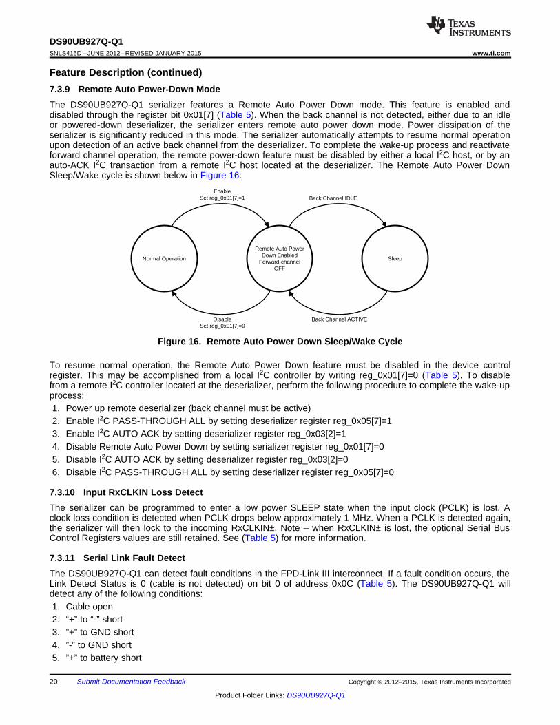
Feature Description (continued)7.3.9 Remote Auto Power-Down ModeThe DS90UB927Q-Q1 serializer features a Remote Auto Power Down mode. This feature is enabled anddisabled through the register bit 0x01[7] (Table 5). When the back channel is not detected, either due to an idleor powered-down deserializer, the serializer enters remote auto power down mode. Power dissipation of theserializer is significantly reduced in this mode. The serializer automatically attempts to resume normal operationupon detection of an active back channel from the deserializer. To complete the wake-up process and reactivateforward channel operation, the remote power-down feature must be disabled by either a local I2C host, or by anauto-ACK I2C transaction from a remote I2C host located at the deserializer. The Remote Auto Power DownSleep/Wake cycle is shown below in Figure 16:
Figure 16. Remote Auto Power Down Sleep/Wake Cycle
To resume normal operation, the Remote Auto Power Down feature must be disabled in the device controlregister. This may be accomplished from a local I2C controller by writing reg_0x01[7]=0 (Table 5). To disablefrom a remote I2C controller located at the deserializer, perform the following procedure to complete the wake-upprocess:1. Power up remote deserializer (back channel must be active)2. Enable I2C PASS-THROUGH ALL by setting deserializer register reg_0x05[7]=13. Enable I2C AUTO ACK by setting deserializer register reg_0x03[2]=14. Disable Remote Auto Power Down by setting serializer register reg_0x01[7]=05. Disable I2C AUTO ACK by setting deserializer register reg_0x03[2]=06. Disable I2C PASS-THROUGH ALL by setting deserializer register reg_0x05[7]=0
7.3.10 Input RxCLKIN Loss DetectThe serializer can be programmed to enter a low power SLEEP state when the input clock (PCLK) is lost. Aclock loss condition is detected when PCLK drops below approximately 1 MHz. When a PCLK is detected again,the serializer will then lock to the incoming RxCLKIN±. Note – when RxCLKIN± is lost, the optional Serial BusControl Registers values are still retained. See (Table 5) for more information.
7.3.11 Serial Link Fault DetectThe DS90UB927Q-Q1 can detect fault conditions in the FPD-Link III interconnect. If a fault condition occurs, theLink Detect Status is 0 (cable is not detected) on bit 0 of address 0x0C (Table 5). The DS90UB927Q-Q1 willdetect any of the following conditions:1. Cable open2. “+” to “-” short3. ”+” to GND short4. ”-” to GND short5. ”+” to battery short
20 Submit Documentation Feedback Copyright © 2012–2015, Texas Instruments Incorporated
Product Folder Links: DS90UB927Q-Q1
DS90UB927Q-Q1www.ti.com SNLS416D –JUNE 2012–REVISED JANUARY 2015
Feature Description (continued)6. ”-” to battery short7. Cable is linked incorrectly (DOUT+/DOUT- connections reversed)
Note: The device will detect any of the above conditions, but does not report specifically which one has occurred.
7.3.12 Interrupt Pin (INTB)1. On the DS90UB927Q-Q1 serializer, set register reg_0xC6[5] = 1 and 0xC6[0] = 1 (Table 5) to configure the
interrupt.2. On the serializer, read from ISR register 0xC7 to arm the interrupt for the first time.3. When INTB_IN on the deserializer (DS90UB926Q-Q1 or DS90UB928Q-Q1) is set LOW, the INTB pin on the
serializer also pulls low, indicating an interrupt condition.4. The external controller detects INTB = LOW and reads the ISR register (Table 5) to determine the interrupt
source. Reading this register also clears and resets the interrupt.
7.3.13 General-Purpose I/O
7.3.13.1 GPIO[3:0]In normal operation, GPIO[3:0] may be used as general purpose I/Os in either forward channel (inputs) or backchannel (outputs) applications. GPIO modes may be configured from the registers (Table 5). GPIO[1:0] arededicated pins and GPIO[3:2] are shared with I2S_DC and I2S_DD respectively. Note: if the DS90UB927Q-Q1 ispaired with a DS90UB926Q-Q1 deserializer, the devices must be configured into 18-bit mode to allow usage ofGPIO pins on the DS90UB927 serializer. To enable 18-bit mode, set serializer register reg_0x12[2] = 1. 18-bitmode will be auto-loaded into the deserializer from the serializer. See Table 1 for GPIO enable and configuration.
Table 1. GPIO Enable and ConfigurationDESCRIPTION DEVICE FORWARD CHANNEL BACK CHANNEL
DS90UB927Q-Q1 0x0F = 0x03 0x0F = 0x05GPIO3
DS90UB926/8Q-Q1 0x1F = 0x05 0x1F = 0x03DS90UB927Q-Q1 0x0E = 0x30 0x0E = 0x50
GPIO2DS90UB926/8Q-Q1 0x1E = 0x50 0x1E = 0x30DS90UB927Q-Q1 0x0E = 0x03 0x0E = 0x05
GPIO1DS90UB926/8Q-Q1 0x1E = 0x05 0x1E = 0x03DS90UB927Q-Q1 0x0D = 0x03 0x0D = 0x05
GPIO0DS90UB926/8Q-Q1 0x1D = 0x05 0x1D = 0x03
The input value present on GPIO[3:0] may also be read from register, or configured to local output mode(Table 5).
7.3.13.2 GPIO[8:5]GPIO_REG[8:5] are register-only GPIOs and may be programmed as outputs or read as inputs through localregister bits only. Where applicable, these bits are shared with I2S pins and will override I2S input if enabled intoREG_GPIO mode. See Table 2 for GPIO enable and configuration.
Note: Local GPIO value may be configured and read either through local register access, or remote registeraccess through the Low-Speed Bidirectional Control Channel. Configuration and state of these pins are nottransported from serializer to deserializer as is the case for GPIO[3:0].
Table 2. GPIO_REG and GPIO Local Enable and ConfigurationDESCRIPTION REGISTER CONFIGURATION FUNCTION
0x11 = 0x01 Output, LGPIO_REG8 0x11 = 0x09 Output, H
0x11 = 0x03 Input, Read: 0x1D[0]
Copyright © 2012–2015, Texas Instruments Incorporated Submit Documentation Feedback 21
Product Folder Links: DS90UB927Q-Q1
I2S_CLK
I2S_WC
I2S_Dx MSB LSB MSB LSB
Word Select
DS90UB927Q-Q1Bit Clock I2S_CLK
I2S_WCData I2S_Dx4
I2STransmitter
DS90UB927Q-Q1SNLS416D –JUNE 2012–REVISED JANUARY 2015 www.ti.com
Table 2. GPIO_REG and GPIO Local Enable and Configuration (continued)DESCRIPTION REGISTER CONFIGURATION FUNCTION
0x10 = 0x01 Output, LGPIO_REG7 0x10 = 0x09 Output, H
0x10 = 0x03 Input, Read: 0x1C[7]0x10 = 0x01 Output, L
GPIO_REG6 0x10 = 0x09 Output, H0x10 = 0x03 Input, Read: 0x1C[6]0x0F = 0x01 Output, L
GPIO_REG5 0x0F = 0x09 Output, H0x0F = 0x03 Input, Read: 0x1C[5]0x0F = 0x01 Output, L
GPIO3 0x0F = 0x09 Output, H0x0F = 0x03 Input, Read: 0x1C[3]0x0E = 0x01 Output, L
GPIO2 0x0E = 0x09 Output, H0x0E = 0x03 Input, Read: 0x1C[2]0x0E = 0x01 Output, L
GPIO1 0x0E = 0x09 Output, H0x0E = 0x03 Input, Read: 0x1C[1]0x0D = 0x01 Output, L
GPIO0 0x0D = 0x09 Output, H0x0D = 0x03 Input, Read: 0x1C[0]
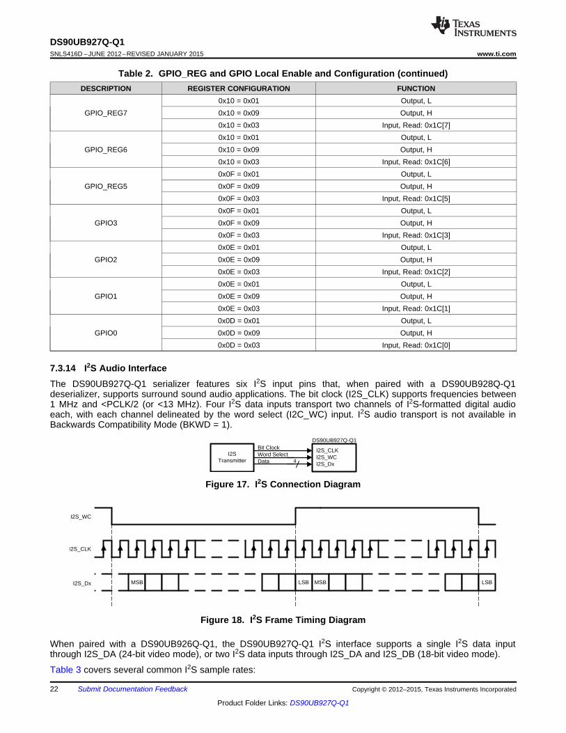
7.3.14 I2S Audio InterfaceThe DS90UB927Q-Q1 serializer features six I2S input pins that, when paired with a DS90UB928Q-Q1deserializer, supports surround sound audio applications. The bit clock (I2S_CLK) supports frequencies between1 MHz and <PCLK/2 (or <13 MHz). Four I2S data inputs transport two channels of I2S-formatted digital audioeach, with each channel delineated by the word select (I2C_WC) input. I2S audio transport is not available inBackwards Compatibility Mode (BKWD = 1).
Figure 17. I2S Connection Diagram
Figure 18. I2S Frame Timing Diagram
When paired with a DS90UB926Q-Q1, the DS90UB927Q-Q1 I2S interface supports a single I2S data inputthrough I2S_DA (24-bit video mode), or two I2S data inputs through I2S_DA and I2S_DB (18-bit video mode).
Table 3 covers several common I2S sample rates:
22 Submit Documentation Feedback Copyright © 2012–2015, Texas Instruments Incorporated
Product Folder Links: DS90UB927Q-Q1
DS90UB927Q-Q1www.ti.com SNLS416D –JUNE 2012–REVISED JANUARY 2015
Table 3. Audio Interface FrequenciesSample Rate (kHz) I2S Data Word Size (bits) I2S CLK (MHz)
32 16 1.02444.1 16 1.41148 16 1.53696 16 3.072192 16 6.14432 24 1.536
44.1 24 2.11748 24 2.30496 24 4.608192 24 9.21632 32 2.048
44.1 32 2.82248 32 3.07296 32 6.144192 32 12.288
7.3.14.1 I2S Transport ModesBy default, audio is packetized and transmitted during video blanking periods in dedicated Data Island Transportframes. Data Island frames may be disabled from control registers if Forward Channel Frame Transport of I2Sdata is desired. In this mode, only I2S_DA is transmitted to the DS90UB928Q-Q1 deserializer. If connected to aDS90UB926Q-Q1 deserializer, I2S_DA and I2S_DB are transmitted. Surround Sound Mode, which transmits allfour I2S data inputs (I2S_D[A..D]), may only be operated in Data Island Transport mode. This mode is onlyavailable when connected to a DS90UB928Q-Q1 deserializer.
7.3.14.2 I2S RepeaterI2S audio may be fanned-out and propagated in the repeater application. By default, data is propagated via DataIsland Transport on the FPD-Link interface during the video blanking periods. If frame transport is desired, thenthe I2S pins should be connected from the deserializer to all serializers. Activating surround sound at the top-level deserializer automatically configures downstream DS90UB927Q-Q1 serializers and DS90UB928Q-Q1deserializers for surround sound transport utilizing Data Island Transport. If 4-channel operation utilizing I2S_DAand I2S_DB only is desired, this mode must be explicitly set in each serializer and deserializer control registerthroughout the repeater tree (Table 5).
A DS90UB927Q-Q1 serializer configured in repeater mode may also regenerate I2S audio from its I2S input pinsin lieu of Data Island frames. See the Repeater Connection Diagram (Figure 23) and the I2C Control Registers(Table 5) for additional details.
7.3.15 Additional FeaturesAdditional pattern generator features can be accessed through the Pattern Generator Indirect Register Map. Itconsists of the Pattern Generator Indirect Address (PGIA reg_0x66 — Table 5) and the Pattern GeneratorIndirect Data (PGID reg_0x67 — Table 5). See TI application Note AN-2198.
7.4 Device Functional Modes
7.4.1 Power Down (PDB)The Serializer has a PDB input pin to ENABLE or POWER DOWN the device. This pin may be controlled by anexternal device, or through VDDIO, where VDDIO = 3.0 V to 3.6 V or VDD33. To save power, disable the link whenthe display is not needed (PDB = LOW). Ensure that this pin is not driven HIGH before VDD33 and VDDIO havereached final levels. When PDB is driven low, ensure that the pin is driven to 0 V for at least 1.5 ms beforereleasing or driving high. In the case where PDB is pulled up to VDDIO = 3.0 V to 3.6 V or VDD33 directly, a 10-kΩpullup resistor and a >10-µF capacitor to ground are required (See Figure 29).
Copyright © 2012–2015, Texas Instruments Incorporated Submit Documentation Feedback 23
Product Folder Links: DS90UB927Q-Q1
R[0](bit 21)
R[1](bit 22)
R[2](bit 0)
R[3](bit 1)
R[4](bit 2)
R[5](bit 3)
R[6](bit 4)
R[7](bit 5)
G[0](bit 23)
G[1](bit 24)
G[2](bit 6)
G[3](bit 7)
G[4](bit 8)
G[5](bit 9)
G[6](bit 10)
G[7](bit 11)
B[0](bit 25)
B[1](bit 26)
B[2](bit 12)
B[3](bit 13)
B[4](bit 14)
B[5](bit 15)
B[6](bit 16)
B[7](bit 17)
HS(bit 18)
VS(bit 19)
DE(bit 20)
Previous cycle Current cycle (PCLK Period)
RxCLKIN +/-
RxIN3 +/-
RxIN2 +/-
RxIN1 +/-
RxIN0 +/-
DS90UB927Q-Q1SNLS416D –JUNE 2012–REVISED JANUARY 2015 www.ti.com
Device Functional Modes (continued)Toggling PDB low will POWER DOWN the device and RESET all control registers to default. During this time,PDB must be held low for a minimum period of time. See AC Electrical Characteristics for more information.
7.4.2 Backward Compatible ModeThe DS90UB927Q-Q1 is also backward compatible to DS90UR906Q, DS90UR908Q FPD, and DS90UR916QFPD-Link II deserializers for PCLK frequencies ranging from 5MHz to 65MHz. It is also backward compatible withthe DS90UR910Q for PCLK frequencies ranging from 5 MHz to 75 MHz. The serializer transmits 28-bits of dataover a single serial FPD-Link II pair operating at a payload rate of 120 Mbps to 1.8 Gbps, corresponding to a linerate of 140 Mbps to 2.1 Gbps. The Backward Compatibility configuration can be selected through the BKWD pinor programmed through the configuration register (Table 5). The bidirectional control channel, bidirectionalGPIOs, I2S, and interrupt (INTB) are not active in this mode. However, local I2C access to the serializer is stillavailable. Note: PCLK frequency range in this mode is 15 MHz to 75 MHz for LFMODE=0 and 5 MHZ to <15MHz for LFMODE=1.
7.4.3 Low Frequency Optimization (LFMODE)The LFMODE is set via register (Table 5) or LFMODE Pin. This mode optimizes device operation for lower inputdata clock ranges supported by the serializer. If LFMODE is Low (LFMODE = 0, default), the RxCLKIN±frequency is between 15 MHz and 85 MHz. If LFMODE is High (LFMODE = 1), the RxCLKIN± frequency isbetween 5 MHz and <15 MHz. Note: when the device LFMODE is changed, a PDB reset is required. WhenLFMODE is high (LFMODE=1), the line rate relative to the input data rate is multiplied by four. Thus, for theoperating range of 5MHz to <15MHz, the line rate is 700Mbps to <2.1Gbps with an effective data payload of175Mbps to 525Mbps. Note: for Backwards Compatibility Mode (BKWD=1), the line rate relative to the input datarate remains the same.
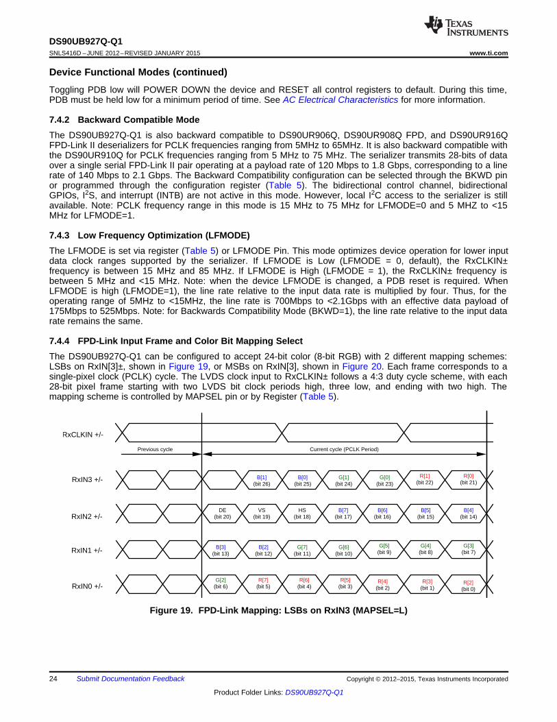
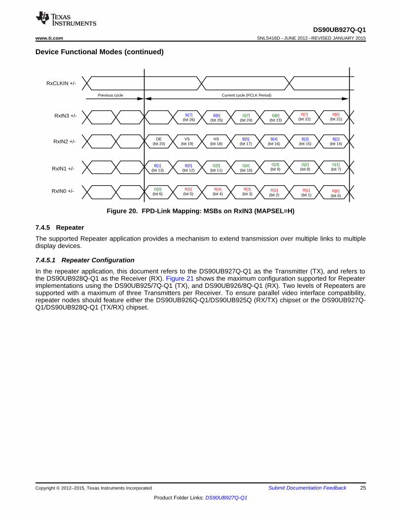
7.4.4 FPD-Link Input Frame and Color Bit Mapping SelectThe DS90UB927Q-Q1 can be configured to accept 24-bit color (8-bit RGB) with 2 different mapping schemes:LSBs on RxIN[3]±, shown in Figure 19, or MSBs on RxIN[3], shown in Figure 20. Each frame corresponds to asingle-pixel clock (PCLK) cycle. The LVDS clock input to RxCLKIN± follows a 4:3 duty cycle scheme, with each28-bit pixel frame starting with two LVDS bit clock periods high, three low, and ending with two high. Themapping scheme is controlled by MAPSEL pin or by Register (Table 5).
Figure 19. FPD-Link Mapping: LSBs on RxIN3 (MAPSEL=L)
24 Submit Documentation Feedback Copyright © 2012–2015, Texas Instruments Incorporated
Product Folder Links: DS90UB927Q-Q1
R[6](bit 21)
R[7](bit 22)
R[0](bit 0)
R[1](bit 1)
R[2](bit 2)
R[3](bit 3)
R[4](bit 4)
R[5](bit 5)
G[6](bit 23)
G[7](bit 24)
G[0](bit 6)
G[1](bit 7)
G[2](bit 8)
G[3](bit 9)
G[4](bit 10)
G[5](bit 11)
B[6](bit 25)
B[7](bit 26)
B[0](bit 12)
B[1](bit 13)
B[2](bit 14)
B[3](bit 15)
B[4](bit 16)
B[5](bit 17)
HS(bit 18)
VS(bit 19)
DE(bit 20)
Previous cycle Current cycle (PCLK Period)
RxCLKIN +/-
RxIN3 +/-
RxIN2 +/-
RxIN1 +/-
RxIN0 +/-
DS90UB927Q-Q1www.ti.com SNLS416D –JUNE 2012–REVISED JANUARY 2015
Device Functional Modes (continued)
Figure 20. FPD-Link Mapping: MSBs on RxIN3 (MAPSEL=H)
7.4.5 RepeaterThe supported Repeater application provides a mechanism to extend transmission over multiple links to multipledisplay devices.
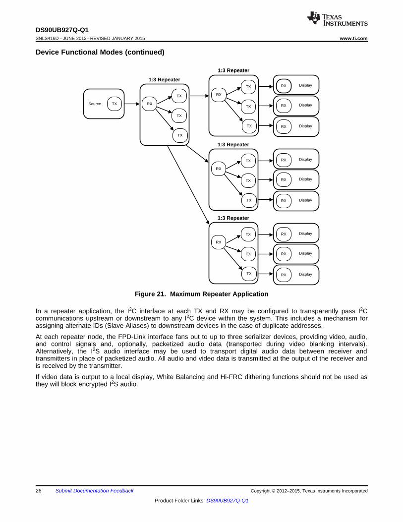
7.4.5.1 Repeater ConfigurationIn the repeater application, this document refers to the DS90UB927Q-Q1 as the Transmitter (TX), and refers tothe DS90UB928Q-Q1 as the Receiver (RX). Figure 21 shows the maximum configuration supported for Repeaterimplementations using the DS90UB925/7Q-Q1 (TX), and DS90UB926/8Q-Q1 (RX). Two levels of Repeaters aresupported with a maximum of three Transmitters per Receiver. To ensure parallel video interface compatibility,repeater nodes should feature either the DS90UB926Q-Q1/DS90UB925Q (RX/TX) chipset or the DS90UB927Q-Q1/DS90UB928Q-Q1 (TX/RX) chipset.
Copyright © 2012–2015, Texas Instruments Incorporated Submit Documentation Feedback 25
Product Folder Links: DS90UB927Q-Q1
TXSource
TX
TX
RX
1:3 Repeater
TX
TX
TX
RX
1:3 Repeater
TX
TX
TX
RX
1:3 Repeater
TX
TX
TX
RX
1:3 Repeater
TX
RX Display
RX Display
RX Display
RX Display
RX Display
RX Display
RX Display
RX Display
RX Display
DS90UB927Q-Q1SNLS416D –JUNE 2012–REVISED JANUARY 2015 www.ti.com
Device Functional Modes (continued)
Figure 21. Maximum Repeater Application
In a repeater application, the I2C interface at each TX and RX may be configured to transparently pass I2Ccommunications upstream or downstream to any I2C device within the system. This includes a mechanism forassigning alternate IDs (Slave Aliases) to downstream devices in the case of duplicate addresses.
At each repeater node, the FPD-Link interface fans out to up to three serializer devices, providing video, audio,and control signals and, optionally, packetized audio data (transported during video blanking intervals).Alternatively, the I2S audio interface may be used to transport digital audio data between receiver andtransmitters in place of packetized audio. All audio and video data is transmitted at the output of the receiver andis received by the transmitter.
If video data is output to a local display, White Balancing and Hi-FRC dithering functions should not be used asthey will block encrypted I2S audio.
26 Submit Documentation Feedback Copyright © 2012–2015, Texas Instruments Incorporated
Product Folder Links: DS90UB927Q-Q1
I2CMaster
upstreamTransmitter
HDCP TransmitterTX
I2CSlave
HDCP Receiver(RX)
FPD-Link
I2S Audio
I2C
HDCP TransmitterTX
I2CSlave
downstreamReceiverorRepeater
downstreamReceiverorRepeater
FPD-Link III interfaces
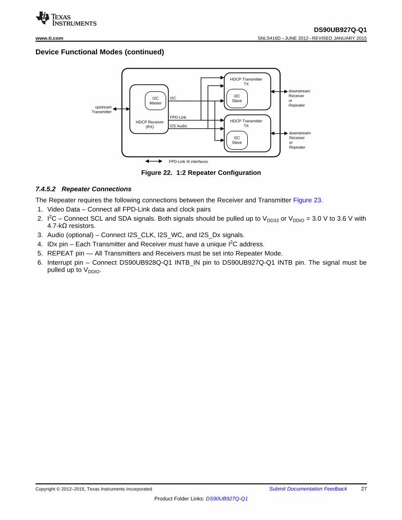
DS90UB927Q-Q1www.ti.com SNLS416D –JUNE 2012–REVISED JANUARY 2015
Device Functional Modes (continued)
Figure 22. 1:2 Repeater Configuration
7.4.5.2 Repeater ConnectionsThe Repeater requires the following connections between the Receiver and Transmitter Figure 23.1. Video Data – Connect all FPD-Link data and clock pairs2. I2C – Connect SCL and SDA signals. Both signals should be pulled up to VDD33 or VDDIO = 3.0 V to 3.6 V with
4.7-kΩ resistors.3. Audio (optional) – Connect I2S_CLK, I2S_WC, and I2S_Dx signals.4. IDx pin – Each Transmitter and Receiver must have a unique I2C address.5. REPEAT pin — All Transmitters and Receivers must be set into Repeater Mode.6. Interrupt pin – Connect DS90UB928Q-Q1 INTB_IN pin to DS90UB927Q-Q1 INTB pin. The signal must be
pulled up to VDDIO.
Copyright © 2012–2015, Texas Instruments Incorporated Submit Documentation Feedback 27
Product Folder Links: DS90UB927Q-Q1
DS90UB928Q-Q1
TxOUT0+
TxOUT0-
TxOUT1+
TxOUT1-
TxOUT2+
TxOUT2-
TxOUT3+
TxOUT3-
TxCLK+
TxCLK-
I2S_CLK
I2S_WC
I2S_Dx
INTB_IN
SDA
SCL
DS90UB927Q-Q1
RxIN0+
RxIN0-
RxIN1+
RxIN1-
RxIN2+
RxIN2-
RxIN3+
RxIN3-
RxCLK+
RxCLK-
I2S_CLK
I2S_WC
I2S_Dx
INTB
SDA
SCL
REPEAT
IDx
MODE_SEL
IDx
VDD33
VDD33
VDD33
VDD33
VDD33VDDIO
Optional
DS90UB927Q-Q1SNLS416D –JUNE 2012–REVISED JANUARY 2015 www.ti.com
Device Functional Modes (continued)
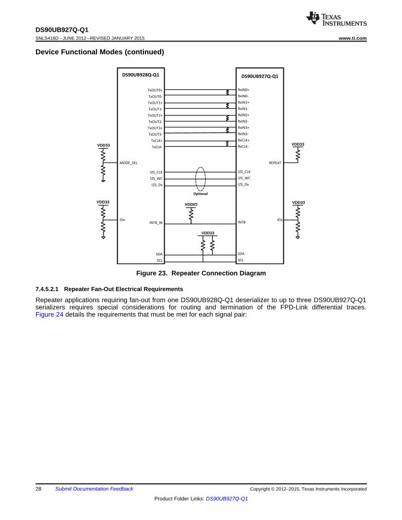
Figure 23. Repeater Connection Diagram
7.4.5.2.1 Repeater Fan-Out Electrical Requirements
Repeater applications requiring fan-out from one DS90UB928Q-Q1 deserializer to up to three DS90UB927Q-Q1serializers requires special considerations for routing and termination of the FPD-Link differential traces.Figure 24 details the requirements that must be met for each signal pair:
28 Submit Documentation Feedback Copyright © 2012–2015, Texas Instruments Incorporated
Product Folder Links: DS90UB927Q-Q1
HOST SER
SCL
SDA
4.7k 4.7k R2
SCL
SDA
To other Devices
IDx
VDD33
R1VDD33
VR2
RX(UB928)
TX(UB927)
TX(UB927)
TX(UB927)
R1=100 R2=100
L1 < 75 mm L2 < 60 mm
L3 < 60 mm
L3 < 60 mm
DS90UB927Q-Q1www.ti.com SNLS416D –JUNE 2012–REVISED JANUARY 2015
Device Functional Modes (continued)
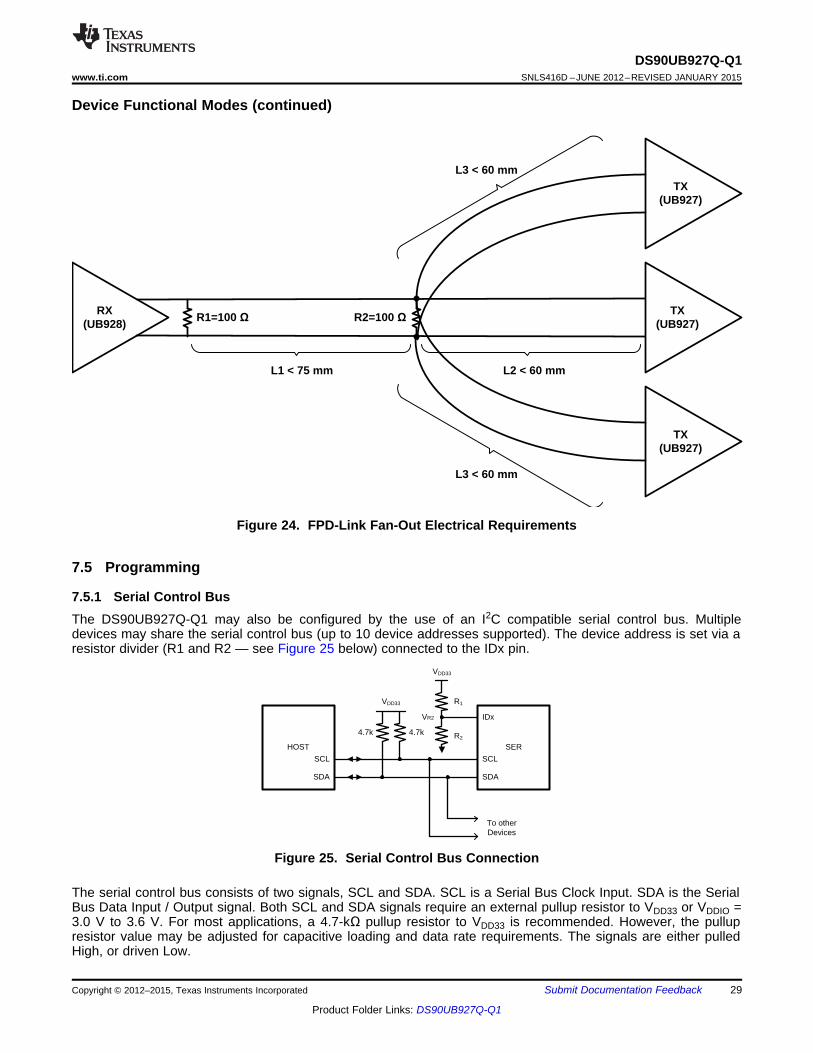
Figure 24. FPD-Link Fan-Out Electrical Requirements
7.5 Programming
7.5.1 Serial Control BusThe DS90UB927Q-Q1 may also be configured by the use of an I2C compatible serial control bus. Multipledevices may share the serial control bus (up to 10 device addresses supported). The device address is set via aresistor divider (R1 and R2 — see Figure 25 below) connected to the IDx pin.
Figure 25. Serial Control Bus Connection
The serial control bus consists of two signals, SCL and SDA. SCL is a Serial Bus Clock Input. SDA is the SerialBus Data Input / Output signal. Both SCL and SDA signals require an external pullup resistor to VDD33 or VDDIO =3.0 V to 3.6 V. For most applications, a 4.7-kΩ pullup resistor to VDD33 is recommended. However, the pullupresistor value may be adjusted for capacitive loading and data rate requirements. The signals are either pulledHigh, or driven Low.
Copyright © 2012–2015, Texas Instruments Incorporated Submit Documentation Feedback 29
Product Folder Links: DS90UB927Q-Q1
Slave Address Register Address Data
S 0ack
ack
ack P
A0
A1
A2
Slave Address Register Address Slave Address Data
S 0 1ack
ack
ack
ackS P
A0
A1
A2
A1
A2
A0
SDA
SCL
S PSTART condition, orSTART repeat condition
STOP condition
DS90UB927Q-Q1SNLS416D –JUNE 2012–REVISED JANUARY 2015 www.ti.com
Programming (continued)The IDx pin configures the control interface to one of 10 possible device addresses. A pullup resistor and apulldown resistor may be used to set the appropriate voltage ratio between the IDx input pin (VR2) and VDD33,each ratio corresponding to a specific device address. See Table 5 below.
Table 4. Serial Control Bus Addresses for IDxSuggested SuggestedIdeal Ratio Ideal VR2NO. Resistor R1 kΩ (1% Resistor R2 kΩ (1% Address 7'b Address 8'bVR2 / VDD33 (V) tol) tol)
1 0 0 Open 40.2 or >10 0x0C 0x182 0.306 1.011 221 97.6 0x13 0x263 0.350 1.154 210 113 0x14 0x284 0.393 1.298 196 127 0x15 0x2A5 0.440 1.452 182 143 0x16 0x2C6 0.483 1.594 169 158 0x17 0x2E7 0.529 1.745 147 165 0x18 0x308 0.572 1.887 143 191 0x19 0x329 0.618 2.040 121 196 0x1A 0x3410 0.768 2.535 90.9 301 0x1B 0x36
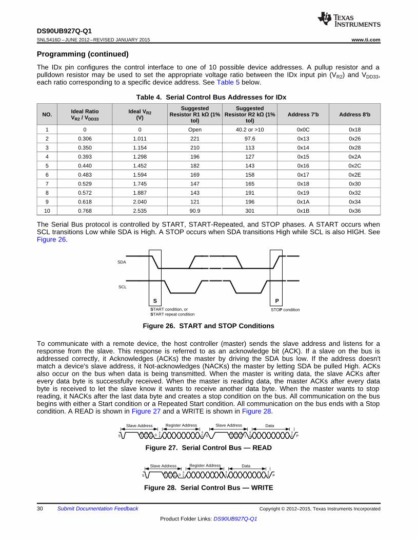
The Serial Bus protocol is controlled by START, START-Repeated, and STOP phases. A START occurs whenSCL transitions Low while SDA is High. A STOP occurs when SDA transitions High while SCL is also HIGH. SeeFigure 26.
Figure 26. START and STOP Conditions
To communicate with a remote device, the host controller (master) sends the slave address and listens for aresponse from the slave. This response is referred to as an acknowledge bit (ACK). If a slave on the bus isaddressed correctly, it Acknowledges (ACKs) the master by driving the SDA bus low. If the address doesn'tmatch a device's slave address, it Not-acknowledges (NACKs) the master by letting SDA be pulled High. ACKsalso occur on the bus when data is being transmitted. When the master is writing data, the slave ACKs afterevery data byte is successfully received. When the master is reading data, the master ACKs after every databyte is received to let the slave know it wants to receive another data byte. When the master wants to stopreading, it NACKs after the last data byte and creates a stop condition on the bus. All communication on the busbegins with either a Start condition or a Repeated Start condition. All communication on the bus ends with a Stopcondition. A READ is shown in Figure 27 and a WRITE is shown in Figure 28.
Figure 27. Serial Control Bus — READ
Figure 28. Serial Control Bus — WRITE
30 Submit Documentation Feedback Copyright © 2012–2015, Texas Instruments Incorporated
Product Folder Links: DS90UB927Q-Q1
DS90UB927Q-Q1www.ti.com SNLS416D –JUNE 2012–REVISED JANUARY 2015
The I2C Master located at the DS90UB927Q-Q1 serializer must support I2C clock stretching. For moreinformation on I2C interface requirements and throughput considerations, refer to TI Application Note SNLA131.
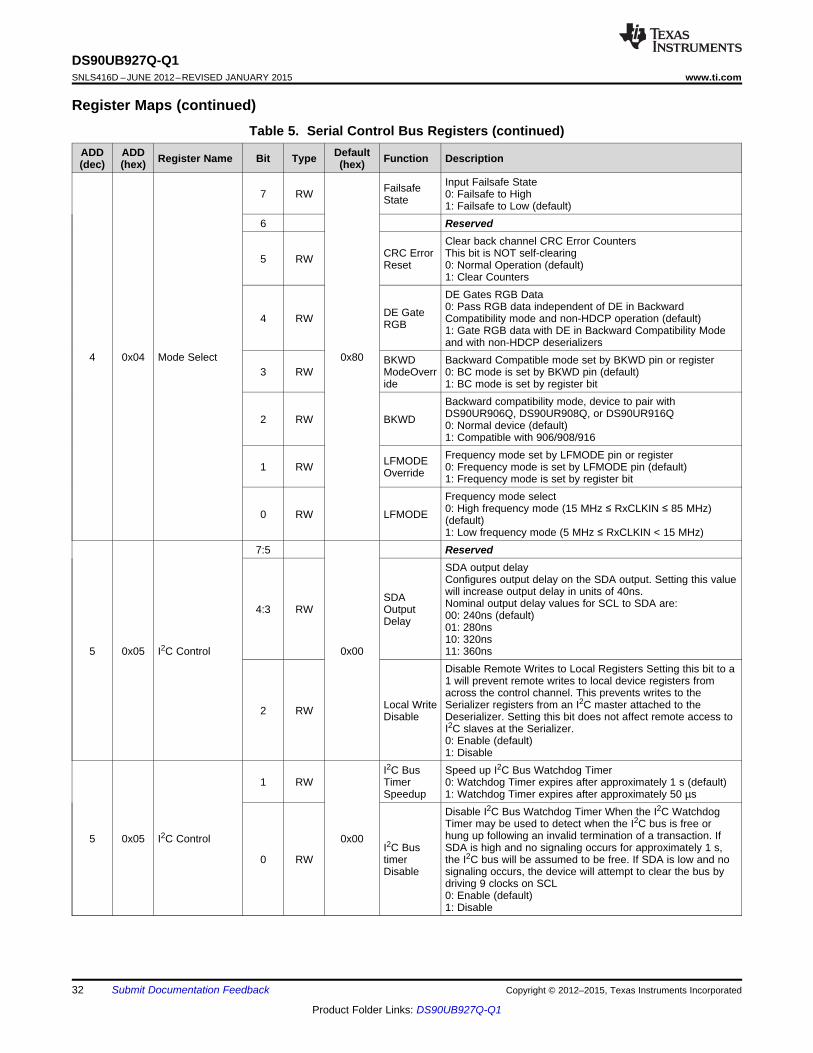
7.6 Register Maps
Table 5. Serial Control Bus RegistersADD ADD DefaultRegister Name Bit Type Function Description(dec) (hex) (hex)
7–bit address of Serializer7:1 RW Device ID Note: Read-only unless bit 0 is set0 0x00 I2C Device ID IDx I2C ID Setting
0 RW ID Setting 0: Device ID is from IDx pin1: Register I2C Device ID overrides IDx pinRemote Auto Power DownRemote 0: Do not power down when no Bidirectional Control ChannelAuto7 RW link is detected (default)Power 1: Enable power down when no Bidirectional Control ChannelDown link is detected
6:2 Reserved.Reset the entire digital block including registers1 0x01 Reset 0x00
Digital This bit is self-clearing.1 RW RESET1 0: Normal operation (default)1: ResetReset the entire digital block except registers
Digital This bit is self-clearing0 RW RESET0 0: Normal operation (default)1: Reset
Backchannel Back Channel Check Enable
7 RW CRC 0: DisableChecker 1: Enable (default)Enable
6 Reserved.Automatically Acknowledge I2C Remote Write When enabled,I2C writes to the Deserializer (or any remote I2C Slave, if I2C
I2C PASS ALL is enabled) are immediately acknowledged withoutRemote waiting for the Deserializer to acknowledge the write. This
5 RW Write Auto allows higher throughput on the I2C bus. Note: this mode willAcknowled prevent any NACK or read/write error indication from a
General ge remote device from reaching the I2C master.3 0x03 0xD2Configuration 0: Disable (default)1: EnableHS, VS, DE two clock filter When enabled, pulses less thantwo full PCLK cycles on the DE, HS, and VS inputs will beFilter4 RW rejectedEnable 0: Filtering disable1: Filtering enable (default)I2C Pass-Through ModeRead/Write transactions matching any entry in the
I2C Pass- DeviceAlias registers will be passed through to the remote3 RW through deserializer I2C interface.0: Pass-Through Disabled (default)1: Pass-Through Enabled
2 ReservedSwitch over to internal OSC in the absence of PCLKGeneral3 0x03 1 RW 0xD2 PCLK Auto 0: Disable auto-switchConfiguration 1: Enable auto-switch (default)
0 RW TRFB Reserved
Copyright © 2012–2015, Texas Instruments Incorporated Submit Documentation Feedback 31
Product Folder Links: DS90UB927Q-Q1
DS90UB927Q-Q1SNLS416D –JUNE 2012–REVISED JANUARY 2015 www.ti.com
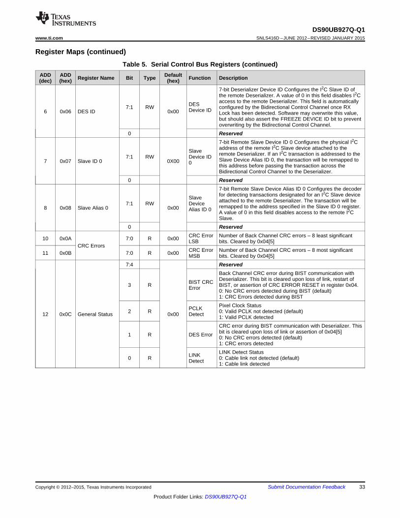
Register Maps (continued)Table 5. Serial Control Bus Registers (continued)
ADD ADD DefaultRegister Name Bit Type Function Description(dec) (hex) (hex)Input Failsafe StateFailsafe7 RW 0: Failsafe to HighState 1: Failsafe to Low (default)
6 ReservedClear back channel CRC Error Counters
CRC Error This bit is NOT self-clearing5 RW Reset 0: Normal Operation (default)1: Clear CountersDE Gates RGB Data0: Pass RGB data independent of DE in BackwardDE Gate4 RW Compatibility mode and non-HDCP operation (default)RGB 1: Gate RGB data with DE in Backward Compatibility Modeand with non-HDCP deserializers
4 0x04 Mode Select 0x80 BKWD Backward Compatible mode set by BKWD pin or register3 RW ModeOverr 0: BC mode is set by BKWD pin (default)
ide 1: BC mode is set by register bitBackward compatibility mode, device to pair withDS90UR906Q, DS90UR908Q, or DS90UR916Q2 RW BKWD 0: Normal device (default)1: Compatible with 906/908/916Frequency mode set by LFMODE pin or registerLFMODE1 RW 0: Frequency mode is set by LFMODE pin (default)Override 1: Frequency mode is set by register bitFrequency mode select0: High frequency mode (15 MHz ≤ RxCLKIN ≤ 85 MHz)0 RW LFMODE (default)1: Low frequency mode (5 MHz ≤ RxCLKIN < 15 MHz)
7:5 ReservedSDA output delayConfigures output delay on the SDA output. Setting this valuewill increase output delay in units of 40ns.SDA Nominal output delay values for SCL to SDA are:4:3 RW Output 00: 240ns (default)Delay 01: 280ns10: 320ns
5 0x05 I2C Control 0x00 11: 360nsDisable Remote Writes to Local Registers Setting this bit to a1 will prevent remote writes to local device registers fromacross the control channel. This prevents writes to the
Local Write Serializer registers from an I2C master attached to the2 RW Disable Deserializer. Setting this bit does not affect remote access toI2C slaves at the Serializer.0: Enable (default)1: Disable
I2C Bus Speed up I2C Bus Watchdog Timer1 RW Timer 0: Watchdog Timer expires after approximately 1 s (default)
Speedup 1: Watchdog Timer expires after approximately 50 µsDisable I2C Bus Watchdog Timer When the I2C WatchdogTimer may be used to detect when the I2C bus is free orhung up following an invalid termination of a transaction. If5 0x05 I2C Control 0x00
I2C Bus SDA is high and no signaling occurs for approximately 1 s,0 RW timer the I2C bus will be assumed to be free. If SDA is low and no
Disable signaling occurs, the device will attempt to clear the bus bydriving 9 clocks on SCL0: Enable (default)1: Disable
32 Submit Documentation Feedback Copyright © 2012–2015, Texas Instruments Incorporated
Product Folder Links: DS90UB927Q-Q1
DS90UB927Q-Q1www.ti.com SNLS416D –JUNE 2012–REVISED JANUARY 2015
Register Maps (continued)Table 5. Serial Control Bus Registers (continued)
ADD ADD DefaultRegister Name Bit Type Function Description(dec) (hex) (hex)7-bit Deserializer Device ID Configures the I2C Slave ID ofthe remote Deserializer. A value of 0 in this field disables I2Caccess to the remote Deserializer. This field is automaticallyDES7:1 RW configured by the Bidirectional Control Channel once RXDevice ID6 0x06 DES ID 0x00 Lock has been detected. Software may overwrite this value,but should also assert the FREEZE DEVICE ID bit to preventoverwriting by the Bidirectional Control Channel.
0 Reserved7-bit Remote Slave Device ID 0 Configures the physical I2Caddress of the remote I2C Slave device attached to theSlave remote Deserializer. If an I2C transaction is addressed to the7:1 RW Device ID Slave Device Alias ID 0, the transaction will be remapped to7 0x07 Slave ID 0 0X00 0 this address before passing the transaction across theBidirectional Control Channel to the Deserializer.
0 Reserved7-bit Remote Slave Device Alias ID 0 Configures the decoderfor detecting transactions designated for an I2C Slave deviceSlave attached to the remote Deserializer. The transaction will be7:1 RW Device remapped to the address specified in the Slave ID 0 register.8 0x08 Slave Alias 0 0x00 Alias ID 0 A value of 0 in this field disables access to the remote I2CSlave.
0 ReservedCRC Error Number of Back Channel CRC errors – 8 least significant10 0x0A 7:0 R 0x00 LSB bits. Cleared by 0x04[5]
CRC ErrorsCRC Error Number of Back Channel CRC errors – 8 most significant11 0x0B 7:0 R 0x00 MSB bits. Cleared by 0x04[5]
7:4 ReservedBack Channel CRC error during BIST communication withDeserializer. This bit is cleared upon loss of link, restart ofBIST CRC3 R BIST, or assertion of CRC ERROR RESET in register 0x04.Error 0: No CRC errors detected during BIST (default)1: CRC Errors detected during BISTPixel Clock StatusPCLK2 R 0: Valid PCLK not detected (default)12 0x0C General Status 0x00 Detect 1: Valid PCLK detectedCRC error during BIST communication with Deserializer. Thisbit is cleared upon loss of link or assertion of 0x04[5]1 R DES Error 0: No CRC errors detected (default)1: CRC errors detectedLINK Detect StatusLINK0 R 0: Cable link not detected (default)Detect 1: Cable link detected
Copyright © 2012–2015, Texas Instruments Incorporated Submit Documentation Feedback 33
Product Folder Links: DS90UB927Q-Q1
DS90UB927Q-Q1SNLS416D –JUNE 2012–REVISED JANUARY 2015 www.ti.com
Register Maps (continued)Table 5. Serial Control Bus Registers (continued)
ADD ADD DefaultRegister Name Bit Type Function Description(dec) (hex) (hex)Revision Revision ID:7:4 R ID 0010: Production Device
Local GPIO Output Value This value is output on the GPIOGPIO0 pin when the GPIO function is enabled, the local GPIO
3 RW Output direction is Output, and remote GPIO control is disabled.Value 0: Output LOW (default)
1: Output HIGHRemote GPIO Control
GPIO0 GPIO0 0: Disable GPIO control from remote Deserializer (default)13 0x0D 0x20Configuration 2 RW Remote 1: Enable GPIO control from remote Deserializer. The GPIOEnable pin will be an output, and the value is received from the
remote Deserializer.Local GPIO DirectionGPIO01 RW 0: Output (default)Direction 1: InputGPIO Function EnableGPIO00 RW 0: Enable normal operation (default)Enable 1: Enable GPIO operationLocal GPIO Output Value This value is output on the GPIO
GPIO2 pin when the GPIO function is enabled, the local GPIO7 RW Output direction is Output, and remote GPIO control is disabled.
Value 0: Output LOW (default)1: Output HIGHRemote GPIO Control
GPIO2 0: Disable GPIO control from remote Deserializer (default)6 RW Remote 1: Enable GPIO control from remote Deserializer. The GPIO
Enable pin will be an output, and the value is received from theremote Deserializer.Local GPIO DirectionGPIO25 RW 0: Output (default)Direction 1: InputGPIO Function EnableGPIO24 RW 0: Enable normal operation (default)EnableGPIO1 and 1: Enable GPIO operation
14 0x0E GPIO2 0x00Local GPIO Output Value This value is output on the GPIOConfiguration
GPIO1 pin when the GPIO function is enabled, the local GPIO3 RW Output direction is Output, and remote GPIO control is disabled.
Value 0: Output LOW (default)1: Output HIGHRemote GPIO Control
GPIO1 0: Disable GPIO control from remote Deserializer (default)2 RW Remote 1: Enable GPIO control from remote Deserializer. The GPIO
Enable pin will be an output, and the value is received from theremote Deserializer.Local GPIO DirectionGPIO11 RW 1: InputDirection 0: OutputGPIO function enableGPIO10 RW 1: Enable GPIO operationEnable 0: Enable normal operation
34 Submit Documentation Feedback Copyright © 2012–2015, Texas Instruments Incorporated
Product Folder Links: DS90UB927Q-Q1
DS90UB927Q-Q1www.ti.com SNLS416D –JUNE 2012–REVISED JANUARY 2015
Register Maps (continued)Table 5. Serial Control Bus Registers (continued)
ADD ADD DefaultRegister Name Bit Type Function Description(dec) (hex) (hex)7:4 Reserved
Local GPIO Output Value This value is output on the GPIOGPIO3 pin when the GPIO function is enabled, the local GPIO
3 RW Output direction is Output, and remote GPIO control is disabled.Value 0: Output LOW (default)
1: Output HIGHRemote GPIO Control
GPIO3 0: Disable GPIO control from remote Deserializer (default)GPIO315 0x0F 2 RW 0x00 Remote 1: Enable GPIO control from remote Deserializer. The GPIOConfiguration Enable pin will be an output, and the value is received from theremote Deserializer.Local GPIO DirectionGPIO31 RW 0: Output (default)Direction 1: InputGPIO Function EnableGPIO30 RW 0: Enable normal operation (default)Enable 1: Enable GPIO operationLocal GPIO Output Value This value is output on the GPIO
GPIO_RE pin when the GPIO function is enabled, and the local GPIO7 RW G6 Output direction is Output.
Value 0: Output LOW (default)1: Output HIGH
6 ReservedGPIO_RE Local GPIO Direction
5 RW G6 0: Output (default)Direction 1: Input
GPIO Function EnableGPIO_RE4 RW 0: Enable normal operation (default)GPIO_REG5 G6 Enable 1: Enable GPIO operationand16 0x10 0x00GPIO_REG6 Local GPIO Output Value This value is output on the GPIOConfiguration GPIO_RE pin when the GPIO function is enabled, and the local GPIO
3 RW G5 Output direction is Output.Value 0: Output LOW (default)
1: Output HIGH2 Reserved
GPIO_RE GPIO Function Enable1 RW G5 0: Enable normal operation (default)
Direction 1: Enable GPIO operationGPIO Function EnableGPIO_RE0 RW 0: Enable normal operation (default)G5 Enable 1: Enable GPIO operation
Copyright © 2012–2015, Texas Instruments Incorporated Submit Documentation Feedback 35
Product Folder Links: DS90UB927Q-Q1
DS90UB927Q-Q1SNLS416D –JUNE 2012–REVISED JANUARY 2015 www.ti.com
Register Maps (continued)Table 5. Serial Control Bus Registers (continued)
ADD ADD DefaultRegister Name Bit Type Function Description(dec) (hex) (hex)Local GPIO Output Value This value is output on the GPIO
GPIO_RE pin when the GPIO function is enabled, and the local GPIO7 RW G8 Output direction is Output.
Value 0: Output LOW (default)1: Output HIGH
6 ReservedGPIO_RE Local GPIO Direction
5 RW G8 0: Output (default)Direction 1: Input
GPIO Function EnableGPIO_RE4 RW 0: Enable normal operation (default)GPIO_REG7 G8 Enable 1: Enable GPIO operationand17 0x11 0x00GPIO_REG8 Local GPIO Output Value This value is output on the GPIOConfiguration GPIO_RE pin when the GPIO function is enabled, and the local GPIO
3 RW G7 Output direction is Output.Value 0: Output LOW (default)
1: Output HIGH2 Reserved
GPIO_RE Local GPIO Direction1 RW G7 0: Output (default)
Direction 1: InputGPIO Function EnableGPO_REG0 RW 0: Enable normal operation (default)7 Enable 1: Enable GPIO operation
7:6 ReservedThis bit indicates the polarity of the DE (Data Enable) signal.
5 RW DE Polarity 0: DE is positive (active high, idle low) (default)1: DE is inverted (active low, idle high)
I2S Regenerate I2S Data From Repeater I2S Pins4 RW Repeater 0: Repeater pass through I2S from video pins (default)
Regen 1: Repeater regenerate I2S from I2S pinsI2S I2S Channel B OverrideChannel B3 RW 0: Set I2S Channel B Disabled (default)Data Path Enable18 0x12 0x00 1: Set I2S Channel B Enable from reg_12[0]Control Override18-bit Video Color Depth Mode
2 RW Video 0: Select 24-bit video mode (default)Select 1: Select 18-bit video modeI2S Select I2S Transport Mode
1 RW Transport 0: Enable I2S Data Island Transport (default)Select 1: Enable I2S Data Forward Channel Frame TransportI2S I2S Channel B Enable
0 RW Channel B 0: I2S Channel B disabled (default)Enable 1: Enable I2S Channel B
36 Submit Documentation Feedback Copyright © 2012–2015, Texas Instruments Incorporated
Product Folder Links: DS90UB927Q-Q1
DS90UB927Q-Q1www.ti.com SNLS416D –JUNE 2012–REVISED JANUARY 2015
Register Maps (continued)Table 5. Serial Control Bus Registers (continued)
ADD ADD DefaultRegister Name Bit Type Function Description(dec) (hex) (hex)MAPSEL7 R Returns Map Select Mode (MAPSEL) pin statusMode
FPD-Link Map Select (MAPSEL) set by input pin or registerMAPSEL6 RW 0: Map Select is set by input pin (default)Override 1: Map Select is set by register bit 0x13[5]FPD-Link Map Select (MAPSEL) value when 0x13[6] is setMAPSEL5 RW 0: LSBs on RxIN3± (default)Value 1: MSBs on RxIN3±
4 ReservedLow Frequency Mode (LFMODE) pin statusGeneral Purpose LFMODE19 0x13 0x103 R 0: 15 ≤ RxCLKIN ≤ 85MHz (default)Control Status 1: 5 ≤ RxCLKIN < 15MHzRepeater Mode (REPEAT) pin StatusREPEAT2 R 0: Non-repeater (default)Status 1: RepeaterBackward Compatible Mode (BKWD) StatusBKWD1 R 0: Compatible to DS90UB926/8Q-Q1 (default)Status 1: Backward compatible to DS90UR906/8Q-Q1I2S Channel B Mode (I2S_DB) StatusI2S_DB0 R 0: I2S_DB inactive (default)Status 1: I2S_DB active
7:3 ReservedInternal OSC clock select for Functional Mode or BIST.Functional Mode when PCLK is not present and 0x03[1]=1.00: 33 MHz Oscillator (default)
OSC Clock 01: 33 MHz Oscillator2:1 RW Source Clock Source in BIST mode20 0x14 BIST Control 0x00 00: External Pixel Clock (default)01: 33 MHz OscillatorNote: In LFMODE=1, the internal oscillator is 12.5MHzBIST ControlBIST0 R 0: Disabled (default)Enable 1: EnabledThe watchdog timer allows termination of a control channeltransaction if it fails to complete within a programmed amountTimer7:1 RW of time. This field sets the Bidirectional Control ChannelValue Watchdog Timeout value in units of 2 milliseconds. This fieldBCC Watchdog22 0x16 0xFE should not be set to 0.ControlDisable BCC Watchdog TimerTimer0 RW 0: Enable BCC Watchdog Timer operation (default)Control 1: Disable BCC Watchdog Timer operationPass All0: Enable Forward Control Channel pass-through only of I2Caccesses to I2C Slave IDs matching either the remoteI2C Pass7 RW Deserializer Slave ID or the remote Slave ID. (default)All 1: Enable Forward Control Channel pass-through of all I2Caccesses to I2C Slave IDs that do not match the SerializerI2C Slave ID.
23 0x17 I2C Control 0x1E Internal SDA Hold TimeSDA Hold Configures the amount of internal hold time provided for the6:4 RW Time SDA input relative to the SCL input. Units are 40
nanoseconds.Configures the maximum width of glitch pulses on the SCLI2C Filter3:0 RW and SDA inputs that will be rejected. Units are 5Depth nanoseconds.
Copyright © 2012–2015, Texas Instruments Incorporated Submit Documentation Feedback 37
Product Folder Links: DS90UB927Q-Q1
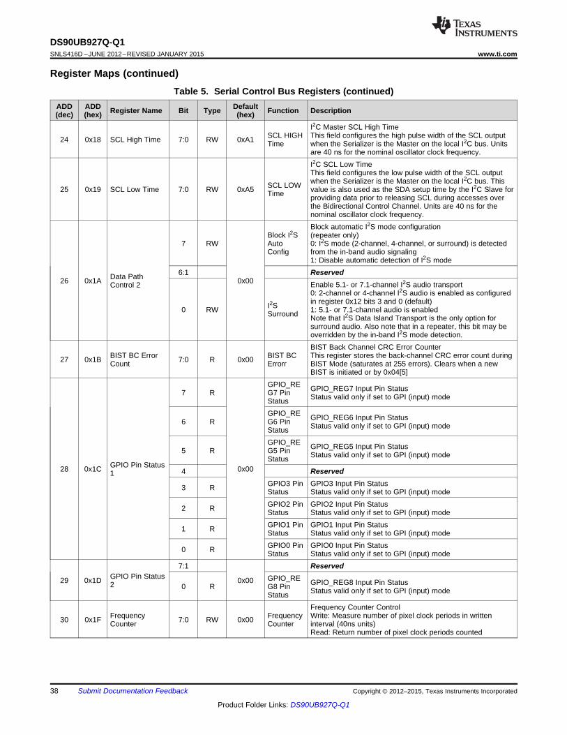
DS90UB927Q-Q1SNLS416D –JUNE 2012–REVISED JANUARY 2015 www.ti.com
Register Maps (continued)Table 5. Serial Control Bus Registers (continued)
ADD ADD DefaultRegister Name Bit Type Function Description(dec) (hex) (hex)I2C Master SCL High Time
SCL HIGH This field configures the high pulse width of the SCL output24 0x18 SCL High Time 7:0 RW 0xA1 Time when the Serializer is the Master on the local I2C bus. Unitsare 40 ns for the nominal oscillator clock frequency.I2C SCL Low TimeThis field configures the low pulse width of the SCL outputwhen the Serializer is the Master on the local I2C bus. ThisSCL LOW25 0x19 SCL Low Time 7:0 RW 0xA5 value is also used as the SDA setup time by the I2C Slave forTime providing data prior to releasing SCL during accesses overthe Bidirectional Control Channel. Units are 40 ns for thenominal oscillator clock frequency.Block automatic I2S mode configuration
Block I2S (repeater only)7 RW Auto 0: I2S mode (2-channel, 4-channel, or surround) is detected
Config from the in-band audio signaling1: Disable automatic detection of I2S mode
6:1 ReservedData Path26 0x1A 0x00 Enable 5.1- or 7.1-channel I2S audio transportControl 20: 2-channel or 4-channel I2S audio is enabled as configuredin register 0x12 bits 3 and 0 (default)I2S0 RW 1: 5.1- or 7.1-channel audio is enabledSurround Note that I2S Data Island Transport is the only option forsurround audio. Also note that in a repeater, this bit may beoverridden by the in-band I2S mode detection.BIST Back Channel CRC Error Counter
BIST BC Error BIST BC This register stores the back-channel CRC error count during27 0x1B 7:0 R 0x00Count Errorr BIST Mode (saturates at 255 errors). Clears when a newBIST is initiated or by 0x04[5]
GPIO_RE GPIO_REG7 Input Pin Status7 R G7 Pin Status valid only if set to GPI (input) modeStatusGPIO_RE GPIO_REG6 Input Pin Status6 R G6 Pin Status valid only if set to GPI (input) modeStatusGPIO_RE GPIO_REG5 Input Pin Status5 R G5 Pin Status valid only if set to GPI (input) modeStatus
GPIO Pin Status28 0x1C 0x004 Reserved1GPIO3 Pin GPIO3 Input Pin Status3 R Status Status valid only if set to GPI (input) modeGPIO2 Pin GPIO2 Input Pin Status2 R Status Status valid only if set to GPI (input) modeGPIO1 Pin GPIO1 Input Pin Status1 R Status Status valid only if set to GPI (input) modeGPIO0 Pin GPIO0 Input Pin Status0 R Status Status valid only if set to GPI (input) mode
7:1 ReservedGPIO Pin Status GPIO_RE29 0x1D 0x00 GPIO_REG8 Input Pin Status2 0 R G8 Pin Status valid only if set to GPI (input) modeStatus
Frequency Counter ControlFrequency Frequency Write: Measure number of pixel clock periods in written30 0x1F 7:0 RW 0x00Counter Counter interval (40ns units)
Read: Return number of pixel clock periods counted
38 Submit Documentation Feedback Copyright © 2012–2015, Texas Instruments Incorporated
Product Folder Links: DS90UB927Q-Q1
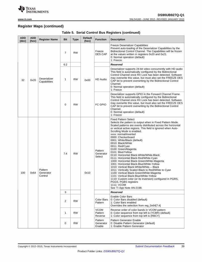
DS90UB927Q-Q1www.ti.com SNLS416D –JUNE 2012–REVISED JANUARY 2015
Register Maps (continued)Table 5. Serial Control Bus Registers (continued)
ADD ADD DefaultRegister Name Bit Type Function Description(dec) (hex) (hex)Freeze Deserializer CapabilitiesPrevent auto-loading of the Deserializer Capabilities by the
Freeze Bidirectional Control Channel. The Capabilities will be frozen7 RW DES CAP at the values written in registers 0x20 and 0x21.0: Normal operation (default)1: Freeze
6:2 ReservedDeserializer supports 24-bit video concurrently with HD audioThis field is automatically configured by the BidirectionalControl Channel once RX Lock has been detected. Softwaremay overwrite this value, but must also set the FREEZE DESDeserializer 1 RW HD Audio32 0x20 0x00 CAP bit to prevent overwriting by the Bidirectional ControlCapabilitiesChannel.0: Normal operation (default)1: FreezeDeserializer supports GPIO in the Forward Channel FrameThis field is automatically configured by the BidirectionalControl Channel once RX Lock has been detected. Softwaremay overwrite this value, but must also set the FREEZE DES0 RW FC GPIO CAP bit to prevent overwriting by the Bidirectional ControlChannel.0: Normal operation (default)1: FreezeFixed Pattern SelectSelects the pattern to output when in Fixed Pattern Mode.Scaled patterns are evenly distributed across the horizontalor vertical active regions. This field is ignored when Auto-Scrolling Mode is enabled.xxxx: normal/inverted0000: Checkerboard0001: White/Black (default)0010: Black/White0011: Red/Cyan0100: Green/MagentaPattern 0101: Blue/Yellow7:4 RW Generator 0110: Horizontal Black-White/White-BlackSelect 0111: Horizontal Black-Red/White-Cyan1000: Horizontal Black-Green/White-Magenta1001: Horizontal Black-Blue/White-Yellow1010: Vertical Black-White/White— Black
Pattern 1011: Vertically Scaled Black to Red/White to Cyan100 0x64 Generator 0x10 1100: Vertical Black-Green/White-Magenta
Control 1101: Vertical Black-Blue/White-Yellow1110: Custom color (or its inversion) configured in PGRS,PGGS, PGBS registers1111: VCOMSee TI App Note AN-2198.
3 ReservedEnable Color Bars
Color Bars 0: Color Bars disabled (default)2 RW Pattern 1: Color Bars enabledOverrides the selection from reg_0x64[7:4]
VCOM Reverse order of color bands in VCOM pattern1 RW Pattern 0: Color sequence from top left is (YCBR) (default)
Reverse 1: Color sequence from top left is (RBCY)Pattern Pattern Generator Enable
0 RW Generator 0: Disable Pattern Generator (default)Enable 1: Enable Pattern Generator
Copyright © 2012–2015, Texas Instruments Incorporated Submit Documentation Feedback 39
Product Folder Links: DS90UB927Q-Q1
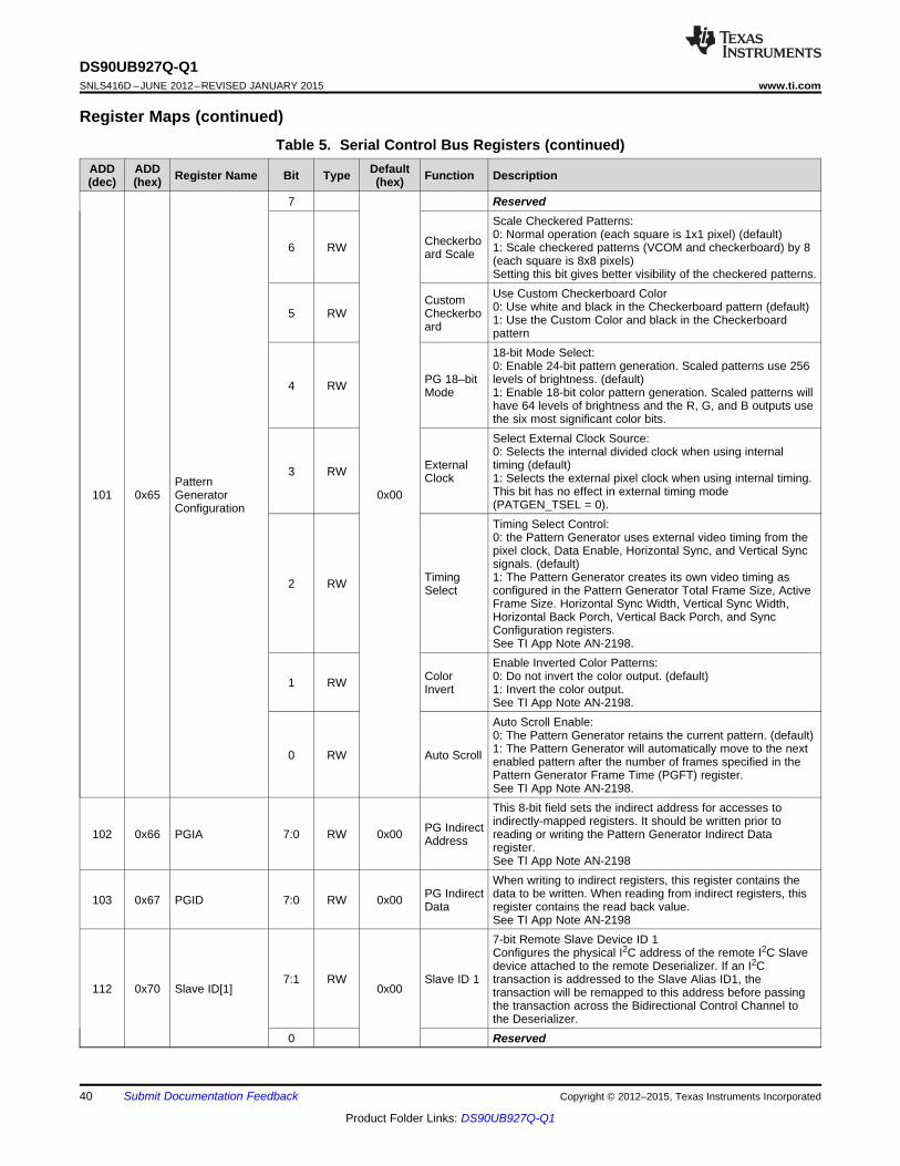
DS90UB927Q-Q1SNLS416D –JUNE 2012–REVISED JANUARY 2015 www.ti.com
Register Maps (continued)Table 5. Serial Control Bus Registers (continued)
ADD ADD DefaultRegister Name Bit Type Function Description(dec) (hex) (hex)7 Reserved
Scale Checkered Patterns:0: Normal operation (each square is 1x1 pixel) (default)Checkerbo6 RW 1: Scale checkered patterns (VCOM and checkerboard) by 8ard Scale (each square is 8x8 pixels)Setting this bit gives better visibility of the checkered patterns.Use Custom Checkerboard ColorCustom 0: Use white and black in the Checkerboard pattern (default)5 RW Checkerbo 1: Use the Custom Color and black in the Checkerboardard pattern18-bit Mode Select:0: Enable 24-bit pattern generation. Scaled patterns use 256
PG 18–bit levels of brightness. (default)4 RW Mode 1: Enable 18-bit color pattern generation. Scaled patterns willhave 64 levels of brightness and the R, G, and B outputs usethe six most significant color bits.Select External Clock Source:0: Selects the internal divided clock when using internal
External timing (default)3 RW Clock 1: Selects the external pixel clock when using internal timing.PatternThis bit has no effect in external timing mode101 0x65 Generator 0x00(PATGEN_TSEL = 0).ConfigurationTiming Select Control:0: the Pattern Generator uses external video timing from thepixel clock, Data Enable, Horizontal Sync, and Vertical Syncsignals. (default)
Timing 1: The Pattern Generator creates its own video timing as2 RW Select configured in the Pattern Generator Total Frame Size, ActiveFrame Size. Horizontal Sync Width, Vertical Sync Width,Horizontal Back Porch, Vertical Back Porch, and SyncConfiguration registers.See TI App Note AN-2198.Enable Inverted Color Patterns:
Color 0: Do not invert the color output. (default)1 RW Invert 1: Invert the color output.See TI App Note AN-2198.Auto Scroll Enable:0: The Pattern Generator retains the current pattern. (default)1: The Pattern Generator will automatically move to the next0 RW Auto Scroll enabled pattern after the number of frames specified in thePattern Generator Frame Time (PGFT) register.See TI App Note AN-2198.This 8-bit field sets the indirect address for accesses toindirectly-mapped registers. It should be written prior toPG Indirect102 0x66 PGIA 7:0 RW 0x00 reading or writing the Pattern Generator Indirect DataAddress register.See TI App Note AN-2198When writing to indirect registers, this register contains the
PG Indirect data to be written. When reading from indirect registers, this103 0x67 PGID 7:0 RW 0x00 Data register contains the read back value.See TI App Note AN-21987-bit Remote Slave Device ID 1Configures the physical I2C address of the remote I2C Slavedevice attached to the remote Deserializer. If an I2C
7:1 RW Slave ID 1 transaction is addressed to the Slave Alias ID1, the112 0x70 Slave ID[1] 0x00 transaction will be remapped to this address before passing
the transaction across the Bidirectional Control Channel tothe Deserializer.
0 Reserved
40 Submit Documentation Feedback Copyright © 2012–2015, Texas Instruments Incorporated
Product Folder Links: DS90UB927Q-Q1
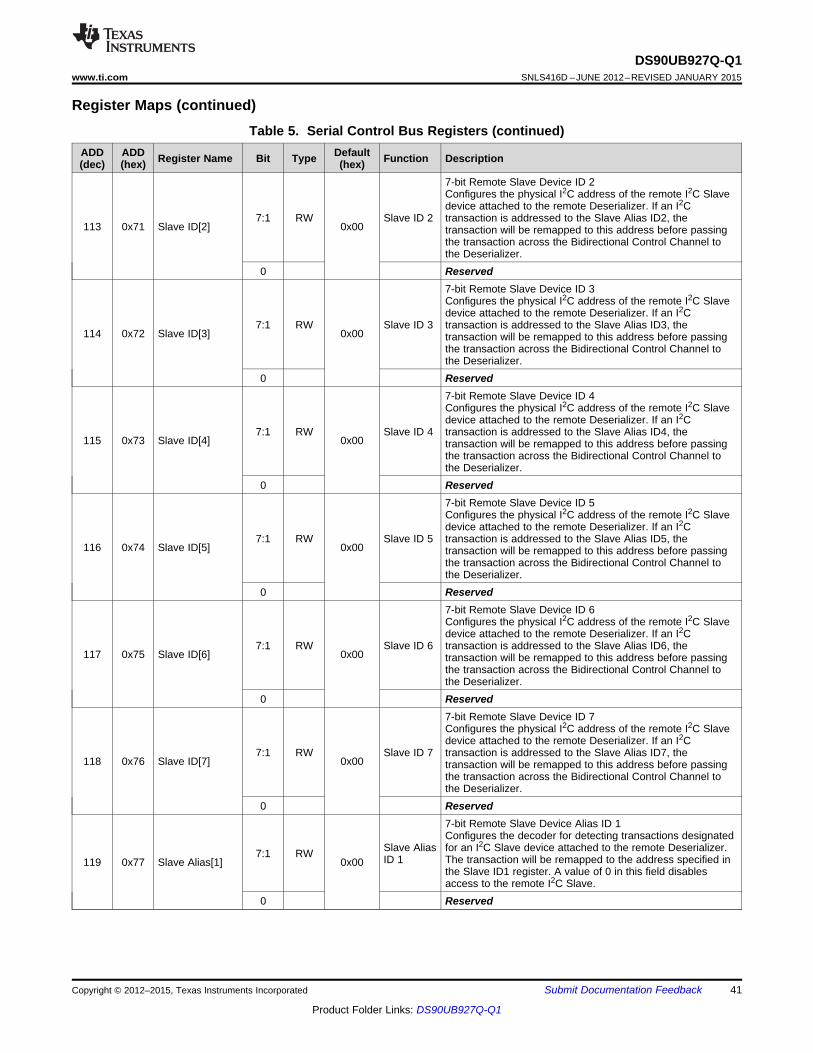
DS90UB927Q-Q1www.ti.com SNLS416D –JUNE 2012–REVISED JANUARY 2015
Register Maps (continued)Table 5. Serial Control Bus Registers (continued)
ADD ADD DefaultRegister Name Bit Type Function Description(dec) (hex) (hex)7-bit Remote Slave Device ID 2Configures the physical I2C address of the remote I2C Slavedevice attached to the remote Deserializer. If an I2C
7:1 RW Slave ID 2 transaction is addressed to the Slave Alias ID2, the113 0x71 Slave ID[2] 0x00 transaction will be remapped to this address before passing
the transaction across the Bidirectional Control Channel tothe Deserializer.
0 Reserved7-bit Remote Slave Device ID 3Configures the physical I2C address of the remote I2C Slavedevice attached to the remote Deserializer. If an I2C
7:1 RW Slave ID 3 transaction is addressed to the Slave Alias ID3, the114 0x72 Slave ID[3] 0x00 transaction will be remapped to this address before passing
the transaction across the Bidirectional Control Channel tothe Deserializer.
0 Reserved7-bit Remote Slave Device ID 4Configures the physical I2C address of the remote I2C Slavedevice attached to the remote Deserializer. If an I2C
7:1 RW Slave ID 4 transaction is addressed to the Slave Alias ID4, the115 0x73 Slave ID[4] 0x00 transaction will be remapped to this address before passing
the transaction across the Bidirectional Control Channel tothe Deserializer.
0 Reserved7-bit Remote Slave Device ID 5Configures the physical I2C address of the remote I2C Slavedevice attached to the remote Deserializer. If an I2C
7:1 RW Slave ID 5 transaction is addressed to the Slave Alias ID5, the116 0x74 Slave ID[5] 0x00 transaction will be remapped to this address before passing
the transaction across the Bidirectional Control Channel tothe Deserializer.
0 Reserved7-bit Remote Slave Device ID 6Configures the physical I2C address of the remote I2C Slavedevice attached to the remote Deserializer. If an I2C
7:1 RW Slave ID 6 transaction is addressed to the Slave Alias ID6, the117 0x75 Slave ID[6] 0x00 transaction will be remapped to this address before passing
the transaction across the Bidirectional Control Channel tothe Deserializer.
0 Reserved7-bit Remote Slave Device ID 7Configures the physical I2C address of the remote I2C Slavedevice attached to the remote Deserializer. If an I2C
7:1 RW Slave ID 7 transaction is addressed to the Slave Alias ID7, the118 0x76 Slave ID[7] 0x00 transaction will be remapped to this address before passing
the transaction across the Bidirectional Control Channel tothe Deserializer.
0 Reserved7-bit Remote Slave Device Alias ID 1Configures the decoder for detecting transactions designated
Slave Alias for an I2C Slave device attached to the remote Deserializer.7:1 RW ID 1 The transaction will be remapped to the address specified in119 0x77 Slave Alias[1] 0x00the Slave ID1 register. A value of 0 in this field disablesaccess to the remote I2C Slave.
0 Reserved
Copyright © 2012–2015, Texas Instruments Incorporated Submit Documentation Feedback 41
Product Folder Links: DS90UB927Q-Q1
DS90UB927Q-Q1SNLS416D –JUNE 2012–REVISED JANUARY 2015 www.ti.com
Register Maps (continued)Table 5. Serial Control Bus Registers (continued)
ADD ADD DefaultRegister Name Bit Type Function Description(dec) (hex) (hex)7-bit Remote Slave Device Alias ID 2Configures the decoder for detecting transactions designated
Slave Alias for an I2C Slave device attached to the remote Deserializer.7:1 RW ID 2 The transaction will be remapped to the address specified in120 0x78 Slave Alias[2] 0x00the Slave ID2 register. A value of 0 in this field disablesaccess to the remote I2C Slave.
0 Reserved7-bit Remote Slave Device Alias ID 3Configures the decoder for detecting transactions designated
Slave Alias for an I2C Slave device attached to the remote Deserializer.7:1 RW ID 3 The transaction will be remapped to the address specified in121 0x79 Slave Alias[3] 0x00the Slave ID3 register. A value of 0 in this field disablesaccess to the remote I2C Slave.
0 Reserved7-bit Remote Slave Device Alias ID 4Configures the decoder for detecting transactions designated
Slave Alias for an I2C Slave device attached to the remote Deserializer.7:1 RW ID 4 The transaction will be remapped to the address specified in122 0x7A Slave Alias[4] 0x00the Slave ID4 register. A value of 0 in this field disablesaccess to the remote I2C Slave.
0 Reserved7-bit Remote Slave Device Alias ID 5Configures the decoder for detecting transactions designated
Slave Alias for an I2C Slave device attached to the remote Deserializer.7:1 RW ID 5 The transaction will be remapped to the address specified in123 0x7B Slave Alias[5] 0x00the Slave ID5 register. A value of 0 in this field disablesaccess to the remote I2C Slave.
0 Reserved7-bit Remote Slave Device Alias ID 6Configures the decoder for detecting transactions designated
Slave Alias for an I2C Slave device attached to the remote Deserializer.7:1 RW ID 6 The transaction will be remapped to the address specified in124 0x7C Slave Alias[6] 0x00the Slave ID6 register. A value of 0 in this field disablesaccess to the remote I2C Slave.
0 Reserved7-bit Remote Slave Device Alias ID 7Configures the decoder for detecting transactions designated
Slave Alias for an I2C Slave device attached to the remote Deserializer.7:1 RW ID 7 The transaction will be remapped to the address specified in125 0x7D Slave Alias[7] 0x00the Slave ID7 register. A value of 0 in this field disablesaccess to the remote I2C Slave.
0 Reserved7:6 Reserved
Interrupt on Receiver interruptIS_RX_IN198 0xC6 ICR 5 RW 0x00 Enables interrupt on indication from the Receiver. AllowsT propagation of interrupts from downstream devices4:1 Reserved7:6 Reserved
Interrupt on Receiver interrupt5 R IS RX INT Receiver has indicated an interrupt request from downstream
device199 0xC7 ISR 0x004:1 Reserved
Global Interrupt Enable0 R INT Enable Set if any enabled interrupt is indicated
42 Submit Documentation Feedback Copyright © 2012–2015, Texas Instruments Incorporated
Product Folder Links: DS90UB927Q-Q1
DS90UB927Q-Q1www.ti.com SNLS416D –JUNE 2012–REVISED JANUARY 2015
Register Maps (continued)Table 5. Serial Control Bus Registers (continued)
ADD ADD DefaultRegister Name Bit Type Function Description(dec) (hex) (hex)240 0xF0 7:0 R 0x5F ID0 First byte ID code, ‘_’241 0xF1 7:0 R 0x55 ID1 Second byte of ID code, ‘U’242 0xF2 7:0 R 0x42 ID2 Third byte of ID code. ‘B’
TX ID243 0xF3 7:0 R 0x39 ID3 Forth byte of ID code: ‘9’244 0xF4 7:0 R 0x32 ID4 Fifth byte of ID code: “2”245 0xF5 7:0 R 0x37 ID5 Sixth byte of ID code: “7”
Copyright © 2012–2015, Texas Instruments Incorporated Submit Documentation Feedback 43
Product Folder Links: DS90UB927Q-Q1
DS90UB927Q-Q1SNLS416D –JUNE 2012–REVISED JANUARY 2015 www.ti.com
8 Application and Implementation
NOTEInformation in the following applications sections is not part of the TI componentspecification, and TI does not warrant its accuracy or completeness. TI’s customers areresponsible for determining suitability of components for their purposes. Customers shouldvalidate and test their design implementation to confirm system functionality.
8.1 Application InformationThe DS90UB927Q-Q1, in conjunction with the DS90UB928Q-Q1 or DS90UB926Q-Q1, is intended for interfacebetween a host (graphics processor) and a display, supporting 24-bit color depth (RGB888) and high definition(720p) digital video format. It can receive an 8-bit RGB stream with a pixel clock rate up to 85 MHz together withthree control bits (VS, HS and DE) and four I2S audio streams.
8.2 Typical ApplicationFigure 29 shows a typical application of the DS90UB927Q-Q1 serializer for an 85-MHz 24-bit Color DisplayApplication. The 5 LVDS input pairs require external 100Ω terminations. The CML outputs must have an external0.1-µF AC coupling capacitor on the high speed serial lines. The serializer has internal CML termination on itshigh speed outputs.
Bypass capacitors should be placed near the power supply pins. At a minimum, four (4) 4.7-µF capacitors shouldbe used for local device bypassing. Ferrite beads are placed on the two sets of supply pins (VDD33 and VDDIO)for effective noise suppression. The interface to the graphics source is LVDS. The VDDIO pins may beconnected to 3.3 V or 1.8 V. A capacitor and resistor are placed on the PDB pin to delay the enabling of thedevice until power is stable.
44 Submit Documentation Feedback Copyright © 2012–2015, Texas Instruments Incorporated
Product Folder Links: DS90UB927Q-Q1
PDB
CAPL12
CMF
DAP (GND)
CAPP12 CAPHS12
VDD33_A
3.3V (VDD33)DS90UB927Q-Q1
C5
C1
C2
Notes:FB1-FB2: Impedance = 1k:@100MHz Low DC resistance (<1:)
C1-C3 = 0.1 PF(50 WV; C1, C2: 0402; C3: 0603)C4-C12 = 4.7 PFC13 = >10 PFR1/R2: see IDx Resistor Value TableR4 = 10k:R5= 4.7k:
FPD-LinkInterface
SerialFPD-Link IIIInterface
INTB
I2S_CLKI2S_WCI2S_Dx
SCLSDA
IDx
3.3V or 1.8V (VDDIO)
RESx
C6
C13
VDDIO
FB1 FB2C4
C3
VDD33
4.7K
4.7K
R2
R1R4
VDD33
C10
VDDIO VDD33_B
CAPLVD12
RxCLKIN-
RxCLKIN+
RxIN3-
RxIN3+
RxIN2-
RxIN2+
RxIN1-
RxIN1+
RxIN0-
RxIN0+
4
LVCMOSControl
Interface
VDDIO
R5
100:
100:
100:
100:
100:
C11 C8 C9
C12
C7
MAPSEL
BKWD
LFMODE
REPEAT
DOUT+
DOUT-
DS90UB927Q-Q1www.ti.com SNLS416D –JUNE 2012–REVISED JANUARY 2015
Typical Application (continued)
Figure 29. Color Display Typical Connection Diagram
8.2.1 Design RequirementsFor the typical design application, use the following as input parameters.
Table 6. Design ParametersDESIGN PARAMETER EXAMPLE VALUE
VDDIO 1.8 V or 3.3 VVDD33 3.3 V
AC Coupling Capacitor for DOUT± 100 nFPCLK Frequency 85 MHz
8.2.2 Detailed Design ProcedureFigure 29 shows a typical application of the DS90UB927Q-Q1 serializer for an 85-MHz 24-bit Color DisplayApplication. The CML outputs must have an external 0.1-μF AC coupling capacitor on the high speed serial lines.Bypass capacitors are placed near the power supply pins. At a minimum, six 4.7-μF capacitors and twoadditional 1-μF capacitors should be used for local device bypassing. Ferrite beads are placed on the two VDDs(VDD33 and VDDIO) for effective noise suppression. An RC delay is placed on the PDB signal to delay theenabling of the device until power is stable.
Copyright © 2012–2015, Texas Instruments Incorporated Submit Documentation Feedback 45
Product Folder Links: DS90UB927Q-Q1
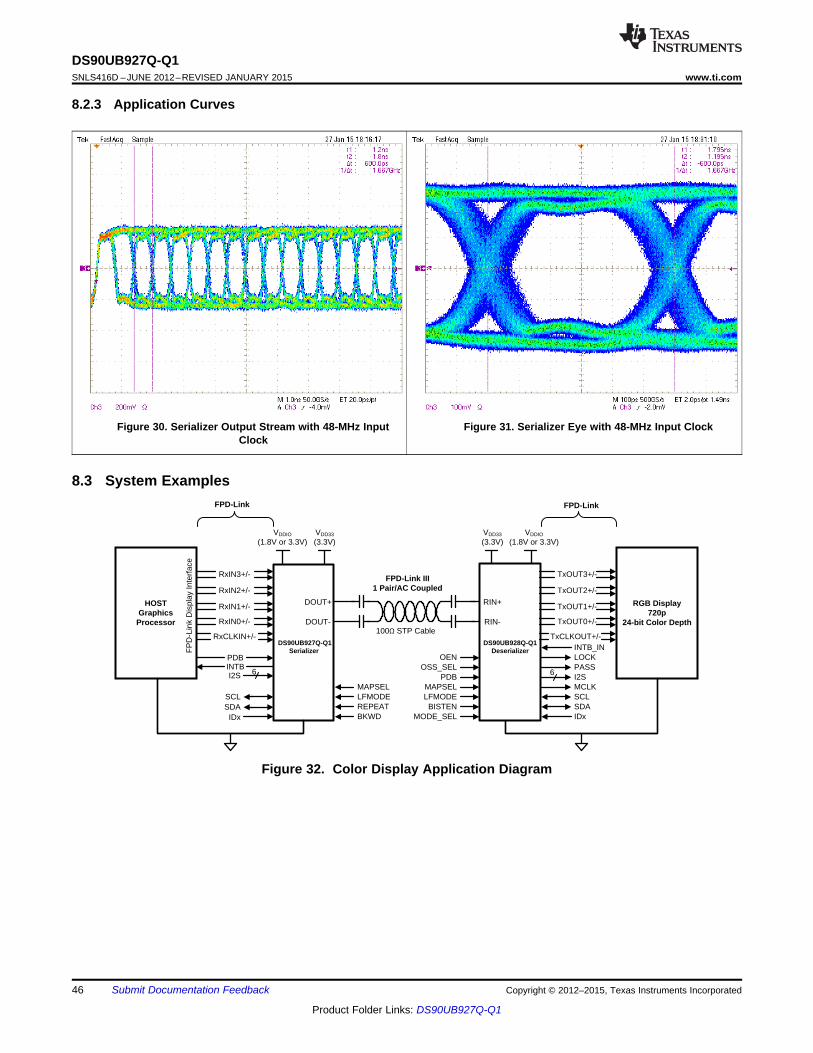
100Q STP Cable
FP
D-L
ink
Dis
play
Inte
rfac
e
RGB Display720p
24-bit Color Depth
DS90UB927Q-Q1Serializer
DS90UB928Q-Q1Deserializer
FPD-Link III 1 Pair/AC Coupled
VDDIO (1.8V or 3.3V)
FPD-LinkFPD-Link
RxIN1+/-
RxCLKIN+/-
RxIN2+/-
RxIN0+/-
RxIN3+/-
TxOUT1+/-
TxCLKOUT+/-
TxOUT2+/-
TxOUT0+/-
TxOUT3+/-
VDDIO (1.8V or 3.3V)
HOSTGraphics
Processor
DOUT+
DOUT-
RIN+
RIN-
SDASCL
I2SMCLK
66
VDD33 (3.3V)
VDD33 (3.3V)
MODE_SELBISTEN
LFMODEMAPSEL
PDBOSS_SEL
OEN
BKWDREPEATLFMODEMAPSEL
IDxSDASCL
LOCKPASS
PDBINTBI2S
INTB_IN
IDx
DS90UB927Q-Q1SNLS416D –JUNE 2012–REVISED JANUARY 2015 www.ti.com
8.2.3 Application Curves
Figure 30. Serializer Output Stream with 48-MHz Input Figure 31. Serializer Eye with 48-MHz Input ClockClock
8.3 System Examples
Figure 32. Color Display Application Diagram
46 Submit Documentation Feedback Copyright © 2012–2015, Texas Instruments Incorporated
Product Folder Links: DS90UB927Q-Q1
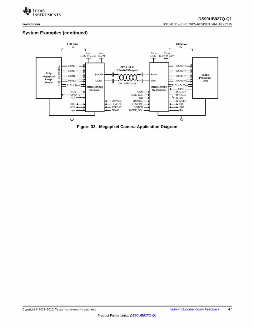
100Q STP Cable
FP
D-L
ink
Inte
rfac
e
ImageProcessor
Unit
DS90UB927QSerializer
DS90UB928QDeserializer
FPD-Link III 1 Pair/AC Coupled
VDDIO (1.8V or 3.3V)
FPD-LinkFPD-Link
RxIN1+/-
RxCLKIN+/-
RxIN2+/-
RxIN0+/-
RxIN3+/-
TxOUT1+/-
TxCLKOUT+/-
TxOUT2+/-
TxOUT0+/-
TxOUT3+/-
VDDIO (1.8V or 3.3V)
720pMegapixel
ImageSensor
DOUT+
DOUT-
RIN+
RIN-
SDASCL
I2SMCLK
66
VDD33 (3.3V)
VDD33 (3.3V)
MODE_SELBISTEN
LFMODEMAPSEL
PDBOSS_SEL
OEN
BKWDREPEATLFMODEMAPSEL
IDxSDASCL
LOCKPASS
PDBGPIOI2S
IDx
GPIO
DS90UB927Q-Q1www.ti.com SNLS416D –JUNE 2012–REVISED JANUARY 2015
System Examples (continued)
Figure 33. Megapixel Camera Application Diagram
Copyright © 2012–2015, Texas Instruments Incorporated Submit Documentation Feedback 47
Product Folder Links: DS90UB927Q-Q1
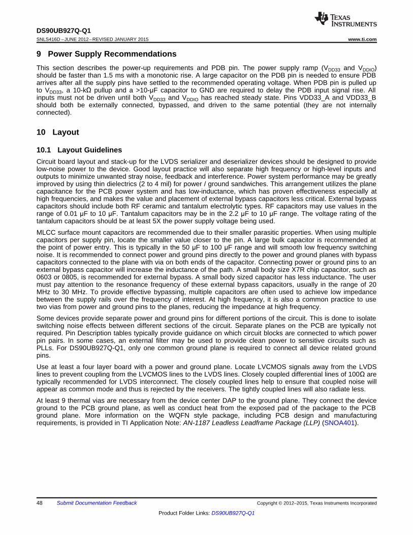
DS90UB927Q-Q1SNLS416D –JUNE 2012–REVISED JANUARY 2015 www.ti.com
9 Power Supply RecommendationsThis section describes the power-up requirements and PDB pin. The power supply ramp (VDD33 and VDDIO)should be faster than 1.5 ms with a monotonic rise. A large capacitor on the PDB pin is needed to ensure PDBarrives after all the supply pins have settled to the recommended operating voltage. When PDB pin is pulled upto VDD33, a 10-kΩ pullup and a >10-μF capacitor to GND are required to delay the PDB input signal rise. Allinputs must not be driven until both VDD33 and VDDIO has reached steady state. Pins VDD33_A and VDD33_Bshould both be externally connected, bypassed, and driven to the same potential (they are not internallyconnected).
10 Layout
10.1 Layout GuidelinesCircuit board layout and stack-up for the LVDS serializer and deserializer devices should be designed to providelow-noise power to the device. Good layout practice will also separate high frequency or high-level inputs andoutputs to minimize unwanted stray noise, feedback and interference. Power system performance may be greatlyimproved by using thin dielectrics (2 to 4 mil) for power / ground sandwiches. This arrangement utilizes the planecapacitance for the PCB power system and has low-inductance, which has proven effectiveness especially athigh frequencies, and makes the value and placement of external bypass capacitors less critical. External bypasscapacitors should include both RF ceramic and tantalum electrolytic types. RF capacitors may use values in therange of 0.01 μF to 10 μF. Tantalum capacitors may be in the 2.2 μF to 10 μF range. The voltage rating of thetantalum capacitors should be at least 5X the power supply voltage being used.
MLCC surface mount capacitors are recommended due to their smaller parasitic properties. When using multiplecapacitors per supply pin, locate the smaller value closer to the pin. A large bulk capacitor is recommended atthe point of power entry. This is typically in the 50 μF to 100 μF range and will smooth low frequency switchingnoise. It is recommended to connect power and ground pins directly to the power and ground planes with bypasscapacitors connected to the plane with via on both ends of the capacitor. Connecting power or ground pins to anexternal bypass capacitor will increase the inductance of the path. A small body size X7R chip capacitor, such as0603 or 0805, is recommended for external bypass. A small body sized capacitor has less inductance. The usermust pay attention to the resonance frequency of these external bypass capacitors, usually in the range of 20MHz to 30 MHz. To provide effective bypassing, multiple capacitors are often used to achieve low impedancebetween the supply rails over the frequency of interest. At high frequency, it is also a common practice to usetwo vias from power and ground pins to the planes, reducing the impedance at high frequency.
Some devices provide separate power and ground pins for different portions of the circuit. This is done to isolateswitching noise effects between different sections of the circuit. Separate planes on the PCB are typically notrequired. Pin Description tables typically provide guidance on which circuit blocks are connected to which powerpin pairs. In some cases, an external filter may be used to provide clean power to sensitive circuits such asPLLs. For DS90UB927Q-Q1, only one common ground plane is required to connect all device related groundpins.
Use at least a four layer board with a power and ground plane. Locate LVCMOS signals away from the LVDSlines to prevent coupling from the LVCMOS lines to the LVDS lines. Closely coupled differential lines of 100Ω aretypically recommended for LVDS interconnect. The closely coupled lines help to ensure that coupled noise willappear as common mode and thus is rejected by the receivers. The tightly coupled lines will also radiate less.
At least 9 thermal vias are necessary from the device center DAP to the ground plane. They connect the deviceground to the PCB ground plane, as well as conduct heat from the exposed pad of the package to the PCBground plane. More information on the WQFN style package, including PCB design and manufacturingrequirements, is provided in TI Application Note: AN-1187 Leadless Leadframe Package (LLP) (SNOA401).
48 Submit Documentation Feedback Copyright © 2012–2015, Texas Instruments Incorporated
Product Folder Links: DS90UB927Q-Q1
DS90UB927Q-Q1www.ti.com SNLS416D –JUNE 2012–REVISED JANUARY 2015
Layout Guidelines (continued)10.1.1 CML Interconnect GuidelinesSee SNLA008 and SNLA035 for full details.• Use 100-Ω coupled differential pairs• Use the S/2S/3S rule in spacings
– – S = space between the pair– – 2S = space between pairs– – 3S = space to LVCMOS signal
• Minimize the number of Vias• Use differential connectors when operating above 500 Mbps line speed• Maintain balance of the traces• Minimize skew within the pair• Terminate as close to the TX outputs and RX inputs as possible.
Additional general guidance can be found in the LVDS Owner’s Manual - available at: SNLA187
10.2 Layout ExampleFigure 34 PCB layout example is derived from the layout design of the DS90UB927Q-Q1 Evaluation Board. Thegraphic and layout description are used to determine both proper routing and proper solder techniques whendesigning the Serializer board.
Copyright © 2012–2015, Texas Instruments Incorporated Submit Documentation Feedback 49
Product Folder Links: DS90UB927Q-Q1
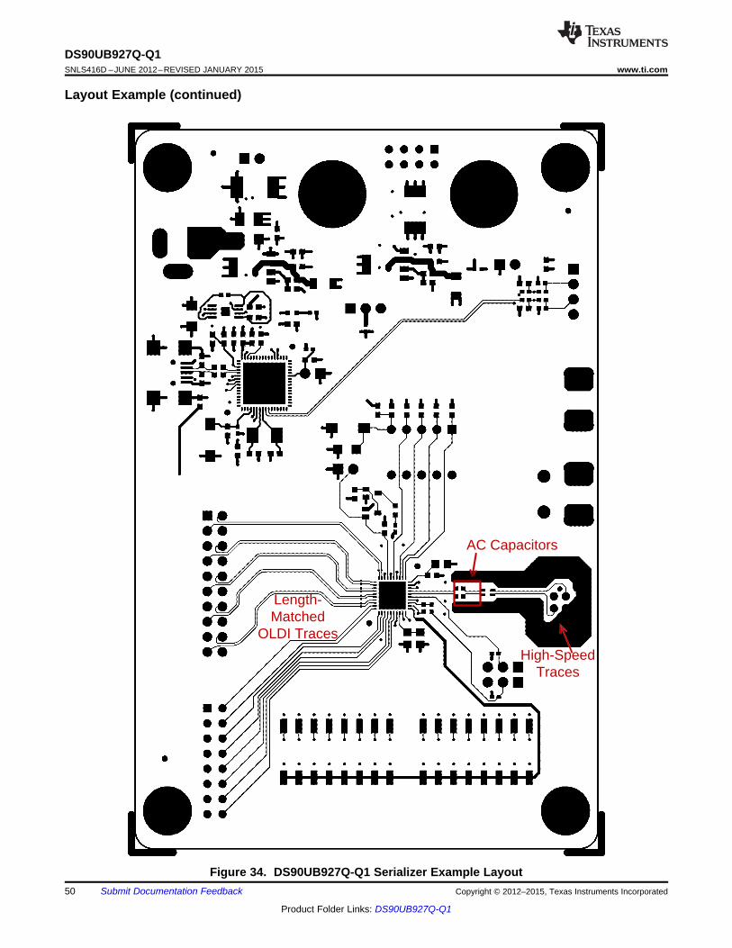
AC Capacitors
High-SpeedTraces
Length-Matched
OLDI Traces
DS90UB927Q-Q1SNLS416D –JUNE 2012–REVISED JANUARY 2015 www.ti.com
Layout Example (continued)
Figure 34. DS90UB927Q-Q1 Serializer Example Layout50 Submit Documentation Feedback Copyright © 2012–2015, Texas Instruments Incorporated
Product Folder Links: DS90UB927Q-Q1
DS90UB927Q-Q1www.ti.com SNLS416D –JUNE 2012–REVISED JANUARY 2015
11 Device and Documentation Support
11.1 Documentation Support
11.1.1 Related DocumentationFor related documentation see the following:• AN-2198 Exploring the Internal Test Pattern Generation Feature of 720p, SNLA132• I2C Communication Over FPD-Link III with Bidirectional Control Channel, SNLA131• AN-1187 Leadless Leadframe Package (LLP), SNOA401• AN-1108 Channel-Link PCB and Interconnect Design-In Guidelines, SNLA008• AN-905 Transmission Line RAPIDESIGNER Operation and Applications Guide, SNLA035• LVDS Owner’s Manual, SNLA187• QFN/SON PCB Attachment, SLUA271
11.2 TrademarksAll trademarks are the property of their respective owners.
11.3 Electrostatic Discharge CautionThese devices have limited built-in ESD protection. The leads should be shorted together or the device placed in conductive foamduring storage or handling to prevent electrostatic damage to the MOS gates.
11.4 GlossarySLYZ022 — TI Glossary.
This glossary lists and explains terms, acronyms, and definitions.
12 Mechanical, Packaging, and Orderable InformationThe following pages include mechanical, packaging, and orderable information. This information is the mostcurrent data available for the designated devices. This data is subject to change without notice and revision ofthis document. For browser-based versions of this data sheet, refer to the left-hand navigation.
Copyright © 2012–2015, Texas Instruments Incorporated Submit Documentation Feedback 51
Product Folder Links: DS90UB927Q-Q1
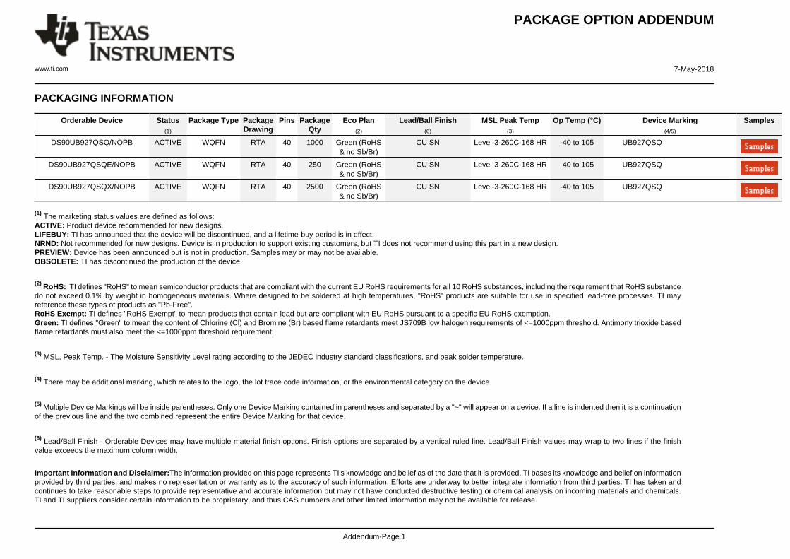
PACKAGE OPTION ADDENDUM
www.ti.com 7-May-2018
Addendum-Page 1
PACKAGING INFORMATION
Orderable Device Status(1)
Package Type PackageDrawing
Pins PackageQty
Eco Plan(2)
Lead/Ball Finish(6)
MSL Peak Temp(3)
Op Temp (°C) Device Marking(4/5)
Samples
DS90UB927QSQ/NOPB ACTIVE WQFN RTA 40 1000 Green (RoHS& no Sb/Br)
CU SN Level-3-260C-168 HR -40 to 105 UB927QSQ
DS90UB927QSQE/NOPB ACTIVE WQFN RTA 40 250 Green (RoHS& no Sb/Br)
CU SN Level-3-260C-168 HR -40 to 105 UB927QSQ
DS90UB927QSQX/NOPB ACTIVE WQFN RTA 40 2500 Green (RoHS& no Sb/Br)
CU SN Level-3-260C-168 HR -40 to 105 UB927QSQ
(1) The marketing status values are defined as follows:ACTIVE: Product device recommended for new designs.LIFEBUY: TI has announced that the device will be discontinued, and a lifetime-buy period is in effect.NRND: Not recommended for new designs. Device is in production to support existing customers, but TI does not recommend using this part in a new design.PREVIEW: Device has been announced but is not in production. Samples may or may not be available.OBSOLETE: TI has discontinued the production of the device.
(2) RoHS: TI defines "RoHS" to mean semiconductor products that are compliant with the current EU RoHS requirements for all 10 RoHS substances, including the requirement that RoHS substancedo not exceed 0.1% by weight in homogeneous materials. Where designed to be soldered at high temperatures, "RoHS" products are suitable for use in specified lead-free processes. TI mayreference these types of products as "Pb-Free".RoHS Exempt: TI defines "RoHS Exempt" to mean products that contain lead but are compliant with EU RoHS pursuant to a specific EU RoHS exemption.Green: TI defines "Green" to mean the content of Chlorine (Cl) and Bromine (Br) based flame retardants meet JS709B low halogen requirements of <=1000ppm threshold. Antimony trioxide basedflame retardants must also meet the <=1000ppm threshold requirement.
(3) MSL, Peak Temp. - The Moisture Sensitivity Level rating according to the JEDEC industry standard classifications, and peak solder temperature.
(4) There may be additional marking, which relates to the logo, the lot trace code information, or the environmental category on the device.
(5) Multiple Device Markings will be inside parentheses. Only one Device Marking contained in parentheses and separated by a "~" will appear on a device. If a line is indented then it is a continuationof the previous line and the two combined represent the entire Device Marking for that device.
(6) Lead/Ball Finish - Orderable Devices may have multiple material finish options. Finish options are separated by a vertical ruled line. Lead/Ball Finish values may wrap to two lines if the finishvalue exceeds the maximum column width.
Important Information and Disclaimer:The information provided on this page represents TI's knowledge and belief as of the date that it is provided. TI bases its knowledge and belief on informationprovided by third parties, and makes no representation or warranty as to the accuracy of such information. Efforts are underway to better integrate information from third parties. TI has taken andcontinues to take reasonable steps to provide representative and accurate information but may not have conducted destructive testing or chemical analysis on incoming materials and chemicals.TI and TI suppliers consider certain information to be proprietary, and thus CAS numbers and other limited information may not be available for release.
PACKAGE OPTION ADDENDUM
www.ti.com 7-May-2018
Addendum-Page 2
In no event shall TI's liability arising out of such information exceed the total purchase price of the TI part(s) at issue in this document sold by TI to Customer on an annual basis.
TAPE AND REEL INFORMATION
*All dimensions are nominal
Device PackageType
PackageDrawing
Pins SPQ ReelDiameter
(mm)
ReelWidth
W1 (mm)
A0(mm)
B0(mm)
K0(mm)
P1(mm)
W(mm)
Pin1Quadrant
DS90UB927QSQ/NOPB WQFN RTA 40 1000 330.0 16.4 6.3 6.3 1.5 12.0 16.0 Q1
DS90UB927QSQE/NOPB WQFN RTA 40 250 178.0 16.4 6.3 6.3 1.5 12.0 16.0 Q1
DS90UB927QSQX/NOPB WQFN RTA 40 2500 330.0 16.4 6.3 6.3 1.5 12.0 16.0 Q1
PACKAGE MATERIALS INFORMATION
www.ti.com 20-Sep-2016
Pack Materials-Page 1
*All dimensions are nominal
Device Package Type Package Drawing Pins SPQ Length (mm) Width (mm) Height (mm)
DS90UB927QSQ/NOPB WQFN RTA 40 1000 367.0 367.0 38.0
DS90UB927QSQE/NOPB WQFN RTA 40 250 210.0 185.0 35.0
DS90UB927QSQX/NOPB WQFN RTA 40 2500 367.0 367.0 38.0
PACKAGE MATERIALS INFORMATION
www.ti.com 20-Sep-2016
Pack Materials-Page 2
www.ti.com
PACKAGE OUTLINE
C
SEE TERMINALDETAIL
40X 0.30.2
4.6 0.1
40X 0.50.3
0.8 MAX
(0.1) TYP
0.050.00
36X 0.5
4X4.5
A 6.15.9
B
6.15.9
0.50.30.3
0.2
(0.2) TYP
WQFN - 0.8 mm max heightRTA0040APLASTIC QUAD FLATPACK - NO LEAD
4214989/B 02/2017
PIN 1 INDEX AREA
0.08SEATING PLANE
1
10 21
30
11 20
40 31
(OPTIONAL)PIN 1 ID
0.1 C A B0.05
EXPOSEDTHERMAL PAD
NOTES: 1. All linear dimensions are in millimeters. Any dimensions in parenthesis are for reference only. Dimensioning and tolerancing per ASME Y14.5M. 2. This drawing is subject to change without notice. 3. The package thermal pad must be soldered to the printed circuit board for thermal and mechanical performance.
SCALE 2.200
DETAILOPTIONAL TERMINAL
TYPICAL
www.ti.com
EXAMPLE BOARD LAYOUT
0.07 MINALL AROUND
0.07 MAXALL AROUND
40X (0.25)
40X (0.6)
( 0.2) TYPVIA
36X (0.5)
(5.8)
(5.8)
( 4.6)
(R0.05) TYP
(0.74)TYP
(1.31)TYP
(0.74) TYP(1.31 TYP)
WQFN - 0.8 mm max heightRTA0040APLASTIC QUAD FLATPACK - NO LEAD
4214989/B 02/2017
SYMM
1
10
11 20
21
30
3140
SYMM
LAND PATTERN EXAMPLEEXPOSED METAL SHOWN
SCALE:12X
NOTES: (continued) 4. This package is designed to be soldered to a thermal pad on the board. For more information, see Texas Instruments literature number SLUA271 (www.ti.com/lit/slua271).5. Vias are optional depending on application, refer to device data sheet. If any vias are implemented, refer to their locations shown on this view. It is recommended that vias under paste be filled, plugged or tented.
SOLDER MASKOPENING
METAL UNDERSOLDER MASK
SOLDER MASKDEFINED
EXPOSED METALMETAL
SOLDER MASKOPENING
SOLDER MASK DETAILS
NON SOLDER MASKDEFINED
(PREFERRED)
EXPOSED METAL
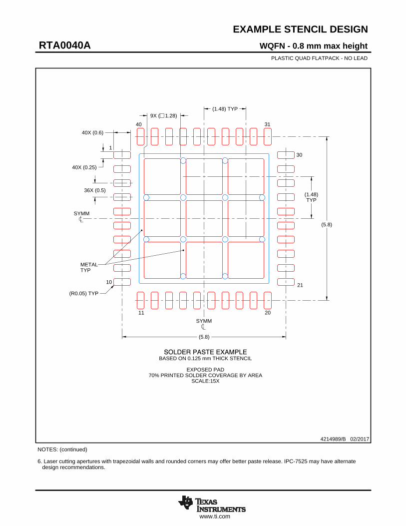
www.ti.com
EXAMPLE STENCIL DESIGN
40X (0.6)
40X (0.25)
36X (0.5)
(5.8)
(5.8)
9X ( 1.28)
(1.48)TYP
(R0.05) TYP
(1.48) TYP
WQFN - 0.8 mm max heightRTA0040APLASTIC QUAD FLATPACK - NO LEAD
4214989/B 02/2017
NOTES: (continued) 6. Laser cutting apertures with trapezoidal walls and rounded corners may offer better paste release. IPC-7525 may have alternate design recommendations.
SYMM
METALTYP
SOLDER PASTE EXAMPLEBASED ON 0.125 mm THICK STENCIL
EXPOSED PAD
70% PRINTED SOLDER COVERAGE BY AREASCALE:15X
SYMM
1
10
11 20
21
30
3140
IMPORTANT NOTICE
Texas Instruments Incorporated (TI) reserves the right to make corrections, enhancements, improvements and other changes to itssemiconductor products and services per JESD46, latest issue, and to discontinue any product or service per JESD48, latest issue. Buyersshould obtain the latest relevant information before placing orders and should verify that such information is current and complete.TI’s published terms of sale for semiconductor products (http://www.ti.com/sc/docs/stdterms.htm) apply to the sale of packaged integratedcircuit products that TI has qualified and released to market. Additional terms may apply to the use or sale of other types of TI products andservices.Reproduction of significant portions of TI information in TI data sheets is permissible only if reproduction is without alteration and isaccompanied by all associated warranties, conditions, limitations, and notices. TI is not responsible or liable for such reproduceddocumentation. Information of third parties may be subject to additional restrictions. Resale of TI products or services with statementsdifferent from or beyond the parameters stated by TI for that product or service voids all express and any implied warranties for theassociated TI product or service and is an unfair and deceptive business practice. TI is not responsible or liable for any such statements.Buyers and others who are developing systems that incorporate TI products (collectively, “Designers”) understand and agree that Designersremain responsible for using their independent analysis, evaluation and judgment in designing their applications and that Designers havefull and exclusive responsibility to assure the safety of Designers' applications and compliance of their applications (and of all TI productsused in or for Designers’ applications) with all applicable regulations, laws and other applicable requirements. Designer represents that, withrespect to their applications, Designer has all the necessary expertise to create and implement safeguards that (1) anticipate dangerousconsequences of failures, (2) monitor failures and their consequences, and (3) lessen the likelihood of failures that might cause harm andtake appropriate actions. Designer agrees that prior to using or distributing any applications that include TI products, Designer willthoroughly test such applications and the functionality of such TI products as used in such applications.TI’s provision of technical, application or other design advice, quality characterization, reliability data or other services or information,including, but not limited to, reference designs and materials relating to evaluation modules, (collectively, “TI Resources”) are intended toassist designers who are developing applications that incorporate TI products; by downloading, accessing or using TI Resources in anyway, Designer (individually or, if Designer is acting on behalf of a company, Designer’s company) agrees to use any particular TI Resourcesolely for this purpose and subject to the terms of this Notice.TI’s provision of TI Resources does not expand or otherwise alter TI’s applicable published warranties or warranty disclaimers for TIproducts, and no additional obligations or liabilities arise from TI providing such TI Resources. TI reserves the right to make corrections,enhancements, improvements and other changes to its TI Resources. TI has not conducted any testing other than that specificallydescribed in the published documentation for a particular TI Resource.Designer is authorized to use, copy and modify any individual TI Resource only in connection with the development of applications thatinclude the TI product(s) identified in such TI Resource. NO OTHER LICENSE, EXPRESS OR IMPLIED, BY ESTOPPEL OR OTHERWISETO ANY OTHER TI INTELLECTUAL PROPERTY RIGHT, AND NO LICENSE TO ANY TECHNOLOGY OR INTELLECTUAL PROPERTYRIGHT OF TI OR ANY THIRD PARTY IS GRANTED HEREIN, including but not limited to any patent right, copyright, mask work right, orother intellectual property right relating to any combination, machine, or process in which TI products or services are used. Informationregarding or referencing third-party products or services does not constitute a license to use such products or services, or a warranty orendorsement thereof. Use of TI Resources may require a license from a third party under the patents or other intellectual property of thethird party, or a license from TI under the patents or other intellectual property of TI.TI RESOURCES ARE PROVIDED “AS IS” AND WITH ALL FAULTS. TI DISCLAIMS ALL OTHER WARRANTIES ORREPRESENTATIONS, EXPRESS OR IMPLIED, REGARDING RESOURCES OR USE THEREOF, INCLUDING BUT NOT LIMITED TOACCURACY OR COMPLETENESS, TITLE, ANY EPIDEMIC FAILURE WARRANTY AND ANY IMPLIED WARRANTIES OFMERCHANTABILITY, FITNESS FOR A PARTICULAR PURPOSE, AND NON-INFRINGEMENT OF ANY THIRD PARTY INTELLECTUALPROPERTY RIGHTS. TI SHALL NOT BE LIABLE FOR AND SHALL NOT DEFEND OR INDEMNIFY DESIGNER AGAINST ANY CLAIM,INCLUDING BUT NOT LIMITED TO ANY INFRINGEMENT CLAIM THAT RELATES TO OR IS BASED ON ANY COMBINATION OFPRODUCTS EVEN IF DESCRIBED IN TI RESOURCES OR OTHERWISE. IN NO EVENT SHALL TI BE LIABLE FOR ANY ACTUAL,DIRECT, SPECIAL, COLLATERAL, INDIRECT, PUNITIVE, INCIDENTAL, CONSEQUENTIAL OR EXEMPLARY DAMAGES INCONNECTION WITH OR ARISING OUT OF TI RESOURCES OR USE THEREOF, AND REGARDLESS OF WHETHER TI HAS BEENADVISED OF THE POSSIBILITY OF SUCH DAMAGES.Unless TI has explicitly designated an individual product as meeting the requirements of a particular industry standard (e.g., ISO/TS 16949and ISO 26262), TI is not responsible for any failure to meet such industry standard requirements.Where TI specifically promotes products as facilitating functional safety or as compliant with industry functional safety standards, suchproducts are intended to help enable customers to design and create their own applications that meet applicable functional safety standardsand requirements. Using products in an application does not by itself establish any safety features in the application. Designers mustensure compliance with safety-related requirements and standards applicable to their applications. Designer may not use any TI products inlife-critical medical equipment unless authorized officers of the parties have executed a special contract specifically governing such use.Life-critical medical equipment is medical equipment where failure of such equipment would cause serious bodily injury or death (e.g., lifesupport, pacemakers, defibrillators, heart pumps, neurostimulators, and implantables). Such equipment includes, without limitation, allmedical devices identified by the U.S. Food and Drug Administration as Class III devices and equivalent classifications outside the U.S.TI may expressly designate certain products as completing a particular qualification (e.g., Q100, Military Grade, or Enhanced Product).Designers agree that it has the necessary expertise to select the product with the appropriate qualification designation for their applicationsand that proper product selection is at Designers’ own risk. Designers are solely responsible for compliance with all legal and regulatoryrequirements in connection with such selection.Designer will fully indemnify TI and its representatives against any damages, costs, losses, and/or liabilities arising out of Designer’s non-compliance with the terms and provisions of this Notice.
Mailing Address: Texas Instruments, Post Office Box 655303, Dallas, Texas 75265Copyright © 2018, Texas Instruments Incorporated


![DS90UB925Q-Q1 5 to 85 MHz 24-Bit Color FPD-Link III ... · R[7:0] HS VS PCLK PDB Serializer Deserializer DE RGB Display 720p RGB Digital Display Interface 24-bit color depth HOST](https://img.pdfslide.net/doc/110x75/5b15b9467f8b9ac7128e0767/ds90ub925q-q1-5-to-85-mhz-24-bit-color-fpd-link-iii-r70-hs-vs-pclk-pdb.jpg)


![DS90UR90xQ-Q1 5- to 65-MHz, 24-bit Color FPD-Link II ...7:0] HS VS PCLK PDB Serializer Deserializer DE RGB Display QVGAto XGA RGB Digital Display Interface 24-bit color depth HOST](https://img.pdfslide.net/doc/110x75/5b47aff07f8b9a501f8cfc25/ds90ur90xq-q1-5-to-65-mhz-24-bit-color-fpd-link-ii-70-hs-vs-pclk-pdb-serializer.jpg)