Embed Size (px)
Citation preview
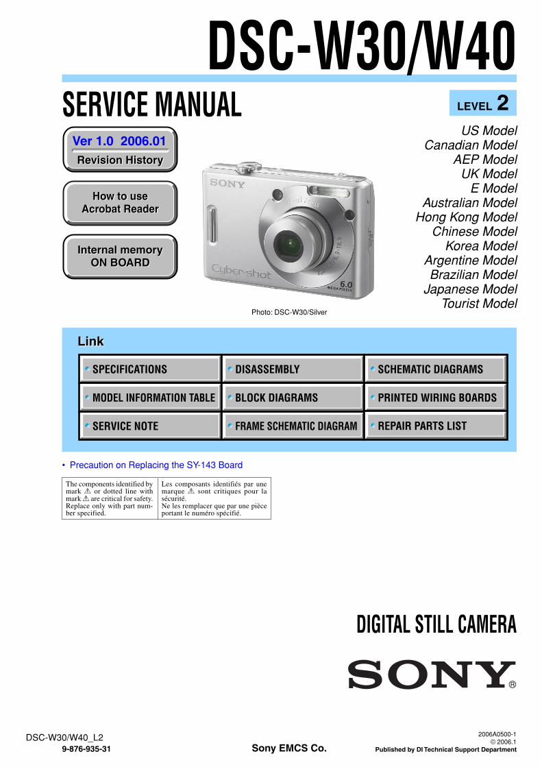
SERVICE MANUAL LEVEL 2
LinkLink
Revision HistoryRevision History
How to useAcrobat Reader
How to useAcrobat Reader
Sony EMCS Co.DSC-W30/W40_L2
Internal memoryON BOARD
Internal memoryON BOARD
SERVICE NOTE
MODEL INFORMATION TABLE
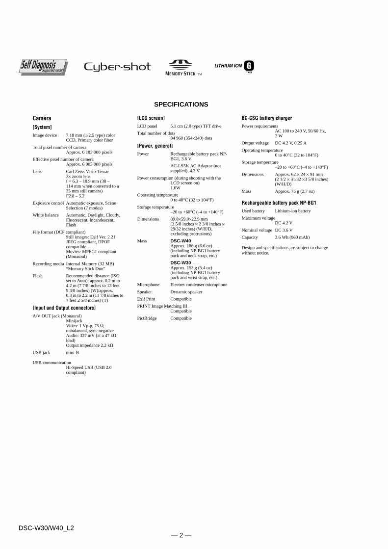
SPECIFICATIONS
FRAME SCHEMATIC DIAGRAM
BLOCK DIAGRAMS
DISASSEMBLY
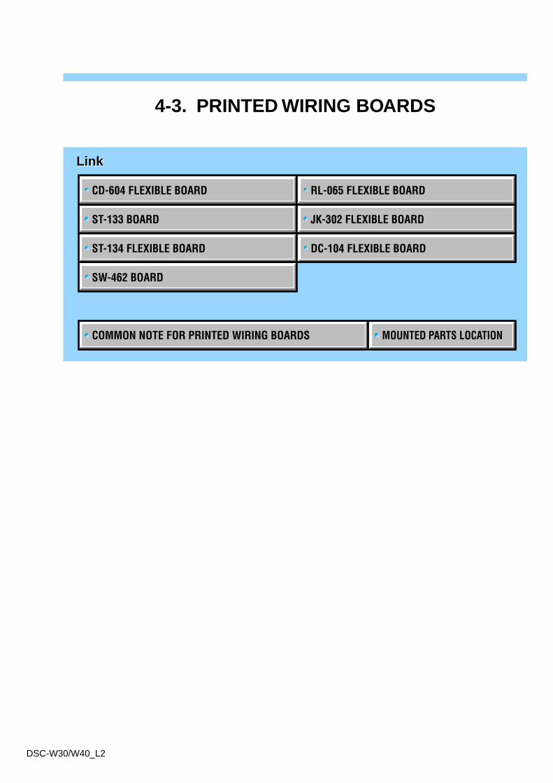
PRINTED WIRING BOARDS
REPAIR PARTS LIST
SCHEMATIC DIAGRAMS
Ver 1.0 2006.01
DIGITAL STILL CAMERA
2006A0500-1 © 2006.1
Published by DI Technical Support Department9-876-935-31
US ModelCanadian Model
AEP ModelUK Model
E ModelAustralian Model
Hong Kong ModelChinese Model
Korea ModelArgentine ModelBrazilian Model
Japanese ModelTourist Model
The components identified bymark 0 or dotted line withmark 0 are critical for safety.Replace only with part num-ber specified.
Les composants identifiés par unemarque 0 sont critiques pour lasécurité.Ne les remplacer que par une pièceportant le numéro spécifié.
• Precaution on Replacing the SY-143 Board
DSC-W30/W40
Photo: DSC-W30/Silver
— 2 —DSC-W30/W40_L2
SPECIFICATIONS
Camera[System]Image device 7.18 mm (1/2.5 type) color
CCD, Primary color filter
Total pixel number of cameraApprox. 6 183 000 pixels
Effective pixel number of cameraApprox. 6 003 000 pixels
Lens Carl Zeiss Vario-Tessar3× zoom lensf = 6.3 – 18.9 mm (38 – 114 mm when converted to a 35 mm still camera)F2.8 – 5.2
Exposure control Automatic exposure, Scene Selection (7 modes)
White balance Automatic, Daylight, Cloudy, Fluorescent, Incandescent, Flash
File format (DCF compliant)Still images: Exif Ver. 2.21JPEG compliant, DPOF compatibleMovies: MPEG1 compliant (Monaural)
Recording media Internal Memory (32 MB)“Memory Stick Duo”
Flash Recommended distance (ISO set to Auto): approx. 0.2 m to 4.2 m (7 7/8 inches to 13 feet 9 3/8 inches) (W)/approx. 0.3 m to 2.2 m (11 7/8 inches to 7 feet 2 5/8 inches) (T)
[Input and Output connectors]A/V OUT jack (Monaural)
MinijackVideo: 1 Vp-p, 75 Ω,unbalanced, sync negativeAudio: 327 mV (at a 47 kΩ load)Output impedance 2.2 kΩ
USB jack mini-B
USB communicationHi-Speed USB (USB 2.0 compliant)
[LCD screen]LCD panel 5.1 cm (2.0 type) TFT drive
Total number of dots84 960 (354×240) dots
[Power, general]Power Rechargeable battery pack NP-
BG1, 3.6 V
AC-LS5K AC Adaptor (not supplied), 4.2 V
Power consumption (during shooting with the LCD screen on)1.0W
Operating temperature0 to 40°C (32 to 104°F)
Storage temperature–20 to +60°C (–4 to +140°F)
Dimensions 89.8×59.0×22.9 mm(3 5/8 inches × 2 3/8 inches × 29/32 inches) (W/H/D, excluding protrusions)
Mass DSC-W40Approx. 186 g (6.6 oz) (including NP-BG1 battery pack and neck strap, etc.)
DSC-W30Approx. 153 g (5.4 oz) (including NP-BG1 battery pack and wrist strap, etc.)
Microphone Electret condenser microphone
Speaker Dynamic speaker
Exif Print Compatible
PRINT Image Matching IIICompatible
PictBridge Compatible
BC-CSG battery chargerPower requirements
AC 100 to 240 V, 50/60 Hz, 2 W
Output voltage DC 4.2 V, 0.25 A
Operating temperature0 to 40°C (32 to 104°F)
Storage temperature–20 to +60°C (–4 to +140°F)
Dimensions Approx. 62 × 24 × 91 mm(2 1/2 × 31/32 ×3 5/8 inches) (W/H/D)
Mass Approx. 75 g (2.7 oz)
Rechargeable battery pack NP-BG1Used battery Lithium-ion battery
Maximum voltageDC 4.2 V
Nominal voltage DC 3.6 V
Capacity 3.6 Wh (960 mAh)
Design and specifications are subject to change without notice.
— 3 —DSC-W30/W40_L2
SAFETY-RELATED COMPONENT WARNING!!
COMPONENTS IDENTIFIED BY MARK 0 OR DOTTED LINE WITHMARK 0 ON THE SCHEMATIC DIAGRAMS AND IN THE PARTSLIST ARE CRITICAL TO SAFE OPERATION. REPLACE THESECOMPONENTS WITH SONY PARTS WHOSE PART NUMBERSAPPEAR AS SHOWN IN THIS MANUAL OR IN SUPPLEMENTSPUBLISHED BY SONY.
ATTENTION AU COMPOSANT AYANT RAPPORTÀ LA SÉCURITÉ!
LES COMPOSANTS IDENTIFÉS PAR UNE MARQUE 0 SUR LESDIAGRAMMES SCHÉMATIQUES ET LA LISTE DES PIÈCES SONTCRITIQUES POUR LA SÉCURITÉ DE FONCTIONNEMENT. NEREMPLACER CES COMPOSANTS QUE PAR DES PIÈSES SONYDONT LES NUMÉROS SONT DONNÉS DANS CE MANUEL OUDANS LES SUPPÉMENTS PUBLIÉS PAR SONY.
1. Check the area of your repair for unsoldered or poorly-solderedconnections. Check the entire board surface for solder splashesand bridges.
2. Check the interboard wiring to ensure that no wires are"pinched" or contact high-wattage resistors.
3. Look for unauthorized replacement parts, particularlytransistors, that were installed during a previous repair. Pointthem out to the customer and recommend their replacement.
4. Look for parts which, through functioning, show obvious signsof deterioration. Point them out to the customer andrecommend their replacement.
5. Check the B+ voltage to see it is at the values specified.6. FLEXIBLE Circuit Board Repairing
• Keep the temperature of the soldering iron around 270°Cduring repairing.
• Do not touch the soldering iron on the same conductor of thecircuit board (within 3 times).
• Be careful not to apply force on the conductor when solderingor unsoldering.
Unleaded solderBoards requiring use of unleaded solder are printed with the lead-free mark (LF) indicating the solder contains no lead.(Caution: Some printed circuit boards may not come printed withthe lead free mark due to their particular size.)
: LEAD FREE MARKUnleaded solder has the following characteristics.• Unleaded solder melts at a temperature about 40°C higher than
ordinary solder.Ordinary soldering irons can be used but the iron tip has to beapplied to the solder joint for a slightly longer time.Soldering irons using a temperature regulator should be set toabout 350°C.Caution: The printed pattern (copper foil) may peel away if theheated tip is applied for too long, so be careful!
• Strong viscosityUnleaded solder is more viscous (sticky, less prone to flow) thanordinary solder so use caution not to let solder bridges occur suchas on IC pins, etc.
• Usable with ordinary solderIt is best to use only unleaded solder but unleaded solder mayalso be added to ordinary solder.
SAFETY CHECK-OUT
After correcting the original service problem, perform the following
safety checks before releasing the set to the customer.
CAUTIONDanger of explosion if battery is incorrectly replaced.Replace only with the same or equivalent type.
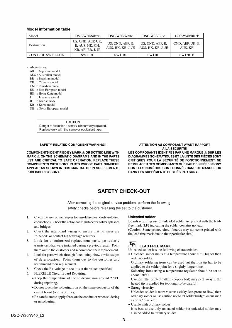
Model DSC-W30/Silver DSC-W30/White DSC-W30/Blue DSC-W40/Black
DestinationUS, CND, AEP, UK,
US, CND, AEP, E, US, CND, AEP, E, CND, AEP, UK, E,E, AUS, HK, CH,
AUS, HK, KR, J, JE AUS, HK, KR, J, JE AUS, KRKR, AR, BR, J, JE
CONTROL SW BLOCK SW110T SW110T SW110T SW120TB
Model information table
• AbbreviationAR : Argentine modelAUS : Australian modelBR : Brazilian modelCH : Chinese modelCND : Canadian modelEE : East European modelHK : Hong Kong modelJ : Japanese modelJE : Tourist modelKR : Korea modelNE : North European model
— 4 —DSC-W30/W40_L2
TABLE OF CONTENTS
1. SERVICE NOTE1-1. Description on Self-diagnosis Display ···························· 1-11-2. Process After Fixing Flash Error ····································· 1-11-3. Method for Copying or Erasing the Data in Internal
Memory ··········································································· 1-21-4. Precaution on Replacing the SY-143 Board ···················· 1-3
2. DISASSEMBLY2-1. Disassembly ····································································· 2-22-2. Exchange Method of Barrier Assy ·································· 2-62-3. Exchange Method of Zoom Motor Unit ·························· 2-9
3. BLOCK DIAGRAMS3-1. Overall Block Diagram (1/2) ··········································· 3-13-2. Overall Block Diagram (2/2) ··········································· 3-23-3. Power Block Diagram ····················································· 3-3
4. PRINTED WIRING BOARDS ANDSCHEMATIC DIAGRAMS
4-1. Frame Schematic Diagram ·············································· 4-14-2. Schematic Diagrams ························································ 4-34-3. Printed Wiring Boards ··················································· 4-174-4. Mounted Parts Location ················································ 4-26
5. REPAIR PARTS LIST5-1. Exploded Views ······························································· 5-25-2. Electrical Parts List ························································· 5-6
Section Title Page
1-1DSC-W30/W40_L2
1. SERVICE NOTE
Self-diagnosis display• C: ss: ss
You can reverse the cameramalfunction yourself. (However,contact your Sony dealer or localauthorized Sony service facilitywhen you cannot recover from thecamera malfunction.)
• E: ss: ssContact your Sony dealer or localauthorized Sony service facility.
Display Code
C:32:ss
C:13:ss
Countermeasure
Turn the power off and on again.
Format the “Memory Stick” or internalmemory.
Cause
Trouble with hardware.
“Memory Stick” or internal memory isunformatted.
Caution Display During Error
SYSTEM ERROR
FORMAT ERROR
MEMORY STICK ERROR
E:61:ss
E:91:ss
1-1. DESCRIPTION ON SELF-DIAGNOSIS DISPLAY
Insert a new “Memory Stick”. “Memory Stick” is broken.
Turn the power off and on again. Trouble with internal memory. INTERNAL MEMORY ERROR
Checking of lens drive circuit. When failed in the focus and zoominitialization. —
Checking of flash unit or replacementof flash unit. (Note)
Abnormality when flash is beingcharged.
Note: After repair, be sure to perfom “1-2. PROCESS AFTER FIXING FLASH ERROR”.
1-2. PROCESS AFTER FIXING FLASH ERROR
When “FLASH error” (Self-diagnosis Code E : 91 : ** ) occurs, to prevent any abnormal situation caused by high voltage, setting of theflash is changed automatically to disabling charge and flash setting.After fixing, this setting needs to be deactivated. Flash error code can be initialized by the operations on the Setup screen.
Method for Initializing the Flash Error Code
Initializes the setting to the default setting.
1 Select [OK] with v on the control button, then press z.The message “Initialize all settings Ready?” appears.
2 Select [OK] with v, then press z.The settings are reset to the default setting.
• Make sure that the power is not disconnected during resetting.
Initialize
OK See the following procedure.
Cancel Cancels the resetting.
1-2DSC-W30/W40_L2
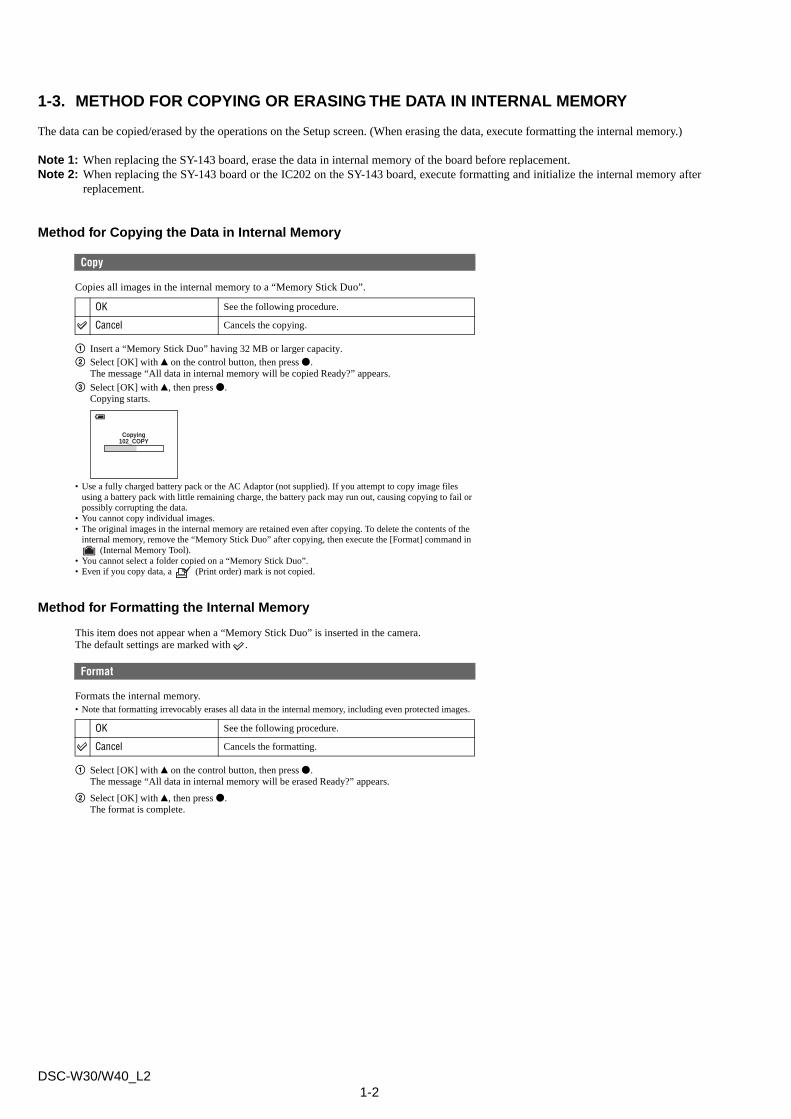
1-3. METHOD FOR COPYING OR ERASING THE DATA IN INTERNAL MEMORY
The data can be copied/erased by the operations on the Setup screen. (When erasing the data, execute formatting the internal memory.)
Note 1: When replacing the SY-143 board, erase the data in internal memory of the board before replacement.Note 2: When replacing the SY-143 board or the IC202 on the SY-143 board, execute formatting and initialize the internal memory after
replacement.
Method for Copying the Data in Internal Memory
Method for Formatting the Internal Memory
Copies all images in the internal memory to a “Memory Stick Duo”.
1 Insert a “Memory Stick Duo” having 32 MB or larger capacity.2 Select [OK] with v on the control button, then press z.
The message “All data in internal memory will be copied Ready?” appears.
3 Select [OK] with v, then press z.Copying starts.
• Use a fully charged battery pack or the AC Adaptor (not supplied). If you attempt to copy image files using a battery pack with little remaining charge, the battery pack may run out, causing copying to fail or possibly corrupting the data.
• You cannot copy individual images.• The original images in the internal memory are retained even after copying. To delete the contents of the
internal memory, remove the “Memory Stick Duo” after copying, then execute the [Format] command in (Internal Memory Tool).
• You cannot select a folder copied on a “Memory Stick Duo”.• Even if you copy data, a (Print order) mark is not copied.
Copy
OK See the following procedure.
Cancel Cancels the copying.
Copying102_COPY
This item does not appear when a “Memory Stick Duo” is inserted in the camera.The default settings are marked with .
Formats the internal memory.• Note that formatting irrevocably erases all data in the internal memory, including even protected images.
1 Select [OK] with v on the control button, then press z.The message “All data in internal memory will be erased Ready?” appears.
2 Select [OK] with v, then press z.The format is complete.
Format
OK See the following procedure.
Cancel Cancels the formatting.
1-3DSC-W30/W40_L2
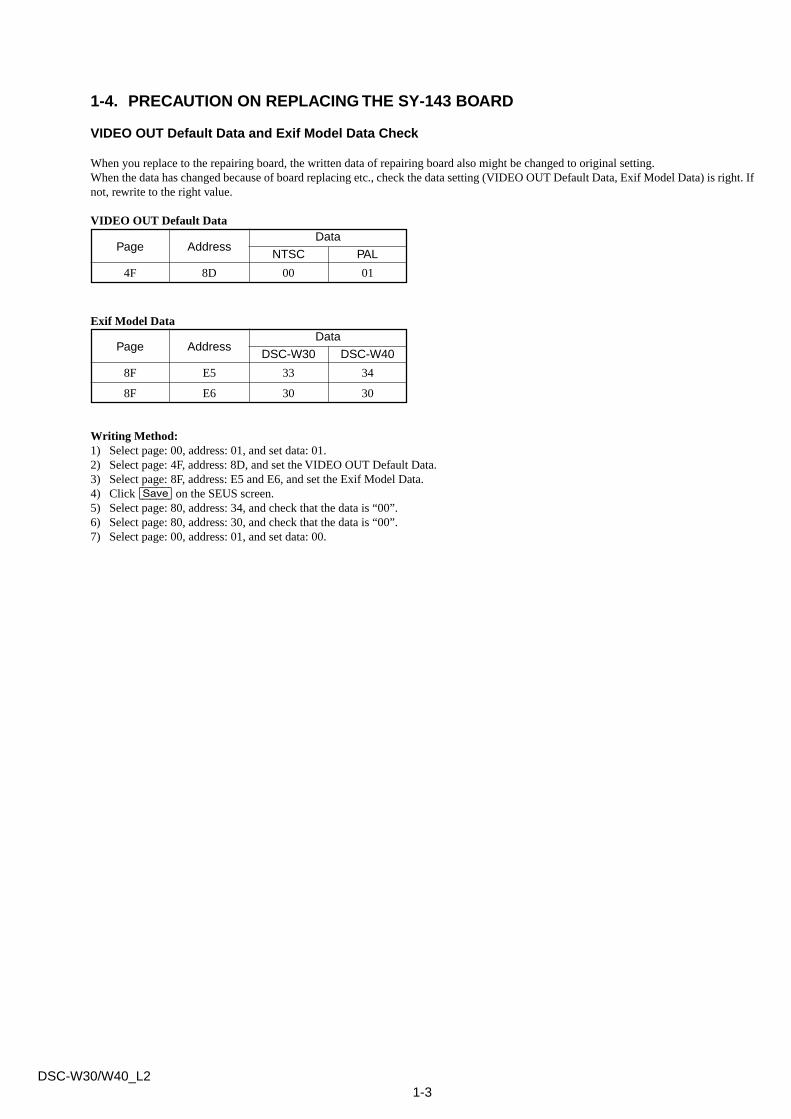
1-4. PRECAUTION ON REPLACING THE SY-143 BOARD
VIDEO OUT Default Data and Exif Model Data Check
When you replace to the repairing board, the written data of repairing board also might be changed to original setting.When the data has changed because of board replacing etc., check the data setting (VIDEO OUT Default Data, Exif Model Data) is right. Ifnot, rewrite to the right value.
VIDEO OUT Default Data
Exif Model Data
Writing Method:1) Select page: 00, address: 01, and set data: 01.2) Select page: 4F, address: 8D, and set the VIDEO OUT Default Data.3) Select page: 8F, address: E5 and E6, and set the Exif Model Data.4) Click [Save] on the SEUS screen.5) Select page: 80, address: 34, and check that the data is “00”.6) Select page: 80, address: 30, and check that the data is “00”.7) Select page: 00, address: 01, and set data: 00.
Address
33 34E58F
PageData
DSC-W30 DSC-W40
30 30E68F
Address
00 018D4F
PageData
NTSC PAL
1-4EDSC-W30/W40_L2
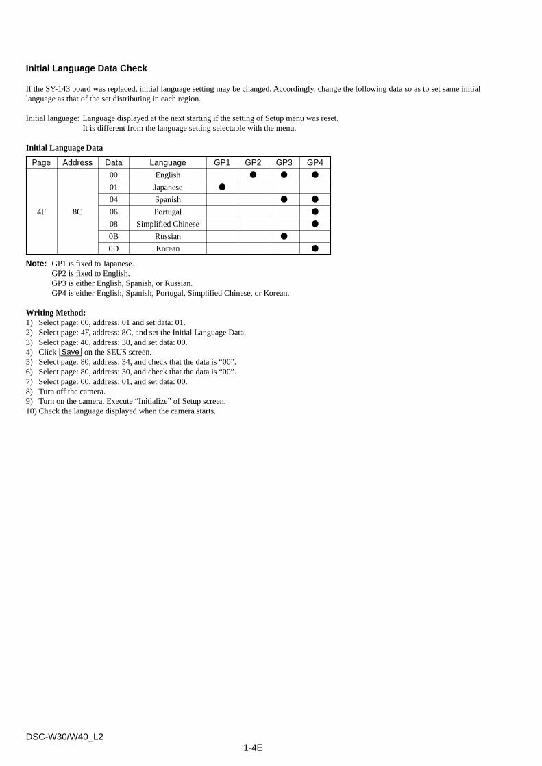
Initial Language Data Check
If the SY-143 board was replaced, initial language setting may be changed. Accordingly, change the following data so as to set same initiallanguage as that of the set distributing in each region.
Initial language: Language displayed at the next starting if the setting of Setup menu was reset.It is different from the language setting selectable with the menu.
Initial Language Data
Page Address Data Language GP1 GP2 GP3 GP4
4F 8C
00 English z z z
01 Japanese z
04 Spanish z z
06 Portugal z
08 Simplified Chinese z
0B Russian z
0D Korean z
Note: GP1 is fixed to Japanese.GP2 is fixed to English.GP3 is either English, Spanish, or Russian.GP4 is either English, Spanish, Portugal, Simplified Chinese, or Korean.
Writing Method:1) Select page: 00, address: 01 and set data: 01.2) Select page: 4F, address: 8C, and set the Initial Language Data.3) Select page: 40, address: 38, and set data: 00.4) Click [Save] on the SEUS screen.5) Select page: 80, address: 34, and check that the data is “00”.6) Select page: 80, address: 30, and check that the data is “00”.7) Select page: 00, address: 01, and set data: 00.8) Turn off the camera.9) Turn on the camera. Execute “Initialize” of Setup screen.10) Check the language displayed when the camera starts.
2-1
2. DISASSEMBLY
DSC-W30/W40_L2
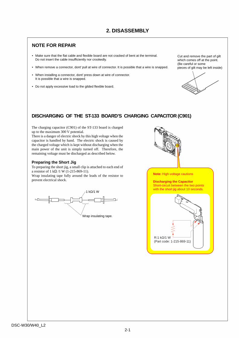
NOTE FOR REPAIR
• Make sure that the flat cable and flexible board are not cracked of bent at the terminal.Do not insert the cable insufficiently nor crookedly.
• When remove a connector, dont’ pull at wire of connector. It is possible that a wire is snapped.
• When installing a connector, dont’ press down at wire of connector.It is possible that a wire is snapped.
• Do not apply excessive load to the gilded flexible board.
Cut and remove the part of gilt which comes off at the point.(Be careful or some pieces of gilt may be left inside)
DISCHARGING OF THE ST-133 BOARD’S CHARGING CAPACITOR (C901)
The charging capacitor (C901) of the ST-133 board is chargedup to the maximum 300 V potential.There is a danger of electric shock by this high voltage when thecapacitor is handled by hand. The electric shock is caused bythe charged voltage which is kept without discharging when themain power of the unit is simply turned off. Therefore, theremaining voltage must be discharged as described below.
Preparing the Short JigTo preparing the short jig, a small clip is attached to each end ofa resistor of 1 kΩ /1 W (1-215-869-11).Wrap insulating tape fully around the leads of the resistor toprevent electrical shock.
1 kΩ/1 W
Wrap insulating tape.
Note: High-voltage cautions
Discharging the CapacitorShort-circuit between the two points with the short jig about 10 seconds.
R:1 kΩ/1 W (Part code: 1-215-869-11)
2-2DSC-W30/W40_L2
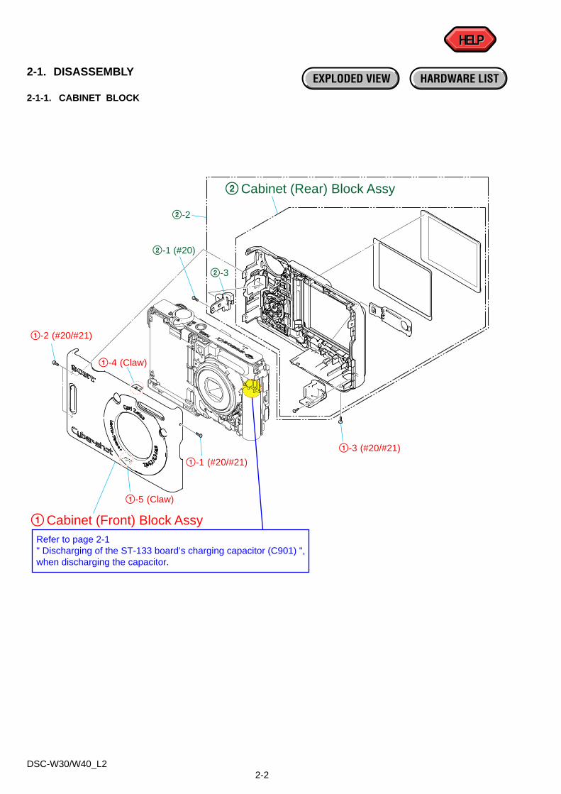
2-1. DISASSEMBLY
2-1-1. CABINET BLOCK
HELPHELP
2Cabinet (Rear) Block Assy
1Cabinet (Front) Block Assy
1-1 (#20/#21)
1-3 (#20/#21)
1-2 (#20/#21)
2-1 (#20)
2-3
2-2
Refer to page 2-1 " Discharging of the ST-133 board’s charging capacitor (C901) ", when discharging the capacitor.
1-5 (Claw)
1-4 (Claw)
EXPLODED VIEW HARDWARE LIST
2-3DSC-W30/W40_L2
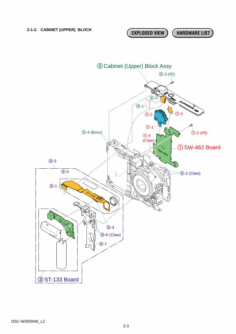
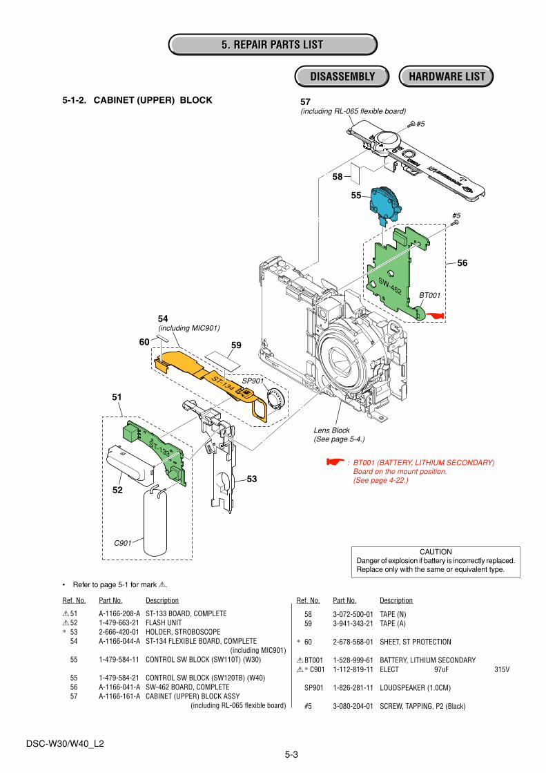
2-1-2. CABINET (UPPER) BLOCK
SW-462
2Cabinet (Upper) Block Assy
1SW-462 Board
1-3 (#5)1-4(Claw)
1-2
1-1
1-5
2-3 (#5)
2-2
2-1
2-4 (Boss)
3ST-133 Board
3-2 (Claw)
3-1
3-4
3-7
3-5
3-3
3-6 (Claw)
ST-133
ST-134
EXPLODED VIEW HARDWARE LIST
2-4DSC-W30/W40_L2
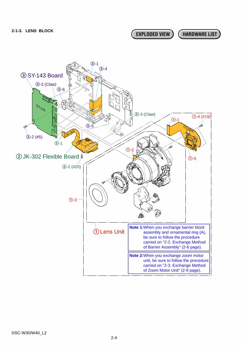
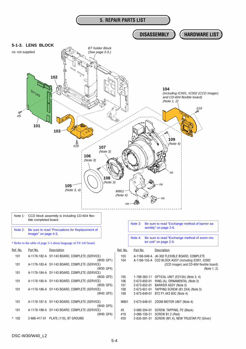
2-1-3. LENS BLOCK
1-4 (#19)1-1
1-2
1-5
1-3
1Lens Unit
CD-604
Note 1:When you exchange barrier block assembly and ornamental ring (A), be sure to follow the procedure carried on "2-2. Exchange Method of Barrier Assembly" (2-6 page).
Note 2:When you exchange zoom motor unit, be sure to follow the procedure carried on "2-3. Exchange Method of Zoom Motor Unit" (2-9 page).
2-2 (#20)
2-1
2 JK-302 Flexible Board
JK-302
SY-143
3-3 (Claw)
3SY-143 Board
2-3 (Claw)
3-2 (#5)
3-13-4
3-5
3-6
EXPLODED VIEW HARDWARE LIST
2-5DSC-W30/W40_L2
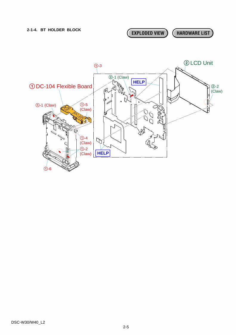
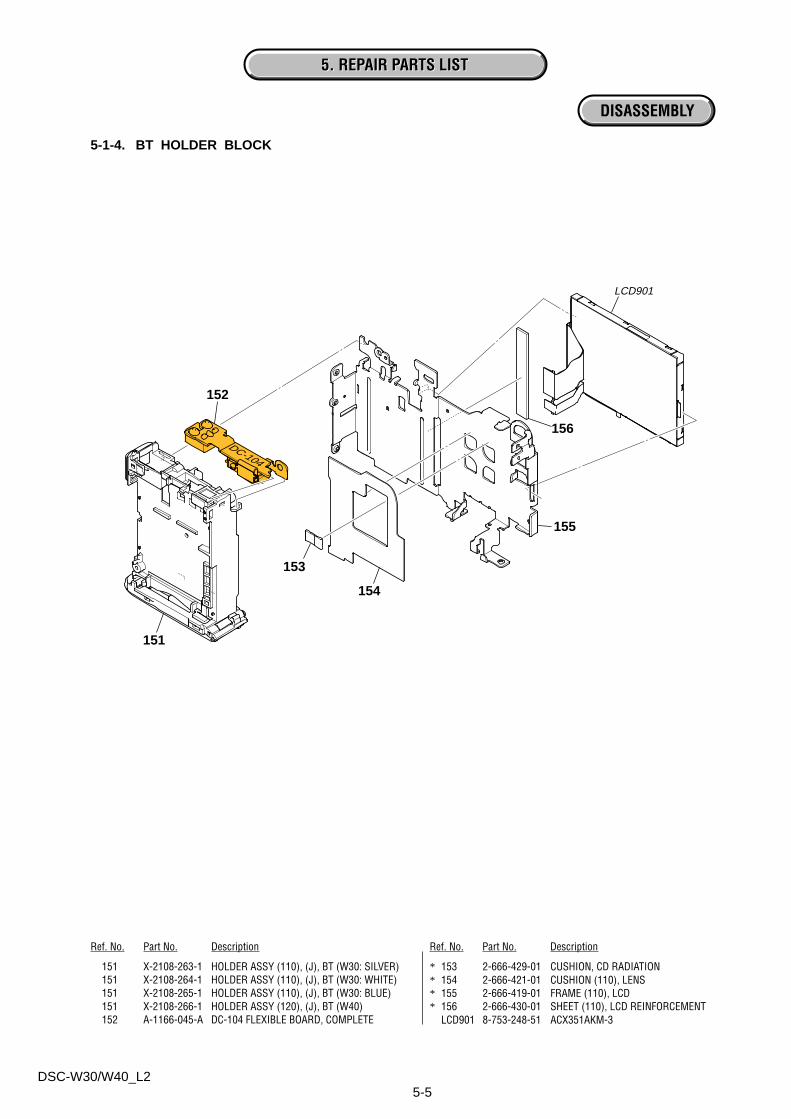
2-1-4. BT HOLDER BLOCK
1DC-104 Flexible Board
1-1 (Claw)
1-6
1-3
2-1 (Claw)
2-2(Claw)
1-2(Claw)
1-4(Claw)
1-5(Claw)
2LCD Unit
HELP
HELP
DC-104
EXPLODED VIEW HARDWARE LIST
2-6DSC-W30/W40_L2
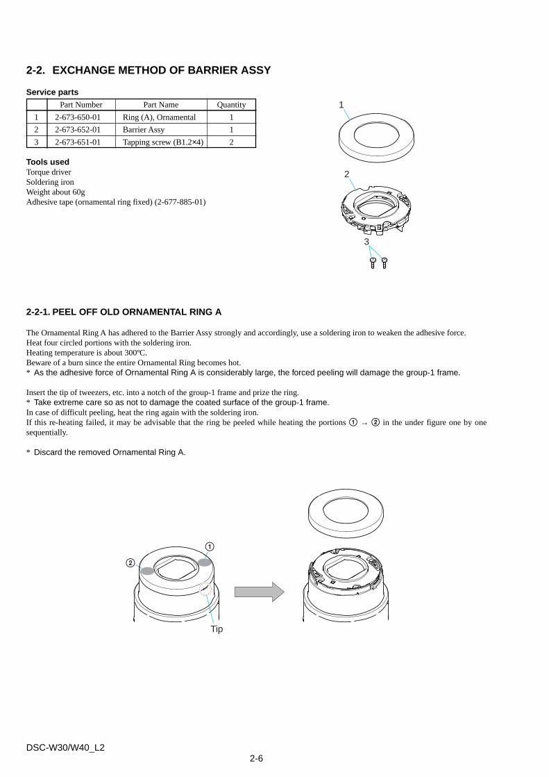
2-2. EXCHANGE METHOD OF BARRIER ASSY
Service parts
Part Number Part Name Quantity
1 2-673-650-01 Ring (A), Ornamental 1
2 2-673-652-01 Barrier Assy 1
3 2-673-651-01 Tapping screw (B1.2×4) 2
Tools usedTorque driverSoldering ironWeight about 60gAdhesive tape (ornamental ring fixed) (2-677-885-01)
2-2-1. PEEL OFF OLD ORNAMENTAL RING A
The Ornamental Ring A has adhered to the Barrier Assy strongly and accordingly, use a soldering iron to weaken the adhesive force.Heat four circled portions with the soldering iron.Heating temperature is about 300ºC.Beware of a burn since the entire Ornamental Ring becomes hot.* As the adhesive force of Ornamental Ring A is considerably large, the forced peeling will damage the group-1 frame.
Insert the tip of tweezers, etc. into a notch of the group-1 frame and prize the ring.* Take extreme care so as not to damage the coated surface of the group-1 frame.In case of difficult peeling, heat the ring again with the soldering iron.If this re-heating failed, it may be advisable that the ring be peeled while heating the portions 1 → 2 in the under figure one by onesequentially.
* Discard the removed Ornamental Ring A.
1
2
3
Tip
1
2
2-7DSC-W30/W40_L2
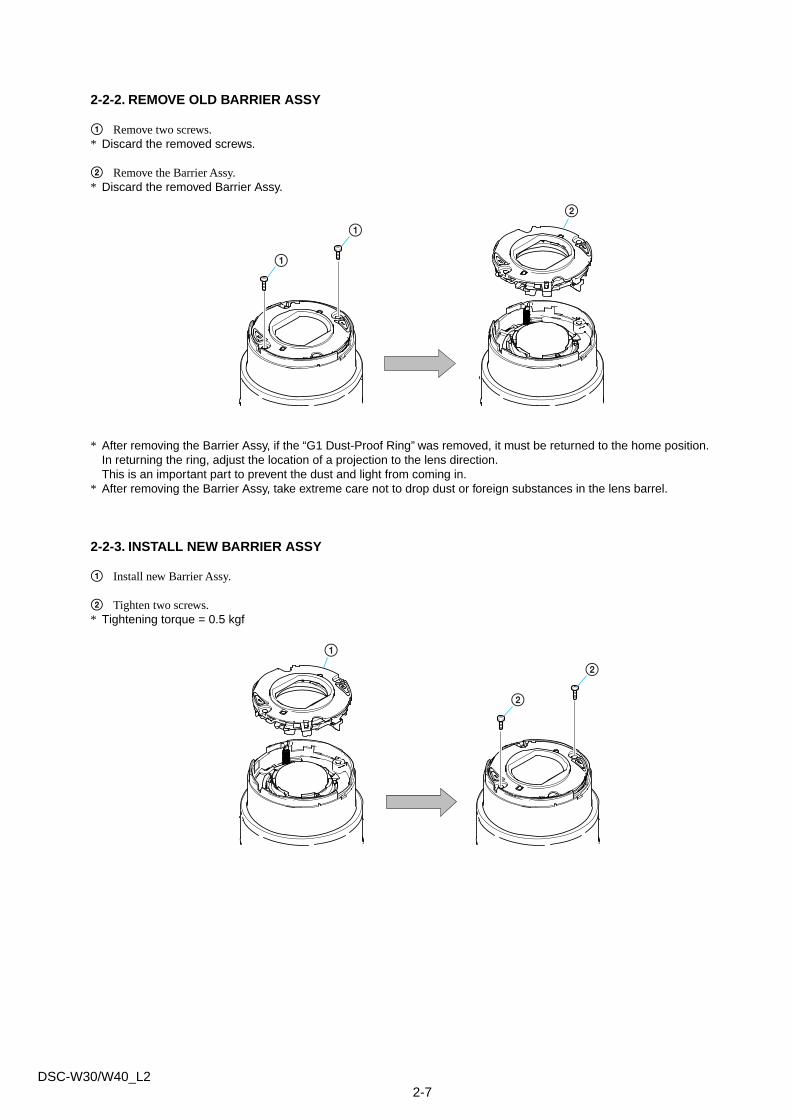
2-2-2. REMOVE OLD BARRIER ASSY
1 Remove two screws.* Discard the removed screws.
2 Remove the Barrier Assy.* Discard the removed Barrier Assy.
* After removing the Barrier Assy, if the “G1 Dust-Proof Ring” was removed, it must be returned to the home position.In returning the ring, adjust the location of a projection to the lens direction.This is an important part to prevent the dust and light from coming in.
* After removing the Barrier Assy, take extreme care not to drop dust or foreign substances in the lens barrel.
2-2-3. INSTALL NEW BARRIER ASSY
1 Install new Barrier Assy.
2 Tighten two screws.* Tightening torque = 0.5 kgf
1
1
2
2
2
1
2-8DSC-W30/W40_L2
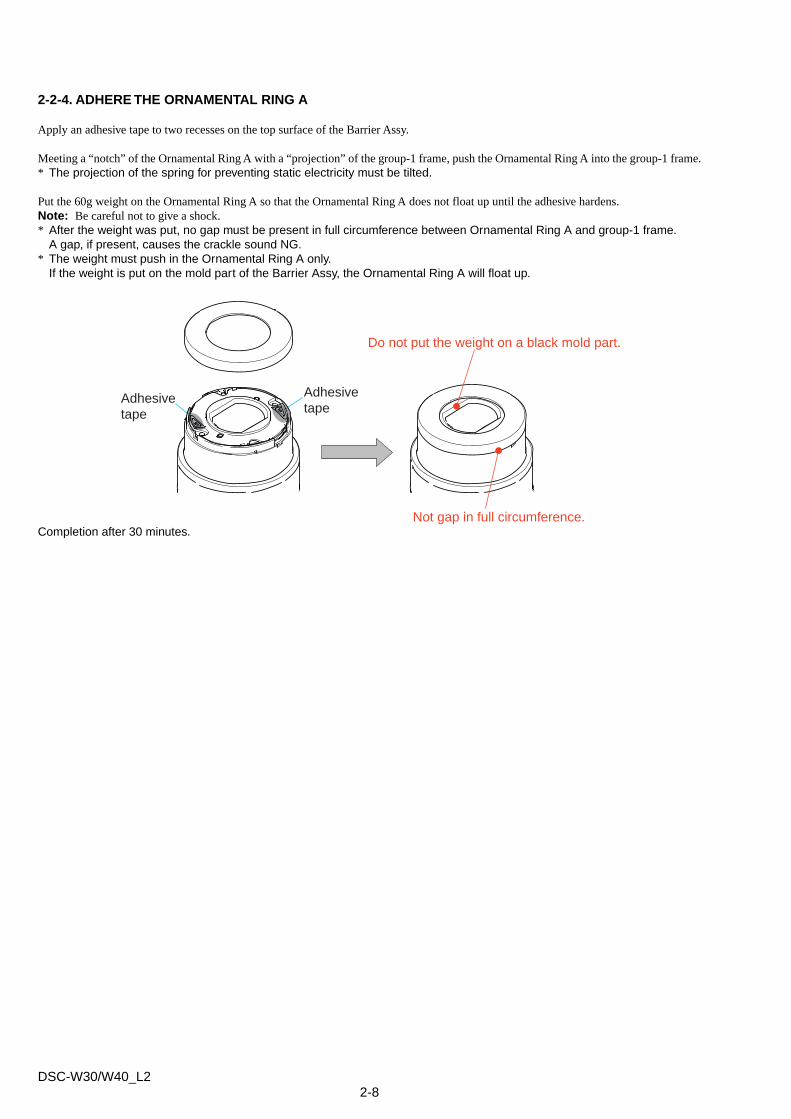
2-2-4. ADHERE THE ORNAMENTAL RING A
Apply an adhesive tape to two recesses on the top surface of the Barrier Assy.
Meeting a “notch” of the Ornamental Ring A with a “projection” of the group-1 frame, push the Ornamental Ring A into the group-1 frame.* The projection of the spring for preventing static electricity must be tilted.
Put the 60g weight on the Ornamental Ring A so that the Ornamental Ring A does not float up until the adhesive hardens.Note: Be careful not to give a shock.* After the weight was put, no gap must be present in full circumference between Ornamental Ring A and group-1 frame.
A gap, if present, causes the crackle sound NG.* The weight must push in the Ornamental Ring A only.
If the weight is put on the mold part of the Barrier Assy, the Ornamental Ring A will float up.
Completion after 30 minutes.
Adhesivetape
Adhesivetape
Do not put the weight on a black mold part.
Not gap in full circumference.
2-9EDSC-W30/W40_L2
2-3. EXCHANGE METHOD OF ZOOM MOTOR UNIT
Service parts
Part Number Part Name Quantity
1 2-673-648-01 Zoom Motor Unit 1
2 2-673-649-01 BT2 P1.4×3 B3C 2
Tools usedTorque driver
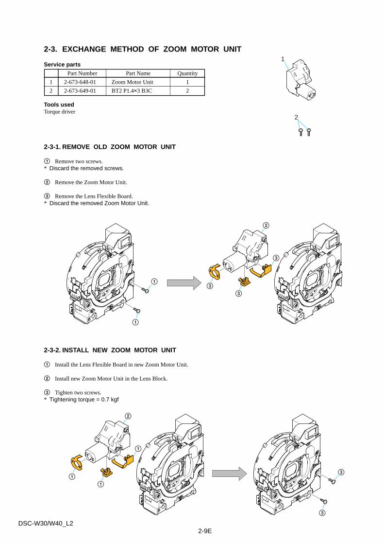
2-3-1. REMOVE OLD ZOOM MOTOR UNIT
1 Remove two screws.* Discard the removed screws.
2 Remove the Zoom Motor Unit.
3 Remove the Lens Flexible Board.* Discard the removed Zoom Motor Unit.
2-3-2. INSTALL NEW ZOOM MOTOR UNIT
1 Install the Lens Flexible Board in new Zoom Motor Unit.
2 Install new Zoom Motor Unit in the Lens Block.
3 Tighten two screws.* Tightening torque = 0.7 kgf
1
2
3
3
11
1
2
1
1
33
3
2
HELPDSC-W30/W40_L2
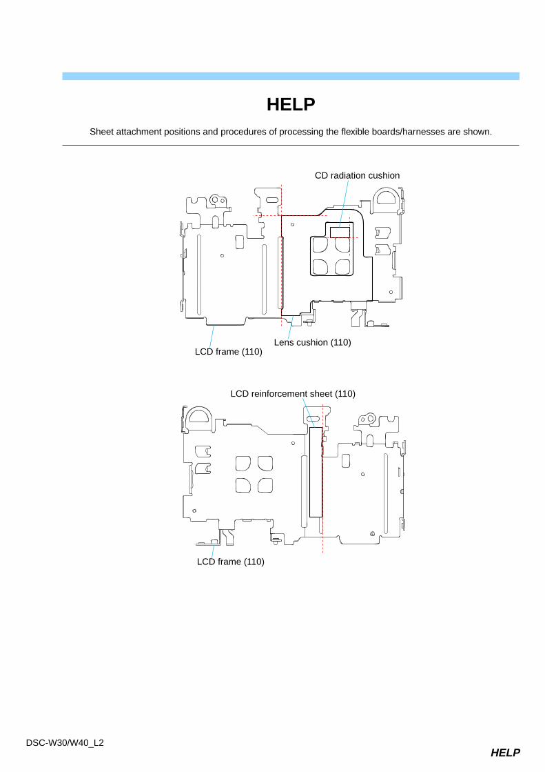
HELPSheet attachment positions and procedures of processing the flexible boards/harnesses are shown.
Lens cushion (110)LCD frame (110)
LCD reinforcement sheet (110)
LCD frame (110)
CD radiation cushion
DSC-W30/W40_L2
LinkLink
3. BLOCK DIAGRAMS
OVERALL BLOCK DIAGRAM (2/2)
OVERALL BLOCK DIAGRAM (1/2) POWER BLOCK DIAGRAM
DSC-W30/W40_L23-1
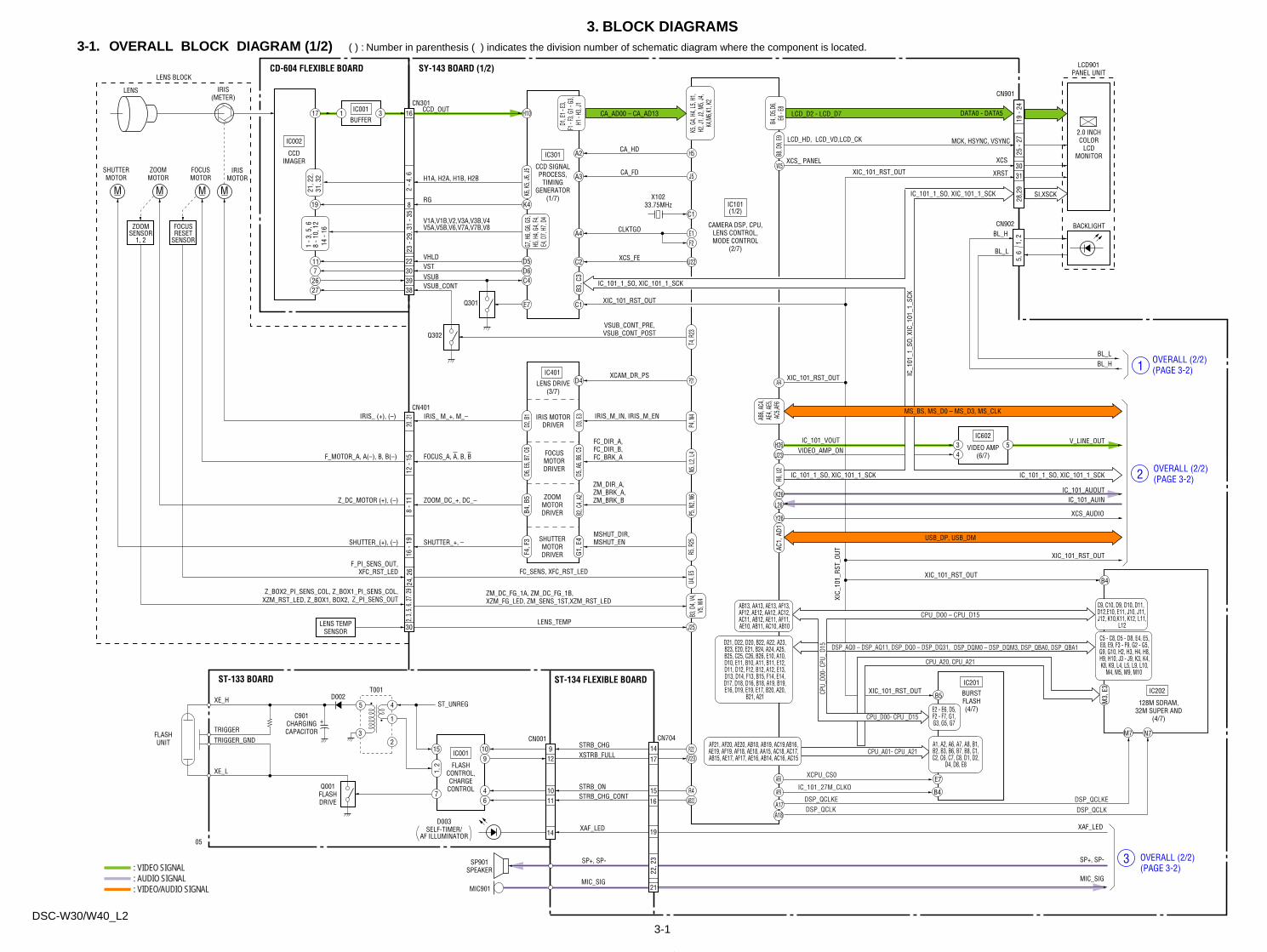
3. BLOCK DIAGRAMS3-1. OVERALL BLOCK DIAGRAM (1/2) ( ) : Number in parenthesis ( ) indicates the division number of schematic diagram where the component is located.
A : VIDEO SIGNALA : AUDIO SIGNALA : VIDEO/AUDIO SIGNAL
SY-143 BOARD (1/2)
XCS_FE
VSUB_CONT_PRE,VSUB_CONT_POST
F2
U22
E1CLKTGOCAMERA DSP, CPU,
LENS CONTROL,MODE CONTROL
(2/7)
J5CA_FD
H5CA_HD
CA_AD00 – CA_AD13
LENS
CCDIMAGER
IC002
IC001
CD-604 FLEXIBLE BOARD
17 31 H10
K4
LENS BLOCK
CN301
ZOOMMOTOR
M
FOCUSMOTOR
M
FOCUSRESET
SENSOR
ZOOMSENSOR
1, 2
23 -
29, 3
1 - 3
5
K6, K
5, J6
, J5
16
LENS TEMPSENSOR
BUFFER
11
19
72230
D5D6
8
1 - 3
, 5, 6
14 -
168
- 10,
12
21,
22,
31, 3
2
2 -
4, 6
CCD_OUT
V1A,V1B,V2,V3A,V3B,V4V5A,V5B,V6,V7A,V7B,V8
H1A, H2A, H1B, H2B
VHLDVST
3938
RG
27
Q302
CCD SIGNALPROCESS,
TIMINGGENERATOR
(1/7)
IC301
26 C4
E7
VSUBVSUB_CONT
Q301
A4
C2
XIC_101_RST_OUTC1
XCAM_DR_PSP21D4
A3
A2
B3, C
3
T4, R
23
J25LENS_TEMP
IRIS(METER)
IRISMOTOR
M
SHUTTERMOTOR
M
IC401
20, 2
112
- 15
8 - 1
116
- 19
24, 2
62,
3, 5,
6, 27
. 29
FOCUSMOTORDRIVER
IRIS_M_IN, IRIS_M_EN
FC_DIR_A, FC_DIR_B, FC_BRK_A
ZM_DIR_A,ZM_BRK_A,ZM_BRK_B
MSHUT_DIR,MSHUT_EN
FC_SENS, XFC_RST_LED
ZM_DC_FG_1A, ZM_DC_FG_1B,XZM_FG_LED, ZM_SENS_1ST,XZM_RST_LED
ZOOMMOTORDRIVER
SHUTTERMOTORDRIVER
IRIS MOTORDRIVER
F_MOTOR_A, A(–), B, B(–)
Z_DC_MOTOR (+), (–) ZOOM_DC_+, DC_–
SHUTTER_(+), (–)
F_PI_SENS_OUT,XFC_RST_LED
Z_BOX2_PI_SENS_COL, Z_BOX1_PI_SENS_COL,Z_PI_SENS_OUTXZM_RST_LED, Z_BOX1, BOX2,
SHUTTER_+, –
IRIS_ M_+, M_–IRIS_ (+), (–)CN401
FOCUS_A, A, B, B
D2,
B1D6
, E6,
B7, C
6B4
, B5
F4, F
3
G1, E
4
LENS DRIVE(3/7)
30
ST-133 BOARD ST-134 FLEXIBLE BOARD
R4
05
V23R22
STRB_CHG
XAF_LED
MIC_SIG
XSTRB_FULL
ST_UNREG
Q001FLASHDRIVE
SP901SPEAKER
MIC901
FLASHUNIT
FLASHCONTROL,CHARGE
CONTROL
6
910
7
IC001
XE_H
TRIGGERTRIGGER_GND
XE_L
+C901
CHARGINGCAPACITOR
D002
3
5 4
1
215
T001
STRB_CHG_CONT4 STRB_ON
CN704CN001
12 17
22, 2
3
21
9 14
11 16
14 19
10 15
D003SELF-TIMER/
AF ILLUMINATOR
SP+, SP-
XAF_LED
MIC_SIG
SP+, SP-
IC_101_AUOUT
XIC_101_RST_OUT
XIC_101_RST_OUT
XIC_101_RST_OUT
XIC_101_RST_OUT
XIC_
101_
RST_
OUT
XIC_101_RST_OUT
2 OVERALL (2/2)(PAGE 3-2)
USB_DP, USB_DM
AF4
W25
AE6
AF9AB22
BACKLIGHT
2.0 INCHCOLOR
LCDMONITOR
CN901
CN902
LCD901PANEL UNIT
IC101(1/2)
IC_101_AUINK26
L26
Y26
H26U23
XCS_AUDIO
BL_L
BL_L
BL_H
BL_H
OVERALL (2/2)(PAGE 3-2)1
OVERALL (2/2)(PAGE 3-2)
3
LCD_HD, LCD_VD,LCD_CK MCK, HSYNC, VSYNC
LCD_D2 - LCD_D7 DATA0 - DATA5
IC202IC201
128M SDRAM,32M SUPER AND
(4/7)
BURSTFLASH(4/7)
M7
B4
B4
E7
B5
DSP_QCLKE DSP_QCLKEDSP_QCLK DSP_QCLK
IC_101_27M_CLKO
XCPU_CS0
N7
A18A17
DSP_AQ0 – DSP_AQ11, DSP_DQ0 – DSP_DQ31, DSP_DQM0 – DSP_DQM3, DSP_QBA0, DSP_QBA1
CPU_D00 – CPU_D15
CPU_
D00-
CPU
_ D1
5
CPU_D00- CPU _D15
CPU_A01- CPU_A21
C5 - C8, D5 - D8, E4, E5,E8, E9, F3 - F9, G2 - G5,G9, G10, H2, H3, H4, H8,H9, H10, J3 - J9, K3, K4,K8, K9, L4, L5, L9, L10,
M4, M5, M9, M10
D21, D22, D20, B22, A22, A23,B23, E20, E21, B24, A24, A25,B25, C25, C26, B26, E10, A10,D10, E11, B10, A11, B11, E12,D11, D12, F12, B12, A12, E13,D13, D14, F13, B15, F14, E14,D17, D18, D16, B18, A19, B19,E16, D19, E19, E17, B20, A20,
B21, A21
AB13, AA13, AE13, AF13,AF12, AE12, AA12, AC12,AC11, AB12, AE11, AF11,AE10, AB11, AC10, AB10
E2 - E6, D5,F2 - F7, G1,G3, G5, G7
A1, A2, A6, A7, A8, B1,B2, B3, B6, B7, B8, C1,C2, C6, C7, C8, D1, D2,
D4, D8, E8
C9, C10, D9, D10, D11, D12,E10, E11, J10, J11, J12, K10,K11, K12, L11,
L12
AF21, AF20, AE20, AB18, AB19, AC19,AB16,AE19, AF19, AF18, AE18, AA15, AC18, AC17,AB15, AE17, AF17, AE16, AB14, AC16, AC15
XCS_ PANEL XCS
XRST
IC_101_1_SO, XIC_101_1_SCK
IC_101_1_SO, XIC_101_1_SCKIC_101_1_SO, XIC_101_1_SCK
IC_1
01_1
_SO,
XIC
_101
_1_S
CK
IC_101_1_SO, XIC_101_1_SCK SI,XSCK
V_LINE_OUTVIDEO_AMP_ON
IC_101_VOUTVIDEO AMP
(6/7)
534
IC602
MS_BS, MS_D0 – MS_D3, MS_CLK
G7, H
6, G6
, G5,
H5, H
4, G4
, F4,
E4, D
7, H7
, D4
D1, E
1 - E3
,F1
- F3
, G1 -
G3,
H1 -
H3, J
1
K5, G
4, H4
, L5,
H1,
H2, J
1, J2
, M5,
J4,
K4,M
6,K1,
K2
D3, E
3D5
, A6,
B6, C
5
R5, R
25U4
, E5
AC1,
AD1
R6, U
2B8
, D9,
E9
AB6,
AC4,
AE4,
AE5,
AC5,A
F6B4
, D5,D
6,E6
- E8
N5, L
2, L4
P5, N
2, N6
B2, C
4, A2
P4, N
4B3
, D4,
V4,
V5, W
4
1, 2
3130
28,2
91,
25,
625
- 27
19 -
24
CPU_A20, CPU_A21
M3,
E3
X10233.75MHz
C1
DSC-W30/W40_L23-2
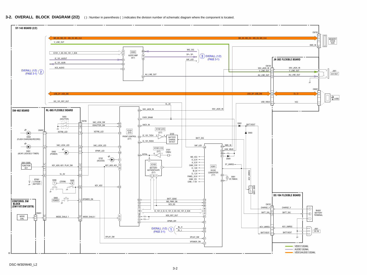
3-2. OVERALL BLOCK DIAGRAM (2/2) ( ) : Number in parenthesis ( ) indicates the division number of schematic diagram where the component is located.
A : VIDEO SIGNALA : AUDIO SIGNALA : VIDEO/AUDIO SIGNAL
SY-143 BOARD (2/2)
XAV_JACK_IN XAV_JACK_IN
XAV_JACK_IN
VCC
V_LINE_OUT V_LINE_OUT
AU_LINE_OUT AU_LINE_OUTAU_LINE_OUT
USB_VBUS
D+, D-USB_DP, USB_DM
1
JK-302 FLEXIBLE BOARD
DC-104 FLEXIBLE BOARD
AUDIO AMP(6/7)
IC603
E6
D1
B6
05
V_LINE_OUT
IC_101_AUOUT
SP+, SP-
MIC_SIG
IC_101_AUIN
XCS_AUDIO
XIC_101_RST_OUT
E5
E4
2OVERALL (1/2)(PAGE 3-1)
S003(SHUTTER)
T W(ZOOM)
BATTERYCHARGEDETECT
Q1023 4
6 1
XPOWER_ON
KEY_AD2
XPOWER_ON
XPLAY_SWXPLAY_SW
6 - 8
XAE_LOCK_SW
XAE_LOCK_LEDXAE_LOCK_LED
MODE_DIAL0,1MODE_DIAL0, 1
KEY_AD0, AD1
D002(POWER)
D001(AE/AF LOCK/SELF-TIMER)
USB_DP, USB_DM
DC/DCCONVERTER
(7/7)
IC001
IC102 (2/2)
D_3.2V
PANEL_8.5V
ST_UNREG
MS_VCC
A_3.2V
D_1.8VCAM_2.9V
CAM_–7.5VCAM_12V
D_1.2VM_5V
IC101_1_SO, XIC_101_1_SCK
F3, E
3
A5, A
2
XAV_JACK_IN
USB_VBUS
XMS_IN
IC_101_0_SI, IC_101_0_SO, XIC_101_0_SCK
A9
A8
X00132.768kHz
D003
D004
D001
CN002
CN705
CN001
2
3
1
XSTRB_LEDXSTRB_LED
XSHUTTER_SW
POWERS002
S001-S009
S005S006
+
–
BH001BATTERY
TERMINAL
VL_3V
VL_3V
EVER_SRAM
S
X10112MHzD23
E4
AA23
W23
H25
U25
AB25
AA26
V25
F22
E22
F9
OVERALL (1/2)(PAGE 3-1)
3
OVERALL (1/2)(PAGE 3-1)
1 BL_L
C7
D7
XPWR_OFF
XCS_DD A6T25K25
MS_PWR_ON D3
B10
C9
E9
A4
V1
A6
BL_H
N21P23
FUNCTIONKEY
MODEDIAL
D702(ACCESS)
D002(FLASH CHARGING/RECORD)
B7
BATT_SENS D4
R26
Y4
XDD_RST_OUT A7
B8H1
XAF_LED
XAF_LED
SW-462 BOARD RL-065 FLEXIBLE BOARD
CONTOROL SW BLOCK(SW110T/SW120TB)
IC101(2/2)
FRONT CONTROL(2/7)
(2/7)
IC102 (1/2)
(2/7)
IC103
BATTERYAUTHENTICATE
(2/7)
C6, C
5, B6
AA5,
AB5,
Y5
K23,
L23
L22,
L25
MS_BS, MS_D0 – MS_D3, MS_CLKMS_BS, MS_D0 – MS_D3, MS_CLK
CN703
CN702
CN001
CN701
MEMORYSTICKDUO
2 - 5,
7, 8
6
A/V OUTJ001
DC INJ001
XMS_IN
BATT/XEXTXACV_IN
IC_101_RXD4
EXTAL
IC_101_TXD4BATT_SIG
ACV_
UNRE
G
ACV_UNREG ACV_UNREG
BATT/XEXT BATT/XEXT
CHARGE_V CHARGE_V
BATT_SIG BATT_SIG
1
10
BT001LITHIUMBATTERY
11 -
142
- 5
2, 3
8, 9
6
3
21
Q001
, Q00
2
4, 5
, 6
2, 3
, 411
, 12
1, 5
14, 1
5
1718
97
6
9
1
16
3
8
12
(USB)
KEY_AD0, AD1, PLAY_SW
XPWR_LED
DSC-W30/W40_L23-3E
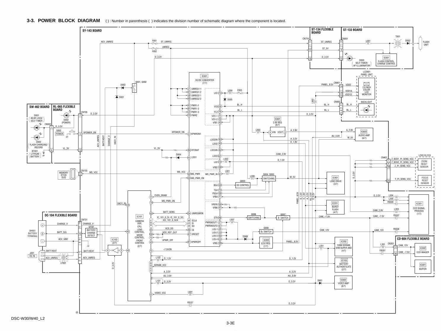
3-3. POWER BLOCK DIAGRAM ( ) : Number in parenthesis ( ) indicates the division number of schematic diagram where the component is located.
05
SY-143 BOARD
SW-462 BOARD RL-065 FLEXIBLE BOARD
DC-104 FLEXIBLE BOARD
ST-134 FLEXIBLE BOARD
ST-133 BOARD
VO1-1D_3.2V
A_3.2V
A_2.9V A_2.9V
PANEL_8.5V
PANE
L_8.
5V
LX2
PWR1-1A1
UNREG1-2K1UNREG1-1J1
F1VO1-2 F2VFB1 H2
BG4 G9
PSG4 G8VFB4 F7
TG4 F10
C10
VFB2 D8
IC001
DC/DC CONVERTER(7/7)
LDO2 A3
LX5-1 J9
LDO2IN B3
PWR2D10
UNREG2-1J6UNREG2-2K6
D_1.8V
D_1.
8V
D_1.2V
CAM_12V
CAM_–7.5V
PWR1-3C2PWR1-2B1
LDO3 A2
LDO3IN B2
PWR56OUT2 K7PWR56OUT1 J7
GT6 H6
VFB6 H7VREF6 G6
CAM_2.9V
MS_PWRG2 MS_PWR_IN G1MS_VCC
XPWRON1XPOWER_ONXPOWER_ON
LX5-4 K10LX5-3 K9LX5-2 J10
UNREG
L002
L001
M_5V
F002
F001
Q001, Q002
F003
CN704 CN001
BH001BATTERY
TERMINAL
CHARGE_V CHARGE_V
CHAR
GE_V
BATT_SIG
BATT/XEXT BATT/XEXT
ACV_GND
BATT
/XEX
T
ACV_UNREG
ACV_
UNRE
G
ACV_UNREG ACV_UNREG
BL_HVO3 E9
LX3 E10
BL_LVL3 F9
VFB5 H9
D005
D008
D002
L004
EVER_SRAM
XACV_IN
XACV
_IN
D004
D003
D001
BT001LITHIUMBATTERY
D003SELF-TIMER/
AF ILLUMINATOR
VL_3V VL_3V
Q004, Q005
SWITCHING
Q006SWITCHING
Q007B- SWITCH
Q008
B+ SWITCH
Q003
Q102BATTERYCHARGEDETECT
DC CONTROL
L006
B8 RTCBAT
H1
C7
LDO1
IC_101_0_SI, IC_101_0_SO,XIC_101_0_SCK
Y4
AA23XPWR_OFF
VIDEO_VCC
SDRAM_VCC
P25
G26
–7.5VON
W23 XCS_DDA6
T25
V1
V25
AA26
AB25
MS_PWR_ON
MS_PWR_OND3
B7
K25BATT_SENS UNREGMON
CE
D4
R26XDD_RST_OUT
A7
IC101
IC102
CAMERADSP,CPU,LENS
CONTROL,MODE
CONTROL,FRONT
CONTROL(2/7)
(2/7)
AA5, AB
5, Y5
A13, B1
3, D25,
D26
C6, C
5, B6
XPWROFF
XRESET
SCLKSISO
L007
ST_UNREG ST_UNREG
L102
L601
L101
AUDIO AMP(6/7)
VIDEO AMP(6/7)
IC603
D002(POWER)
IC602D_3.2V
D_3.2V
D_3.
2V
A_3.2V
A_3.
2V
AU_3.0V
AU_3
.0V
AU_3.0V
D_1.2V
D_1.
2V
D_3.2V
D_3.
2V
A_3.2V
AU_3.0V
D_1.2V
MS_VCC9
T001
FLASHUNIT
L001
2.0 INCHCOLOR
LCDMONITOR
LCD901PANEL UNIT
MEMORYSTICKDUO
CN703
CN705
CN002
CN701
FLASH CONTROL,CHARGE CONTROL
IC001
CAM_12V
CAM_–7.5V
CAM_2.9V
D_3.2V
D_3.
2V
CAM_12V
CAM_–7.5V
CN301
L303
L304L305
L301L201
FB307
FB107
CCD IMAGER
IC002
BUFFER
IC001
CCD SIGNALPROCESS
(1/7)
IC301
FB308
FB301
FB309
CD-604 FLEXIBLE BOARD
CN401Z_BOX1_PI_SENS_VCCZ_BOX2_PI_SENS_VCC
Z_PI_SENS_VCC
F_PI_SENS_VCC
IC201BURSTFLASH(4/7)
IC0028.5V REG
(7/7)
IC401LENS DRIVE
(3/7)
128M SDRAM,32M SUPER AND
(4/7)
IC202
BATTERYAUTHENTICATE
(2/7)
IC103
2.9V REG(6/7)
IC601
34 VOUTVIN
BACKLIGHTBL_H
CN902
CN901
BL_L
BL_H
BL_L
ST_5V
D_3.2VD_3.2V
D_3.2V
D_3.2V
PANEL_8.5V
VDD1D
VDD1A
VDD2
D601
34
L003
L902
LENS BLOCK
FOCUSRESET
SENSOR
ZOOMRESET
SENSOR
+
S
–
2 - 5
11 -
146
- 9
1
10
2
1
3
129
813
1 - 3
1 - 5
1318
1428
5, 6
1615
1, 2
14
25
12
36DC INJ001
LF001
POWERS002
M_5V
D001AE/AF LOCK/SELF-TIMER
D002FLASH CHARGING/
RECORD
DSC-W30/W40_L24-1
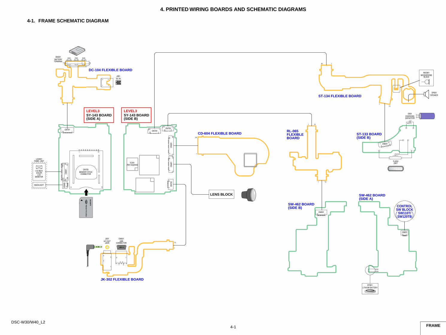
4-1. FRAME SCHEMATIC DIAGRAM
4. PRINTED WIRING BOARDS AND SCHEMATIC DIAGRAMS
FRAME
RL-065FLEXIBLEBOARD
MIC901MICROPHONE
BLOCK
BT001LITHIUM BATTERY
C901CHARGINGCAPACITOR
SP901SPEAKER
LENS BLOCK
J001DC IN
BH001BATTERY
TERMINAL
BACKLIGHT
LCD901PANEL UNIT
2.0 INCHCOLOR
LCDMONITOR
+
CN001USB
CONNECTOR
J001A/V OUT
JACK
IC201(Not supplied)
FLASHUNIT
CN703MEMORY STICK
CONNECTOR
39
1
1
1
19
12
DC-104 FLEXIBLE BOARD
LEVEL3SY-143 BOARD(SIDE B)
LEVEL3SY-143 BOARD(SIDE A)
114
123
114
CD-604 FLEXIBLE BOARD
ST-134 FLEXIBLE BOARD
ST-133 BOARD (SIDE B)
SW-462 BOARD(SIDE A)
SW-462 BOARD(SIDE B)
12
1314CN001
JK-302 FLEXIBLE BOARD
114
1 10
1211
232
133
CN701
CN90
11
6CN90
2
2 1
30 31
238
139
110
222
1231
218
19
CN40
1CN
301
CN70
2
CN704CN705
16CN001
CN002112
CONTROLSW BLOCK
SW110T/SW120TB
453
1
31
1
2 4
5
6 7
1
34
2
1
10
DSC-W30/W40_L2
CONTROL SW BLOCK (SW110T/SW120TB)
JK-302 FLEXIBLE BOARD (USB, A/V JACK)ST-134 FLEXIBLE BOARD
RL-065 FLEXIBLE BOARD (CONTROL SWITCH)
DC-104 FLEXIBLE BOARD (BATTERY IN, DC IN)
CD-604 FLEXIBLE BOARD (CCD IMAGER)
ST-133 BOARD (FLASH DRIVE)
SW-462 BOARD (CONTROL SWITCH)
LinkLink
4-2. SCHEMATIC DIAGRAMS
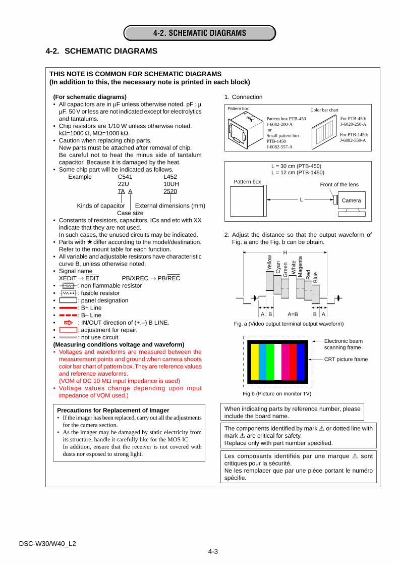
COMMON NOTE FOR SCHEMATIC DIAGRAMS
4-3DSC-W30/W40_L2
4-2. SCHEMATIC DIAGRAMS4-2. SCHEMATIC DIAGRAMS
4-2. SCHEMATIC DIAGRAMS
1. Connection
2. Adjust the distance so that the output waveform ofFig. a and the Fig. b can be obtain.
When indicating parts by reference number, pleaseinclude the board name.
(For schematic diagrams)• All capacitors are in µF unless otherwise noted. pF : µ
µF. 50 V or less are not indicated except for electrolyticsand tantalums.
• Chip resistors are 1/10 W unless otherwise noted.kΩ=1000 Ω, MΩ=1000 kΩ.
• Caution when replacing chip parts.New parts must be attached after removal of chip.Be careful not to heat the minus side of tantalumcapacitor, Because it is damaged by the heat.
• Some chip part will be indicated as follows.Example C541 L452
22U 10UHTA A 2520
• Constants of resistors, capacitors, ICs and etc with XXindicate that they are not used.In such cases, the unused circuits may be indicated.
• Parts with differ according to the model/destination.Refer to the mount table for each function.
• All variable and adjustable resistors have characteristiccurve B, unless otherwise noted.
• Signal nameXEDIT → EDIT PB/XREC → PB/REC
• 2: non flammable resistor• 5: fusible resistor• C: panel designation• A: B+ Line• B: B– Line• J : IN/OUT direction of (+,–) B LINE.• C: adjustment for repair.• A: not use circuit(Measuring conditions voltage and waveform)• Voltages and waveforms are measured between the
measurement points and ground when camera shootscolor bar chart of pattern box. They are reference valuesand reference waveforms.(VOM of DC 10 MΩ input impedance is used)
• Voltage values change depending upon inputimpedance of VOM used.)
Kinds of capacitorCase size
External dimensions (mm)
Yello
w
A AB BA=B
Fig. a (Video output terminal output waveform)
H
Cya
nG
reen
Whi
teM
agen
ta
Red
Blu
e
Fig.b (Picture on monitor TV)
CRT picture frame
Electronic beamscanning frame
THIS NOTE IS COMMON FOR SCHEMATIC DIAGRAMS(In addition to this, the necessary note is printed in each block)
Pattern box
Pattern box PTB-450J-6082-200-A orSmall pattern boxPTB-1450J-6082-557-A
Color bar chart
For PTB-450:J-6020-250-A
For PTB-1450:J-6082-559-A
Pattern box Front of the lens
L = 30 cm (PTB-450)L = 12 cm (PTB-1450)
L Camera
Precautions for Replacement of Imager• If the imager has been replaced, carry out all the adjustments
for the camera section.• As the imager may be damaged by static electricity from
its structure, handle it carefully like for the MOS IC.In addition, ensure that the receiver is not covered withdusts nor exposed to strong light.
The components identified by mark 0 or dotted line withmark 0 are critical for safety.Replace only with part number specified.
Les composants identifiés par une marque 0 sontcritiques pour la sécurité.Ne les remplacer que par une pièce portant le numérospécifie.
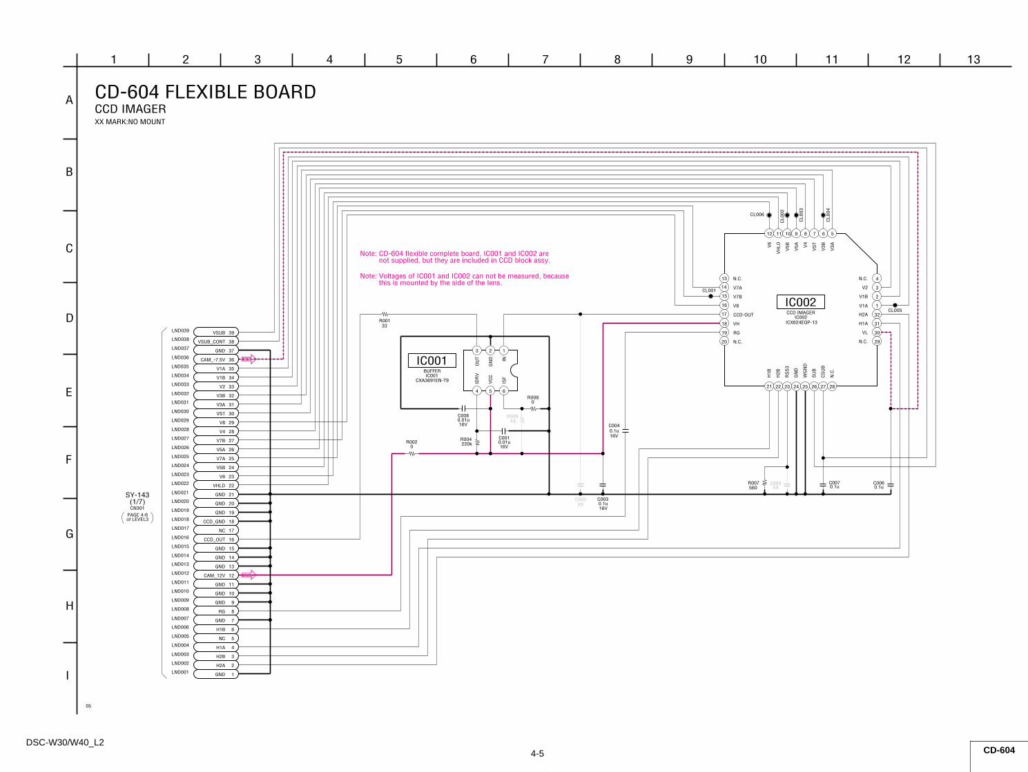
DSC-W30/W40_L24-5 CD-604
XXR009
XXC002
C005XX
Note: CD-604 flexible complete board, IC001 and IC002 are not supplied, but they are included in CCD block assy.
Note: Voltages of IC001 and IC002 can not be measured, because this is mounted by the side of the lens.
LND004 H1A
LND010 GND
R0020
LND012 CAM_12V
IC002ICX624EQP-13
1V1A
2V1B
3V2
4N.C.
7
VS
T
8
V4
9
V5A
10
V5B
11
VH
LD
12
V6
13 N.C.
14 V7A
15 V7B
16 V8
17 CCD-OUT
18 VH
19 RG
20 N.C.
21
H1B
22
H2B
23
RS
S3
24
GN
D
25
WG
ND
26
SU
B
27
CS
UB
28
N.C
.
29N.C.
30VL
31H1A
32H2A
5
V3A
6
V3B
C0070.1u
LND024 V5B
LND027 V7BLND026 V5A
CL0
04
LND033 V2
LND016 CCD_OUT
LND028 V4
0.01uC001
16V
LND037 GND
LND034 V1B
LND015 GND
C0060.1u
LND014 GND
R007560
LND017 NC
LND029 V8
LND013 GND
LND025 V7A
R00133
LND009 GND
16V0.1uC004
LND023 V6
LND011 GND
LND006 H1B
LND022 VHLD
LND039 VSUB
CL0
02CL006
LND007 GND
LND001 GND
CL0
03
LND008 RG
LND019 GND
LND002 H2A
LND030 VST
LND038 VSUB_CONT
LND018 CCD_GND
LND036 CAM_-7.5V
LND020 GND
CL005
IC001CXA3691EN-T9
1
IN
2
GN
D
3
OU
T
4
IDR
V
5
VC
C
6
ISF
220kR004
LND005 NC
LND021 GND
LND032 V3B
LND035 V1A
LND031 V3A
16V
C0030.1u
LND003 H2B
CL001
R0080
0.01u16V
C008
33
29
10
14
19
36
7
38
34
16
1
12
18
2
35
9
26
25
39
13
17
32
4
3
30
5
28
15
8
23
24
22
27
31
20
21
11
37
6
CCD IMAGER
IC001BUFFER
IC002
1 5
G
A
6 12104
05
98 117
CD-604 FLEXIBLE BOARD
B
I
E
13
XX MARK:NO MOUNT
3
D
F
H
C
CCD IMAGER
2
(1/7)
PAGE 4-6of LEVEL3
SY-143
CN301
DSC-W30/W40_L2
Schematic diagrams of the SY-143 board are not shown.Pages from 4-6 to 4-12 are not shown.
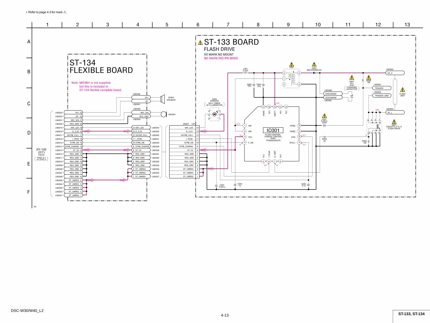
DSC-W30/W40_L24-13 ST-133, ST-134
• Refer to page 4-3 for mark 0.
NO MARK:REC/PB MODE
Note: MIC901 is not supplied,but this is included inST-134 flexible complete board.
3.2
0
0.1 0
0
4.2
5 0.1
4.2
250
0.1uC005
1 SW
2 SW
3 VCC
4 F_ON
5
N.C
6
I_P
EAK
7
G_I
GB
T
8
N.C
9XFULL
10CHG
11PGND
12PGND
13
N.C
14
N.C
15
VB
ATT
16
N.C
17
HG
ND
LND006
DISCHARGE
L0012.2uH
LND004
XE_L
33R003
1MR005
22uC002 LND001
TRIGGER
1MR004
LND005
DISCHARGE
TIG022TS-S-TL-EQ001
1
8 5
234
67
1uC004
22uC003
T001
4
1
2 3
5
LND002
TRIGGER_GND
0.001uC001
14PCN001
1ST_UNREG
2ST_UNREG
3ST_UNREG
4REG_GND
5REG_GND
6REG_GND
7REG_GND
8ST_5V
9STRB_CHARGE
10STRB_ON
11I_PEAK
12XSTRB_FULL
13D_3.2V
14XAF_LED
LND003
XE_H
MA2YF8000LS0D002
1
2
34
5
6
250V0.047uC007
LND031
LND013
LND014
LND021
LND001
LND036
LND044
LND015
LND002
LND003
LND043
LND005
LND009
LND012
LND033LND008
LND018
LND039
LND037
LND022
LND019
LND035
LND004
LND047
LND038
LND006
LND045
LND042
LND034
LND010
LND007
LND048
LND023
LND016
LND040
LND032
LND046
LND020
LND011
LND041
LND017
MIC_SIG
XAF_LED
REG_GND
STRB_CHARGE
REG_GND
REG_GND
D_3.2V
ST_UNREG
SP-
STRB_ON
ST_UNREG
REG_GND
XAF_LED
REG_GND
XSTRB_FULL
ST_UNREG
XSTRB_FULL
D_3.2V
REG_GND
I_PEAK
REG_GND
ST_UNREG
SP+
REG_GND
STRB_ON
REG_GND
REG_GND
ST_5V
ST_UNREG
I_PEAK
ST_UNREG
REG_GND
SP-
ST_5V
REG_GND
MIC_SIG
ST_UNREG
REG_GND
ST_UNREG
SP+
FLEXIBLE BOARD
SP901SPEAKER
MIC901
13
19
12
11
6
18
2
4
9
5
16
22
14
10
20
21
8
17
15
3
23
7
1
10
9
11
3
5
6
13
1
7
8
2
12
14
4
ST-134
FLASH DRIVE
UNITFLASH
9 11
A
05
E
5 132 6
B
1210
F
4
C
71 3
D
8
FLASH DRIVEST-133 BOARDXX MARK:NO MOUNT
DOR5352D003
SELF-TIMER/AF ILLUMINATOR
C90197u
315VCHARGINGCAPACITOR
SY-143(2/7)CN704
PAGE 4-7of LEVEL3
STRB_CHARGE
TPS65552RGTRIC001
IC001FLASH CONTROL,
CHARGE CONTROL
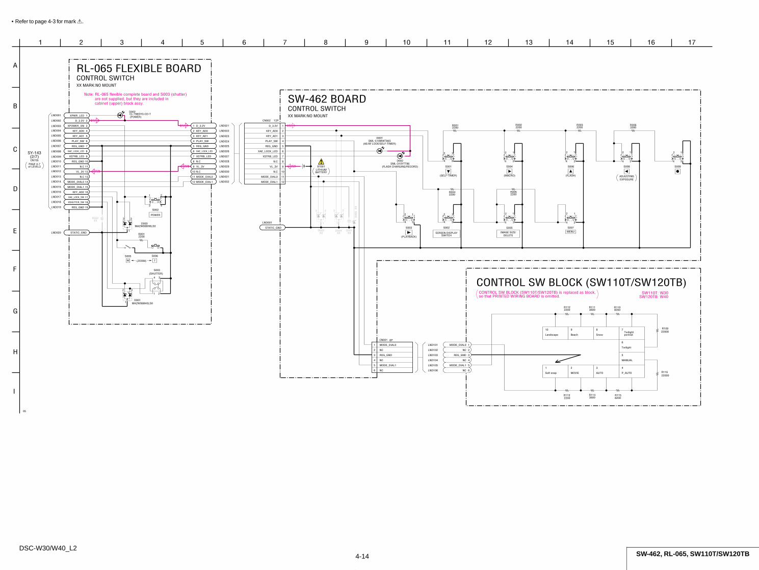
DSC-W30/W40_L24-14 SW-462, RL-065, SW110T/SW120TB
R002XX
D00
5X
X
XXD003
3 2
1
XXD004
3 2
1
XXC001
Note: RL-065 flexible complete board and S003 (shutter) are not supplied, but they are included in cabinet (upper) block assy.
CONTROL SW BLOCK (SW110T/SW120TB) is replaced as block,so that PRINTED WIRING BOARD is omitted.
W30W40SW120TB:
SW110T:
8
E
5 7
G
41
H
C
6
A
11
B
9 103
D
F
122
I
05
13 14 15 16 17
XX MARK:NO MOUNT
CONTROL SWITCHRL-065 FLEXIBLE BOARD
LND020
CL-196SYG-CD-TD002
LND014 MODE_DIAL0
LND009 XSTRB_LED
LND003 XPOWER_ON
LND017 XAE_LOCK_SW
LND005 KEY_AD1
LND018 XSHUTTER_SW
LND012 VL_3V
LND013 N.C
MAZW068H0LS0D003
32
1
MAZW068H0LS0D001
32
1
LND002 D_3.2V
LND006 PLAY_SW
LND011 N.C
LND008 XAE_LOCK_LED
LND015 MODE_DIAL1
STATIC_GND
2200R001
LND019 REG_GND
1
3
2
4
LND007 REG_GND
LND001 XPWR_LED
LND010 REG_GND
LND016 KEY_AD2
LND004 KEY_AD0
S003
4
1 2
3
LND021D_3.2V
LND029VL_3V
LND028N.C
LND023KEY_AD1
LND031MODE_DIAL0
LND026XAE_LOCK_LED
LND022KEY_AD0
LND030N.C
LND027XSTRB_LED
LND032MODE_DIAL1
LND024PLAY_SW
LND025REG_GND
(POWER)
(ZOOM)
(SHUTTER)
14
3
5
11
2
8
16
15
7
1
17
10
9
18
6
4
12
13
19
3
5
11
2
8
7
1
10
9
6
4
12
PAGE 4-7CN705
of LEVEL3
(2/7)SY-143
S002
POWER
S005
W
S006
T
6PCN001
1 MODE_DIAL0
2 NC
3 REG_GND
4 NC
5 MODE_DIAL1
6 NC
2200R001
2200R002
2200R004
2200R005
2200R003
3300R006
LND001
STATIC_GND
12PCN002
1D_3.2V
2KEY_AD0
3KEY_AD1
4PLAY_SW
5REG_GND
6XAE_LOCK_LED
7XSTRB_LED
8N.C
9VL_3V
10N.C
11MODE_DIAL0
12MODE_DIAL1
1
3
2
4
1
3
2
4
1
3
2
4
S004
1
3
2
4
S005
1
3
2
4
S006
1
3
2
4
S007
1
3
2
4
1
3
2
4
S009
1
3
2
4
R1122200
R1113600
R1108200
R1132200
R1143600
R1158200
R11622000
R10922000
(FLASH)(MACRO)
IMAGE SIZE/DELETE
MENU
LND101
LND102
LND103
LND104
LND105
LND106
10
Landscape
9
Beach
8
Snow
7Twilightportrait
6
Twilight
5
MANUAL
4
P_AUTO
3
AUTO
2
MOVIE
1
Soft snap
CONTROL SW BLOCK (SW110T/SW120TB)
SW-462 BOARDCONTROL SWITCHXX MARK:NO MOUNT
BT001LITHIUMBATTERY
SML-510MWT86SD001
(AE/AF LOCK/SELF-TIMER)
SML-310YTT86D002
(FLASH CHARGING/RECORD)
S003
(PLAYBACK)
S002
SCREEN DISPLAYSWITCH
S001
(SELF-TIMER)
S008
ADJUSTINGEXPOSURE
MODE_DIAL0
NC
REG_GND
NC
MODE_DIAL1
NC
1
2
3
4
5
6
• Refer to page 4-3 for mark 0.
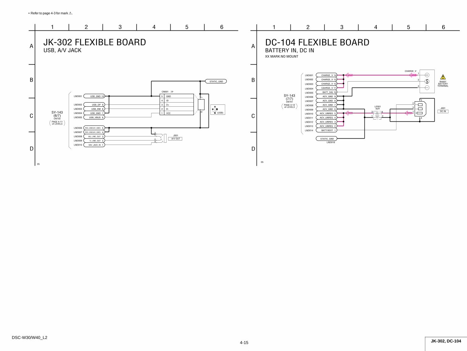
DSC-W30/W40_L24-15 JK-302, DC-104
• Refer to page 4-3 for mark 0.
LND012 ACV_UNREG
LND005 BATT_SIG
LND011 ACV_UNREG
LND004 CAHRGE_V
LND010 ACV_UNREG
LND003 CHARGE_V
LND009 ACV_GND
LND002 CHARGE_V
LND018
STATIC_GND
LND001 CHARGE_V
J001
1
3
2
4
5
LND008 ACV_GND
LND014 BATT/XEXT
LND007 ACV_GND
LND013 ACV_UNREG
LND006 ACV_GND
LF0010uH
21
3 4
2
1
3
BH001BATTERY
TERMINAL
DC IN
CHARGE_V
05
XX MARK:NO MOUNT
1
D
B
DC-104 FLEXIBLE BOARDA
53
C
62
BATTERY IN, DC IN
4
(7/7)
of LEVEL3PAGE 4-12
SY-143
CN701
S
1
12
10
4
13
7
8
14
5
6
9
11
3
2
LND004
LND003
LND007
LND008
LND005
LND001
LND009
LND002
LND010
LND006
1
2
3
4
7PCN001
1 VCC
2 D-
3 D+
4 ID
5 GND
67
REG_GND(AV_GND)
USB_GND
XAV_JACK_IN
USB_DM
USB_GND
USB_DP
USB_VBUS
AU_LINE_OUT
V_LINE_OUT
REG_GND(AV_GND)
STATIC_GND
J001A/V OUT
(USB)
USB, A/V JACK
4
JK-302 FLEXIBLE BOARD
05
1
D
B
A
53
C
62
1
4
10
3
7
6
9
5
2
8
SY-143
PAGE 4-11CN702(6/7)
of LEVEL3
DSC-W30/W40_L2
LinkLink
4-3. PRINTED WIRING BOARDS
CD-604 FLEXIBLE BOARD
ST-134 FLEXIBLE BOARD
ST-133 BOARD
SW-462 BOARD
JK-302 FLEXIBLE BOARD
RL-065 FLEXIBLE BOARD
DC-104 FLEXIBLE BOARD
MOUNTED PARTS LOCATIONCOMMON NOTE FOR PRINTED WIRING BOARDS
4-17DSC-W30/W40_L2
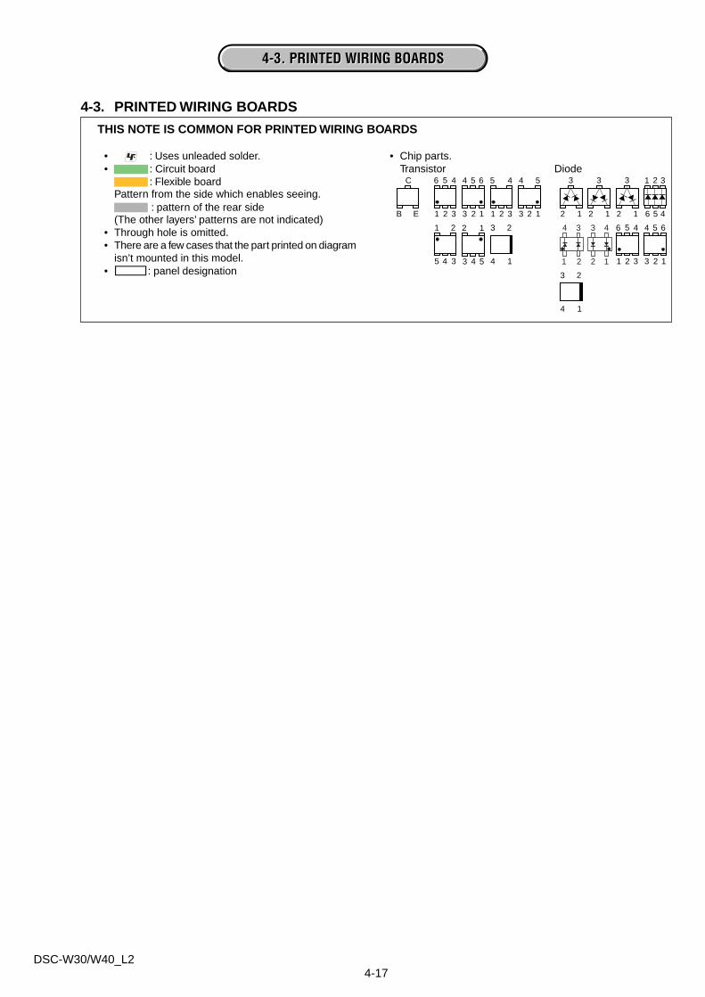
4-3. PRINTED WIRING BOARDS4-3. PRINTED WIRING BOARDS
4-3. PRINTED WIRING BOARDS
• : Uses unleaded solder.• : Circuit board
: Flexible boardPattern from the side which enables seeing.
: pattern of the rear side(The other layers’ patterns are not indicated)
• Through hole is omitted.• There are a few cases that the part printed on diagram
isn’t mounted in this model.• C: panel designation
THIS NOTE IS COMMON FOR PRINTED WIRING BOARDS
2 1
3
2 1
3
2 1
3
345
21
123
654
EB
C
31
5
2
46
123
654
31
5
2
46
123
54
4 3
1 2
31 2
45
53 4
12
14
23
46
2
5
31
12
43
14
23
• Chip parts.Transistor Diode
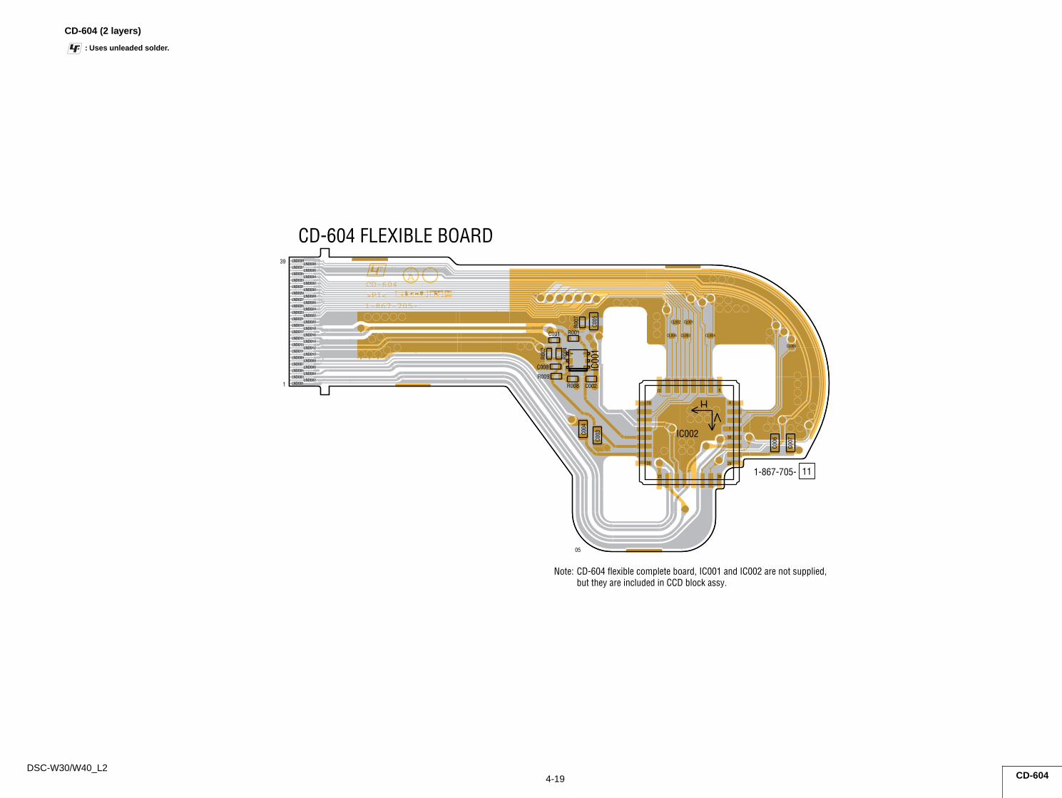
DSC-W30/W40_L24-19 CD-604
CD-604 (2 layers)
: Uses unleaded solder.
1-867-705-1 867 7051 867 7051 867 7051 867 7051 867 7051 867 7051 867 7051 867 705
AAA
>PI<PIPI>PI<>PI<>PI<>PI<>PI<PICD-604CD 604CD 604CD 604CD 604CD 604CD 604CD 604CD 604
29
32
4
1
20
13
512
21 28
13
64
C001
C002
C003C0
04
C005
C006
C007
C008
IC002
CL001CL002
CL003 CL004
CL005
CL006R001
R002
R004
R007
R008
R009
IC00
1
LND001LND002
LND003LND004
LND005LND006
LND007LND008
LND009LND010
LND011LND012
LND013LND014
LND015LND016
LND017LND018
LND019LND020
LND021LND022
LND023LND024
LND025LND026
LND027LND028
LND029LND030
LND031LND032
LND033LND034
LND035LND036
LND037LND038
LND039
05
1
39
CD-604 FLEXIBLE BOARD
1-867-705- 11
Note: CD-604 flexible complete board, IC001 and IC002 are not supplied, but they are included in CCD block assy.
DSC-W30/W40_L2
Printed wiring boards of the SY-143 board are not shown.Page 4-20 is not shown.
DSC-W30/W40_L24-21 ST-133, ST-134
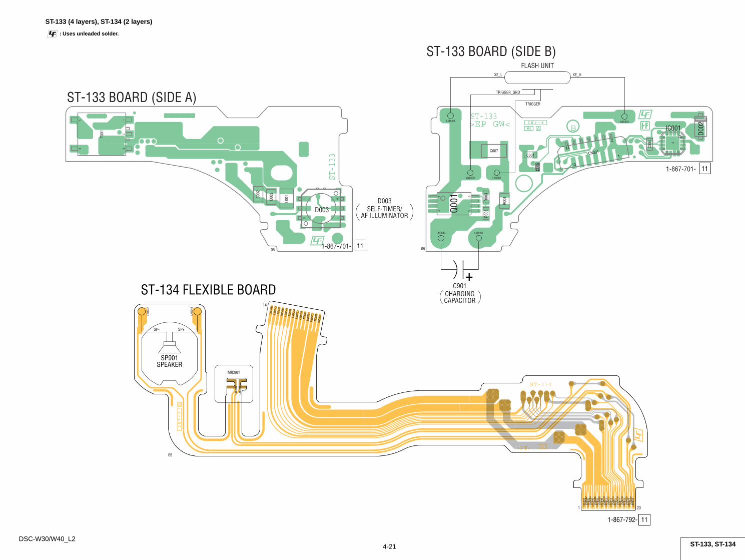
ST-133 (4 layers), ST-134 (2 layers)
: Uses unleaded solder.
ST-133
C002
C003
D003
T001
L001 1
3 46
45 1
23
05
ST-133 BOARD (SIDE A)
111-867-701-
D003SELF-TIMER/
AF ILLUMINATOR
ST-133B>EP GW<
1
2
13
14CN001
C001
C004
C005
C007
D002IC001
Q001 R0
03
R004
R005
5 16
13
14
129
17
8
85
14
LND001
LND006LND005
LND002
LND003LND004
05
ST-133 BOARD (SIDE B)
111-867-701-
FLASH UNITXE_L XE_H
TRIGGER_GND
TRIGGER
+C901
CHARGINGCAPACITOR
ST-134
>PI<>PI<>>>PI<
LND0
01LN
D002
LND0
03LN
D004
LND0
05LN
D006
LND0
07LN
D008
LND0
09LN
D010
LND0
11LN
D012
LND0
13LN
D014
LND0
15LN
D016
LND0
17LN
D018
LND0
19LN
D020
LND0
21LN
D022
LND0
23
LND0
31
LND0
32
LND0
33
LND0
34
LND0
35
LND0
36
LND0
37
LND0
38
LND0
39
LND0
40
LND0
41
LND0
42
LND0
43
LND0
44
LND0
45LN
D046
LND0
47
LND0
48
MIC901
SP901SPEAKER
SP- SP+
05
23
1
14
1
1-867-792- 11
ST-134 FLEXIBLE BOARD
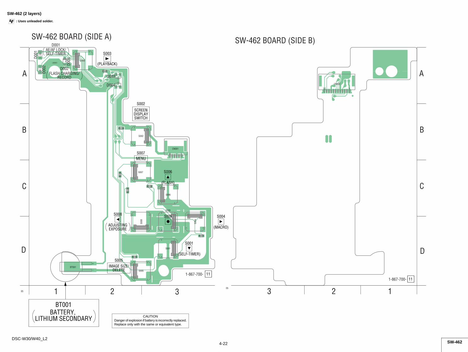
DSC-W30/W40_L24-22 SW-462
SW-462 (2 layers)
: Uses unleaded solder.
16
CN001
C001
BT001
S001
S002
S003
S004
S005
S006
S007
S008
D001
D002
D003
D004
D005
LND001
R001
R002
R003
R004
R005
R006
42
1 3
3
4 2
1
3 421
3
4 2
1
4 312
42
1 3
4
31
2
3
4 2
1
2
1 3
4AK
AK
S009
D
C
B
A
1 2 305
SW-462 BOARD (SIDE A)
111-867-700-
BT001BATTERY,
LITHIUM SECONDARY
(SELF-TIMER)
S001
(MACRO)
S004
(FLASH)
S006
S009
IMAGE SIZE/DELETE
S005
MENUS007
SCREENDISPLAYSWITCH
S002
1
1
3 2
2 3
+
-
S003
(PLAYBACK)
D001AE/AF LOCK/SELF-TIMER
D002FLASH CHARGING/
RECORD
ADJUSTINGEXPOSURE
S008
112
CN002
D
C
B
A
12305
SW-462 BOARD (SIDE B)
111-867-700-
CAUTIONDanger of explosion if battery is incorrectly replaced.Replace only with the same or equivalent type.
DSC-W30/W40_L24-23 RL-065, JK-302, DC-104
RL-065 (2 layers), JK-302 (2 layers), DC-104 (2 layers)
: Uses unleaded solder.
AAAA
-392-
RL-065 >PI<
S002
S005
S006
D001
D002
D003R001R002
S003
23
1
2 31
3 4
2 12 134
LND0
01LN
D002
LND0
03LN
D004
LND0
05LN
D006
LND0
07LN
D008
LND0
09LN
D010
LND0
11LN
D012
LND0
13LN
D014
LND0
15LN
D016
LND0
17LN
D018
LND0
19
LND020
LND0
21LN
D022
LND0
23LN
D024
LND0
25LN
D026
LND0
27LN
D028
LND0
29LN
D030
LND0
31LN
D032
05
RL-065 FLEXIBLE BOARD
1-868-392- 11S002POWER
S005W
S006T
S003(SHUTTER)
1
1 19
12
D002(POWER)
Note: RL-065 flexible complete board and S003 (shutter) are not supplied,but this is included in cabinet (upper) block assy.
>PI<
JK-302-
1
24
5
67
CN001
J001
1
3
4
2
LND001
LND002
LND003
LND004
LND005
LND006
LND007
LND008
LND009
LND010 LND012
05
10
1
JK-302 FLEXIBLE BOARD
1-867-706- 11
J001A/V OUT
CN001
(USB)
>PI<
DC-104
LF00
1
J001
LND0
01LN
D002
LND0
03LN
D004
LND0
05LN
D006
LND0
07LN
D008
LND0
09LN
D010
LND0
11LN
D012
LND0
13LN
D014
453
1
421
3
LND018
31
BH001
05
114
DC-104 FLEXIBLE BOARD
111-867-704-
S+ -
J001DC IN
DSC-W30/W40_L2
Mounted parts location of the SY-143 board are not shown.Page 4-25 is not shown.
4-26EDSC-W30/W40_L2
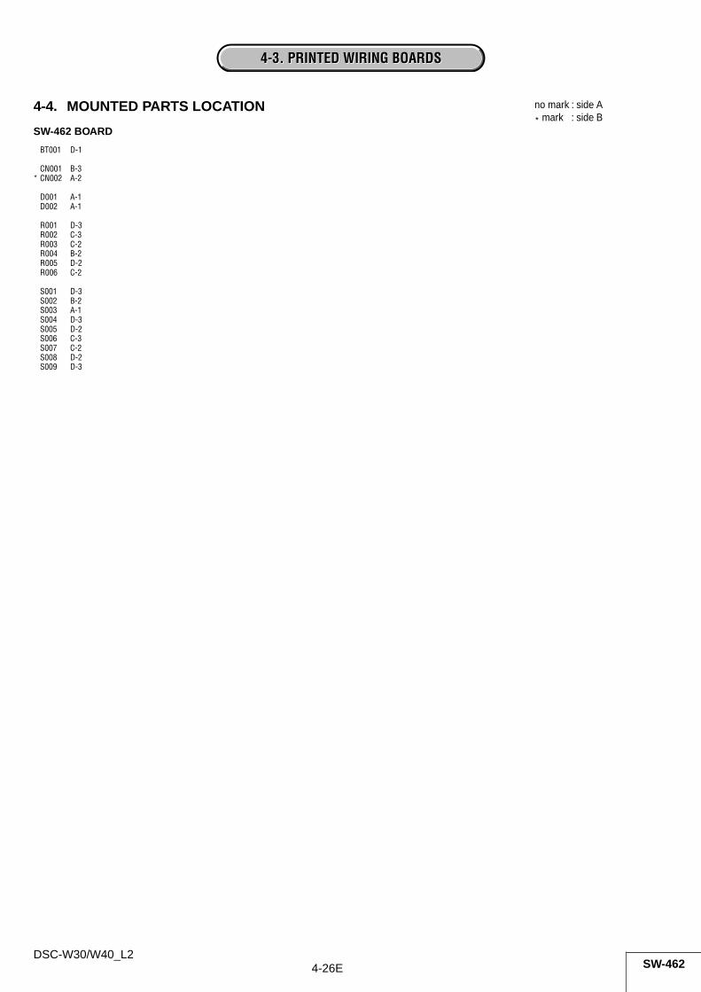
no mark : side A
* mark : side B
4-3. PRINTED WIRING BOARDS4-3. PRINTED WIRING BOARDS
SW-462
SW-462 BOARD
BT001 D-1
CN001 B-3* CN002 A-2
D001 A-1D002 A-1
R001 D-3R002 C-3R003 C-2R004 B-2R005 D-2R006 C-2
S001 D-3S002 B-2S003 A-1S004 D-3S005 D-2S006 C-3S007 C-2S008 D-2S009 D-3
4-4. MOUNTED PARTS LOCATION
NOTENOTE
DSC-W30/W40_L2
LinkLink
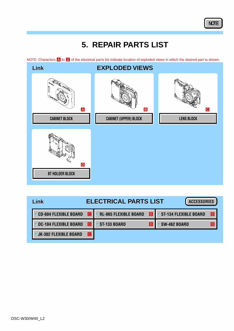
5. REPAIR PARTS LIST
LinkLink ELECTRICAL PARTS LISTELECTRICAL PARTS LIST
EXPLODED VIEWSEXPLODED VIEWS
ACCESSORIESACCESSORIES
NOTE: Characters A to Z of the electrical parts list indicate location of exploded views in which the desired part is shown.
A B C
CABINET BLOCK LENS BLOCKCABINET (UPPER) BLOCK
DC-104 FLEXIBLE BOARD
JK-302 FLEXIBLE BOARD
CD-604 FLEXIBLE BOARD
ST-133 BOARD
RL-065 FLEXIBLE BOARD ST-134 FLEXIBLE BOARD
SW-462 BOARDD
C
C
B
B B
B
D
BT HOLDER BLOCK
5. REPAIR PARTS LIST
5-1
5. REPAIR PARTS LIST5. REPAIR PARTS LIST
The components identified by mark 0 ordotted line with mark 0 are critical for safety.Replace only with part number specified.
Les composants identifiés par une marque0 sont critiques pour la sécurité.Ne les remplacer que par une pièce portantle numéro spécifié.
NOTE:• -XX, -X mean standardized parts, so they may have some differences from
the original one.• Items marked “*” are not stocked since they are seldom required for routine
service. Some delay should be anticipated when ordering these items.• The mechanical parts with no reference number in the exploded views are not
supplied.• Due to standardization, replacements in the parts list may be different from
the parts specified in the diagrams or the components used on the set.• CAPACITORS:
uF: µF• COILS
uH: µH• RESISTORS
All resistors are in ohms.METAL: metal-film resistorMETAL OXIDE: Metal Oxide-film resistorF: nonflammable
• SEMICONDUCTORSIn each case, u: µ, for example:uA...: µA... , uPA... , µPA... ,uPB... , µPB... , µPC... , µPC... ,uPD..., µPD...
• AbbreviationAR : Argentine modelAUS : Australian modelBR : Brazilian modelCH : Chinese modelCND : Canadian modelEE : East European modelHK : Hong Kong modelJ : Japanese modelJE : Tourist modelKR : Korea modelNE : North European modelTW : Taiwan model
DSC-W30/W40_L2
• Language that can be selected about SY-143 board
When indicating parts by reference number,please include the board name.
Are
a
Japa
nese
Eng
lish
Fren
ch
Ger
man
Spa
nish
Italia
n
Por
tuga
l
Sim
plifi
edC
hine
se
Trad
ition
alC
hine
se
Ara
bic
Dut
ch
Rus
sian
Sw
edis
h
Kor
ean
Nor
weg
ian
Dan
ish
Fin
nish
Pol
ish
Hun
garia
n
Cze
ch
Per
sian
Tha
i
GP1 J z
US
GP2CND
z z z z z zAUSVietnam
GP3AEP
z z z z z z z z z z z z z z zUK
EARBRTW
z z z z z z z z zGP4JEHKCHKR
5-2
5. REPAIR PARTS LIST5. REPAIR PARTS LIST
DSC-W30/W40_L2
5-1-1. CABINET BLOCK
Ref. No. Part No. Description Ref. No. Part No. Description
1 A-1174-931-A CABINET (FRONT) BLOCK ASSY (W30: SILVER)1 A-1174-932-A CABINET (FRONT) BLOCK ASSY (W30: WHITE)1 A-1174-935-A CABINET (FRONT) BLOCK ASSY (W30: BLUE)1 A-1174-941-A CABINET (FRONT) BLOCK ASSY (W40)2 2-666-418-01 BRACKET, STRAP
3 2-666-489-01 SHEET (110), WINDOW ADHESIVE4 2-666-504-01 WINDOW (110), LCD5 A-1166-466-A CABINET (REAR) BLOCK ASSY (W30: SILVER)5 A-1166-468-A CABINET (REAR) BLOCK ASSY (W30: WHITE)5 A-1166-470-A CABINET (REAR) BLOCK ASSY (W30: BLUE)
5 A-1166-473-A CABINET (REAR) BLOCK ASSY (W40)6 2-666-485-01 SCREW (110), TRIPOD7 2-666-484-11 COVER, JACK (W30: WHITE)7 2-666-484-21 COVER, JACK (W30: BLUE)7 2-666-484-01 COVER, JACK (W30: SILVER)
7 2-666-484-31 COVER, JACK (W40)
#5 3-080-204-01 SCREW, TAPPING, P2 (Black)#20 2-635-591-31 SCREW (M1.4), NEW TRUSTAR P2 (Silver)#21 2-662-396-21 SCREW (M1.4), NEW, TRUSTAR, P2 (Black)
5-1. EXPLODED VIEWS DISASSEMBLY HARDWARE LIST
1
2
3
4
5
6
7
Cabinet (Upper) Block(See page 5-3.)
#20 (W30)#21 (W40)
#20 (W30)#21 (W40)
#20 (W30)#21 (W40)
#20
#5
5-3
5. REPAIR PARTS LIST5. REPAIR PARTS LIST
DSC-W30/W40_L2
Ref. No. Part No. Description Ref. No. Part No. Description
051 A-1166-208-A ST-133 BOARD, COMPLETE052 1-479-663-21 FLASH UNIT* 53 2-666-420-01 HOLDER, STROBOSCOPE
54 A-1166-044-A ST-134 FLEXIBLE BOARD, COMPLETE(including MIC901)
55 1-479-584-11 CONTROL SW BLOCK (SW110T) (W30)
55 1-479-584-21 CONTROL SW BLOCK (SW120TB) (W40)56 A-1166-041-A SW-462 BOARD, COMPLETE57 A-1166-161-A CABINET (UPPER) BLOCK ASSY
(including RL-065 flexible board)
58 3-072-500-01 TAPE (N)59 3-941-343-21 TAPE (A)
* 60 2-678-568-01 SHEET, ST PROTECTION
0BT001 1-528-999-61 BATTERY, LITHIUM SECONDARY0* C901 1-112-819-11 ELECT 97uF 315V
SP901 1-826-281-11 LOUDSPEAKER (1.0CM)
#5 3-080-204-01 SCREW, TAPPING, P2 (Black)
DISASSEMBLY HARDWARE LIST
5-1-2. CABINET (UPPER) BLOCK
CAUTIONDanger of explosion if battery is incorrectly replaced.Replace only with the same or equivalent type.
• Refer to page 5-1 for mark 0.
55
58
5960
56
SW-462
57(including RL-065 flexible board)
C901
51
52
54(including MIC901)
53
Lens Block(See page 5-4.)
SP901
#5
#5
ST-133
ST-134
BT001
! : BT001 (BATTERY, LITHIUM SECONDARY)Board on the mount position.(See page 4-22.)
5-4
5. REPAIR PARTS LIST5. REPAIR PARTS LIST
DSC-W30/W40_L2
5-1-3. LENS BLOCK
Ref. No. Part No. Description Ref. No. Part No. Description
101 A-1176-182-A SY-143 BOARD, COMPLETE (SERVICE)(W30: GP1)
101 A-1176-183-A SY-143 BOARD, COMPLETE (SERVICE)(W30: GP4)
101 A-1176-184-A SY-143 BOARD, COMPLETE (SERVICE)(W30: GP2)
101 A-1176-185-A SY-143 BOARD, COMPLETE (SERVICE)(W30: GP3)
101 A-1176-186-A SY-143 BOARD, COMPLETE (SERVICE)(W40: GP2)
101 A-1176-187-A SY-143 BOARD, COMPLETE (SERVICE)(W40: GP3)
101 A-1176-188-A SY-143 BOARD, COMPLETE (SERVICE)(W40: GP4)
* 102 2-666-417-01 PLATE (110), BT GROUND
103 A-1166-048-A JK-302 FLEXIBLE BOARD, COMPLETE104 A-1166-155-A CCD BLOCK ASSY (including IC001, IC002
(CCD imager) and CD-604 flexible board)(Note 1, 2)
105 1-788-363-11 OPTICAL UNIT (ED13A) (Note 3, 4)106 2-673-650-01 RING (A), ORNAMENTAL (Note 3)107 2-673-652-01 BARRIER ASSY (Note 3)108 2-673-651-01 TAPPING SCREW (B1.2X4) (Note 3)109 2-673-649-01 BT2 P1.4X3 B3C (Note 4)
M901 2-673-648-01 ZOOM MOTOR UNIT (Note 4)
#5 3-080-204-01 SCREW, TAPPING, P2 (Black)#19 3-086-156-21 SCREW B1.2 (Red)#20 2-635-591-31 SCREW (M1.4), NEW TRUSTAR P2 (Silver)
DISASSEMBLY HARDWARE LIST
Note 3: Be sure to read “Exchange method of barrier as-sembly” on page 2-6.
Note 1: CCD block assembly is including CD-604 flex-ible completed board.
Note 2: Be sure to read “Precuations for Replacement ofImager” on page 4-3.
Note 4: Be sure to read “Exchange method of zoom mo-tor unit” on page 2-9.
#5
#20
101
102
103
SY-143
#19
M901(Note 4)
ns
105(Note 3, 4)
107(Note 3)
109(Note 4)
108(Note 3)
106(Note 3)
104(including IC001, IC002 (CCD imager)and CD-604 flexible board)(Note 1, 2)
CD-604
ns
ns
ns
JK-302
BT holder Block(See page 5-5.)
* Refer to the table of page 5-1 about language of SY-143 board.
ns: not supplied
5-5
5. REPAIR PARTS LIST5. REPAIR PARTS LIST
DSC-W30/W40_L2
Ref. No. Part No. Description Ref. No. Part No. Description
151 X-2108-263-1 HOLDER ASSY (110), (J), BT (W30: SILVER)151 X-2108-264-1 HOLDER ASSY (110), (J), BT (W30: WHITE)151 X-2108-265-1 HOLDER ASSY (110), (J), BT (W30: BLUE)151 X-2108-266-1 HOLDER ASSY (120), (J), BT (W40)152 A-1166-045-A DC-104 FLEXIBLE BOARD, COMPLETE
* 153 2-666-429-01 CUSHION, CD RADIATION* 154 2-666-421-01 CUSHION (110), LENS* 155 2-666-419-01 FRAME (110), LCD* 156 2-666-430-01 SHEET (110), LCD REINFORCEMENT
LCD901 8-753-248-51 ACX351AKM-3
DISASSEMBLY
5-1-4. BT HOLDER BLOCK
DC-104
151
152
154
153
155
156
LCD901
5-6
Ref. No. Part No. Description Ref. No. Part No. Description5-2. ELECTRICAL PARTS LIST
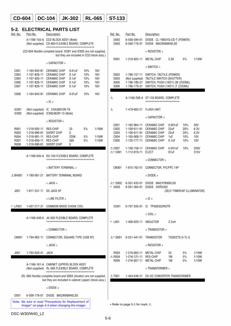
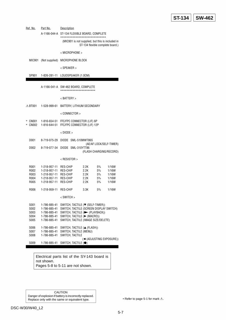
DSC-W30/W40_L2
CD-604 DC-104 JK-302 RL-065 ST-133
A-1166-155-A CCD BLOCK ASSY (Note)(Not supplied) CD-604 FLEXIBLE BOARD, COMPLETE
*******************************(CD-604 flexible complete board, IC001 and IC002 are not supplied,
but they are included in CCD block assy.)
< CAPACITOR >
C001 1-164-943-81 CERAMIC CHIP 0.01uF 10% 16VC003 1-107-826-11 CERAMIC CHIP 0.1uF 10% 16VC004 1-107-826-11 CERAMIC CHIP 0.1uF 10% 16VC006 1-107-826-11 CERAMIC CHIP 0.1uF 10% 16VC007 1-107-826-11 CERAMIC CHIP 0.1uF 10% 16V
C008 1-164-943-81 CERAMIC CHIP 0.01uF 10% 16V
< IC >
IC001 (Not supplied) IC CXA3691EN-T9IC002 (Not supplied) ICX624EQP-13 (Note)
< RESISTOR >
R001 1-218-935-11 RES-CHIP 33 5% 1/16WR002 1-218-990-81 SHORT CHIP 0R004 1-218-981-11 RES-CHIP 220K 5% 1/16WR007 1-218-950-11 RES-CHIP 560 5% 1/16WR008 1-218-990-81 SHORT CHIP 0
A-1166-045-A DC-104 FLEXIBLE BOARD, COMPLETE*******************************
< BATTERY TERMINAL >
0BH001 1-780-061-21 BATTERY TERMINAL BOARD
< JACK >
J001 1-817-331-11 DC JACK 5P
< LINE FILTER >
* LF001 1-457-217-21 COMMON MODE CHOKE COIL
A-1166-048-A JK-302 FLEXIBLE BOARD, COMPLETE******************************
< CONNECTOR >
CN001 1-794-962-11 CONNECTOR, SQUARE TYPE (USB 5P)
< JACK >
J001 1-793-620-41 JACK
A-1166-161-A CABINET (UPPER) BLOCK ASSY(Not supplied) RL-065 FLEXIBLE BOARD, COMPLETE
*******************************(RL-065 flexible complete board and S003 (shutter) are not supplied,
but they are included in cabinet (upper) block assy.)
< DIODE >
D001 6-500-776-01 DIODE MAZW068H0LS0
D002 6-500-594-01 DIODE CL-196SYG-CD-T (POWER)D003 6-500-776-01 DIODE MAZW068H0LS0
< RESISTOR >
R001 1-216-825-11 METAL CHIP 2.2K 5% 1/10W
< SWITCH >
S002 1-786-157-11 SWITCH, TACTILE (POWER)S003 (Not supplied) TACTILE SWITCH (SHUTTER)S005 1-786-180-31 SWITCH, PUSH (1KEY) (W (ZOOM))S006 1-786-179-31 SWITCH, PUSH (1KEY) (T (ZOOM))
0 A-1166-208-A ST-133 BOARD, COMPLETE**********************
0 1-479-663-21 FLASH UNIT
< CAPACITOR >
C001 1-162-964-11 CERAMIC CHIP 0.001uF 10% 50VC002 1-100-611-91 CERAMIC CHIP 22uF 20% 6.3VC003 1-100-611-91 CERAMIC CHIP 22uF 20% 6.3VC004 1-165-908-11 CERAMIC CHIP 1uF 10% 10VC005 1-125-777-11 CERAMIC CHIP 0.1uF 10% 10V
0C007 1-100-758-11 CERAMIC CHIP 0.047uF 10% 250V0* C901 1-112-819-11 ELECT 97uF 315V
< CONNECTOR >
CN001 1-815-762-51 CONNECTOR, FFC/FPC 14P
< DIODE >
0* D002 6-501-433-01 DIODE MA2YF8000LS0* D003 6-501-364-01 DIODE DOR5352
(SELF-TIMER/AF ILLUMINATOR)
< IC >
IC001 6-707-555-01 IC TPS65552RGTR
< COIL >
* L001 1-400-820-11 INDUCTOR 2.2uH
< TRANSISTOR >
0* Q001 6-551-447-01 TRANSISTOR TIG022TS-S-TL-E
< RESISTOR >
R003 1-216-803-11 METAL CHIP 33 5% 1/10W0R004 1-216-121-11 RES-CHIP 1M 5% 1/10W
R005 1-216-857-11 METAL CHIP 1M 5% 1/10W
< TRANSFORMER >
0T001 1-443-648-21 DC-DC CONVERTER TRANSFORMER
Note: Be sure to read “Precautions for Replacement ofImager” on page 4-3 when changing the imager. • Refer to page 5-1 for mark 0.
5-7
Ref. No. Part No. Description Ref. No. Part No. Description
DSC-W30/W40_L2
ST-134 SW-462
A-1166-044-A ST-134 FLEXIBLE BOARD, COMPLETE******************************
(MIC901 is not supplied, but this is included inST-134 flexible complete board.)
< MICROPHONE >
MIC901 (Not supplied) MICROPHONE BLOCK
< SPEAKER >
SP901 1-826-281-11 LOUDSPEAKER (1.0CM)
A-1166-041-A SW-462 BOARD, COMPLETE***********************
< BATTERY >
0BT001 1-528-999-61 BATTERY, LITHIUM SECONDARY
< CONNECTOR >
* CN001 1-816-654-51 FFC/FPC CONNECTOR (LIF) 6P* CN002 1-816-644-51 FFC/FPC CONNECTOR (LIF) 12P
< DIODE >
D001 8-719-075-29 DIODE SML-510MWT86S(AE/AF LOCK/SELF-TIMER)
D002 8-719-077-34 DIODE SML-310YTT86(FLASH CHARGING/RECORD)
< RESISTOR >
R001 1-218-957-11 RES-CHIP 2.2K 5% 1/16WR002 1-218-957-11 RES-CHIP 2.2K 5% 1/16WR003 1-218-957-11 RES-CHIP 2.2K 5% 1/16WR004 1-218-957-11 RES-CHIP 2.2K 5% 1/16WR005 1-218-957-11 RES-CHIP 2.2K 5% 1/16W
R006 1-218-959-11 RES-CHIP 3.3K 5% 1/16W
< SWITCH >
S001 1-786-885-41 SWITCH, TACTILE (V (SELF-TIMER))S002 1-786-885-41 SWITCH, TACTILE (SCREEN DISPLAY SWITCH)S003 1-786-885-41 SWITCH, TACTILE (N (PLAYBACK))S004 1-786-885-41 SWITCH, TACTILE (B (MACRO))S005 1-786-885-41 SWITCH, TACTILE (IMAGE SIZE/DELETE)
S006 1-786-885-41 SWITCH, TACTILE (v (FLASH))S007 1-786-885-41 SWITCH, TACTILE (MENU)S008 1-786-885-41 SWITCH, TACTILE
(b (ADJUSTING EXPOSURE))S009 1-786-885-41 SWITCH, TACTILE (z)
CAUTIONDanger of explosion if battery is incorrectly replaced.Replace only with the same or equivalent type. • Refer to page 5-1 for mark 0.
Electrical parts list of the SY-143 board isnot shown.Pages 5-8 to 5-11 are not shown.
DSC-W30/W40_L25-12E
• Refer to the page 5-1 for mark 0.
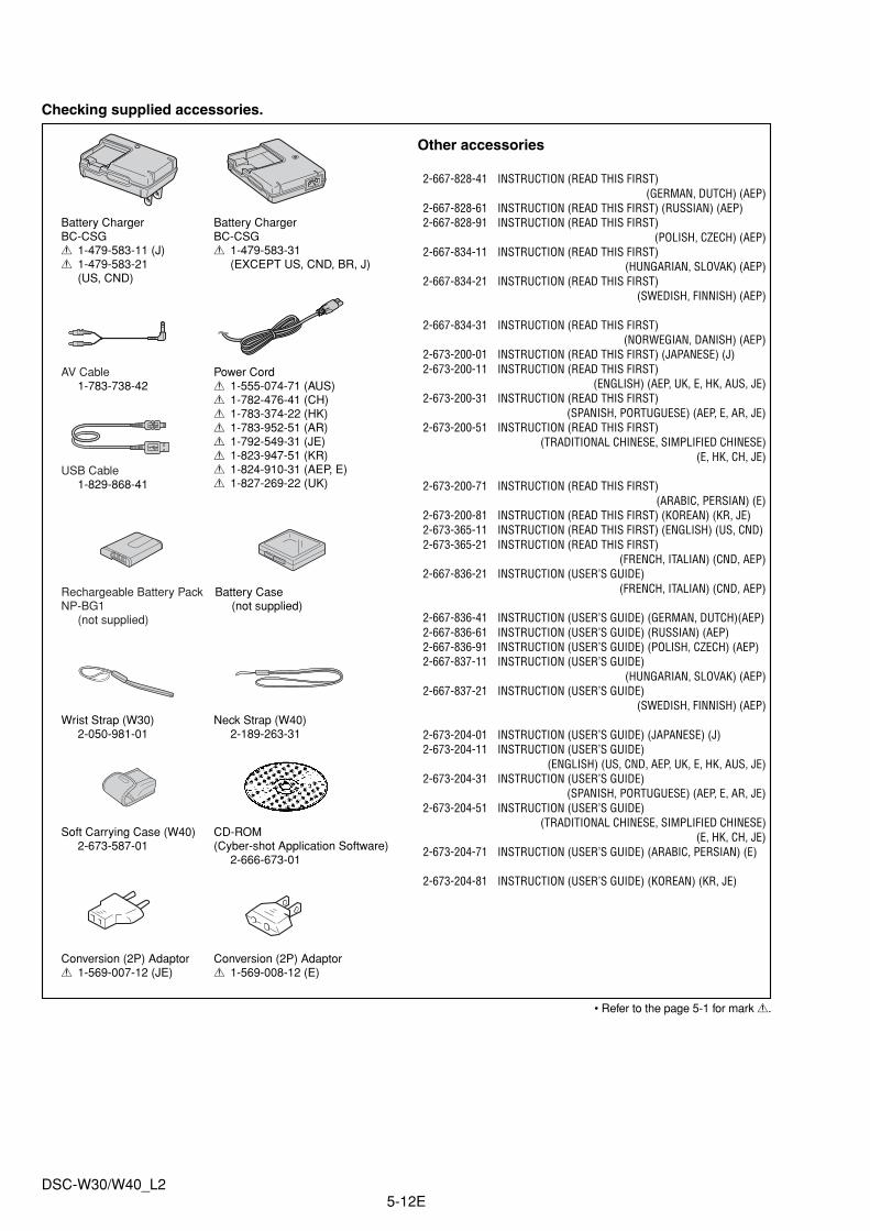
Checking supplied accessories.
Other accessories
2-667-828-41 INSTRUCTION (READ THIS FIRST)(GERMAN, DUTCH) (AEP)
2-667-828-61 INSTRUCTION (READ THIS FIRST) (RUSSIAN) (AEP)2-667-828-91 INSTRUCTION (READ THIS FIRST)
(POLISH, CZECH) (AEP)2-667-834-11 INSTRUCTION (READ THIS FIRST)
(HUNGARIAN, SLOVAK) (AEP)2-667-834-21 INSTRUCTION (READ THIS FIRST)
(SWEDISH, FINNISH) (AEP)
2-667-834-31 INSTRUCTION (READ THIS FIRST)(NORWEGIAN, DANISH) (AEP)
2-673-200-01 INSTRUCTION (READ THIS FIRST) (JAPANESE) (J)2-673-200-11 INSTRUCTION (READ THIS FIRST)
(ENGLISH) (AEP, UK, E, HK, AUS, JE)2-673-200-31 INSTRUCTION (READ THIS FIRST)
(SPANISH, PORTUGUESE) (AEP, E, AR, JE)2-673-200-51 INSTRUCTION (READ THIS FIRST)
(TRADITIONAL CHINESE, SIMPLIFIED CHINESE) (E, HK, CH, JE)
2-673-200-71 INSTRUCTION (READ THIS FIRST)(ARABIC, PERSIAN) (E)
2-673-200-81 INSTRUCTION (READ THIS FIRST) (KOREAN) (KR, JE)2-673-365-11 INSTRUCTION (READ THIS FIRST) (ENGLISH) (US, CND)2-673-365-21 INSTRUCTION (READ THIS FIRST)
(FRENCH, ITALIAN) (CND, AEP)2-667-836-21 INSTRUCTION (USER’S GUIDE)
(FRENCH, ITALIAN) (CND, AEP)
2-667-836-41 INSTRUCTION (USER’S GUIDE) (GERMAN, DUTCH)(AEP)2-667-836-61 INSTRUCTION (USER’S GUIDE) (RUSSIAN) (AEP)2-667-836-91 INSTRUCTION (USER’S GUIDE) (POLISH, CZECH) (AEP)2-667-837-11 INSTRUCTION (USER’S GUIDE)
(HUNGARIAN, SLOVAK) (AEP)2-667-837-21 INSTRUCTION (USER’S GUIDE)
(SWEDISH, FINNISH) (AEP)
2-673-204-01 INSTRUCTION (USER’S GUIDE) (JAPANESE) (J)2-673-204-11 INSTRUCTION (USER’S GUIDE)
(ENGLISH) (US, CND, AEP, UK, E, HK, AUS, JE)2-673-204-31 INSTRUCTION (USER’S GUIDE)
(SPANISH, PORTUGUESE) (AEP, E, AR, JE)2-673-204-51 INSTRUCTION (USER’S GUIDE)
(TRADITIONAL CHINESE, SIMPLIFIED CHINESE)(E, HK, CH, JE)
2-673-204-71 INSTRUCTION (USER’S GUIDE) (ARABIC, PERSIAN) (E)
2-673-204-81 INSTRUCTION (USER’S GUIDE) (KOREAN) (KR, JE)
Battery ChargerBC-CSG0 1-479-583-11 (J)0 1-479-583-21
(US, CND)
Battery ChargerBC-CSG0 1-479-583-31
(EXCEPT US, CND, BR, J)
Power Cord0 1-555-074-71 (AUS)0 1-782-476-41 (CH)0 1-783-374-22 (HK)0 1-783-952-51 (AR)0 1-792-549-31 (JE)0 1-823-947-51 (KR)0 1-824-910-31 (AEP, E)0 1-827-269-22 (UK)
Conversion (2P) Adaptor0 1-569-007-12 (JE)
Conversion (2P) Adaptor0 1-569-008-12 (E)
Battery Case(not supplied)
Rechargeable Battery Pack NP-BG1
(not supplied)
CD-ROM(Cyber-shot Application Software)
2-666-673-01
Soft Carrying Case (W40)2-673-587-01
AV Cable1-783-738-42
USB Cable1-829-868-41
Wrist Strap (W30)2-050-981-01
Neck Strap (W40)2-189-263-31
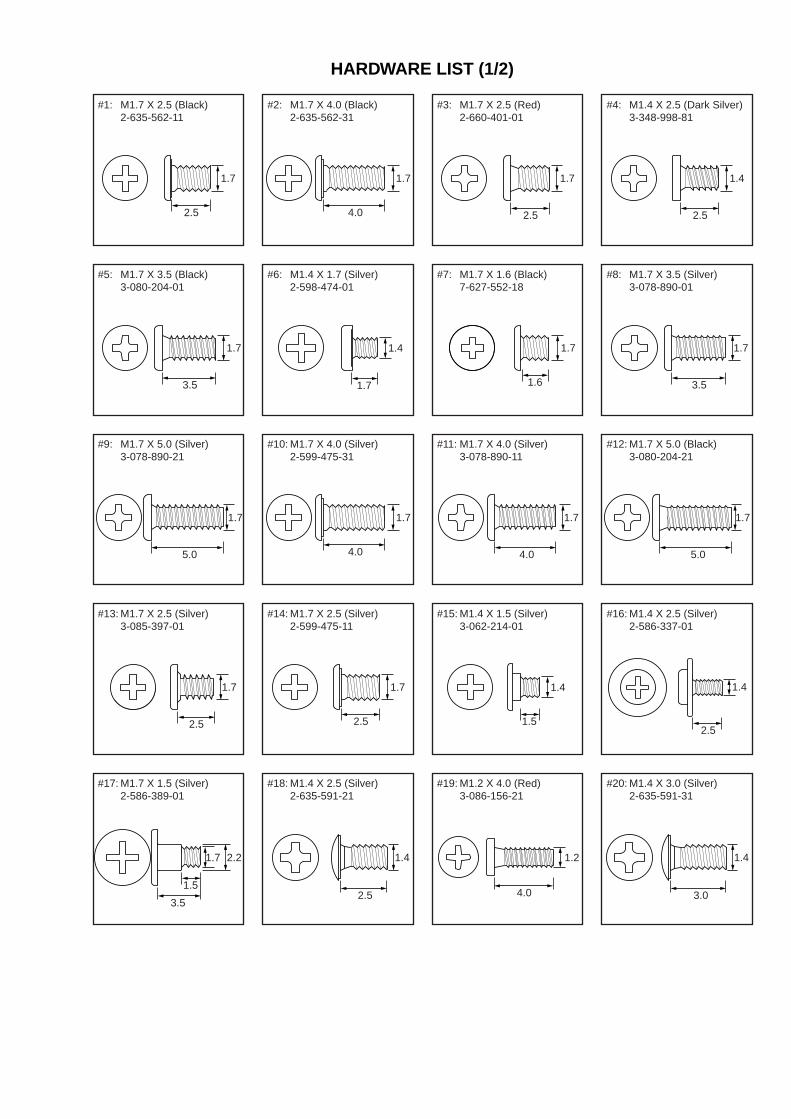
#1: M1.7 X 2.5 (Black)2-635-562-11
2.5
1.7
#10: M1.7 X 4.0 (Silver)2-599-475-31
1.6
1.7
#6: M1.4 X 1.7 (Silver)2-598-474-01
1.7
1.4
#7: M1.7 X 1.6 (Black)7-627-552-18
#3: M1.7 X 2.5 (Red)2-660-401-01
2.5
1.7
#2: M1.7 X 4.0 (Black)2-635-562-31
4.0
1.7
4.0
1.7
#5: M1.7 X 3.5 (Black)3-080-204-01
3.5
1.7
#4: M1.4 X 2.5 (Dark Silver)3-348-998-81
2.5
1.4
#12: M1.7 X 5.0 (Black)3-080-204-21
1.7
#9: M1.7 X 5.0 (Silver)3-078-890-21
5.0
1.7
#14: M1.7 X 2.5 (Silver)2-599-475-11
#13: M1.7 X 2.5 (Silver)3-085-397-01
2.5
1.7
#11: M1.7 X 4.0 (Silver)3-078-890-11
#8: M1.7 X 3.5 (Silver)3-078-890-01
3.5
1.7
4.0
1.7
5.0
2.5
#17: M1.7 X 1.5 (Silver)2-586-389-01
2.5
1.7
#15: M1.4 X 1.5 (Silver)3-062-214-01
1.5
1.4 1.4
#16: M1.4 X 2.5 (Silver)2-586-337-01
1.5
3.5
1.7 2.2
#18: M1.4 X 2.5 (Silver)2-635-591-21
2.5
1.4
#19: M1.2 X 4.0 (Red)3-086-156-21
4.0
1.2
#20: M1.4 X 3.0 (Silver)2-635-591-31
3.0
1.4
HARDWARE LIST (1/2)

HARDWARE LIST (2/2)
#21: M1.4 X 3.0 (Black)2-662-396-21
3.0
1.4
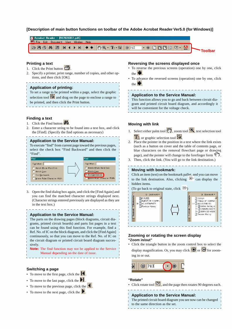
[Description of main button functions on toolbar of the Adobe Acrobat Reader Ver5.0 (for Windows)]
Printing a text1. Click the Print button .2. Specify a printer, print range, number of copies, and other op-
tions, and then click [OK].
Application of printing:To set a range to be printed within a page, select the graphic
selection tool and drag on the page to enclose a range tobe printed, and then click the Print button.
Finding a text1. Click the Find button .2. Enter a character string to be found into a text box, and click
the [Find]. (Specify the find options as necessary)
Application to the Service Manual:To execute “find” from current page toward the previous pages,select the check box “Find Backward” and then click the“Find”.
3. Open the find dialog box again, and click the [Find Again] andyou can find the matched character strings displayed next.(Character strings entered previously are displayed as they arein the text box.)
Application to the Service Manual:The parts on the drawing pages (block diagrams, circuit dia-grams, printed circuit boards) and parts list pages in a textcan be found using this find function. For example, find aRef. No. of IC on the block diagram, and click the [Find Again]continuously, so that you can move to the Ref. No. of IC onthe circuit diagram or printed circuit board diagram succes-sively.Note: The find function may not be applied to the Service
Manual depending on the date of issue.
Switching a page• To move to the first page, click the .
• To move to the last page, click the .
• To move to the previous page, click the .
• To move to the next page, click the .
Reversing the screens displayed once• To reverse the previous screens (operation) one by one, click
the .
• To advance the reversed screens (operation) one by one, click
the .
Application to the Service Manual:This function allows you to go and back between circuit dia-gram and printed circuit board diagram, and accordingly itwill be convenient for the voltage check.
Moving with link
1. Select either palm tool , zoom tool , text selection tool
, or graphic selection tool .2. Place the pointer in the position in a text where the link exists
(such as a button on cover and the table of contents page, orblue characters on the removal flowchart page or drawingpage), and the pointer will change to the forefinger form .
3. Then, click the link. (You will go to the link destination.)
Moving with bookmark:Click an item (text) on the bookmark pallet, and you can moveto the link destination. Also, clicking can display thehidden items.(To go back to original state, click )
Zooming or rotating the screen display“Zoom in/out”• Click the triangle button in the zoom control box to select the
display magnification. Or, you may click or for zoom-
ing in or out.
“Rotate”• Click rotate tool , and the page then rotates 90 degrees each.
Application to the Service Manual:The printed circuit board diagram you see now can be changedto the same direction as the set.
Toolbar
Revision History
Reverse
DSC-W30/W40_L2
Ver.
1.0
Date
2006.01
History
Official Release
Contents
—
S.M. Rev.issued
—
987693531.pdf