Embed Size (px)
Citation preview
ReceiverDriverDIN1
DOUT1+
DSLVDS1047
ReceiverDriver
ReceiverDriver
ReceiverDriver
DIN2
DIN3
DIN4
DSLVDS1048
DOUT2+
DOUT3+
DOUT4+
DOUT1-
DOUT2-
DOUT3-
DOUT4-
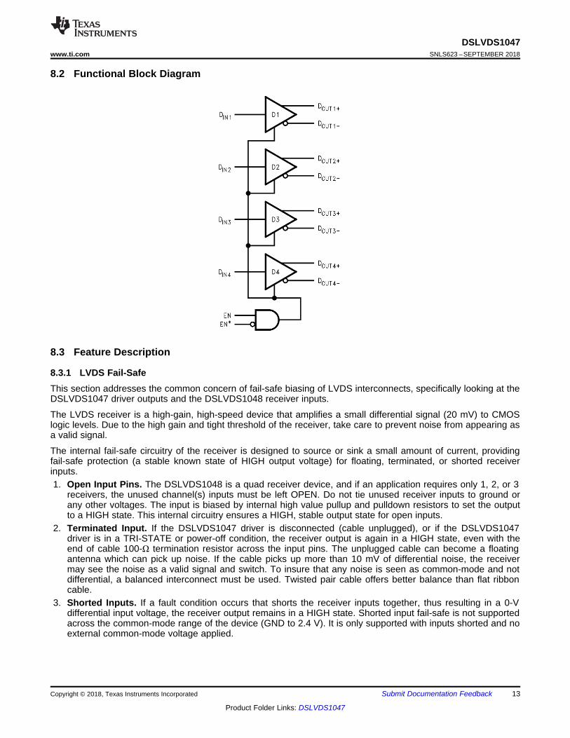
EN
EN*
RIN1+
RIN1-
RIN2+
RIN2-
RIN3+
RIN3-
RIN4+
RIN4-
ROUT1
ROUT2
ROUT3
ROUT4
100 100
100
EN
EN*
100
Product
Folder
Order
Now
Technical
Documents
Tools &
Software
Support &Community
An IMPORTANT NOTICE at the end of this data sheet addresses availability, warranty, changes, use in safety-critical applications,intellectual property matters and other important disclaimers. PRODUCTION DATA.
DSLVDS1047SNLS623 –SEPTEMBER 2018
DSLVDS1047 3.3-V LVDS Quad Channel High-Speed Differential Line Driver
1
1 Features1• Designed for Signaling Rates up to 400-Mbps• 3.3-V Power Supply Design• 300-ps Typical Differential Skew• 400-ps Maximum Differential Skew• 1.7-ns Maximum Propagation Delay• ±350-mV Differential Signaling• Low Power Dissipation (13 mW at 3.3-V Static)• Interoperable With Existing 5-V LVDS Receivers• High impedance on LVDS Outputs on Power
Down• Flow-Through Pinout Simplifies PCB Layout• Meets or Exceeds TIA/EIA-644 LVDS Standard• Industrial Operating Temperature Range
(−40°C to +85°C)• Available in TSSOP Package
2 Applications• Multifunction Printers• Board-to-Board Communication• Test and Measurement• Printers• Data Center Interconnect• Lab Instrumentation• Ultrasound Scanners
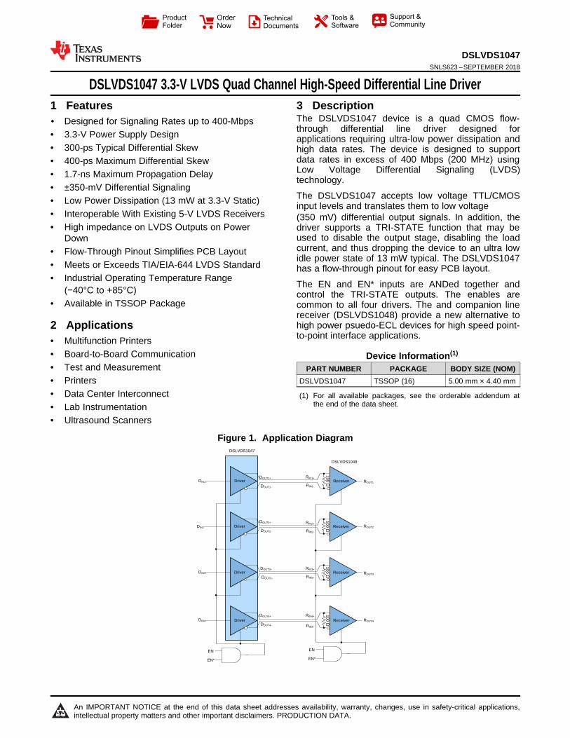
3 DescriptionThe DSLVDS1047 device is a quad CMOS flow-through differential line driver designed forapplications requiring ultra-low power dissipation andhigh data rates. The device is designed to supportdata rates in excess of 400 Mbps (200 MHz) usingLow Voltage Differential Signaling (LVDS)technology.
The DSLVDS1047 accepts low voltage TTL/CMOSinput levels and translates them to low voltage(350 mV) differential output signals. In addition, thedriver supports a TRI-STATE function that may beused to disable the output stage, disabling the loadcurrent, and thus dropping the device to an ultra lowidle power state of 13 mW typical. The DSLVDS1047has a flow-through pinout for easy PCB layout.
The EN and EN* inputs are ANDed together andcontrol the TRI-STATE outputs. The enables arecommon to all four drivers. The and companion linereceiver (DSLVDS1048) provide a new alternative tohigh power psuedo-ECL devices for high speed point-to-point interface applications.
Device Information(1)
PART NUMBER PACKAGE BODY SIZE (NOM)DSLVDS1047 TSSOP (16) 5.00 mm × 4.40 mm
(1) For all available packages, see the orderable addendum atthe end of the data sheet.
Figure 1. Application Diagram
2
DSLVDS1047SNLS623 –SEPTEMBER 2018 www.ti.com
Product Folder Links: DSLVDS1047
Submit Documentation Feedback Copyright © 2018, Texas Instruments Incorporated
Table of Contents1 Features .................................................................. 12 Applications ........................................................... 13 Description ............................................................. 14 Revision History..................................................... 25 Pin Configuration and Functions ......................... 36 Specifications......................................................... 4
6.1 Absolute Maximum Ratings ...................................... 46.2 ESD Ratings.............................................................. 46.3 Recommended Operating Conditions....................... 46.4 Thermal Information .................................................. 46.5 Electrical Characteristics .......................................... 56.6 Switching Characteristics ......................................... 66.7 Typical Characteristics .............................................. 7
7 Parameter Measurement Information .................. 98 Detailed Description ............................................ 12
8.1 Overview ................................................................. 128.2 Functional Block Diagram ....................................... 13
8.3 Feature Description................................................. 138.4 Device Functional Modes........................................ 14
9 Application and Implementation ........................ 159.1 Application Information............................................ 159.2 Typical Application ................................................. 15
10 Power Supply Recommendations ..................... 1811 Layout................................................................... 18
11.1 Layout Guidelines ................................................. 1811.2 Layout Example .................................................... 19
12 Device and Documentation Support ................. 2012.1 Receiving Notification of Documentation Updates 2012.2 Community Resources.......................................... 2012.3 Trademarks ........................................................... 2012.4 Electrostatic Discharge Caution............................ 2012.5 Glossary ................................................................ 20
13 Mechanical, Packaging, and OrderableInformation ........................................................... 21
4 Revision HistoryNOTE: Page numbers for previous revisions may differ from page numbers in the current version.
DATE REVISION NOTESSeptember 2018 * Initial release.
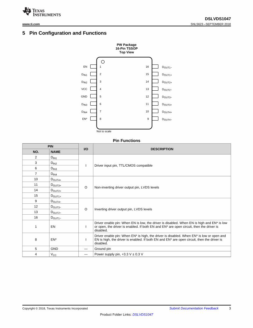
1EN 16 DOUT1í
2DIN1 15 DOUT1+
3DIN2 14 DOUT2+
4VCC 13 DOUT2í�
5GND 12 DOUT3í
6DIN3 11 DOUT3+
7DIN4 10 DOUT4+
8EN* 9 DOUT4í�
Not to scale
3
DSLVDS1047www.ti.com SNLS623 –SEPTEMBER 2018
Product Folder Links: DSLVDS1047
Submit Documentation FeedbackCopyright © 2018, Texas Instruments Incorporated
5 Pin Configuration and Functions
PW Package16-Pin TSSOP
Top View
Pin FunctionsPIN
I/O DESCRIPTIONNO. NAME
2 DIN1
I Driver input pin, TTL/CMOS compatible3 DIN2
6 DIN3
7 DIN4
10 DOUT4+
O Non-inverting driver output pin, LVDS levels11 DOUT3+
14 DOUT2+
15 DOUT1+
9 DOUT4−
O Inverting driver output pin, LVDS levels12 DOUT3−
13 DOUT2−
16 DOUT1−
1 EN IDriver enable pin: When EN is low, the driver is disabled. When EN is high and EN* is lowor open, the driver is enabled. If both EN and EN* are open circuit, then the driver isdisabled.
8 EN* IDriver enable pin: When EN* is high, the driver is disabled. When EN* is low or open andEN is high, the driver is enabled. If both EN and EN* are open circuit, then the driver isdisabled.
5 GND — Ground pin4 VCC — Power supply pin, +3.3 V ± 0.3 V
4
DSLVDS1047SNLS623 –SEPTEMBER 2018 www.ti.com
Product Folder Links: DSLVDS1047
Submit Documentation Feedback Copyright © 2018, Texas Instruments Incorporated
(1) Stresses beyond those listed under Absolute Maximum Ratings may cause permanent damage to the device. These are stress ratingsonly, which do not imply functional operation of the device at these or any other conditions beyond those indicated under RecommendedOperating Conditions. Exposure to absolute-maximum-rated conditions for extended periods may affect device reliability.
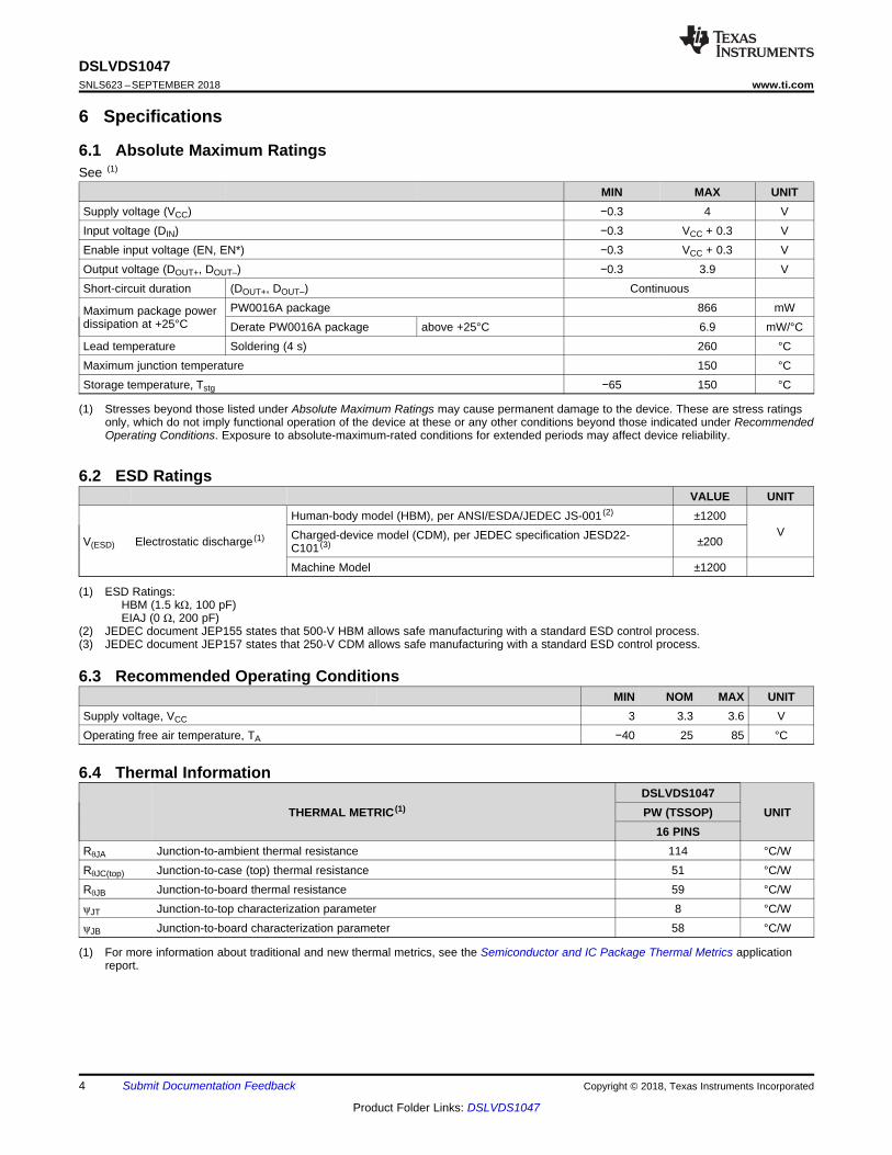
6 Specifications
6.1 Absolute Maximum RatingsSee (1)
MIN MAX UNITSupply voltage (VCC) −0.3 4 VInput voltage (DIN) −0.3 VCC + 0.3 VEnable input voltage (EN, EN*) −0.3 VCC + 0.3 VOutput voltage (DOUT+, DOUT–) −0.3 3.9 VShort-circuit duration (DOUT+, DOUT–) Continuous
Maximum package powerdissipation at +25°C
PW0016A package 866 mWDerate PW0016A package above +25°C 6.9 mW/°C
Lead temperature Soldering (4 s) 260 °CMaximum junction temperature 150 °CStorage temperature, Tstg −65 150 °C
(1) ESD Ratings:HBM (1.5 kΩ, 100 pF)EIAJ (0 Ω, 200 pF)
(2) JEDEC document JEP155 states that 500-V HBM allows safe manufacturing with a standard ESD control process.(3) JEDEC document JEP157 states that 250-V CDM allows safe manufacturing with a standard ESD control process.
6.2 ESD RatingsVALUE UNIT
V(ESD) Electrostatic discharge (1)
Human-body model (HBM), per ANSI/ESDA/JEDEC JS-001 (2) ±1200VCharged-device model (CDM), per JEDEC specification JESD22-
C101 (3) ±200
Machine Model ±1200
6.3 Recommended Operating ConditionsMIN NOM MAX UNIT
Supply voltage, VCC 3 3.3 3.6 VOperating free air temperature, TA −40 25 85 °C
(1) For more information about traditional and new thermal metrics, see the Semiconductor and IC Package Thermal Metrics applicationreport.
6.4 Thermal Information
THERMAL METRIC (1)DSLVDS1047
UNITPW (TSSOP)16 PINS
RθJA Junction-to-ambient thermal resistance 114 °C/WRθJC(top) Junction-to-case (top) thermal resistance 51 °C/WRθJB Junction-to-board thermal resistance 59 °C/WψJT Junction-to-top characterization parameter 8 °C/WψJB Junction-to-board characterization parameter 58 °C/W
5
DSLVDS1047www.ti.com SNLS623 –SEPTEMBER 2018
Product Folder Links: DSLVDS1047
Submit Documentation FeedbackCopyright © 2018, Texas Instruments Incorporated
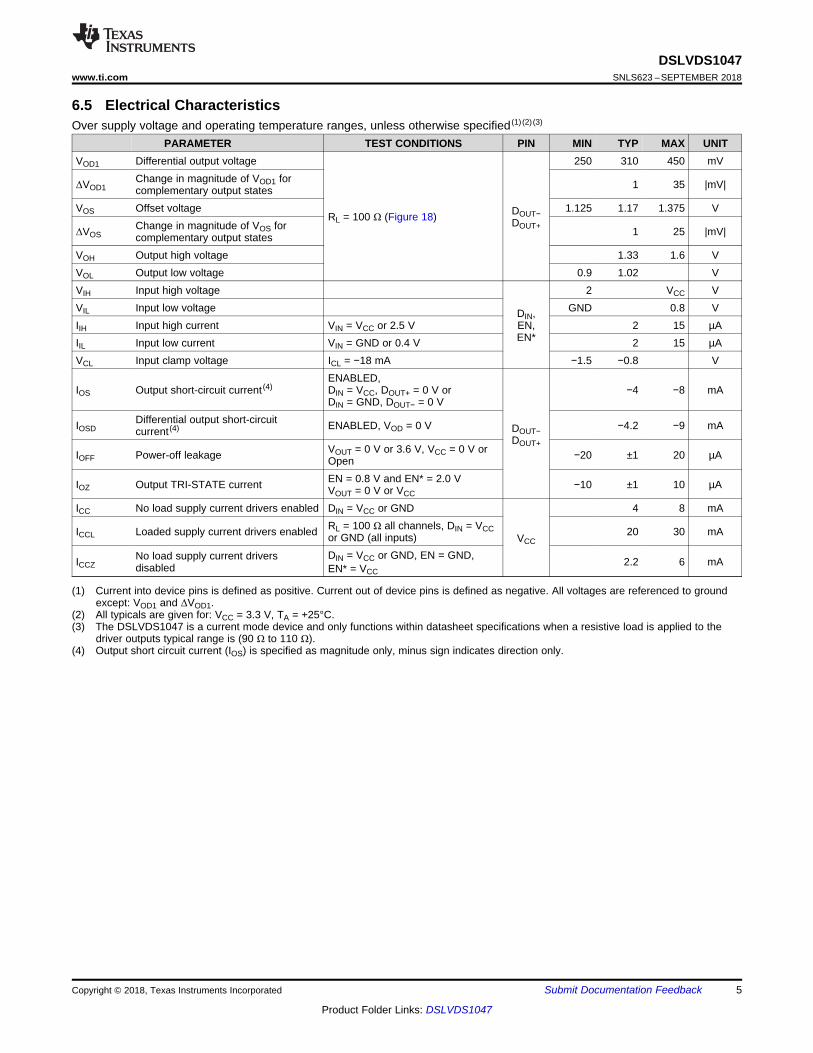
(1) Current into device pins is defined as positive. Current out of device pins is defined as negative. All voltages are referenced to groundexcept: VOD1 and ΔVOD1.
(2) All typicals are given for: VCC = 3.3 V, TA = +25°C.(3) The DSLVDS1047 is a current mode device and only functions within datasheet specifications when a resistive load is applied to the
driver outputs typical range is (90 Ω to 110 Ω).(4) Output short circuit current (IOS) is specified as magnitude only, minus sign indicates direction only.
6.5 Electrical CharacteristicsOver supply voltage and operating temperature ranges, unless otherwise specified (1) (2) (3)
PARAMETER TEST CONDITIONS PIN MIN TYP MAX UNITVOD1 Differential output voltage
RL = 100 Ω (Figure 18) DOUT−DOUT+
250 310 450 mV
ΔVOD1Change in magnitude of VOD1 forcomplementary output states 1 35 |mV|
VOS Offset voltage 1.125 1.17 1.375 V
ΔVOSChange in magnitude of VOS forcomplementary output states 1 25 |mV|
VOH Output high voltage 1.33 1.6 VVOL Output low voltage 0.9 1.02 VVIH Input high voltage
DIN,EN,EN*
2 VCC VVIL Input low voltage GND 0.8 VIIH Input high current VIN = VCC or 2.5 V 2 15 µAIIL Input low current VIN = GND or 0.4 V 2 15 µAVCL Input clamp voltage ICL = −18 mA −1.5 −0.8 V
IOS Output short-circuit current (4)ENABLED,DIN = VCC, DOUT+ = 0 V orDIN = GND, DOUT− = 0 V
DOUT−DOUT+
−4 −8 mA
IOSDDifferential output short-circuitcurrent (4) ENABLED, VOD = 0 V −4.2 −9 mA
IOFF Power-off leakage VOUT = 0 V or 3.6 V, VCC = 0 V orOpen −20 ±1 20 µA
IOZ Output TRI-STATE current EN = 0.8 V and EN* = 2.0 VVOUT = 0 V or VCC
−10 ±1 10 µA
ICC No load supply current drivers enabled DIN = VCC or GND
VCC
4 8 mA
ICCL Loaded supply current drivers enabled RL = 100 Ω all channels, DIN = VCCor GND (all inputs) 20 30 mA
ICCZNo load supply current driversdisabled
DIN = VCC or GND, EN = GND,EN* = VCC
2.2 6 mA
6
DSLVDS1047SNLS623 –SEPTEMBER 2018 www.ti.com
Product Folder Links: DSLVDS1047
Submit Documentation Feedback Copyright © 2018, Texas Instruments Incorporated
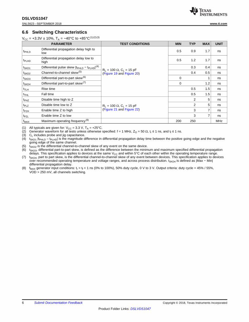
(1) All typicals are given for: VCC = 3.3 V, TA = +25°C.(2) Generator waveform for all tests unless otherwise specified: f = 1 MHz, ZO = 50 Ω, tr ≤ 1 ns, and tf ≤ 1 ns.(3) CL includes probe and jig capacitance.(4) tSKD1 |tPHLD – tPLHD| is the magnitude difference in differential propagation delay time between the positive going edge and the negative
going edge of the same channel.(5) tSKD2 is the differential channel-to-channel skew of any event on the same device.(6) tSKD3, differential part-to-part skew, is defined as the difference between the minimum and maximum specified differential propagation
delays. This specification applies to devices at the same VCC and within 5°C of each other within the operating temperature range.(7) tSKD4, part to part skew, is the differential channel-to-channel skew of any event between devices. This specification applies to devices
over recommended operating temperature and voltage ranges, and across process distribution. tSKD4 is defined as |Max − Min|differential propagation delay.
(8) fMAX generator input conditions: tr = tf < 1 ns (0% to 100%), 50% duty cycle, 0 V to 3 V. Output criteria: duty cycle = 45% / 55%,VOD > 250 mV, all channels switching.
6.6 Switching CharacteristicsVCC = +3.3V ± 10%, TA = −40°C to +85°C (1) (2) (3)
PARAMETER TEST CONDITIONS MIN TYP MAX UNIT
tPHLDDifferential propagation delay high tolow
RL = 100 Ω, CL = 15 pF(Figure 19 and Figure 20)
0.5 0.9 1.7 ns
tPLHDDifferential propagation delay low tohigh 0.5 1.2 1.7 ns
tSKD1 Differential pulse skew |tPHLD − tPLHD| (4) 0.3 0.4 nstSKD2 Channel-to-channel skew (5) 0.4 0.5 nstSKD3 Differential part-to-part skew (6) 0 1 nstSKD4 Differential part-to-part skew (7) 0 1.2 nstTLH Rise time 0.5 1.5 nstTHL Fall time 0.5 1.5 nstPHZ Disable time high to Z
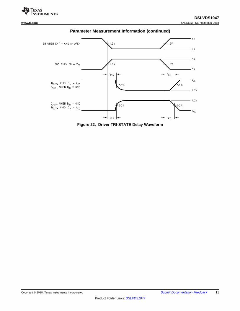
RL = 100 Ω, CL = 15 pF(Figure 21 and Figure 22)
2 5 nstPLZ Disable time low to Z 2 5 nstPZH Enable time Z to high 3 7 nstPZL Enable time Z to low 3 7 nsfMAX Maximum operating frequency (8) 200 250 MHz
7
DSLVDS1047www.ti.com SNLS623 –SEPTEMBER 2018
Product Folder Links: DSLVDS1047
Submit Documentation FeedbackCopyright © 2018, Texas Instruments Incorporated
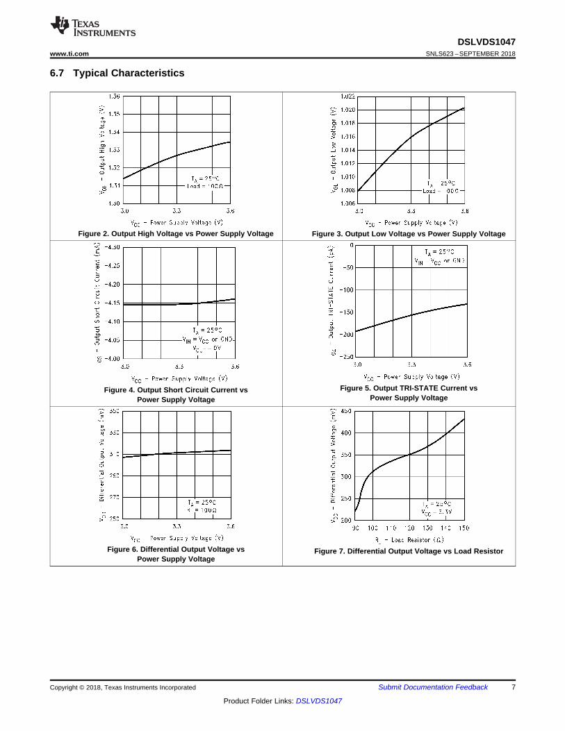
6.7 Typical Characteristics
Figure 2. Output High Voltage vs Power Supply Voltage Figure 3. Output Low Voltage vs Power Supply Voltage
Figure 4. Output Short Circuit Current vsPower Supply Voltage
Figure 5. Output TRI-STATE Current vsPower Supply Voltage
Figure 6. Differential Output Voltage vsPower Supply Voltage
Figure 7. Differential Output Voltage vs Load Resistor
8
DSLVDS1047SNLS623 –SEPTEMBER 2018 www.ti.com
Product Folder Links: DSLVDS1047
Submit Documentation Feedback Copyright © 2018, Texas Instruments Incorporated
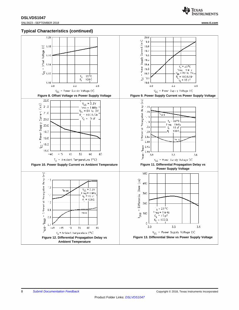
Typical Characteristics (continued)
Figure 8. Offset Voltage vs Power Supply Voltage Figure 9. Power Supply Current vs Power Supply Voltage
Figure 10. Power Supply Current vs Ambient Temperature Figure 11. Differential Propagation Delay vsPower Supply Voltage
Figure 12. Differential Propagation Delay vsAmbient Temperature
Figure 13. Differential Skew vs Power Supply Voltage
9
DSLVDS1047www.ti.com SNLS623 –SEPTEMBER 2018
Product Folder Links: DSLVDS1047
Submit Documentation FeedbackCopyright © 2018, Texas Instruments Incorporated
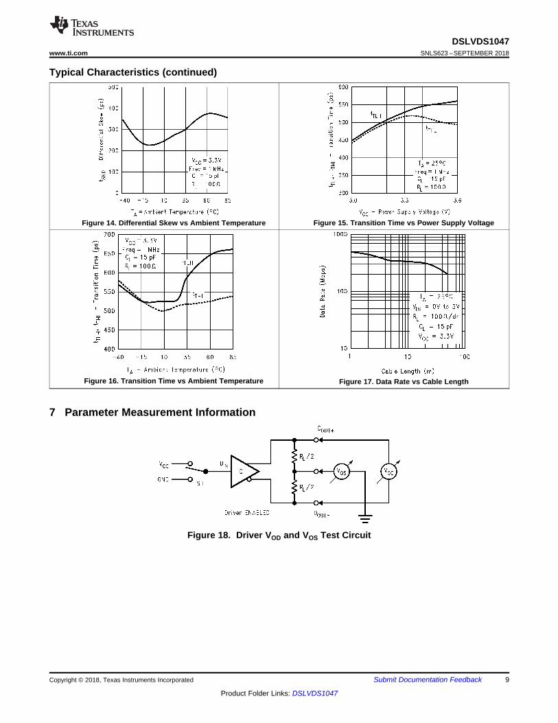
Typical Characteristics (continued)
Figure 14. Differential Skew vs Ambient Temperature Figure 15. Transition Time vs Power Supply Voltage
Figure 16. Transition Time vs Ambient Temperature Figure 17. Data Rate vs Cable Length
7 Parameter Measurement Information
Figure 18. Driver VOD and VOS Test Circuit
10
DSLVDS1047SNLS623 –SEPTEMBER 2018 www.ti.com
Product Folder Links: DSLVDS1047
Submit Documentation Feedback Copyright © 2018, Texas Instruments Incorporated
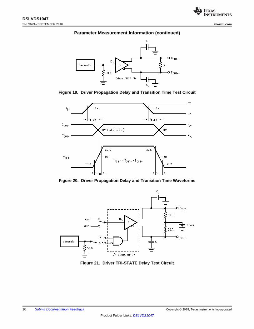
Parameter Measurement Information (continued)
Figure 19. Driver Propagation Delay and Transition Time Test Circuit
Figure 20. Driver Propagation Delay and Transition Time Waveforms
Figure 21. Driver TRI-STATE Delay Test Circuit
11
DSLVDS1047www.ti.com SNLS623 –SEPTEMBER 2018
Product Folder Links: DSLVDS1047
Submit Documentation FeedbackCopyright © 2018, Texas Instruments Incorporated
Parameter Measurement Information (continued)
Figure 22. Driver TRI-STATE Delay Waveform
12
DSLVDS1047SNLS623 –SEPTEMBER 2018 www.ti.com
Product Folder Links: DSLVDS1047
Submit Documentation Feedback Copyright © 2018, Texas Instruments Incorporated
8 Detailed Description
8.1 OverviewLVDS drivers and receivers are intended to be primarily used in an uncomplicated point-to-point configuration asis shown in Figure 24. This configuration provides a clean signaling environment for the fast edge rates of thedrivers. The receiver is connected to the driver through a balanced media which may be a standard twisted paircable, a parallel pair cable, or simply PCB traces. Typically, the characteristic differential impedance of the mediais in the range of 100 Ω. A termination resistor of 100 Ω (selected to match the media), and is located as close tothe receiver input pins as possible. The termination resistor converts the driver output current (current mode) intoa voltage that is detected by the receiver. Other configurations are possible such as a multi-receiverconfiguration, but the effects of a mid-stream connector(s), cable stub(s), and other impedance discontinuities aswell as ground shifting, noise margin limits, and total termination loading must be taken into account.
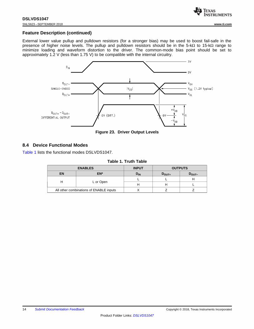
The DSLVDS1047 differential line driver is a balanced current source design. A current mode driver, generallyspeaking has a high output impedance and supplies a constant current for a range of loads (a voltage modedriver on the other hand supplies a constant voltage for a range of loads). Current is switched through the load inone direction to produce a logic state and in the other direction to produce the other logic state. The outputcurrent is typically 3.1 mA, a minimum of 2.5 mA, and a maximum of 4.5 mA. The current mode driver requiresthat a resistive termination be employed to terminate the signal and to complete the loop as shown in Figure 24.AC or unterminated configurations are not allowed. The 3.1-mA loop current develops a differential voltage of310 mV across the 100-Ω termination resistor which the receiver detects with a 250-mV minimum differentialnoise margin, (driven signal minus receiver threshold (250 mV – 100 mV = 150 mV). The signal is centeredaround +1.2 V (Driver Offset, VOS) with respect to ground as shown in Figure 23.
NOTEThe steady-state voltage (VSS) peak-to-peak swing is twice the differential voltage (VOD)and is typically 620 mV.
The current mode driver provides substantial benefits over voltage mode drivers, such as an RS-422 driver. Itsquiescent current remains relatively flat versus switching frequency. Whereas the RS-422 voltage mode driverincreases exponentially in most case from 20 MHz to 50 MHz. This is due to the overlap current that flowsbetween the rails of the device when the internal gates switch. Whereas the current mode driver switches a fixedcurrent between its output without any substantial overlap current. This is similar to some ECL and PECLdevices, but without the heavy static ICC requirements of the ECL/PECL designs. LVDS requires > 80% lesscurrent than similar PECL devices. AC specifications for the driver are a tenfold improvement over other existingRS-422 drivers.
The TRI-STATE function allows the driver outputs to be disabled, thus obtaining an even lower power state whenthe transmission of data is not required.
13
DSLVDS1047www.ti.com SNLS623 –SEPTEMBER 2018
Product Folder Links: DSLVDS1047
Submit Documentation FeedbackCopyright © 2018, Texas Instruments Incorporated
8.2 Functional Block Diagram
8.3 Feature Description
8.3.1 LVDS Fail-SafeThis section addresses the common concern of fail-safe biasing of LVDS interconnects, specifically looking at theDSLVDS1047 driver outputs and the DSLVDS1048 receiver inputs.
The LVDS receiver is a high-gain, high-speed device that amplifies a small differential signal (20 mV) to CMOSlogic levels. Due to the high gain and tight threshold of the receiver, take care to prevent noise from appearing asa valid signal.
The internal fail-safe circuitry of the receiver is designed to source or sink a small amount of current, providingfail-safe protection (a stable known state of HIGH output voltage) for floating, terminated, or shorted receiverinputs.1. Open Input Pins. The DSLVDS1048 is a quad receiver device, and if an application requires only 1, 2, or 3
receivers, the unused channel(s) inputs must be left OPEN. Do not tie unused receiver inputs to ground orany other voltages. The input is biased by internal high value pullup and pulldown resistors to set the outputto a HIGH state. This internal circuitry ensures a HIGH, stable output state for open inputs.
2. Terminated Input. If the DSLVDS1047 driver is disconnected (cable unplugged), or if the DSLVDS1047driver is in a TRI-STATE or power-off condition, the receiver output is again in a HIGH state, even with theend of cable 100-Ω termination resistor across the input pins. The unplugged cable can become a floatingantenna which can pick up noise. If the cable picks up more than 10 mV of differential noise, the receivermay see the noise as a valid signal and switch. To insure that any noise is seen as common-mode and notdifferential, a balanced interconnect must be used. Twisted pair cable offers better balance than flat ribboncable.
3. Shorted Inputs. If a fault condition occurs that shorts the receiver inputs together, thus resulting in a 0-Vdifferential input voltage, the receiver output remains in a HIGH state. Shorted input fail-safe is not supportedacross the common-mode range of the device (GND to 2.4 V). It is only supported with inputs shorted and noexternal common-mode voltage applied.
14
DSLVDS1047SNLS623 –SEPTEMBER 2018 www.ti.com
Product Folder Links: DSLVDS1047
Submit Documentation Feedback Copyright © 2018, Texas Instruments Incorporated
Feature Description (continued)External lower value pullup and pulldown resistors (for a stronger bias) may be used to boost fail-safe in thepresence of higher noise levels. The pullup and pulldown resistors should be in the 5-kΩ to 15-kΩ range tominimize loading and waveform distortion to the driver. The common-mode bias point should be set toapproximately 1.2 V (less than 1.75 V) to be compatible with the internal circuitry.
Figure 23. Driver Output Levels
8.4 Device Functional ModesTable 1 lists the functional modes DSLVDS1047.
Table 1. Truth TableENABLES INPUT OUTPUTS
EN EN* DIN DOUT+ DOUT−
H L or OpenL L HH H L
All other combinations of ENABLE inputs X Z Z

ReceiverDriverDIN1
DOUT1+
DSLVDS1047
ReceiverDriver
ReceiverDriver
ReceiverDriver
DIN2
DIN3
DIN4
DSLVDS1048
DOUT2+
DOUT3+
DOUT4+
DOUT1-
DOUT2-
DOUT3-
DOUT4-
EN
EN*
RIN1+
RIN1-
RIN2+
RIN2-
RIN3+
RIN3-
RIN4+
RIN4-
ROUT1
ROUT2
ROUT3
ROUT4
100 100
100
EN
EN*
100
15
DSLVDS1047www.ti.com SNLS623 –SEPTEMBER 2018
Product Folder Links: DSLVDS1047
Submit Documentation FeedbackCopyright © 2018, Texas Instruments Incorporated
9 Application and Implementation
NOTEInformation in the following applications sections is not part of the TI componentspecification, and TI does not warrant its accuracy or completeness. TI’s customers areresponsible for determining suitability of components for their purposes. Customers shouldvalidate and test their design implementation to confirm system functionality.
9.1 Application InformationThe DSLVDS1047 has a flow-through pinout that allows for easy PCB layout. The LVDS signals on one side ofthe device easily allows for matching electrical lengths of the differential pair trace lines between the driver andthe receiver as well as allowing the trace lines to be close together to couple noise as common-mode. Noiseisolation is achieved with the LVDS signals on one side of the device and the TTL signals on the other side.
9.2 Typical Application
Figure 24. Point-to-Point Application
16
DSLVDS1047SNLS623 –SEPTEMBER 2018 www.ti.com
Product Folder Links: DSLVDS1047
Submit Documentation Feedback Copyright © 2018, Texas Instruments Incorporated
Typical Application (continued)9.2.1 Design RequirementsWhen using LVDS devices, it is important to remember to specify controlled impedance PCB traces, cableassemblies, and connectors. All components of the transmission media should have a matched differentialimpedance of about 100 Ω. They should not introduce major impedance discontinuities.
Balanced cables (for example, twisted pair) are usually better than unbalanced cables (ribbon cable) for noisereduction and signal quality. Balanced cables tend to generate less EMI due to field canceling effects and alsotend to pick up electromagnetic radiation as common-mode (not differential mode) noise which is rejected by theLVDS receiver.
For cable distances < 0.5 M, most cables can be made to work effectively. For distances 0.5 M ≤ d ≤ 10 M,CAT5 (Category 5) twisted pair cable works well, is readily available and relatively inexpensive.
Table 2. Design RequirementsDESIGN PARAMETERS EXAMPLE VALUE
Driver Supply Voltage (VCC) 3.0 to 3.6 VDriver Input Voltage 0 to 3.6 V
Driver Signaling Rate DC to 400 MbpsInterconnect Characteristic Impedance 100 Ω
Termination Resistance 100 Ω
Number of Receiver Nodes 1Ground shift between driver and receiver ±1 V
9.2.2 Detailed Design Procedure
9.2.2.1 Probing LVDS Transmission LinesAlways use high impedance (> 100 kΩ), low capacitance (< 2 pF) scope probes with a wide bandwidth (1 GHz)scope. Improper probing gives deceiving results.
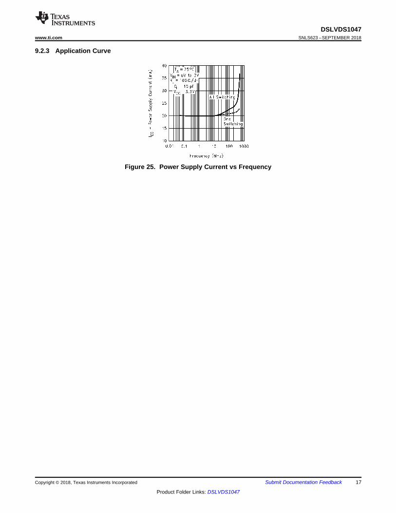
9.2.2.2 Data Rate vs Cable Length Graph Test ProcedureA pseudo-random bit sequence (PRBS) of 29−1 bits was programmed into a function generator (TektronixHFS9009) and connected to the driver inputs through 50-Ω cables and SMB connectors. An oscilloscope(Tektronix 11801B) was used to probe the resulting eye pattern, measured differentially at the input to thereceiver. A 100-Ω resistor was used to terminate the pair at the far end of the cable. The measurements weretaken at the far end of the cable, at the input of the receiver, and used for the jitter analysis for this graph(Figure 17). The frequency of the input signal was increased until the measured jitter (ttcs) equaled 20% withrespect to the unit interval (ttui) for the particular cable length under test. Twenty percent jitter is a reasonableplace to start with many system designs. The data used was NRZ. Jitter was measured at the 0-V differentialvoltage of the differential eye pattern. The DSLVDS1047 and DSLVDS1048 can be evaluated using the newDS90LV047-048AEVM.
Figure 25 shows very good typical performance that can be used as a design guideline for data rate vs cablelength. Increasing the jitter percentage increases the curve respectively, allowing the device to transmit fasterover longer cable lengths. This relaxes the jitter tolerance of the system allowing more jitter into the system,which could reduce the reliability and efficiency of the system. Alternatively, decreasing the jitter percentage hasthe opposite effect on the system. The area under the curve is considered the safe operating area based on theabove signal quality criteria. For more information on eye pattern testing, please see AN-808 Long TransmissionLines and Data Signal Quality (SNLA028).
17
DSLVDS1047www.ti.com SNLS623 –SEPTEMBER 2018
Product Folder Links: DSLVDS1047
Submit Documentation FeedbackCopyright © 2018, Texas Instruments Incorporated
9.2.3 Application Curve
Figure 25. Power Supply Current vs Frequency
18
DSLVDS1047SNLS623 –SEPTEMBER 2018 www.ti.com
Product Folder Links: DSLVDS1047
Submit Documentation Feedback Copyright © 2018, Texas Instruments Incorporated
10 Power Supply RecommendationsAlthough the DSLVDS1047 draws very little power while at rest. At higher switching frequencies there is adynamic current component which increases the overall power consumption. The DSLVDS1047 power supplyconnection must take this additional current consumption into consideration for maximum power requirements.
11 Layout
11.1 Layout Guidelines• Use at least 4 PCB layers (top to bottom); LVDS signals, ground, power, TTL signals.• Isolate TTL signals from LVDS signals, otherwise the TTL may couple onto the LVDS lines. It is best to put
TTL and LVDS signals on different layers which are isolated by a power/ground plane(s).• Keep drivers and receivers as close to the (LVDS port side) connectors as possible.
11.1.1 Power Decoupling RecommendationsBypass capacitors must be used on power pins. Use high frequency ceramic (surface mount is recommended)0.1-µF and 0.001-µF capacitors in parallel at the power supply pin with the smallest value capacitor closest to thedevice supply pin. Additional scattered capacitors over the printed-circuit board improves decoupling. Multiplevias must be used to connect the decoupling capacitors to the power planes. A 10-µF (35-V) or greater solidtantalum capacitor must be connected at the power entry point on the printed-circuit board between the supplyand ground.
11.1.2 Differential TracesUse controlled impedance traces which match the differential impedance of your transmission medium (that is,cable) and termination resistor. Run the differential pair trace lines as close together as possible as soon as theyleave the IC (stubs must be < 10 mm long). This helps eliminate reflections and ensure noise is coupled ascommon-mode. In fact, we have seen that differential signals which are 1 mm apart radiate far less noise thantraces 3 mm apart since magnetic field cancellation is much better with the closer traces. In addition, noiseinduced on the differential lines is much more likely to appear as common-mode which is rejected by thereceiver.
Match electrical lengths between traces to reduce skew. Skew between the signals of a pair means a phasedifference between signals, which destroys the magnetic field cancellation benefits of differential signals andEMI, results.
NOTEThe velocity of propagation, v = c/Er where c (the speed of light) = 0.2997mm/ps or0.0118 in/ps
Do not rely solely on the autoroute function for differential traces. Carefully review dimensions to matchdifferential impedance and provide isolation for the differential lines. Minimize the number or vias and otherdiscontinuities on the line.
Avoid 90° turns (these cause impedance discontinuities). Use arcs or 45° bevels.
Within a pair of traces, the distance between the two traces must be minimized to maintain common-moderejection of the receivers. On the printed-circuit board, this distance must remain constant to avoid discontinuitiesin differential impedance. Minor violations at connection points are allowable.
11.1.3 TerminationUse a termination resistor which best matches the differential impedance or your transmission line. The resistormust be between 90 Ω and 130 Ω. Remember that the current mode outputs need the termination resistor togenerate the differential voltage. LVDS does not work without resistor termination. Typically, connecting a singleresistor across the pair at the receiver end will suffice.
8
7
Decoupling Cap
6
5
4
3
2
1
9
10
11
12
13
14
15
16
VCC
DIN2
DIN1
EN
DIN3
DIN4
EN*
GND
DOUT4-
DOUT4+
DOUT3+
DOUT3-
DOUT2-
DOUT2+
DOUT1+
DOUT1-
DS90LV047A
8
7
6
5
4
3
2
1
9
10
11
12
13
14
15
16
ROUT2
ROUT1
EN
ROUT3
ROUT4
EN*
GND
DS90LV048A
RIN4-
RIN4+
RIN3+
RIN3-
RIN2-
RIN2+
RIN1+
RIN1-
LVCMOS Inputs
VCCDecoupling Cap
Series Termination (optional)
Series Termination (optional)
LVCMOS Outputs
Input Termination (Required)
19
DSLVDS1047www.ti.com SNLS623 –SEPTEMBER 2018
Product Folder Links: DSLVDS1047
Submit Documentation FeedbackCopyright © 2018, Texas Instruments Incorporated
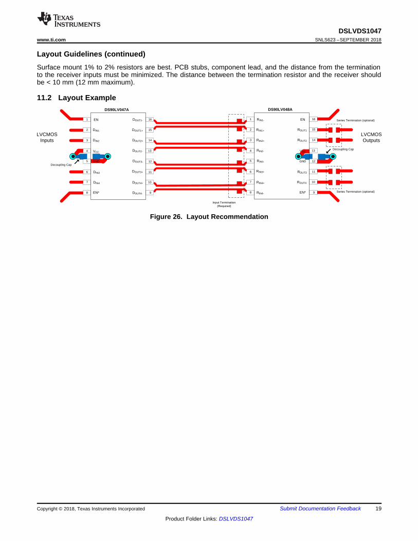
Layout Guidelines (continued)Surface mount 1% to 2% resistors are best. PCB stubs, component lead, and the distance from the terminationto the receiver inputs must be minimized. The distance between the termination resistor and the receiver shouldbe < 10 mm (12 mm maximum).
11.2 Layout Example
Figure 26. Layout Recommendation
20
DSLVDS1047SNLS623 –SEPTEMBER 2018 www.ti.com
Product Folder Links: DSLVDS1047
Submit Documentation Feedback Copyright © 2018, Texas Instruments Incorporated
12 Device and Documentation Support
12.1 Receiving Notification of Documentation UpdatesTo receive notification of documentation updates, navigate to the device product folder on ti.com. In the upperright corner, click on Alert me to register and receive a weekly digest of any product information that haschanged. For change details, review the revision history included in any revised document.
12.2 Community ResourcesThe following links connect to TI community resources. Linked contents are provided "AS IS" by the respectivecontributors. They do not constitute TI specifications and do not necessarily reflect TI's views; see TI's Terms ofUse.
TI E2E™ Online Community TI's Engineer-to-Engineer (E2E) Community. Created to foster collaborationamong engineers. At e2e.ti.com, you can ask questions, share knowledge, explore ideas and helpsolve problems with fellow engineers.
Design Support TI's Design Support Quickly find helpful E2E forums along with design support tools andcontact information for technical support.
12.3 TrademarksE2E is a trademark of Texas Instruments.All other trademarks are the property of their respective owners.
12.4 Electrostatic Discharge CautionThis integrated circuit can be damaged by ESD. Texas Instruments recommends that all integrated circuits be handled withappropriate precautions. Failure to observe proper handling and installation procedures can cause damage.
ESD damage can range from subtle performance degradation to complete device failure. Precision integrated circuits may be moresusceptible to damage because very small parametric changes could cause the device not to meet its published specifications.
12.5 GlossarySLYZ022 — TI Glossary.
This glossary lists and explains terms, acronyms, and definitions.
21
DSLVDS1047www.ti.com SNLS623 –SEPTEMBER 2018
Product Folder Links: DSLVDS1047
Submit Documentation FeedbackCopyright © 2018, Texas Instruments Incorporated
13 Mechanical, Packaging, and Orderable InformationThe following pages include mechanical, packaging, and orderable information. This information is the mostcurrent data available for the designated devices. This data is subject to change without notice and revision ofthis document. For browser-based versions of this data sheet, refer to the left-hand navigation.
PACKAGE OPTION ADDENDUM
www.ti.com 10-Dec-2020
Addendum-Page 1
PACKAGING INFORMATION
Orderable Device Status(1)
Package Type PackageDrawing
Pins PackageQty
Eco Plan(2)
Lead finish/Ball material
(6)
MSL Peak Temp(3)
Op Temp (°C) Device Marking(4/5)
Samples
DSLVDS1047PWR ACTIVE TSSOP PW 16 2500 RoHS & Green SN Level-1-260C-UNLIM -40 to 85 DSLVDS1047
DSLVDS1047PWT ACTIVE TSSOP PW 16 250 RoHS & Green SN Level-1-260C-UNLIM -40 to 85 DSLVDS1047
(1) The marketing status values are defined as follows:ACTIVE: Product device recommended for new designs.LIFEBUY: TI has announced that the device will be discontinued, and a lifetime-buy period is in effect.NRND: Not recommended for new designs. Device is in production to support existing customers, but TI does not recommend using this part in a new design.PREVIEW: Device has been announced but is not in production. Samples may or may not be available.OBSOLETE: TI has discontinued the production of the device.
(2) RoHS: TI defines "RoHS" to mean semiconductor products that are compliant with the current EU RoHS requirements for all 10 RoHS substances, including the requirement that RoHS substancedo not exceed 0.1% by weight in homogeneous materials. Where designed to be soldered at high temperatures, "RoHS" products are suitable for use in specified lead-free processes. TI mayreference these types of products as "Pb-Free".RoHS Exempt: TI defines "RoHS Exempt" to mean products that contain lead but are compliant with EU RoHS pursuant to a specific EU RoHS exemption.Green: TI defines "Green" to mean the content of Chlorine (Cl) and Bromine (Br) based flame retardants meet JS709B low halogen requirements of <=1000ppm threshold. Antimony trioxide basedflame retardants must also meet the <=1000ppm threshold requirement.
(3) MSL, Peak Temp. - The Moisture Sensitivity Level rating according to the JEDEC industry standard classifications, and peak solder temperature.
(4) There may be additional marking, which relates to the logo, the lot trace code information, or the environmental category on the device.
(5) Multiple Device Markings will be inside parentheses. Only one Device Marking contained in parentheses and separated by a "~" will appear on a device. If a line is indented then it is a continuationof the previous line and the two combined represent the entire Device Marking for that device.
(6) Lead finish/Ball material - Orderable Devices may have multiple material finish options. Finish options are separated by a vertical ruled line. Lead finish/Ball material values may wrap to twolines if the finish value exceeds the maximum column width.
Important Information and Disclaimer:The information provided on this page represents TI's knowledge and belief as of the date that it is provided. TI bases its knowledge and belief on informationprovided by third parties, and makes no representation or warranty as to the accuracy of such information. Efforts are underway to better integrate information from third parties. TI has taken andcontinues to take reasonable steps to provide representative and accurate information but may not have conducted destructive testing or chemical analysis on incoming materials and chemicals.TI and TI suppliers consider certain information to be proprietary, and thus CAS numbers and other limited information may not be available for release.
In no event shall TI's liability arising out of such information exceed the total purchase price of the TI part(s) at issue in this document sold by TI to Customer on an annual basis.
PACKAGE OPTION ADDENDUM
www.ti.com 10-Dec-2020
Addendum-Page 2
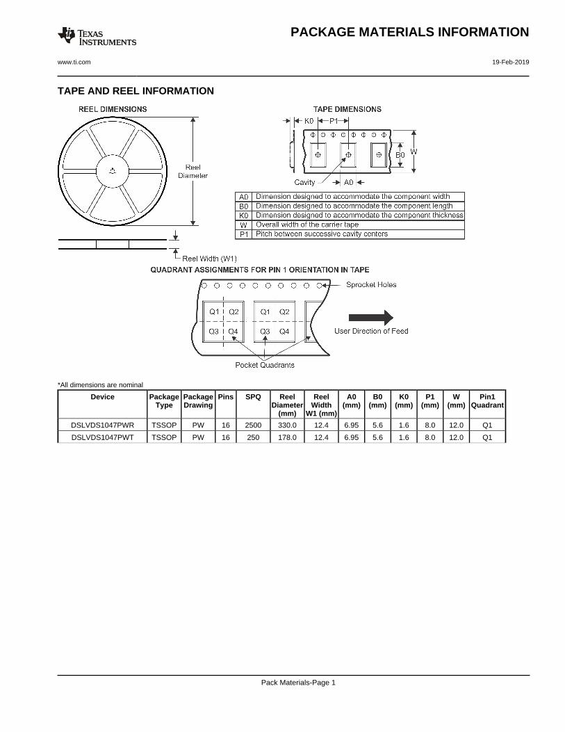
TAPE AND REEL INFORMATION
*All dimensions are nominal
Device PackageType
PackageDrawing
Pins SPQ ReelDiameter
(mm)
ReelWidth
W1 (mm)
A0(mm)
B0(mm)
K0(mm)
P1(mm)
W(mm)
Pin1Quadrant
DSLVDS1047PWR TSSOP PW 16 2500 330.0 12.4 6.95 5.6 1.6 8.0 12.0 Q1
DSLVDS1047PWT TSSOP PW 16 250 178.0 12.4 6.95 5.6 1.6 8.0 12.0 Q1
PACKAGE MATERIALS INFORMATION
www.ti.com 19-Feb-2019
Pack Materials-Page 1
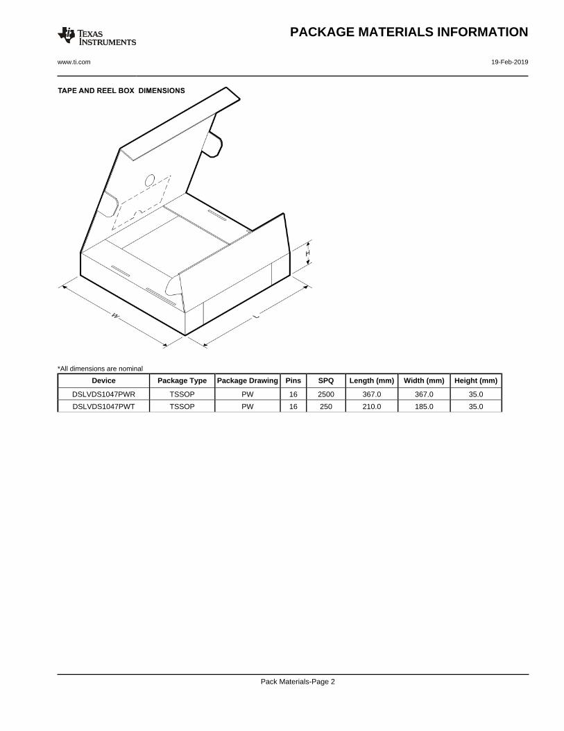
*All dimensions are nominal
Device Package Type Package Drawing Pins SPQ Length (mm) Width (mm) Height (mm)
DSLVDS1047PWR TSSOP PW 16 2500 367.0 367.0 35.0
DSLVDS1047PWT TSSOP PW 16 250 210.0 185.0 35.0
PACKAGE MATERIALS INFORMATION
www.ti.com 19-Feb-2019
Pack Materials-Page 2
www.ti.com
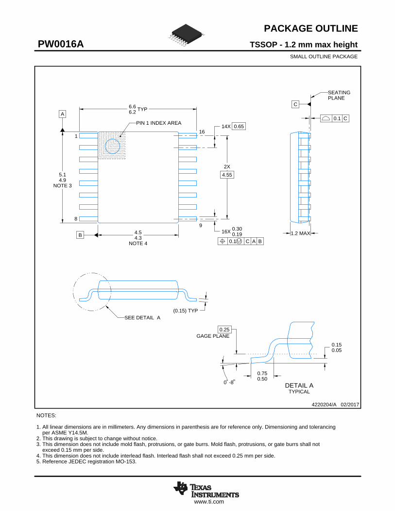
PACKAGE OUTLINE
C
14X 0.65
2X4.55
16X 0.300.19
TYP6.66.2
1.2 MAX
0.150.05
0.25GAGE PLANE
-80
BNOTE 4
4.54.3
A
NOTE 3
5.14.9
0.750.50
(0.15) TYP
TSSOP - 1.2 mm max heightPW0016ASMALL OUTLINE PACKAGE
4220204/A 02/2017
1
89
16
0.1 C A B
PIN 1 INDEX AREA
SEE DETAIL A
0.1 C
NOTES: 1. All linear dimensions are in millimeters. Any dimensions in parenthesis are for reference only. Dimensioning and tolerancing per ASME Y14.5M. 2. This drawing is subject to change without notice. 3. This dimension does not include mold flash, protrusions, or gate burrs. Mold flash, protrusions, or gate burrs shall not exceed 0.15 mm per side. 4. This dimension does not include interlead flash. Interlead flash shall not exceed 0.25 mm per side.5. Reference JEDEC registration MO-153.
SEATINGPLANE
A 20DETAIL ATYPICAL
SCALE 2.500
www.ti.com
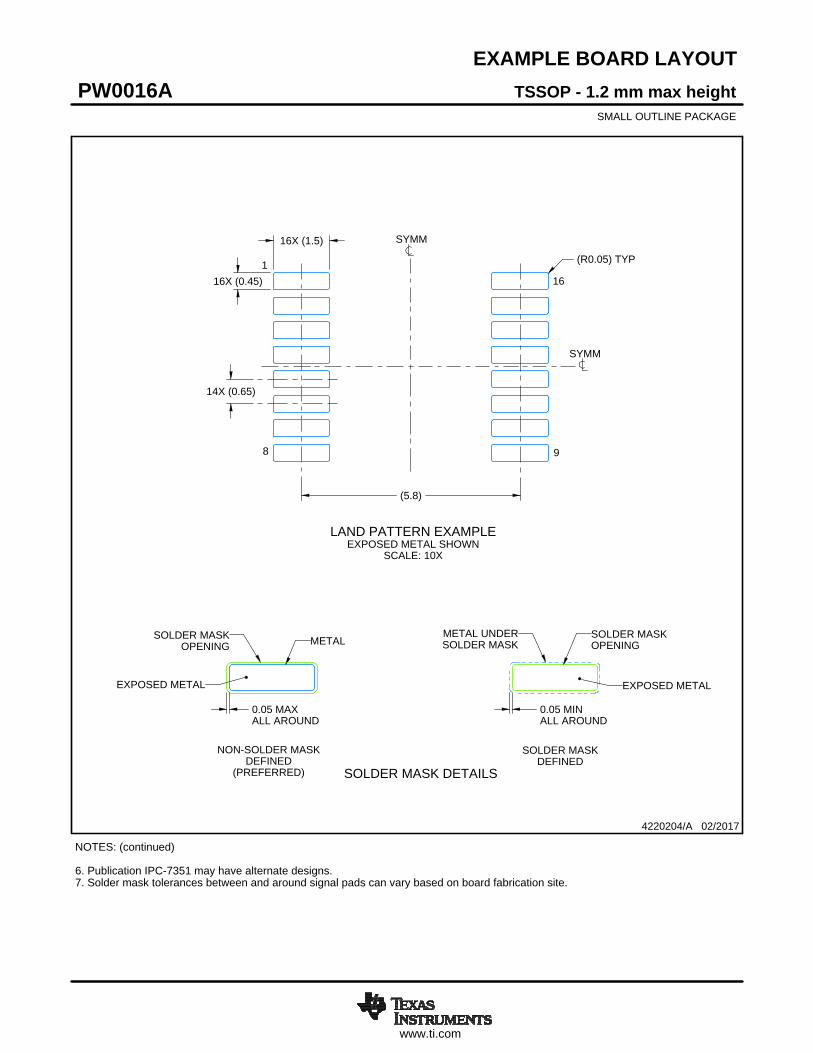
EXAMPLE BOARD LAYOUT
0.05 MAXALL AROUND
0.05 MINALL AROUND
16X (1.5)
16X (0.45)
14X (0.65)
(5.8)
(R0.05) TYP
TSSOP - 1.2 mm max heightPW0016ASMALL OUTLINE PACKAGE
4220204/A 02/2017
NOTES: (continued) 6. Publication IPC-7351 may have alternate designs. 7. Solder mask tolerances between and around signal pads can vary based on board fabrication site.
LAND PATTERN EXAMPLEEXPOSED METAL SHOWN
SCALE: 10X
SYMM
SYMM
1
8 9
16
15.000
METALSOLDER MASKOPENING
METAL UNDERSOLDER MASK
SOLDER MASKOPENING
EXPOSED METALEXPOSED METAL
SOLDER MASK DETAILS
NON-SOLDER MASKDEFINED
(PREFERRED)
SOLDER MASKDEFINED
www.ti.com
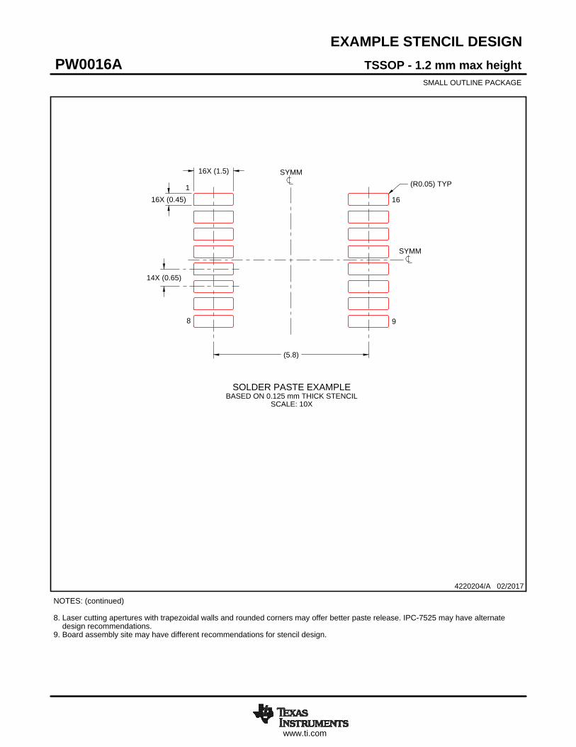
EXAMPLE STENCIL DESIGN
16X (1.5)
16X (0.45)
14X (0.65)
(5.8)
(R0.05) TYP
TSSOP - 1.2 mm max heightPW0016ASMALL OUTLINE PACKAGE
4220204/A 02/2017
NOTES: (continued) 8. Laser cutting apertures with trapezoidal walls and rounded corners may offer better paste release. IPC-7525 may have alternate design recommendations. 9. Board assembly site may have different recommendations for stencil design.
SOLDER PASTE EXAMPLEBASED ON 0.125 mm THICK STENCIL
SCALE: 10X
SYMM
SYMM
1
8 9
16
IMPORTANT NOTICE AND DISCLAIMER
TI PROVIDES TECHNICAL AND RELIABILITY DATA (INCLUDING DATASHEETS), DESIGN RESOURCES (INCLUDING REFERENCE DESIGNS), APPLICATION OR OTHER DESIGN ADVICE, WEB TOOLS, SAFETY INFORMATION, AND OTHER RESOURCES “AS IS” AND WITH ALL FAULTS, AND DISCLAIMS ALL WARRANTIES, EXPRESS AND IMPLIED, INCLUDING WITHOUT LIMITATION ANY IMPLIED WARRANTIES OF MERCHANTABILITY, FITNESS FOR A PARTICULAR PURPOSE OR NON-INFRINGEMENT OF THIRD PARTY INTELLECTUAL PROPERTY RIGHTS.These resources are intended for skilled developers designing with TI products. You are solely responsible for (1) selecting the appropriate TI products for your application, (2) designing, validating and testing your application, and (3) ensuring your application meets applicable standards, and any other safety, security, or other requirements. These resources are subject to change without notice. TI grants you permission to use these resources only for development of an application that uses the TI products described in the resource. Other reproduction and display of these resources is prohibited. No license is granted to any other TI intellectual property right or to any third party intellectual property right. TI disclaims responsibility for, and you will fully indemnify TI and its representatives against, any claims, damages, costs, losses, and liabilities arising out of your use of these resources.TI’s products are provided subject to TI’s Terms of Sale (www.ti.com/legal/termsofsale.html) or other applicable terms available either on ti.com or provided in conjunction with such TI products. TI’s provision of these resources does not expand or otherwise alter TI’s applicable warranties or warranty disclaimers for TI products.
Mailing Address: Texas Instruments, Post Office Box 655303, Dallas, Texas 75265Copyright © 2020, Texas Instruments Incorporated