Embed Size (px)
Citation preview
aPreliminary Technical Data ADSP-TS001
DSPMicrocomputer
This information applies to a product under development. Its characteristics and specifications are subject to change without notice. Analog Devices assumes no obligation regarding future manufacturing unless otherwise agreed to in writing.
One Technology Way http://www.analog.com/dspP.O. Box 9106 Tel: 1-800-ANALOG-DNorwood MA 02062-9106 Fax: 1-781-461-3010U.S.A. Analog Devices Inc., 1998
REV. PrC
KEY FEATURES
• Ultra high-performance 32-bit DSP optimized for computationally demanding, large signal processing tasks and multichannel applications
• Support for IEEE-compatible single-precision float-ing-point and extended-precision floating-point nu-meric formats and 8-, 16-, and 32-bit fixed-point numeric formats
• Static superscalar architecture combines and balances RISC, VLIW, and DSP functionality to provide:
• Load and store architecture that supports 32-, 64-, or 128-bit data through direct or broadcast accesses
• Static branch prediction
• Interlocked, multiport register files; 128 registers
• Instruction-level parallelism determined before runtime
• I/O and internal memory capable of sustaining core rates
• Hardware support for circular buffers, bit reverse, and zero-overhead looping
M 0 A DDR
M 0 DA TA
M 1 A DDR
M 1 DA TA
M 2 A DDR
M 2 DA TA
MEM ORYM 2
64K X 32
A D
MEM ORYM 1
64K X 32
A D
MEM ORYM 0
64K X 32
A D
IN TEGERK A LU
IN TEGERJ ALU
32
DA TA ADDRESS GEN ERA TION
IA B
PC BTB IRQ
A DDRFETCH
PROGRA M SEQ UENCER
YREGISTER
FILE32X32
MULTIPLIER
A LU
SHIFTER
XREGISTER
FILE32X32
MULTIPLIER
A LU
SHIFTER
DAB
128
128
I/O A DDRESS
DA TA
64
IN TERN A L MEM ORY
PROCESSIN G ELEM ENTS I/O PROCESSO R LIN K PORTS
JTAG PORT
SDRA MCON TROLLER
LIN K PORTCON TROLLER
CON TROL/STA TUS/BUFFERS
DM ACO NTRO LLER
CON TROL/STA TUS/
TC B'S
L0
L1
L2
L3
IN PUTFIFO
OUTPUTBUFFER
OUTPUTFIFO
HOSTIN TERFA CE
M ULTI-PROCESSORIN TERFA CE
EXTERN ALPORT
12832 128
DM ADA TA
LIN KDA TA
DM AA DDRESS
4
8
A DDRESS
32
32
128
32
128
32
128
CN TRL
6
32
32
32X32 32X32
4
8
4
8
4
8
CLUSTERBUS
A RBITORDA B
128
128
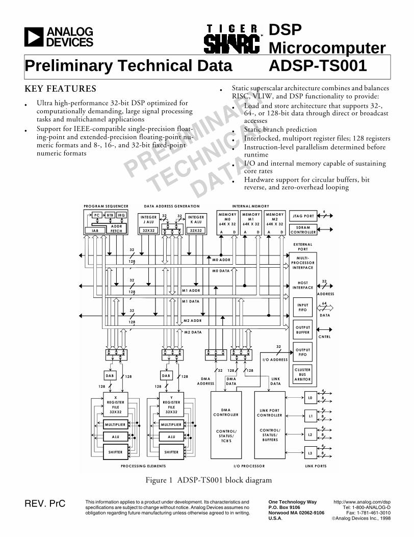
Figure 1 ADSP-TS001 block diagram
December 1999 ADSP-TS001 Preliminary Data SheetFor current information contact Analog Devices at (781) 461-3881
This information applies to a product under development. Its characteristics and specifications are subject to change with-out notice. Analog Devices assumes no obligation regarding future manufacturing unless otherwise agreed to in writing.2 REV. PrC
PERFORMANCE
• Runs at 150 MHz, 6.67ns instruction rate
• Executes from 1 to 4 instructions per cycle; maximum of 6 instructions
• Has internal bandwidth of 7.2 Gbytes/s and performs a complete context switch in <20 cycles (134 ns)
• Executes six single-precision floating-point or twenty-four 16-bit fixed-point operations per cycle (900 MFLOPS or 3.6 GOPS performance)
• Provides 8 MACs/cycle peak and 7.1 MACs/cycle sustained 16-bit performance and 2 MACs/cycle peak and 1.8 MACs/cycle sustained 32-bit performance (based on FIR)
• Executes 8 Add/Compare/Select (ACS) sequences for Viterbi algorithm in < 1 cycle
• Has an 8-cycle instruction pipeline (3-cycle fetch pipe and 5-cycle execution pipe)—computation results available 2 cycles after operation begins
FEATURES
• Fully interruptible programming model with flexible programming in Assembly and C languages
• Single-instruction multiple-data (SIMD) operations supported by two computation blocks, each with an ALU, multiplier, shifter, and 32-word register file
• Integrated peripherals include 6 Mbit on-chip SRAM, glueless multiprocessing features, and ports (link, ex-ternal bus, and JTAG)
• 64-bit generalized bit manipulation unit
• Instruction set
• Algebraic assembly language syntax
• Directly supports all DSP, imaging, and video arithmetic types, eliminating hardware modes
• Branch prediction encoded in instruction, enables zero-overhead loops
• Parallelism encoded in instruction line
• Predicated execution optional for all instructions
• User defines partitioning between program and data memory
• 6 Mbit of on-chip SRAM memory
• Divided into three 2 Mbit banks
• Each bank connects to one of the three128-bit wide internal buses
• Core can access 128 bits from each bank each cycle
• Program stored in quad-words with no wasted space
• Unified, linear memory map for all internal and external memory
• Dual computation blocks
• Each has an ALU, multiplier, 64-bit shifter, and 32-word register file
• Register files are fully orthogonal
• Two-cycle computation pipeline provides results 2 cycles after an operation begins
• Data Alignment Buffer (DAB) enables nonaligned accesses of memory, for efficient implementation of FIR filters
• Each operates on one to eight data elements
• Integer, fractional, signed, and unsigned data types, with optional saturation
• Performs two complex, 16-bit MACs per cycle
• Dual integer ALUs (IALUs)
• Provide memory addresses for data and update pointers
• Support circular buffering and bit-reverse addressing
• Perform general-purpose integer operations, increasing programming flexibility
• Each has a 32-word register file
• 128-entry Branch Target Buffer (BTB) works in conjunction with branch prediction to provide zero-over-head looping

This information applies to a product under development. Its characteristics and specifications are subject to change with-out notice. Analog Devices assumes no obligation regarding future manufacturing unless otherwise agreed to in writing.
ADSP-TS001 Preliminary Data Sheet December 1999For current information contact Analog Devices at (781) 461-3881
3REV. PrC
• Instruction Alignment Buffer (IAB) supports compact code by eliminating the requirement to align code in memory
• Two 32-bit interval timers
• External port
• Connection to 32- or 64-bit wide external bus
• Data transfer rate of 600 Mbytes/s over external bus
• Glueless interface to SDRAM and other off-chip memory and other peripherals
• DMA controller
• Supports fourteen DMA channels
• Performs DMA transfers between internal memory and external memory and memory-mapped periph-erals, the internal memory of other DSPs on a common bus, a host processor, or link port I/O; between external memory and external peripherals or link port I/O; and between an external bus master and in-ternal memory or link port I/O
• Multiprocessor interface supports up to eight DSPs on a common bus
• On-chip arbitration for glueless multiprocessing
• Globally accessible internal registers and memory
• Semaphore support
• Four link ports
• Hardware-controlled, full-duplex (one transmit and one receive port per link)
• DMA data transfer rate of 150 Mbytes/s (double data rate)
• Four general-purpose flag I/O ports
• Standard 1149.1 IEEE JTAG test access port and on-chip emulation
• Debug functionality available through a debug monitor or the JTAG test access port
• Three sets of programmable memory-address watch points, able to operate in parallel, enable users to design a set of conditions at which to halt and examine the state of the DSP
• Eight trace buffers enable users to recreate the path taken by the program for the last four to eight branches
• Performance monitors indicate the number of times a specified event occurs during a run
• User and Supervisor modes available for OS kernel and debug monitor support
GENERAL DESCRIPTION
The ADSP-TS001 TigerSHARC 32-bit DSP is a high-performance, static superscalar, next generation SHARC processor. It combines dual computation blocks with native support for 32- and 40-bit floating-point and 8-, 16-, 32-, and 64-bit fixed-point processing with very wide memory widths to set a new standard of performance for digital signal processors. Its static superscalar architecture enables the DSP each cycle to execute up to six instructions, performing twenty-four 16-bit fixed-point operations or six floating-point operations.
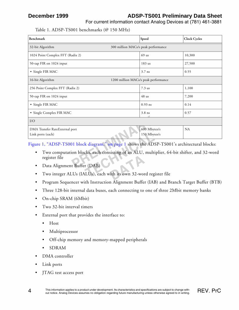
Three independent 128-bit wide internal data buses, each connecting to one of the three 2 Mbit memory banks, enable quad-word data, instruction, and I/O accesses and provide 7.2 Gbytes/sec of internal memory bandwidth. Operating at 150 MHz, the ADSP-TS001’s core has a 6.67ns instruction cycle time. Using its SIMD features, the ADSP-TS001 can perform 1200 million 40-bit MACs or 300 million 80-bit MACs per second. Table 1 shows the DSP’s performance benchmarks.
December 1999 ADSP-TS001 Preliminary Data SheetFor current information contact Analog Devices at (781) 461-3881
This information applies to a product under development. Its characteristics and specifications are subject to change with-out notice. Analog Devices assumes no obligation regarding future manufacturing unless otherwise agreed to in writing.4 REV. PrC
Figure 1, “ADSP-TS001 block diagram,” on page 1 shows the ADSP-TS001’s architectural blocks:
• Two computation blocks, each consisting of an ALU, multiplier, 64-bit shifter, and 32-word register file
• Data Alignment Buffer (DAB)
• Two integer ALUs (IALUs), each with its own 32-word register file
• Program Sequencer with Instruction Alignment Buffer (IAB) and Branch Target Buffer (BTB)
• Three 128-bit internal data buses, each connecting to one of three 2Mbit memory banks
• On-chip SRAM (6Mbit)
• Two 32-bit interval timers
• External port that provides the interface to:
• Host
• Multiprocessor
• Off-chip memory and memory-mapped peripherals
• SDRAM
• DMA controller
• Link ports
• JTAG test access port
Table 1. ADSP-TS001 benchmarks (@ 150 MHz)
Benchmark Speed Clock Cycles
32-bit Algorithm 300 million MACs/s peak performance
1024 Point Complex FFT (Radix 2) 69 us 10,300
50-tap FIR on 1024 input 183 us 27,500
• Single FIR MAC 3.7 ns 0.55
16-bit Algorithm 1200 million MACs/s peak performance
256 Point Complex FFT (Radix 2) 7.3 us 1,100
50-tap FIR on 1024 input 48 us 7,200
• Single FIR MAC 0.93 ns 0.14
• Single Complex FIR MAC 3.8 ns 0.57
I/O
DMA Transfer RateExternal port
Link ports (each)
600 Mbytes/s
150 Mbytes/s
NA
This information applies to a product under development. Its characteristics and specifications are subject to change with-out notice. Analog Devices assumes no obligation regarding future manufacturing unless otherwise agreed to in writing.
ADSP-TS001 Preliminary Data Sheet December 1999For current information contact Analog Devices at (781) 461-3881
5REV. PrC
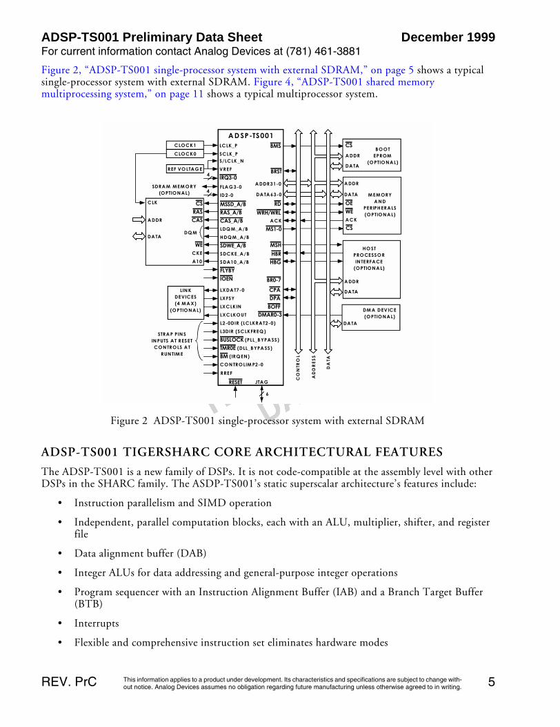
Figure 2, “ADSP-TS001 single-processor system with external SDRAM,” on page 5 shows a typical single-processor system with external SDRAM. Figure 4, “ADSP-TS001 shared memory multiprocessing system,” on page 11 shows a typical multiprocessor system.
ADSP-TS001 TIGERSHARC CORE ARCHITECTURAL FEATURES
The ADSP-TS001 is a new family of DSPs. It is not code-compatible at the assembly level with other DSPs in the SHARC family. The ASDP-TS001’s static superscalar architecture’s features include:
• Instruction parallelism and SIMD operation
• Independent, parallel computation blocks, each with an ALU, multiplier, shifter, and register file
• Data alignment buffer (DAB)
• Integer ALUs for data addressing and general-purpose integer operations
• Program sequencer with an Instruction Alignment Buffer (IAB) and a Branch Target Buffer (BTB)
• Interrupts
• Flexible and comprehensive instruction set eliminates hardware modes
DM A DEVICE(OPTIONA L)
DA TA
DMAR0-3
4
RESET JTAG
6
A D SP-TS001BMSCLOCK1
LIN KDEVICES(4 M A X)
(OPTIONA L)LXCLKIN
L2-0DIR (LCLKRAT2-0)
LXDA T7-0
LXCLKOUT
LXFSY
L3DIR (SCLKFREQ)
CSBOOT
EPROM(OPTIONA L)
A DDR
M EM ORYA ND
PERIPHERALS(OPTIONA L)
OE
DA TA
A DDR
DA TA
HO STPROCESSORIN TERFACE
(OPTIONA L)
A CK
BR0-7
IRQ3-04
FLA G3-0
TMR0E (DLL_BYPA SS)
ID2-0
CPA
HBGHBR
MS1-0
DA TA 63-0
DA TA
A DDR
CS
A CK
WE
A DDR31-0
DA
TA
CO
NTR
OL
AD
DR
ES
S
BRST
LCLK_P
S/LCLK_N
RD
WRH/WRL
MSH
MSSD_A/B
FLYBYIOEN
RAS_A/BCAS_A/BLDQ M_A /B
HDQM_A/B
SDWE_A/BSDCKE_A/B
SDA10_A /B
DPA
BOFF
BUSLOCK (PLL_BYPA SS)
BM (IRQEN)
CON TROLIM P2-0
VREF
RREF
REF VO LTAG E
STRA P PIN SIN PUTS A T RESETCON TROLS A T
RUN TIM E
SDRA M MEM ORY(OPTION AL)
CSRASCAS
DQ M
WECKE
A10
A DDR
DA TA
CLK
CLOCK0 SCLK_P
Figure 2 ADSP-TS001 single-processor system with external SDRAM

December 1999 ADSP-TS001 Preliminary Data SheetFor current information contact Analog Devices at (781) 461-3881
This information applies to a product under development. Its characteristics and specifications are subject to change with-out notice. Analog Devices assumes no obligation regarding future manufacturing unless otherwise agreed to in writing.6 REV. PrC
Instruction Parallelism and SIMD Operation
As a static superscalar DSP, the ADSP-TS001’s core can execute simultaneously from one to four 32-bit instructions encoded in an instruction line. With few exceptions, an instruction line, whether it contains one, two, three, or four 32-bit instructions, executes with a throughput of one cycle in an eight-deep processor pipeline.
The DSP has a set of instruction parallelism rules that programmers must follow when encoding an instruction line. In general, the selection of instructions the DSP can execute in parallel each cycle depends on the instruction line resources each requires and on the source and destination registers used. The programmer has direct control of three core components—the IALUs, the Computation Blocks, and the Program Sequencer.
The ADSP-TS001, in most cases, has a two-cycle execution pipeline that is fully interlocked, so whenever a computation result is unavailable for another operation dependent on it, the DSP automatically inserts stall cycles. Efficient programming with dependency-free instructions can eliminate most computational and memory transfer data dependencies.
Instruction parallelism rules and data dependencies are documented in detail in the DSP’s user’s guide.
In addition, the ADSP-TS001 supports SIMD operations two ways—SIMD Compute Blocks and SIMD computations.The programmer can direct both Compute Blocks to operate on the same data (broadcast distribution) or on different data (merged distribution). In addition, each Compute Block can execute four 16-bit or eight 8-bit SIMD computations in parallel.
Independent, Parallel Compute Blocks
The ADSP-TS001 has two computation blocks, called Compute Blocks, that can operate either independently in parallel or as a Single Instruction Multiple Data (SIMD) engine. The DSP can issue up to two compute instructions per Compute Block each cycle, instructing the ALU, multiplier, or shifter to perform independent, simultaneous operations.
The Compute Blocks are referenced as CBX and CBY, and each contains three computational units—an ALU, a multiplier, a 64-bit shifter—and a 32-word register file.
• Register File—Each Compute Block has a multiported 32-word register file used for transfer-ring data between the computation units and data buses and for storing intermediate results. Instructions can access the registers in the register file individually (word-aligned), or in sets of two (dual-aligned) or four (quad-aligned).
• ALU—The ALU performs a standard set of arithmetic operations in both fixed- and float-ing-point formats. It also performs logic operations.
• Multiplier—The multiplier performs both fixed- and floating-point multiplication and fixed-point multiply and accumulate.
• Shifter—The 64-bit shifter performs logical and arithmetic shifts, bit and bitstream manipula-tion, and field deposit and extraction operations.
Data Alignment Buffer (DAB)
The DAB is a two quad-word FIFO that enables loading of quad-word data from nonaligned addresses.
This information applies to a product under development. Its characteristics and specifications are subject to change with-out notice. Analog Devices assumes no obligation regarding future manufacturing unless otherwise agreed to in writing.
ADSP-TS001 Preliminary Data Sheet December 1999For current information contact Analog Devices at (781) 461-3881
7REV. PrC
Normally, load instructions must be aligned to their data size so that quad words are loaded from a quad-aligned address. Using the DAB significantly improves the efficiency of some applications, such as FIR filters.
IALUs
The ADSP-TS001 has two integer ALUs (IALUs) that provide powerful address generation capabilities and perform many general-purpose integer operations. Each IALU has a multiported 32-word register file.
As address generators, the IALUs perform immediate or indirect (pre- and postmodify) addressing. They perform modulus and bit-reverse operations with no constraints placed on memory addresses for data buffer placement. Each IALU can specify either a single-, dual- or quad-word access from memory.
The IALUs enable implementation of circular data buffers in hardware. Circular buffers facilitate efficient programming of delay lines and other data structures required in digital signal processing, and they are commonly used in digital filters and Fourier transforms. Each IALU provides registers for four circular buffers, so applications can set up a total of eight circular buffers. The IALUs handle address pointer wraparound automatically, reducing overhead, increasing performance, and simplifying implementation. Circular buffers can start and end at any memory location.
Because the IALU’s computational pipeline is one cycle deep, integer results are available in the next cycle. Hardware (register dependency check) causes a stall if a result is unavailable in a given cycle.
Program Sequencer
To manage program structures and program flow, the program sequencer:
• Supplies addresses to memory for instruction fetches.
The instruction alignment buffer (IAB) caches up to five fetched instruction lines waiting to execute. The Program Sequencer extracts an instruction line from the IAB and distributes it to the appropriate core component for execution.
• Determines program flow according to JUMP, CALL, RTI, RTS instructions, loop structures, conditions, interrupts, and software exceptions.
• Using branch prediction and a 128-entry branch target buffer (BTB), reduces branch delays for efficient execution of conditional and unconditional branch instructions.
Correctly predicted branches that are taken occur with zero overhead cycles, overcoming the 2- to 6-stage branch penalty.
• Decrements the loop counters.
• Handles hardware interrupts with high throughput and no aborted instruction cycles.
Interrupts
The DSP supports nested and nonnested interrupts. Each interrupt has a register in the interrupt vector table, the interrupt latch register, and the interrupt mask register. All interrupts are fixed as either level-sensitive or edge-sensitive, except the IRQ3-0 hardware interrupts, which are programmable.
The DSP distinguishes between hardware interrupts and software exceptions, handling them differently. When a software exception occurs, the DSP aborts all other instructions in the instruction
December 1999 ADSP-TS001 Preliminary Data SheetFor current information contact Analog Devices at (781) 461-3881
This information applies to a product under development. Its characteristics and specifications are subject to change with-out notice. Analog Devices assumes no obligation regarding future manufacturing unless otherwise agreed to in writing.8 REV. PrC
pipe. When a hardware interrupt occurs, the DSP continues to execute instructions already in the instruction pipe.
Flexible Instruction Set
The 128-bit instruction line, which can contain up to four 32-bit instructions, accommodates a variety of parallel operations for concise programming. For example, one instruction line can direct the DSP to conditionally execute a multiply, an add, and a subtract in both computation blocks while it also branches to another location in the program.
The instruction set directly supports all DSP, image, and video arithmetic types, including signed, unsigned, fractional, and integer data types. This frees the DSP from hardware modes and associated wasted cycles and simplifies compiler operation.
ADSP-TS001 MEMORY AND I/O INTERFACE FEATURES
The ASDP-TS001 includes these memory and I/O interface components and features:
• On-chip SRAM Memory
• Off-chip memory and peripherals interfaces through the external port
• Host interface
• Multiprocessing interface
• SDRAM interface
• EPROM interface
• DMA controller
• Link ports
On-Chip SRAM Memory
The ADSP-TS001 has 6Mbits of on-chip SRAM memory, divided into three blocks of 2Mbits (64K words × 32bits). Each block—M0, M1, and M2—can store program, data, or both, so applications can configure memory to suit their specific needs. However, placing program instructions and data in different memory blocks enables the DSP to access data while it performs an instruction fetch.
Each memory block connects to one of the 128-bit wide internal buses—block M0 to bus MD0, block M1 to bus MD1, and block M2 to bus MD2—enabling the DSP to perform three memory transfers in the same cycle. The DSP’s internal bus architecture provides a total memory bandwidth of 7.2 Gbytes/second, enabling the core and I/O to access eight 32-bit data words (256 bits) and four 32-bit instructions each cycle.
The DSP’s flexible memory structure enables:
• The DSP’s core and I/O to access different memory blocks in the same cycle.
• The DSP’s core to access all three memory blocks in parallel (one instruction and two data ac-cesses)
• Applications to define the partition between program and data memory.
• Applications to access all memory as 32-, 64, or 128-bit words (and 16-bit words with DAB).
This information applies to a product under development. Its characteristics and specifications are subject to change with-out notice. Analog Devices assumes no obligation regarding future manufacturing unless otherwise agreed to in writing.
ADSP-TS001 Preliminary Data Sheet December 1999For current information contact Analog Devices at (781) 461-3881
9REV. PrC
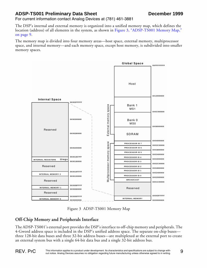
The DSP’s internal and external memory is organized into a unified memory map, which defines the location (address) of all elements in the system, as shown in Figure 3, “ADSP-TS001 Memory Map,” on page 9.
The memory map is divided into four memory areas—host space, external memory, multiprocessor space, and internal memory—and each memory space, except host memory, is subdivided into smaller memory spaces.
Off-Chip Memory and Peripherals Interface
The ADSP-TS001’s external port provides the DSP’s interface to off-chip memory and peripherals. The 4-Gword address space is included in the DSP’s unified address space. The separate on-chip buses—three 128-bit data buses and three 32-bit address buses—are multiplexed at the external port to create an external system bus with a single 64-bit data bus and a single 32-bit address bus.
INTE RN AL RE GIS TE RS
INTE RNAL M E M O RY 2
INTE RNAL M E M O RY 1
INTE RNAL ME M O RY 0
0X 003FFFFF
0X 00300000
0X 00280000
0X 00200000
0X 001807FF
0X 00180000
0X 0010FF FF
0X 00100000
0X 0008FF FF
0X 00080000
0X 0000FF FF
0X 00000000
Interna l Space
Ureg s
Reserved
Reserved
Reserved
Reserved
PROCE SS O R ID 7
PROCE SS O R ID 6
PROCE SS O R ID 5
PROCE SS O R ID 4
PROCE SS O R ID 3
PROCE SS O R ID 2
PROCE SS O R ID 1
PROCE SS O R ID 0
BRO ADC AS T
Host
Bank 1
Bank 0
SDRAM
INTE RNAL M E M ORY
0X 10000000
0X 0C000000
0X 08000000
0X 04000000
0X 03C00000
0X 03800000
0X 03400000
0X 03000000
0X 02C00000
0X 02800000
0X 02400000
0X 02000000
0X 01C00000
0X 003F FFFF
0X 00000000
G lobal Space0X FFF FFFFF
Reserved
Mu
ltip
roce
sso
r m
em
ory
sp
ac
eE
xte
rna
l me
mo
ry s
pa
ceMS1
MS0
Figure 3 ADSP-TS001 Memory Map

December 1999 ADSP-TS001 Preliminary Data SheetFor current information contact Analog Devices at (781) 461-3881
This information applies to a product under development. Its characteristics and specifications are subject to change with-out notice. Analog Devices assumes no obligation regarding future manufacturing unless otherwise agreed to in writing.10 REV. PrC
When the system bus is configured for 64-bit operation, the lower 32 bits of the external data bus connect to even addresses, and the upper 32 bits connect to odd addresses.
The external port supports pipelined, slow, and SDRAM protocols. Addressing of external memory devices and memory-mapped peripherals is facilitated by on-chip decoding of high-order address lines to generate memory bank select signals.
The ADSP-TS001 provides programmable memory, pipeline depth, and idle cycle for synchronous accesses, and external acknowledge controls to support interfacing to pipelined or slow devices, host processors, and other memory-mapped peripherals with variable access, hold, and disable time requirements.
Host Interface
The ADSP-TS001 provides an easy and configurable interface between its external bus and host processors. To accommodate a variety of host processors, the host interface supports pipelined or slow protocols for accesses of the host as slave. Each protocol has programmable transmission parameters, such as idle cycles, pipe depth, and internal wait cycles.
The host interface supports burst transactions initiated by a host processor. After the host issues the starting address of the burst and asserts the BRST signal, the DSP increments the address internally while the host continues to assert BRST.
The host interface provides a deadlock recovery mechanism that enables a host to recover from deadlock situations involving the DSP. The BOFF signal provides the deadlock recovery mechanism. When the host asserts BOFF, the DSP asserts HBG and relinquishes the external bus, even when buslock is enabled.
The host can directly read or write the internal memory of the ADSP-TS001, and it can access most of the DSP registers, including DMA control and TCB registers. Vector interrupts support efficient execution of host commands.
Multiprocessor Interface
The ADSP-TS001 offers powerful features tailored to multiprocessing DSP systems. The external port and link ports provide integrated, glueless multiprocessing support.
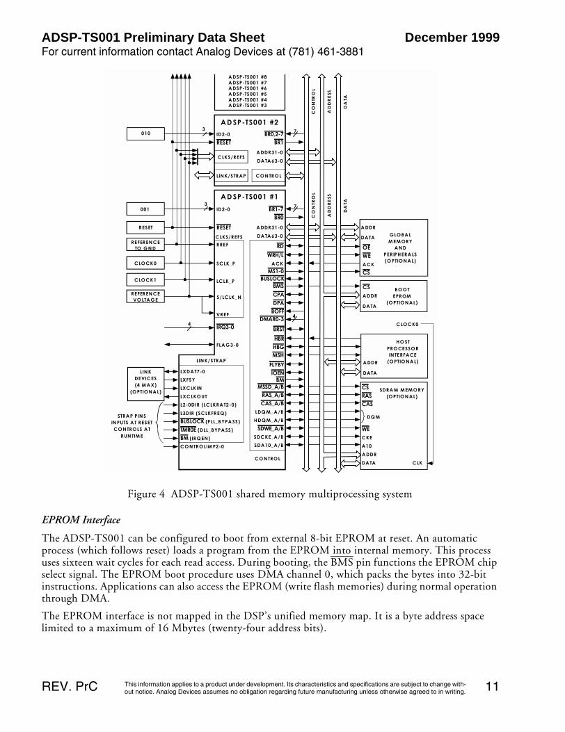
The external port supports a unified address space (see Figure 4, “ADSP-TS001 shared memory multiprocessing system,” on page 11) that enables direct interprocessor accesses of each ADSP-TS001’s internal memory and registers. The DSP’s on-chip distributed bus arbitration logic provides simple, glueless connection for systems containing up to eight ADSP-TS001s and a host processor. Bus arbitration has a rotating priority. Bus lock supports indivisible read-modify-write sequences for semaphores. A bus fairness feature prevents one DSP from holding the external bus too long.
Maximum throughput for interprocessor data transfers is 600 Mbytes/second over the external port.
The DSP’s four link ports provide a second path for interprocessor communications.
SDRAM Interface
The SDRAM interface enables the ADSP-TS001 to transfer data to and from synchronous DRAM (SDRAM) at a throughput of one word per SCLK cycle.
The SDRAM interface provides a glueless interface with standard SDRAMs—16Mb, 64Mb, 128Mb, and 256Mb. The DSP supports directly a maximum of 64Mwords × 32b of SDRAM. The SDRAM interface is mapped in external memory in the DSP’s unified memory map.
This information applies to a product under development. Its characteristics and specifications are subject to change with-out notice. Analog Devices assumes no obligation regarding future manufacturing unless otherwise agreed to in writing.
ADSP-TS001 Preliminary Data Sheet December 1999For current information contact Analog Devices at (781) 461-3881
11REV. PrC
EPROM Interface
The ADSP-TS001 can be configured to boot from external 8-bit EPROM at reset. An automatic process (which follows reset) loads a program from the EPROM into internal memory. This process uses sixteen wait cycles for each read access. During booting, the BMS pin functions the EPROM chip select signal. The EPROM boot procedure uses DMA channel 0, which packs the bytes into 32-bit instructions. Applications can also access the EPROM (write flash memories) during normal operation through DMA.
The EPROM interface is not mapped in the DSP’s unified memory map. It is a byte address space limited to a maximum of 16 Mbytes (twenty-four address bits).
CLKS/REFS
A DDR31-0
DA TA 63-0
7
BR1BR0,2-7
A DDR31-0
DA TA 63-0
7
BR0BR1-7
BMS
CON TROL
A D SP-TS001 #1
CON TROL
A D SP-TS001 #2
A DSP-TS001 #8A DSP-TS001 #7A DSP-TS001 #6A DSP-TS001 #5A DSP-TS001 #4A DSP-TS001 #3
RESET RESET
RREF
ID2-03
001
CLOCK0
LCLK_P
S/LCLK_N
VREF
SCLK_P
CLOCK1
REFEREN CEVO LTA GE
A DDR
DA TA
HO STPROCESSORIN TERFACE
(OPTIONA L)
A CK
GLOBA LM EM ORY
A NDPERIPHERA LS(OPTIONA L)
OE
A DDR
DA TA
CS
A DDR
DA TA
BOOTEPROM
(OPTIONA L)
RD
MS1-0A CK
ID2-03
010
HBGHBR
CS
WEWRH/L
CO
NTR
OL
AD
DR
ESS
DA
TA
CO
NTR
OL
AD
DR
ESS
DA
TA
SDRA M MEM ORY(OPTION AL)
MSSD_A/B
FLYBYIOEN
RAS_A/BCAS_A/B
LDQ M_A/B
HDQM_A/B
SDWE_A/BSDCKE_A/B
SDA10_A/B
CSRASCAS
DQ M
WECKE
A10
A DDR
DA TA CLK
MSH
DMAR0-3
DPABOFF
CPA
BRST
4
LIN KDEVICES(4 M A X)
(OPTIONA L)LXCLKIN
L2-0DIR (LCLKRA T2-0)
LXDA T7-0
LXCLKOUT
LXFSY
L3DIR (SCLKFREQ)
TMR0E (DLL_BYPA SS)
BUSLOCK (PLL_BYPA SS)
BM (IRQEN)
CON TROLIM P2-0
STRA P PIN SIN PUTS A T RESETCON TROLS A T
RUN TIM E
LIN K/STRAP
IRQ3-04
FLA G3-0
LIN K/STRAP
CLKS/REFS
RESET
REFEREN CETO GN D
BUSLOCK
BM
CLOCK0
Figure 4 ADSP-TS001 shared memory multiprocessing system

December 1999 ADSP-TS001 Preliminary Data SheetFor current information contact Analog Devices at (781) 461-3881
This information applies to a product under development. Its characteristics and specifications are subject to change with-out notice. Analog Devices assumes no obligation regarding future manufacturing unless otherwise agreed to in writing.12 REV. PrC
DMA Controller
The ADSP-TS001’s on-chip DMA controller, with fourteen DMA channels, provides zero-overhead data transfers without processor intervention. The DMA controller operates independently and invisibly to the DSP’s core, enabling DMA operations to occur while the DSP’s core continues to execute program instructions.
The DMA controller performs the following DMA operations:
• External port block transfers
Four dedicated bidirectional DMA channels transfer blocks of data between the DSP’s internal memory and any memory-mapped peripheral on the external bus. These transfers support mas-ter mode and handshake mode protocols.
• Link port transfers
Eight dedicated DMA channels (four transmit and four receive) transfer quad-word data only between link ports and between a link port and internal or external memory. These transfers use handshake mode protocol only. DMA priority rotates between the four receive channels.
• AutoDMA transfers
Two dedicated unidirectional DMA channels transfer data received from an external bus master to internal memory or to link port I/O. These transfers use slave mode protocol only, and an external bus master must initiate the transfer.
The DMA controller provides these additional features:
• Flyby transfers
Flyby operations occur through the external port only (DMA channel 0) and do not involve the DSP’s core. The DMA controller acts as a conduit to transfer data from one external device to another through external memory. During a transaction, the DSP relinquishes the external data bus and outputs addresses, memory selects (MS1-0), FLYBY, RD/WR strobes, and responds to ACK.
• DMA chaining
DMA chaining operations enable applications to automatically link one DMA transfer sequence to another for continuous transmission. The sequences can occur over different DMA channels and have different transmission attributes.
• Two-dimensional transfers
The DMA controller can access and transfer 2-D memory arrays on any DMA transmit or re-ceive channel. These transfers are implemented with index, count, and modify registers for both the X and Y dimensions.
Link Ports
The DSP’s four link ports provide additional eight-bit bidirectional I/O capability. With the ability to operate at a double data rate—latching data on both the rising and falling edges of the clock—running at 75 MHz, each link port can support up to 150 Mbytes/second, for a combined maximum throughput of 600 Mbytes/second.

This information applies to a product under development. Its characteristics and specifications are subject to change with-out notice. Analog Devices assumes no obligation regarding future manufacturing unless otherwise agreed to in writing.
ADSP-TS001 Preliminary Data Sheet December 1999For current information contact Analog Devices at (781) 461-3881
13REV. PrC
The link ports provide an optional communications channel that is useful in multiprocessor systems for implementing point-to-point interprocessor communications. Applications can also use the link ports for booting.
Each link port has its own double-buffered input and output registers. The DSP’s core can write directly to a link port’s transmit register and read from a receive register, or the DMA controller can perform DMA transfers through eight (four transmit and four receive) dedicated link port DMA channels.
Each link port has five signals that control its operation: LxCLKOUT and LxCLKIN implement clock/acknowledge handshaking. LxDIR indicates the direction of transfer and is used only when buffering the LxDAT signals; for example, using differential low-swing buffers for long twisted-pair wires. LxDAT provide the data bus 8-bit input/output. LxFSY provides frame synchronization to signal the completion of a block transfer.
The LxFSY signal supports Time Division Multiplex (TDM) applications. Frame synchronization enables applications to connect the link ports to devices that may not transmit bytes in multiples of quad-words, and to handle transfers in which the length of the data is unknown before transmission.
Applications can program separate error detection mechanisms for transmit and receive operations (applications can use the checksum mechanism to implement consecutive link port transfers), the size of data packets, and the speed at which bytes are transmitted.
Under certain conditions, the link port transmitter can initiate a token switch to reverse the direction of transfer; the transmitter then becomes the receiver and vice versa.
ADDITIONAL OPERATIONAL FEATURES
Timer and General-Purpose I/O
The ADSP-TS001 has a timer pin (TMROE) that generates output when a programmed timer counter has expired and four programmable general-purpose I/O pins (FLAG3-0) that can function as either single-bit input or output. As outputs, these pins can signal peripheral devices; as inputs, they can provide the test for conditional branching.
Reset and Booting
The ADSP-TS001 has three levels of reset:
• Power-up reset—After power-up of the system and strap options are stable, the RESET pin must be asserted for at least 1 ms. after the power supply is stable.
• Normal reset—If the power and strap options were set more than 1 ms. before the reset, the RESET pin must be asserted for at least 100 SCLK cycles.
• Core reset—When setting the SQRST bit in SQCTL, the core is reset, but not the external port or I/O.
After reset, the ADSP-TS001 has four boot options for beginning operation:
• Boot from EPROM
The DSP defaults to EPROM booting when the BMS pin is used as the strap option. When the BMS pin is not connected to VCC, the mode is boot from EPROM.
• Boot by an external master (host or another ADSP-TS001)
December 1999 ADSP-TS001 Preliminary Data SheetFor current information contact Analog Devices at (781) 461-3881
This information applies to a product under development. Its characteristics and specifications are subject to change with-out notice. Analog Devices assumes no obligation regarding future manufacturing unless otherwise agreed to in writing.14 REV. PrC
Any master on the cluster bus can boot the ADSP-TS001 through various writes to its internal memory and registers.
• Boot by link port
All four receive link DMA channels are initialized after reset to transfer a 256-word block to internal memory address 0 to 255, and to issue an interrupt at the end of the block (similar to EP DMA). The corresponding DMA interrupts are set to address zero (0).
• No boot—Start running from an external memory
Using the ‘no boot’ option, the ADSP-TS001 must start running from an external memory, caused by asserting one of the IRQ interrupt signals.
The ADSP-TS001 core always exits to reset in the idle state and waits for an interrupt. Some of the interrupts in the IVT are initialized and enabled after reset.
Low-Power Operation
The ADSP-TS001 can enter a low-power sleep mode, in which its core does not execute instructions, reducing power consumption to a minimum. The ADSP-TS001 exits sleep mode when it senses a falling edge on any of its IRQ0-3 interrupt inputs. The interrupt, if enabled, causes the ADSP-TS001 to execute the corresponding interrupt service routine.
This feature is useful for systems that require a low-power standby mode.
Clock Domains
The ADSP-TS001 has two clock inputs that drive its two major clock domains:
• SCLK (system clock)
Provides clock input for the external bus interface and defines the AC specification. The external bus interface runs at 1x the SCLK frequency. A PLL phase locks internal SCLK to SCLK input. The maximum SCLK frequency is ≤½ the internal DSP clock (CCLK) frequency.
• LCLK (local clock)
Provides clock input to the internal clock driver, CCLK, which is internal clock for the core, internal buses, memory, and link ports. The instruction execution rate is equal to CCLK. A PLL from LCLK generates CCLK which is phase-locked. The LCLKRAT pins define the clock mul-tiplication of LCLK to CCLK (see page 26). The link port clock is generated from CCLK via a software programmable divisor.
Connecting SCLK and LCLK to the same clock source and using an integer clock multiplication value provides predictable cycle-by-cycle operation, a requirement of fault-tolerant systems and some multiprocessing systems.
Power Supplies
The ADSP-TS001 has separate power supply connections for internal logic (VDD), analog circuits (VDD_A), reference resistor control (VDD_E), and I/O buffer (VDD_IO) power supplies. The internal (VDD) and analog (VDD_A) supplies must meet the 2.5V requirement. The reference resistor control (VDD_E) and I/O buffer (VDD_IO) supplies must meet the 3.3V requirement.
Note that the analog (VDD_A) supply powers the clock generator PLL, and the reference resistor control (VDD_E) powers the controlled impedance circuit. To produce a stable clock, you must provide an
This information applies to a product under development. Its characteristics and specifications are subject to change with-out notice. Analog Devices assumes no obligation regarding future manufacturing unless otherwise agreed to in writing.
ADSP-TS001 Preliminary Data Sheet December 1999For current information contact Analog Devices at (781) 461-3881
15REV. PrC
external circuit to filter the power inputs to VDD_A and VDD_E as shown in Figure 5 below and Figure 6 on page 16.
The ideal power on sequence for the DSP is to provide power up of all supplies simultaneously. If there is going to be some delay between power up of the supplies, provide VDD_IO first, then VDD.
Filtering Circuits
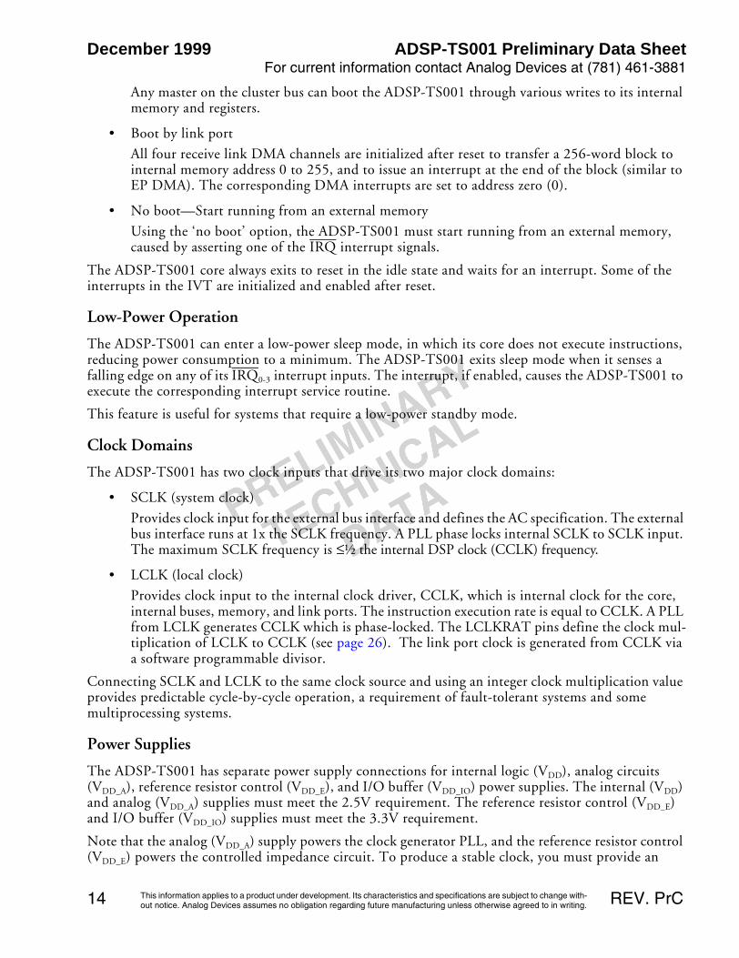
VDD_A Filter
This is the supply for the PLLs.
VDD_A = 2.5V ±5%. The value need not necessarily be the same as VDD; however, it can be derived from VDD by filtering.
Figure 5 shows a possible filtering scheme for VDD_A.
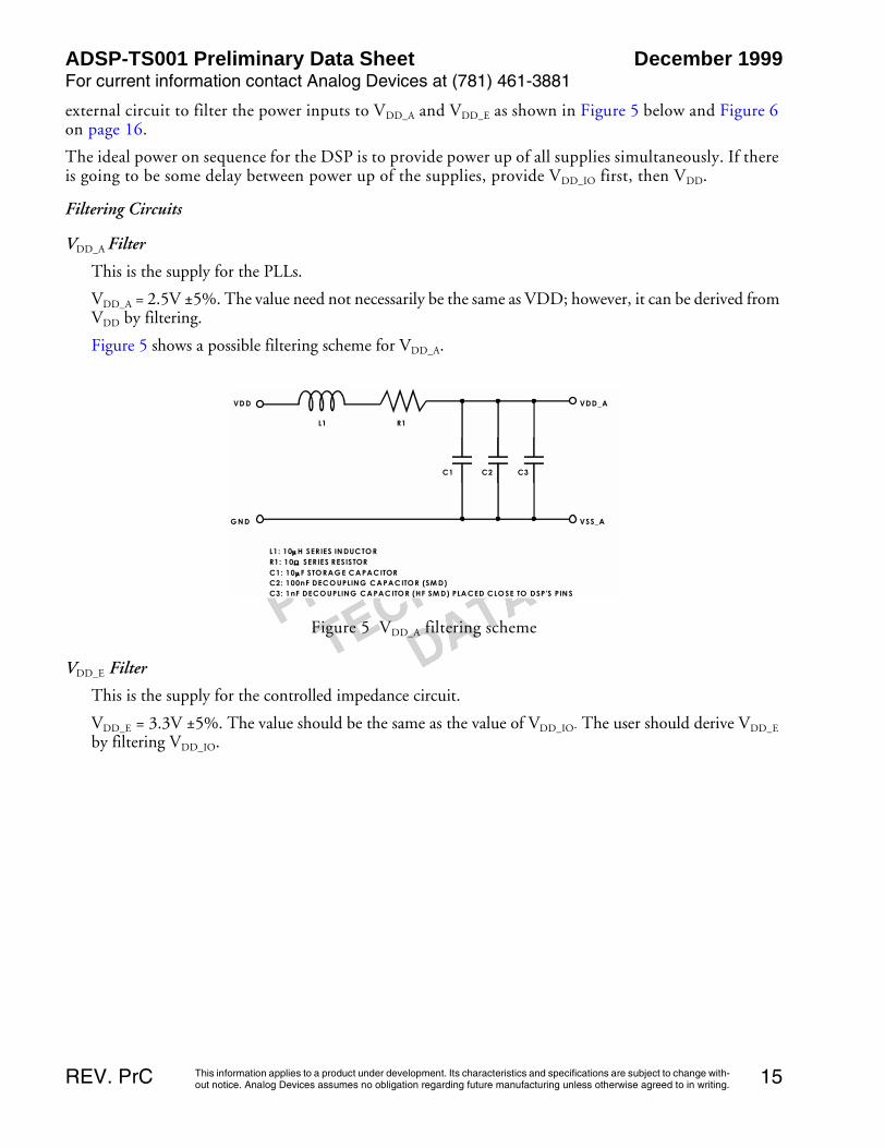
VDD_E Filter
This is the supply for the controlled impedance circuit.
VDD_E = 3.3V ±5%. The value should be the same as the value of VDD_IO. The user should derive VDD_E by filtering VDD_IO.
VDD
L1 R1
C1 C2 C3
VDD_A
VSS_AGN D
L1: 10µµµµ H SERIES IN DUCTORR1: 10ΩΩΩΩ SERIES RESISTORC1: 10 µµµµ F STORAG E CA PAC ITORC2: 100nF DECOUPLING CA PAC ITOR (SM D)C3: 1nF DECOUPLING CA PAC ITOR (HF SM D) PLA CED CLOSE TO DSP'S PIN S
Figure 5 VDD_A filtering scheme
December 1999 ADSP-TS001 Preliminary Data SheetFor current information contact Analog Devices at (781) 461-3881
This information applies to a product under development. Its characteristics and specifications are subject to change with-out notice. Analog Devices assumes no obligation regarding future manufacturing unless otherwise agreed to in writing.16 REV. PrC
Figure 6 shows the filtering scheme for VDD_E.
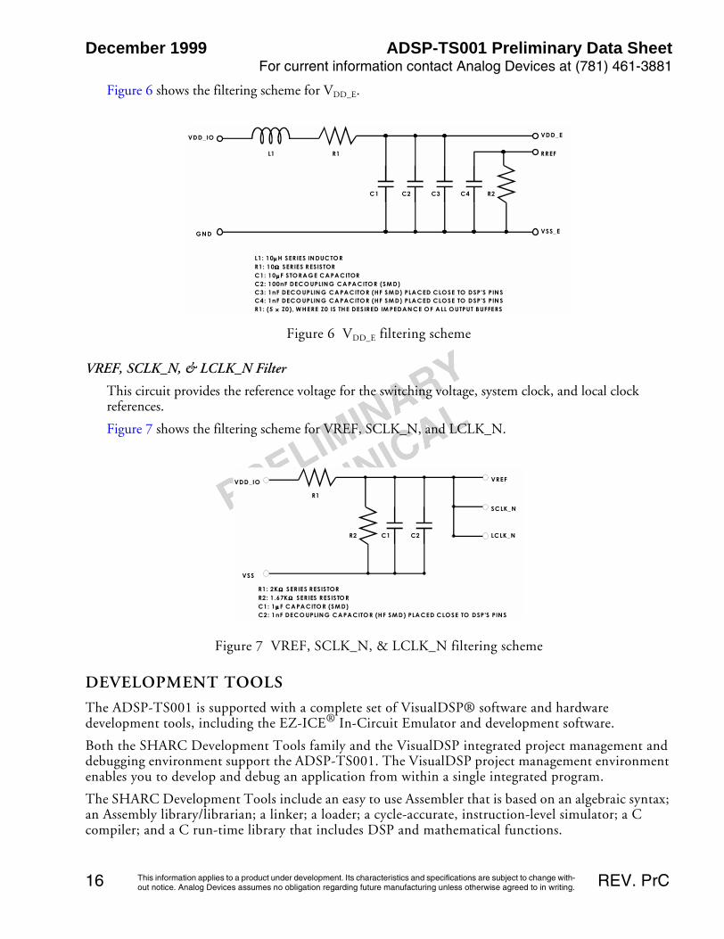
VREF, SCLK_N, & LCLK_N Filter
This circuit provides the reference voltage for the switching voltage, system clock, and local clock references.
Figure 7 shows the filtering scheme for VREF, SCLK_N, and LCLK_N.
DEVELOPMENT TOOLS
The ADSP-TS001 is supported with a complete set of VisualDSP® software and hardware development tools, including the EZ-ICE® In-Circuit Emulator and development software.
Both the SHARC Development Tools family and the VisualDSP integrated project management and debugging environment support the ADSP-TS001. The VisualDSP project management environment enables you to develop and debug an application from within a single integrated program.
The SHARC Development Tools include an easy to use Assembler that is based on an algebraic syntax; an Assembly library/librarian; a linker; a loader; a cycle-accurate, instruction-level simulator; a C compiler; and a C run-time library that includes DSP and mathematical functions.
VDD_IO
L1 R1
C1 C2 C3
VDD_E
VSS_EGN D
L1: 10µµµµ H SERIES IN DUC TORR1: 10ΩΩΩΩ SERIES RESISTORC1: 10µµµµ F STORA GE CA PA CITORC2: 100nF DECO UPLIN G CA PA CITOR (SM D)C3: 1nF DECO UPLIN G CA PA CITOR (HF SM D) PLA CED CLOSE TO DSP'S PIN SC4: 1nF DECO UPLIN G CA PA CITOR (HF SM D) PLA CED CLOSE TO DSP'S PIN SR1: (5 ×××× Z0), W HERE Z0 IS THE DESIRED IM PEDAN CE OF A LL OUTPUT BUFFERS
C4 R2
RREF
Figure 6 VDD_E filtering scheme
VDD_IO
R1
R2 C1 C2
VREF
VSS
R1: 2K ΩΩΩΩ SERIES RESISTORR2: 1 .67K ΩΩΩΩ SERIES RESISTORC1: 1 µµµµ F CA PA CITO R (SM D)C2: 1nF DECO UPLIN G CA PA CITO R (HF SM D) PLA CED CLOSE TO DSP'S PIN S
SCLK_N
LCLK_N
Figure 7 VREF, SCLK_N, & LCLK_N filtering scheme

This information applies to a product under development. Its characteristics and specifications are subject to change with-out notice. Analog Devices assumes no obligation regarding future manufacturing unless otherwise agreed to in writing.
ADSP-TS001 Preliminary Data Sheet December 1999For current information contact Analog Devices at (781) 461-3881
17REV. PrC
Debugging both C and Assembly programs with the VisualDSP debugger, you can:
• View mixed C and Assembly code.
• Insert break points.
• Set conditional breakpoints on registers, memory, and stacks.
• Trace instruction execution.
• Profile program execution.
• Fill and dump memory.
• Source level debugging.
• Create custom debugger windows.
The VisualDSP IDE lets you define and manage DSP software development. Its dialog boxes and property pages enable you to configure and manage all of the SHARC Development Tools, including the syntax highlighting in the VisualDSP editor. This capability lets you:
• Control how the development tools process inputs and generate outputs.
• Maintain a one-to-one correspondence with the tool’s command line switches.
The EZ-ICE Emulator uses the IEEE 1149.1 JTAG test access port of the ADSP-TS001 processor to monitor and control the target board processor during emulation. The EZ-ICE provides full-speed emulation, allowing inspection and modification of memory, registers, and processor stacks. Non-intrusive in-circuit emulation is assured by the use of the processor’s JTAG interface—the emulator does not affect target system loading or timing.
In addition to the software and hardware development tools available from Analog Devices, third parties provide a wide range of tools supporting the SHARC processor family. Hardware tools include SHARC PC plug-in cards, multiprocessor SHARC VME boards, and daughter and modules with multiple SHARCs’ and additional memory. These modules are based on the SHARCPAC module specification. Third Party software tools include DSP libraries, real-time operating systems, and block diagram design tools.
ADDITIONAL INFORMATION
This data sheet provides a general overview of the ADSP-TS001’s architecture and functionality. For detailed information on the ADSP-TS001’s core architecture and instruction set, see the TigerSHARC DSP Hardware Specification. For detailed information on the development tools for this processor, see the VisualDSP User’s Guide and Reference for the ADSP-TS001TigerSHARC DSP.

December 1999 ADSP-TS001 Preliminary Data SheetFor current information contact Analog Devices at (781) 461-3881
This information applies to a product under development. Its characteristics and specifications are subject to change with-out notice. Analog Devices assumes no obligation regarding future manufacturing unless otherwise agreed to in writing.18 REV. PrC
PIN FUNCTION DESCRIPTIONS
While most of the ADSP-TS001’s input pins are normally synchronous—tied to a specific clock—a few are asynchronous. For these asynchronous signals, an on-chip synchronization circuit prevents metastability problems.
The output pins can be three-stated during normal operation. The DSP three-states all outputs during reset, allowing these pins to get to their internal pullup or pulldown state. Unused inputs may be left unconnected (floating). Some output pins (control signals) have a pullup or pulldown that maintain a known value during transitions between different drivers. Open drain outputs have a strong pullup (5KΩ) so they can operate as a wired-OR function.
Table 2. Pin definitions—clocks
Signal Type Description
LCLK_N I Local Clock Reference. Connect this pin to VREF as shown in Figure 7.
LCLK_P I Local Clock Input.
DSP clock input. The instruction cycle rate = n x LCLK, where n is user-programmable to 2, 2.5, 3, 3.5, 4 or 5. LCLK cannot be halted, changed, or operated below the specified frequency.
SCLK_N I System Clock Reference. Connect this pin to VREF as shown in Figure 7.
SCLK_P I System Clock Input.
The DSP’s system input clock for cluster bus.
A = asynchronous; G = ground; I = input; O = output; o/d = open drain output; P = power supply; pd = internal pulldown 100 KΩ; pu = internal pullup 100 KΩ; S = synchronous; T = Three-State
Table 3. Pin definitions—external port
Signal Type Description
ADDR31-0 I/O/T Address Bus.
The DSP issues addresses for accessing memory and peripherals on these pins. In a multiprocessor system, the bus master outputs addresses for accessing internal memory or IOP registers of other ADSP-TS001s. The DSP inputs addresses when a host or another DSP accesses its internal mem-ory or IOP registers.
DATA63-0 I/O/T External Data Bus.
The DSP drives and receives data and instructions on these pins. Pull-up resistors on unused DATA pins are unnecessary.
RD I/O/T (pu) Memory Read.
RD is asserted whenever the DSP reads from any slave in the system, excluding SDRAM. When the DSP is a slave, RD is an input and indicates read transactions that access its internal memory or Uregs. In a multiprocessor system, the bus master drives RD. RD changes concurrently with ADDR pins.
WRL I/O/T (pu) Write Low.
WRL is asserted in two cases: When the ADSP-TS001 writes to an even address word of external memory or to another external bus agent; and when the ADSP-TS001 writes to a 32-bit zone (Host, Memory or DSP programmed to 32-bit bus). An external master (host or DSP) asserts WRL for writing to a DSP’s low word of internal memory. In a multiprocessor system, the bus master drives WRL. WRL changes concurrently with ADDR pins.
A = asynchronous; G = ground; I = input; O = output; o/d = open drain output; P = power supply; pd = internal pulldown 100 KΩ; pu = internal pullup 100 KΩ; S = synchronous; T = Three-State

This information applies to a product under development. Its characteristics and specifications are subject to change with-out notice. Analog Devices assumes no obligation regarding future manufacturing unless otherwise agreed to in writing.
ADSP-TS001 Preliminary Data Sheet December 1999For current information contact Analog Devices at (781) 461-3881
19REV. PrC
WRH I/O/T (pu) Write High.
WRH is asserted when the ADSP-TS001 writes a long word (64 bits) or writes to an odd address word of external memory or to another external bus agent on a 64-bit data bus. An external master (host or another DSP) must assert WRH for writing to a DSP’s high word of 64-bit data bus. In a multiprocessing system, the bus master drives WRH. WRH changes concurrently with ADDR pins.
BMS I/O/T(pu/pd)
Boot Memory Select.
BMS is chip select for boot EPROM or flash memory. During reset, the DSP uses BMS as a strap pin for EPROM boot mode. When the DSP is configured to boot from EPROM, BMS is active during the boot sequence. Pulldown enabled during reset (asserted); pullup enabled after reset (deasserted).
In a multiprocessor system, the DSP bus master drives BMS.
For details see “Reset and Booting” on page 13 and the EBOOT signal on page 26. At reset this is a strap pin, for more information, see Table 9.
MS 1-0 O/T (pu) Memory Select.
MS0 or MS1 is asserted whenever the DSP accesses memory banks 0 or 1 respectively. MS1-0 are decoded memory address pins that change concurrently with ADDR pins:
MS0: ADDR31:26 = 0b000010
MS1: ADDR31:26 = 0b000011
In multiprocessor systems, the master DSP drives MS1-0.
MSH O/T (pu) Memory Select Host.
MSH is asserted whenever the DSP accesses the host address space (ADDR31:28 ≠ 0b0000). MSH is a decoded memory address pin that changes concurrently with ADDR pins.
In a multiprocessor system, the bus master DSP drives MSH.
HBR I Host Bus Request.
A host must assert HBR to request control of the DSP’s external bus. When HBR is asserted in a multiprocessing system, the bus master relinquishes the bus and asserts HBG once the outstanding transaction is finished.
When relinquishing the bus, the master DSP three-states the ADDR31-0, DATA63-0, MSH, MSSD, MS1-0, RD, WRL, WRH, BMS, BRST, FLYBY, IOEN, RAS, CAS, SDWE, SDCKE, LDQM and HDQM pins, and puts the SDRAM in self-refresh mode.
HBG I/O/T (pu) Host Bus Grant.
Acknowledges HBR and indicates that the host can take control of the external bus. The DSP asserts HBG until the host deasserts HBR. In multiprocessor systems, the current bus master DSP drives HBG, and all slave DSPs monitor it.
ACK I/O/T (pu) Acknowledge.
External devices can de-assert ACK to add wait states to external memory accesses. ACK is used by I/O devices, memory controllers and other peripherals on the data phase. The DSP can de-assert ACK to add wait states to synchronous accesses of its internal memory.
CPA I/0/A (o/d) Core Priority Access.
Asserted while the DSP’s core accesses external memory. This pin enables a slave DSP to interrupt a master DSP’s background DMA transfers and gain control of the external bus for core-initiated transactions. CPA is an open drain output, connected to all DSPs in the system.
The CPA pin has an internal 5 KΩ pullup resistor, which is only enabled on the DSP with ID=0. If not required in the system, leave CPA unconnected.
Table 3. Pin definitions—external port (Cont’d)
Signal Type Description
A = asynchronous; G = ground; I = input; O = output; o/d = open drain output; P = power supply; pd = internal pulldown 100 KΩ; pu = internal pullup 100 KΩ; S = synchronous; T = Three-State
December 1999 ADSP-TS001 Preliminary Data SheetFor current information contact Analog Devices at (781) 461-3881
This information applies to a product under development. Its characteristics and specifications are subject to change with-out notice. Analog Devices assumes no obligation regarding future manufacturing unless otherwise agreed to in writing.20 REV. PrC
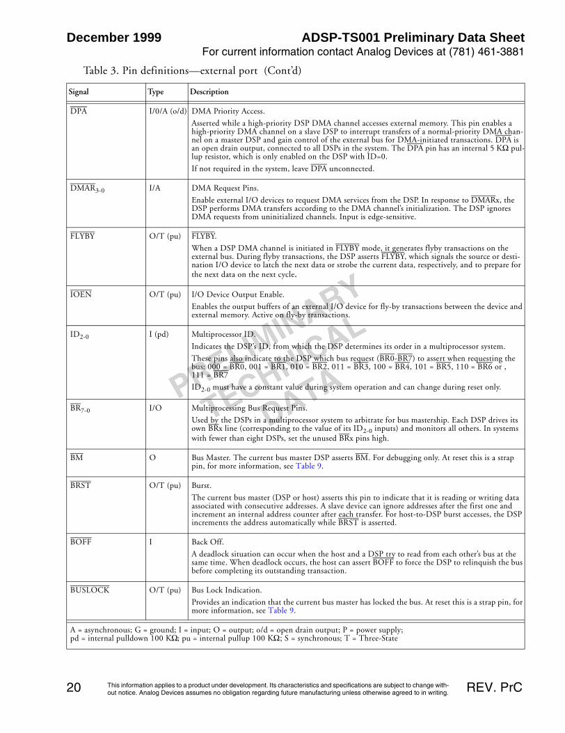
DPA I/0/A (o/d) DMA Priority Access.
Asserted while a high-priority DSP DMA channel accesses external memory. This pin enables a high-priority DMA channel on a slave DSP to interrupt transfers of a normal-priority DMA chan-nel on a master DSP and gain control of the external bus for DMA-initiated transactions. DPA is an open drain output, connected to all DSPs in the system. The DPA pin has an internal 5 KΩ pul-lup resistor, which is only enabled on the DSP with ID=0.
If not required in the system, leave DPA unconnected.
DMAR3-0 I/A DMA Request Pins.
Enable external I/O devices to request DMA services from the DSP. In response to DMARx, the DSP performs DMA transfers according to the DMA channel’s initialization. The DSP ignores DMA requests from uninitialized channels. Input is edge-sensitive.
FLYBY O/T (pu) FLYBY.
When a DSP DMA channel is initiated in FLYBY mode, it generates flyby transactions on the external bus. During flyby transactions, the DSP asserts FLYBY, which signals the source or desti-nation I/O device to latch the next data or strobe the current data, respectively, and to prepare for the next data on the next cycle.
IOEN O/T (pu) I/O Device Output Enable.
Enables the output buffers of an external I/O device for fly-by transactions between the device and external memory. Active on fly-by transactions.
ID2-0 I (pd) Multiprocessor ID.
Indicates the DSP’s ID, from which the DSP determines its order in a multiprocessor system.
These pins also indicate to the DSP which bus request (BR0-BR7) to assert when requesting the bus: 000 = BR0, 001 = BR1, 010 = BR2, 011 = BR3, 100 = BR4, 101 = BR5, 110 = BR6 or , 111 = BR7
ID2-0 must have a constant value during system operation and can change during reset only.
BR7-0 I/O Multiprocessing Bus Request Pins.
Used by the DSPs in a multiprocessor system to arbitrate for bus mastership. Each DSP drives its own BRx line (corresponding to the value of its ID2-0 inputs) and monitors all others. In systems with fewer than eight DSPs, set the unused BRx pins high.
BM O Bus Master. The current bus master DSP asserts BM. For debugging only. At reset this is a strap pin, for more information, see Table 9.
BRST O/T (pu) Burst.
The current bus master (DSP or host) asserts this pin to indicate that it is reading or writing data associated with consecutive addresses. A slave device can ignore addresses after the first one and increment an internal address counter after each transfer. For host-to-DSP burst accesses, the DSP increments the address automatically while BRST is asserted.
BOFF I Back Off.
A deadlock situation can occur when the host and a DSP try to read from each other’s bus at the same time. When deadlock occurs, the host can assert BOFF to force the DSP to relinquish the bus before completing its outstanding transaction.
BUSLOCK O/T (pu) Bus Lock Indication.
Provides an indication that the current bus master has locked the bus. At reset this is a strap pin, for more information, see Table 9.
Table 3. Pin definitions—external port (Cont’d)
Signal Type Description
A = asynchronous; G = ground; I = input; O = output; o/d = open drain output; P = power supply; pd = internal pulldown 100 KΩ; pu = internal pullup 100 KΩ; S = synchronous; T = Three-State
This information applies to a product under development. Its characteristics and specifications are subject to change with-out notice. Analog Devices assumes no obligation regarding future manufacturing unless otherwise agreed to in writing.
ADSP-TS001 Preliminary Data Sheet December 1999For current information contact Analog Devices at (781) 461-3881
21REV. PrC
Table 4. Pin definitions—JTAG
Signal Type Description
EMU O (o/d) Emulation.
Connected to the DSP’s EZ-ICE target board connector only.
TCK I Test Clock (JTAG).
Provides an asynchronous clock for JTAG boundary scan.
TDI I (pu) Test Data Input (JTAG).
A serial data input of the boundary scan path. TDI has a 100 KΩ internal pullup resistor.
TDO O Test Data Output (JTAG).
A serial data output of the boundary scan path.
TMS I (pu) Test Mode Select (JTAG).
Used to control the test state machine. TMS has a 100 KΩ internal pullup resistor.
TRST I/A (pu) Test Reset (JTAG).
Resets the test state machine. TRST must be asserted after power up for proper JTAG operation. TRST has a 100 K Ω internal pullup resistor.
A = asynchronous; G = ground; I = input; O = output; o/d = open drain output; P = power supply; pd = internal pulldown 100 KΩ; pu = internal pullup 100 KΩ; S = synchronous; T = Three-State
Table 5. Pin definitions—link ports
Signal Type Description
L0DAT7-0 I/O Link0 Data7-0
L1DAT7-0 I/O Link1 Data7-0
L2DAT7-0 I/O Link2 Data7-0
L3DAT7-0 I/O Link3 Data7-0
L0CLKOUT O Link0 Clock/Acknowledge Output
L1CLKOUT O Link1 Clock/Acknowledge Output
L2CLKOUT O Link2 Clock/Acknowledge Output
L3CLKOUT O Link3 Clock/Acknowledge Output
L0CLKIN I Link0 Clock/Acknowledge Input
L1CLKIN I Link1 Clock/Acknowledge Input
L2CLKIN I Link2 Clock/Acknowledge Input
L3CLKIN I Link3 Clock/Acknowledge Input
A = asynchronous; G = ground; I = input; O = output; o/d = open drain output; P = power supply; pd = internal pulldown 100 KΩ; pu = internal pullup 100 KΩ; S = synchronous; T = Three-State
December 1999 ADSP-TS001 Preliminary Data SheetFor current information contact Analog Devices at (781) 461-3881
This information applies to a product under development. Its characteristics and specifications are subject to change with-out notice. Analog Devices assumes no obligation regarding future manufacturing unless otherwise agreed to in writing.22 REV. PrC
L0DIR O Link0 Direction.
0 = input
1 = output
At reset this is a strap pin, for more information, see Table 9.
L1DIR O Link1 Direction.
0 = input
1 = output
At reset this is a strap pin, for more information, see Table 9.
L2DIR O Link2 Direction.
0 = input
1 = output
At reset this is a strap pin, for more information, see Table 9.
L3DIR O Link3 Direction.
0 = input
1 = output
At reset this is a strap pin, for more information, see Table 9.
L0FSY I/O Link0 Frame Synchronization.
When asserted by the link master, LxFSY indicates completion of the frame.
L1FSY I/O Link1 Frame Synchronization.
When asserted by the link master, LxFSY indicates completion of the frame.
L2FSY I/O Link2 Frame Synchronization.
When asserted by the link master, LxFSY indicates completion of the frame.
L3FSY I/O Link3 Frame Synchronization.
When asserted by the link master, LxFSY indicates completion of the frame.
Table 5. Pin definitions—link ports (Cont’d)
Signal Type Description
A = asynchronous; G = ground; I = input; O = output; o/d = open drain output; P = power supply; pd = internal pulldown 100 KΩ; pu = internal pullup 100 KΩ; S = synchronous; T = Three-State

This information applies to a product under development. Its characteristics and specifications are subject to change with-out notice. Analog Devices assumes no obligation regarding future manufacturing unless otherwise agreed to in writing.
ADSP-TS001 Preliminary Data Sheet December 1999For current information contact Analog Devices at (781) 461-3881
23REV. PrC
Table 6. Pin definitions—power, ground, and reference
Signal Type Description
CONTROLIMP2-0 I (pd) Impedance Control.
Every group of outputs has two controls:res_cont 0 = maximum drive pulse
1 = matched resistancepulse 0 = continuously matched impedance
1 = 2ns pulse for max resistance at the beginning of the transitionFor ADC (Address/Data/Controls) and LINK (all link port outputs) signals:
CONTROLIMP ADC LINKres_cont pulse res_cont pulse
000 0 X 0 X001 0 X 0 X010 0 X 1 0011 0 X 1 1100 1 0 0 X
101 1 1 0 X110 1 0 1 0111 1 1 1 1
VDD P Vdd Pins for internal logic.
VDD_A1 P Vdd Pins for analog circuits.
VDD_E1 P VDD pin for reference resistor control.
VDD_IO P Vdd pins for I/O buffers.
VREF I Reference voltage defines the trip point for all input buffers (which are TTL-compatible).
The value is 1.5V ± 100mv (which is the TTL trip point).
VREF can be connected to a power supply or set by a voltage divider circuit. The voltage divider should have an HF decoupling capacitor (prepared 1nF HF SND) connected to VSS. Tie the decoupling capacitor between VREF input and VSS, as close to the DSP’s pins as possible.
RREF I Reference resistor tied between RREF and VSS_E.
For PCB, the value should be five times the value of matched resistance required for PCB traces. For example, if the target impedance is 50Ω, place a 250Ω resistor between RREF and VSS_E.
Also, tie a decoupling capacitor (prepared 1nF HF SND) between RREF and VSS_E, as close to the DSP’s pins as possible.
VSS G Ground Pins.
VSS_A G Ground Pins for analog circuits.
VSS_E P VSS pin for reference resistor control.
A = asynchronous; G = ground; I = input; O = output; o/d = open drain output; P = power supply; pd = internal pulldown 100 KΩ; pu = internal pullup 100 KΩ; S = synchronous; T = Three-State
1. For details on deriving filtering circuits with the VDD_A and VDD_E pins, see “Filtering Circuits” on page 15.

December 1999 ADSP-TS001 Preliminary Data SheetFor current information contact Analog Devices at (781) 461-3881
This information applies to a product under development. Its characteristics and specifications are subject to change with-out notice. Analog Devices assumes no obligation regarding future manufacturing unless otherwise agreed to in writing.24 REV. PrC
Table 7. Pin definitions—flag I/O, IRQ, reset, and timer
Signal Type Description
FLAG3-0 I/O/A (pd) FLAG pins.
Bidirectional input/output pins. Each pin can be configured individually for input or for output. FLAG3-0 are inputs after power-up and reset. These pins are held at zero (0) value by a static 100KΩ pulldown resistor.
IRQ3-0 I/A (pu) Interrupt Request.
When asserted, the DSP generates an interrupt. Each of the IRQ3-0 pins can be independently set for edge-triggered or level-sensitive operation.
After reset, these pins are disabled unless the IRQ strap option and interrupt vectors are initialized for booting.
RESET I/A Reset.
Sets the DSP to a known state and causes program fetch to start at an address specified by the reset vector register. RESET must be asserted a specified time according to the type of reset operation. For details, see “Reset and Booting” on page 13.
TMR0E O Timer 0 expires.
This output pulses for four cycles whenever timer 0 expires. At reset this is a strap pin, for more information, see Table 9.
A = asynchronous; G = ground; I = input; O = output; o/d = open drain output; P = power supply; pd = internal pulldown 100 KΩ; pu = internal pullup 100 KΩ; S = synchronous; T = Three-State
Table 8. Pin definitions—SDRAM
Signal Type Description
CAS_A I/O/T (pu) Column Address Select A.
When sampled low at rising edge of the clock, CAS indicates that a column address is valid in a read or write of SDRAM. In other SDRAM accesses, it defines the type of operation to execute according to the SDRAM specification.
CAS_B O/T (pu) Column Address Select B.
Duplication of CAS_A for drive strength, output only.
HDQM_A O/T (pd) High Word SDRAM Data Mask A.
When sampled high, three-states the SDRAM DQ buffers. HDQM_A is valid on SDRAM transac-tions when CAS is asserted, and inactive on read transactions. On write transactions, HDQM_A is active when accessing an even address in word accesses or when memory is configured for a 32-bit bus to disable the write of the high word..
HDQM_B O/T (pd) High Word SDRAM Data Mask B.
Duplication of HDQM_A for drive strength, output only.
LDQM_A O/T (pd) Low Word SDRAM Data Mask A.
When sampled high, three-states the SDRAM DQ buffers. LDQM_A is valid on SDRAM transac-tions when CAS is asserted, and inactive on read transactions. On write transactions, LDQM_A is active when accessing an odd address word on a 64-bit memory bus to disable the write of the low word.
LDQM_B O/T (pd) Low Word SDRAM Data Mask B.
Duplication of LDQM_A for drive strength, output only.
A = asynchronous; G = ground; I = input; O = output; o/d = open drain output; P = power supply; pd = internal pulldown 100 KΩ; pu = internal pullup 100 KΩ; S = synchronous; T = Three-State

This information applies to a product under development. Its characteristics and specifications are subject to change with-out notice. Analog Devices assumes no obligation regarding future manufacturing unless otherwise agreed to in writing.
ADSP-TS001 Preliminary Data Sheet December 1999For current information contact Analog Devices at (781) 461-3881
25REV. PrC
MSSD_A I/O/T (pu) Memory Select SDRAM A.
MSSD is asserted whenever the DSP accesses SDRAM memory space. MSSD is a decoded memory address pin that is asserted whenever the DSP issues an SDRAM command cycle (access to ADDR31:26 = 0b000001). In a multiprocessor system, the master DSP drives MSSD.
MSSD_B O/T (pu) High Word SDRAM Data Mask B.
Duplication of MSSD_A for drive strength, output only.
RAS_A I/O/T (pu) Row Address Select A.
When sampled low at the rising edge of the clock, RAS indicates that a row address is valid in a read or write of SDRAM. In other SDRAM accesses, it defines the type of operation to execute accord-ing to SDRAM specification.
RAS_B O/T (pu) Row Address Select B.
Duplication of RAS_A for drive strength, output only.
SDA10_A O/T (pu) SDRAM A10_A.
SDRAM Address bit 10 pin. Separate A10 signals enable SDRAM refresh operation while the DSP executes non-SDRAM transactions.
SDA10_B O/T (pu) SDRAM A10_B.
Duplication of SDA10_A for drive strength, output only.
SDCKE_A I/O/T(pu/pd)
SDRAM Clock Enable A.
Activates the SDRAM clock for SDRAM self-refresh or suspend modes. A slave DSP in a multipro-cessor system does not have the pullup or pulldown. A master DSP (or ID=0 in a single processor system) has a 100 KΩ pullup before granting the bus to the host, except when the SDRAM is put in self refresh mode. In self refresh mode, the master has a 100 KΩ pulldown before granting the bus to the host.
SDCKE_B O/T(pu/pd)
SDRAM Clock Enable B.
Duplication of SDCKE_A for drive strength, output only. A slave DSP in a multiprocessor system does not have the pullup or pulldown. A master DSP (or ID=0 in a single processor system) has a 100 KΩ pullup before granting the bus to the host, except when the SDRAM is put in self refresh mode. In self refresh mode, the master has a 100 KΩ pulldown before granting the bus to the host.
SDWE_A I/O/T (pu) SDRAM Write Enable A.
When sampled low at rising edge of the clock and CAS is active, SDWE_A indicates an SDRAM write access. When sampled high at rising edge of the clock and CAS is active, SDWE_A indicates an SDRAM read access. In other SDRAM accesses, SDWE_A defines the type of operation to exe-cute according to SDRAM specification.
SDWE_B O/T (pu) SDRAM Write Enable B.
Duplication of SDWE_A for drive strength, output only.
Table 8. Pin definitions—SDRAM (Cont’d)
Signal Type Description
A = asynchronous; G = ground; I = input; O = output; o/d = open drain output; P = power supply; pd = internal pulldown 100 KΩ; pu = internal pullup 100 KΩ; S = synchronous; T = Three-State

December 1999 ADSP-TS001 Preliminary Data SheetFor current information contact Analog Devices at (781) 461-3881
This information applies to a product under development. Its characteristics and specifications are subject to change with-out notice. Analog Devices assumes no obligation regarding future manufacturing unless otherwise agreed to in writing.26 REV. PrC
Some pins have another function at reset. Strap options set DSP operating modes. During reset, the DSP samples the strap option pins. Strap pins have a 100 KΩ pull-down for the default value. If a strap pin is not connected to an external pull-up or logic load, the DSP samples the default value during reset. To set a mode other than the default mode, connect the strap pin to a 10 KΩ external pull-up. Table 9 lists and describes each of the DSP’s strap pins. If strap pins are used as drivers to logic inputs, a 4.7 KΩ pulldown or pullup is required.
Table 9. I/O Strap Pins
Signal On Pin… Description
DLL_BYPASS TMR0E Timer 0 Output Bypass.
0 = DLL works normally (default)
1 = If set during reset, SCLK input bypasses the DLL and connects directly to the DSP’s internal I/O clock
EBOOT BMS EPROM boot.
0 = boot from EPROM immediately after reset (default)
1 = idle after reset and wait for an external device to boot DSP through the external port or a link port
In systems that do not boot from an EPROM, short BMS to VDD_IO or (to retain access to flash memory) connect BMS to VDD_IO with a pullup resistor.
IRQEN BM Interrupt Enable.
0 = disable and set IRQ interrupts to level-sensitive after reset (default)
1 = enable and set IRQ interrupts to edge-sensitive immediately after reset
LCLKRAT2-0 L0DIRL1DIRL2DIR
LCLK Ratio.
The DSP’s core clock (instruction cycle rate) = n × LCLK, where n is user-programmable to 2, 2.5, 3, 3.5, 4, or 5.
Ratio LCLKRAT2 LCLKRAT1 LCLKRAT0
2 0 0 02.5 0 0 13 0 1 03.5 0 1 14 1 0 05 1 0 1
PLL_BYPASS BUSLOCK Bus Lock Bypass.
0 = PLL works normally (default)
1 = If set during rest, LCLK input bypasses the PLL and connects directly to the DSP’s internal core clock
SCLKFREQ L3DIR SCLK Frequency.
Indicates to the SCLK deskew PLL the SCLK frequency range.
0 = 50 to 100 MHz (default)
1 = <50 MHz

This information applies to a product under development. Its characteristics and specifications are subject to change with-out notice. Analog Devices assumes no obligation regarding future manufacturing unless otherwise agreed to in writing.
ADSP-TS001 Preliminary Data Sheet December 1999For current information contact Analog Devices at (781) 461-3881
27REV. PrC
DESIGNING AN EZ-ICE COMPATIBLE SYSTEM
This application note describes how to design the interface between an Analog Devices JTAG DSP and the emulation header on a custom DSP target board. The environment described uses an Analog Devices (ADI) SHARC DSP as an example. However, this information is applicable for all of ADI's JTAG DSPs.
The White Mountain DSP-Analog Devices family of emulators are tools that every DSP developer needs to test and debug their hardware and software system. ADI has supplied an IEEE 1149.1 JTAG Test Access Port (TAP) on each JTAG DSP. The emulator uses the TAP to access the internals of the DSP, allowing the developer to load code, set breakpoints, observe variables, observe memory, examine registers, etc. The DSP must be halted to send data and commands, but once an operation is completed by the emulator, the DSP system is set running at full speed with no impact on system timing.
The last thing an engineer wants to do when testing a new hardware design is debug the emulation port of their target board. Since the emulation port in many cases is the only vehicle to test a new target board, it needs to work flawlessly. The guidelines set forth in this application note are designed to help eliminate possible JTAG emulation port problems.
Target Board Connector
The emulator interface to an ADI JTAG DSP is a 14-pin header, as shown in Figure 8. The customer must supply this header on their target board in order to communicate with the emulator. The interface consists of a standard dual row 0.025" square post header, set on 0.1" x 0.1" spacing, with a minimum post length of 0.235". Pin 3 is the key position used to prevent the pod from being inserted backwards. This pin must be clipped on the target board.
Also, the clearance (length, width, and height) around the header must be considered. Leave a clearance of at least 0.15” and 0.10” around the length and width of the header, and reserve a height clearance to attach and detach the pod connector. See “White Mountain DSP Pod Designs” on page 31 for detailed drawings of the pod connector.
Figure 8 Emulator Interface for ADI JTAG DSPs
As shown in Figure 8, the interface has two sets of signals on the header. The standard JTAG signals TMS, TCK, TDI, TDO, TRST, EMU, and SCLK_P are used for emulation purposes (via an emulator). Secondary JTAG signals BTMS, BTCK, BTRST, and BTDI are used for optional board-level (boundary scan) testing. These "B" signals would connect to a separate on-board JTAG

December 1999 ADSP-TS001 Preliminary Data SheetFor current information contact Analog Devices at (781) 461-3881
This information applies to a product under development. Its characteristics and specifications are subject to change with-out notice. Analog Devices assumes no obligation regarding future manufacturing unless otherwise agreed to in writing.28 REV. PrC
boundary scan controller if used. Most customers will never use the "B" signals. If these signals are not used, tie all of them to ground, except BTCK. Pull BTCK up to VDD_IO (VCC in Figure 9) using a 4.7KΩ resistor, as shown in Figure 9.
When the emulator is not connected to this header, place jumpers across BTMS, BTCK, BTRST, and BTDI as shown in Figure 9. This holds the JTAG signals in the correct state to allow the DSP to run freely. Remove all the jumpers when connecting the emulator to the JTAG header.
Figure 9 JTAG target board connector with no local boundary scan (VCC=VDD_IO)
Table 10 lists the state of each standard JTAG signal.
The CLKIN signal is the clock signal line that connects to all DSPs (typically 30 MHz or greater). For synchronous DSP operation to work correctly, the CLKIN signal on all DSPs must be the same signal and the skew between them must be minimal—see the TigerSHARC DSP Hardware Specification for more details on CLKIN.
Table 10. State of Standard JTAG Signals
Signal Description Emulator DSP
TMS Test Mode Select O I
TCK Test Clock (10 MHz) O I
TRST Test Reset O I
TDI Test Data In O I
TDO Test Data Out I O
EMU Emulation Pin I I/O (Open Drain)
CLKIN (Optional) DSP Clock Input I I
I = input; I/O = input/output; O = output

This information applies to a product under development. Its characteristics and specifications are subject to change with-out notice. Analog Devices assumes no obligation regarding future manufacturing unless otherwise agreed to in writing.
ADSP-TS001 Preliminary Data Sheet December 1999For current information contact Analog Devices at (781) 461-3881
29REV. PrC
Note that the CLKIN signal presently is not used by the emulator and can cause noise problems if connected to the JTAG header. If you are experiencing noise from this signal, clip this pin on the 14-pin JTAG header, or, since the CLKIN signal is not used by the emulator, simply tie the CLKIN pin to ground on the 14-pin JTAG header (do not connect it to the DSP’s CLKIN signal).
The final connections between a single DSP target and the emulation header (within 6 inches) are shown in Figure 10. A 4.7KΩ pull-up resistor has been added on TCK, TDI, and TMS for increased noise resistance.
Figure 10 Single DSP Connection to JTAG Header (VCC=VDD_IO)
Should your design use more than one DSP (or other JTAG device in the scan chain), or if your JTAG header is more than 6 inches from the DSP, use a buffered connection scheme as shown in Figure 11 (no local boundary scan mode shown). Using a buffer that has built in series resistors such as the 74ABT2244 family can help reduce ringing on the JTAG signal lines. For low voltage applications (3.3V), the 74ALVT, and 74AVC logic families are a good starting point. Also, note the position of the pull-up resistor on EMU. This is required since the EMU line is an open drain signal.

December 1999 ADSP-TS001 Preliminary Data SheetFor current information contact Analog Devices at (781) 461-3881
This information applies to a product under development. Its characteristics and specifications are subject to change with-out notice. Analog Devices assumes no obligation regarding future manufacturing unless otherwise agreed to in writing.30 REV. PrC
Important: If you have more than one DSP (or JTAG device) on your target (in the scan chain), it is imperative that you buffer the JTAG header. Buffering keeps the signals clean and avoids noise problems that occur with longer signal traces.
Figure 11 Multiple DSP Connection to JTAG Header (VCC=VDD_IO)
Although the theoretical number of devices that can be supported (by the software) in one JTAG scan chain is quite large (50 devices or more), we recommended that you use no more than eight physical devices in one scan chain. (A physical device could however contain many JTAG devices such as inside a multichip module). This recommendation is due mostly to the transmission line effects that appear in long signal traces and is based on some field-collected empirical data. For large numbers of physical devices, the best approach is to break the chain into several smaller independent chains, each with their own JTAG header and buffer. If this is not possible, at least add some jumpers that can reduce the number of devices in one chain for debug purposes, and pay special attention in the layout stage for transmission line effects.
Layout Requirements
All JTAG signals (TCK, TMS, TDI, TDO, EMU, TRST, CLKIN) should be treated as critical route signals. This means paying special attention when you route these signals. Specify a controlled impedance requirement for each route (value depends on your circuit board—typically 50-75Ω). Keep crosstalk and inductance to a minimum on these lines by using a good ground plane and by routing away from other high noise signals, such as clock lines. Keep these routes as short and clean as possible, and keep the bused signals (TMS, TCK, TRST, EMU) as close to the same length as possible.
Power Sequence
The power-on sequence for your target and emulation system is as follows:
1. Apply power to the emulator first, then to the target board.
This ensures that the JTAG signals are in the correct state for the DSP to run free.
Upon power-on, the emulator drives the TRST signal low, keeping the DSP TAP in the test-logic-reset state, until the emulation software takes control.
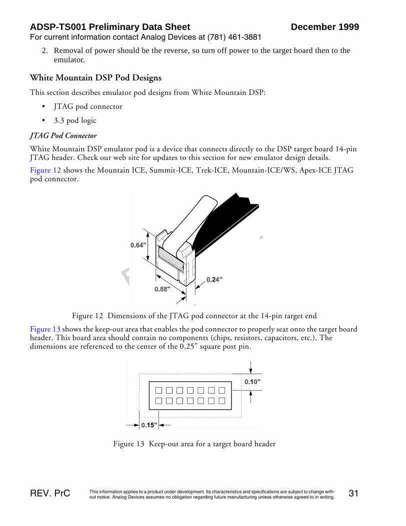
This information applies to a product under development. Its characteristics and specifications are subject to change with-out notice. Analog Devices assumes no obligation regarding future manufacturing unless otherwise agreed to in writing.
ADSP-TS001 Preliminary Data Sheet December 1999For current information contact Analog Devices at (781) 461-3881
31REV. PrC
2. Removal of power should be the reverse, so turn off power to the target board then to the emulator.
White Mountain DSP Pod Designs
This section describes emulator pod designs from White Mountain DSP:
• JTAG pod connector
• 3.3 pod logic
JTAG Pod Connector
White Mountain DSP emulator pod is a device that connects directly to the DSP target board 14-pin JTAG header. Check our web site for updates to this section for new emulator design details.
Figure 12 shows the Mountain ICE, Summit-ICE, Trek-ICE, Mountain-ICE/WS, Apex-ICE JTAG pod connector.
Figure 12 Dimensions of the JTAG pod connector at the 14-pin target end
Figure 13 shows the keep-out area that enables the pod connector to properly seat onto the target board header. This board area should contain no components (chips, resistors, capacitors, etc.). The dimensions are referenced to the center of the 0.25” square post pin.
Figure 13 Keep-out area for a target board header

December 1999 ADSP-TS001 Preliminary Data SheetFor current information contact Analog Devices at (781) 461-3881
This information applies to a product under development. Its characteristics and specifications are subject to change with-out notice. Analog Devices assumes no obligation regarding future manufacturing unless otherwise agreed to in writing.32 REV. PrC
3.3V Pod Logic
A portion of the White Mountain DSP 3.3V emulator pod interface is shown in Figure 14. This figure describes the driver circuitry of the emulator pod. As can be seen, TMS, TCK, TRST, and TDI are driven with a 10Ω series resistor. TDO and CLKIN are terminated with an optional 91/120Ω parallel terminator. EMU is pulled up with a 4.7KΩ resistor. The 74LVT244 chip drives the signals at 3.3V, with a maximum current rating of ±32mA.
Figure 14 shows the Mountain ICE, Summit-ICE, Trek-ICE, Mountain-ICE/WS, Apex-ICE 3.3V JTAG pod driver logic.
Figure 14 3.3V JTAG pod driver logic (VCC=VDD_IO)
If needed, you can parallel terminate the TMS, TCK, TRST, and TDI lines locally on your target board since these signals are driven by the pod with sufficient current drive (±32mA). To use the terminators on the TDO and CLKIN lines, you must have a buffer on your target board JTAG header and CLKIN signal. The DSP is incapable of driving the parallel terminator load directly with TDO. Assuming you have the proper buffers, to use the optional parallel terminators, just place a jumper on J2 or J3.

This information applies to a product under development. Its characteristics and specifications are subject to change with-out notice. Analog Devices assumes no obligation regarding future manufacturing unless otherwise agreed to in writing.
ADSP-TS001 Preliminary Data Sheet December 1999For current information contact Analog Devices at (781) 461-3881
33REV. PrC
ADSP-TS001—SPECIFICATIONS
Note that component specifications are subject to change without notice.
Table 11. Recommended operating conditions
Parameter Test ConditionsK Grade
UnitMin Max
VDDInternal Supply Voltage 2.375 2.625 V
VDD_A Analog Supply Voltage1
1. For details on deriving filtering circuits with the VDD_A and VDD_E pins, see “Filtering Circuits” on page 15.
2.375 2.625 V
VDD_IOI/O Supply Voltage 3.15 3.45 V
VDD_E Reference Resistor Supply Voltage1 3.15 3.45 V
TCASECase Operating Temperature 0 +85 oC
VIHHigh-Level Input Voltage2
2. Applies to input and bidirectional pins: ACK, ADDR31-0, BOFF, BR7-0, CAS_A, CONTROLIMP2-0, CPA, DATA63-0, DMAR3-0,DPA, FLAG3-0, HBG, ID2-0, IRQ3-0, L0DAT7-0, L1DAT7-0, L2DAT7-0, L0CLKOUT, L1CLKOUT, L2CLKOUT, L3CLKOUT,L0CLKIN, L1CLKIN, L2CLKIN, L3CLKIN, L0FSY, L1FSY, L2FSY, L3FSY, LCLK_P, LCLK_N, MSSD_A, RAS_A, RD, RESET,SCLK_P, SCLK_IN, SDWE_A, TDI, TMS, TCK, TRST, WRL, WRH.
@ VDD = max 2 VDD + 0.5 V
VILLow-Level Input Voltage2 @ VDD = min −0.5 0.8 V
VREFVoltage reference 1.4 1.6 V
Table 12 ABSOLUTE MAXIMUM RATINGS1
1. Stresses greater than those listed above may cause permanent damage to the device. These are stress ratings only, and functional oper-ation of the device at these or any other conditions greater than those indicated in the operational sections of this specification is notimplied. Exposure to absolute maximum rating conditions for extended periods may affect device reliability.
Parameter Absolute Maximum Rating
Internal (Core) Supply Voltage (VDD) -0.3 V to +3.0 V
Reference Resistor Supply Voltage (VDD_E) -0.3 V to +4.6 V
Analog (PLL) Supply Voltage (VDD_A) -0.3 V to +3.0 V
External (I/O) Supply Voltage (VDD_IO) -0.3 V to +4.6 V
Input Voltage -0.5 V to VDD_IO + 0.5 V
Output Voltage Swing -0.5 V to VDD_IO + 0.5 V
Load Capacitance 200 pF
Storage Temperature Range -65°C to +150°C
Lead Temperature (5 seconds) TBD °C

December 1999 ADSP-TS001 Preliminary Data SheetFor current information contact Analog Devices at (781) 461-3881
This information applies to a product under development. Its characteristics and specifications are subject to change with-out notice. Analog Devices assumes no obligation regarding future manufacturing unless otherwise agreed to in writing.34 REV. PrC
ESD Sensitivity
Table 13. Electrical characteristics
Parameter Test ConditionsK GradesMinMax Units
VOH High-Level Output Voltage1 @ VDD = min, IOH = -2 uA 2.4 V
VOL Low-Level Output Voltage1 @ VDD = min, IOL = 4 uA 0.4 V
IIH High-Level Input Current2, 3 @ VDD = max, VIN = VDD max 10 uA
IIL Low-Level Input Current2 @ VDD = max, VIN = 0V6 10 uA
IILPLow-Level Input Current3 @ VDD = max, VIN = 0V6 A
IOZH Three-State Leakage Current4, 5, 7 @ VDD = max, VIN = VDD max 10 uA
IOZL Three-State Leakage Current 4, 6 @ VDD = max, VIN = 0V 10 uA
IOZHPThree-State Leakage Current6 @ VDD = max, VIN = VDD max A
IOZLOThree-State Leakage Current7 @ VDD = max, VIN = 0V A
IOZLSThree-State Leakage Current5 @ VDD = max, VIN = 0V A
CINInput Capacitance8, 9 fIN = 1MHz, TCASE = 25C, VIN = 2.5V F
1. Applies to output and bidirectional pins: ACK, ADDR31-0, BM, BMS, BUSLOCK, BR7-0, BRST, CAS_A, CAS_B, DATA63-0, DP,EMU, FLAG3-0, FLYBY, HBG, IHDQM_A, HDQM_B, IOEN, L0DAT7-0, L1DAT7-0, L2DAT7-0, L0CLKOUT, L1CLKOUT,L2CLKOUT, L3CLKOUT, L0CLKIN, L1CLKIN, L2CLKIN, L3CLKIN, L0DIR, L1DIR, L2DIR, L3DIR, L0FSY, L1FSY, L2FSY,L3FSY, LDQM_A, LDQM_B, MS1-0, MSSD_A, RAS_A, RAS_B, RD, SDA10_A, SDA10_B, SDCKE_A, SDCKE_B, SDWE_A,SDWE_B, TDO, TMROE, WRL, WRH.
2. Applies to input pins: BOFF, CONTROLIMP2-0, DMAR3-0, HBR, ID2-0, LCLK_P, LCLK_N, RESET, SCLK_P, SCLK_N, TCK.3. Applies to input pins with internal pullups: IRQ3-0, TDI, TMS, TRST.4. Applies to three-stateable pins: ADDR31-0, BUSLOCK, DATA63-0, SDA10_A, SDA10_B.5. Applies to three-stateable pins with internal pullups: ACK, BRST, BMS, CAS_A, CAS_B, FLYBY, HBG, IOEN, MS1-0, MSH,
MSSD_A, MSSD_B, RAS_A, RAS_B, RD, SDWE_A, SDWE_B, WRL, WRH.6. Applies to three-stateable pins with internal pulldowns: FLAG3-0, HDQM_A, HDQM_B, LDQM_A., LDQM_B, SDCKE_A,
SDCKE_B.7. Applies to open drain pins with 5KΩ pull ups: CPA, DPA.8. Applies to all signals.9. Guaranteed but not tested.
CAUTION: ESD (electrostatic discharge) sensitive device. Electrostatic charges as high as 4000V readily accumulate on the human body and test equipment and can discharge with-out detection. Although the ADSP-TS001 features proprietary ESD protection circuitry, permanent damage may occur on devices subjected to high-energy electrostatic discharges. Therefore, proper ESD precautions are recommended to avoid performance degradation or loss of functionality.

Pages 35 through 48 of this document cover timing and pinout for
the ADSP-TS001. These pages are only available to registered Tig-
erSHARC customers. Please contact DSP product support at:
(with the subject: TigerSHARC Timing Info)
to request timing and pinout information.
For other TigerSHARC documentation, register through the
Analog Devices DSP website at:
www.analog.com/dsp