Embed Size (px)
Citation preview
1
1HJ94, Spring 2005, Ingrid Verbauwhede, les 8
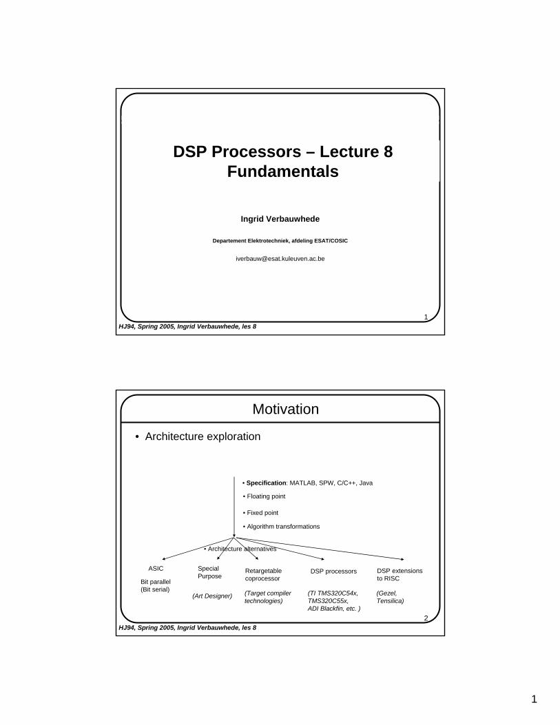
DSP Processors – Lecture 8Fundamentals
Ingrid Verbauwhede
Departement Elektrotechniek, afdeling ESAT/COSIC
2HJ94, Spring 2005, Ingrid Verbauwhede, les 8
Motivation
• Architecture exploration
• Specification: MATLAB, SPW, C/C++, Java
• Floating point
• Fixed point
• Algorithm transformations
• Architecture alternatives
Bit parallel (Bit serial)
ASIC SpecialPurpose
(Art Designer)
Retargetablecoprocessor
(Target compilertechnologies)
DSP extensionsto RISC
DSP processors
(Gezel,Tensilica)
(TI TMS320C54x,TMS320C55x,ADI Blackfin, etc. )
2
3HJ94, Spring 2005, Ingrid Verbauwhede, les 8
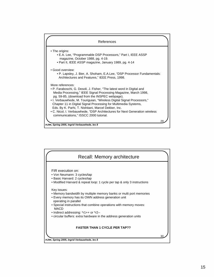
References
• The origins:• E.A. Lee, “Programmable DSP Processors,” Part I, IEEE ASSP
magazine, October 1988, pg. 4-19.• Part II, IEEE ASSP magazine, January 1989, pg. 4-14
• Good overview:• P. Lapsley, J. Bier, A. Shoham, E.A.Lee, “DSP Processor Fundamentals:
Architectures and Features,” IEEE Press, 1998.
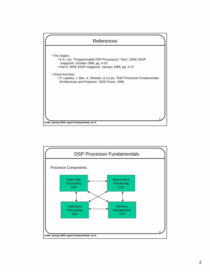
4HJ94, Spring 2005, Ingrid Verbauwhede, les 8
DSP Processor Fundamentals
Data PathProcessing
Unit
InterconnectProcessing
Unit
MemoryManagement
Unit
InstructionProcessing
Unit
Processor Components:
3
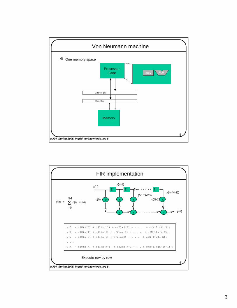
5HJ94, Spring 2005, Ingrid Verbauwhede, les 8
Von Neumann machine
Processor Core
Memory
One memory space
mpy ALU
Address Bus
Data Bus
6HJ94, Spring 2005, Ingrid Verbauwhede, les 8
FIR implementation
x(n)
X
(50 TAPS)
Z-1 Z-1 Z-1
X X X
+ + +
x(n-1)
y(n)
c(0) c(N-1)
x(n-(N-1))
Σy(n) = c(i) x(n-i)N-1
i=0
y(0) = c(0)x(0) + c(1)x(-1) + c(2)x(-2) + . . . + c(N-1)x(1-N);
y(1) = c(0)x(1) + c(1)x(0) + c(2)x(-1) + . . . + c(N-1)x(2-N);
y(2) = c(0)x(2) + c(1)x(1) + c(2)x(0) + . . . + c(N-1)x(3-N);
. . .
y(n) = c(0)x(n) + c(1)x(n-1) + c(2)x(n-2)+ . . + c(N-1)x(n-(N-1));
Execute row by row
4
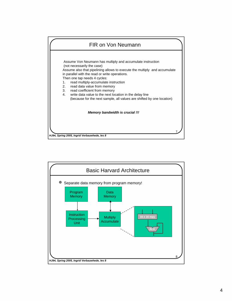
7HJ94, Spring 2005, Ingrid Verbauwhede, les 8
FIR on Von Neumann
Assume Von Neumann has multiply and accumulate instruction(not necessarily the case)
Assume also that pipelining allows to execute the multiply and accumulatein parallel with the read or write operations.Then one tap needs 4 cycles:1. read multiply-accumulate instruction2. read data value from memory3. read coefficient from memory4. write data value to the next location in the delay line
(because for the next sample, all values are shifted by one location)
Memory bandwidth is crucial !!!
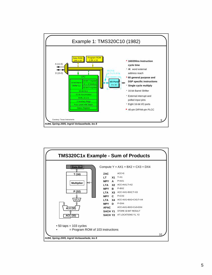
8HJ94, Spring 2005, Ingrid Verbauwhede, les 8
Basic Harvard Architecture
ProgramMemory
DataMemory
MultiplyAccumulate
InstructionProcessing
Unit
Separate data memory from program memory!
16 x 16 mpy
ALU
5
9HJ94, Spring 2005, Ingrid Verbauwhede, les 8
Example 1: TMS320C10 (1982)
Data RAM Program ROM1.5K x 16144 x 16
16-bit T-register
16 x 16 Multiply
32-bit P-register
16-bit BarrelShifter (L)
32-bit ALU
32-bit Accumulator
ShiftL (0,1,4)
2 Auxiliary RegsFour Level H/W Stack
Status Register
CPU
D (15-0)
A (11-0)
I/O Ports8 x 16
PA (7-0)(A 2-0, D 15-0)
160/200ns Instructioncycle time4K word externaladdress reach
60 general purpose andDSP specific instructionsSingle cycle multiply
16-bit Barrel Shifter
External interrupt andpolled input pins
Eight 16-bit I/O ports
40-pin DIP/44-pin PLCC
Courtesy: Texas Instruments
10HJ94, Spring 2005, Ingrid Verbauwhede, les 8
TMS320C1x Example - Sum of Products
MUX
Data Bus
T (16)
Multiplier
P (32)
ALU (32)
ACC (32)
Compute Y = AX1 + BX2 + CX3 + DX4
ZACLTMPYLTAMPYLTAMPYLTAMPYAPACSACHSACH
X1AX2BX3CX4D
Y1Y2
ACC=0
T=X1
P=AX1
ACC=AX1;T=X2
P=BX2
ACC=AX1+BX2;T=X3
P=CX3
ACC=AX1+BX2+CX3;T=X4
P=DX4
ACC=AX1+BX2+Cx3+DX4
STORE 32-BIT RESULT
AT LOCATIONS Y1, Y2
• 50 taps = 103 cycles• = Program ROM of 103 instructions
6
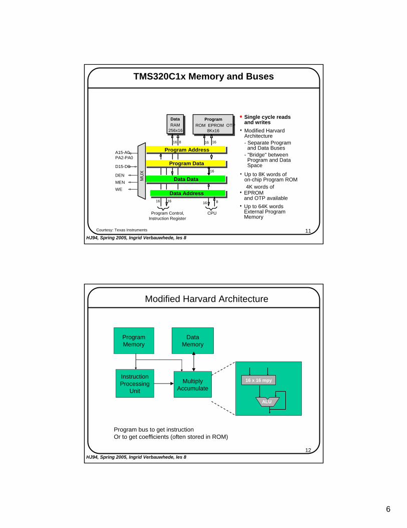
11HJ94, Spring 2005, Ingrid Verbauwhede, les 8
TMS320C1x Memory and Buses
Data Address
Data Data
Instruction Register
Single cycle readsand writesModified HarvardArchitecture- Separate Program
and Data Buses- "Bridge" between
Program and DataSpace
Up to 8K words ofon-chip Program ROM4K words of
EPROMand OTP availableUp to 64K wordsExternal ProgramMemory
DataRAM
256x16
ProgramROM EPROM OTP
8Kx16
Program Address
Program Data
A15-A0,PA2-PA0
D15-D0
DENMENWE
Program Control, CPU
816 16 16
16
8161616
MU
X
Courtesy: Texas Instruments
12HJ94, Spring 2005, Ingrid Verbauwhede, les 8
Modified Harvard Architecture
ProgramMemory
DataMemory
MultiplyAccumulate
InstructionProcessing
Unit
16 x 16 mpy
ALU
Program bus to get instructionOr to get coefficients (often stored in ROM)
7
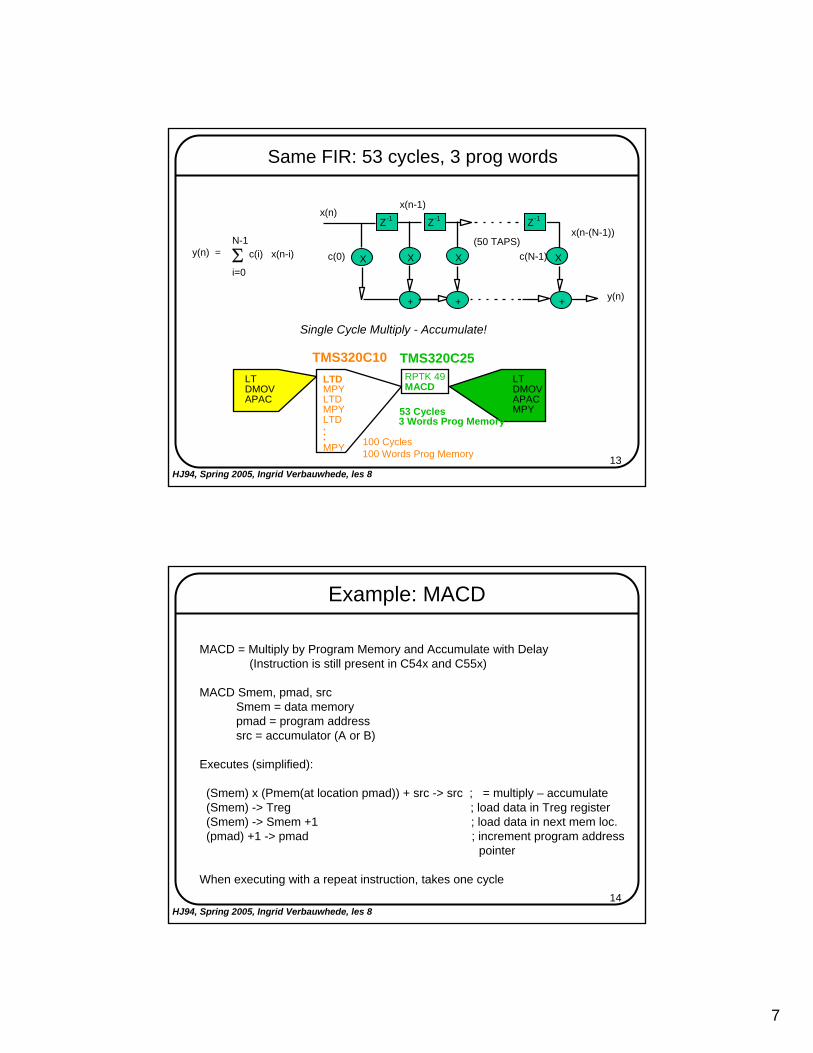
13HJ94, Spring 2005, Ingrid Verbauwhede, les 8
Same FIR: 53 cycles, 3 prog words
x(n)
X
(50 TAPS)
Z-1 Z-1 Z-1
X X X
+ + +
x(n-1)
y(n)
c(0) c(N-1)
x(n-(N-1))
Σy(n) = c(i) x(n-i)N-1
i=0
TMS320C10 TMS320C25LTD RPTK 49MPY MACDLTDMPYLTD
MPY
LTDMOVAPAC
LTDMOVAPACMPY
3 Words Prog Memory53 Cycles
100 Words Prog Memory100 Cycles
...
Single Cycle Multiply - Accumulate!
14HJ94, Spring 2005, Ingrid Verbauwhede, les 8
Example: MACD
MACD = Multiply by Program Memory and Accumulate with Delay(Instruction is still present in C54x and C55x)
MACD Smem, pmad, srcSmem = data memorypmad = program addresssrc = accumulator (A or B)
Executes (simplified):
(Smem) x (Pmem(at location pmad)) + src -> src ; = multiply – accumulate(Smem) -> Treg ; load data in Treg register(Smem) -> Smem +1 ; load data in next mem loc.(pmad) +1 -> pmad ; increment program address
pointer
When executing with a repeat instruction, takes one cycle
8
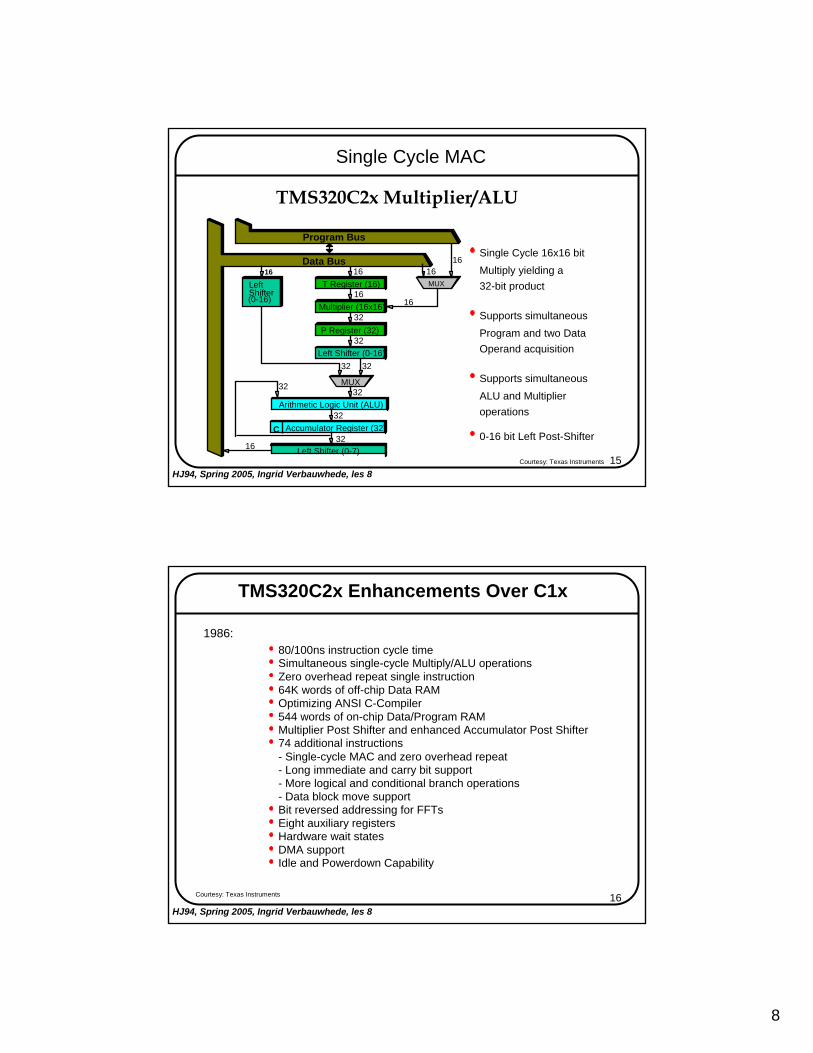
15HJ94, Spring 2005, Ingrid Verbauwhede, les 8
16 16
16
32
32
32
32
32
Single Cycle MAC
TMS320C2x Multiplier/ALU
Left Shifter (0-7)
Left Shifter (0-16)3232
16
Single Cycle 16x16 bitMultiply yielding a32-bit product
Supports simultaneousProgram and two DataOperand acquisition
Supports simultaneousALU and Multiplieroperations
0-16 bit Left Post-Shifter
Data Bus
Program Bus
LeftShifter(0-16)
T Register (16)
Multiplier (16x16)
P Register (32)
MUX
Arithmetic Logic Unit (ALU)
Accumulator Register (32)C
MUX
16
16
16
32
Courtesy: Texas Instruments
16HJ94, Spring 2005, Ingrid Verbauwhede, les 8
TMS320C2x Enhancements Over C1x
Multiplier Post Shifter and enhanced Accumulator Post Shifter
80/100ns instruction cycle timeSimultaneous single-cycle Multiply/ALU operationsZero overhead repeat single instruction64K words of off-chip Data RAMOptimizing ANSI C-Compiler544 words of on-chip Data/Program RAM
74 additional instructions- Single-cycle MAC and zero overhead repeat- Long immediate and carry bit support- More logical and conditional branch operations- Data block move supportBit reversed addressing for FFTsEight auxiliary registersHardware wait statesDMA supportIdle and Powerdown Capability
Courtesy: Texas Instruments
1986:
9
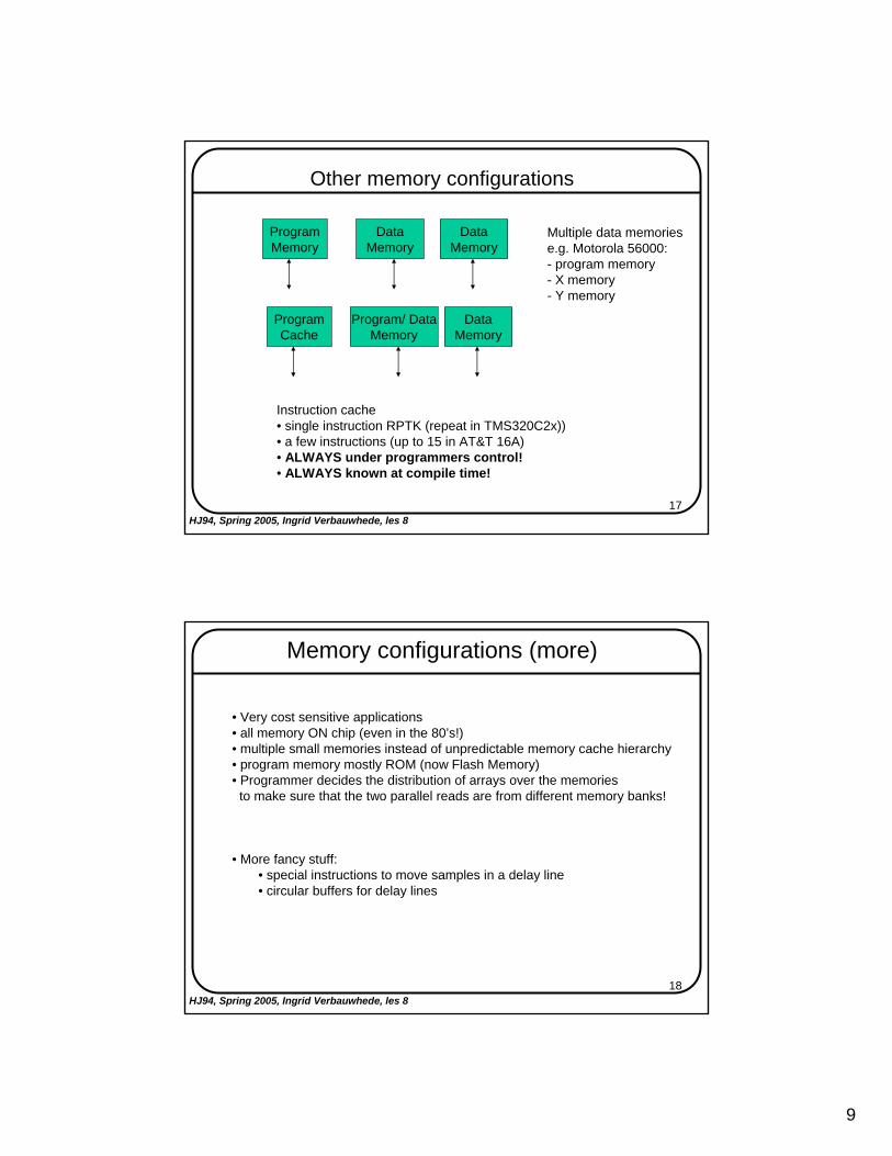
17HJ94, Spring 2005, Ingrid Verbauwhede, les 8
Other memory configurations
ProgramMemory
DataMemory
DataMemory
ProgramCache
Program/ DataMemory
DataMemory
Multiple data memoriese.g. Motorola 56000:- program memory- X memory- Y memory
Instruction cache• single instruction RPTK (repeat in TMS320C2x))• a few instructions (up to 15 in AT&T 16A)• ALWAYS under programmers control!• ALWAYS known at compile time!
18HJ94, Spring 2005, Ingrid Verbauwhede, les 8
Memory configurations (more)
• Very cost sensitive applications• all memory ON chip (even in the 80’s!)• multiple small memories instead of unpredictable memory cache hierarchy• program memory mostly ROM (now Flash Memory) • Programmer decides the distribution of arrays over the memories
to make sure that the two parallel reads are from different memory banks!
• More fancy stuff:• special instructions to move samples in a delay line• circular buffers for delay lines
10
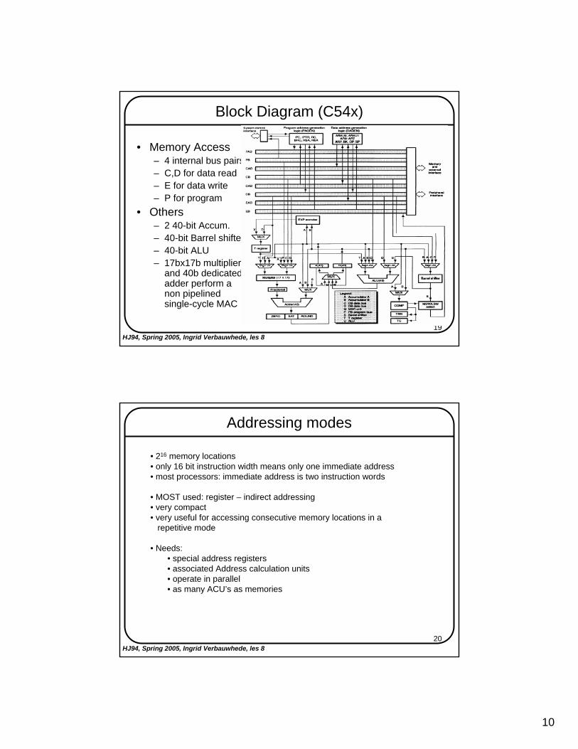
19HJ94, Spring 2005, Ingrid Verbauwhede, les 8
Block Diagram (C54x)
• Memory Access– 4 internal bus pairs– C,D for data read– E for data write– P for program
• Others– 2 40-bit Accum.– 40-bit Barrel shifter– 40-bit ALU– 17bx17b multiplier
and 40b dedicated adder perform a non pipelined single-cycle MAC
20HJ94, Spring 2005, Ingrid Verbauwhede, les 8
Addressing modes
• 216 memory locations• only 16 bit instruction width means only one immediate address• most processors: immediate address is two instruction words
• MOST used: register – indirect addressing• very compact• very useful for accessing consecutive memory locations in a
repetitive mode
• Needs:• special address registers• associated Address calculation units • operate in parallel• as many ACU’s as memories
11
21HJ94, Spring 2005, Ingrid Verbauwhede, les 8
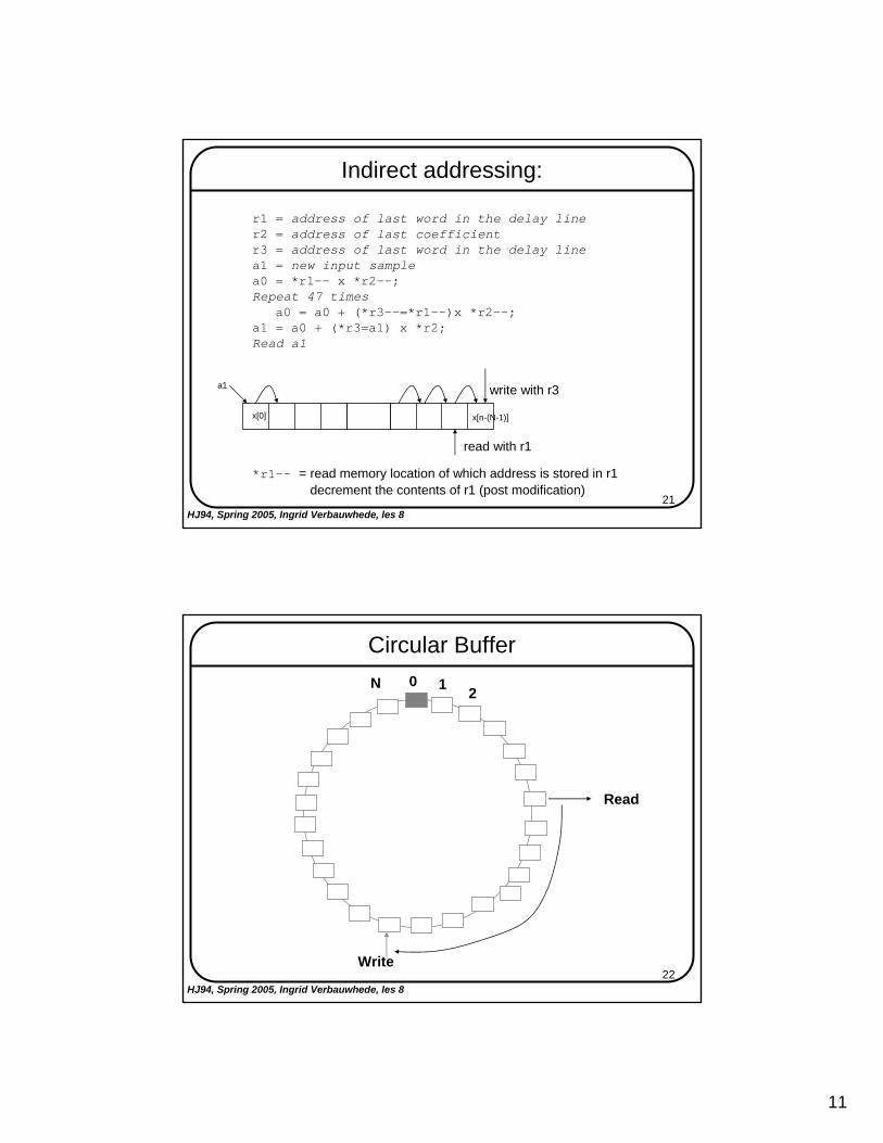
Indirect addressing:
r1 = address of last word in the delay liner2 = address of last coefficientr3 = address of last word in the delay linea1 = new input samplea0 = *r1-- x *r2--;Repeat 47 times
a0 = a0 + (*r3--=*r1--)x *r2--;a1 = a0 + (*r3=a1) x *r2;Read a1
read with r1
write with r3
*r1-- = read memory location of which address is stored in r1decrement the contents of r1 (post modification)
x[n-(N-1)]x[0]
a1
22HJ94, Spring 2005, Ingrid Verbauwhede, les 8
Circular Buffer0 1 2
N
Read
Write
12
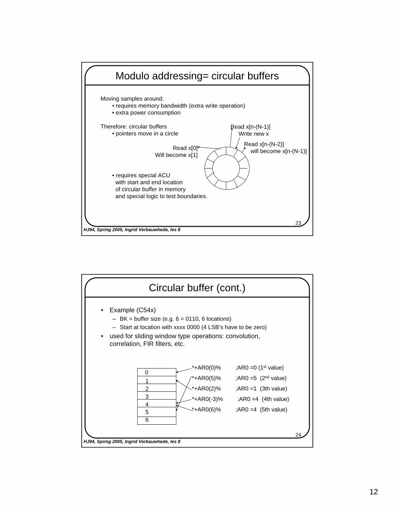
23HJ94, Spring 2005, Ingrid Verbauwhede, les 8
Modulo addressing= circular buffers
Moving samples around:• requires memory bandwidth (extra write operation)• extra power consumption
Therefore: circular buffers• pointers move in a circle
• requires special ACUwith start and end locationof circular buffer in memoryand special logic to test boundaries.
Read x[n-(N-1)]Write new x
Read x[n-(N-2)]will become x[n-(N-1)]Read x[0]
Will become x[1]
24HJ94, Spring 2005, Ingrid Verbauwhede, les 8
Circular buffer (cont.)
• Example (C54x)– BK = buffer size (e.g. 6 = 0110, 6 locations)– Start at location with xxxx 0000 (4 LSB’s have to be zero)
• used for sliding window type operations: convolution, correlation, FIR filters, etc.
*+AR0(0)% ;AR0 =0 (1st value)
*+AR0(5)% ;AR0 =5 (2nd value)
*+AR0(2)% ;AR0 =1 (3th value)
*+AR0(-3)% ;AR0 =4 (4th value)
*+AR0(6)% ;AR0 =4 (5th value)
0123456
13
25HJ94, Spring 2005, Ingrid Verbauwhede, les 8
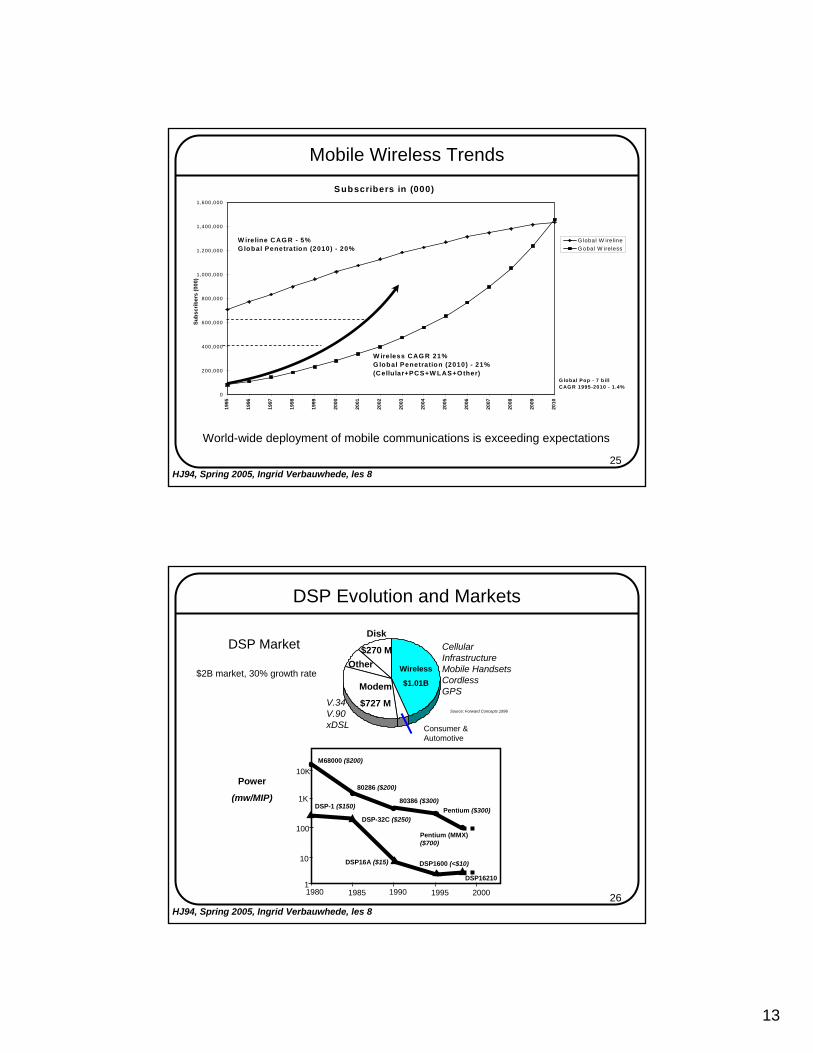
Mobile Wireless Trends
Subscribers in (000)
0
200,000
400,000
600,000
800,000
1,000,000
1,200,000
1,400,000
1,600,000
1995
1996
1997
1998
1999
2000
2001
2002
2003
2004
2005
2006
2007
2008
2009
2010
G lobal W irelineG obal W ireless
W ireless CAG R 21%G lobal Penetration (2010) - 21%(Cellular+PCS+W LAS+O ther)
W ireline CAG R - 5%G lobal Penetration (2010) - 20%
G lobal Pop - 7 b illCAG R 1995-2010 - 1.4%
Subs
crib
ers
(000
)
World-wide deployment of mobile communications is exceeding expectations
26HJ94, Spring 2005, Ingrid Verbauwhede, les 8
DSP Evolution and Markets
Power
(mw/MIP)
1980 1985 1990 1995 2000
DSP-1 ($150)
DSP16A ($15) DSP1600 (<$10)
1K
100
10
10KM68000 ($200)
80286 ($200)
80386 ($300)Pentium ($300)
1
DSP-32C ($250)
DSP16210
Pentium (MMX) ($700)
Cellular InfrastructureMobile HandsetsCordlessGPS
Wireless
$1.01BModem
$727 MV.34V.90xDSL Consumer &
Automotive
Disk
$270 MOther
Source: Forward Concepts 1996
$2B market, 30% growth rate
DSP Market
Power
(mw/MIP)
14
27HJ94, Spring 2005, Ingrid Verbauwhede, les 8
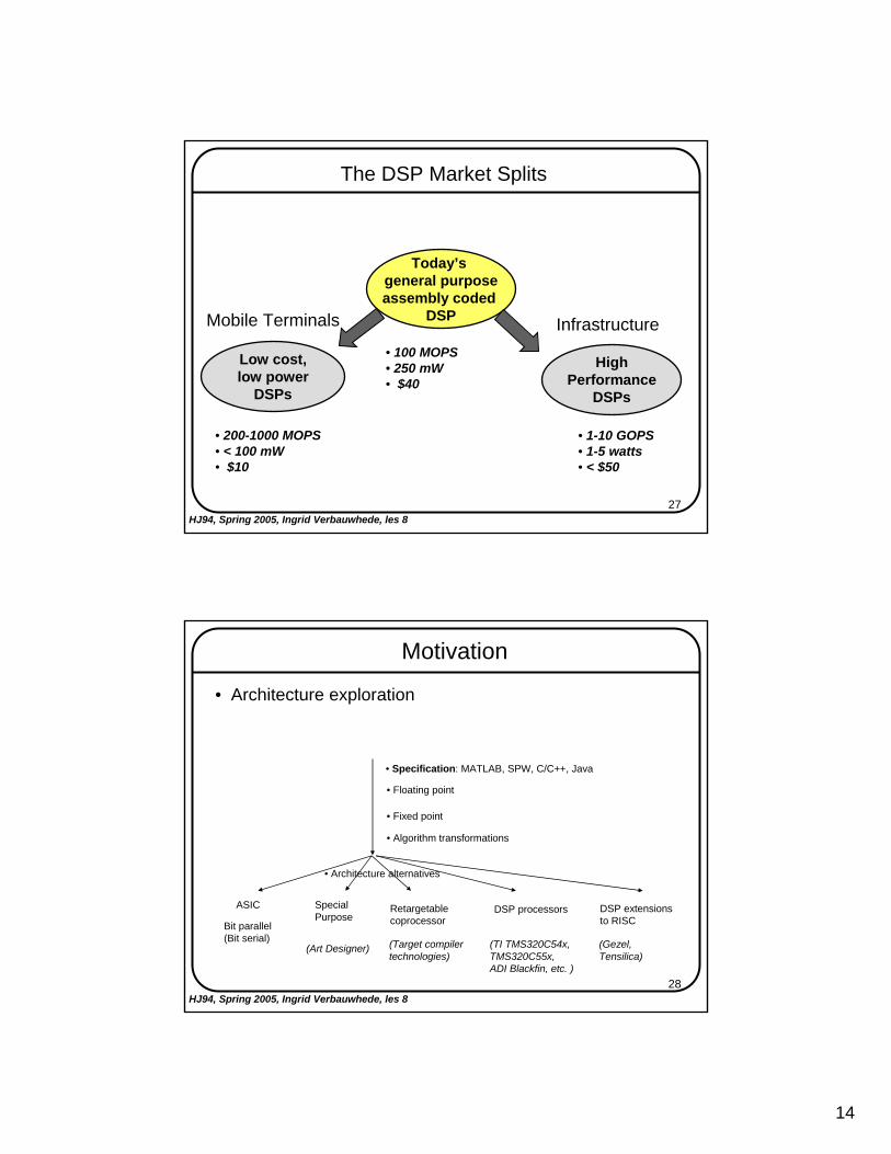
The DSP Market Splits
Today’s general purposeassembly coded
DSP
Low cost,low power
DSPs
HighPerformance
DSPs
• 1-10 GOPS• 1-5 watts• < $50
• 200-1000 MOPS• < 100 mW• $10
• 100 MOPS• 250 mW• $40
InfrastructureMobile Terminals
28HJ94, Spring 2005, Ingrid Verbauwhede, les 8
Motivation
• Architecture exploration
• Specification: MATLAB, SPW, C/C++, Java
• Floating point
• Fixed point
• Algorithm transformations
• Architecture alternatives
Bit parallel (Bit serial)
ASIC SpecialPurpose
(Art Designer)
Retargetablecoprocessor
(Target compilertechnologies)
DSP extensionsto RISC
DSP processors
(Gezel,Tensilica)
(TI TMS320C54x,TMS320C55x,ADI Blackfin, etc. )
15
29HJ94, Spring 2005, Ingrid Verbauwhede, les 8
References
• The origins:• E.A. Lee, “Programmable DSP Processors,” Part I, IEEE ASSP
magazine, October 1988, pg. 4-19.• Part II, IEEE ASSP magazine, January 1989, pg. 4-14
• Good overview:• P. Lapsley, J. Bier, A. Shoham, E.A.Lee, “DSP Processor Fundamentals:
Architectures and Features,” IEEE Press, 1998.
More references:• P. Faraboschi, G. Desoli, J. Fisher, “The latest word in Digital and
Media Processing,” IEEE Signal Processing Magazine, March 1998,pg. 59-85, (download from the INSPEC webpage).
• I. Verbauwhede, M. Touriguian, “Wireless Digital Signal Processors,”Chapter 11 in Digital Signal Processing for Multimedia Systems,Eds. By K. Parhi, T. Nishitani, Marcel Dekker, Inc.
• C. Nicol, I. Verbauwhede, “DSP Architectures for Next Generation wireless communications,” ISSCC 2000 tutorial.
30HJ94, Spring 2005, Ingrid Verbauwhede, les 8
Recall: Memory architecture
FIR execution on:• Von Neumann: 3 cycles/tap• Basic Harvard: 2 cycles/tap• Modified Harvard & repeat loop: 1 cycle per tap & only 3 instructions
Key issues:• Memory bandwidth by multiple memory banks or multi port memories• Every memory has its OWN address generation unit
operating in parallel• Special instructions that combine operations with memory moves:
MACD• Indirect addressing: *r1++ or *r2--• circular buffers: extra hardware in the address generation units
FASTER THAN 1 CYCLE PER TAP??
16
31HJ94, Spring 2005, Ingrid Verbauwhede, les 8
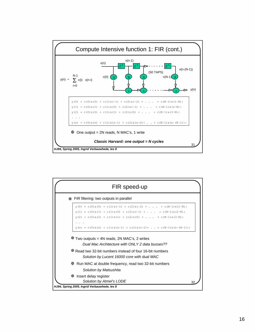
Compute Intensive function 1: FIR (cont.)
x(n)
X
(50 TAPS)
Z-1 Z-1 Z-1
X X X
+ + +
x(n-1)
y(n)
c(0) c(N-1)
x(n-(N-1))
Σy(n) = c(i) x(n-i)N-1
i=0
y(0) = c(0)x(0) + c(1)x(-1) + c(2)x(-2) + . . . + c(N-1)x(1-N);
y(1) = c(0)x(1) + c(1)x(0) + c(2)x(-1) + . . . + c(N-1)x(2-N);
y(2) = c(0)x(2) + c(1)x(1) + c(2)x(0) + . . . + c(N-1)x(3-N);
. . .
y(n) = c(0)x(n) + c(1)x(n-1) + c(2)x(n-2)+ . . + c(N-1)x(n-(N-1));
One output = 2N reads, N MAC’s, 1 write
Classic Harvard: one output = N cycles
32HJ94, Spring 2005, Ingrid Verbauwhede, les 8
FIR speed-up
y(0) = c(0)x(0) + c(1)x(-1) + c(2)x(-2) + . . . + c(N-1)x(1-N);
y(1) = c(0)x(1) + c(1)x(0) + c(2)x(-1) + . . . + c(N-1)x(2-N);
y(2) = c(0)x(2) + c(1)x(1) + c(2)x(0) + . . . + c(N-1)x(3-N);
. . .
y(n) = c(0)x(n) + c(1)x(n-1) + c(2)x(n-2)+ . . + c(N-1)x(n-(N-1));
Run MAC at double frequency, read two 32-bit numbers
FIR filtering: two outputs in parallel
Two outputs = 4N reads, 2N MAC’s, 2 writesDual Mac Architecture with ONLY 2 data busses??
Read two 32-bit numbers instead of four 16-bit numbers Solution by Lucent 16000 core with dual MAC
Solution by Matsushita
Insert delay registerSolution by Atmel’s LODE
17
33HJ94, Spring 2005, Ingrid Verbauwhede, les 8
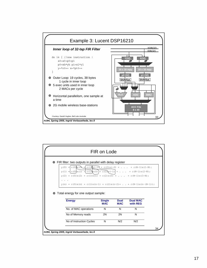
Example 3: Lucent DSP16210
Horizontal parallelism, one sample at a time
2G mobile wireless base-stations
16 x 16 mpy 16 x 16 mpy
p0 (32) p1 (32)
Shift/Sat.
ADD BMU
ACC File8 x 40
Y(32) X(32)
ALU
Shift/Sat.
do 14 { //one instruction !
a0=a0+p0+p1
p0=xh*yh p1=xl*yl
y=*r0++ x=*pt0++
}
Inner loop of 32-tap FIR Filter XDB(32)IDB(32)
Outer Loop: 19 cycles, 38 bytes1 cycle in inner loop
5 exec units used in inner loop2 MACs per cycle
Courtesy: Gareth Hughes, Bell Labs Australia
34HJ94, Spring 2005, Ingrid Verbauwhede, les 8
FIR on Lode
FIR filter: two outputs in parallel with delay register y(0) = c(0)x(0) + c(1)x(-1) + c(2)x(-2) + . . . + c(N-1)x(1-N);
y(1) = c(0)x(1) + c(1)x(0) + c(2)x(-1) + . . . + c(N-1)x(2-N);
y(2) = c(0)x(2) + c(1)x(1) + c(2)x(0) + . . . + c(N-1)x(3-N);
. . .
y(n) = c(0)x(n) + c(1)x(n-1) + c(2)x(n-2)+ . . + c(N-1)x(n-(N-1));
Total energy for one output sample:
Energy SingleMAC
DualMAC
Dual MACwith REG
No. of MAC operations N N N
No of Memory reads 2N 2N N
No of Instruction Cycles N N/2 N/2
18
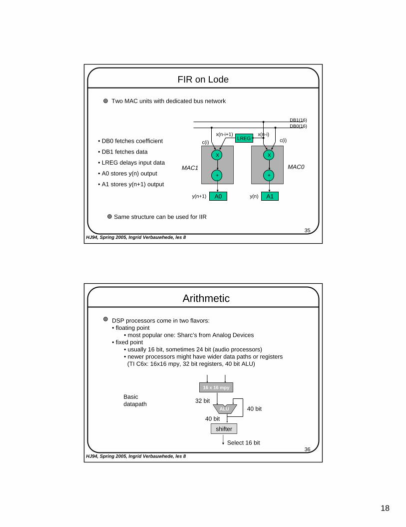
35HJ94, Spring 2005, Ingrid Verbauwhede, les 8
FIR on Lode
Two MAC units with dedicated bus network
x(n-i)
X
LREG
+
y(n+1) y(n)
c(i)
X
+
c(i)x(n-i+1)
A0 A1
MAC1 MAC0
DB1(16)DB0(16)
• DB0 fetches coefficient
• DB1 fetches data
• LREG delays input data
• A0 stores y(n) output
• A1 stores y(n+1) output
Same structure can be used for IIR
36HJ94, Spring 2005, Ingrid Verbauwhede, les 8
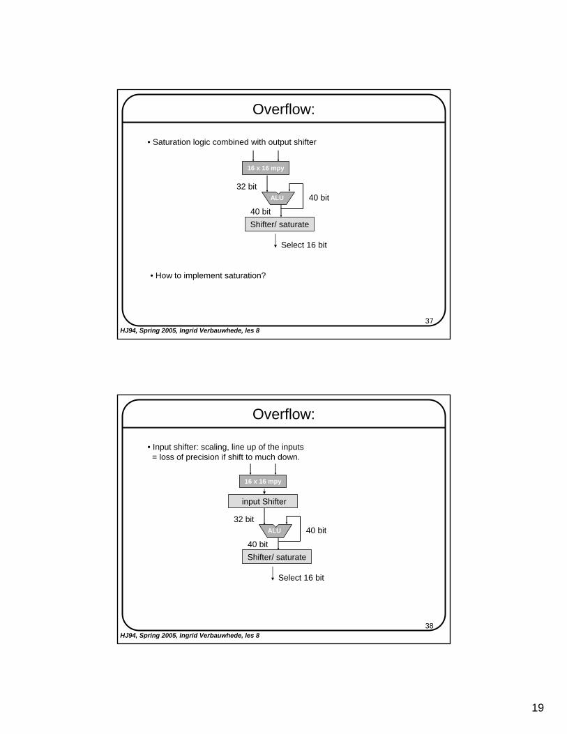
Arithmetic
DSP processors come in two flavors:• floating point
• most popular one: Sharc’s from Analog Devices• fixed point
• usually 16 bit, sometimes 24 bit (audio processors)• newer processors might have wider data paths or registers
(TI C6x: 16x16 mpy, 32 bit registers, 40 bit ALU)
16 x 16 mpy
ALU32 bit
40 bit
shifter
Select 16 bit
40 bit
Basic datapath
19
37HJ94, Spring 2005, Ingrid Verbauwhede, les 8
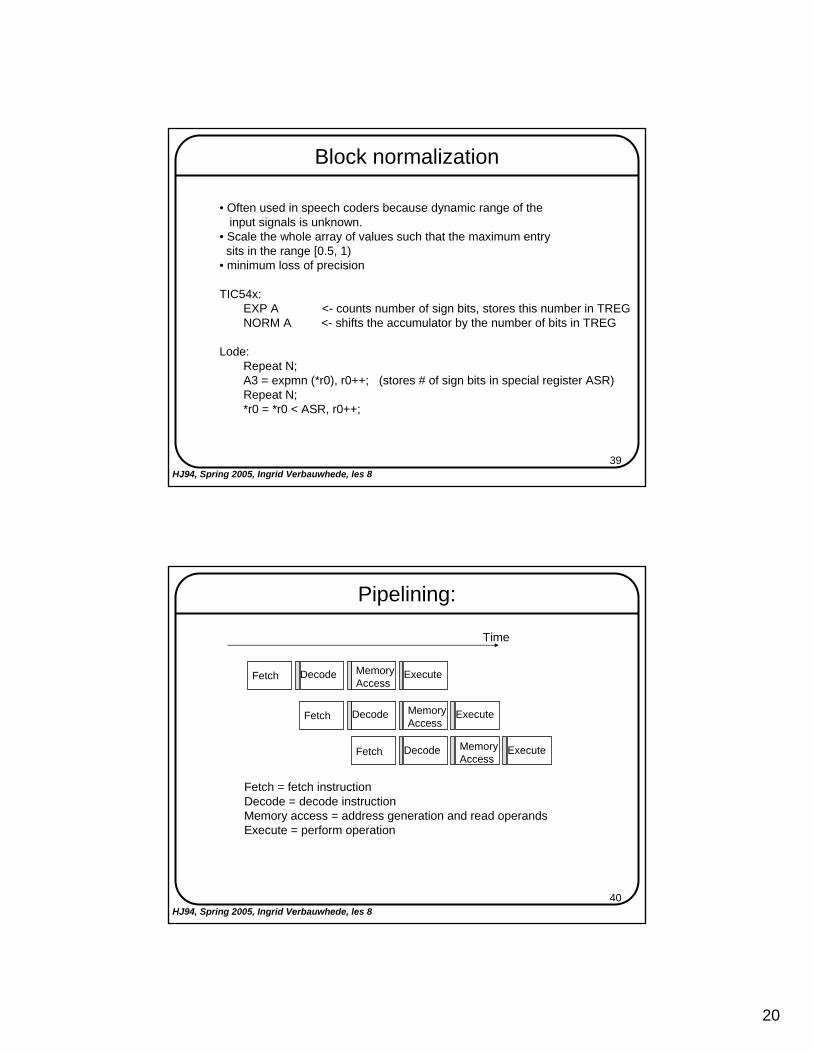
Overflow:
16 x 16 mpy
ALU32 bit
40 bitShifter/ saturate
Select 16 bit
40 bit
• Saturation logic combined with output shifter
• How to implement saturation?
38HJ94, Spring 2005, Ingrid Verbauwhede, les 8
Overflow:
16 x 16 mpy
ALU32 bit
40 bitShifter/ saturate
Select 16 bit
40 bit
• Input shifter: scaling, line up of the inputs= loss of precision if shift to much down.
input Shifter
20
39HJ94, Spring 2005, Ingrid Verbauwhede, les 8
Block normalization
• Often used in speech coders because dynamic range of theinput signals is unknown.
• Scale the whole array of values such that the maximum entrysits in the range [0.5, 1)
• minimum loss of precision
TIC54x: EXP A <- counts number of sign bits, stores this number in TREGNORM A <- shifts the accumulator by the number of bits in TREG
Lode:Repeat N;A3 = expmn (*r0), r0++; (stores # of sign bits in special register ASR)Repeat N;*r0 = *r0 < ASR, r0++;
40HJ94, Spring 2005, Ingrid Verbauwhede, les 8
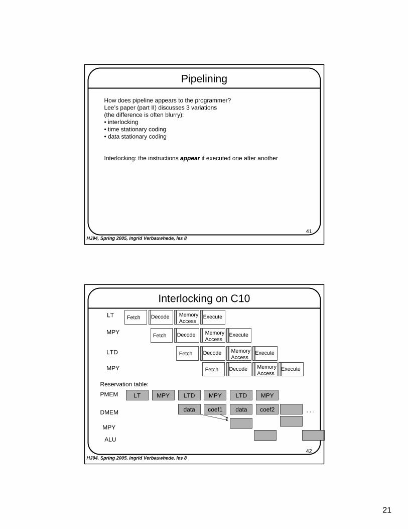
Pipelining:
ExecuteDecodeFetch MemoryAccess
ExecuteDecodeFetch MemoryAccess
ExecuteDecodeFetch MemoryAccess
Fetch = fetch instructionDecode = decode instructionMemory access = address generation and read operandsExecute = perform operation
Time
21
41HJ94, Spring 2005, Ingrid Verbauwhede, les 8
Pipelining
How does pipeline appears to the programmer?Lee’s paper (part II) discusses 3 variations(the difference is often blurry):• interlocking• time stationary coding• data stationary coding
Interlocking: the instructions appear if executed one after another
42HJ94, Spring 2005, Ingrid Verbauwhede, les 8
Interlocking on C10
LTPMEM MPY LTD
ExecuteDecodeFetch MemoryAccess
ExecuteDecodeFetch MemoryAccess
ExecuteDecodeFetch MemoryAccess
LT
MPY
LTD
ExecuteDecodeFetch MemoryAccess
MPY
MPY
DMEM data coef1 data coef2
ALU
MPY
Reservation table:
LTD MPY
. . .
22
43HJ94, Spring 2005, Ingrid Verbauwhede, les 8
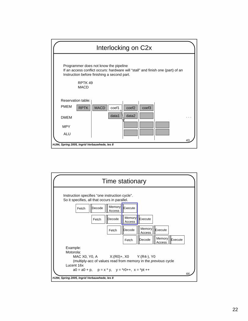
Interlocking on C2x
Programmer does not know the pipelineIf an access conflict occurs: hardware will “stall” and finish one (part) of anInstruction before finishing a second part.
RPTKPMEM MACD coef1 coef2
DMEM data1 data2
ALU
MPY
Reservation table:
. . .
RPTK 49MACD
coef3
44HJ94, Spring 2005, Ingrid Verbauwhede, les 8
Time stationary
Instruction specifies “one instruction cycle”.So it specifies, all that occurs in parallel.
ExecuteDecodeFetch MemoryAccess
ExecuteDecodeFetch MemoryAccess
ExecuteDecodeFetch MemoryAccess
ExecuteDecodeFetch MemoryAccess
Example:Motorola:
MAC X0, Y0, A X:(R0)+, X0 Y:(R4-), Y0(multiply-acc of values read from memory in the previous cycle
Lucent 16xa0 = a0 + p, p = x * y, y = *r0++, x = *pt ++
23
45HJ94, Spring 2005, Ingrid Verbauwhede, les 8
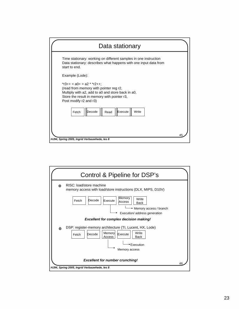
Data stationary
Time stationary: working on different samples in one instructionData stationary: describes what happens with one input data fromstart to end.
Example (Lode):
*r3++ = a0+ = a2 * *r2++;(read from memory with pointer reg r2,Multiply with a2, add to a0 and store back in a0,Store the result in memory with pointer r3,Post modify r2 and r3)
ExecuteDecodeFetch Read Write
46HJ94, Spring 2005, Ingrid Verbauwhede, les 8
Control & Pipeline for DSP’sRISC: load/store machinememory access with load/store instructions (DLX, MIPS, D10V)
MemoryAccessDecodeFetch Execute Write
Back
Memory access / branchExecution/ address generation
Excellent for complex decision making!
Memory accessExecution
DSP: register-memory architecture (TI, Lucent, HX, Lode)
Excellent for number crunching!
ExecuteDecodeFetch MemoryAccess
WriteBack
24
47HJ94, Spring 2005, Ingrid Verbauwhede, les 8
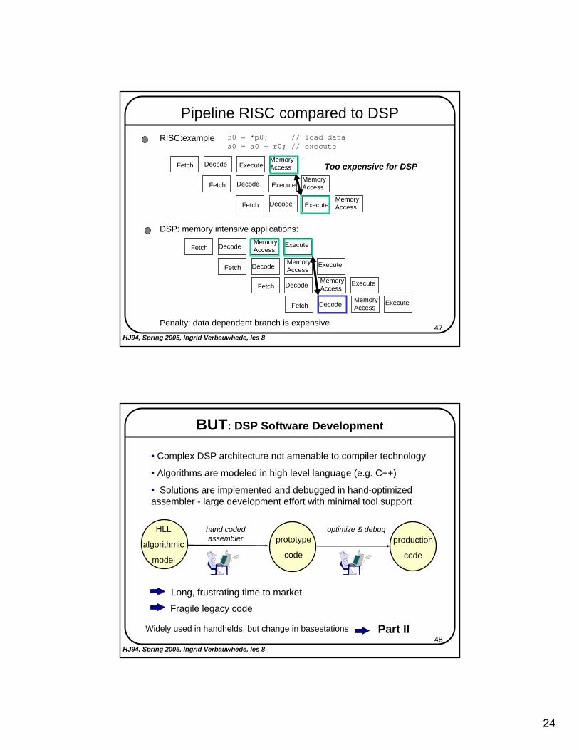
Pipeline RISC compared to DSPRISC:example
DSP: memory intensive applications:
r0 = *p0; // load dataa0 = a0 + r0; // execute
MemoryAccessDecodeFetch Execute
MemoryAccessDecodeFetch Execute
MemoryAccessDecodeFetch Execute
Too expensive for DSP
ExecuteDecodeFetchMemoryAccess
ExecuteDecodeFetchMemoryAccess
ExecuteDecodeFetchMemoryAccess
ExecuteDecodeFetchMemoryAccess
Penalty: data dependent branch is expensive
48HJ94, Spring 2005, Ingrid Verbauwhede, les 8
BUT: DSP Software Development
• Complex DSP architecture not amenable to compiler technology
• Algorithms are modeled in high level language (e.g. C++)
• Solutions are implemented and debugged in hand-optimized assembler - large development effort with minimal tool support
HLL
algorithmic
model
prototype
code
production
code
hand coded assembler
optimize & debug
Long, frustrating time to market
Fragile legacy code
Widely used in handhelds, but change in basestations Part II
25
49HJ94, Spring 2005, Ingrid Verbauwhede, les 8
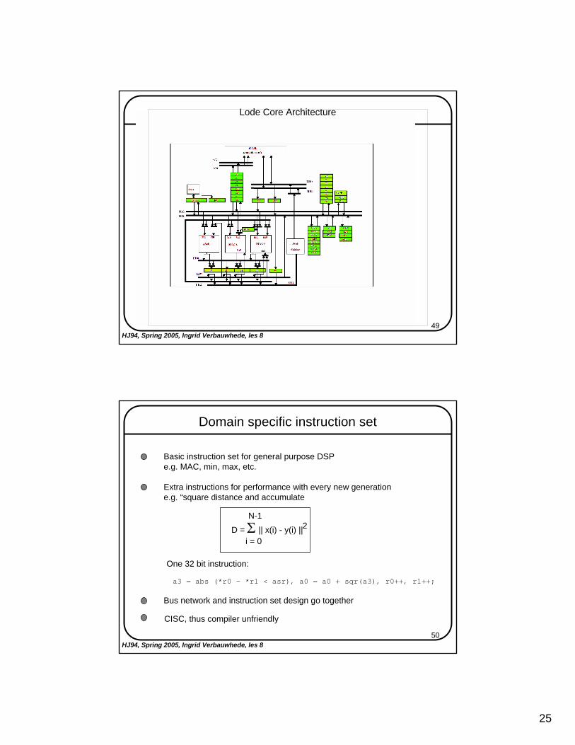
Lode Core Architecture
50HJ94, Spring 2005, Ingrid Verbauwhede, les 8
Domain specific instruction set
Basic instruction set for general purpose DSPe.g. MAC, min, max, etc.
Extra instructions for performance with every new generatione.g. “square distance and accumulate
D = Σ || x(i) - y(i) ||
N-1
i = 0
2
One 32 bit instruction:
a3 = abs (*r0 - *r1 < asr), a0 = a0 + sqr(a3), r0++, r1++;
Bus network and instruction set design go together
CISC, thus compiler unfriendly
26
51HJ94, Spring 2005, Ingrid Verbauwhede, les 8
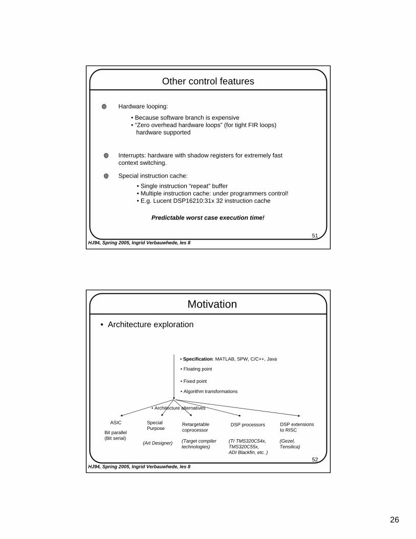
Other control features
Hardware looping:
• Because software branch is expensive• “Zero overhead hardware loops” (for tight FIR loops)
hardware supported
Interrupts: hardware with shadow registers for extremely fastcontext switching.
Special instruction cache:
• Single instruction “repeat” buffer• Multiple instruction cache: under programmers control!• E.g. Lucent DSP16210:31x 32 instruction cache
Predictable worst case execution time!
52HJ94, Spring 2005, Ingrid Verbauwhede, les 8
Motivation
• Architecture exploration
• Specification: MATLAB, SPW, C/C++, Java
• Floating point
• Fixed point
• Algorithm transformations
• Architecture alternatives
Bit parallel (Bit serial)
ASIC SpecialPurpose
(Art Designer)
Retargetablecoprocessor
(Target compilertechnologies)
DSP extensionsto RISC
DSP processors
(Gezel,Tensilica)
(TI TMS320C54x,TMS320C55x,ADI Blackfin, etc. )