Embed Size (px)
Citation preview

Chipsmall Limited consists of a professional team with an average of over 10 year of expertise in the distribution
of electronic components. Based in Hongkong, we have already established firm and mutual-benefit business
relationships with customers from,Europe,America and south Asia,supplying obsolete and hard-to-find components
to meet their specific needs.
With the principle of “Quality Parts,Customers Priority,Honest Operation,and Considerate Service”,our business
mainly focus on the distribution of electronic components. Line cards we deal with include
Microchip,ALPS,ROHM,Xilinx,Pulse,ON,Everlight and Freescale. Main products comprise
IC,Modules,Potentiometer,IC Socket,Relay,Connector.Our parts cover such applications as commercial,industrial,
and automotives areas.
We are looking forward to setting up business relationship with you and hope to provide you with the best service
and solution. Let us make a better world for our industry!
Contact usTel: +86-755-8981 8866 Fax: +86-755-8427 6832
Email & Skype: [email protected] Web: www.chipsmall.com
Address: A1208, Overseas Decoration Building, #122 Zhenhua RD., Futian, Shenzhen, China
2011 Microchip Technology Inc. DS70116J
dsPIC30F5011/5013
Data Sheet
High-Performance,
16-bit Digital Signal Controllers
DS70116J-page 2 2011 Microchip Technology Inc.
Information contained in this publication regarding device
applications and the like is provided only for your convenience
and may be superseded by updates. It is your responsibility to
ensure that your application meets with your specifications.
MICROCHIP MAKES NO REPRESENTATIONS OR
WARRANTIES OF ANY KIND WHETHER EXPRESS OR
IMPLIED, WRITTEN OR ORAL, STATUTORY OR
OTHERWISE, RELATED TO THE INFORMATION,
INCLUDING BUT NOT LIMITED TO ITS CONDITION,
QUALITY, PERFORMANCE, MERCHANTABILITY OR
FITNESS FOR PURPOSE. Microchip disclaims all liability
arising from this information and its use. Use of Microchip
devices in life support and/or safety applications is entirely at
the buyer’s risk, and the buyer agrees to defend, indemnify and
hold harmless Microchip from any and all damages, claims,
suits, or expenses resulting from such use. No licenses are
conveyed, implicitly or otherwise, under any Microchip
intellectual property rights.
Trademarks
The Microchip name and logo, the Microchip logo, dsPIC,
KEELOQ, KEELOQ logo, MPLAB, PIC, PICmicro, PICSTART,
PIC32 logo, rfPIC and UNI/O are registered trademarks of
Microchip Technology Incorporated in the U.S.A. and other
countries.
FilterLab, Hampshire, HI-TECH C, Linear Active Thermistor,
MXDEV, MXLAB, SEEVAL and The Embedded Control
Solutions Company are registered trademarks of Microchip
Technology Incorporated in the U.S.A.
Analog-for-the-Digital Age, Application Maestro, CodeGuard,
dsPICDEM, dsPICDEM.net, dsPICworks, dsSPEAK, ECAN,
ECONOMONITOR, FanSense, HI-TIDE, In-Circuit Serial
Programming, ICSP, Mindi, MiWi, MPASM, MPLAB Certified
logo, MPLIB, MPLINK, mTouch, Omniscient Code
Generation, PICC, PICC-18, PICDEM, PICDEM.net, PICkit,
PICtail, REAL ICE, rfLAB, Select Mode, Total Endurance,
TSHARC, UniWinDriver, WiperLock and ZENA are
trademarks of Microchip Technology Incorporated in the
U.S.A. and other countries.
SQTP is a service mark of Microchip Technology Incorporated
in the U.S.A.
All other trademarks mentioned herein are property of their
respective companies.
© 2011, Microchip Technology Incorporated, Printed in the
U.S.A., All Rights Reserved.
Printed on recycled paper.
ISBN: 978-1-60932-843-6
Note the following details of the code protection feature on Microchip devices:
� Microchip products meet the specification contained in their particular Microchip Data Sheet.
� Microchip believes that its family of products is one of the most secure families of its kind on the market today, when used in the
intended manner and under normal conditions.
� There are dishonest and possibly illegal methods used to breach the code protection feature. All of these methods, to our
knowledge, require using the Microchip products in a manner outside the operating specifications contained in Microchip’s Data
Sheets. Most likely, the person doing so is engaged in theft of intellectual property.
� Microchip is willing to work with the customer who is concerned about the integrity of their code.
� Neither Microchip nor any other semiconductor manufacturer can guarantee the security of their code. Code protection does not
mean that we are guaranteeing the product as “unbreakable.”
Code protection is constantly evolving. We at Microchip are committed to continuously improving the code protection features of our
products. Attempts to break Microchip’s code protection feature may be a violation of the Digital Millennium Copyright Act. If such acts
allow unauthorized access to your software or other copyrighted work, you may have a right to sue for relief under that Act.
Microchip received ISO/TS-16949:2002 certification for its worldwide headquarters, design and wafer fabrication facilities in Chandler and Tempe, Arizona; Gresham, Oregon and design centers in California and India. The Company’s quality system processes and procedures are for its PIC® MCUs and dsPIC® DSCs, KEELOQ® code hopping devices, Serial EEPROMs, microperipherals, nonvolatile memory and analog products. In addition, Microchip’s quality system for the design and manufacture of development systems is ISO 9001:2000 certified.
2011 Microchip Technology Inc. DS70116J-page 3
High-Performance Modified RISC CPU:
� Modified Harvard architecture
� C compiler optimized instruction set architecture
� Flexible addressing modes
� 83 base instructions
� 24-bit wide instructions, 16-bit wide data path
� 66 Kbytes on-chip Flash program space
� 4 Kbytes of on-chip data RAM
� 1 Kbyte of nonvolatile data EEPROM
� 16 x 16-bit working register array
� Up to 30 MIPS operation:
- DC to 40 MHz external clock input
- 4 MHz-10 MHz oscillator input with
PLL active (4x, 8x, 16x)
� Up to 41 interrupt sources:
- Eight user selectable priority levels
- Five external interrupt sources
- Four processor traps
DSP Features:
� Dual data fetch
� Modulo and Bit-Reversed modes
� Two 40-bit wide accumulators with optional
saturation logic
� 17-bit x 17-bit single cycle hardware fractional/
integer multiplier
� All DSP instructions are single cycle
- Multiply-Accumulate (MAC) operation
� Single cycle ±16 shift
Peripheral Features:
� High-current sink/source I/O pins: 25 mA/25 mA
� Five 16-bit timers/counters; optionally pair up
16-bit timers into 32-bit timer modules
� 16-bit Capture input functions
� 16-bit Compare/PWM output functions
� Data Converter Interface (DCI) supports common
audio codec protocols, including I2S and AC’97
� 3-wire SPI modules (supports four Frame modes)
� I2C™ module supports Multi-Master/Slave mode
and 7-bit/10-bit addressing
� Two addressable UART modules with FIFO
buffers
� Two CAN bus modules compliant with CAN 2.0B
standard
Analog Features:
� 12-bit Analog-to-Digital Converter (ADC) with:
- 200 ksps conversion rate
- Up to 16 input channels
- Conversion available during Sleep and Idle
� Programmable Low-Voltage Detection (PLVD)
� Programmable Brown-out Detection and Reset
generation
Special Microcontroller Features:
� Enhanced Flash program memory:
- 10,000 erase/write cycle (min.) for
industrial temperature range, 100K (typical)
� Data EEPROM memory:
- 100,000 erase/write cycle (min.) for
industrial temperature range, 1M (typical)
� Self-reprogrammable under software control
� Power-on Reset (POR), Power-up Timer (PWRT)
and Oscillator Start-up Timer (OST)
� Flexible Watchdog Timer (WDT) with on-chip
low- power RC oscillator for reliable operation
� Fail-Safe Clock Monitor operation:
- Detects clock failure and switches to on-chip
low-power RC oscillator
� Programmable code protection
� In-Circuit Serial Programming™ (ICSP™)
programming capability
� Selectable Power Management modes:
- Sleep, Idle and Alternate Clock modes
Note: This data sheet summarizes features of
this group of dsPIC30F devices and is not
intended to be a complete reference
source. For more information on the CPU,
peripherals, register descriptions and
general device functionality, refer to the
“dsPIC30F Family Reference Manual”
(DS70046). For more information on the
device instruction set and programming,
refer to the “16-bit MCU and DSC Pro-
grammer’s Reference Manual”
(DS70157).
dsPIC30F5011/5013
High-Performance, Digital Signal Controllers
dsPIC30F5011/5013
DS70116J-page 4 2011 Microchip Technology Inc.
CMOS Technology:
� Low-power, high-speed Flash technology
� Wide operating voltage range (2.5V to 5.5V)
� Industrial and Extended temperature ranges
� Low power consumption
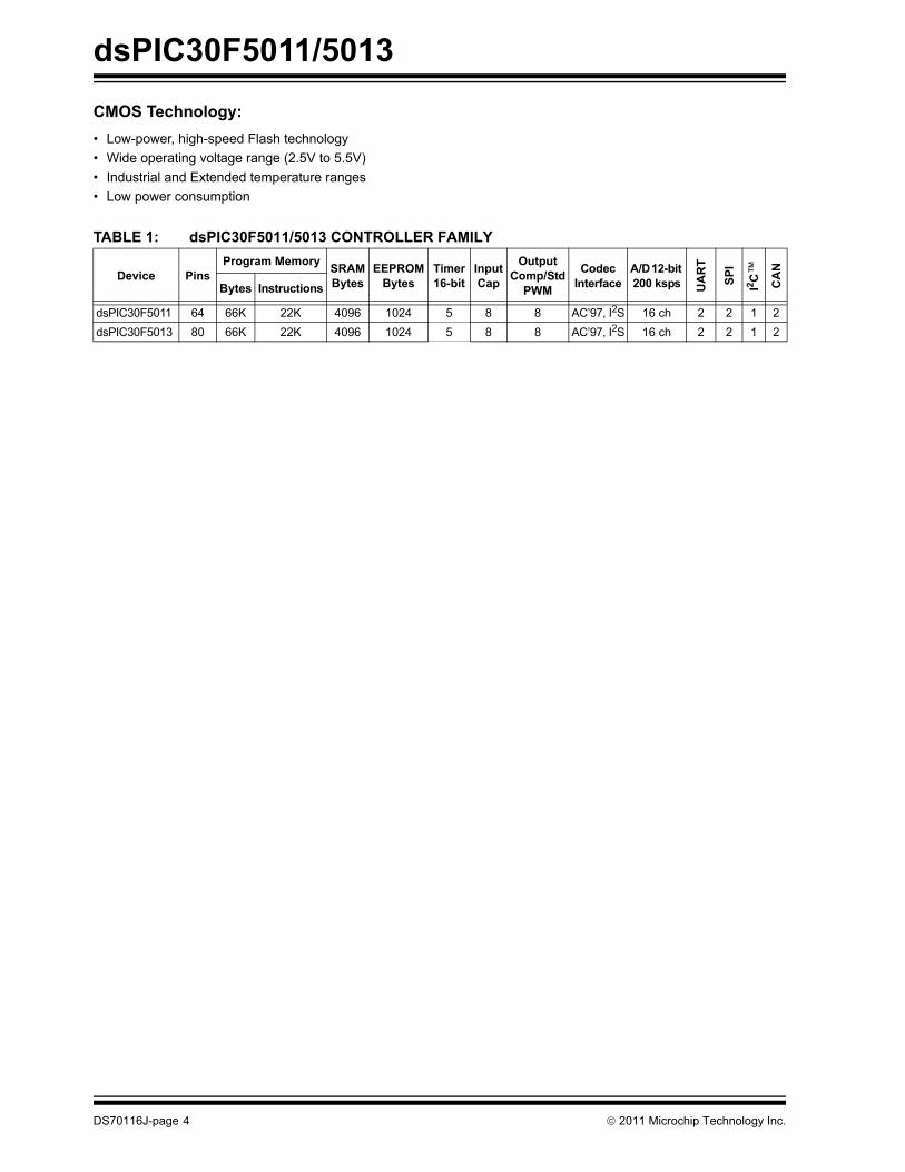
TABLE 1: dsPIC30F5011/5013 CONTROLLER FAMILY
Device Pins
Program MemorySRAM
Bytes
EEPROM
Bytes
Timer
16-bit
Input
Cap
Output
Comp/Std
PWM
Codec
Interface
A/D 12-bit
200 ksps UA
RT
SP
I
I2C
™
CA
N
Bytes Instructions
dsPIC30F5011 64 66K 22K 4096 1024 5 8 8 AC’97, I2S 16 ch 2 2 1 2
dsPIC30F5013 80 66K 22K 4096 1024 5 8 8 AC’97, I2S 16 ch 2 2 1 2
2011 Microchip Technology Inc. DS70116J-page 5
dsPIC30F5011/5013
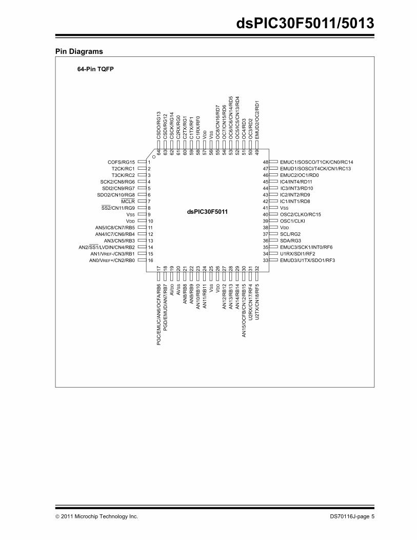
Pin Diagrams
1
2
3
4
5
6
7
8
9
10
11
12
13 36
35
34
333
2
31
30
29
28
27
26
64
63
62
61
60
59
58
57
56
14
15
16
17
18
19
20
21
22
23
24
25
EMUC1/SOSCO/T1CK/CN0/RC14
EMUD1/SOSCI/T4CK/CN1/RC13
EMUC2/OC1/RD0
IC4/INT4/RD11
IC2/INT2/RD9
IC1/INT1/RD8
VSS
OSC2/CLKO/RC15
OSC1/CLKI
VDD
SCL/RG2
EMUC3/SCK1/INT0/RF6
U1RX/SDI1/RF2
EMUD3/U1TX/SDO1/RF3
COFS/RG15
T2CK/RC1
T3CK/RC2
SCK2/CN8/RG6
SDI2/CN9/RG7
SDO2/CN10/RG8
MCLR
VSS
VDD
AN3/CN5/RB3
AN2/SS1/LVDIN/CN4/RB2
AN1/VREF-/CN3/RB1
AN0/VREF+/CN2/RB0
OC
8/C
N1
6/R
D7
CS
DO
/RG
13
CS
DI/
RG
12
CS
CK
/RG
14
VS
S
C2T
X/R
G1
C1T
X/R
F1
C2R
X/R
G0
EM
UD
2/O
C2
/RD
1
OC
3/R
D2
PG
C/E
MU
C/A
N6
/OC
FA
/RB
6
PG
D/E
MU
D/A
N7/R
B7
AV
DD
AV
SS
AN
8/R
B8
AN
9/R
B9
AN
10
/RB
10
AN
11
/RB
11
VS
S
VD
D
AN
12
/RB
12
AN
13
/RB
13
AN
14
/RB
14
AN
15
/OC
FB
/CN
12
/RB
15
U2
TX
/CN
18
/RF
5
U2
RX
/CN
17
/RF
4
SDA/RG3
43
42
41
40
39
38
37
44
48
47
46
50
49
51
54
53
52
55
45
SS2/CN11/RG9
AN5/IC8/CN7/RB5
AN4/IC7/CN6/RB4
IC3/INT3/RD10
VD
D
C1R
X/R
F0
OC
4/R
D3
OC
7/C
N1
5/R
D6
OC
6/I
C6
/CN
14
/RD
5
OC
5/I
C5
/CN
13
/RD
4
64-Pin TQFP
dsPIC30F5011
dsPIC30F5011/5013
DS70116J-page 6 2011 Microchip Technology Inc.
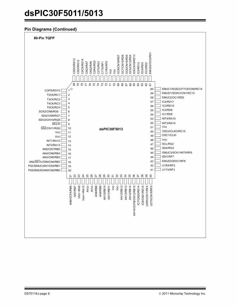
Pin Diagrams (Continued)
72
74
73
71
70
69
68
67
66
65
64
63
62
61
20
2
3
4
5
6
7
8
9
10
11
12
13
14
15
16
50
49
48
47
46
45
44
21
41
40
39
38
37
36
35
34
23
24
25
26
27
28
29
30
31
32
33
dsPIC30F5013
17
18
19
75
1
57
56
55
54
53
52
51
60
59
58
43
42
76
78
77
79
22
80
IC5/R
D1
2
OC
4/R
D3
OC
3/R
D2
EM
UD
2/O
C2
/RD
1
CS
CK
/RG
14
C2
RX
/RG
0
C2
TX
/RG
1
C1
TX
/RF
1
C1
RX
/RF
0
CS
DO
/RG
13
CS
DI/
RG
12
OC
8/C
N1
6/R
D7
OC
6/C
N1
4/R
D5
EMUC2/OC1/RD0
IC4/RD11
IC2/RD9
IC1/RD8
INT4/RA15
IC3/RD10
INT3/RA14
VSS
OSC1/CLKI
VDD
SCL/RG2
U1RX/RF2
U1TX/RF3
EMUC1/SOSCO/T1CK/CN0/RC14
EMUD1/SOSCI/CN1/RC13
VR
EF+
/RA
10
VR
EF-/
RA
9
AV
DD
AV
SS
AN
8/R
B8
AN
9/R
B9
AN
10
/RB
10
AN
11/R
B11
VD
D
U2
RX
/CN
17
/RF
4
IC8/C
N2
1/R
D1
5
U2
TX
/CN
18
/RF
5
AN
6/O
CF
A/R
B6
AN
7/R
B7
T3CK/RC2
T4CK/RC3
T5CK/RC4
SCK2/CN8/RG6
SDI2/CN9/RG7
SDO2/CN10/RG8
MCLR
SS2/CN11/RG9
AN4/CN6/RB4
AN3/CN5/RB3
AN2/SS1/LVDIN/CN4/RB2
PGC/EMUC/AN1/CN3/RB1
PGD/EMUD/AN0/CN2/RB0
VSS
VDD
COFS/RG15
T2CK/RC1
INT2/RA13
INT1/RA12
AN
12
/RB
12
AN
13
/RB
13
AN
14
/RB
14
AN
15
/OC
FB
/CN
12
/RB
15
VD
D
VS
S
OC
5/C
N1
3/R
D4
IC6/C
N1
9/R
D1
3
SDA/RG3
SDI1/RF7
EMUD3/SDO1/RF8
AN5/CN7/RB5
VS
S
OSC2/CLKO/RC15
OC
7/C
N1
5/R
D6
EMUC3/SCK1/INT0/RF6
IC7/C
N2
0/R
D1
4
80-Pin TQFP
CN
23
/RA
7
CN
22
/RA
6
2011 Microchip Technology Inc. DS70116J-page 7
dsPIC30F5011/5013
Table of Contents
1.0 Device Overview .......................................................................................................................................................................... 9
2.0 CPU Architecture Overview........................................................................................................................................................ 15
3.0 Memory Organization ................................................................................................................................................................. 23
4.0 Interrupts .................................................................................................................................................................................... 35
5.0 Address Generator Units............................................................................................................................................................ 41
6.0 Flash Program Memory.............................................................................................................................................................. 47
7.0 Data EEPROM Memory ............................................................................................................................................................. 53
8.0 I/O Ports ..................................................................................................................................................................................... 57
9.0 Timer1 Module ........................................................................................................................................................................... 63
10.0 Timer2/3 Module ........................................................................................................................................................................ 67
11.0 Timer4/5 Module ....................................................................................................................................................................... 73
12.0 Input Capture Module................................................................................................................................................................. 77
13.0 Output Compare Module ............................................................................................................................................................ 81
14.0 SPI™ Module ............................................................................................................................................................................. 87
15.0 I2C™ Module ............................................................................................................................................................................. 91
16.0 Universal Asynchronous Receiver Transmitter (UART) Module ................................................................................................ 99
17.0 CAN Module ............................................................................................................................................................................. 107
18.0 Data Converter Interface (DCI) Module.................................................................................................................................... 117
19.0 12-bit Analog-to-Digital Converter (ADC) Module .................................................................................................................... 127
20.0 System Integration ................................................................................................................................................................... 137
21.0 Instruction Set Summary .......................................................................................................................................................... 151
22.0 Development Support............................................................................................................................................................... 159
23.0 Electrical Characteristics .......................................................................................................................................................... 163
24.0 Packaging Information.............................................................................................................................................................. 203
Index .................................................................................................................................................................................................. 209
The Microchip Web Site..................................................................................................................................................................... 215
Customer Change Notification Service .............................................................................................................................................. 215
Customer Support .............................................................................................................................................................................. 215
Reader Response .............................................................................................................................................................................. 216
Product Identification System ............................................................................................................................................................ 217
TO OUR VALUED CUSTOMERS
It is our intention to provide our valued customers with the best documentation possible to ensure successful use of your Microchip
products. To this end, we will continue to improve our publications to better suit your needs. Our publications will be refined and
enhanced as new volumes and updates are introduced.
If you have any questions or comments regarding this publication, please contact the Marketing Communications Department via
E-mail at [email protected] or fax the Reader Response Form in the back of this data sheet to (480) 792-4150. We
welcome your feedback.
Most Current Data Sheet
To obtain the most up-to-date version of this data sheet, please register at our Worldwide Web site at:
http://www.microchip.com
You can determine the version of a data sheet by examining its literature number found on the bottom outside corner of any page.The last character of the literature number is the version number, (e.g., DS30000A is version A of document DS30000).
Errata
An errata sheet, describing minor operational differences from the data sheet and recommended workarounds, may exist for currentdevices. As device/documentation issues become known to us, we will publish an errata sheet. The errata will specify the revisionof silicon and revision of document to which it applies.
To determine if an errata sheet exists for a particular device, please check with one of the following:
� Microchip’s Worldwide Web site; http://www.microchip.com
� Your local Microchip sales office (see last page)
When contacting a sales office, please specify which device, revision of silicon and data sheet (include literature number) you areusing.
Customer Notification System
Register on our web site at www.microchip.com to receive the most current information on all of our products.
dsPIC30F5011/5013
DS70116J-page 8 2011 Microchip Technology Inc.
NOTES:
2011 Microchip Technology Inc. DS70116J-page 9
dsPIC30F5011/5013
1.0 DEVICE OVERVIEW
This document contains specific information for the
dsPIC30F5011/5013 Digital Signal Controller (DSC)
devices. The dsPIC30F5011/5013 devices contain
extensive Digital Signal Processor (DSP) functionality
within a high-performance 16-bit microcontroller (MCU)
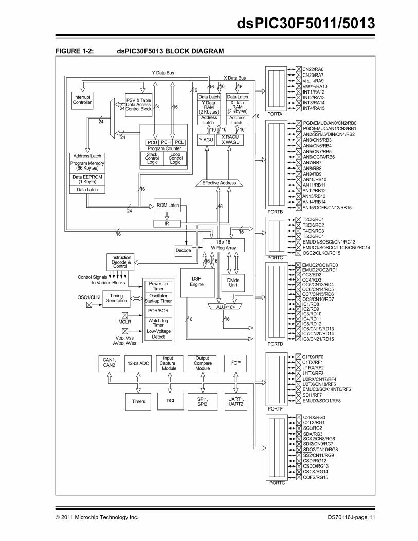
architecture. Figure 1-1 and Figure 1-2 show device
block diagrams for dsPIC30F5011 and dsPIC30F5013,
respectively.
Note: This data sheet summarizes features of
this group of dsPIC30F devices and is not
intended to be a complete reference
source. For more information on the CPU,
peripherals, register descriptions and
general device functionality, refer to the
“dsPIC30F Family Reference Manual”
(DS70046). For more information on the
device instruction set and programming,
refer to the “16-bit MCU and DSC
Programmer’s Reference Manual”
(DS70157).
dsPIC30F5011/5013
DS70116J-page 10 2011 Microchip Technology Inc.
FIGURE 1-1: dsPIC30F5011 BLOCK DIAGRAM
AN8/RB8AN9/RB9AN10/RB10
AN11/RB11
Power-upTimer
OscillatorStart-up Timer
POR/BOR
WatchdogTimer
InstructionDecode &Control
OSC1/CLKI
MCLR
VDD, VSS
AN4/IC7/CN6/RB4
AN12/RB12
AN13/RB13
AN14/RB14AN15/OCFB/CN12/RB15
Low-VoltageDetect
UART1,
CAN2
TimingGeneration
CAN1,
AN5/IC8/CN7/RB5
16
PCH PCL
Program Counter
ALU<16>
16
24
24
24
24
X Data Bus
IR
I2C™
DCI
PGC/EMUC/AN6/OCFA/RB6
PGD/EMUD/AN7/RB7
PCU
12-bit ADC
Timers
SCK2/CN8/RG6SDI2/CN9/RG7SDO2/CN10/RG8
SS2/CN11/RG9
U2TX/CN18/RF5EMUC3/SCK1/INT0/RF6
Input Capture Module
OutputCompareModule
EMUC1/SOSCO/T1CK/CN0/RC14EMUD1/SOSCI/T4CK/CN1/RC13
T2CK/RC1
PORTB
C1RX/RF0C1TX/RF1U1RX/SDI1/RF2EMUD3/U1TX/SDO1/RF3
C2RX/RG0C2TX/RG1SCL/RG2
SDA/RG3
PORTG
PORTD
16
16 16
16 x 16
W Reg Array
Divide Unit Engine
DSP
Decode
ROM Latch
16
Y Data Bus
Effective Address
X RAGUX WAGU
Y AGU
AN0/VREF+/CN2/RB0AN1/VREF-/CN3/RB1AN2/SS1/LVDIN/CN4/RB2
AN3/CN5/RB3
OSC2/CLKO/RC15
U2RX/CN17/RF4
AVDD, AVSS
UART2SPI2
16
16
16
16
16
PORTC
PORTF
16
16
16
16
8
InterruptController PSV & Table
Data AccessControl Block
StackControl Logic
LoopControlLogic
Data LatchData Latch
Y Data
(2 Kbytes)RAM
X Data
(2 Kbytes)RAM
AddressLatch
AddressLatch
Control Signals to Various Blocks
EMUC2/OC1/RD0EMUD2/OC2/RD1OC3/RD2OC4/RD3OC5/IC5/CN13/RD4OC6/IC6/CN14/RD5OC7/CN15/RD6OC8/CN16/RD7IC1/INT1/RD8IC2/INT2/RD9IC3/INT3/RD10IC4/INT4/RD11
16
CSDI/RG12CSDO/RG13CSCK/RG14
COFS/RG15
T3CK/RC2
SPI1,
Address Latch
Program
(66 Kbytes)
Data Latch
Data EEPROM(1 Kbyte)
16
Memory
2011 Microchip Technology Inc. DS70116J-page 11
dsPIC30F5011/5013
FIGURE 1-2: dsPIC30F5013 BLOCK DIAGRAM
AN8/RB8AN9/RB9AN10/RB10
AN11/RB11
Power-upTimer
OscillatorStart-up Timer
POR/BOR
WatchdogTimer
InstructionDecode &Control
OSC1/CLKI
MCLR
VDD, VSS
AN4/CN6/RB4
AN12/RB12
AN13/RB13
AN14/RB14AN15/OCFB/CN12/RB15
Low-VoltageDetect
UART1,
INT4/RA15INT3/RA14
VREF+/RA10
VREF-/RA9
CAN2
TimingGeneration
CAN1,
AN5/CN7/RB5
16
PCH PCL
Program Counter
ALU<16>
16
24
24
24
24
X Data Bus
IR
I2C™
DCI
AN6/OCFA/RB6
AN7/RB7
PCU
12-bit ADC
Timers
SCK2/CN8/RG6SDI2/CN9/RG7SDO2/CN10/RG8
SS2/CN11/RG9
U2TX/CN18/RF5EMUC3/SCK1/INT0/RF6SDI1/RF7
EMUD3/SDO1/RF8
Input Capture Module
OutputCompareModule
EMUC1/SOSCO/T1CK/CN0/RC14EMUD1/SOSCI/CN1/RC13
T4CK/RC3
T2CK/RC1
PORTB
C1RX/RF0C1TX/RF1U1RX/RF2U1TX/RF3
C2RX/RG0C2TX/RG1SCL/RG2
SDA/RG3
PORTG
PORTD
16
16 16
16 x 16
W Reg Array
Divide Unit Engine
DSP
Decode
ROM Latch
16
Y Data Bus
Effective Address
X RAGUX WAGU
Y AGU
PGD/EMUD/AN0/CN2/RB0PGC/EMUC/AN1/CN3/RB1AN2/SS1/LVDIN/CN4/RB2
AN3/CN5/RB3
OSC2/CLKO/RC15
U2RX/CN17/RF4
AVDD, AVSS
UART2SPI2
16
16
16
16
16 PORTA
PORTC
PORTF
16
16
16
16
8
InterruptController PSV & Table
Data AccessControl Block
StackControl Logic
LoopControlLogic
Data LatchData Latch
Y Data
(2 Kbytes)RAM
X Data
(2 Kbytes)RAM
AddressLatch
AddressLatch
Control Signals to Various Blocks
EMUC2/OC1/RD0EMUD2/OC2/RD1OC3/RD2OC4/RD3OC5/CN13/RD4OC6/CN14/RD5OC7/CN15/RD6OC8/CN16/RD7IC1/RD8IC2/RD9IC3/RD10IC4/RD11IC5/RD12IC6/CN19/RD13IC7/CN20/RD14IC8/CN21/RD15
16
CSDI/RG12CSDO/RG13CSCK/RG14
COFS/RG15
T3CK/RC2
SPI1,
INT1/RA12INT2/RA13
CN23/RA7
CN22/RA6
T5CK/RC4
Address Latch
Program Memory(66 Kbytes)
Data Latch
Data EEPROM(1 Kbyte)
16
dsPIC30F5011/5013
DS70116J-page 12 2011 Microchip Technology Inc.
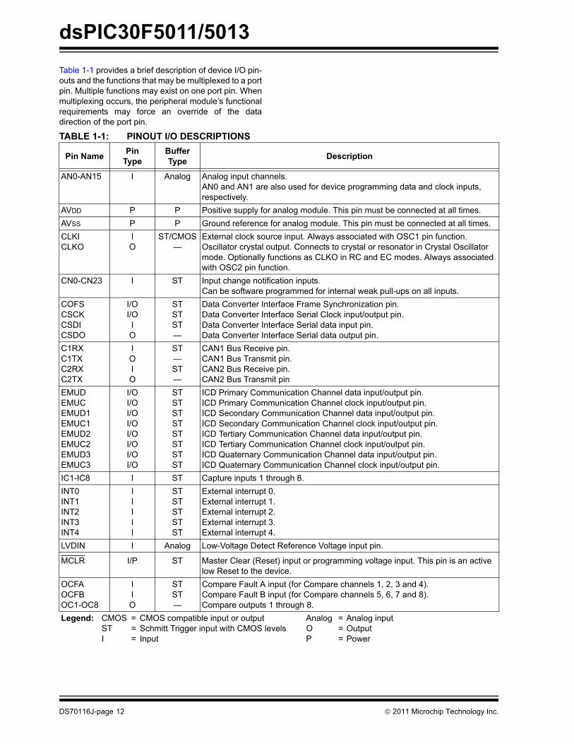
Table 1-1 provides a brief description of device I/O pin-
outs and the functions that may be multiplexed to a port
pin. Multiple functions may exist on one port pin. When
multiplexing occurs, the peripheral module’s functional
requirements may force an override of the data
direction of the port pin.
TABLE 1-1: PINOUT I/O DESCRIPTIONS
Pin NamePin
Type
Buffer
TypeDescription
AN0-AN15 I Analog Analog input channels.
AN0 and AN1 are also used for device programming data and clock inputs,
respectively.
AVDD P P Positive supply for analog module. This pin must be connected at all times.
AVSS P P Ground reference for analog module. This pin must be connected at all times.
CLKI
CLKO
I
O
ST/CMOS
—
External clock source input. Always associated with OSC1 pin function.
Oscillator crystal output. Connects to crystal or resonator in Crystal Oscillator
mode. Optionally functions as CLKO in RC and EC modes. Always associated
with OSC2 pin function.
CN0-CN23 I ST Input change notification inputs.
Can be software programmed for internal weak pull-ups on all inputs.
COFS
CSCK
CSDI
CSDO
I/O
I/O
I
O
ST
ST
ST
—
Data Converter Interface Frame Synchronization pin.
Data Converter Interface Serial Clock input/output pin.
Data Converter Interface Serial data input pin.
Data Converter Interface Serial data output pin.
C1RX
C1TX
C2RX
C2TX
I
O
I
O
ST
—
ST
—
CAN1 Bus Receive pin.
CAN1 Bus Transmit pin.
CAN2 Bus Receive pin.
CAN2 Bus Transmit pin
EMUD
EMUC
EMUD1
EMUC1
EMUD2
EMUC2
EMUD3
EMUC3
I/O
I/O
I/O
I/O
I/O
I/O
I/O
I/O
ST
ST
ST
ST
ST
ST
ST
ST
ICD Primary Communication Channel data input/output pin.
ICD Primary Communication Channel clock input/output pin.
ICD Secondary Communication Channel data input/output pin.
ICD Secondary Communication Channel clock input/output pin.
ICD Tertiary Communication Channel data input/output pin.
ICD Tertiary Communication Channel clock input/output pin.
ICD Quaternary Communication Channel data input/output pin.
ICD Quaternary Communication Channel clock input/output pin.
IC1-IC8 I ST Capture inputs 1 through 8.
INT0
INT1
INT2
INT3
INT4
I
I
I
I
I
ST
ST
ST
ST
ST
External interrupt 0.
External interrupt 1.
External interrupt 2.
External interrupt 3.
External interrupt 4.
LVDIN I Analog Low-Voltage Detect Reference Voltage input pin.
MCLR I/P ST Master Clear (Reset) input or programming voltage input. This pin is an active
low Reset to the device.
OCFA
OCFB
OC1-OC8
I
I
O
ST
ST
—
Compare Fault A input (for Compare channels 1, 2, 3 and 4).
Compare Fault B input (for Compare channels 5, 6, 7 and 8).
Compare outputs 1 through 8.
Legend: CMOS = CMOS compatible input or output Analog = Analog input
ST = Schmitt Trigger input with CMOS levels O = Output
I = Input P = Power
2011 Microchip Technology Inc. DS70116J-page 13
dsPIC30F5011/5013
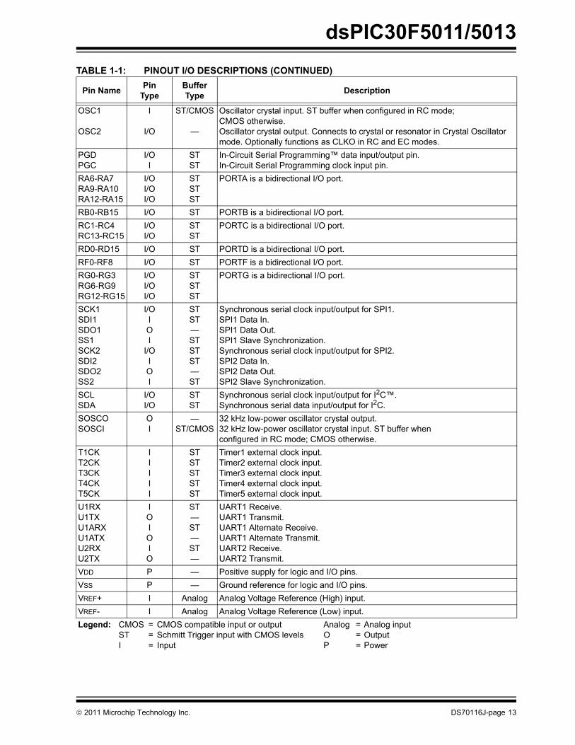
OSC1
OSC2
I
I/O
ST/CMOS
—
Oscillator crystal input. ST buffer when configured in RC mode;
CMOS otherwise.
Oscillator crystal output. Connects to crystal or resonator in Crystal Oscillator
mode. Optionally functions as CLKO in RC and EC modes.
PGD
PGC
I/O
I
ST
ST
In-Circuit Serial Programming™ data input/output pin.
In-Circuit Serial Programming clock input pin.
RA6-RA7
RA9-RA10
RA12-RA15
I/O
I/O
I/O
ST
ST
ST
PORTA is a bidirectional I/O port.
RB0-RB15 I/O ST PORTB is a bidirectional I/O port.
RC1-RC4
RC13-RC15
I/O
I/O
ST
ST
PORTC is a bidirectional I/O port.
RD0-RD15 I/O ST PORTD is a bidirectional I/O port.
RF0-RF8 I/O ST PORTF is a bidirectional I/O port.
RG0-RG3
RG6-RG9
RG12-RG15
I/O
I/O
I/O
ST
ST
ST
PORTG is a bidirectional I/O port.
SCK1
SDI1
SDO1
SS1
SCK2
SDI2
SDO2
SS2
I/O
I
O
I
I/O
I
O
I
ST
ST
—
ST
ST
ST
—
ST
Synchronous serial clock input/output for SPI1.
SPI1 Data In.
SPI1 Data Out.
SPI1 Slave Synchronization.
Synchronous serial clock input/output for SPI2.
SPI2 Data In.
SPI2 Data Out.
SPI2 Slave Synchronization.
SCL
SDA
I/O
I/O
ST
ST
Synchronous serial clock input/output for I2C™.
Synchronous serial data input/output for I2C.
SOSCO
SOSCI
O
I
—
ST/CMOS
32 kHz low-power oscillator crystal output.
32 kHz low-power oscillator crystal input. ST buffer when
configured in RC mode; CMOS otherwise.
T1CK
T2CK
T3CK
T4CK
T5CK
I
I
I
I
I
ST
ST
ST
ST
ST
Timer1 external clock input.
Timer2 external clock input.
Timer3 external clock input.
Timer4 external clock input.
Timer5 external clock input.
U1RX
U1TX
U1ARX
U1ATX
U2RX
U2TX
I
O
I
O
I
O
ST
—
ST
—
ST
—
UART1 Receive.
UART1 Transmit.
UART1 Alternate Receive.
UART1 Alternate Transmit.
UART2 Receive.
UART2 Transmit.
VDD P — Positive supply for logic and I/O pins.
VSS P — Ground reference for logic and I/O pins.
VREF+ I Analog Analog Voltage Reference (High) input.
VREF- I Analog Analog Voltage Reference (Low) input.
TABLE 1-1: PINOUT I/O DESCRIPTIONS (CONTINUED)
Pin NamePin
Type
Buffer
TypeDescription
Legend: CMOS = CMOS compatible input or output Analog = Analog input
ST = Schmitt Trigger input with CMOS levels O = Output
I = Input P = Power

dsPIC30F5011/5013
DS70116J-page 14 2011 Microchip Technology Inc.
NOTES:
2011 Microchip Technology Inc. DS70116J-page 15
dsPIC30F5011/5013
2.0 CPU ARCHITECTURE OVERVIEW
2.1 Core Overview
This section contains a brief overview of the CPU
architecture of the dsPIC30F. For additional hard-
ware and programming information, please refer to
the “dsPIC30F Family Reference Manual” (DS70046)
and the “16-bit MCU and DSC Programmer’s
Reference Manual” (DS70157), respectively.
The core has a 24-bit instruction word. The Program
Counter (PC) is 23 bits wide with the Least Significant
bit (LSb) always clear (refer to Section 3.1 “Program
Address Space”), and the Most Significant bit (MSb)
is ignored during normal program execution, except for
certain specialized instructions. Thus, the PC can
address up to 4M instruction words of user program
space. An instruction prefetch mechanism is used to
help maintain throughput. Program loop constructs,
free from loop count management overhead, are sup-
ported using the DO and REPEAT instructions, both of
which are interruptible at any point.
The working register array consists of 16 x 16-bit regis-
ters, each of which can act as data, address or offset
registers. One working register (W15) operates as a
software Stack Pointer for interrupts and calls.
The data space is 64 Kbytes (32K words) and is split
into two blocks, referred to as X and Y data memory.
Each block has its own independent Address Genera-
tion Unit (AGU). Most instructions operate solely
through the X memory, AGU, which provides the
appearance of a single unified data space. The
Multiply-Accumulate (MAC) class of dual source DSP
instructions operate through both the X and Y AGUs,
splitting the data address space into two parts (see
Section 3.2 “Data Address Space”). The X and Y
data space boundary is device specific and cannot be
altered by the user. Each data word consists of 2 bytes,
and most instructions can address data either as words
or bytes.
There are two methods of accessing data stored in
program memory:
� The upper 32 Kbytes of data space memory can
be mapped into the lower half (user space) of pro-
gram space at any 16K program word boundary,
defined by the 8-bit Program Space Visibility
Page (PSVPAG) register. This lets any instruction
access program space as if it were data space,
with a limitation that the access requires an addi-
tional cycle. Moreover, only the lower 16 bits of
each instruction word can be accessed using this
method.
� Linear indirect access of 32K word pages within
program space is also possible using any working
register, via table read and write instructions.
Table read and write instructions can be used to
access all 24 bits of an instruction word.
Overhead-free circular buffers (modulo addressing) are
supported in both X and Y address spaces. This is
primarily intended to remove the loop overhead for
DSP algorithms.
The X AGU also supports bit-reversed addressing on
destination effective addresses to greatly simplify input
or output data reordering for radix-2 FFT algorithms.
Refer to Section 5.0 “Address Generator Units” for
details on modulo and bit-reversed addressing.
The core supports Inherent (no operand), Relative,
Literal, Memory Direct, Register Direct, Register
Indirect, Register Offset and Literal Offset Addressing
modes. Instructions are associated with predefined
Addressing modes, depending upon their functional
requirements.
For most instructions, the core is capable of executing
a data (or program data) memory read, a working reg-
ister (data) read, a data memory write and a program
(instruction) memory read per instruction cycle. As a
result, 3-operand instructions are supported, allowing
C = A + B operations to be executed in a single cycle.
A DSP engine has been included to significantly
enhance the core arithmetic capability and throughput.
It features a high-speed 17-bit by 17-bit multiplier, a
40-bit ALU, two 40-bit saturating accumulators and a
40-bit bidirectional barrel shifter. Data in the accumula-
tor or any working register can be shifted up to 15 bits
right, or 16 bits left in a single cycle. The DSP instruc-
tions operate seamlessly with all other instructions and
have been designed for optimal real-time performance.
The MAC class of instructions can concurrently fetch
two data operands from memory while multiplying two
W registers. To enable this concurrent fetching of data
operands, the data space has been split for these
instructions and linear for all others. This has been
achieved in a transparent and flexible manner, by ded-
icating certain working registers to each address space
for the MAC class of instructions.
Note: This data sheet summarizes features of
this group of dsPIC30F devices and is not
intended to be a complete reference
source. For more information on the CPU,
peripherals, register descriptions and
general device functionality, refer to the
“dsPIC30F Family Reference Manual”
(DS70046). For more information on the
device instruction set and programming,
refer to the “16-bit MCU and DSC
Programmer’s Reference Manual”
(DS70157).
dsPIC30F5011/5013
DS70116J-page 16 2011 Microchip Technology Inc.
The core does not support a multi-stage instruction
pipeline. However, a single stage instruction prefetch
mechanism is used, which accesses and partially
decodes instructions a cycle ahead of execution, in
order to maximize available execution time. Most
instructions execute in a single cycle with certain
exceptions.
The core features a vectored exception processing
structure for traps and interrupts, with 62 independent
vectors. The exceptions consist of up to 8 traps (of
which 4 are reserved) and 54 interrupts. Each interrupt
is prioritized based on a user assigned priority between
1 and 7 (1 being the lowest priority and 7 being the
highest), in conjunction with a predetermined ‘natural
order’. Traps have fixed priorities ranging from 8 to 15.
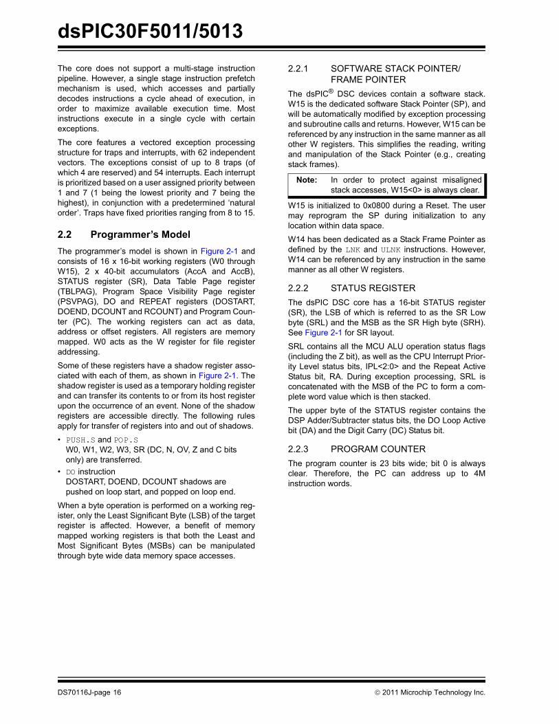
2.2 Programmer’s Model
The programmer’s model is shown in Figure 2-1 and
consists of 16 x 16-bit working registers (W0 through
W15), 2 x 40-bit accumulators (AccA and AccB),
STATUS register (SR), Data Table Page register
(TBLPAG), Program Space Visibility Page register
(PSVPAG), DO and REPEAT registers (DOSTART,
DOEND, DCOUNT and RCOUNT) and Program Coun-
ter (PC). The working registers can act as data,
address or offset registers. All registers are memory
mapped. W0 acts as the W register for file register
addressing.
Some of these registers have a shadow register asso-
ciated with each of them, as shown in Figure 2-1. The
shadow register is used as a temporary holding register
and can transfer its contents to or from its host register
upon the occurrence of an event. None of the shadow
registers are accessible directly. The following rules
apply for transfer of registers into and out of shadows.
� PUSH.S and POP.S
W0, W1, W2, W3, SR (DC, N, OV, Z and C bits
only) are transferred.
� DO instruction
DOSTART, DOEND, DCOUNT shadows are
pushed on loop start, and popped on loop end.
When a byte operation is performed on a working reg-
ister, only the Least Significant Byte (LSB) of the target
register is affected. However, a benefit of memory
mapped working registers is that both the Least and
Most Significant Bytes (MSBs) can be manipulated
through byte wide data memory space accesses.
2.2.1 SOFTWARE STACK POINTER/
FRAME POINTER
The dsPIC® DSC devices contain a software stack.
W15 is the dedicated software Stack Pointer (SP), and
will be automatically modified by exception processing
and subroutine calls and returns. However, W15 can be
referenced by any instruction in the same manner as all
other W registers. This simplifies the reading, writing
and manipulation of the Stack Pointer (e.g., creating
stack frames).
W15 is initialized to 0x0800 during a Reset. The user
may reprogram the SP during initialization to any
location within data space.
W14 has been dedicated as a Stack Frame Pointer as
defined by the LNK and ULNK instructions. However,
W14 can be referenced by any instruction in the same
manner as all other W registers.
2.2.2 STATUS REGISTER
The dsPIC DSC core has a 16-bit STATUS register
(SR), the LSB of which is referred to as the SR Low
byte (SRL) and the MSB as the SR High byte (SRH).
See Figure 2-1 for SR layout.
SRL contains all the MCU ALU operation status flags
(including the Z bit), as well as the CPU Interrupt Prior-
ity Level status bits, IPL<2:0> and the Repeat Active
Status bit, RA. During exception processing, SRL is
concatenated with the MSB of the PC to form a com-
plete word value which is then stacked.
The upper byte of the STATUS register contains the
DSP Adder/Subtracter status bits, the DO Loop Active
bit (DA) and the Digit Carry (DC) Status bit.
2.2.3 PROGRAM COUNTER
The program counter is 23 bits wide; bit 0 is always
clear. Therefore, the PC can address up to 4M
instruction words.
Note: In order to protect against misaligned
stack accesses, W15<0> is always clear.
2011 Microchip Technology Inc. DS70116J-page 17
dsPIC30F5011/5013
FIGURE 2-1: PROGRAMMER’S MODEL
TABPAG
PC22 PC0
7 0
D0D15
Program Counter
Data Table Page Address
STATUS Register
Working Registers
DSP Operand
Registers
W1
W2
W3
W4
W5
W6
W7
W8
W9
W10
W11
W12/DSP Offset
W13/DSP Write Back
W14/Frame Pointer
W15/Stack Pointer
DSP Address
Registers
AD39 AD0AD31
DSP
Accumulators
AccA
AccB
PSVPAG
7 0
Program Space Visibility Page Address
Z
0
OA OB SA SB
RCOUNT
15 0
REPEAT Loop Counter
DCOUNT
15 0
DO Loop Counter
DOSTART
22 0
DO Loop Start Address
IPL2 IPL1
SPLIM Stack Pointer Limit Register
AD15
SRL
PUSH.S Shadow
DO Shadow
OAB SAB
15 0
Core Configuration Register
Legend
CORCON
DA DC RA N
TBLPAG
PSVPAG
IPL0 OV
W0/WREG
SRH
DO Loop End AddressDOEND
22
C
dsPIC30F5011/5013
DS70116J-page 18 2011 Microchip Technology Inc.
2.3 Divide Support
The dsPIC DSC devices feature a 16/16-bit signed
fractional divide operation, as well as 32/16-bit and 16/
16-bit signed and unsigned integer divide operations, in
the form of single instruction iterative divides. The
following instructions and data sizes are supported:
� DIVF - 16/16 signed fractional divide
� DIV.sd - 32/16 signed divide
� DIV.ud - 32/16 unsigned divide
� DIV.sw - 16/16 signed divide
� DIV.uw - 16/16 unsigned divide
The 16/16 divides are similar to the 32/16 (same number
of iterations), but the dividend is either zero-extended or
sign-extended during the first iteration.
The divide instructions must be executed within a
REPEAT loop. Any other form of execution (e.g., a
series of discrete divide instructions) will not function
correctly because the instruction flow depends on
RCOUNT. The divide instruction does not automatically
set up the RCOUNT value and it must, therefore, be
explicitly and correctly specified in the REPEAT instruc-
tion as shown in Table 2-2 (REPEAT will execute the tar-
get instruction {operand value+1} times). The REPEAT
loop count must be setup for 18 iterations of the DIV/
DIVF instruction. Thus, a complete divide operation
requires 19 cycles.
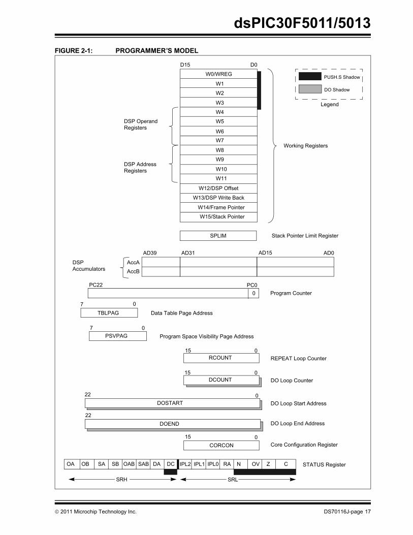
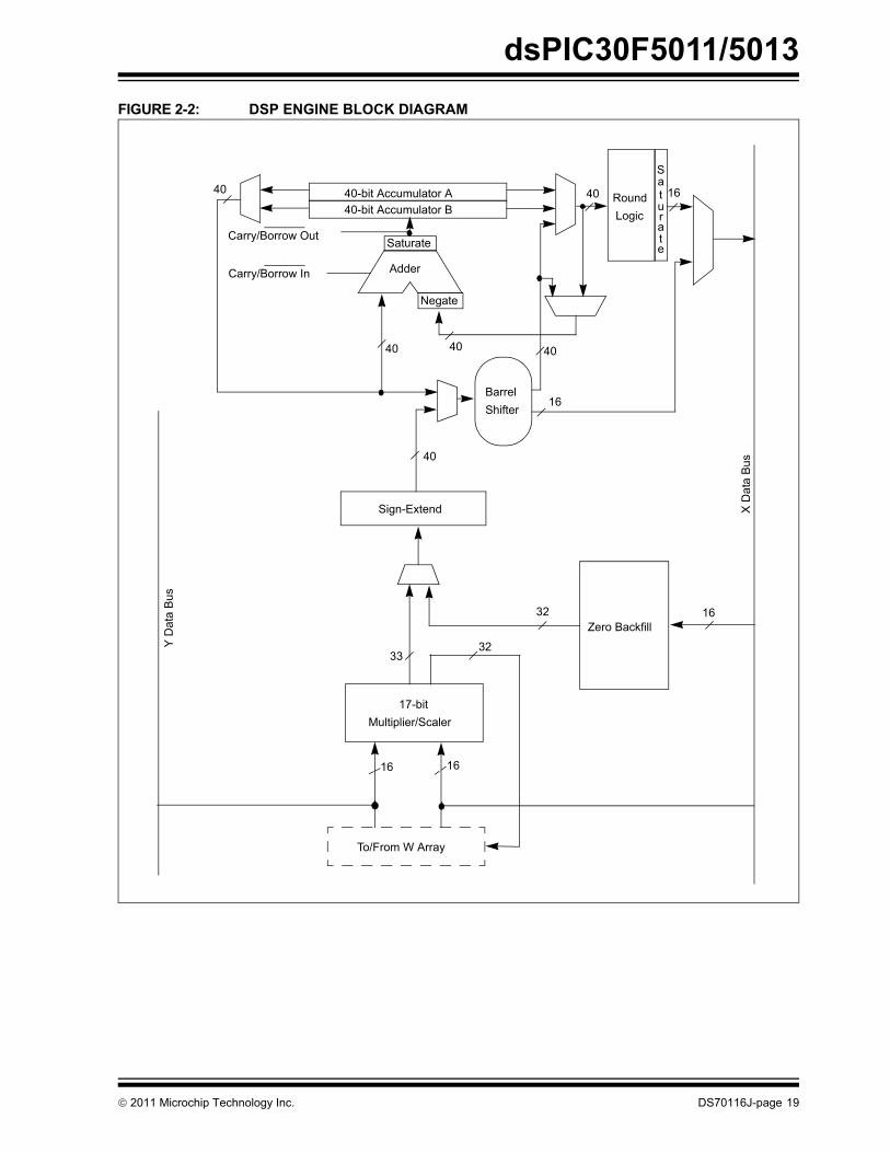
2.4 DSP Engine
The DSP engine consists of a high-speed 17-bit x17-bit multiplier, a barrel shifter and a 40-bit adder/subtracter (with two target accumulators, round andsaturation logic).
The DSP engine also has the capability to performinherent accumulator-to-accumulator operations,which require no additional data. These instructions areADD, SUB and NEG.
The dsPIC30F is a single-cycle instruction flow archi-tecture; therefore, concurrent operation of the DSPengine with MCU instruction flow is not possible.However, some MCU ALU and DSP engine resourcesmay be used concurrently by the same instruction (e.g.,ED, EDAC).
The DSP engine has various options selected throughvarious bits in the CPU Core Configuration register(CORCON), as listed below:
� Fractional or integer DSP multiply (IF)
� Signed or unsigned DSP multiply (US)
� Conventional or convergent rounding (RND)
� Automatic saturation on/off for AccA (SATA)
� Automatic saturation on/off for AccB (SATB)
� Automatic saturation on/off for writes to data
memory (SATDW)
� Accumulator Saturation mode selection
(ACCSAT)
A block diagram of the DSP engine is shown in
Figure 2-2.
TABLE 2-2: DIVIDE INSTRUCTIONS
Note: The divide flow is interruptible. However,
the user needs to save the context as
appropriate.Note: For CORCON layout, see Table 3-3.
TABLE 2-1: DSP INSTRUCTION
SUMMARY
InstructionAlgebraic
OperationACC WB?
CLR A = 0 Yes
ED A = (x – y)2 No
EDAC A = A + (x – y)2 No
MAC A = A + (x * y) Yes
MAC A = A + x2 No
MOVSAC No change in A Yes
MPY A = x * y No
MPY.N A = – x * y No
MSC A = A – x * y Yes
Instruction Function
DIVF Signed fractional divide: Wm/Wn → W0; Rem → W1
DIV.sd Signed divide: (Wm+1:Wm)/Wn → W0; Rem → W1
DIV.sw or DIV.s Signed divide: Wm/Wn → W0; Rem → W1
DIV.ud Unsigned divide: (Wm+1:Wm)/Wn → W0; Rem → W1
DIV.uw or DIV.u Unsigned divide: Wm/Wn → W0; Rem → W1
2011 Microchip Technology Inc. DS70116J-page 19
dsPIC30F5011/5013
FIGURE 2-2: DSP ENGINE BLOCK DIAGRAM
Zero Backfill
Sign-Extend
Barrel
Shifter
40-bit Accumulator A
40-bit Accumulator BRound
Logic
X D
ata
Bu
s
To/From W Array
Adder
Saturate
Negate
32
3233
16
16 16
16
40 40
40 40
Saturate
Y D
ata
Bu
s
40
Carry/Borrow Out
Carry/Borrow In
16
40
Multiplier/Scaler
17-bit
dsPIC30F5011/5013
DS70116J-page 20 2011 Microchip Technology Inc.
2.4.1 MULTIPLIER
The 17 x 17-bit multiplier is capable of signed or
unsigned operation and can multiplex its output using a
scaler to support either 1.31 fractional (Q31) or 32-bit
integer results. Unsigned operands are zero-extended
into the 17th bit of the multiplier input value. Signed
operands are sign-extended into the 17th bit of the mul-
tiplier input value. The output of the 17 x 17-bit multi-
plier/scaler is a 33-bit value which is sign-extended to
40 bits. Integer data is inherently represented as a
signed two’s complement value, where the MSB is
defined as a sign bit. Generally speaking, the range of
an N-bit two’s complement integer is -2N-1 to 2N-1 – 1.
For a 16-bit integer, the data range is -32768 (0x8000)
to 32767 (0x7FFF) including ‘0’. For a 32-bit integer,
the data range is -2,147,483,648 (0x8000 0000) to
2,147,483,645 (0x7FFF FFFF).
When the multiplier is configured for fractional multipli-
cation, the data is represented as a two’s complement
fraction, where the MSB is defined as a sign bit and the
radix point is implied to lie just after the sign bit (QX for-
mat). The range of an N-bit two’s complement fraction
with this implied radix point is -1.0 to (1 – 21-N). For a
16-bit fraction, the Q15 data range is -1.0 (0x8000) to
0.999969482 (0x7FFF) including ‘0’ and has a preci-
sion of 3.01518x10⁻⁵. In Fractional mode, the 16x16
multiply operation generates a 1.31 product which has
a precision of 4.65661 x 10⁻¹⁰.
The same multiplier is used to support the MCU multi-
ply instructions which include integer 16-bit signed,
unsigned and mixed sign multiplies.
The MUL instruction may be directed to use byte or
word sized operands. Byte operands will direct a 16-bit
result, and word operands will direct a 32-bit result to
the specified register(s) in the W array.
2.4.2 DATA ACCUMULATORS AND
ADDER/SUBTRACTER
The data accumulator consists of a 40-bit adder/
subtracter with automatic sign extension logic. It can
select one of two accumulators (A or B) as its pre-
accumulation source and post-accumulation destina-
tion. For the ADD and LAC instructions, the data to be
accumulated or loaded can be optionally scaled via the
barrel shifter, prior to accumulation.
2.4.2.1 Adder/Subtracter, Overflow and
Saturation
The adder/subtracter is a 40-bit adder with an optional
zero input into one side and either true, or complement
data into the other input. In the case of addition, the
carry/borrow input is active high and the other input is
true data (not complemented), whereas in the case of
subtraction, the carry/borrow input is active low and the
other input is complemented. The adder/subtracter
generates overflow status bits SA/SB and OA/OB,
which are latched and reflected in the STATUS
register:
� Overflow from bit 39: this is a catastrophic
overflow in which the sign of the accumulator is
destroyed.
� Overflow into guard bits 32 through 39: this is a
recoverable overflow. This bit is set whenever all
the guard bits are not identical to each other.
The adder has an additional saturation block which
controls accumulator data saturation, if selected. It
uses the result of the adder, the overflow status bits
described above, and the SATA/B (CORCON<7:6>)
and ACCSAT (CORCON<4>) mode control bits to
determine when and to what value to saturate.
Six STATUS register bits have been provided to
support saturation and overflow; they are:
� OA: AccA overflowed into guard bits
� OB: AccB overflowed into guard bits
� SA: AccA saturated (bit 31 overflow and
saturation)
or
AccA overflowed into guard bits and saturated (bit
39 overflow and saturation)
� SB: AccB saturated (bit 31 overflow and satura-
tion)
or
AccB overflowed into guard bits and saturated (bit
39 overflow and saturation)
� OAB: Logical OR of OA and OB
� SAB: Logical OR of SA and SB
The OA and OB bits are modified each time data
passes through the adder/subtracter. When set, they
indicate that the most recent operation has overflowed
into the accumulator guard bits (bits 32 through 39).
The OA and OB bits can also optionally generate an
arithmetic warning trap when set and the correspond-
ing overflow trap flag enable bit (OVATE, OVBTE) in
the INTCON1 register (refer to Section 4.0 “Inter-
rupts”) is set. This allows the user to take immediate
action, for example, to correct system gain.
2011 Microchip Technology Inc. DS70116J-page 21
dsPIC30F5011/5013
The SA and SB bits are modified each time data
passes through the adder/subtracter but can only be
cleared by the user. When set, they indicate that the
accumulator has overflowed its maximum range (bit 31
for 32-bit saturation, or bit 39 for 40-bit saturation) and
will be saturated (if saturation is enabled). When satu-
ration is not enabled, SA and SB default to bit 39 over-
flow and thus indicate that a catastrophic overflow has
occurred. If the COVTE bit in the INTCON1 register is
set, SA and SB bits will generate an arithmetic warning
trap when saturation is disabled.
The overflow and saturation status bits can optionally
be viewed in the STATUS register (SR) as the logical
OR of OA and OB (in bit OAB) and the logical OR of SA
and SB (in bit SAB). This allows programmers to check
one bit in the STATUS register to determine if either
accumulator has overflowed, or one bit to determine if
either accumulator has saturated. This would be useful
for complex number arithmetic which typically uses
both the accumulators.
The device supports three Saturation and Overflow
modes:
� Bit 39 Overflow and Saturation:
When bit 39 overflow and saturation occurs, the
saturation logic loads the maximally positive 9.31
(0x7FFFFFFFFF), or maximally negative 9.31
value (0x8000000000) into the target accumulator.
The SA or SB bit is set and remains set until
cleared by the user. This is referred to as ‘super
saturation’ and provides protection against errone-
ous data, or unexpected algorithm problems (e.g.,
gain calculations).
� Bit 31 Overflow and Saturation:
When bit 31 overflow and saturation occurs, the
saturation logic then loads the maximally positive
1.31 value (0x007FFFFFFF), or maximally nega-
tive 1.31 value (0x0080000000) into the target
accumulator. The SA or SB bit is set and remains
set until cleared by the user. When this Saturation
mode is in effect, the guard bits are not used (so
the OA, OB or OAB bits are never set).
� Bit 39 Catastrophic Overflow:
The bit 39 overflow Status bit from the adder is
used to set the SA or SB bit which remain set until
cleared by the user. No saturation operation is
performed and the accumulator is allowed to
overflow (destroying its sign). If the COVTE bit in
the INTCON1 register is set, a catastrophic over-
flow can initiate a trap exception.
2.4.2.2 Accumulator ‘Write Back’
The MAC class of instructions (with the exception of
MPY, MPY.N, ED and EDAC) can optionally write a
rounded version of the high word (bits 31 through 16)
of the accumulator that is not targeted by the instruction
into data space memory. The write is performed across
the X bus into combined X and Y address space. The
following Addressing modes are supported:
� W13, Register Direct:
The rounded contents of the non-target
accumulator are written into W13 as a 1.15
fraction.
� [W13]+=2, Register Indirect with Post-Increment:
The rounded contents of the non-target accumu-
lator are written into the address pointed to by
W13 as a 1.15 fraction. W13 is then incremented
by 2 (for a word write).
2.4.2.3 Round Logic
The round logic is a combinational block which per-
forms a conventional (biased) or convergent (unbi-
ased) round function during an accumulator write
(store). The Round mode is determined by the state of
the RND bit in the CORCON register. It generates a 16-
bit, 1.15 data value which is passed to the data space
write saturation logic. If rounding is not indicated by the
instruction, a truncated 1.15 data value is stored and
the least significant word (lsw) is simply discarded.
Conventional rounding takes bit 15 of the accumulator,
zero-extends it and adds it to the ACCxH word (bits 16
through 31 of the accumulator). If the ACCxL word
(bits 0 through 15 of the accumulator) is between
0x8000 and 0xFFFF (0x8000 included), ACCxH is
incremented. If ACCxL is between 0x0000 and 0x7FFF,
ACCxH is left unchanged. A consequence of this algo-
rithm is that over a succession of random rounding
operations, the value will tend to be biased slightly
positive.
Convergent (or unbiased) rounding operates in the
same manner as conventional rounding, except when
ACCxL equals 0x8000. If this is the case, the LSb
(bit 16 of the accumulator) of ACCxH is examined. If it
is ‘1’, ACCxH is incremented. If it is ‘0’, ACCxH is not
modified. Assuming that bit 16 is effectively random in
nature, this scheme will remove any rounding bias that
may accumulate.
The SAC and SAC.R instructions store either a trun-
cated (SAC) or rounded (SAC.R) version of the contents
of the target accumulator to data memory via the X bus
(subject to data saturation, see Section 2.4.2.4 “Data
Space Write Saturation”). Note that for the MAC class
of instructions, the accumulator write back operation
will function in the same manner, addressing combined
MCU (X and Y) data space though the X bus. For this
class of instructions, the data is always subject to
rounding.
dsPIC30F5011/5013
DS70116J-page 22 2011 Microchip Technology Inc.
2.4.2.4 Data Space Write Saturation
In addition to adder/subtracter saturation, writes to data
space may also be saturated but without affecting the
contents of the source accumulator. The data space
write saturation logic block accepts a 16-bit, 1.15 frac-
tional value from the round logic block as its input,
together with overflow status from the original source
(accumulator) and the 16-bit round adder. These are
combined and used to select the appropriate 1.15
fractional value as output to write to data space
memory.
If the SATDW bit in the CORCON register is set, data
(after rounding or truncation) is tested for overflow and
adjusted accordingly, For input data greater than
0x007FFF, data written to memory is forced to the max-
imum positive 1.15 value, 0x7FFF. For input data less
than 0xFF8000, data written to memory is forced to the
maximum negative 1.15 value, 0x8000. The MSb of the
source (bit 39) is used to determine the sign of the
operand being tested.
If the SATDW bit in the CORCON register is not set, the
input data is always passed through unmodified under
all conditions.
2.4.3 BARREL SHIFTER
The barrel shifter is capable of performing up to 16-bit
arithmetic or logic right shifts, or up to 16-bit left shifts
in a single cycle. The source can be either of the two
DSP accumulators, or the X bus (to support multi-bit
shifts of register or memory data).
The shifter requires a signed binary value to determine
both the magnitude (number of bits) and direction of the
shift operation. A positive value will shift the operand
right. A negative value will shift the operand left. A
value of ‘0’ will not modify the operand.
The barrel shifter is 40-bits wide, thereby obtaining a
40-bit result for DSP shift operations and a 16-bit result
for MCU shift operations. Data from the X bus is pre-
sented to the barrel shifter between bit positions 16 to
31 for right shifts, and bit positions 0 to 16 for left shifts.
2011 Microchip Technology Inc. DS70116J-page 23
dsPIC30F5011/5013
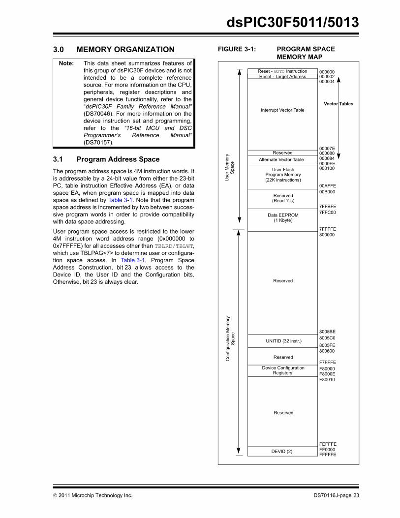
3.0 MEMORY ORGANIZATION
3.1 Program Address Space
The program address space is 4M instruction words. It
is addressable by a 24-bit value from either the 23-bit
PC, table instruction Effective Address (EA), or data
space EA, when program space is mapped into data
space as defined by Table 3-1. Note that the program
space address is incremented by two between succes-
sive program words in order to provide compatibility
with data space addressing.
User program space access is restricted to the lower
4M instruction word address range (0x000000 to
0x7FFFFE) for all accesses other than TBLRD/TBLWT,
which use TBLPAG<7> to determine user or configura-
tion space access. In Table 3-1, Program Space
Address Construction, bit 23 allows access to the
Device ID, the User ID and the Configuration bits.
Otherwise, bit 23 is always clear.
FIGURE 3-1: PROGRAM SPACE
MEMORY MAP Note: This data sheet summarizes features of
this group of dsPIC30F devices and is not
intended to be a complete reference
source. For more information on the CPU,
peripherals, register descriptions and
general device functionality, refer to the
“dsPIC30F Family Reference Manual”
(DS70046). For more information on the
device instruction set and programming,
refer to the “16-bit MCU and DSC
Programmer’s Reference Manual”
(DS70157).
Reset - Target Address
Use
r M
em
ory
Space
000000
00007E
000002
000080
Device Configuration
User FlashProgram Memory
00B000
00AFFE
Co
nfigu
ratio
n M
em
ory
Spa
ce
Data EEPROM
(22K instructions)
(1 Kbyte)
800000
F80000Registers F8000E
F80010
DEVID (2)
FEFFFE
FF0000FFFFFE
ReservedF7FFFE
Reserved
7FFC00
7FFBFE
(Read ‘0’s)
8005FE
800600
UNITID (32 instr.)
Vector Tables
8005BE
8005C0
Reset - GOTO Instruction
000004
Reserved
7FFFFE
Reserved
0001000000FE000084Alternate Vector Table
Reserved
Interrupt Vector Table
dsPIC30F5011/5013
DS70116J-page 24 2011 Microchip Technology Inc.
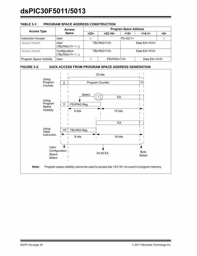
TABLE 3-1: PROGRAM SPACE ADDRESS CONSTRUCTION
FIGURE 3-2: DATA ACCESS FROM PROGRAM SPACE ADDRESS GENERATION
Access TypeAccess
Space
Program Space Address
<23> <22:16> <15> <14:1> <0>
Instruction Access User 0 PC<22:1> 0
TBLRD/TBLWT User
(TBLPAG<7> = 0)
TBLPAG<7:0> Data EA<15:0>
TBLRD/TBLWT Configuration
(TBLPAG<7> = 1)
TBLPAG<7:0> Data EA<15:0>
Program Space Visibility User 0 PSVPAG<7:0> Data EA<14:0>
0Program Counter
23 bits
1
PSVPAG Reg
8 bits
EA
15 bits
Program
Using
Select
TBLPAG Reg
8 bits
EA
16 bits
Using
Byte24-bit EA
0
0
1/0
Select
User/
Configuration
TableInstruction
ProgramSpace
Counter
Using
Space
Select
Visibility
Note: Program space visibility cannot be used to access bits <23:16> of a word in program memory.
2011 Microchip Technology Inc. DS70116J-page 25
dsPIC30F5011/5013
3.1.1 DATA ACCESS FROM PROGRAM
MEMORY USING TABLE
INSTRUCTIONS
This architecture fetches 24-bit wide program memory.
Consequently, instructions are always aligned.
However, as the architecture is modified Harvard, data
can also be present in program space.
There are two methods by which program space can
be accessed: via special table instructions, or through
the remapping of a 16K word program space page into
the upper half of data space (see Section 3.1.2 “Data
Access from Program Memory Using Program
Space Visibility”). The TBLRDL and TBLWTL instruc-
tions offer a direct method of reading or writing the least
significant word of any address within program space,
without going through data space. The TBLRDH and
TBLWTH instructions are the only method whereby the
upper 8 bits of a program space word can be accessed
as data.
The PC is incremented by two for each successive
24-bit program word. This allows program memory
addresses to directly map to data space addresses.
Program memory can thus be regarded as two 16-bit
word wide address spaces, residing side by side, each
with the same address range. TBLRDL and TBLWTL
access the space which contains the least significant
data word, and TBLRDH and TBLWTH access the space
which contains the Most Significant data Byte.
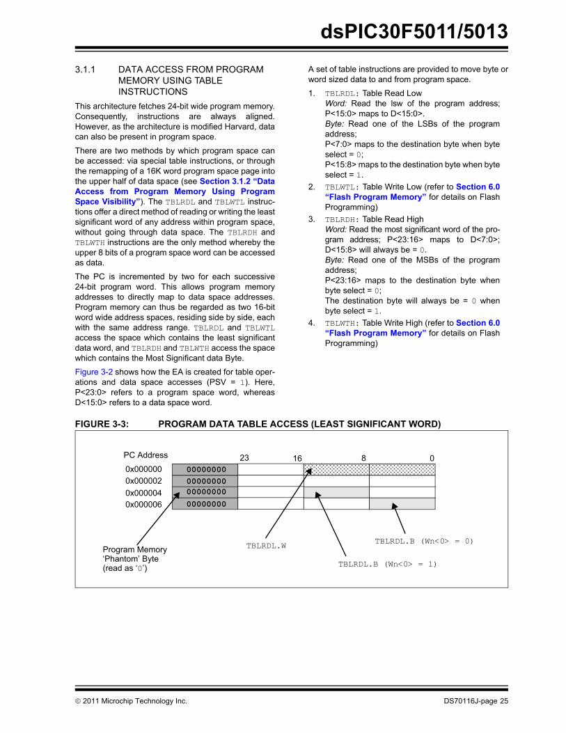
Figure 3-2 shows how the EA is created for table oper-
ations and data space accesses (PSV = 1). Here,
P<23:0> refers to a program space word, whereas
D<15:0> refers to a data space word.
A set of table instructions are provided to move byte or
word sized data to and from program space.
1. TBLRDL: Table Read Low
Word: Read the lsw of the program address;
P<15:0> maps to D<15:0>.
Byte: Read one of the LSBs of the program
address;
P<7:0> maps to the destination byte when byte
select = 0;
P<15:8> maps to the destination byte when byte
select = 1.
2. TBLWTL: Table Write Low (refer to Section 6.0
“Flash Program Memory” for details on Flash
Programming)
3. TBLRDH: Table Read High
Word: Read the most significant word of the pro-
gram address; P<23:16> maps to D<7:0>;
D<15:8> will always be = 0.
Byte: Read one of the MSBs of the program
address;
P<23:16> maps to the destination byte when
byte select = 0;
The destination byte will always be = 0 when
byte select = 1.
4. TBLWTH: Table Write High (refer to Section 6.0
“Flash Program Memory” for details on Flash
Programming)
FIGURE 3-3: PROGRAM DATA TABLE ACCESS (LEAST SIGNIFICANT WORD)
0816PC Address
0x000000
0x000002
0x000004
0x000006
23
00000000
00000000
00000000
00000000
Program Memory‘Phantom’ Byte(read as ‘0’)
TBLRDL.W
TBLRDL.B (Wn<0> = 1)
TBLRDL.B (Wn<0> = 0)