Embed Size (px)
Citation preview
Dual 1 A, 18 V, Synchronous Step-Down Regulator with Fail-Safe Voltage Monitoring
Data Sheet ADP2311
Rev. A Document Feedback Information furnished by Analog Devices is believed to be accurate and reliable. However, no responsibility is assumed by Analog Devices for its use, nor for any infringements of patents or other rights of third parties that may result from its use. Specifications subject to change without notice. No license is granted by implication or otherwise under any patent or patent rights of Analog Devices. Trademarks and registered trademarks are the property of their respective owners.
One Technology Way, P.O. Box 9106, Norwood, MA 02062-9106, U.S.A. Tel: 781.329.4700 ©2014 Analog Devices, Inc. All rights reserved. Technical Support www.analog.com
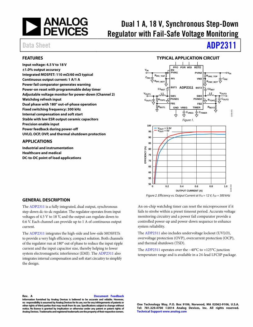
FEATURES Input voltage: 4.5 V to 18 V ±1.0% output accuracy Integrated MOSFET: 110 mΩ/60 mΩ typical Continuous output current: 1 A/1 A Power fail comparator generates warning Power-on reset with programmable delay timer Adjustable voltage monitor for power-down (Channel 2) Watchdog refresh input Dual phase with 180° out-of-phase operation Fixed switching frequency: 300 kHz Internal compensation and soft start Stable with low ESR output ceramic capacitors Precision enable input Power feedback during power-off UVLO, OCP, OVP, and thermal shutdown protection
APPLICATIONS Industrial and instrumentation Healthcare and medical DC-to-DC point of load applications
TYPICAL APPLICATION CIRCUIT
BST1
PVIN1
SW1
EN
FB1GND VREG
ADP2311
VIN
CIN1
PGND1
BST2
PVIN2
SW2
VM2
FB2
VIN
CIN2
PGND2
VOUT2L2
TIMER
PFO POR
PFI
CVREG CTIMER
WDI
RPFI_TOP
RPFI_BOT
RSTO
RVM2_TOP
RVM2_BOT
RTOP2
RBOT2
COUT2
C2BST
VOUT1 L1
RTOP1
RBOT1
COUT1
C1BST
1103
6-00
1
Figure 1.
50
55
60
65
70
75
80
85
90
95
100
0 0.2 0.4 0.6 0.8 1.0
EFFI
CIEN
CY (%
)
OUTPUT CURRENT (A)
VOUT = 3.3VVOUT = 5V
1103
6-00
2
Figure 2. Efficiency vs. Output Current at VIN = 12 V, fSW = 300 kHz
GENERAL DESCRIPTION The ADP2311 is a fully integrated, dual output, synchronous step-down dc-to-dc regulator. The regulator operates from input voltages of 4.5 V to 18 V, and the output can regulate down to 0.6 V. Each channel can provide up to 1 A of continuous output current.
The ADP2311 integrates the high-side and low-side MOSFETs to provide a very high efficiency, compact solution. Both channels of the regulator run at 180° out of phase to reduce the input ripple current and the input capacitor size, thereby helping to lower system electromagnetic interference (EMI). The ADP2311 also integrates internal compensation and soft start circuitry to simplify the design.
An on-chip watchdog timer can reset the microprocessor if it fails to strobe within a preset timeout period. Accurate voltage monitoring circuitry and a power fail comparator provide a controlled power-up and power-down sequence to enhance system reliability.
The ADP2311 also includes undervoltage lockout (UVLO), overvoltage protection (OVP), overcurrent protection (OCP), and thermal shutdown (TSD).
The ADP2311 operates over the −40°C to +125°C junction temperature range and is available in a 24-lead LFCSP package.
ADP2311* Product Page Quick LinksLast Content Update: 08/30/2016
Comparable PartsView a parametric search of comparable parts
Evaluation Kits• ADP2311 Evaluation Board
DocumentationData Sheet• ADP2311: Dual 1 A, 18 V, Synchronous Step-Down
Regulator with Fail-Safe Voltage Monitoring Data SheetUser Guides• UG-653: Evaluation Board for the ADP2311, Dual, 1 A, 18
V Synchronous Step-Down Regulator with Fail-Safe Voltage Monitoring
Tools and Simulations• ADIsimPower™ Voltage Regulator Design Tool
Design Resources• ADP2311 Material Declaration• PCN-PDN Information• Quality And Reliability• Symbols and Footprints
DiscussionsView all ADP2311 EngineerZone Discussions
Sample and BuyVisit the product page to see pricing options
Technical SupportSubmit a technical question or find your regional support number
* This page was dynamically generated by Analog Devices, Inc. and inserted into this data sheet. Note: Dynamic changes to the content on this page does not constitute a change to the revision number of the product data sheet. This content may be frequently modified.

ADP2311 Data Sheet
Rev. A | Page 2 of 20
TABLE OF CONTENTS Features .............................................................................................. 1 Applications ....................................................................................... 1 Typical Application Circuit ............................................................. 1 General Description ......................................................................... 1 Revision History ............................................................................... 2 Functional Block Diagram .............................................................. 3 Specifications ..................................................................................... 4 Absolute Maximum Ratings ............................................................ 6
Thermal Resistance ...................................................................... 6 ESD Caution .................................................................................. 6
Pin Configuration and Function Descriptions ............................. 7 Typical Performance Characteristics ............................................. 8 Theory of Operation ...................................................................... 13
Control Scheme .......................................................................... 13 Precision Enable/Shutdown ...................................................... 13 Internal Regulator (VREG) ....................................................... 13 Bootstrap Circuitry .................................................................... 13 Soft Start ...................................................................................... 13
Peak Current-Limit and Short-Circuit Protection ................ 13 Power-On Reset (POR) ............................................................. 13 TIMER Pin Configuration ........................................................ 14 Power Fail Comparator .............................................................. 15 Voltage Monitor Comparator (VM2) ...................................... 15 Watchdog Timer ......................................................................... 15 Power-Up and Power-Down Sequence ................................... 15 Overvoltage Protection (OVP) ................................................. 15 Undervoltage Lockout (UVLO) ............................................... 15 Thermal Shutdown .................................................................... 16
Applications Information .............................................................. 17 Input Capacitor Selection .......................................................... 17 Output Voltage Setting .............................................................. 17 Inductor Selection ...................................................................... 17 Output Capacitor Selection....................................................... 18
Application Circuit ......................................................................... 19 Outline Dimensions ....................................................................... 20
Ordering Guide .......................................................................... 20
REVISION HISTORY 3/14—Revision A: Initial Version
Data Sheet ADP2311
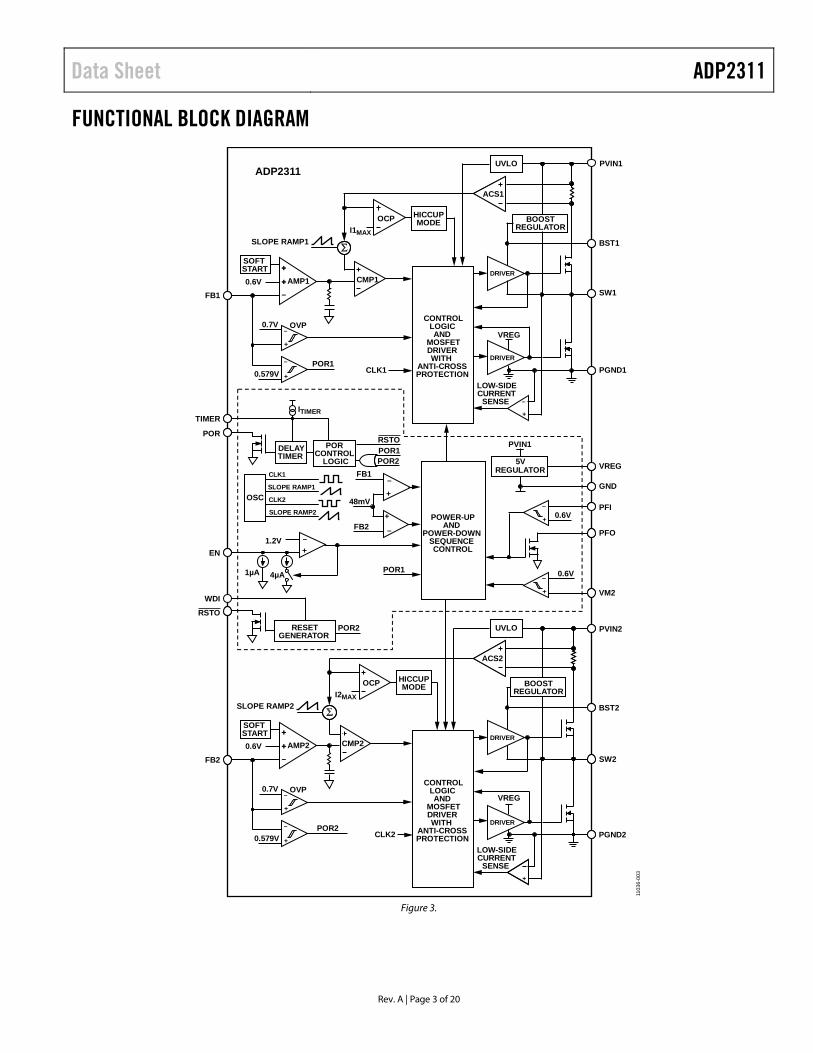
Rev. A | Page 3 of 20
FUNCTIONAL BLOCK DIAGRAM
+0.6V AMP1
CONTROLLOGICAND
MOSFETDRIVERWITH
ANTI-CROSSPROTECTION
BST1
SW1
I1MAX
HICCUPMODE
DRIVER
VREG+
–
–
–
OVP
PVIN1UVLO
PGND1
SLOPE RAMP1
CLK1
LOW-SIDECURRENT
SENSE
+
SOFTSTART
+0.579V
ITIMER
DELAYTIMER
POR1
POR1POR2
PFO
0.6V
0.6V
PFI
VM2
POR2
–+
1.2V
1µA 4µA
POWER-UPAND
POWER-DOWNSEQUENCECONTROL
VREG
PVIN1
GND
5VREGULATOR
OSC
CLK1
CLK2
SLOPE RAMP1
SLOPE RAMP2
FB2
FB1
ADP2311
POR1
+48mV
+
PORCONTROL
LOGIC
ACS1
–
+DRIVER
+
+
RESETGENERATOR
–
–
ACS1
OCP
CMP1
0.7V
BOOSTREGULATOR
+0.6V AMP2
CONTROLLOGICAND
MOSFETDRIVERWITH
ANTI-CROSSPROTECTION
BST2
SW2
I2MAX
HICCUPMODE
DRIVER
VREG+
–
–
OVP
PVIN2UVLO
PGND2
SLOPE RAMP2
CLK2
LOW-SIDECURRENT
SENSE
+
SOFTSTART
+0.579VPOR2
ACS1
–
+DRIVER
+
–
+
–
+
+
ACS2
OCP
CMP2
0.7V
BOOSTREGULATOR
FB1
TIMER
FB2
POR
WDI
EN
1103
6-00
3
RSTO
RSTO
Figure 3.
ADP2311 Data Sheet
Rev. A | Page 4 of 20
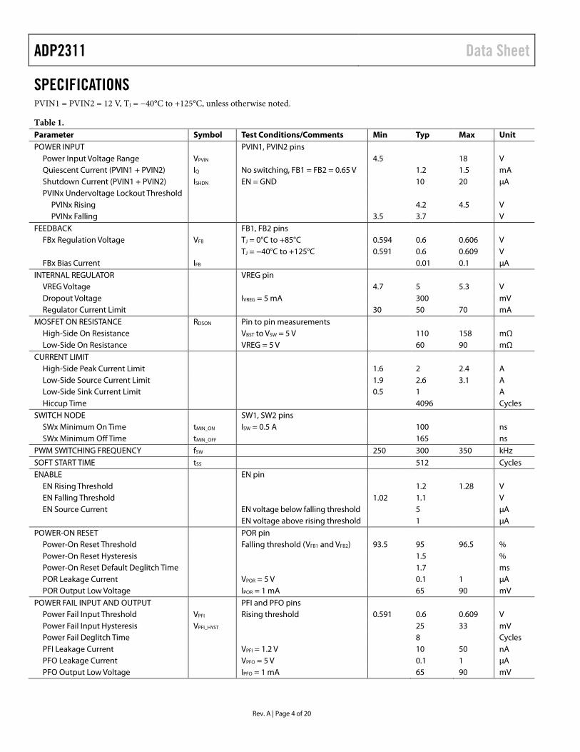
SPECIFICATIONS PVIN1 = PVIN2 = 12 V, TJ = −40°C to +125°C, unless otherwise noted.
Table 1. Parameter Symbol Test Conditions/Comments Min Typ Max Unit POWER INPUT PVIN1, PVIN2 pins
Power Input Voltage Range VPVIN 4.5 18 V Quiescent Current (PVIN1 + PVIN2) IQ No switching, FB1 = FB2 = 0.65 V 1.2 1.5 mA Shutdown Current (PVIN1 + PVIN2) ISHDN EN = GND 10 20 µA PVINx Undervoltage Lockout Threshold
PVINx Rising 4.2 4.5 V PVINx Falling 3.5 3.7 V
FEEDBACK FB1, FB2 pins FBx Regulation Voltage VFB TJ = 0°C to +85°C 0.594 0.6 0.606 V
TJ = −40°C to +125°C 0.591 0.6 0.609 V FBx Bias Current IFB 0.01 0.1 µA
INTERNAL REGULATOR VREG pin VREG Voltage 4.7 5 5.3 V Dropout Voltage IVREG = 5 mA 300 mV Regulator Current Limit 30 50 70 mA
MOSFET ON RESISTANCE RDSON Pin to pin measurements High-Side On Resistance VBST to VSW = 5 V 110 158 mΩ Low-Side On Resistance VREG = 5 V 60 90 mΩ
CURRENT LIMIT High-Side Peak Current Limit 1.6 2 2.4 A Low-Side Source Current Limit 1.9 2.6 3.1 A Low-Side Sink Current Limit 0.5 1 A Hiccup Time 4096 Cycles
SWITCH NODE SW1, SW2 pins SWx Minimum On Time tMIN_ON ISW = 0.5 A 100 ns SWx Minimum Off Time tMIN_OFF 165 ns
PWM SWITCHING FREQUENCY fSW 250 300 350 kHz SOFT START TIME tSS 512 Cycles ENABLE EN pin
EN Rising Threshold 1.2 1.28 V EN Falling Threshold 1.02 1.1 V EN Source Current EN voltage below falling threshold 5 µA
EN voltage above rising threshold 1 µA POWER-ON RESET POR pin
Power-On Reset Threshold Falling threshold (VFB1 and VFB2) 93.5 95 96.5 % Power-On Reset Hysteresis 1.5 % Power-On Reset Default Deglitch Time 1.7 ms POR Leakage Current VPOR = 5 V 0.1 1 µA POR Output Low Voltage IPOR = 1 mA 65 90 mV
POWER FAIL INPUT AND OUTPUT PFI and PFO pins Power Fail Input Threshold VPFI Rising threshold 0.591 0.6 0.609 V Power Fail Input Hysteresis VPFI_HYST 25 33 mV Power Fail Deglitch Time 8 Cycles PFI Leakage Current VPFI = 1.2 V 10 50 nA PFO Leakage Current VPFO = 5 V 0.1 1 µA PFO Output Low Voltage IPFO = 1 mA 65 90 mV
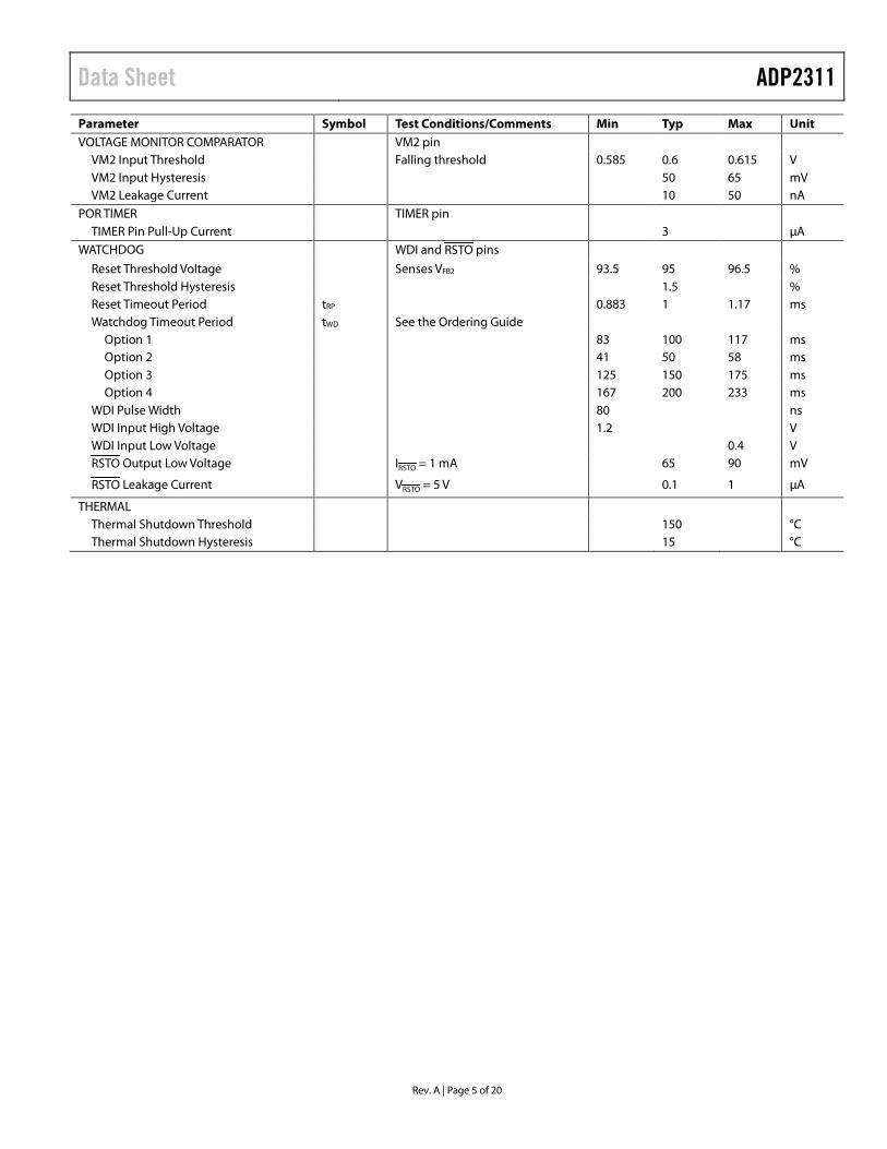
Data Sheet ADP2311
Rev. A | Page 5 of 20
Parameter Symbol Test Conditions/Comments Min Typ Max Unit VOLTAGE MONITOR COMPARATOR VM2 pin
VM2 Input Threshold Falling threshold 0.585 0.6 0.615 V VM2 Input Hysteresis 50 65 mV VM2 Leakage Current 10 50 nA
POR TIMER TIMER pin TIMER Pin Pull-Up Current 3 µA
WATCHDOG WDI and RSTO pins
Reset Threshold Voltage Senses VFB2 93.5 95 96.5 % Reset Threshold Hysteresis 1.5 % Reset Timeout Period tRP 0.883 1 1.17 ms Watchdog Timeout Period tWD See the Ordering Guide
Option 1 83 100 117 ms Option 2 41 50 58 ms Option 3 125 150 175 ms Option 4 167 200 233 ms
WDI Pulse Width 80 ns WDI Input High Voltage 1.2 V WDI Input Low Voltage 0.4 V RSTO Output Low Voltage IRSTO = 1 mA 65 90 mV
RSTO Leakage Current VRSTO = 5 V 0.1 1 µA
THERMAL Thermal Shutdown Threshold 150 °C Thermal Shutdown Hysteresis 15 °C
ADP2311 Data Sheet
Rev. A | Page 6 of 20
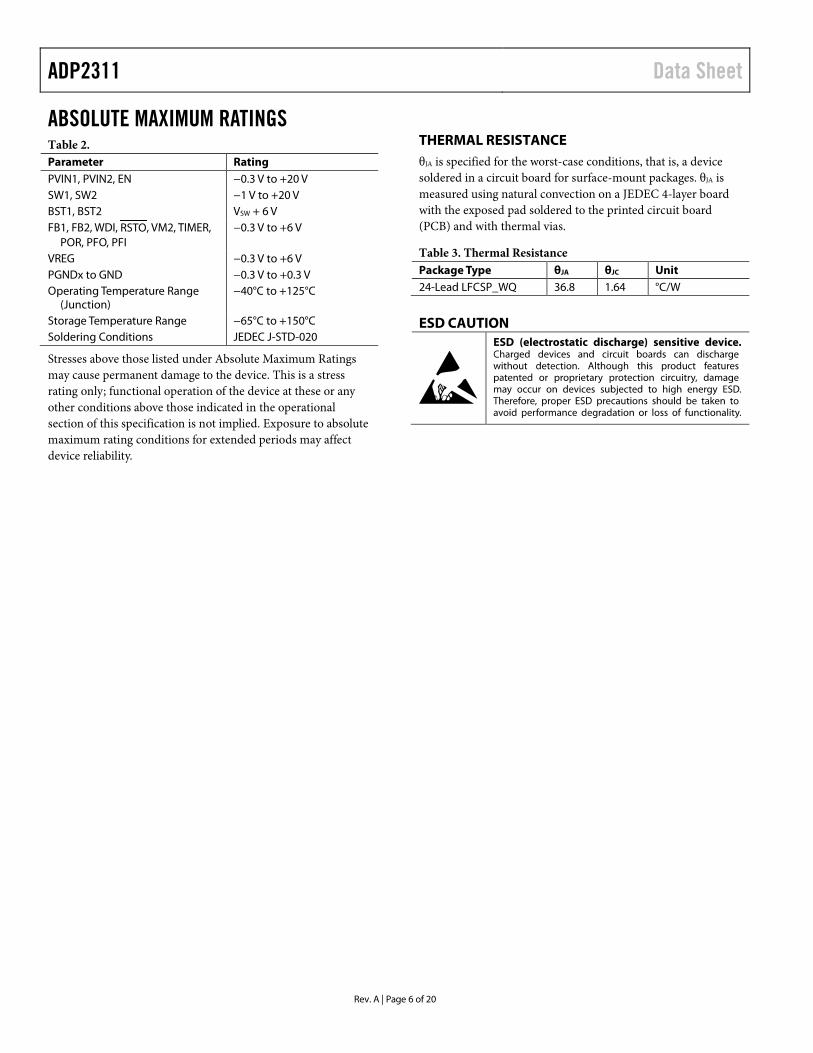
ABSOLUTE MAXIMUM RATINGS Table 2. Parameter Rating PVIN1, PVIN2, EN −0.3 V to +20 V SW1, SW2 −1 V to +20 V BST1, BST2 VSW + 6 V FB1, FB2, WDI, RSTO, VM2, TIMER,
POR, PFO, PFI −0.3 V to +6 V
VREG −0.3 V to +6 V PGNDx to GND −0.3 V to +0.3 V Operating Temperature Range
(Junction) −40°C to +125°C
Storage Temperature Range −65°C to +150°C Soldering Conditions JEDEC J-STD-020
Stresses above those listed under Absolute Maximum Ratings may cause permanent damage to the device. This is a stress rating only; functional operation of the device at these or any other conditions above those indicated in the operational section of this specification is not implied. Exposure to absolute maximum rating conditions for extended periods may affect device reliability.
THERMAL RESISTANCE θJA is specified for the worst-case conditions, that is, a device soldered in a circuit board for surface-mount packages. θJA is measured using natural convection on a JEDEC 4-layer board with the exposed pad soldered to the printed circuit board (PCB) and with thermal vias.
Table 3. Thermal Resistance Package Type θJA θJC Unit 24-Lead LFCSP_WQ 36.8 1.64 °C/W
ESD CAUTION
Data Sheet ADP2311
Rev. A | Page 7 of 20
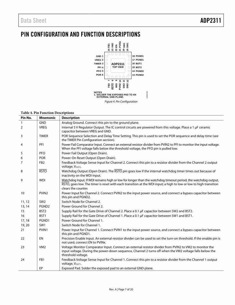
PIN CONFIGURATION AND FUNCTION DESCRIPTIONS
GNDVREG
POR
TIMER
PFO
PGND1
NOTES1. SOLDER THE EXPOSED PAD TO AN EXTERNAL GND PLANE.
SW2
PVIN
2W
DI
FB2
SW2
PVIN
1ENFB
1
SW1
SW1
VM2
PFI
21
3456
181716151413
8 9 10 117 1220 1921222324
ADP2311TOP VIEW
RST
O
PGND1BST1BST2PGND2PGND2
1103
6-00
4
Figure 4. Pin Configuration
Table 4. Pin Function Descriptions Pin No. Mnemonic Description 1 GND Analog Ground. Connect this pin to the ground plane. 2 VREG Internal 5 V Regulator Output. The IC control circuits are powered from this voltage. Place a 1 µF ceramic
capacitor between VREG and GND. 3 TIMER POR Sequence Selection and Delay Time Setting. This pin is used to set the POR sequence and delay time (see
the TIMER Pin Configuration section). 4 PFI Power Fail Comparator Input. Connect an external resistor divider from PVIN2 to PFI to monitor the input voltage.
When the PFI voltage falls below the threshold voltage, the PFO pin is pulled low. 5 PFO Power Fail Output (Open Drain). 6 POR Power-On Reset Output (Open Drain). 7 FB2 Feedback Voltage Sense Input for Channel 2. Connect this pin to a resistor divider from the Channel 2 output
voltage, VOUT2. 8 RSTO Watchdog Output (Open Drain). The RSTO pin goes low if the internal watchdog timer times out because of
inactivity on the WDI input. 9 WDI Watchdog Input. If WDI remains high or low for longer than the watchdog timeout period, the watchdog output,
RSTO, goes low. The timer is reset with each transition at the WDI input; a high to low or low to high transition clears the counter.
10 PVIN2 Power Input for Channel 2. Connect PVIN2 to the input power source, and connect a bypass capacitor between this pin and PGND2.
11, 12 SW2 Switch Node for Channel 2. 13, 14 PGND2 Power Ground for Channel 2. 15 BST2 Supply Rail for the Gate Drive of Channel 2. Place a 0.1 µF capacitor between SW2 and BST2. 16 BST1 Supply Rail for the Gate Drive of Channel 1. Place a 0.1 µF capacitor between SW1 and BST1. 17, 18 PGND1 Power Ground for Channel 1. 19, 20 SW1 Switch Node for Channel 1. 21 PVIN1 Power Input for Channel 1. Connect PVIN1 to the input power source, and connect a bypass capacitor between
this pin and PGND1. 22 EN Precision Enable Input. An external resistor divider can be used to set the turn-on threshold. If the enable pin is
not used, connect EN to PVINx. 23 VM2 Voltage Monitor Comparator Input. Connect an external resistor divider from PVIN2 to VM2 to monitor the
input voltage. During the power-down sequence, Channel 2 turns off when the VM2 voltage falls below the threshold voltage.
24 FB1 Feedback Voltage Sense Input for Channel 1. Connect this pin to a resistor divider from the Channel 1 output voltage, VOUT1.
EP Exposed Pad. Solder the exposed pad to an external GND plane.
ADP2311 Data Sheet
Rev. A | Page 8 of 20
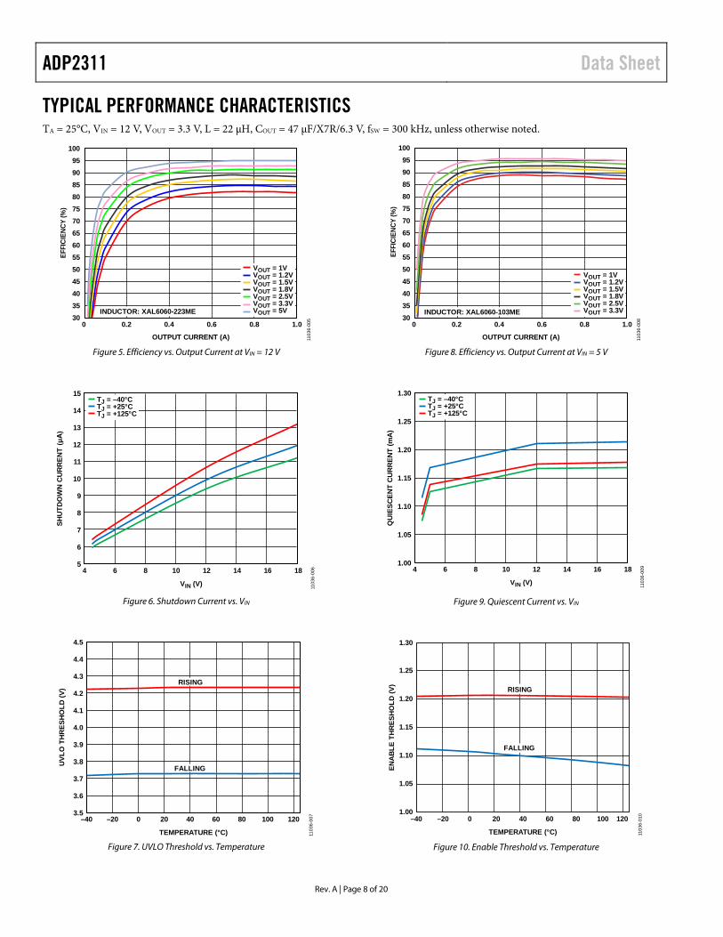
TYPICAL PERFORMANCE CHARACTERISTICS TA = 25°C, VIN = 12 V, VOUT = 3.3 V, L = 22 µH, COUT = 47 µF/X7R/6.3 V, fSW = 300 kHz, unless otherwise noted.
3035404550556065707580859095
100
0 0.2 0.4 0.6 0.8 1.0
EFFI
CIEN
CY (%
)
OUTPUT CURRENT (A)
INDUCTOR: XAL6060-223ME
VOUT = 1VVOUT = 1.2VVOUT = 1.5VVOUT = 1.8VVOUT = 2.5VVOUT = 3.3VVOUT = 5V
1103
6-00
5
Figure 5. Efficiency vs. Output Current at VIN = 12 V
5
6
7
8
9
10
11
12
13
14
15
4 6 8 10 12 14 16 18
SHU
TDO
WN
CU
RR
ENT
(μA
)
VIN (V)
TJ = –40°CTJ = +25°CTJ = +125°C
1103
6-00
6
Figure 6. Shutdown Current vs. VIN
3.5
3.6
3.7
3.8
3.9
4.0
4.1
4.2
4.3
4.4
4.5
–40 –20 0 20 40 60 80 100 120
UVL
O T
HR
ESH
OLD
(V)
RISING
FALLING
TEMPERATURE (°C) 1103
6-00
7
Figure 7. UVLO Threshold vs. Temperature
0 0.2 0.4 0.6 0.8 1.0
OUTPUT CURRENT (A)
3035404550556065707580859095
100
EFFI
CIEN
CY (%
)
INDUCTOR: XAL6060-103ME
1103
6-00
8
VOUT = 1VVOUT = 1.2VVOUT = 1.5VVOUT = 1.8VVOUT = 2.5VVOUT = 3.3V
Figure 8. Efficiency vs. Output Current at VIN = 5 V
1.00
1.05
1.10
1.15
1.20
1.25
1.30
4 6 8 10 12 14 16 18
QU
IESC
ENT
CU
RR
ENT
(mA
)
VIN (V)
TJ = –40°CTJ = +25°CTJ = +125°C
1103
6-00
9
Figure 9. Quiescent Current vs. VIN
1.00
1.05
1.10
1.15
1.20
1.25
1.30
–40 –20 0 20 40 60 80 100 120
ENA
BLE
TH
RES
HO
LD (V
)
TEMPERATURE (°C) 1103
6-01
0
RISING
FALLING
Figure 10. Enable Threshold vs. Temperature
Data Sheet ADP2311
Rev. A | Page 9 of 20
4.2
4.4
4.6
4.8
5.0
5.2
5.4
–40 –20 0 20 40 60 80 100 120
EN S
OU
RC
E C
UR
REN
T(µ
A)
TEMPERATURE (°C) 1103
6-01
1
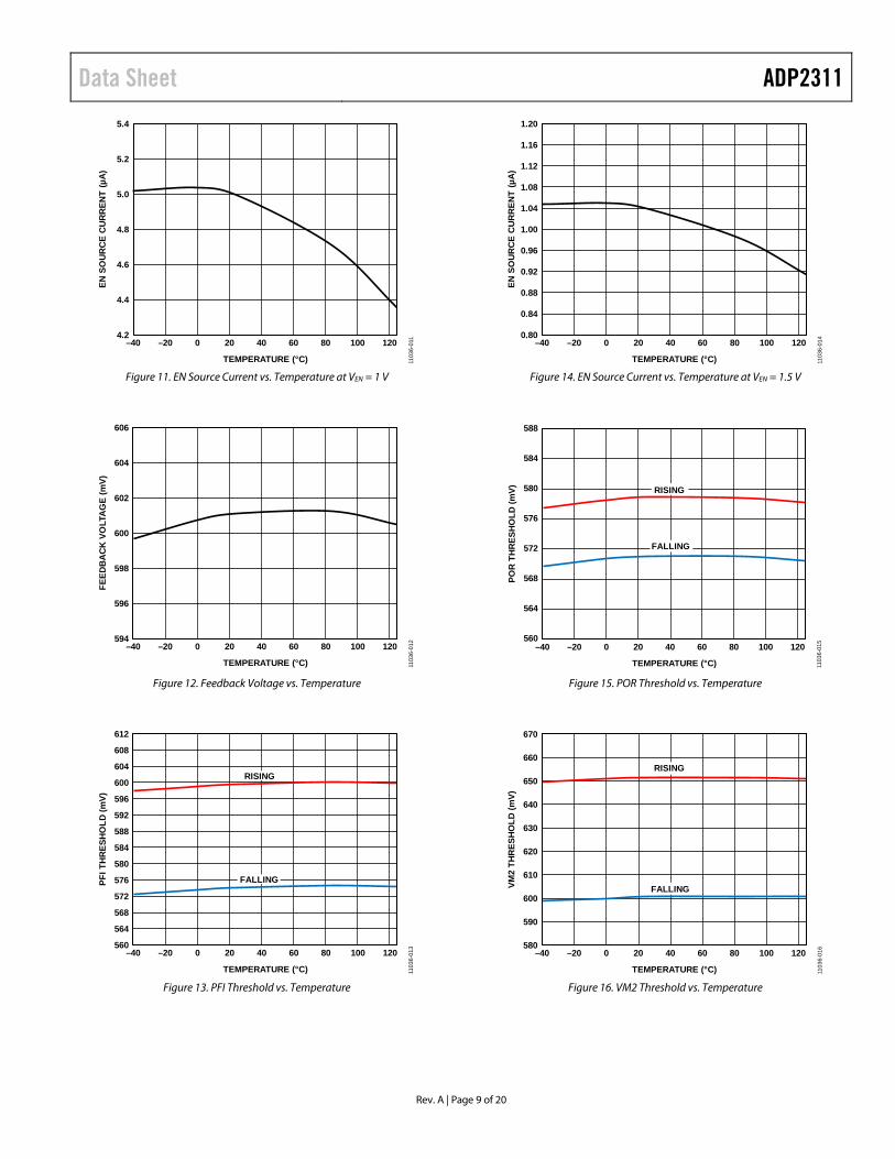
Figure 11. EN Source Current vs. Temperature at VEN = 1 V
594
596
598
600
602
604
606
–40 –20 0 20 40 60 80 100 120
FEED
BA
CK
VO
LTA
GE
(mV)
TEMPERATURE (°C) 1103
6-01
2
Figure 12. Feedback Voltage vs. Temperature
560
564
568
572
576
580
584
588
592
596
600
604
608
612
–40 –20 0 20 40 60 80 100 120
PFI T
HR
ESH
OLD
(mV)
TEMPERATURE (°C)
RISING
FALLING
1103
6-01
3
Figure 13. PFI Threshold vs. Temperature
0.80
0.84
0.88
0.92
0.96
1.00
1.04
1.08
1.12
1.16
1.20
–40 –20 0 20 40 60 80 100 120
EN S
OU
RC
E C
UR
REN
T(µ
A)
TEMPERATURE (°C) 1103
6-01
4
Figure 14. EN Source Current vs. Temperature at VEN = 1.5 V
560
564
568
572
576
580
584
588
–40 –20 0 20 40 60 80 100 120
POR
TH
RES
HO
LD (m
V) RISING
FALLING
TEMPERATURE (°C) 1103
6-01
5
Figure 15. POR Threshold vs. Temperature
580
590
600
610
620
630
640
650
660
670
–40 –20 0 20 40 60 80 100 120
VM2
THR
ESH
OLD
(mV)
RISING
FALLING
TEMPERATURE (°C) 1103
6-01
6
Figure 16. VM2 Threshold vs. Temperature
ADP2311 Data Sheet
Rev. A | Page 10 of 20
250
260
270
280
290
300
310
320
330
340
350
–40 –20 0 20 40 60 80 100 120
FREQ
UEN
CY
(kH
z)
TEMPERATURE (°C) 1103
6-01
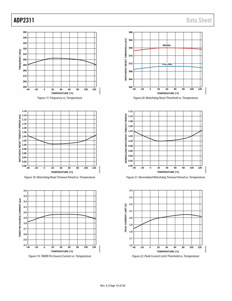
7Figure 17. Frequency vs. Temperature
0.90
0.92
0.94
0.96
0.98
1.00
1.02
1.04
1.06
1.08
1.10
1.12
1.14
1.16
–40 –20 0 20 40 60 80 100 120
WAT
CH
DO
G R
ESET
TIM
EOU
T PE
RIO
D (m
s)
TEMPERATURE (°C) 1103
6-01
8
Figure 18. Watchdog Reset Timeout Period vs. Temperature
2.4
2.5
2.6
2.7
2.8
2.9
3.0
3.1
3.2
3.3
3.4
–40 –20 0 20 40 60 80 100 120
TIM
ER P
IN S
OU
RC
E C
UR
REN
T (µ
A)
TEMPERATURE (°C) 1103
6-01
9
Figure 19. TIMER Pin Source Current vs. Temperature
560
564
568
572
576
580
584
588
–40 –20 0 20 40 60 80 100 120
WAT
CH
DO
G R
ESET
TH
RES
HO
LD (m
V)
TEMPERATURE (°C)
RISING
FALLING
1103
6-02
0
Figure 20. Watchdog Reset Threshold vs. Temperature
0.90
0.92
0.94
0.96
0.98
1.00
1.02
1.04
1.06
1.08
1.10
1.12
–40 –20 0 20 40 60 80 100 120
NO
RM
ALI
ZED
WAT
CH
DO
G T
IMEO
UT
PER
IOD
TEMPERATURE (°C) 1103
6-02
1
Figure 21. Normalized Watchdog Timeout Period vs. Temperature
1.6
1.7
1.8
1.9
2.0
2.1
2.2
2.3
2.4
–40 –20 0 20 40 60 80 100 120
PEA
K C
UR
REN
T LI
MIT
(A)
TEMPERATURE (°C) 1103
6-02
2
Figure 22. Peak Current Limit Threshold vs. Temperature
Data Sheet ADP2311
Rev. A | Page 11 of 20
50
60
70
80
90
100
110
120
130
140
150
160
–40 –20 0 20 40 60 80 100 120
MO
SFET
RES
ISTO
R (m
Ω)
TEMPERATURE (°C) 1103
6-02
3
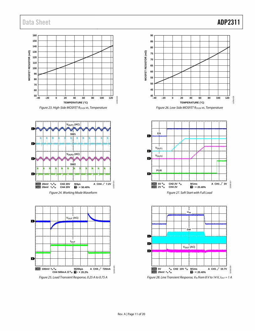
Figure 23. High-Side MOSFET RDSON vs. Temperature
CH1 20mV CH2 20V M4µs A CH4 7.2V
1
2
3
4
T 50.40%BW
CH3 20mV CH4 20VBW 1103
6-02
4
VOUT1 (AC)
SW1
VOUT2 (AC)
SW2
Figure 24. Working Mode Waveform
CH1 100mV M200µs A CH4 720mA
1
4
T 20.2%BW
BWCH4 500mA Ω 1103
6-02
5
VOUT (AC)
IOUT
Figure 25. Load Transient Response, 0.25 A to 0.75 A
40
45
50
55
60
65
70
75
80
85
90
–40 –20 0 20 40 60 80 100 120
MO
SFET
RES
ISTO
R (m
Ω)
TEMPERATURE (°C) 1103
6-02
6
Figure 26. Low-Side MOSFET RDSON vs. Temperature
CH1 5V CH2 2V M1ms A CH1 3V
1
2
3
4
T 20.40%BW BW
CH3 2V CH4 2VBW 1103
6-02
7
EN
VOUT2
POR
VOUT1
Figure 27. Soft Start with Full Load
CH1 5V CH2 10V M1ms A CH1 10.7V
1
2
3
T 20.40%BW BW
CH3 20mV BW 1103
6-02
8
VIN
SW
VOUT (AC)
Figure 28. Line Transient Response, VIN from 8 V to 14 V, IOUT = 1 A

ADP2311 Data Sheet
Rev. A | Page 12 of 20
CH1 2VCH4 2ACH2 10V M10ms A CH1 2.04V
1
2
4
T 20.2%BW
BWBWΩ 11
036-
029
VOUT
SW
IL
Figure 29. Output Short
CH1 2V CH2 10V M10ms A CH1 2.04V
1
2
4
T 70.40%BW BW
BWCH4 2A Ω 1103
6-03
0
VOUT
SW
IL
Figure 30. Output Short Recovery
Data Sheet ADP2311
Rev. A | Page 13 of 20
THEORY OF OPERATION The ADP2311 is a fully integrated, dual output, step-down dc-to-dc regulator. The ADP2311 can operate with an input voltage from 4.5 V to 18 V and can regulate the output voltage down to 0.6 V. The ADP2311 also integrates power-up and power-down sequence circuitry and a watchdog timer to enhance system reliability.
CONTROL SCHEME The ADP2311 features a fixed frequency, current mode pulse-width modulation (PWM) control architecture. At the start of each oscillator cycle, the high-side MOSFET turns on, placing a positive voltage across the inductor. The inductor current increases until the current sense signal crosses the peak inductor current threshold, which turns off the high-side MOSFET and turns on the low-side MOSFET. This places a negative voltage across the inductor, reducing the inductor current. The low-side MOSFET stays on for the remainder of the cycle.
PRECISION ENABLE/SHUTDOWN The ADP2311 has a precision enable pin for both channels. The EN pin has an internal pull-down current source of 5 µA that provides a default turn-off when the EN pin is open.
When the voltage on the EN pin exceeds 1.2 V typical, Channel 1 and Channel 2 are enabled, and the internal pull-down current source at the EN pin is reduced to 1 µA, which allows the user to program the input voltage UVLO.
When the voltage on the EN pin falls below 1.1 V typical, Channel 1, Channel 2, and all internal circuits are turned off, and the device enters shutdown mode.
INTERNAL REGULATOR (VREG) The internal regulator provides a stable voltage supply for the internal control circuits and bias voltage for the low-side gate drivers. It is recommended that a 1 µF ceramic capacitor be placed between VREG and GND. The internal regulator also includes a current-limit circuit for protection.
The PVIN1 pin provides the power supply for the internal regulator shared by both channels.
BOOTSTRAP CIRCUITRY The ADP2311 integrates boot regulators to provide the gate drive voltage for the high-side MOSFETs. The regulators generate 5 V bootstrap voltages between the BSTx pin and the SWx pin.
It is recommended that an X7R or X5R, 0.1 µF ceramic capacitor be placed between the BSTx and the SWx pins.
SOFT START The ADP2311 has integrated soft start circuitry to limit the output voltage rise time and to reduce inrush current at startup. The soft start time is fixed at 512 clock cycles (1.7 ms).
PEAK CURRENT-LIMIT AND SHORT-CIRCUIT PROTECTION The ADP2311 has a peak current-limit protection circuit to prevent current runaway. The high-side MOSFET peak current is limited to 2 A typical. When the peak inductor current reaches the current-limit threshold, the high-side MOSFET turns off, the low-side MOSFET turns on, and the overcurrent counter increments.
When the low-side MOSFET is turned on, the internal circuit continues to monitor the current going through the low-side MOSFET. At the end of every clock cycle, if the low-side MOSFET source current is greater than the low-side source current limit threshold (2.6 A typical), the high-side MOSFET stays off, the low-side MOSFET stays on for the next cycle, and the over-current counter increments. The high-side MOSFET turns on again when the low-side source current is below the low-side source current limit at the start of a cycle.
If the high-side MOSFET peak current does not exceed the peak current limit in one cycle, the overcurrent counter is reset. If the overcurrent counter reaches 10, the device enters hiccup mode. During hiccup mode, the high-side and low-side MOSFETs are both turned off. The device remains in hiccup mode for 4096 clock cycles and then attempts a soft start. If the current-limit fault is cleared, the device resumes normal operation; if the current-limit fault is still active, the device reenters hiccup mode.
The low-side MOSFET can also sink current from the load. If the low-side sink current limit is exceeded, both the low-side and high-side MOSFETs are turned off until the next cycle starts.
POWER-ON RESET (POR) The POR pin is an active high, open-drain output that requires a resistor to pull it up to a voltage.
The POR threshold is referenced to the FBx pin voltage (VFB) and is specified as a percentage of VFB. The POR falling threshold is 95% typical, 93.5% minimum, and 96.5% maximum, which covers the full temperature range. Therefore, the typical POR falling threshold is 95% of the typical VFB value, the minimum POR falling threshold is 93.5% of the minimum VFB value, and the maximum POR falling threshold is 96.5% of the maximum VFB value.
If VFB is at the minimum value of 0.591 V, the minimum voltage of the POR falling threshold is 0.591 V × 93.5% = 0.553 V.
If VFB is at the maximum value of 0.609 V, the maximum voltage of the POR falling threshold is 0.609 V × 96.5% = 0.588 V.
Therefore, the worst-case POR falling threshold voltage range is 0.553 V to 0.588 V.
The typical POR falling threshold voltage is 0.6 V × 95% = 0.57 V.
ADP2311 Data Sheet
Rev. A | Page 14 of 20
The POR function has hysteresis of 1.5% between the falling and rising thresholds. The POR rising threshold is 96.5% typical, 95% minimum, and 98% maximum. Therefore, the typical POR rising trigger voltage is 0.6 V × 96.5% = 0.579 V. The POR rising threshold voltage is always higher than the POR falling threshold voltage.
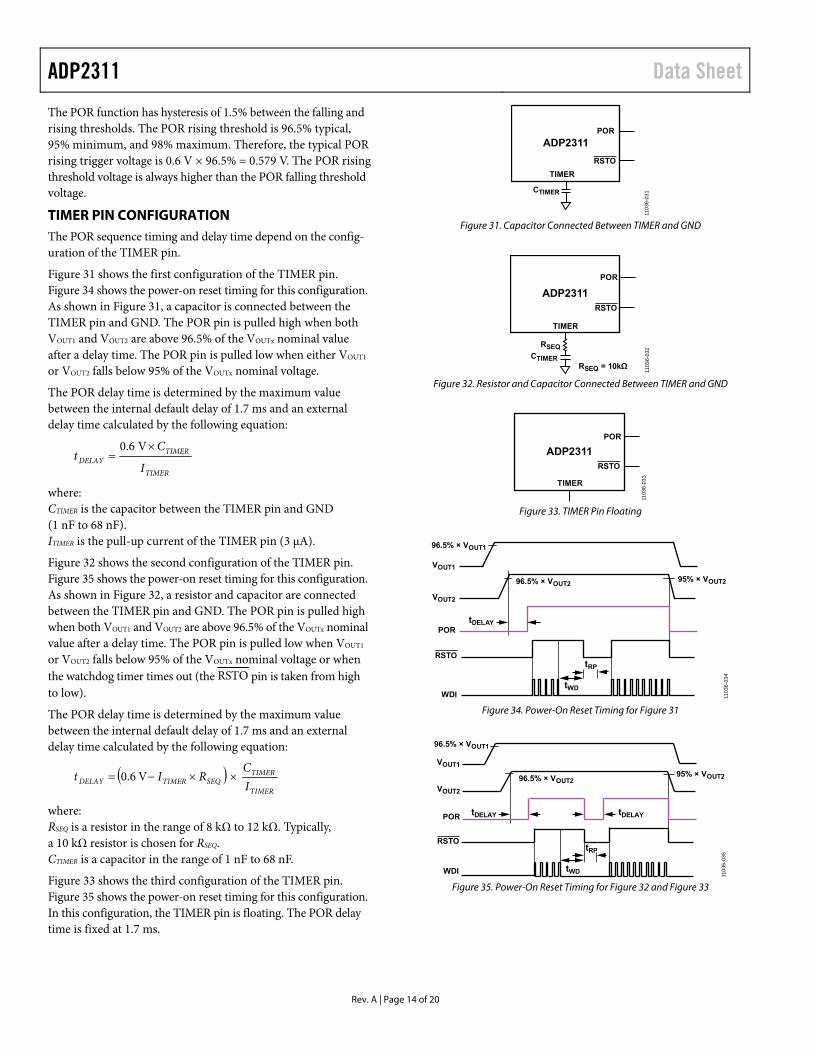
TIMER PIN CONFIGURATION The POR sequence timing and delay time depend on the config-uration of the TIMER pin.
Figure 31 shows the first configuration of the TIMER pin. Figure 34 shows the power-on reset timing for this configuration. As shown in Figure 31, a capacitor is connected between the TIMER pin and GND. The POR pin is pulled high when both VOUT1 and VOUT2 are above 96.5% of the VOUTx nominal value after a delay time. The POR pin is pulled low when either VOUT1 or VOUT2 falls below 95% of the VOUTx nominal voltage.
The POR delay time is determined by the maximum value between the internal default delay of 1.7 ms and an external delay time calculated by the following equation:
TIMER
TIMERDELAY
I
Ct
V0.6
where: CTIMER is the capacitor between the TIMER pin and GND (1 nF to 68 nF). ITIMER is the pull-up current of the TIMER pin (3 μA).
Figure 32 shows the second configuration of the TIMER pin. Figure 35 shows the power-on reset timing for this configuration. As shown in Figure 32, a resistor and capacitor are connected between the TIMER pin and GND. The POR pin is pulled high when both VOUT1 and VOUT2 are above 96.5% of the VOUTx nominal value after a delay time. The POR pin is pulled low when VOUT1 or VOUT2 falls below 95% of the VOUTx nominal voltage or when the watchdog timer times out (the RSTO pin is taken from high to low).
The POR delay time is determined by the maximum value between the internal default delay of 1.7 ms and an external delay time calculated by the following equation:
TIMER
TIMERSEQTIMERDELAY I
CRIt V6.0
where: RSEQ is a resistor in the range of 8 kΩ to 12 kΩ. Typically, a 10 kΩ resistor is chosen for RSEQ. CTIMER is a capacitor in the range of 1 nF to 68 nF.
Figure 33 shows the third configuration of the TIMER pin. Figure 35 shows the power-on reset timing for this configuration. In this configuration, the TIMER pin is floating. The POR delay time is fixed at 1.7 ms.
ADP2311
TIMER
CTIMER
POR
1103
6-03
1
RSTO
Figure 31. Capacitor Connected Between TIMER and GND
CTIMER
ADP2311
TIMER
RSEQ
POR
RSEQ = 10kΩ
1103
6-03
2
RSTO
Figure 32. Resistor and Capacitor Connected Between TIMER and GND
ADP2311
TIMER
POR
1103
6-03
3
RSTO
Figure 33. TIMER Pin Floating
VOUT1
tWDWDI
VOUT2
PORtDELAY
96.5% × VOUT1
96.5% × VOUT295% × VOUT2
1103
6-03
4
tRP
RSTO
Figure 34. Power-On Reset Timing for Figure 31
WDI
VOUT2
POR
tWD
tRP
VOUT1
tDELAYtDELAY
96.5% × VOUT1
96.5% × VOUT295% × VOUT2
1103
6-03
5
RSTO
Figure 35. Power-On Reset Timing for Figure 32 and Figure 33

Data Sheet ADP2311
Rev. A | Page 15 of 20
POWER FAIL COMPARATOR The ADP2311 integrates a power fail comparator that can generate a warning when the input voltage falls below the designated voltage. When the PFI input voltage falls below 0.575 V, the PFO pin is pulled low. When the PFI input voltage rises above 0.6 V, the PFO pin is pulled high. The low leakage current of the PFI pin allows the use of a large value external resistor to reduce system current consumption.
The PFO pin can be used to send a warning signal to the pro-cessor in case of an abnormal input voltage condition so that the processor can prepare to power down the system before power is lost.
VOLTAGE MONITOR COMPARATOR (VM2) The VM2 pin connects to an accurate comparator. When the VM2 voltage falls below 0.6 V, Channel 2 is turned off. When the VM2 voltage rises above 0.65 V, Channel 2 is allowed to power up if the EN pin is high and PFI is above 0.6 V.
WATCHDOG TIMER The watchdog timer circuit is used to monitor the activity of the processor. During power-up, the watchdog timer circuit does not acknowledge pulses from the WDI pin until the voltage at FB2 is above the reset threshold and the reset timeout period (tRP) has elapsed. During the power-up sequence, the RSTO pin is pulled low and remains low until the watchdog timer circuit is activated. The watchdog timer circuit can be initialized only by a low to high transition on the WDI pin both after power up and after a watchdog timeout (see Figure 36).
VOUT2
96.5%
tRP tWD tRP
WDI 1103
6-03
6
RSTO
Figure 36. Watchdog Timing Diagram
After the watchdog timer circuit is active, it is cleared with every low to high or high to low logic transition on the WDI pin, which can detect pulse widths as short as 80 ns. If the WDI pin remains high or low for longer than the watchdog timeout period (tWD), a reset is asserted, and the RSTO pin is pulled low. The processor is required to toggle the WDI pin within the timeout period; therefore, it indicates a code execution error, and the generated reset pulse (tRP) restarts the microprocessor in a known state.
The watchdog timer can also be cleared by a reset assertion due to an undervoltage condition on VOUT2. When the FB2 voltage is below the reset threshold, a reset is asserted; the watchdog timer is cleared and does not begin counting again until reset is deasserted.
The watchdog timeout (tWD) is set by the factory to one of four possible values: 50 ms, 100 ms, 150 ms, and 200 ms (see the Ordering Guide).
POWER-UP AND POWER-DOWN SEQUENCE The ADP2311 has a controlled power-up and power-down sequence. During power-up, Channel 1 is powered up before Channel 2. During power-down, Channel 2 is powered down before Channel 1.
Channel 1 does not power up until all of the following conditions are met followed by a 128 cycle delay:
The PFI voltage exceeds 0.6 V. The voltage on the EN pin exceeds 1.2 V. Both the FB1 and FB2 voltages are less than 48 mV.
When VOUT1 reaches 96.5% of its normal voltage, Channel 2 is powered up after a delay of 256 cycles.
During power-down, when the VM2 voltage falls below 0.6 V, Channel 2 is turned off and power feedback occurs. Channel 2 energy is fed back to the input voltage to speed up the discharge time of Channel 2. When the FB2 output voltage falls below 48 mV, Channel 1 is allowed to turn off, and power feedback occurs to speed up the discharge time of Channel 1.
The power feedback feature allows the Channel 1 and Channel 2 output voltage fall time (100% to 10%) to be within 10 ms.
OVERVOLTAGE PROTECTION (OVP) The ADP2311 provides an OVP feature to protect the system against output shorts to a higher voltage supply or when a strong load disconnect transient occurs.
If the feedback voltage increases to 0.7 V, the high-side MOSFET turns off and the low-side MOSFET turns on until the negative current limit threshold is triggered. After the negative current limit threshold is triggered, both MOSFETs are held in the off state until the FBx pin voltage falls to 0.63 V, at which point the ADP2311 resumes normal operation.
UNDERVOLTAGE LOCKOUT (UVLO) The UVLO threshold is 4.2 V with hysteresis of 0.5 V to prevent power-on glitches on the device. When the PVIN1 or PVIN2 voltage rises above 4.2 V, Channel 1 or Channel 2 is enabled, and the soft start period begins. When PVIN1 or PVIN2 falls below 3.7 V, Channel 1 or Channel 2 is turned off.

ADP2311 Data Sheet
Rev. A | Page 16 of 20
THERMAL SHUTDOWN If the ADP2311 junction temperature exceeds 150°C, the PFO pin is immediately pulled low, and Channel 2 enters power feed-back mode. When VOUT2 falls below 95% of its nominal voltage, the POR and RSTO pins are pulled low. When the FB2 voltage falls below 48 mV, Channel 1 turns off and enters discharge mode.
A 15°C hysteresis is included so that the ADP2311 does not recover from thermal shutdown until the on-chip temperature falls below 135°C. Upon recovery, a soft start is initiated before normal operation. Figure 37 shows the power sequence during thermal protection based on the circuit shown in Figure 38.
FB2
(INT)
WDI(FROM
PROCESSOR)
PFO
WHEN THE JUNCTION TEMPERATURE ISHIGHER THAN 150°C, PFO IS IMMEDIATELYPULLED LOW, AND CHANNEL 2 ENTERSPOWER FEEDBACK MODE.WHEN FB2 FALLS TO 95% OF ITS NOMINALVALUE, POR AND RSTO ARE PULLED LOW.WHEN FB2 DISCHARGES TO 48mV,CHANNEL 1 TURNS OFF.
FB1
VIN
POR
THERMALSHUTDOWN
WHEN THE JUNCTIONTEMPERATURE IS LOWER
THAN 135°C, THE PARTPOWERS UP AGAIN USING THENORMAL START-UP ROUTINE.
PWM1
PWM2
48mV
95%
POWERFEEDBACK MODE
48mV
1103
6-03
7
RSTO
Figure 37. Power Sequence During Thermal Protection Based on the Circuit Shown in Figure 38
Data Sheet ADP2311
Rev. A | Page 17 of 20
APPLICATIONS INFORMATION INPUT CAPACITOR SELECTION The input capacitor reduces the input voltage ripple caused by the switch current on PVINx. Place the input capacitor as close as possible to the PVINx pin. A ceramic capacitor in the 10 μF to 47 μF range is recommended. The loop composed of the input capacitor, the high-side MOSFET, and the low-side MOSFET must be kept as small as possible.
The voltage rating of the input capacitor must be greater than the maximum input voltage. Ensure that the rms current rating of the input capacitor is larger than the value calculated from the following equation:
ICIN_RMS = IOUT × ( )DD −× 1
where D is the duty cycle (D = VOUT/VIN).
OUTPUT VOLTAGE SETTING The output voltage of the ADP2311 can be set by an external resistor divider using the following equation:
VOUT = 0.6 ×
+
BOT
TOP
R
R1
To limit the output voltage accuracy degradation due to the FB bias current (0.1 µA maximum) to less than 0.5% (maximum), ensure that RBOT < 30 kΩ.
Table 5 lists the recommended resistor divider values for various output voltages.
Table 5. Resistor Divider Values for Various Output Voltages VOUT (V) RTOP ± 1% (kΩ) RBOT ± 1% (kΩ) 1.0 10 15 1.2 10 10 1.5 15 10 1.8 20 10 2.5 47.5 15 3.3 10 2.21 5.0 22 3
INDUCTOR SELECTION The inductor value is determined by the operating frequency, input voltage, output voltage, and inductor ripple current. Using a small inductor value leads to a faster transient response, but degrades efficiency due to a larger inductor ripple current. Using a large inductor value leads to smaller ripple current and better efficiency, but results in a slower transient response.
As a guideline, the inductor ripple current, ΔIL, is typically set to one-third of the maximum load current. The inductor value is calculated using the following equation:
L = SWL
OUTIN
fIDVV
×∆×− )(
where: VIN is the input voltage. VOUT is the output voltage. D is the duty cycle (D = VOUT/VIN). ΔIL is the inductor current ripple. fSW is the switching frequency.
The peak inductor current is calculated by
IPEAK = IOUT + 2
LI∆
The saturation current of the inductor must be larger than the peak inductor current. For ferrite core inductors with a quick saturation characteristic, the saturation current rating of the inductor must be higher than the current-limit threshold of the switch to prevent the inductor from reaching saturation.
The rms current of the inductor is calculated using the follow-ing equation:
IRMS = 12
22 L
OUTII ∆
+
Shielded ferrite core materials are recommended for low core loss and low EMI. Table 6 lists some recommended inductors.
Table 6. Recommended Inductors
Vendor Part No. Value (µH) ISAT (A) IRMS (A)
DCR (mΩ)
Sumida CDRH8D58/ LDNP-100NC
10 2.2 4.5 20.5
CDRH8D58/ LDNP-150NC
15 1.9 3.6 29
CDRH8D58/ LDNP-220NC
22 1.4 3.3 36.2
Coilcraft XAL6060-103ME 10 7.6 7 27 XAL6060-153ME 15 5.8 6 39.7 XAL6060-223ME 22 5.6 5 55.1
ADP2311 Data Sheet
Rev. A | Page 18 of 20
OUTPUT CAPACITOR SELECTION The output capacitor selection affects both the output voltage ripple and the loop dynamics of the regulator. The ADP2311 is designed to operate with small ceramic capacitors that have low equivalent series resistance (ESR) and low equivalent series inductance (ESL) and can, therefore, easily meet the output voltage ripple specifications.
When the regulator operates in continuous conduction mode, the overall output voltage ripple is the sum of the voltage spike caused by the output capacitor ESR plus the voltage ripple caused by the charging and discharging of the output capacitor.
+
×××∆=∆
OUTCOUTSW
LRIPPLE ESRCf
IV8
1
Capacitors with lower ESR are preferable to guarantee low output voltage ripple, as shown in the following equation:
L
RIPPLEC I
VESR
OUT ∆∆
≤
Ceramic capacitors are manufactured with a variety of dielectrics, each with different behavior over temperature and applied voltage. X5R or X7R dielectrics are recommended for best performance due to their low ESR and small temperature coefficients.
Table 7 lists recommended output capacitors for VOUT ≤ 5.0 V.
Table 7. Recommended Output Capacitors for VOUT ≤ 5.0 V Vendor Part No. Value Murata GRM31CR60J226KE19 22 μF, 6.3 V, X5R
GRM32ER60J476ME20 47 μF, 6.3 V, X5R
TDK C3216X5R0J226M160AA 22 μF, 6.3 V, X5R C3216X5R0J336M130AC 33 μF, 6.3 V, X5R C3216X5R0J476M160AC 47 μF, 6.3 V, X5R
Table 8 lists the recommended external inductors and output capacitors for typical applications with the ADP2311.
Table 8. Recommended External Components for Typical Applications
VIN (V) VOUT (V) L (µH) COUT (µF) RTOP (kΩ), ±1%
RBOT (kΩ), ±1%
12 1.0 10 2 × 47 10 15 12 1.2 10 2 × 47 10 10 12 1.5 15 2 × 47 15 10 12 1.8 15 47 20 10 12 2.5 22 47 47.5 15 12 3.3 22 22 10 2.21 12 5.0 33 22 22 3 5 1.0 10 2 × 47 10 15 5 1.2 10 2 × 47 10 10 5 1.5 10 47 15 10 5 1.8 10 47 20 10 5 2.5 10 22 47.5 15 5 3.3 10 22 10 2.21
Data Sheet ADP2311
Rev. A | Page 19 of 20
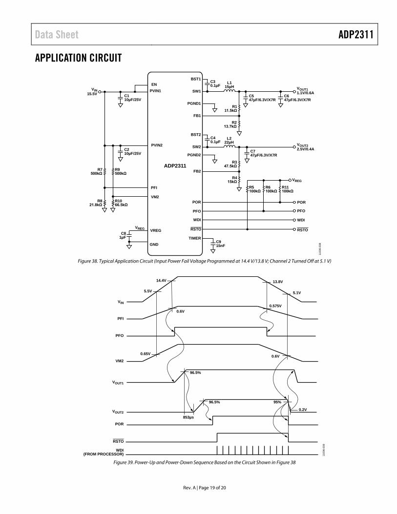
APPLICATION CIRCUIT
PVIN1EN
GND
VREG
ADP2311
BST2
SW2
FB2
C747µF/6.3V/X7RPGND2
L222µH
VM2
BST1
SW1
FB1
C547µF/6.3V/X7R
C647µF/6.3V/X7R
PGND1
PVIN2
POR
PFO PFO
POR
VREG
R11100kΩ
R6100kΩ
R5100kΩ
PFI
WDI WDI
TIMERC915nF
VREG
C30.1µF
VIN15.5V C1
10µF/25V
C81µF
C210µF/25V
R7500kΩ
R9500kΩ
R347.5kΩ
R1066.5kΩ
R821.8kΩ
L115µH
R111.5kΩ
R213.7kΩ
C40.1µF
VOUT11.1V/0.6A
VOUT22.5V/0.4A
R415kΩ
1103
6-03
8
RSTO RSTO
Figure 38. Typical Application Circuit (Input Power Fail Voltage Programmed at 14.4 V/13.8 V; Channel 2 Turned Off at 5.1 V)
14.4V
VIN
PFO
VOUT1
VOUT2
13.8V
5.1V
POR
PFI
0.6V0.575V
VM20.6V0.65V
96.5%
96.5%
5.5V
95%
0.2V
853µs
WDI(FROM PROCESSOR) 11
036-
039
RSTO
Figure 39. Power-Up and Power-Down Sequence Based on the Circuit Shown in Figure 38
ADP2311 Data Sheet
Rev. A | Page 20 of 20
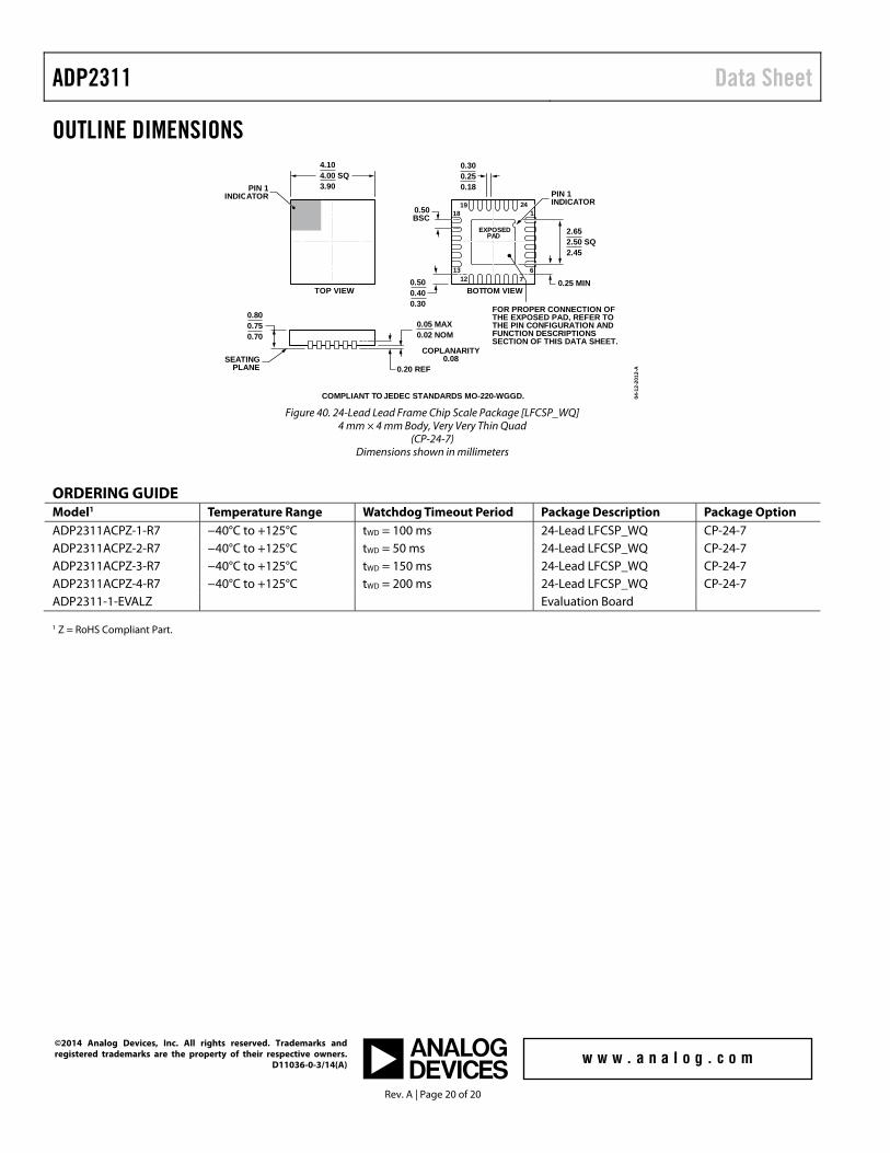
OUTLINE DIMENSIONS
0.50BSC
0.500.400.30
0.300.250.18
COMPLIANT TO JEDEC STANDARDS MO-220-WGGD. 04-1
2-20
12-A
BOTTOM VIEWTOP VIEW
EXPOSEDPAD
PIN 1INDICATOR
4.104.00 SQ3.90
SEATINGPLANE
0.800.750.70
0.20 REF
0.25 MIN
COPLANARITY0.08
PIN 1INDICATOR
2.652.50 SQ2.45
124
71213
1819
6
FOR PROPER CONNECTION OFTHE EXPOSED PAD, REFER TOTHE PIN CONFIGURATION ANDFUNCTION DESCRIPTIONSSECTION OF THIS DATA SHEET.
0.05 MAX0.02 NOM
Figure 40. 24-Lead Lead Frame Chip Scale Package [LFCSP_WQ] 4 mm × 4 mm Body, Very Very Thin Quad
(CP-24-7) Dimensions shown in millimeters
ORDERING GUIDE Model1 Temperature Range Watchdog Timeout Period Package Description Package Option ADP2311ACPZ-1-R7 −40°C to +125°C tWD = 100 ms 24-Lead LFCSP_WQ CP-24-7 ADP2311ACPZ-2-R7 −40°C to +125°C tWD = 50 ms 24-Lead LFCSP_WQ CP-24-7 ADP2311ACPZ-3-R7 −40°C to +125°C tWD = 150 ms 24-Lead LFCSP_WQ CP-24-7 ADP2311ACPZ-4-R7 −40°C to +125°C tWD = 200 ms 24-Lead LFCSP_WQ CP-24-7 ADP2311-1-EVALZ Evaluation Board
1 Z = RoHS Compliant Part.
©2014 Analog Devices, Inc. All rights reserved. Trademarks and registered trademarks are the property of their respective owners.
D11036-0-3/14(A)