Embed Size (px)
Citation preview
1FEATURES DESCRIPTION
APPLICATIONS
TPS718xx
TPS719xx
GND
EN1
EN2
OUT2
IN OUT1VIN
VOUT
VOUT
1 Fm
1 Fm
1 Fm
Typical Application Circuit
2.7V to 6.5V 0.9V to 3.6V
0.9V 3.6V-
On
Off
On
Off
EN1
GNDGND
EN2
6
5
4
OUT1
IN
OUT2
1
2
3
TPS718xx, TPS719xx
DRV Package
2mm x 2mm SON-6
(Top View)
OUT1
IN
OUT2
EN1
GND
EN2
A1
B1
C1
A2
B2
C2
TPS718Axx, TPS719Axx
YZC Package
6-BALL WCSP
(Top View)
OUT1
IN
OUT2
EN1
GND
EN2
C2
B2
A2
C1
B1
A1
TPS718xx, TPS719xx
YZC Package
6-BALL WCSP
(Top View)
TPS718xxTPS719xx
www.ti.com..................................................................................................................................................... SBVS088C–FEBRUARY 2007–REVISED MAY 2008
Dual, 200mA Output, Low Noise, High PSRRLow-Dropout Linear Regulators
23• Dual, 200mA High-Performance LDOs The TPS718xx and TPS719xx families of low-dropout(LDO) regulators offer a high power-supply rejection• Low Total Quiescent Current: 90µA with Bothratio (PSRR), low noise, fast start-up, and excellentLDOs Enabledline and load transient responses while consuming a• Low Noise: 70µVRMS/V very low 90µA (typical) at no load ground current with
• Active Output Pulldown (TPS719xx) both LDOs enabled. The TPS719xx also provides anactive pulldown circuit to quickly discharge output• Independent Enables for Each LDOloads. The TPS718xx and TPS719xx are stable with• PSRR: 65dB at 1kHz, 45dB at 1MHz ceramic capacitors and use an advanced BiCMOS
• Available in Multiple Fixed-Output Voltage fabrication process to yield a typical dropout voltageCombinations from 0.9V to 3.6V Using of 230mV at 200mA output loads. The TPS718xx andInnovative Factory EEPROM Programming TPS719xx also use a precision voltage reference and
feedback loop to achieve 3% overall accuracy over all• Fast Start-Up Time: 160µsload, line, process, and temperature variations. Both• Over-Current, Over-Temperature and families of devices are fully specified from TJ = –40°CUnder-Voltage Protection to +125°C and are offered in 2mm × 2mm SON-6 and
• Low Dropout: 230mV at 200mA 6-ball Wafer Chip-Scale (WCSP) packages that areideal for applications such as mobile handsets and• Stable with 1µF Ceramic Output CapacitorWLAN that require good thermal dissipation while• Available in 2mm × 2mm SON-6 and 6-Ball maintaining a very small footprint.WCSP Packages
• Digital Cameras and Camera Modules• Cellular Camera and TV Phones• Wireless LAN, Bluetooth®
• Handheld Products
1
Please be aware that an important notice concerning availability, standard warranty, and use in critical applications ofTexas Instruments semiconductor products and disclaimers thereto appears at the end of this data sheet.
2Bluetooth is a registered trademark of Bluetooth SIG, Inc.3All other trademarks are the property of their respective owners.
PRODUCTION DATA information is current as of publication date. Copyright © 2007–2008, Texas Instruments IncorporatedProducts conform to specifications per the terms of the TexasInstruments standard warranty. Production processing does notnecessarily include testing of all parameters.
ABSOLUTE MAXIMUM RATINGS (1)
DISSIPATION RATINGS
TPS718xxTPS719xx
SBVS088C–FEBRUARY 2007–REVISED MAY 2008..................................................................................................................................................... www.ti.com
This integrated circuit can be damaged by ESD. Texas Instruments recommends that all integrated circuits be handled withappropriate precautions. Failure to observe proper handling and installation procedures can cause damage.
ESD damage can range from subtle performance degradation to complete device failure. Precision integrated circuits may be moresusceptible to damage because very small parametric changes could cause the device not to meet its published specifications.
ORDERING INFORMATION (1)
PRODUCT VOUT(2) (3)
TPS718xx-yywwwz A denotes device with rotated pin 1 orientation of wafer-chipscale package.TPS718Axx-yywwwz XX is nominal output voltage for LDO1 (for example, 28 = 2.8V).TPS719xx-yywwwz YY is nominal output voltage for LDO2.
TPS719Axx-yywwwz WWW is package designator.Z is tape and reel quantity (R = 3000, T = 250).
Examples: TPS71918–285DRVR XX = 18 = 1.8V, YYY = 285 = 2.85VTPS719185-33DRVR XXX = 185 = 1.85V, YY = 33 = 3.3V
DRV = 2mm x 2mm SON packageZ = R = 3000 piece reel
(1) For the most current package and ordering information see the Package Option Addendum at the end of this document, or see the TIwebsite at www.ti.com.
(2) Both outputs are programmable from 0.9V to 3.6V in 50mV increments.(3) Output voltages from 0.9V to 3.6V in 50mV increments are available through the use of innovative factory EEPROM programming;
minimum order quantities may apply. Contact factory for details and availability.
Over operating temperature range (unless otherwise noted). All voltages are with respect to GND.
PARAMETER TPS718xx, TPS719xx UNITInput voltage range, VIN –0.3 to +7.0 VEnable voltage range, VEN1 and VEN2 –0.3 to VIN + 0.3V VOutput voltage range, VOUT –0.3 to +7.0 VPeak output current Internally limitedOutput short-circuit duration IndefiniteJunction temperature range, TJ –55 to +150 °CStorage temperature range , TSTG –55 to +150 °CTotal continuous power dissipation, PDISS See Dissipation Ratings TableESD rating, HBM 2 kVESD rating, CDM 500 V
(1) Stresses above these ratings may cause permanent damage. Exposure to absolute maximum conditions for extended periods maydegrade device reliability. These are stress ratings only, and functional operation of the device at these or any other conditions beyondthose specified is not implied.
DERATING FACTORBOARD PACKAGE RθJC RθJA ABOVE TA = +25°C TA < +25°C TA = +70°C TA = +85°CHigh-K (1) DRV 20°C/W 95°C/W 10.53mW/°C 1053mW 579mW 421mWHigh-K (1) YZC 27°C/W 190°C/W 5.3mW/°C 530mW 295mW 215mW
(1) The JEDEC high-K (2s2p) board used to derive this data was a 3in × 3in, multilayer board with 1-ounce internal power and groundplanes and 2-ounce copper traces on top and bottom of the board.
2 Submit Documentation Feedback Copyright © 2007–2008, Texas Instruments Incorporated
Product Folder Link(s): TPS718xx TPS719xx
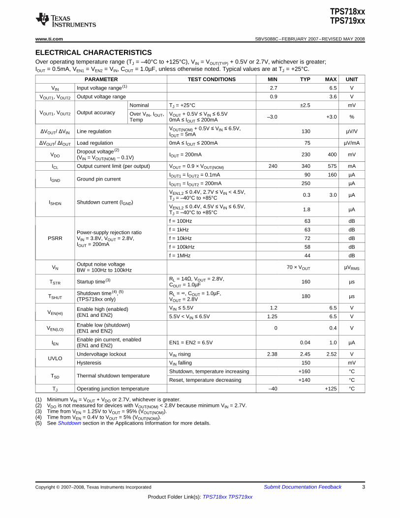
ELECTRICAL CHARACTERISTICS
TPS718xxTPS719xx
www.ti.com..................................................................................................................................................... SBVS088C–FEBRUARY 2007–REVISED MAY 2008
Over operating temperature range (TJ = –40°C to +125°C), VIN = VOUT(TYP) + 0.5V or 2.7V, whichever is greater;IOUT = 0.5mA, VEN1 = VEN2 = VIN, COUT = 1.0µF, unless otherwise noted. Typical values are at TJ = +25°C.
PARAMETER TEST CONDITIONS MIN TYP MAX UNITVIN Input voltage range (1) 2.7 6.5 V
VOUT1, VOUT2 Output voltage range 0.9 3.6 VNominal TJ = +25°C ±2.5 mV
VOUT1, VOUT2 Output accuracy Over VIN, IOUT, VOUT + 0.5V ≤ VIN ≤ 6.5V –3.0 +3.0 %Temp 0mA ≤ IOUT ≤ 200mAVOUT(NOM) + 0.5V ≤ VIN ≤ 6.5V,ΔVOUT/ ΔVIN Line regulation 130 µV/VIOUT = 5mA
ΔVOUT/ ΔIOUT Load regulation 0mA ≤ IOUT ≤ 200mA 75 µV/mADropout voltage (2)
VDO IOUT = 200mA 230 400 mV(VIN = VOUT(NOM) – 0.1V)ICL Output current limit (per output) VOUT = 0.9 × VOUT(NOM) 240 340 575 mA
IOUT1 = IOUT2 = 0.1mA 90 160 µAIGND Ground pin current
IOUT1 = IOUT2 = 200mA 250 µAVEN1,2 ≤ 0.4V, 2.7V ≤ VIN < 4.5V, 0.3 3.0 µATJ = –40°C to +85°C
ISHDN Shutdown current (IGND)VEN1,2 ≤ 0.4V, 4.5V ≤ VIN ≤ 6.5V, 1.8 µATJ = –40°C to +85°Cf = 100Hz 63 dBf = 1kHz 63 dBPower-supply rejection ratio
PSRR VIN = 3.8V, VOUT = 2.8V, f = 10kHz 72 dBIOUT = 200mA f = 100kHz 58 dB
f = 1MHz 44 dBOutput noise voltageVN 70 × VOUT µVRMSBW = 100Hz to 100kHz
RL = 14Ω, VOUT = 2.8V,TSTR Startup time (3) 160 µsCOUT = 1.0µFShutdown time (4), (5) RL = ∞, COUT = 1.0µF,TSHUT 180 µs(TPS719xx only) VOUT = 2.8V
VIN ≤ 5.5V 1.2 6.5 VEnable high (enabled)VEN(HI) (EN1 and EN2) 5.5V < VIN ≤ 6.5V 1.25 6.5 VEnable low (shutdown)VEN(LO) 0 0.4 V(EN1 and EN2)Enable pin current, enabledIEN EN1 = EN2 = 6.5V 0.04 1.0 µA(EN1 and EN2)Undervoltage lockout VIN rising 2.38 2.45 2.52 V
UVLOHysteresis VIN falling 150 mV
Shutdown, temperature increasing +160 °CTSD Thermal shutdown temperature
Reset, temperature decreasing +140 °CTJ Operating junction temperature –40 +125 °C
(1) Minimum VIN = VOUT + VDO or 2.7V, whichever is greater.(2) VDO is not measured for devices with VOUT(NOM) < 2.8V because minimum VIN = 2.7V.(3) Time from VEN = 1.25V to VOUT = 95% (VOUT(NOM)).(4) Time from VEN = 0.4V to VOUT = 5% (VOUT(NOM)).(5) See Shutdown section in the Applications Information for more details.
Copyright © 2007–2008, Texas Instruments Incorporated Submit Documentation Feedback 3
Product Folder Link(s): TPS718xx TPS719xx
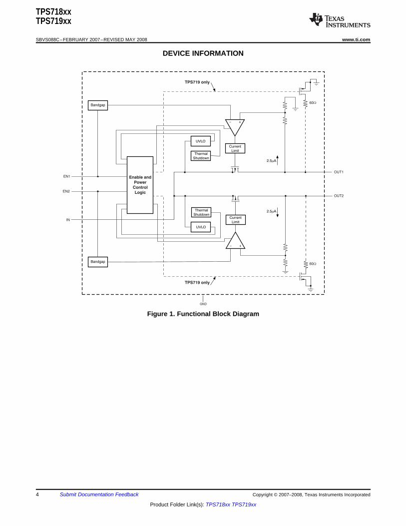
DEVICE INFORMATION
GND
Bandgap
Bandgap
2.5 Am
2.5 Am
Current
LimitThermal
Shutdown
UVLO
Current
Limit
Thermal
Shutdown
UVLO
Enable and
Power
Control
Logic
60W
60W
OUT1
OUT2
EN1
EN2
IN
TPS719 only
TPS719 only
TPS718xxTPS719xx
SBVS088C–FEBRUARY 2007–REVISED MAY 2008..................................................................................................................................................... www.ti.com
Figure 1. Functional Block Diagram
4 Submit Documentation Feedback Copyright © 2007–2008, Texas Instruments Incorporated
Product Folder Link(s): TPS718xx TPS719xx
EN1
GNDGND
EN2
6
5
4
OUT1
IN
OUT2
1
2
3
OUT1
IN
OUT2
EN1
GND
EN2
C2
B2
A2
C1
B1
A1
TPS718xx
TPS719xx
TPS718Axx
TPS719Axx
OUT1
IN
OUT2
EN1
GND
EN2
A1
B1
C1
A2
B2
C2
TPS718xxTPS719xx
www.ti.com..................................................................................................................................................... SBVS088C–FEBRUARY 2007–REVISED MAY 2008
DRV PACKAGESON-6
(TOP VIEW)
YZC PACKAGE6-BALL WCSP
(TOP VIEW)
YZC PACKAGE6-BALL WCSP
(TOP VIEW)
PIN DESCRIPTIONSTPS718xx TPS718Axx (1)
TPS719xx TPS719Axx (1)
NAME DRV YZC YZC DESCRIPTIONOutput of Regulator 1. A small ceramic capacitor (typically ≥ 1µF) isOUT1 1 C1 A2 needed from this pin to ground to assure stability.
IN 2 B1 B2 Input supply to both regulators.Output of Regulator 2. A small ceramic capacitor (typically ≥ 1µF) isOUT2 3 A1 C2 needed from this pin to ground to assure stability.Enable pin for Regulator 2. Driving the Enable pin (EN2) high turns on
EN2 4 A2 C1 Regulator 2. Driving this pin low puts Regulator 2 into shutdown mode,reducing operating current.
GND 5 B2 B1 Ground. DRV thermal pad should also be connected to ground.Enable pin for Regulator 1. Driving the Enable pin (EN1) high turns on
EN1 6 C2 A1 Regulator 1. Driving this pin low puts Regulator 1 into shutdown mode,reducing operating current.
(1) A option denotes devices with rotated Pin 1 orientation on Wafer Chipscale packages.
Copyright © 2007–2008, Texas Instruments Incorporated Submit Documentation Feedback 5
Product Folder Link(s): TPS718xx TPS719xx
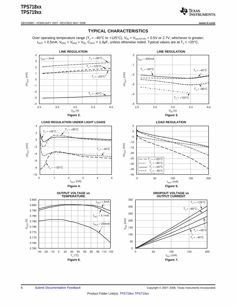
TYPICAL CHARACTERISTICS
4
3
2
1
0
1
2
3
4
-
-
-
-
DV
(mV
)O
UT
2.5 5.5 6.5
V (V)IN
3.5 4.5
I = 5mAOUT
T = +25 CJ °
T = +85 CJ °
T = +125 CJ °
T = 0 CJ -4 °
0
1
2
3
4
5
-
-
-
-
-
DV
(mV
)O
UT
T = +85 CJ °
T = +125 CJ °
T = +25 CJ ° T = 40 CJ - °
I = 200mAOUT
2.5 5.5 6.5
V (V)IN
3.5 4.5
4
2
0
2
4
6
8
10
-
-
-
-
-
I (mA)OUT
DV
(mV
)O
UT
0 51 2 3 4
T = +85 CJ °
T = +125 CJ °
T = +25 CJ °
T = 40 CJ - °
5
0
5
10
15
20
25
30
35
40
-
-
-
-
-
-
-
-
0 50 100 150 200
I (mA)OUT
DV
(mV
)O
UT
T = +125 CJ
T = +85 C
T = +25 C
T = 40 C
J
J
J -
°
°
°
°
2.805
2.800
2.795
2.790
2.785
2.780
2.775
2.770
2.765
2.760
V(V
)O
UT
-40 65 125
T ( C)J °
5 35-25 -10 20 50 80 95 110
I = 5mAOUT
I = 0.1mAOUT
I = 200mAOUT
350
300
250
200
150
100
50
0
0 100 200
I (mA)OUT
V(m
V)
DO
50 150
T = +125 CJ °
T = +85 CJ °
T = +25 CJ °
T = 40 C-J °
TPS718xxTPS719xx
SBVS088C–FEBRUARY 2007–REVISED MAY 2008..................................................................................................................................................... www.ti.com
Over operating temperature range (TJ = –40°C to +125°C), VIN = VOUT(TYP) + 0.5V or 2.7V, whichever is greater;IOUT = 0.5mA, VEN1 = VEN2 = VIN, COUT = 1.0µF, unless otherwise noted. Typical values are at TJ = +25°C.
LINE REGULATION LINE REGULATION
Figure 2. Figure 3.
LOAD REGULATION UNDER LIGHT LOADS LOAD REGULATION
Figure 4. Figure 5.
OUTPUT VOLTAGE vs DROPOUT VOLTAGE vsTEMPERATURE OUTPUT CURRENT
Figure 6. Figure 7.
6 Submit Documentation Feedback Copyright © 2007–2008, Texas Instruments Incorporated
Product Folder Link(s): TPS718xx TPS719xx
200
160
120
80
40
0
0 100 200
I (mA)OUT
I(
A)
mG
ND
50 150
T = +125 CJ °
T = 0 CJ -4 °
T = +85 CJ °
T = +25 CJ °
60
50
40
30
20
10
0
I(
A)
mG
ND
2.5 5.5 6.5
V (V)IN
3.5 4.5
I = 1mAOUT
-40 65 125
T ( C)J °
5 35-25 -10 20 50 80 95 110
140
120
100
80
60
40
20
0
I(
A)
mG
ND
I = 0mAOUT
5.0
4.5
4.0
3.5
3.0
2.5
2.0
1.5
1.0
0.5
0
Shutd
ow
n C
urr
ent (
A)
m
T = 40 CJ - °
2.5 5.5 6.5
V (V)IN
3.5 4.5
T = +125 CJ °
T = +85 CJ °
T = +25 CJ °
450
425
400
375
350
325
300
275
250
Curr
ent Lim
it (
mA
)
2.5 5.5 6.5
V (V)IN
3.5 4.5
T = +125 CJ
T = +85 C
T = +25 C
T = 40 C
J
J
J -
°
°
°
°
90
80
70
60
50
40
30
20
10
0
PS
RR
(dB
)
10 100k 10M
Frequency (Hz)
1k 10k100 1M
5mA
100mA
200mA
TPS718xxTPS719xx
www.ti.com..................................................................................................................................................... SBVS088C–FEBRUARY 2007–REVISED MAY 2008
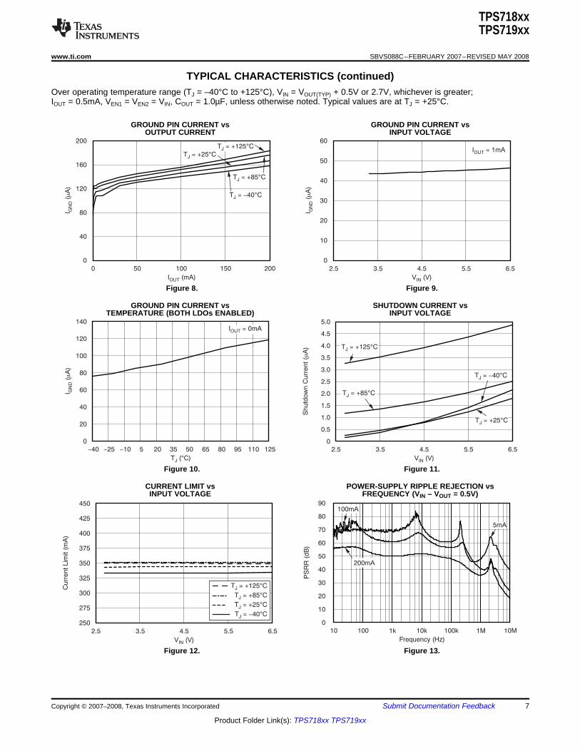
TYPICAL CHARACTERISTICS (continued)Over operating temperature range (TJ = –40°C to +125°C), VIN = VOUT(TYP) + 0.5V or 2.7V, whichever is greater;IOUT = 0.5mA, VEN1 = VEN2 = VIN, COUT = 1.0µF, unless otherwise noted. Typical values are at TJ = +25°C.
GROUND PIN CURRENT vs GROUND PIN CURRENT vsOUTPUT CURRENT INPUT VOLTAGE
Figure 8. Figure 9.
GROUND PIN CURRENT vs SHUTDOWN CURRENT vsTEMPERATURE (BOTH LDOs ENABLED) INPUT VOLTAGE
Figure 10. Figure 11.
CURRENT LIMIT vs POWER-SUPPLY RIPPLE REJECTION vsINPUT VOLTAGE FREQUENCY (VIN – VOUT = 0.5V)
Figure 12. Figure 13.
Copyright © 2007–2008, Texas Instruments Incorporated Submit Documentation Feedback 7
Product Folder Link(s): TPS718xx TPS719xx
80
70
60
50
40
30
20
10
0
V (V)IN
PS
RR
(dB
)
3.0 4.03.2 3.4 3.6 3.8
V = 2.80VOUT
I = 5mAOUT
10kHz
1kHz
100kHz
1MHz
90
80
70
60
50
40
30
20
10
0
PS
RR
(dB
)
10 100k 10M
Frequency (Hz)
1k 10k100 1M
5mA
100mA
200mA
80
70
60
50
40
30
20
10
0
V (V)IN
PS
RR
(dB
)
3.0 4.03.2 3.4 3.6 3.8
V = 2.80V
I = 200mAOUT
OUT
10kHz
1kHz
100kHz
1MHz
10
1
0.1
0.01
Outp
ut S
pectr
al N
ois
e D
ensity (
V)
mH
zÖ
100 10k 100k
Frequency (Hz)
1k
V = 2.80VOUT
10 s/divm
3.3V
6.5V
1V/div
10mV/div
10mV/div
VIN
VOUT1
VOUT2
= 1V/ smdVIN
dt
20 s/divm
IOUT1
VOUT1
VOUT2
250mA/div
10mV/div
10mV/div
= 200mA/ smdIOUT
dt
I = 3mAOUTmin
TPS718xxTPS719xx
SBVS088C–FEBRUARY 2007–REVISED MAY 2008..................................................................................................................................................... www.ti.com
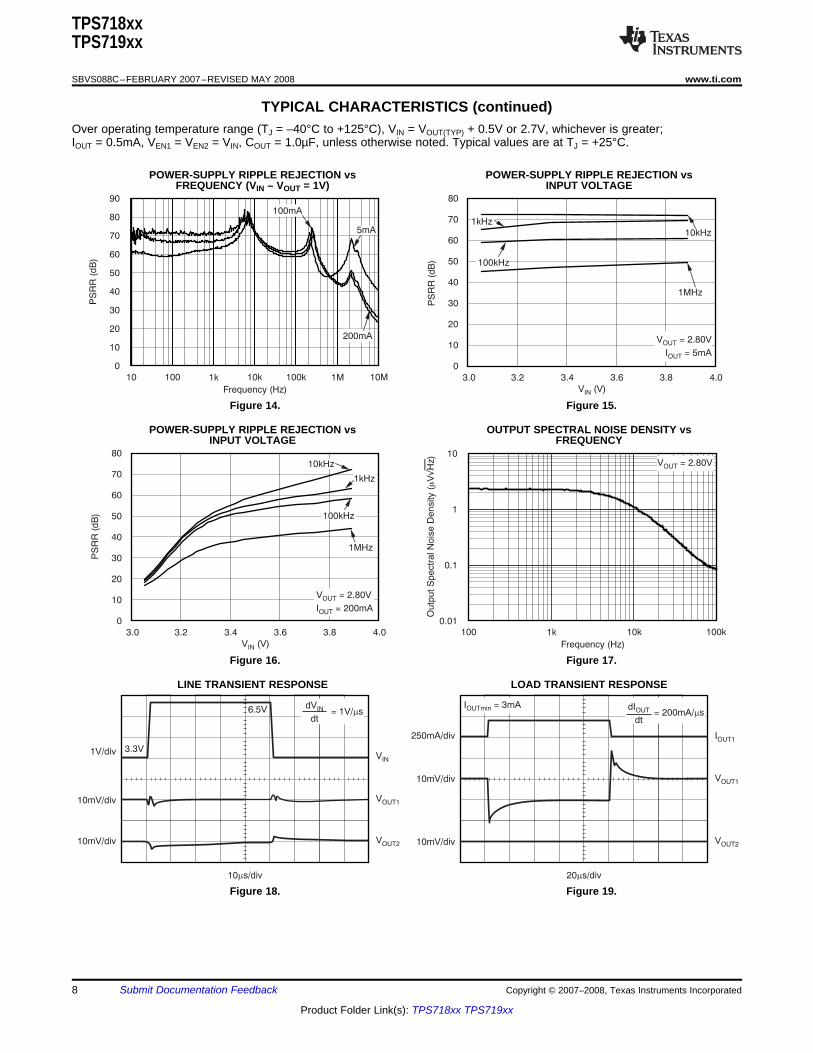
TYPICAL CHARACTERISTICS (continued)Over operating temperature range (TJ = –40°C to +125°C), VIN = VOUT(TYP) + 0.5V or 2.7V, whichever is greater;IOUT = 0.5mA, VEN1 = VEN2 = VIN, COUT = 1.0µF, unless otherwise noted. Typical values are at TJ = +25°C.
POWER-SUPPLY RIPPLE REJECTION vs POWER-SUPPLY RIPPLE REJECTION vsFREQUENCY (VIN – VOUT = 1V) INPUT VOLTAGE
Figure 14. Figure 15.
POWER-SUPPLY RIPPLE REJECTION vs OUTPUT SPECTRAL NOISE DENSITY vsINPUT VOLTAGE FREQUENCY
Figure 16. Figure 17.
LINE TRANSIENT RESPONSE LOAD TRANSIENT RESPONSE
Figure 18. Figure 19.
8 Submit Documentation Feedback Copyright © 2007–2008, Texas Instruments Incorporated
Product Folder Link(s): TPS718xx TPS719xx
40 s/divm
0V
6.5V
4V/div
1V/div
1V/div
EN1, EN2
VOUT1
VOUT2
VINIOUT = 200mA
VOUT1V/div
400ms/div
TPS718xxTPS719xx
www.ti.com..................................................................................................................................................... SBVS088C–FEBRUARY 2007–REVISED MAY 2008
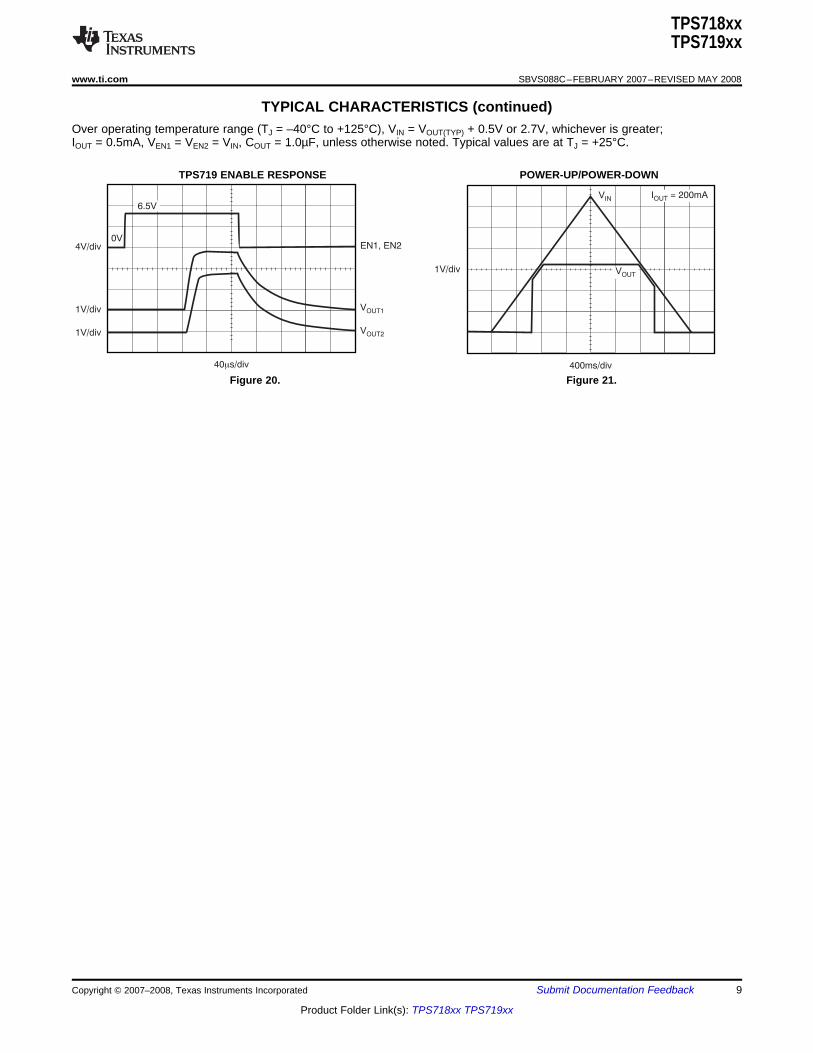
TYPICAL CHARACTERISTICS (continued)Over operating temperature range (TJ = –40°C to +125°C), VIN = VOUT(TYP) + 0.5V or 2.7V, whichever is greater;IOUT = 0.5mA, VEN1 = VEN2 = VIN, COUT = 1.0µF, unless otherwise noted. Typical values are at TJ = +25°C.
TPS719 ENABLE RESPONSE POWER-UP/POWER-DOWN
Figure 20. Figure 21.
Copyright © 2007–2008, Texas Instruments Incorporated Submit Documentation Feedback 9
Product Folder Link(s): TPS718xx TPS719xx
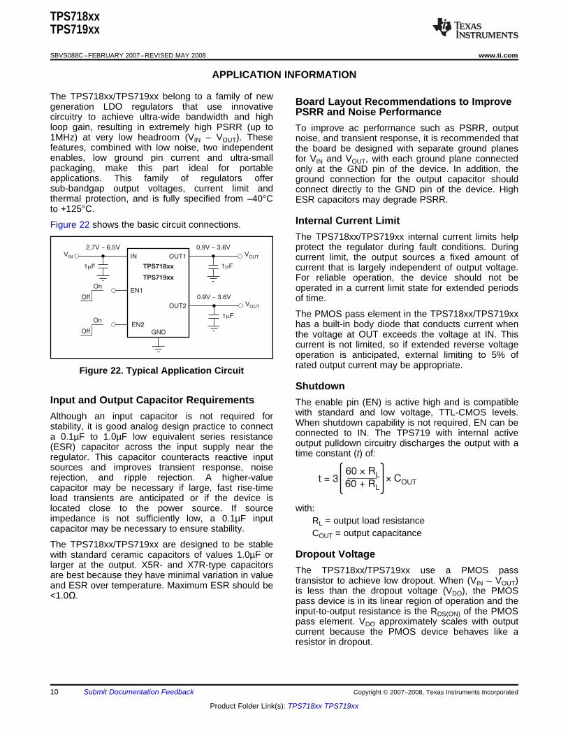
APPLICATION INFORMATION
Board Layout Recommendations to Improve
Internal Current Limit
TPS718xx
TPS719xx
GND
EN1
EN2
OUT2
IN OUT1VIN
VOUT
VOUT
1 Fm
1 Fm
1 Fm
2.7V 6.5V- 0.9V 3.6V-
0.9V 3.6V-
On
Off
On
Off
ShutdownInput and Output Capacitor Requirements
t = 360 R
L´
60 + RL
COUT
´
Dropout Voltage
TPS718xxTPS719xx
SBVS088C–FEBRUARY 2007–REVISED MAY 2008..................................................................................................................................................... www.ti.com
The TPS718xx/TPS719xx belong to a family of newgeneration LDO regulators that use innovative PSRR and Noise Performancecircuitry to achieve ultra-wide bandwidth and highloop gain, resulting in extremely high PSRR (up to To improve ac performance such as PSRR, output1MHz) at very low headroom (VIN – VOUT). These noise, and transient response, it is recommended thatfeatures, combined with low noise, two independent the board be designed with separate ground planesenables, low ground pin current and ultra-small for VIN and VOUT, with each ground plane connectedpackaging, make this part ideal for portable only at the GND pin of the device. In addition, theapplications. This family of regulators offer ground connection for the output capacitor shouldsub-bandgap output voltages, current limit and connect directly to the GND pin of the device. Highthermal protection, and is fully specified from –40°C ESR capacitors may degrade PSRR.to +125°C.
Figure 22 shows the basic circuit connections.The TPS718xx/TPS719xx internal current limits helpprotect the regulator during fault conditions. Duringcurrent limit, the output sources a fixed amount ofcurrent that is largely independent of output voltage.For reliable operation, the device should not beoperated in a current limit state for extended periodsof time.
The PMOS pass element in the TPS718xx/TPS719xxhas a built-in body diode that conducts current whenthe voltage at OUT exceeds the voltage at IN. Thiscurrent is not limited, so if extended reverse voltageoperation is anticipated, external limiting to 5% ofrated output current may be appropriate.Figure 22. Typical Application Circuit
The enable pin (EN) is active high and is compatiblewith standard and low voltage, TTL-CMOS levels.Although an input capacitor is not required forWhen shutdown capability is not required, EN can bestability, it is good analog design practice to connectconnected to IN. The TPS719 with internal activea 0.1µF to 1.0µF low equivalent series resistanceoutput pulldown circuitry discharges the output with a(ESR) capacitor across the input supply near thetime constant (t) of:regulator. This capacitor counteracts reactive input
sources and improves transient response, noiserejection, and ripple rejection. A higher-valuecapacitor may be necessary if large, fast rise-timeload transients are anticipated or if the device islocated close to the power source. If source with:impedance is not sufficiently low, a 0.1µF input RL = output load resistancecapacitor may be necessary to ensure stability. COUT = output capacitanceThe TPS718xx/TPS719xx are designed to be stablewith standard ceramic capacitors of values 1.0µF orlarger at the output. X5R- and X7R-type capacitors The TPS718xx/TPS719xx use a PMOS passare best because they have minimal variation in value transistor to achieve low dropout. When (VIN – VOUT)and ESR over temperature. Maximum ESR should be is less than the dropout voltage (VDO), the PMOS<1.0Ω. pass device is in its linear region of operation and the
input-to-output resistance is the RDS(ON) of the PMOSpass element. VDO approximately scales with outputcurrent because the PMOS device behaves like aresistor in dropout.
10 Submit Documentation Feedback Copyright © 2007–2008, Texas Instruments Incorporated
Product Folder Link(s): TPS718xx TPS719xx
Transient Response
Undervoltage Lock-Out (UVLO)
Power Dissipation
Minimum Load
THERMAL INFORMATION
Thermal Protection
P = (V V ) x I-D IN OUT OUT (1)
Package Mounting
TPS718xxTPS719xx
www.ti.com..................................................................................................................................................... SBVS088C–FEBRUARY 2007–REVISED MAY 2008
As with any linear regulator, PSRR and transient Any tendency to activate the thermal protection circuitresponse are degraded as (VIN – VOUT) approaches indicates excessive power dissipation or andropout. This effect is shown in Figure 13 and inadequate heatsink. For reliable operation, junctionFigure 14 in the Typical Characteristics section. temperature should be limited to +125°C maximum.
To estimate the margin of safety in a complete design(including heatsink), increase the ambienttemperature until the thermal protection is triggered;
As with any regulator, increasing the size of the use worst-case loads and signal conditions. For goodoutput capacitor will reduce over/undershoot reliability, thermal protection should trigger at leastmagnitude but increase duration of the transient +35°C above the maximum expected ambientresponse. condition of your particular application. This
configuration produces a worst-case junctiontemperature of +125°C at the highest expectedambient temperature and worst-case load.The TPS718xx/TPS719xx utilize an undervoltage
lock-out circuit to keep the output shut off until The internal protection circuitry of theinternal circuitry is operating properly. The UVLO TPS718xx/TPS719xx has been designed to protectcircuit has a de-glitch feature so that it typically against overload conditions. It was not intended toignores undershoot transients on the input if they are replace proper heatsinking. Continuously running theless than 50µs duration. On the TPS719xx, the active TPS718xx/TPS719xx into thermal shutdownpulldown discharges VOUT when the device is in degrades device reliability.UVLO off condition. However, the input voltage needsto be greater than 0.8V for active pulldown to work.
The ability to remove heat from the die is different foreach package type, presenting different
The TPS718xx/TPS719xx are stable with no output considerations in the printed circuit board (PCB)load. Traditional PMOS LDO regulators suffer from layout. The PCB area around the device that is freelower loop gain at very light output loads. The of other components moves the heat from the deviceTPS718xx/TPS719xx employ an innovative, to the ambient air. Performance data for JEDEC low-low-current mode circuit under very light or no-load and high-K boards are given in the Dissipationconditions, resulting in improved output voltage Ratings table. Using heavier copper increases theregulation performance down to zero output current. effectiveness in removing heat from the device. The
addition of plated through-holes to heat-dissipatinglayers also improves the heatsink effectiveness.
Power dissipation depends on input voltage and loadconditions. Power dissipation (PD) is equal to the
Thermal protection disables the output when the product of the output current times the voltage dropjunction temperature rises to approximately +160°C, across the output pass element (VIN to VOUT), asallowing the device to cool. When the junction shown in Equation 1:temperature cools to approximately +140°C theoutput circuitry is again enabled. Depending on powerdissipation, thermal resistance, and ambienttemperature, the thermal protection circuit may cycleon and off. This cycling limits the dissipation of the Solder pad footprint recommendations for theregulator, protecting it from damage due to TPS718xx/TPS719xxx are available from the Texasoverheating. Instruments web site at www.ti.com.
Copyright © 2007–2008, Texas Instruments Incorporated Submit Documentation Feedback 11
Product Folder Link(s): TPS718xx TPS719xx

1,690
1,590
1,088
0,988
TPS718xxTPS719xx
SBVS088C–FEBRUARY 2007–REVISED MAY 2008..................................................................................................................................................... www.ti.com
Figure 23. YZC Wafer Chip-Scale Package Dimensions (in mm)
12 Submit Documentation Feedback Copyright © 2007–2008, Texas Instruments Incorporated
Product Folder Link(s): TPS718xx TPS719xx
PACKAGE OPTION ADDENDUM
www.ti.com 20-Dec-2017
Addendum-Page 1
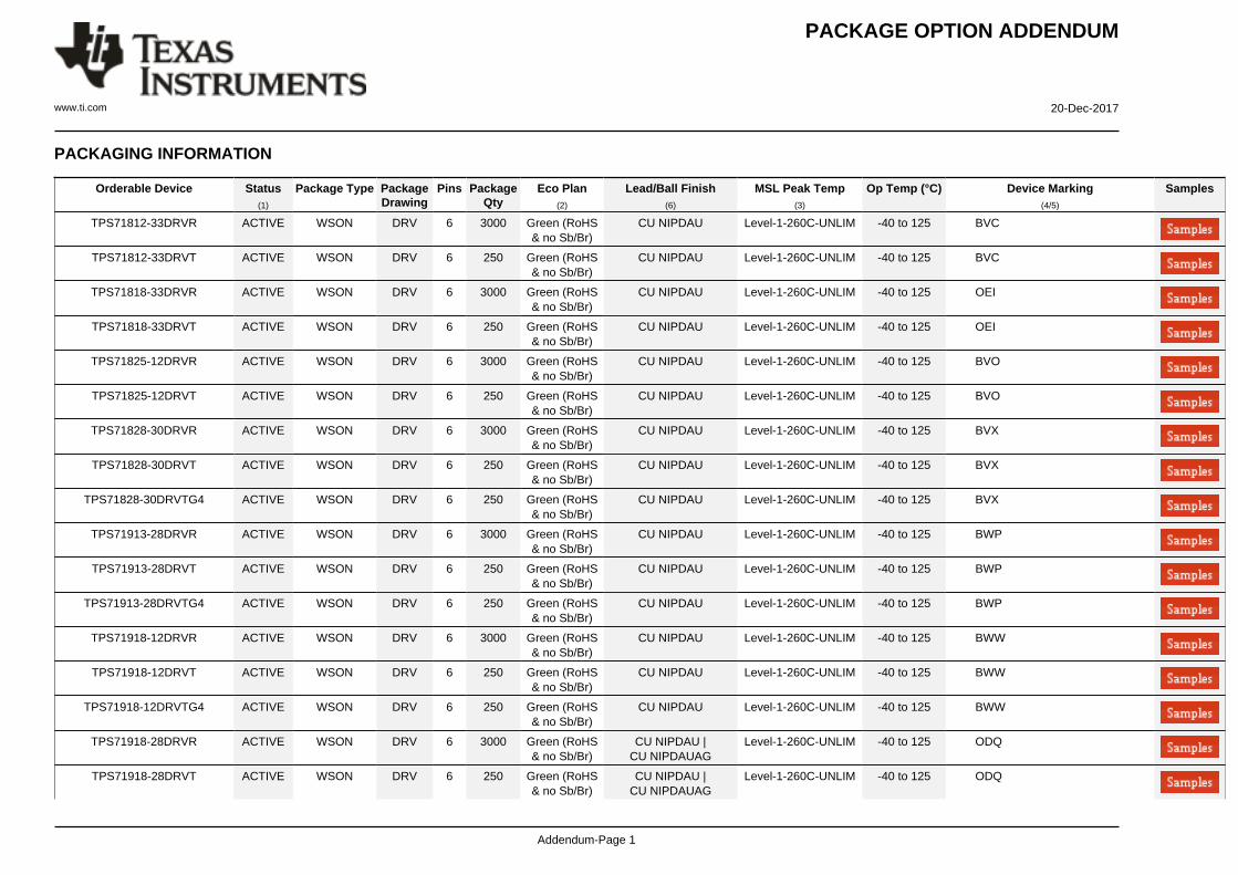
PACKAGING INFORMATION
Orderable Device Status(1)
Package Type PackageDrawing
Pins PackageQty
Eco Plan(2)
Lead/Ball Finish(6)
MSL Peak Temp(3)
Op Temp (°C) Device Marking(4/5)
Samples
TPS71812-33DRVR ACTIVE WSON DRV 6 3000 Green (RoHS& no Sb/Br)
CU NIPDAU Level-1-260C-UNLIM -40 to 125 BVC
TPS71812-33DRVT ACTIVE WSON DRV 6 250 Green (RoHS& no Sb/Br)
CU NIPDAU Level-1-260C-UNLIM -40 to 125 BVC
TPS71818-33DRVR ACTIVE WSON DRV 6 3000 Green (RoHS& no Sb/Br)
CU NIPDAU Level-1-260C-UNLIM -40 to 125 OEI
TPS71818-33DRVT ACTIVE WSON DRV 6 250 Green (RoHS& no Sb/Br)
CU NIPDAU Level-1-260C-UNLIM -40 to 125 OEI
TPS71825-12DRVR ACTIVE WSON DRV 6 3000 Green (RoHS& no Sb/Br)
CU NIPDAU Level-1-260C-UNLIM -40 to 125 BVO
TPS71825-12DRVT ACTIVE WSON DRV 6 250 Green (RoHS& no Sb/Br)
CU NIPDAU Level-1-260C-UNLIM -40 to 125 BVO
TPS71828-30DRVR ACTIVE WSON DRV 6 3000 Green (RoHS& no Sb/Br)
CU NIPDAU Level-1-260C-UNLIM -40 to 125 BVX
TPS71828-30DRVT ACTIVE WSON DRV 6 250 Green (RoHS& no Sb/Br)
CU NIPDAU Level-1-260C-UNLIM -40 to 125 BVX
TPS71828-30DRVTG4 ACTIVE WSON DRV 6 250 Green (RoHS& no Sb/Br)
CU NIPDAU Level-1-260C-UNLIM -40 to 125 BVX
TPS71913-28DRVR ACTIVE WSON DRV 6 3000 Green (RoHS& no Sb/Br)
CU NIPDAU Level-1-260C-UNLIM -40 to 125 BWP
TPS71913-28DRVT ACTIVE WSON DRV 6 250 Green (RoHS& no Sb/Br)
CU NIPDAU Level-1-260C-UNLIM -40 to 125 BWP
TPS71913-28DRVTG4 ACTIVE WSON DRV 6 250 Green (RoHS& no Sb/Br)
CU NIPDAU Level-1-260C-UNLIM -40 to 125 BWP
TPS71918-12DRVR ACTIVE WSON DRV 6 3000 Green (RoHS& no Sb/Br)
CU NIPDAU Level-1-260C-UNLIM -40 to 125 BWW
TPS71918-12DRVT ACTIVE WSON DRV 6 250 Green (RoHS& no Sb/Br)
CU NIPDAU Level-1-260C-UNLIM -40 to 125 BWW
TPS71918-12DRVTG4 ACTIVE WSON DRV 6 250 Green (RoHS& no Sb/Br)
CU NIPDAU Level-1-260C-UNLIM -40 to 125 BWW
TPS71918-28DRVR ACTIVE WSON DRV 6 3000 Green (RoHS& no Sb/Br)
CU NIPDAU |CU NIPDAUAG
Level-1-260C-UNLIM -40 to 125 ODQ
TPS71918-28DRVT ACTIVE WSON DRV 6 250 Green (RoHS& no Sb/Br)
CU NIPDAU |CU NIPDAUAG
Level-1-260C-UNLIM -40 to 125 ODQ

PACKAGE OPTION ADDENDUM
www.ti.com 20-Dec-2017
Addendum-Page 2
Orderable Device Status(1)
Package Type PackageDrawing
Pins PackageQty
Eco Plan(2)
Lead/Ball Finish(6)
MSL Peak Temp(3)
Op Temp (°C) Device Marking(4/5)
Samples
TPS71921-22DRVR ACTIVE WSON DRV 6 3000 Green (RoHS& no Sb/Br)
CU NIPDAU Level-1-260C-UNLIM -40 to 125 OBW
TPS71921-22DRVT ACTIVE WSON DRV 6 250 Green (RoHS& no Sb/Br)
CU NIPDAU Level-1-260C-UNLIM -40 to 125 OBW
TPS71926-15DRVR ACTIVE WSON DRV 6 3000 Green (RoHS& no Sb/Br)
CU NIPDAU Level-1-260C-UNLIM -40 to 125 CAJ
TPS71926-15DRVT ACTIVE WSON DRV 6 250 Green (RoHS& no Sb/Br)
CU NIPDAU Level-1-260C-UNLIM -40 to 125 CAJ
TPS71926-15DRVTG4 ACTIVE WSON DRV 6 250 Green (RoHS& no Sb/Br)
CU NIPDAU Level-1-260C-UNLIM -40 to 125 CAJ
TPS71928-28DRVR ACTIVE WSON DRV 6 3000 Green (RoHS& no Sb/Br)
CU NIPDAU Level-1-260C-UNLIM -40 to 125 CAK
TPS71928-28DRVT ACTIVE WSON DRV 6 250 Green (RoHS& no Sb/Br)
CU NIPDAU Level-1-260C-UNLIM -40 to 125 CAK
TPS71928-28DRVTG4 ACTIVE WSON DRV 6 250 Green (RoHS& no Sb/Br)
CU NIPDAU Level-1-260C-UNLIM -40 to 125 CAK
TPS719285-285DRVR ACTIVE WSON DRV 6 3000 Green (RoHS& no Sb/Br)
CU NIPDAU Level-1-260C-UNLIM -40 to 125 OAU
TPS71933-28DRVR ACTIVE WSON DRV 6 3000 Green (RoHS& no Sb/Br)
CU NIPDAU Level-1-260C-UNLIM -40 to 125 CAH
TPS71933-28DRVRG4 ACTIVE WSON DRV 6 3000 Green (RoHS& no Sb/Br)
CU NIPDAU Level-1-260C-UNLIM -40 to 125 CAH
TPS71933-28DRVT ACTIVE WSON DRV 6 250 Green (RoHS& no Sb/Br)
CU NIPDAU Level-1-260C-UNLIM -40 to 125 CAH
TPS71933-28DRVTG4 ACTIVE WSON DRV 6 250 Green (RoHS& no Sb/Br)
CU NIPDAU Level-1-260C-UNLIM -40 to 125 CAH
TPS71933-33DRVR ACTIVE WSON DRV 6 3000 Green (RoHS& no Sb/Br)
CU NIPDAU Level-1-260C-UNLIM -40 to 125 BWL
TPS71933-33DRVT ACTIVE WSON DRV 6 250 Green (RoHS& no Sb/Br)
CU NIPDAU Level-1-260C-UNLIM -40 to 125 BWL
TPS71933-33DRVTG4 ACTIVE WSON DRV 6 250 Green (RoHS& no Sb/Br)
CU NIPDAU Level-1-260C-UNLIM -40 to 125 BWL
TPS71936-315DRVR ACTIVE WSON DRV 6 3000 Green (RoHS& no Sb/Br)
CU NIPDAU Level-1-260C-UNLIM -40 to 125 CVZ
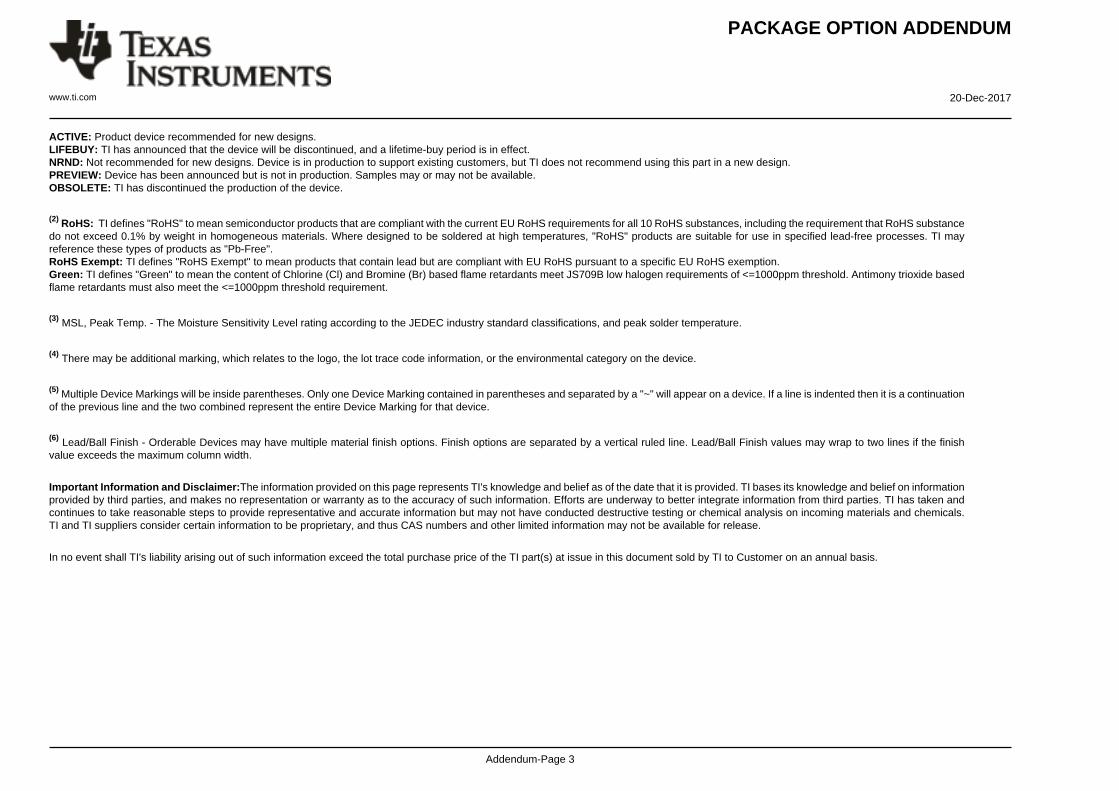
(1) The marketing status values are defined as follows:
PACKAGE OPTION ADDENDUM
www.ti.com 20-Dec-2017
Addendum-Page 3
ACTIVE: Product device recommended for new designs.LIFEBUY: TI has announced that the device will be discontinued, and a lifetime-buy period is in effect.NRND: Not recommended for new designs. Device is in production to support existing customers, but TI does not recommend using this part in a new design.PREVIEW: Device has been announced but is not in production. Samples may or may not be available.OBSOLETE: TI has discontinued the production of the device.
(2) RoHS: TI defines "RoHS" to mean semiconductor products that are compliant with the current EU RoHS requirements for all 10 RoHS substances, including the requirement that RoHS substancedo not exceed 0.1% by weight in homogeneous materials. Where designed to be soldered at high temperatures, "RoHS" products are suitable for use in specified lead-free processes. TI mayreference these types of products as "Pb-Free".RoHS Exempt: TI defines "RoHS Exempt" to mean products that contain lead but are compliant with EU RoHS pursuant to a specific EU RoHS exemption.Green: TI defines "Green" to mean the content of Chlorine (Cl) and Bromine (Br) based flame retardants meet JS709B low halogen requirements of <=1000ppm threshold. Antimony trioxide basedflame retardants must also meet the <=1000ppm threshold requirement.
(3) MSL, Peak Temp. - The Moisture Sensitivity Level rating according to the JEDEC industry standard classifications, and peak solder temperature.
(4) There may be additional marking, which relates to the logo, the lot trace code information, or the environmental category on the device.
(5) Multiple Device Markings will be inside parentheses. Only one Device Marking contained in parentheses and separated by a "~" will appear on a device. If a line is indented then it is a continuationof the previous line and the two combined represent the entire Device Marking for that device.
(6) Lead/Ball Finish - Orderable Devices may have multiple material finish options. Finish options are separated by a vertical ruled line. Lead/Ball Finish values may wrap to two lines if the finishvalue exceeds the maximum column width.
Important Information and Disclaimer:The information provided on this page represents TI's knowledge and belief as of the date that it is provided. TI bases its knowledge and belief on informationprovided by third parties, and makes no representation or warranty as to the accuracy of such information. Efforts are underway to better integrate information from third parties. TI has taken andcontinues to take reasonable steps to provide representative and accurate information but may not have conducted destructive testing or chemical analysis on incoming materials and chemicals.TI and TI suppliers consider certain information to be proprietary, and thus CAS numbers and other limited information may not be available for release.
In no event shall TI's liability arising out of such information exceed the total purchase price of the TI part(s) at issue in this document sold by TI to Customer on an annual basis.

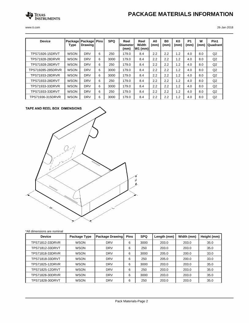
TAPE AND REEL INFORMATION
*All dimensions are nominal
Device PackageType
PackageDrawing
Pins SPQ ReelDiameter
(mm)
ReelWidth
W1 (mm)
A0(mm)
B0(mm)
K0(mm)
P1(mm)
W(mm)
Pin1Quadrant
TPS71812-33DRVR WSON DRV 6 3000 179.0 8.4 2.2 2.2 1.2 4.0 8.0 Q2
TPS71812-33DRVT WSON DRV 6 250 179.0 8.4 2.2 2.2 1.2 4.0 8.0 Q2
TPS71818-33DRVR WSON DRV 6 3000 178.0 8.4 2.25 2.25 1.0 4.0 8.0 Q2
TPS71818-33DRVT WSON DRV 6 250 178.0 8.4 2.25 2.25 1.0 4.0 8.0 Q2
TPS71825-12DRVR WSON DRV 6 3000 179.0 8.4 2.2 2.2 1.2 4.0 8.0 Q2
TPS71825-12DRVT WSON DRV 6 250 179.0 8.4 2.2 2.2 1.2 4.0 8.0 Q2
TPS71828-30DRVR WSON DRV 6 3000 179.0 8.4 2.2 2.2 1.2 4.0 8.0 Q2
TPS71828-30DRVT WSON DRV 6 250 179.0 8.4 2.2 2.2 1.2 4.0 8.0 Q2
TPS71913-28DRVR WSON DRV 6 3000 179.0 8.4 2.2 2.2 1.2 4.0 8.0 Q2
TPS71913-28DRVT WSON DRV 6 250 179.0 8.4 2.2 2.2 1.2 4.0 8.0 Q2
TPS71918-12DRVR WSON DRV 6 3000 179.0 8.4 2.2 2.2 1.2 4.0 8.0 Q2
TPS71918-12DRVT WSON DRV 6 250 179.0 8.4 2.2 2.2 1.2 4.0 8.0 Q2
TPS71918-28DRVR WSON DRV 6 3000 178.0 8.4 2.25 2.25 1.0 4.0 8.0 Q2
TPS71918-28DRVR WSON DRV 6 3000 179.0 8.4 2.2 2.2 1.2 4.0 8.0 Q2
TPS71918-28DRVT WSON DRV 6 250 178.0 8.4 2.25 2.25 1.0 4.0 8.0 Q2
TPS71921-22DRVR WSON DRV 6 3000 179.0 8.4 2.2 2.2 1.2 4.0 8.0 Q2
TPS71921-22DRVT WSON DRV 6 250 179.0 8.4 2.2 2.2 1.2 4.0 8.0 Q2
TPS71926-15DRVR WSON DRV 6 3000 179.0 8.4 2.2 2.2 1.2 4.0 8.0 Q2
PACKAGE MATERIALS INFORMATION
www.ti.com 26-Jan-2018
Pack Materials-Page 1
Device PackageType
PackageDrawing
Pins SPQ ReelDiameter
(mm)
ReelWidth
W1 (mm)
A0(mm)
B0(mm)
K0(mm)
P1(mm)
W(mm)
Pin1Quadrant
TPS71926-15DRVT WSON DRV 6 250 179.0 8.4 2.2 2.2 1.2 4.0 8.0 Q2
TPS71928-28DRVR WSON DRV 6 3000 179.0 8.4 2.2 2.2 1.2 4.0 8.0 Q2
TPS71928-28DRVT WSON DRV 6 250 179.0 8.4 2.2 2.2 1.2 4.0 8.0 Q2
TPS719285-285DRVR WSON DRV 6 3000 179.0 8.4 2.2 2.2 1.2 4.0 8.0 Q2
TPS71933-28DRVR WSON DRV 6 3000 179.0 8.4 2.2 2.2 1.2 4.0 8.0 Q2
TPS71933-28DRVT WSON DRV 6 250 179.0 8.4 2.2 2.2 1.2 4.0 8.0 Q2
TPS71933-33DRVR WSON DRV 6 3000 179.0 8.4 2.2 2.2 1.2 4.0 8.0 Q2
TPS71933-33DRVT WSON DRV 6 250 179.0 8.4 2.2 2.2 1.2 4.0 8.0 Q2
TPS71936-315DRVR WSON DRV 6 3000 179.0 8.4 2.2 2.2 1.2 4.0 8.0 Q2
*All dimensions are nominal
Device Package Type Package Drawing Pins SPQ Length (mm) Width (mm) Height (mm)
TPS71812-33DRVR WSON DRV 6 3000 203.0 203.0 35.0
TPS71812-33DRVT WSON DRV 6 250 203.0 203.0 35.0
TPS71818-33DRVR WSON DRV 6 3000 205.0 200.0 33.0
TPS71818-33DRVT WSON DRV 6 250 205.0 200.0 33.0
TPS71825-12DRVR WSON DRV 6 3000 203.0 203.0 35.0
TPS71825-12DRVT WSON DRV 6 250 203.0 203.0 35.0
TPS71828-30DRVR WSON DRV 6 3000 203.0 203.0 35.0
TPS71828-30DRVT WSON DRV 6 250 203.0 203.0 35.0
PACKAGE MATERIALS INFORMATION
www.ti.com 26-Jan-2018
Pack Materials-Page 2
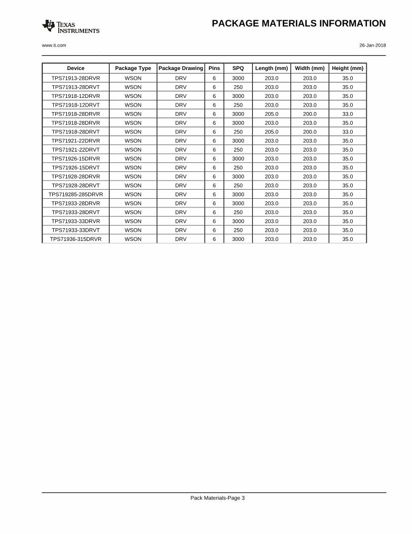
Device Package Type Package Drawing Pins SPQ Length (mm) Width (mm) Height (mm)
TPS71913-28DRVR WSON DRV 6 3000 203.0 203.0 35.0
TPS71913-28DRVT WSON DRV 6 250 203.0 203.0 35.0
TPS71918-12DRVR WSON DRV 6 3000 203.0 203.0 35.0
TPS71918-12DRVT WSON DRV 6 250 203.0 203.0 35.0
TPS71918-28DRVR WSON DRV 6 3000 205.0 200.0 33.0
TPS71918-28DRVR WSON DRV 6 3000 203.0 203.0 35.0
TPS71918-28DRVT WSON DRV 6 250 205.0 200.0 33.0
TPS71921-22DRVR WSON DRV 6 3000 203.0 203.0 35.0
TPS71921-22DRVT WSON DRV 6 250 203.0 203.0 35.0
TPS71926-15DRVR WSON DRV 6 3000 203.0 203.0 35.0
TPS71926-15DRVT WSON DRV 6 250 203.0 203.0 35.0
TPS71928-28DRVR WSON DRV 6 3000 203.0 203.0 35.0
TPS71928-28DRVT WSON DRV 6 250 203.0 203.0 35.0
TPS719285-285DRVR WSON DRV 6 3000 203.0 203.0 35.0
TPS71933-28DRVR WSON DRV 6 3000 203.0 203.0 35.0
TPS71933-28DRVT WSON DRV 6 250 203.0 203.0 35.0
TPS71933-33DRVR WSON DRV 6 3000 203.0 203.0 35.0
TPS71933-33DRVT WSON DRV 6 250 203.0 203.0 35.0
TPS71936-315DRVR WSON DRV 6 3000 203.0 203.0 35.0
PACKAGE MATERIALS INFORMATION
www.ti.com 26-Jan-2018
Pack Materials-Page 3
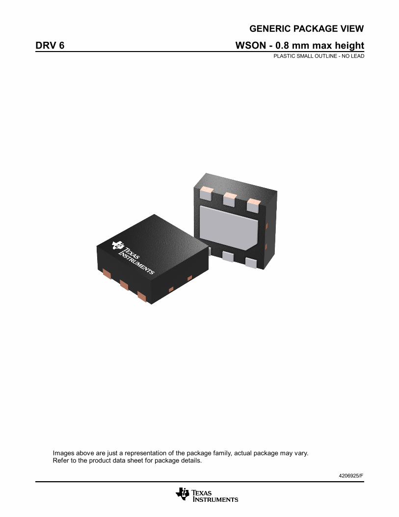
GENERIC PACKAGE VIEW
Images above are just a representation of the package family, actual package may vary.Refer to the product data sheet for package details.
DRV 6 WSON - 0.8 mm max heightPLASTIC SMALL OUTLINE - NO LEAD
4206925/F

www.ti.com
PACKAGE OUTLINE
C
6X 0.350.25
1.6 0.1
6X 0.30.2
2X1.3
1 0.1
4X 0.65
0.80.7
0.050.00
B 2.11.9
A
2.11.9
(0.2) TYP
WSON - 0.8 mm max heightDRV0006APLASTIC SMALL OUTLINE - NO LEAD
4222173/B 04/2018
PIN 1 INDEX AREA
SEATING PLANE
0.08 C
1
34
6
(OPTIONAL)PIN 1 ID
0.1 C A B0.05 C
THERMAL PADEXPOSED
7
NOTES: 1. All linear dimensions are in millimeters. Any dimensions in parenthesis are for reference only. Dimensioning and tolerancing per ASME Y14.5M. 2. This drawing is subject to change without notice. 3. The package thermal pad must be soldered to the printed circuit board for thermal and mechanical performance.
SCALE 5.500
www.ti.com
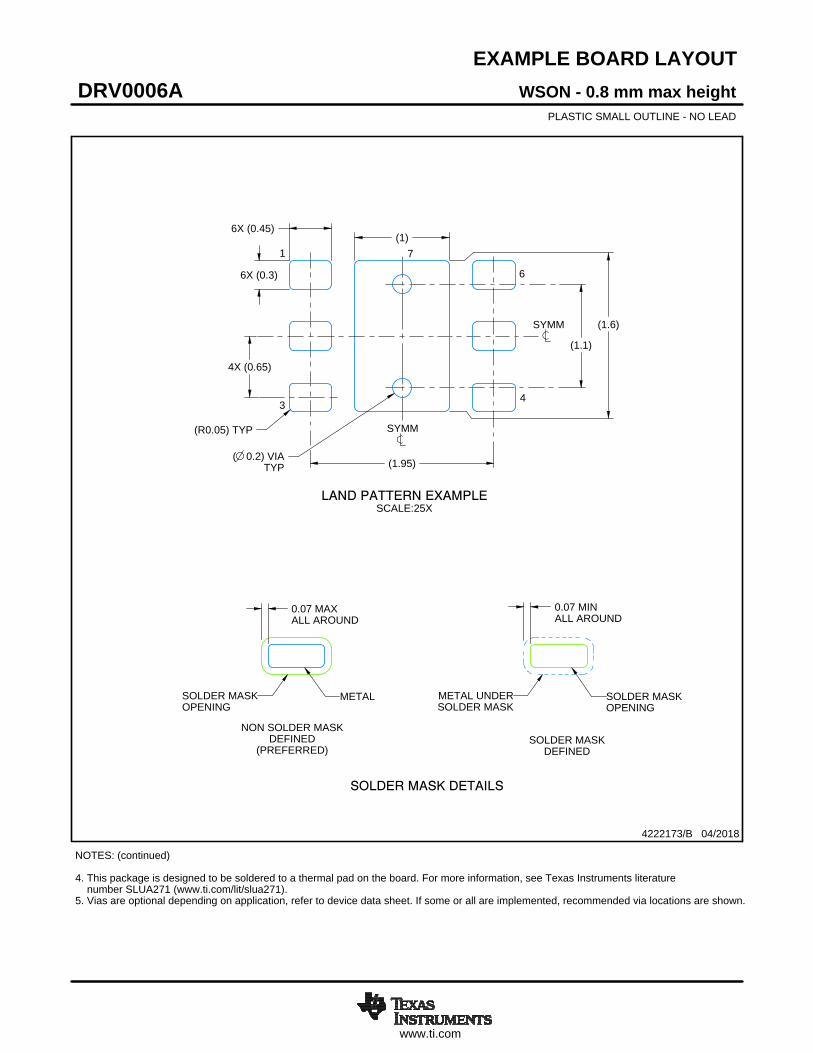
EXAMPLE BOARD LAYOUT
0.07 MINALL AROUND
0.07 MAXALL AROUND
(1)
4X (0.65)
(1.95)
6X (0.3)
6X (0.45)
(1.6)
(R0.05) TYP
( 0.2) VIATYP
(1.1)
WSON - 0.8 mm max heightDRV0006APLASTIC SMALL OUTLINE - NO LEAD
4222173/B 04/2018
SYMM
1
34
6
SYMM
LAND PATTERN EXAMPLESCALE:25X
7
NOTES: (continued) 4. This package is designed to be soldered to a thermal pad on the board. For more information, see Texas Instruments literature number SLUA271 (www.ti.com/lit/slua271).5. Vias are optional depending on application, refer to device data sheet. If some or all are implemented, recommended via locations are shown.
SOLDER MASKOPENINGSOLDER MASK
METAL UNDER
SOLDER MASKDEFINED
METALSOLDER MASKOPENING
SOLDER MASK DETAILS
NON SOLDER MASKDEFINED
(PREFERRED)
www.ti.com
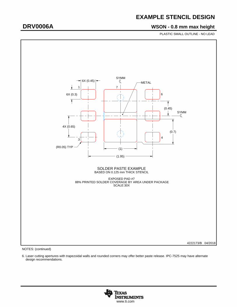
EXAMPLE STENCIL DESIGN
6X (0.3)
6X (0.45)
4X (0.65)
(0.7)
(1)
(1.95)
(R0.05) TYP
(0.45)
WSON - 0.8 mm max heightDRV0006APLASTIC SMALL OUTLINE - NO LEAD
4222173/B 04/2018
NOTES: (continued) 6. Laser cutting apertures with trapezoidal walls and rounded corners may offer better paste release. IPC-7525 may have alternate design recommendations.
SOLDER PASTE EXAMPLEBASED ON 0.125 mm THICK STENCIL
EXPOSED PAD #7
88% PRINTED SOLDER COVERAGE BY AREA UNDER PACKAGESCALE:30X
SYMM
1
3 4
6
SYMM
METAL7
IMPORTANT NOTICE
Texas Instruments Incorporated (TI) reserves the right to make corrections, enhancements, improvements and other changes to itssemiconductor products and services per JESD46, latest issue, and to discontinue any product or service per JESD48, latest issue. Buyersshould obtain the latest relevant information before placing orders and should verify that such information is current and complete.TI’s published terms of sale for semiconductor products (http://www.ti.com/sc/docs/stdterms.htm) apply to the sale of packaged integratedcircuit products that TI has qualified and released to market. Additional terms may apply to the use or sale of other types of TI products andservices.Reproduction of significant portions of TI information in TI data sheets is permissible only if reproduction is without alteration and isaccompanied by all associated warranties, conditions, limitations, and notices. TI is not responsible or liable for such reproduceddocumentation. Information of third parties may be subject to additional restrictions. Resale of TI products or services with statementsdifferent from or beyond the parameters stated by TI for that product or service voids all express and any implied warranties for theassociated TI product or service and is an unfair and deceptive business practice. TI is not responsible or liable for any such statements.Buyers and others who are developing systems that incorporate TI products (collectively, “Designers”) understand and agree that Designersremain responsible for using their independent analysis, evaluation and judgment in designing their applications and that Designers havefull and exclusive responsibility to assure the safety of Designers' applications and compliance of their applications (and of all TI productsused in or for Designers’ applications) with all applicable regulations, laws and other applicable requirements. Designer represents that, withrespect to their applications, Designer has all the necessary expertise to create and implement safeguards that (1) anticipate dangerousconsequences of failures, (2) monitor failures and their consequences, and (3) lessen the likelihood of failures that might cause harm andtake appropriate actions. Designer agrees that prior to using or distributing any applications that include TI products, Designer willthoroughly test such applications and the functionality of such TI products as used in such applications.TI’s provision of technical, application or other design advice, quality characterization, reliability data or other services or information,including, but not limited to, reference designs and materials relating to evaluation modules, (collectively, “TI Resources”) are intended toassist designers who are developing applications that incorporate TI products; by downloading, accessing or using TI Resources in anyway, Designer (individually or, if Designer is acting on behalf of a company, Designer’s company) agrees to use any particular TI Resourcesolely for this purpose and subject to the terms of this Notice.TI’s provision of TI Resources does not expand or otherwise alter TI’s applicable published warranties or warranty disclaimers for TIproducts, and no additional obligations or liabilities arise from TI providing such TI Resources. TI reserves the right to make corrections,enhancements, improvements and other changes to its TI Resources. TI has not conducted any testing other than that specificallydescribed in the published documentation for a particular TI Resource.Designer is authorized to use, copy and modify any individual TI Resource only in connection with the development of applications thatinclude the TI product(s) identified in such TI Resource. NO OTHER LICENSE, EXPRESS OR IMPLIED, BY ESTOPPEL OR OTHERWISETO ANY OTHER TI INTELLECTUAL PROPERTY RIGHT, AND NO LICENSE TO ANY TECHNOLOGY OR INTELLECTUAL PROPERTYRIGHT OF TI OR ANY THIRD PARTY IS GRANTED HEREIN, including but not limited to any patent right, copyright, mask work right, orother intellectual property right relating to any combination, machine, or process in which TI products or services are used. Informationregarding or referencing third-party products or services does not constitute a license to use such products or services, or a warranty orendorsement thereof. Use of TI Resources may require a license from a third party under the patents or other intellectual property of thethird party, or a license from TI under the patents or other intellectual property of TI.TI RESOURCES ARE PROVIDED “AS IS” AND WITH ALL FAULTS. TI DISCLAIMS ALL OTHER WARRANTIES ORREPRESENTATIONS, EXPRESS OR IMPLIED, REGARDING RESOURCES OR USE THEREOF, INCLUDING BUT NOT LIMITED TOACCURACY OR COMPLETENESS, TITLE, ANY EPIDEMIC FAILURE WARRANTY AND ANY IMPLIED WARRANTIES OFMERCHANTABILITY, FITNESS FOR A PARTICULAR PURPOSE, AND NON-INFRINGEMENT OF ANY THIRD PARTY INTELLECTUALPROPERTY RIGHTS. TI SHALL NOT BE LIABLE FOR AND SHALL NOT DEFEND OR INDEMNIFY DESIGNER AGAINST ANY CLAIM,INCLUDING BUT NOT LIMITED TO ANY INFRINGEMENT CLAIM THAT RELATES TO OR IS BASED ON ANY COMBINATION OFPRODUCTS EVEN IF DESCRIBED IN TI RESOURCES OR OTHERWISE. IN NO EVENT SHALL TI BE LIABLE FOR ANY ACTUAL,DIRECT, SPECIAL, COLLATERAL, INDIRECT, PUNITIVE, INCIDENTAL, CONSEQUENTIAL OR EXEMPLARY DAMAGES INCONNECTION WITH OR ARISING OUT OF TI RESOURCES OR USE THEREOF, AND REGARDLESS OF WHETHER TI HAS BEENADVISED OF THE POSSIBILITY OF SUCH DAMAGES.Unless TI has explicitly designated an individual product as meeting the requirements of a particular industry standard (e.g., ISO/TS 16949and ISO 26262), TI is not responsible for any failure to meet such industry standard requirements.Where TI specifically promotes products as facilitating functional safety or as compliant with industry functional safety standards, suchproducts are intended to help enable customers to design and create their own applications that meet applicable functional safety standardsand requirements. Using products in an application does not by itself establish any safety features in the application. Designers mustensure compliance with safety-related requirements and standards applicable to their applications. Designer may not use any TI products inlife-critical medical equipment unless authorized officers of the parties have executed a special contract specifically governing such use.Life-critical medical equipment is medical equipment where failure of such equipment would cause serious bodily injury or death (e.g., lifesupport, pacemakers, defibrillators, heart pumps, neurostimulators, and implantables). Such equipment includes, without limitation, allmedical devices identified by the U.S. Food and Drug Administration as Class III devices and equivalent classifications outside the U.S.TI may expressly designate certain products as completing a particular qualification (e.g., Q100, Military Grade, or Enhanced Product).Designers agree that it has the necessary expertise to select the product with the appropriate qualification designation for their applicationsand that proper product selection is at Designers’ own risk. Designers are solely responsible for compliance with all legal and regulatoryrequirements in connection with such selection.Designer will fully indemnify TI and its representatives against any damages, costs, losses, and/or liabilities arising out of Designer’s non-compliance with the terms and provisions of this Notice.
Mailing Address: Texas Instruments, Post Office Box 655303, Dallas, Texas 75265Copyright © 2018, Texas Instruments Incorporated