Embed Size (px)
Citation preview

Dual Input DC-DC Converter for Renewable Energy SystemsA. Lavanya*, Nivas Jayaseelan**, J. Divya Navamani*** and Vijayakumar.K****
Abstract: This paper proposes a dual input high step-up boost converter for grid-connected photovoltaic power generation system. Four different DC-DC converters are considered for analysis. From the result of the analysis, the converter with reduced component count and current ripple is identified and proposed for the grid connected PV power generation system. Next, the mode of operation of the proposed converter is discussed along with its circuit modeling and performances are analyzed in detail. The proposed converter is analyzed using MATLAB simulations. The proposed converter includes multiplier cells which boosts the converter to a high step voltage. Finally, closed loop control is performed with a PI controller. This is done in order to keep the output voltage constant.
Index Terms: High voltage gain dc-dc power electronic converters, closed loop control, PI Controller.
1. INTRODUCTIONFinding renewable and clean energy sources is important for the gradual depletion of primary energy and environmental problems. Since renewable energy is cleaner and more reliable, renewable energy generation has attracted more and more attention and research. Recently, the grid-connected PV power generation system has been developed promptly, especially in Europe [1]. Also, the newly opened solar power plant in Tamilnadu is the largest solar power plant in the world in terms of area and power generation capacity. It has been expected to be one of the most important power-generated modes in the foreseeable future.
Multiple-Input energy sources have the capability of diversifying different energy sources and increasing the reliability of the system. MI converters can combine the advantages of different sources, such as photovoltaic cells, fuel cells, batteries, ultra-capacitors, and other renewable energy sources, with different voltage and current characteristics for optimal energy/economic use. A lot of research has gone to analysis, modelling, and utilizing MI converters in applications such as grid-connected integrated hybrid generation systems, fuel cells, micro-grid based telecom power systems, uninterruptible power supplies, and electric and hybrid electric vehicles[2].
The main focus of this paper is to design a multiple-input hybrid energy conversion topology with closed loop control in order to get a constant output voltage.
This paper is organised as follows. The topology of the high step-up boost converter with dual input is presented in Section II. The mathematical modelling of the proposed converter is presented in Section III. Design of the proposed converter is presented in Section IV. Section V calculates the current ripple of the converter topology. Section VI explains the closed loop operation and need. Experimental results with 230 V output is given in Section VII. Section VIII summarises the conclusions drawn from the proposed converter topology.
* Assistant Professor, EEE, SRM University, Kattankulathur, India** P.G. Scholar, EEE, SRM University, Kattankulathur, India*** Assistant Professor, EEE, SRM University, Kattankulathur, India**** Professor, EEE, SRM University, Kattankulathur, India
I J C T A, 9(37) 2016, pp. 911-921© International Science Press

912 A. Lavanya, Nivas Jayaseelan, J. Divya Navamani and Vijayakumar.K
2. TOPOLOGYThe topology of conventional boost converter is shown in Figure 1. The gain of the conventional boost converter can be represented as
MD
=-1
1 (1)
Where D is the duty cycle
Figure 1: Conventional Boost Converter
Capacitors can be used as a voltage source since the ripple of the voltage across the capacitor can be neglected when compared with its DC value. A voltage source cannot be substituted directly with a capacitor. Doing this may not be advisable since the converter cannot operate in steady state, due to its inability to satisfy the ampere–second balance requirement of the capacitor. Eventually, the converter will be damaged.
The proposed converter is a high step up boost converter with dual input and contains two switches and is shown in Figure 2.
Figure 2: High Step Up Boost Converter with Dual Input
When S1 is ON and S2 is OFF, C1 is charged, when switch S1 is OFF and S2 is ON, capacitor C1 is discharged. Here, it is possible to satisfy the ampere–second balance requirement of C1 in one switch period Ts
Figure 1 shows a high step up boost converter with one voltage multiplier. Depending upon the gain, it can step up the voltage. Gain for the proposed converter can be calculated by the formula shown in (1). It can be noted that the gain is double than that of the conventional boost converter.
MD
=-2
1 (2)
The pulses used in the proposed circuit a pulse width of 70%.
The pulse width is chosen as such since the utilization factor of the switches is the highest at 70%. For the dual input boost converter, the utilization factor can be calculated by,

913Dual Input DC-DC Converter for Renewable Energy Systems
Figure 3: Pulses given to the switches
UPSload= (3)
S is the switch stress and it can be calculated by,
S I==Â v j jj
k
1 (4)
The utilization factor is calculated for various duty ratios and is represented in the Figure 4.
When the input voltage is set at 35V, the output voltage obtained is 230V. This value is almost equal to the theoretical value calculated from (2). The output voltage waveform is shown in Figure 9.
Figure 4: Utilization Factor
3. MATHEMATICAL MODELING OF THE PROPOSED CONVERTERModeling has been done using the current and voltage equations in order to compare the results of the block simulation with modeling simulation results. (5) and (6) show the voltage equations
V1D1 = (V0 - Vc1 - V1)(1 - D1) (5)
V2D2 = (Vc1 - V2)(1 - D2) (6)
The capacitance voltage is given in the (7). (8) calculates the output voltage of the circuit.
Vc1 = VD1
21( )- (7)
V0 = VD
VD
1
1
2
21 1( ) ( )-+
- (8)

914 A. Lavanya, Nivas Jayaseelan, J. Divya Navamani and Vijayakumar.K
Since both the duty cycle is kept constant at 70%, both of them are equal. Hence,
D1 = D2 = D (9)
Similarly, the voltages are also kept constant. Hence,
V1 = V2 = V (10)
From the above equations, the following equations are obtained. They are labeled from (11) to (14)
ddtIL1 = VD V D V D V D1 + - - - - -0 1 11 1 1( ) ( ) ( )c (11)
ddtIL2 = ( ) ( )V V D V Dc1 2 2 1- + - (12)
ddtV0 =
-- + -Ê
ËÁˆ¯̃
-VR
D IVRL100 1 1( ) ( )D (13)
ddtVC1 = I D I DL2 L1( ) ( )1 1- + - (14)
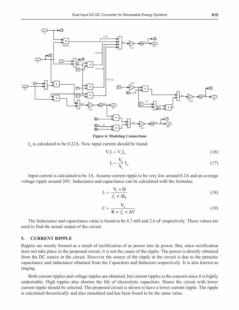
The above equations from (11) to (14) are used to construct model blocks. The modeling connections are shown is Figure 5 and 6.
Figure 5: Voltage Input and Pulse Generation
The two inputs and the Pulse is given to the main circuit which has been kept inside the subsystem. The Pulse generation is done using PWM generation. The repeating sequence is the key factor to creating the pulse. The content inside the subsystem is shown in the Figure 6.
The Output Voltage of the modeled circuit is obtained through a scope and recorded. The output voltage is similar to the simulated waveform and is 230V.
4. DESIGN OF THE PROPOSED CONVERTERAssume the value of the output power to be 50W and the output voltage to be 230V since the application of this converter requires connecting to the grid.
Io = PV
o
o (15)
915Dual Input DC-DC Converter for Renewable Energy Systems
Figure 6: Modeling Connections
Io is calculated to be 0.22A. Now input current should be found.
ViIi = VoIo (16)
Ii = VVIo
io (17)
Input current is calculated to be 3A. Assume current ripple to be very low around 0.2A and an average voltage ripple around 20V. Inductance and capacitance can be calculated with the formulae.
L = V D
ILi
sf¥
¥ D (18)
C = V
R Vo
sf¥ ¥ D (19)
The Inductance and capacitance value is found to be 4.7 mH and 2.6 uF respectively. These values are used to find the actual output of the circuit.
5. CURRENT RIPPLERipples are mostly formed as a result of rectification of ac power into dc power. But, since rectification does not take place in the proposed circuit, it is not the cause of the ripple. The power is directly obtained from the DC source in the circuit. However the source of the ripple in the circuit is due to the parasitic capacitance and inductance obtained from the Capacitors and Inductors respectively. It is also known as ringing.
Both current ripples and voltage ripples are obtained, but current ripples is the concern since it is highly undesirable. High ripples also shorten the life of electrolytic capacitors. Hence the circuit with lower current ripple should be selected. The proposed circuit is shown to have a lower current ripple. The ripple is calculated theoretically and also simulated and has been found to be the same value.

916 A. Lavanya, Nivas Jayaseelan, J. Divya Navamani and Vijayakumar.K
The ripple in the current can be calculated by the
DIL = V DF Lin ¥
¥s (20)
The Supply Voltage is 35V. Since, a duty ratio of 0.7 was considered to be optimum from Figure 4, the value has been selected. Supply frequency should be high, so 30 KHZ is selected. During the design, inductance of 500uH had been selected. Substituting these values in the equation, we get,
DIL = 35 0 730000 500 6
¥¥ -
.e (21)
DIL = 1.63 A (22)
When the circuit is simulated, the current ripple is taken and shown in Figure 7. The current ripple in the simulated waveform appears to the same value as in the theoretical calculation. This value is lesser then the other converters that has been studied during the project.
Figure 7: Current Ripple
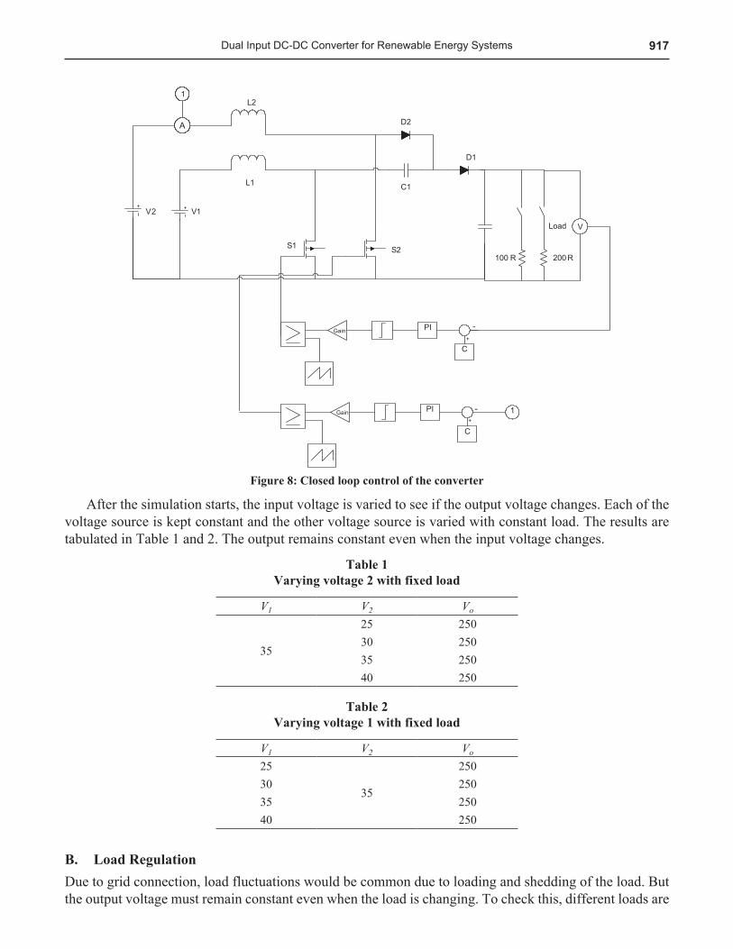
6. CLOSED LOOP TOPOLOGY OF THE PROPOSED CONVERTERThe input to this converter would be renewable energy like Photovoltaic cells or wind turbines. Hence, the input voltage to the converter would be inconsistent and would have lots of wavering. This will cause the output voltage to change. The output is connected to grid applications and hence requires a constant output. To get a constant output voltage Vo, a feedback system is necessary.
PI controllers can be used as a feedback system to keep the output voltage constant by using a reference voltage.
The closed loop control is done using a PI controller. The output voltage is taken and compared to a reference value and creates an error. This error is used as an input to the PI controller. PWM is used to create the pulses and given to the switch as a gate pulse. Whenever the voltage changes, the output voltage will also change, but the error in voltage change will alter the pulse given to the switch, hence keeping the output voltage constant. The construction of the closed loop control is shown in Figure 8.There are two methods performed to see if the closed loop control works:• By keeping the load constant and varying the voltage.• By keeping the voltage constant and varying the load.
A. Line RegulationSince the voltage sources are renewable energy sources like solar and wind, there is large chance that the input voltage will keep varying. For grid connecting applications, maintaining a constant voltage is mandatory. To ensure that the output voltage remains constant, PI control is performed.
917Dual Input DC-DC Converter for Renewable Energy Systems
Figure 8: Closed loop control of the converter
After the simulation starts, the input voltage is varied to see if the output voltage changes. Each of the voltage source is kept constant and the other voltage source is varied with constant load. The results are tabulated in Table 1 and 2. The output remains constant even when the input voltage changes.
Table 1 Varying voltage 2 with fixed load
V1 V2 Vo
35
25 250 30 250 35 250 40 250
Table 2 Varying voltage 1 with fixed load
V1 V2 Vo
25
35
250 30 250 35 250 40 250
B. Load RegulationDue to grid connection, load fluctuations would be common due to loading and shedding of the load. But the output voltage must remain constant even when the load is changing. To check this, different loads are

918 A. Lavanya, Nivas Jayaseelan, J. Divya Navamani and Vijayakumar.K
connected to the simulation with switches. Since load cannot be changed when the simulation is running, two different loads are connected with a switch in series with each load. The switches are switched automatically to check the output voltage.
Table 3 Varying load with fixed input voltages
Load (Ohms) Vo
100 25066.67 250200 250
66.67 250100 250
7. EXPERIMENTAL VERIFICATIONSThe output voltage of the open loop system obtained is 230 V. The voltage waveform is shown in Figure 9.
Figure 9: Output Voltage
The current in inductors are affected by the pulses. Whenever the amplitude of the pulse increases, the current also increases and when the pulse decreases, the current decreases. The current of inductor1 is affected by P1 and current of inductor 2 is affected by P2. The Inductor current is shown in Figure 10.
It can be noted that the inductor currents are same for both the inductors in terms of amplitude and pattern. But the diode current and switch currents are different. (i.e) ID1 and ID2 are different. Similarly IS1 and IS2 are different. This is due to the fact that the both are unsymmetrical since both carry different current values. ID2 is wider than ID1 because it carries more load. Similarly, IS1 carries more loads since the diode current passes though this S1 and no diode current pass through S2. Both diode currents and switch currents are shown in Figure 11.
After connecting PI controller, the output remains constant and takes the value of the reference in PI controller. Once the reference value and the output value get loop locked, the output value remains constant even when the input voltage is changed. Two examples have been shown. When the reference value is fixed at 200V, the output stays at 200V after the loop lock and this is shown in Figure 12. Similarly, the output waveform for 300V reference value is shown in Figure 13.

919Dual Input DC-DC Converter for Renewable Energy Systems
Figure 10: Inductor Current
Figure 11: Diode and Switch Currents
8. CONCLUSIONThe closed loop controller topologies for the proposed dual input boost converter has been described in this work. Four converters has been compared and analyzed. From the result of the analysis, the converter with reduced component count and current ripple has identified for the grid connected PV power generation system. The proposed converter has 1.24% lesser ripple and slightly higher gain of 0.3% than the parallel connected boost converter. The mode of operation of the proposed converter has been discussed along with its circuit modeling and performances are analyzed in detail. A PI controller has been implemented in order to maintain the output voltage constant to the reference value. The output response of the proposed open loop and closed loop has been studied. It is inferred that the output is maintained constant with respect

920 A. Lavanya, Nivas Jayaseelan, J. Divya Navamani and Vijayakumar.K
to input variation in the closed loop topology due to the propotional integral action of PI controller. The operation and performance of the converter has been done using MATLAB simulations.
Figure 12: Output Voltage (Reference 200V)
Figure 13: Output Voltage (Reference 300V)
References1. L.W. Zhou, B.X Zhu and Q.M. Luo, “High step-up converter with capacity of multiple input,” IET Power Electronics,
Vol. 5, No. 5, pp. 524-531, 2012.2. Alireza Khaligh, Jian Cao and Young-Joo Lee, “A Multiple-Input DC-DC Converter Topology,” IEEE Transactions On
Power Electronics, Vol. 24, No. 3, pp. 862-868, Mar 2009.3. Venkata Anand Kishore Prabhala, Poria Fajri, Venkat Sai Prasad Gouribhatla, Bhanu Prashant Baddipadiga and Mehdi
Ferdowsi, “A DC-DC Converter With High Voltage Gain and Two Input Boost Stages,” IEEE Transactions On Power Electronics, Vol. 31, No. 6, June 2016.
4. Zubair Rehman, IbrahimAl-Bahadly and Subhas Mukhopadhyay, “Multi - input DC-DC converters in renewable energy applications – An overview,” Renewable and Sustainable Energy Reviews, Vol. 41, pp. 521-539, Aug 2014.
5. Hongfei Wu, Peng Xu, Haibing Hu, Zihu Zhou and Yan Xing, “Multiport Converters Based on Integration of Full-Bridge and Bidirectional DC-DC Topologies for Renewable Generation Systems,” IEEE Transactions On Industrial Electronics, Vol. 61, No. 2, Feb 2014.

921Dual Input DC-DC Converter for Renewable Energy Systems
6. Yen Mo Chen, Alex Q Huang and Xunwei Yu, “A High Step-Up Three-Port DC-DC Converter for Stand-Alone PV/Battery Power Systems,” IEEE Transactions On Power Electronics, Vol. 28, No. 11, Nov 2013.
7. Rong-Jong Wai, Chung-You Lin and Bo-Han Chen, “High-Efficiency DC-DC Converter with Two Input Power Sources,” IEEE Transactions On Power Electronics, Vol. 27, No. 4, Apr 2012.
8. Yaow-Ming Chen, Yuan-Chuan Liu and Sheng-Hsien Lin, “Double-Input PWM DC/DC Converter for High/Low Voltage Sources,” IEEE Transactions On Power Electronics, Vol. 27, No. 4, Apr 2012.
9. S. Lee, P. Kim, and S. Choi, “High step-up soft-switched converters using voltage multiplier cells,” IEEE Transactions On Power Electronics, Vol. 28, No. 7, pp. 3379-3387, Jul. 2013.
10. K.C. Tseng and C.C. Huang, “High step-up high-efficiency interleaved converter with voltage multiplier module for renewable energy system,” IEEE Transactions On Industrial Electronics, Vol. 61, No. 3, pp. 1311-1319, Mar. 2014.
11. S. Lee, P. Kim and S. Choi, “High step-up soft-switched converters using voltage multiplier cells,” IEEE Transactions On Power Electronics, Vol. 28, No. 7, pp. 3379-3387, Jul. 2013.
12. B. G. Dobbs and P. L. Chapman, “A multiple-input DC-DC converter,” IEEE Power Electronics Letter, Vol. 1, No. 1, pp. 6-9, Mar. 2003.
13. H. Matsuo, L. Wenzhong, F. Kurokawa, T. Shigemizu and N. Watanabe, “Characteristics of the multiple-input dc-dc converter,” IEEE Transaction on Industrial Electronics, Vol. 51, No. 3, pp. 625-631, Jun. 2004.
14. Hongfei Wu, Junjun Zhang and Yan Xing, “A Family of Multiport Buck-Boost Converters Based on DC-Link-Inductors”, IEEE Transactions On Power Electronics, Vol. 30, No. 2, Feb 2015.
15. Liand W and He W, “Review of Non-Isolated High Step-Up DC/DC Converters in Photovoltaic Grid-Connected Applications,” IEEE Transaction on Industrial Electronics, vol 58, No. 4, pp. 1239-1250, Apr 2011.
16. Wai R.J, Wang W.H. and Lin C.Y, “High-Performance Stand-Alone Photo Voltaic Generation System,” IEEE Transaction on Industrial Electronics, Vol. 55, No. 1, pp. 240-250, Jan 2008.
17. B. G. Dobbs and P. L. Chapman, “A multiple-input DC-DC converter,” IEEE Power Electronics Letter, Vol. 1, No. 1, pp. 6-9, Mar. 2003.
18. H. Matsuo, L. Wenzhong, F. Kurokawa, T. Shigemizu, and N. Watanabe, “Characteristics of the multiple-input dc-dc converter,” IEEE Transaction on Industrial Electronics, Vol. 51, No. 3, pp. 625-631, Jun. 2004.
19. Qun Z and Lee, F.C, “High-efficiency, high step-up DC-DC converters” IEEE Transactions on Power Electronics, Vol. 18, No. 1, pp. 35-73, May 2003.
20. Li W and He X, “ZVT interleaved boost converters for high efficiency, high step-up DC-DC conversion,” IET Power Electronics, Vol. 1, no 2, pp. 284-290, Jul 2007.
21. Walker G.R, Sernia P.C, “Cascaded DC-DC converter connection of photovoltaic modules,” IEEE Transactions on Power Electronics, Vol. 19, No. 4, pp. 1130-1139, Mar 2004.
22. Tseng S.Y and Ou C.L, “Interleaved coupled-inductor boost converter with boost type snubber for PV system,” Energy Conversion Congress and Exposition, pp. 1860-1867, 2009.
23. Dwari S and Parsa, L, “A novel high efficiency high power interleaved coupled-inductor Boost DC-DC converter for hybrid and fuel cell electric vehicle,” IEEE Vehicle Power and Propulsion Conference, pp. 399-404, sep 2007.
24. Wai R.J and Duan R.Y, “High step-up converter with coupled-inductor,” IEEE Transactions on Power Electronics, Vol. 20, No. 5, pp. 1025-1035, Apr 2005.
25. Shenkman A, Berkovich Y and Axelrod B, “Novel AC–DC and DC-DC converters with a diode-capacitor multiplier,” IEEE Transactions on Aerospace and Electronic Systems, Vol. 40, No. 4, pp. 1286-1293, Jan 2005.
26. Prudente M, Pfitscher L.L, Emmendoerfer G, Romaneli E.F.R, and Gules R “Voltage multiplier cells applied to non-isolated DC-DC converters,” IEEE Transactions on Power Electronics, Vol. 23, No. 2, pp. 871-887, Mar 2008.
27. Sanghyuk L, Pyosoo K and Sewan C, “High step-up soft-switched converters using voltage multiplier cells.” IEEE Transactions on Power Electronics, Vol. 28, No. 7, pp. 3379-3387, Jul 2013.
28. L.W Zhou, B.X Zhu and Q.M Luo, “High step-up converter with capacity of multiple input,” IET Power Electronics, Vol. 5, No. 5, pp. 524-531, May 2012.
29. Kwasinski A, “Identification of Feasible Topologies for Multiple-Input DC-DC Converters,” IEEE Transactions on Power Electronics, Vol. 24, No. 3, pp. 856-861, Mar 2009.
30. Rong-Jong Wai, Chung-You Lin and Bo-Han Chen, “High-Efficiency DC-DC Converter With Two Input Power Sources,” IEEE Transactions On Power Electronics, Vol. 27, No. 4, pp.1862-1875, Apr 2012.