Embed Size (px)
Citation preview

l Q QT1100A-ISGADVANCED INFORMATION 10 KEY QTOUCH™ SENSOR IC
APPLICATIONSAppliance controlsPointing devicesGaming machines
PC peripheralsTelevision controlsInstrument panels
QT1100A charge-transfer (“QT”) QTouch ICs are self-contained digital controllers capable of detecting near-proximity or touch on up to10 electrodes. This device allows each electrode to project an independent sense field through glass or plastic. These devices requireonly a few inexpensive passive components per sensing channel. The devices are designed specifically for human interfaces, such ascontrol panels, appliances, gaming devices, lighting controls, or anywhere a mechanical switch may be found.
Each key channel operates independently, and can be tuned to a unique sensitivity level by simply changing setup values in anEEPROM or via a serial interface. An external EEPROM can store the setups permanently for standalone applications, for examplewhen using the scanport, or, the EEPROM can be omitted if the serial port is used to send setup information after each power-up.
Included is patent pending AKS™ Adjacent Key Suppression which suppresses touch from weakly responding keys and allows only adominant key to detect, to solve the problem of large fingers on tightly spaced keys. Modulated burst technology provides superiornoise rejection. ‘Fast-DI’ operation works to further suppress false activations due to noise.
These devices also have a Sync pin to suppress some forms of external interference. A Sleep mode is also available for very lowpower standby operation.
The QT1100A is designed specifically to assist in creating FMEA compliant designs, allowing it to be used in applications such asappliance controls.
Using the charge transfer principle, these devices deliver a level of performance which is clearly superior to older technologies yetextremely cost-effective.
L Q 1 Copyright © 2003-2005 QRG LtdQT1100A-ISG R3.01/0505
10 independent touch sensing fields100% autocal for life - no adjustments requiredSPI and UART serial interfacesScanport output - simulates a membrane keypadSimple external per channel passive circuit User-defined setups of operating parameters3.3V~5.0V single supply operationAKS™ Adjacent Key Suppression for tight key layoutsSleep mode for low power operationSpread spectrum modulated bursts - superior noise rejectionSync pin for superior mains frequency noise rejectionFMEA compliant design features - self detects faultsLower per key cost than many mechanical switchesLead-free package
YesQT1100A-ISG-40ºC to +85ºCLEAD-FREESSOP-48TA
AVAILABLE OPTIONS
Actual Size
193.5.2 Reference for Key ‘k’ - 0x4k . . . . . . . . . . . . . . . . . .193.5.1 Signal for 1 Key - 0x2k . . . . . . . . . . . . . . . . . . . . .193.5 Status Commands . . . . . . . . . . . . . . . . . . . . . . .193.4.7 Cal Key ‘k’ - 0x1k . . . . . . . . . . . . . . . . . . . . . . .183.4.6 Sleep - 0x05 . . . . . . . . . . . . . . . . . . . . . . . . .183.4.5 Force Reset - 0x04 . . . . . . . . . . . . . . . . . . . . . .183.4.4 Enter Cal Mode - 0x03 . . . . . . . . . . . . . . . . . . . . .183.4.3 Enter Run Mode - 0x02 . . . . . . . . . . . . . . . . . . . .173.4.2 Enter Setups Load Mode - 0x01 . . . . . . . . . . . . . . . . .173.4.1 Null Command - 0x00 . . . . . . . . . . . . . . . . . . . . .173.4 Control Commands . . . . . . . . . . . . . . . . . . . . . . .163.3 Communication Error Handling . . . . . . . . . . . . . . . . .163.2.3 CRDY Operation in SPI Mode . . . . . . . . . . . . . . . . . .163.2.2 Sleep/Wake Operation in SPI Mode . . . . . . . . . . . . . . .163.2.1 Multi-Drop SPI Capability . . . . . . . . . . . . . . . . . . . .163.2 SPI Operation . . . . . . . . . . . . . . . . . . . . . . . . . .153.1.3 CRDY Operation in UART Mode . . . . . . . . . . . . . . . .153.1.2 Sleep/Wake Operation in UART Mode . . . . . . . . . . . . . .153.1.1 TX Pin . . . . . . . . . . . . . . . . . . . . . . . . . . . .153.1 UART Interface . . . . . . . . . . . . . . . . . . . . . . . . .153 Serial Operation . . . . . . . . . . . . . . . . . . . . . . . . .142.16 Error Detection and Reporting . . . . . . . . . . . . . . . . .142.15 Start-up Sequencing . . . . . . . . . . . . . . . . . . . . . .142.14 Scanport Interface . . . . . . . . . . . . . . . . . . . . . . .142.13 EEPROM Functionality . . . . . . . . . . . . . . . . . . . . .142.12 Standalone Operation, No EEPROM . . . . . . . . . . . . . .132.11 Operating Parameter Setups . . . . . . . . . . . . . . . . . .132.10 Start-up Time . . . . . . . . . . . . . . . . . . . . . . . . .132.9.2 External Fields . . . . . . . . . . . . . . . . . . . . . . . .132.9.1 LED Traces and Other Switching Signals . . . . . . . . . . . . .132.9 Noise Issues . . . . . . . . . . . . . . . . . . . . . . . . . .132.8 ESD Protection . . . . . . . . . . . . . . . . . . . . . . . . .122.7 PCB Layout and Construction . . . . . . . . . . . . . . . . . .122.6 Power Supply . . . . . . . . . . . . . . . . . . . . . . . . . .122.5 Sensitivity Balance . . . . . . . . . . . . . . . . . . . . . . .122.4 Sensitivity . . . . . . . . . . . . . . . . . . . . . . . . . . . .122.3 Cs Sample Capacitors . . . . . . . . . . . . . . . . . . . . . .122.2 Spread Spectrum Modulation . . . . . . . . . . . . . . . . . .122.1 Oscillator . . . . . . . . . . . . . . . . . . . . . . . . . . . .122 Device Control & Wiring . . . . . . . . . . . . . . . . . . . .11Figure 1.3 Scanport Only Connection Diagram+ . . . . . . . . . . .10Figure 1.2 UART / Scanport Connection Diagram . . . . . . . . . .9Figure 1.1 SPI Connection Diagram . . . . . . . . . . . . . . . . .8Table 1.5 Pin Descriptions . . . . . . . . . . . . . . . . . . . . . .7Table 1.4 SPI Pinlist . . . . . . . . . . . . . . . . . . . . . . . . .6Table 1.3 Standalone Pinlist . . . . . . . . . . . . . . . . . . . . .5Table 1.2 Standalone Pinlist . . . . . . . . . . . . . . . . . . . . .4Table 1.1 Scanport / UART Pinlist . . . . . . . . . . . . . . . . . .31 Overview . . . . . . . . . . . . . . . . . . . . . . . . . . . . . .
416 Appendix A - 8-Bit CRC C Algorithm . . . . . . . . . . . . .405.10 Marking . . . . . . . . . . . . . . . . . . . . . . . . . . . .405.9 Mechanical . . . . . . . . . . . . . . . . . . . . . . . . . . .405.8 Current vs Vdd . . . . . . . . . . . . . . . . . . . . . . . . .395.7 QT1100A Timing Parameters - with Fosc = 12MHz . . . . . . .385.6 SPI Timing Diagram . . . . . . . . . . . . . . . . . . . . . .375.5 Burst / Sync Timing . . . . . . . . . . . . . . . . . . . . . . .365.4 DC Specifications . . . . . . . . . . . . . . . . . . . . . . . .365.3 AC Specifications . . . . . . . . . . . . . . . . . . . . . . . .365.2 Recommended Operating Conditions . . . . . . . . . . . . . .365.1 Absolute Maximum Specifications . . . . . . . . . . . . . . . .365 - Specifications . . . . . . . . . . . . . . . . . . . . . . . . . .324.17 Timing Tables . . . . . . . . . . . . . . . . . . . . . . . . .31Table 4-1 Serial / EEPROM Setups Block . . . . . . . . . . . . . .304.16 HCRC - Host CRC . . . . . . . . . . . . . . . . . . . . . . .294.15 BR - Baud Rate Control Bits . . . . . . . . . . . . . . . . . .294.14 BS - Burst Spacing Control Bits . . . . . . . . . . . . . . . .294.13 LBLL - Lower Burst Length Limit . . . . . . . . . . . . . . . .284.12 SE, SYNC Control Bits . . . . . . . . . . . . . . . . . . . . .284.11 PHYS - Positive Hysteresis Bits . . . . . . . . . . . . . . . .284.10 PTHR - Positive Threshold Bits . . . . . . . . . . . . . . . . .274.9 NDIL, FDIL - Detect Integrator Bits . . . . . . . . . . . . . . . .274.8 K2L / LEDP / KEYO Control Bits . . . . . . . . . . . . . . . . .274.7 EK - Error Key Control Bits . . . . . . . . . . . . . . . . . . .264.6 AKS - Adjacent Key Suppression Bits . . . . . . . . . . . . . .264.5 PRD - Positive Recal Delay Bits . . . . . . . . . . . . . . . . .264.4 NRD - Negative Recal Delay Bits . . . . . . . . . . . . . . . .254.3 NDCR / PDCR - Drift Comp Bits . . . . . . . . . . . . . . . . .254.2 NHYS - Negative Hysteresis Bits . . . . . . . . . . . . . . . .254.1 NTHR - Negative Threshold Bits . . . . . . . . . . . . . . . . .254 Setup Block Functions . . . . . . . . . . . . . . . . . . . . .24Table 3-2 Status Commands . . . . . . . . . . . . . . . . . . . .23Table 3-1 Control Commands . . . . . . . . . . . . . . . . . . . .22Figure 3-1 Suggested Serial Flow . . . . . . . . . . . . . . . . . .213.6 Command Sequencing . . . . . . . . . . . . . . . . . . . . .213.5.14 Quick Report First Key - 0xC9 . . . . . . . . . . . . . . . . .213.5.13 Dump Setups Block - 0xC8 . . . . . . . . . . . . . . . . . .213.5.12 Return Last Command - 0xC7 . . . . . . . . . . . . . . . . .213.5.11 Internal Code - 0xC6 . . . . . . . . . . . . . . . . . . . . .213.5.10 Error Flags for Group - 0xC5 . . . . . . . . . . . . . . . . .203.5.9 RAM CRC - 0xC4 . . . . . . . . . . . . . . . . . . . . . . .203.5.8 EEPROM CRC - 0xC3 . . . . . . . . . . . . . . . . . . . . .203.5.7 Device Status - 0xC2 . . . . . . . . . . . . . . . . . . . . .203.5.6 Report All Keys - 0xC1 . . . . . . . . . . . . . . . . . . . . .203.5.5 Report 1st Key - 0xC0 . . . . . . . . . . . . . . . . . . . . .193.5.4 Status for Key ‘k’ - 0x8k . . . . . . . . . . . . . . . . . . . .193.5.3 Detect Integrator for Key ‘k’ - 0x6k . . . . . . . . . . . . . . . .
L Q 2 Copyright © 2003-2005 QRG LtdQT1100A-ISG R3.01/0505
Contents
1 OverviewThe QT1100A is a 10 touch-key sensor IC based onQuantum’s patented charge-transfer principles for robustoperation and ease of design. This device has manyadvanced features which provide for reliable, trouble-freeoperation over the life of the product. It can operate in eithera standalone mode or under host control via a serialinterface. Output options include UART and SPI serial typesand parallel scanport. In any interface mode, a low-costoptional EEPROM can be used to determine the deviceconfiguration using a stored Setup block.
FMEA self-testing: This part has been designed specificallyfor demanding appliance applications requiring FMEAcertification. The part has many advanced features thatcheck for and report failures, to allow the designer to createa safer product. It also features two robust serial interfaceswith sophisticated CRC error checking to permit validation ofcommands and responses in real time.
Burst mode: The device operates in ‘burst mode’. Each keyis acquired using a burst of charge-transfer sensing pulseswhose count can vary tremendously depending on the valueof the reference capacitor Cs and the load capacitance Cx.The keys (also called ‘channels’) are acquired timesequentially within fixed timeslots whose width can becontrolled by user-defined Setups.
Self-calibration: On power-up, all keys are self-calibratedwithin a few hundred milliseconds to provide reliableoperation under almost any set of conditions.
Auto-recalibration: The device can time out and recalibrateeach key independently after a fixed interval of continuousdetection, so that the keys can never become ‘stuck on’ dueto foreign objects or sudden influences. After recalibrationthe key will continue to function normally.
Drift compensation operates to correct the reference levelof each key slowly but automatically over time, to suppressfalse detections caused by changes such as temperature,humidity, dirt and other environmental effects.
Spread Spectrum operation: The bursts operate over aspread of frequencies, so that external fields will haveminimal effect on key operation and emissions are veryweak. Spread-spectrum operation works with the ‘detectintegrator’ (DI) mechanism to dramatically reduce theprobability of false detection due to noise.
Detection confirmation occurs by means of a ‘detectintegrator’ mechanism that requires multiple confirmations ofdetection over a number of key bursts. The bursts operate atalternating frequencies, so that external fields will have aminimal effect on key operation. This spread-spectrummode of operation also reduces RF noise emissions.
The device also features the ability to acquire and lock ontotouch signals very rapidly, greatly improving response timethrough the use of the ‘fast detect integration’ or ‘Fast-DI’feature.
Sync Mode: The QT1100A features a Sync mode to allowthe device to slave to an external signal source, such as amains signal (50/60Hz), to limit interference effects. This isperformed using a special Sync pin.
Low Power Sleep Mode: The device features a low powerSleep mode for microamp levels of current drain when not inuse. The part can be put into sleep for a certain percentageof the time, so that it can still respond to touch but with lowerlevels of current drain.
AKS™ Adjacent Key Suppression works to preventmultiple keys responding to a single touch, a commoncomplaint of capacitive touch panels. This system operatesby comparing signal strengths from keys within a definedgroup to suppress touch detections from those with a weakersignal change than the dominant key. The QT1100A allowsany AKS grouping of two or more keys, under user control.
Unique to this device is the ability for the designer to treateach key as an individual sensor for configuration purposes.Each key can be programmed separately for sensitivity, driftcompensation, recalibration timeouts, adjacent keysuppression, and the like.
The device is designed to support FMEA-qualifiedapplications using a variety of checks and redundancies.Among other checks the component uses CRC codes in allcritical communication transfers, and can also output errorcondition codes via redundant signaling paths.
L Q 3 Copyright © 2003-2005 QRG LtdQT1100A-ISG R3.01/0505
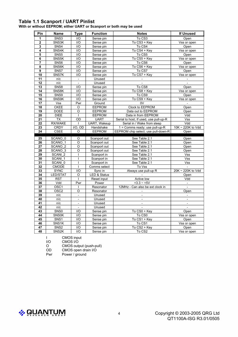
Table 1.1 Scanport / UART PinlistWith or without EEPROM; either UART or Scanport or both may be used
Vss or openTo CS2Sense pinI/OSNS2K48OpenTo CS2 + KeySense pinI/OSNS247
Vss or openTo CS1Sense pinI/OSNS1K46OpenTo CS1 + KeySense pinI/OSNS145
Vss or openTo CS0Sense pinI/OSNS0K44OpenTo CS0 + KeySense pinI/OSNS043
--Unused-n/c42--Unused-n/c41--Unused-n/c40--Unused-n/c39
Open-ResonatorOOSC238-12MHz - Can also be ext clock inResonatorIOSC137-+3.3 ~ +5VPowerPwrVdd36
VddActive lowReset inputIRST35Open-LED & StatusOLED/STAT34
20K ~ 220K to VddAlways use pull-up RSync inI/OSYNC33-To VssComms selectICMODE32
VssSee Table 2.1Scanport inISCANI_031VssSee Table 2.1Scanport inISCANI_130VssSee Table 2.1Scanport inISCANI_229
OpenSee Table 2.1Scanport outOSCANO_328OpenSee Table 2.1Scanport outOSCANO_227OpenSee Table 2.1Scanport outOSCANO_126OpenSee Table 2.1Scanport outOSCANO_025
OpenEEPROM chip select; use pull-down-REEPROMOCSEE2410K ~ 220K to Vdd1 = Comms ready; use pull-up-RHandshakeI/O, ODCRDY23
VddSerial in / Wake from sleepUART, WakeupIRX/WAKE22VssSerial to host; If used, use pull-up-R UARTODTX21VddData in from EEPROMEEPROMIDIEE20
OpenData out to EEPROMEEPROMODOEE19OpenClock to EEPROM EEPROMOCKEE18
-0VGroundPwrVss17Vss or openTo CS9 + KeySense pinI/OSNS9K16
OpenTo CS9Sense pinI/OSNS915Vss or openTo CS8 + KeySense pinI/OSNS8K14
OpenTo CS8Sense pinI/OSNS813--Unused-n/c12--Unused-n/c11
Vss or openTo CS7 + KeySense pinI/OSNS7K10OpenTo CS7Sense pinI/OSNS79
Vss or openTo CS6 + KeySense pinI/OSNS6K8OpenTo CS6Sense pinI/OSNS67
Vss or openTo CS5 + KeySense pinI/OSNS5K6OpenTo CS5Sense pinI/OSNS55
Vss or openTo CS4 + KeySense pinI/OSNS4K4OpenTo CS4Sense pinI/OSNS43
Vss or openTo CS3 + KeySense pinI/OSNS3K2OpenTo CS3Sense pinI/OSNS31
If UnusedNotesFunctionTypeNamePin
I CMOS inputI/O CMOS I/OO CMOS output (push-pull)OD CMOS open drain I/OPwr Power / ground
L Q 4 Copyright © 2003-2005 QRG LtdQT1100A-ISG R3.01/0505
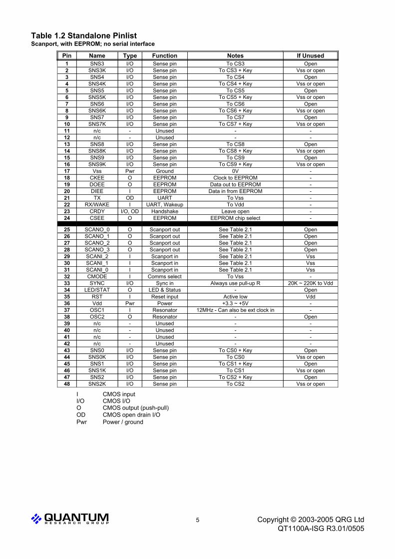
Table 1.2 Standalone PinlistScanport, with EEPROM; no serial interface
Vss or openTo CS2Sense pinI/OSNS2K48OpenTo CS2 + KeySense pinI/OSNS247
Vss or openTo CS1Sense pinI/OSNS1K46OpenTo CS1 + KeySense pinI/OSNS145
Vss or openTo CS0Sense pinI/OSNS0K44OpenTo CS0 + KeySense pinI/OSNS043
--Unused-n/c42--Unused-n/c41--Unused-n/c40--Unused-n/c39
Open-ResonatorOOSC238-12MHz - Can also be ext clock inResonatorIOSC137-+3.3 ~ +5VPowerPwrVdd36
VddActive lowReset inputIRST35Open-LED & StatusOLED/STAT34
20K ~ 220K to VddAlways use pull-up RSync inI/OSYNC33-To VssComms selectICMODE32
VssSee Table 2.1Scanport inISCANI_031VssSee Table 2.1Scanport inISCANI_130VssSee Table 2.1Scanport inISCANI_229
OpenSee Table 2.1Scanport outOSCANO_328OpenSee Table 2.1Scanport outOSCANO_227OpenSee Table 2.1Scanport outOSCANO_126OpenSee Table 2.1Scanport outOSCANO_025
-EEPROM chip selectEEPROMOCSEE24-Leave openHandshakeI/O, ODCRDY23-To VddUART, WakeupIRX/WAKE22-To VssUARTODTX21-Data in from EEPROMEEPROMIDIEE20-Data out to EEPROMEEPROMODOEE19-Clock to EEPROMEEPROMOCKEE18-0VGroundPwrVss17
Vss or openTo CS9 + KeySense pinI/OSNS9K16OpenTo CS9Sense pinI/OSNS915
Vss or openTo CS8 + KeySense pinI/OSNS8K14OpenTo CS8Sense pinI/OSNS813
--Unused-n/c12--Unused-n/c11
Vss or openTo CS7 + KeySense pinI/OSNS7K10OpenTo CS7Sense pinI/OSNS79
Vss or openTo CS6 + KeySense pinI/OSNS6K8OpenTo CS6Sense pinI/OSNS67
Vss or openTo CS5 + KeySense pinI/OSNS5K6OpenTo CS5Sense pinI/OSNS55
Vss or openTo CS4 + KeySense pinI/OSNS4K4OpenTo CS4Sense pinI/OSNS43
Vss or openTo CS3 + KeySense pinI/OSNS3K2OpenTo CS3Sense pinI/OSNS31
If UnusedNotesFunctionTypeNamePin
I CMOS inputI/O CMOS I/OO CMOS output (push-pull)OD CMOS open drain I/OPwr Power / ground
L Q 5 Copyright © 2003-2005 QRG LtdQT1100A-ISG R3.01/0505

Table 1.3 Standalone PinlistScanport, without EEPROM; no serial interface
Vss or openTo CS2Sense pinI/OSNS2K48OpenTo CS2 + KeySense pinI/OSNS247
Vss or openTo CS1Sense pinI/OSNS1K46OpenTo CS1 + KeySense pinI/OSNS145
Vss or openTo CS0Sense pinI/OSNS0K44OpenTo CS0 + KeySense pinI/OSNS043
--Unused-n/c42--Unused-n/c41--Unused-n/c40--Unused-n/c39
Open-ResonatorOOSC238-12MHz - Can also be ext clock inResonatorIOSC137-+3.3 ~ +5VPowerPwrVdd36
VddActive lowReset inputIRST35Open-LED & StatusOLED/STAT34
20K ~ 220K to VddAlways use pull-up RSync inI/OSYNC33-To VssComms selectICMODE32
VssSee Table 2.1Scanport inISCANI_031VssSee Table 2.1Scanport inISCANI_130VssSee Table 2.1Scanport inISCANI_229
OpenSee Table 2.1Scanport outOSCANO_328OpenSee Table 2.1Scanport outOSCANO_227OpenSee Table 2.1Scanport outOSCANO_126OpenSee Table 2.1Scanport outOSCANO_025
-OpenEEPROMOCSEE24-Leave openHandshakeI/O, ODCRDY23-To VddUART, WakeupIRX/WAKE22-To VssUARTODTX21-EEPROMIDIEE20-
Connect DOEE, DIEE togetherEEPROMODOEE19
-OpenEEPROMOCKEE18-0VGroundPwrVss17
Vss or openTo CS9 + KeySense pinI/OSNS9K16OpenTo CS9Sense pinI/OSNS915
Vss or openTo CS8 + KeySense pinI/OSNS8K14OpenTo CS8Sense pinI/OSNS813
--Unused-n/c12--Unused-n/c11
Vss or openTo CS7 + KeySense pinI/OSNS7K10OpenTo CS7Sense pinI/OSNS79
Vss or openTo CS6 + KeySense pinI/OSNS6K8OpenTo CS6Sense pinI/OSNS67
Vss or openTo CS5 + KeySense pinI/OSNS5K6OpenTo CS5Sense pinI/OSNS55
Vss or openTo CS4 + KeySense pinI/OSNS4K4OpenTo CS4Sense pinI/OSNS43
Vss or openTo CS3 + KeySense pinI/OSNS3K2OpenTo CS3Sense pinI/OSNS31
If UnusedNotesFunctionTypeNamePin
I CMOS inputI/O CMOS I/OO CMOS output (push-pull)OD CMOS open drain I/OPwr Power / ground
L Q 6 Copyright © 2003-2005 QRG LtdQT1100A-ISG R3.01/0505

Table 1.4 SPI PinlistWith or without EEPROM
Vss or openTo CS2Sense pinI/OSNS2K48OpenTo CS2 + KeySense pinI/OSNS247
Vss or openTo CS1Sense pinI/OSNS1K46OpenTo CS1 + KeySense pinI/OSNS145
Vss or openTo CS0Sense pinI/OSNS0K44OpenTo CS0 + KeySense pinI/OSNS043
--Unused-n/c42--Unused-n/c41--Unused-n/c40--Unused-n/c39
Open-ResonatorOOSC238-12MHz - Can also be ext clock inResonatorIOSC137-+3.3 ~ +5VPowerPwrVdd36
VddActive lowReset inputIRST35Open -LED & StatusOLED/STAT34
20K ~ 220K to VddAlways use pull-up RSync InI/OSYNC33-To VddComms selectICMODE32-To VssUnusedIn/c31-To VssUnusedIn/c30-From hostSPI Slave selectI/SS29-From hostSPI dataIDI28-To host; use pull-up RSPI dataI/ODO27-From hostSPI clockICLK26
Vss-unusedIn/c25
OpenEEPROM chip select; Use pull-down REEPROMOCSEE24-1 = Comms ready; Use pull-up RSPI handshakeODCRDY23
VddWake from sleepWakeIWAKE22-To VssUnused-n/c21
VddData in from EEPROMEEPROMIDIEE20OpenData out to EEPROMEEPROMODOEE19OpenClock to EEPROM EEPROMOCKEE18
-0VGroundPwrVss17Vss or openTo CS9 + KeySense pinI/OSNS9K16
OpenTo CS9Sense pinI/OSNS915Vss or openTo CS8 + KeySense pinI/OSNS8K14
OpenTo CS8Sense pinI/OSNS813--Unused-n/c12--Unused-n/c11
Vss or openTo CS7 + KeySense pinI/OSNS7K10OpenTo CS7Sense pinI/OSNS79
Vss or openTo CS6 + KeySense pinI/OSNS6K8OpenTo CS6Sense pinI/OSNS67
Vss or openTo CS5 + KeySense pinI/OSNS5K6OpenTo CS5Sense pinI/OSNS55
Vss or openTo CS4 + KeySense pinI/OSNS4K4OpenTo CS4Sense pinI/OSNS43
Vss or openTo CS3 + KeySense pinI/OSNS3K2OpenTo CS3Sense pinI/OSNS31
If UnusedNotesFunctionTypeNamePin
I CMOS inputI/O CMOS I/OO CMOS output (push-pull)OD CMOS open drain I/OPwr Power / ground
L Q 7 Copyright © 2003-2005 QRG LtdQT1100A-ISG R3.01/0505

Table 1.5 Pin Descriptions
Connect to 12MHz resonator; leave open if external clock is usedOSC2
Connect to 12MHz resonator; can also be an external clock inputOSC1
Reset input, low resets device. Normally this pin can be tied to Vdd, or driven froma host controller.
/RST
LED & Status output pin. This pin can sink 1mA to drive a status LED, or be usedby a host controller to determine device error condition or status .
LED/STAT
Sync Input to synchronize acquisitions to an external source or another QT chip.Always use a pull-up resistor on this pin.
SYNC
Communications mode select pin. For UART or scanport operation, connect toVss. For SPI mode, connect to Vdd.
CMODE
Input scan linesSCANI_x
Output scan linesSCANO_x
SPI Slave select from host/SS
SPI data in from hostDI
SPI data output to host. Always use a pull -up resistor on this pin.DO
SPI clock input from hostCLK
Chip select drive to serial EEPROM. Always use a pull-down resistor on this pin.CSEE
Serial interface handshake pin; bidirectional in UART mode, output only in SPImode. Always use a pull-up resistor on this pin.
CRDY
Receive pin in UART mode; alternately or in addition, Wake from sleep RX/WAKE
Serial port pin for UARTTX
Input data line, from serial EEPROMDIEE
Output data line, to serial EEPROMDOEE
Clock line output, to drive serial EEPROMCKEE
Sense pin, to Cs and to key electrodeSNSnK
Sense pin, to Cs reference capacitorSNSnDescriptionPin
L Q 8 Copyright © 2003-2005 QRG LtdQT1100A-ISG R3.01/0505
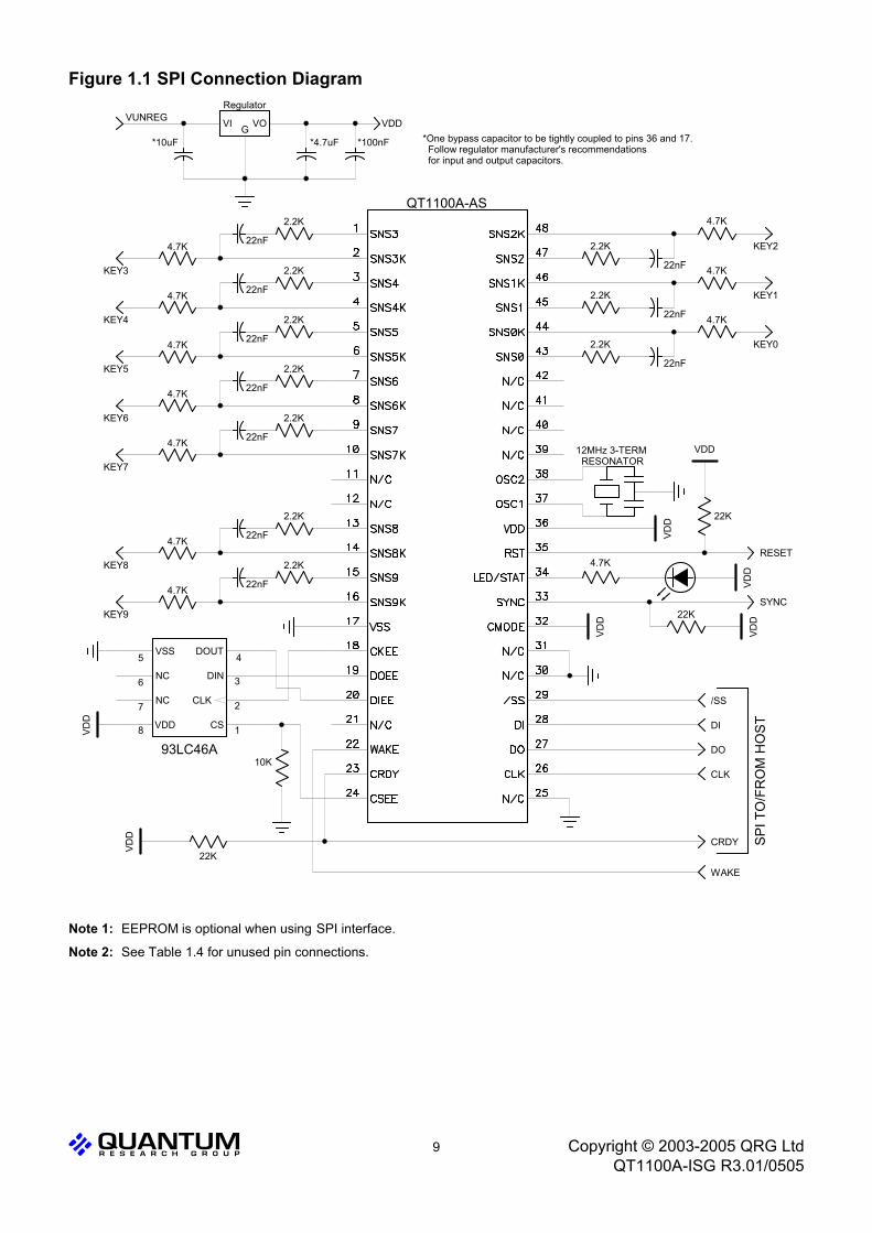
Figure 1.1 SPI Connection Diagram
DO
DI
VDD
CLK
/SS
SP
I TO
/FR
OM
HO
ST
VDD
KEY9
KEY7
KEY4
22nF
22nF
22nF
Regulator
QT1100A-AS
WAKE
CRDY
VDD
KEY2
KEY8
KEY6
KEY5
KEY3
VUNREG
*10uF
10K
2.2K
2.2K
2.2K
2.2K
2.2K
2.2K
22nF
2.2K
*4.7uF
4.7K
VDD
2.2K
2.2K
SYNC
VDD22K
VDD
4.7K
4.7K
KEY1
KEY0
4.7K
VDD
22nF
22nF
22nF
2.2K
22K
4.7K
22nF
93LC46A
4.7K
4.7K
4.7K
VI VOG*100nF
RESET
12MHz 3-TERM RESONATOR
22nF
22nF
22K
4.7K
4.7K
4.7K
2CLK
1CS
3DIN
4DOUT
7NC
6NC
5VSS
8 VDD
VDD
*One bypass capacitor to be tightly coupled to pins 36 and 17. Follow regulator manufacturer's recommendations for input and output capacitors.
Note 1: EEPROM is optional when using SPI interface.
Note 2: See Table 1.4 for unused pin connections.
L Q 9 Copyright © 2003-2005 QRG LtdQT1100A-ISG R3.01/0505
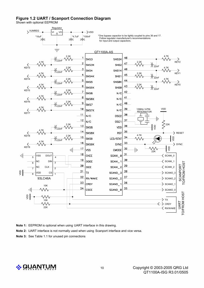
Figure 1.2 UART / Scanport Connection DiagramShown with optional EEPROM
TX
VDD
VDD
KEY9
KEY7
KEY4
22nF
22nF
22nF
Regulator
QT1100A-AS
RX/WAKE
CRDY
SCANO_0
SCANO_2
SCANO_3
SCANI_0
VDD
KEY2
KEY8
KEY6
KEY5
KEY3
VUNREG
*10uF
2.2K
2.2K
2.2K
2.2K
2.2K
2.2K
22nF
2.2K
*4.7uF
4.7K
2.2K
2.2K
SCANI_2
SCANO_1
SYNC
VDD
SCANI_1
VDD
4.7K
4.7K
KEY1
KEY0
4.7K
VDD
22nF
22nF
22nF
2.2K
22K
10K
4.7K
22nF
22K
10K
93LC46A
4.7K
4.7K
4.7K
VI VOG*100nF
RESET
22K
12MHz 3-PIN RESONATOR
22nF
22nF
4.7K
4.7K
4.7K
2CLK
1CS
3DIN
4DOUT
7NC
6NC
5VSS
8 VDD
UA
RT
TO/F
RO
M H
OS
T
VDD
S
CA
NP
OR
T TO
/FR
OM
HO
ST
*One bypass capacitor to be tightly coupled to pins 36 and 17. Follow regulator manufacturer's recommendations for input and output capacitors.
Note 1: EEPROM is optional when using UART interface in this drawing.
Note 2: UART interface is not normally used when using Scanport interface and vice versa.
Note 3: See Table 1.1 for unused pin connections
L Q 10 Copyright © 2003-2005 QRG LtdQT1100A-ISG R3.01/0505
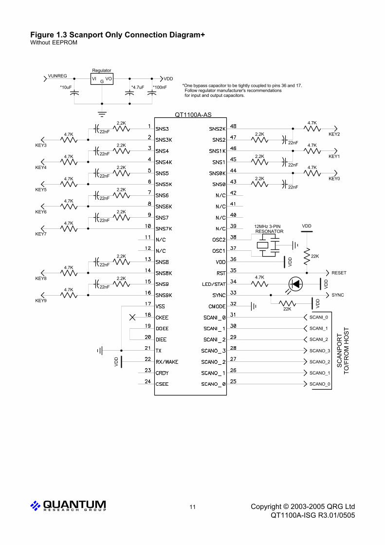
Figure 1.3 Scanport Only Connection Diagram+Without EEPROM
KEY9
KEY7
KEY4
22nF
22nF
22nF
Regulator
QT1100A-AS
SCANO_0
SCANO_2
SCANO_3
SCANI_0
VD
D
KEY2
KEY8
KEY6
KEY5
KEY3
VUNREG
*10uF
VD
D
2.2K
2.2K
2.2K
2.2K
2.2K
2.2K
22nF
2.2K
*4.7uF
VDD
*100nF
4.7K
2.2K
2.2K
SCANI_2
SCANO_1
SYNC
VD
D
SCANI_1
VDD
4.7K
4.7K
KEY1
KEY0
4.7K
22nF
22nF
22nF
2.2K
22K
4.7K
22nF
4.7K
4.7K
4.7K
VI VOG
RESET
22K
12MHz 3-PIN RESONATOR
22nF
22nF
*One bypass capacitor to be tightly coupled to pins 36 and 17. Follow regulator manufacturer's recommendations for input and output capacitors.
4.7K
4.7K
4.7K VD
D
S
CAN
POR
T TO
/FR
OM
HO
ST
L Q 11 Copyright © 2003-2005 QRG LtdQT1100A-ISG R3.01/0505

2 Device Control & Wiring2.1 OscillatorThe QT1100A uses an external 12MHz resonator as itsfrequency reference. This frequency can be lowered forlower average power, however all functions will also slowdown including response time and communicationsparameters. It is not advised to change the operatingfrequency without a good reason.
The oscillator source can be from an external circuit, so thattwo or more circuits can share the same oscillator. If anexternal frequency source is used, it should be fed to OSC1,pin 37. OSC2 should be left open-circuit.
2.2 Spread Spectrum ModulationThe device features spread spectrum modulation of itsacquisition bursts to dramatically reduce both RF emissionsand susceptibility to external AC fields. This feature cannotbe disabled or modified.
Spread spectrum modulation works together with thedetection integrator (‘DI’) process to eliminate externalinterference in almost all cases.
2.3 Cs Sample CapacitorsThe Cs sample capacitors accumulate the charge from thekey electrodes and determine sensitivity . (See Section 2.4)
The Cs capacitors can be virtually any plastic film or low tomedium-K ceramic capacitor. The ‘normal’ Cs range is 2.2nFto 100nF depending on the sensitivity required; larger valuesof Cs require higher stability to ensure reliable sensing.Acceptable capacitor types for most uses include PPS film,polypropylene film, and NP0 and X7R ceramics. Lowergrades than X7R are not advised.
The Cs capacitors and all associated wiring should beplaced and wired very tight to the body of the IC for noiseimmunity to very high frequency RF fields. See Section 2.7.
2.4 SensitivitySensitivity can be altered to suit various applications andsituations on a key-by-key basis. One way to impactsensitivity is to alter the value of each Cs when the device isin NTM = 0 mode (see page 25); higher values of Cs willyield higher sensitivity; each key has its own Cs value andso can be adjusted independently. The Setups block canalso be used to alter sensitivity, using an external EEPROM, serial communications, or both (Section 4.1).
Sensitivity can also be increased by using bigger electrodeareas, reducing panel thickness, or using a panel materialwith a higher dielectric constant (e.g. glass instead ofplastic).
In some cases the keys may be too sensitive. Gain ca n belowered by:
a) making the electrode smaller, or,
b) making the electrode into a sparse mesh using a highspace-to-conductor ratio, or,
c) by decreasing the Cs capacitors (if NTM = 0).
Sensitivity trimming is usually done through a process of trialand error, using a range of ‘standard fingers’ made ofearthed conductive rubber on the end of a plastic rod.
2.5 Sensitivity BalanceA number of factors can cause sensitivity imbalances amongthe keys. Notably, SNS wiring to electrodes can havediffering stray amounts of capacitance to ground, perhapsdue to trace length differences or the presence of ground,power, or other signal wiring near the SNS traces. Increasingload capacitance (Cx) will cause a decrease in gain. Keysize differences, and proximity to other metal surfaces canalso impact gain.
The keys may thus require ‘balancing’ to achieve similarsensitivity levels. The NTHR parameter in the Setupsfunctions is one easy way to trim and balance key sensitivity(Section 4.1).
Balancing can also be achieved by adjusting the Cscapacitor values to achieve equilibrium. The Rs resistorshave no effect on sensitivity and should not be altered. Loadcapacitance to ground (to boost Cx) can also be added tooverly sensitive channels to reduce gain; these should be onthe order of a few picofarads.
2.6 Power SupplyThe power supply can range from 3.3 to 5.0 volts. If thisfluctuates slowly with temperature, the device will track andcompensate for these changes automatically with only minorchanges in sensitivity. If the supply voltage drifts or shiftsquickly, the drift compensation mechanism will not be able tokeep up, causing sensitivity anomalies or false detections.
The power supply should be locally regulated using a3-terminal device. If the supply is shared with anotherelectronic system, care should be taken to ensure that thesupply is free of digital spikes, sags, and surges which cancause adverse effects.
For proper operation a 0.1µF or greater bypass capacitormust be used between Vdd and Vss; the bypass cap acitorshould be routed with very short tracks to the device’s Vssand Vdd pins.
2.7 PCB Layout and ConstructionGround Planes: The PCB should if possible include acopper pour under and around the IC, but not under the SNSlines after the Rsns resistors. Ground planes increaseloading capacitance (Cx) on the SNS lines and candramatically degrade sensitivity.
Part Placement: The resistors and capacitors associatedwith each key should be placed physically as close to thebody of the QT1100A as possible, with the shortest possibletrace lengths, to minimize the influence of external fields(see Section 2.9.2). The QT1100A should be placed as closeto the key electrodes as possible to reduce wiring lengths, tominimize stray capacitances on and between SNS tracesand to reduce interference problems.
PCB Cleanliness: All capacitive sensors should be treatedas highly sensitive analog circuits which can be influencedby stray conductive leakage paths. QT devices have a basicresolution in the femtofarad range; in this range, there is nosuch thing as ‘no-clean flux’. Flux absorbs moisture andbecomes conductive between solder joints, causing signaldrift, false detections, and transient instabilities. Conformalcoatings will trap in existing amounts of moisture which willthen become highly temperature sensitive.
The designer should specify ultrasonic cleaning as part ofthe manufacturing process, and in cases where a high levelof humidity is anticipated, the use of conformal coatings aftercleaning to keep out moisture.
L Q 12 Copyright © 2003-2005 QRG LtdQT1100A-ISG R3.01/0505
2.8 ESD ProtectionNormally, only a series resistor is required for ESDsuppression. A 10K to 22K Rsns resistor in series with eachsense trace to each key is normally sufficient. The dielectricpanel (glass or plastic) usually provides a high degree ofisolation to prevent ESD discharge from reaching the circuit.
The Rsns resistors should be placed close to and wiredtightly to the chip, not the keys.
If the Cx load is high, Rsns can prevent total charge andtransfer and as a result gain can deteriorate. If a reduction inRsns increases gain noticeably, the lower value should beused. Conversely, increasing the Rsns can result in addedESD and EMC benefits provided that the increase inresistance does not decrease sensitivity.
2.9 Noise Issues2.9.1 LED Traces and Other Switching SignalsDigital switching signals near the SNS lines will inducetransients into the acquired signals, deteriorating the SNRperformance of the device. Such signals should be routedaway from the SNS lines, or the design should be such thatthese lines are not switched during the course of signalacquisition (bursts).
LED terminals which are multiplexed or switched into afloating state and which are within or physically very near akey structure (even if on another nearby PCB) should bebypassed to either Vss or Vdd with at least a 10nF capacitorof any type, to suppress capacitive coupling effects whichcan induce false signal shifts. LED terminals which areconstantly connected to Vss or Vdd do not need bypassing.
2.9.2 External FieldsExternal AC fields (EMI) due to RF transmitters or electricalnoise sources can cause false detections or unexplainedshifts in sensitivity.
The influence of external fields on the sensor is reduced bymeans of the Rsns series resistors. The Cs capacitors andthe Rsns resistors form a natural low-pass filter for incomingRF signals; the roll-off frequency of this network is definedby -
FR = 12✜RSNSCS
If for example Cs = 4.7nF, and Rsns = 10K, the EMI rollofffrequency is ~3.4kHz, which is much lower than most noisesources (except for mains frequencies i.e. 50/60Hz).
Rsns and Cs must both be placed very close to the body ofthe IC so that the lead lengths between them and the IC donot form an unfiltered antenna at very high frequencies.
PCB layout, grounding, and the structure of the inputcircuitry have a great bearing on the success of a design towithstand electromagnetic fields and be relatively noise-free.
These design rules should be adhered to for best ESD andEMC results:
1. Use only SMT components.
2. Keep all Cs, Rs, Rsns, and the Vdd/Vss bypasscapacitor components wired tightly to the IC.
3. Place the QT1100A as close to the keys themselves aspossible.
4. Do not place electrodes or associated wiring nearother signals, or near a ground plane. If a ground planeis unavoidable, keep the SNS tracks very thin (e.g.
0.15mm) and relieve the ground plane widely aroundthem (e.g. 5mm clear space on all sides).
5. Do use a ground plane under and around the chipitself, back to the regulator and power connector (butnot beyond the Rs/Cs/Rsns networks).
6. To prevent cross interference, do not place anelectrode or SNS traces of one QT1100A near theelectrode or the SNS traces of another QT1100A orsimilar device, unless they are synchronized with aSync signal in a way that adjacent traces and keys donot have acquisition bursts on them at the same time.
7. Keep the electrodes (and wiring) away from othertraces carrying AC or switched signals.
8. If there are switched LEDs or related wiring near anelectrode or SNS traces (e.g. for backlighting of a key),bypass the switched traces to ground.
9. Use a voltage regulator just for the QT1100A toeliminate noise coupling from other switching sourcesvia Vdd. Make sure the regulator’s transient loadstability provides for a stable, settled voltage justbefore each burst commences.
2.10 Start-up TimeAfter a reset or power-up event, the device requires 400msto read the EEPROM, if one is connected, initialize thedevice, and start acquiring signals. After this time, the partwill calibrate all keys. The calibration time depends on theburst spacing but is about 450ms for a burst spacing of 3ms.This time is proportional to the burst spacing (Section 4.14).The burst spacing governs the time from the start of one keyacquisition cycle to the next, and can be set via serial Setupsor via the external EEPROM. Thus, the total start-up timeafter a reset is about 850ms if the burst spacing is set to3ms.
The device will communicate immediately after the Setupblock is loaded (from EEPROM. if any, or from defaults).
2.11 Operating Parameter SetupsThe device features a Setups block area in internal RAM thatholds numerous configuration parameters determin ing howthe part will operate. Each key can be configured individuallyfor a wide variety of parameters as discussed in Section 4. Inaddition, the device can be configured for the AKS™ functionwhich treats participating keys as a group in which only thekey with the strongest signal will generate a response.
Standalone (with EEPROM) Setups: In standalone modewith EEPROM, device setups are configured using anexternal 93LC46A byte-mode EEPROM (see Table 1.2, page5). This part can be programmed separately using acommercially obtainable programming device then insertedinto the circuit, or, it can be programmed using a QT1100A inserial mode via a PC interface with the 93LC46A in a socketso that it can be transferred to the target PCB.
The EEPROM contents and default values are detailed inTable 4-1, page 31. The last EEPROM entry should be aCRC check byte. If the CRC byte is set to 0xD6, the CRC willbe ignored.
In standalone mode the EEPROM must have the first byte inlocation 0 set to the value 0xD6 for the EEPROM to be read.The rest of the Setup table must follow, starting at location 1in the EEPROM.
L Q 13 Copyright © 2003-2005 QRG LtdQT1100A-ISG R3.01/0505

Without the EEPROM the QT1100A will operate in a defaultmode, designed to accommodate most touch sensingrequirements (Section 2.12, below).
Serial Mode Setups: The two serial interfaces permit ahost MCU to program control setups into the QT1100A onpower-up or even during normal operation, allowing low costreconfigurability. This is performed with a block of data,referred to as a Setups block.
The Setups block must end with a CRC check byte. If theoptional 93LC46A EEPROM is also used, the Setups blockwill be stored locally so that there is no need to reload aftereach power-up.
2.12 Standalone Operation, No EEPROMThe device can operate in Standalone Mode without serialcommunications or EEPROM using only its parallel scanportinterface. (See Table 1.3, page 6 and Figure 1.3, page11)
There are some minor differences in the default settings andbehaviour in Standalone Mode without EEPROM comparedwith other modes:
1. K2L is enabled on all keys*
2. SYNC is enabled (SE = 1)*
3. No serial comms - CRDY is always clamped low
*These exceptions are noted in Table 4-1, page 31.
2.13 EEPROM FunctionalityThe serial EEPROM is used to store Setups informationwhich alters the device behavior. If the EEPROM is not used,the device uses default parameters to operate , or,customized parameters loaded into the device via serialinterface.
The EEPROM’s functionality is not necessary when usedwith a serial interface. The host serial controller can send theSetups to the QT1100A following each power-up. In a serialmode, the EEPROM eliminates the need to send Setupsafter each power-up since they are stored locally.
The EEPROM must contain the value 0xD6 as its first byteor it will not be read. The table on page 31 shows thecontents required for this EEPROM. A CRC must beappended to the end of the EEPROM table, or, the CRC canbe replaced by a 0xD6 code, in which case no CRCchecking will be performed (not recommended except as adevelopment shortcut). A blank EEPROM will be programmed properly when the host sends a Setups block tothe device.
EEPROM corruption is automatically detected every 2seconds during normal run operation . If the EEPROM isfound to be corrupt or erased, the EEPROM error flag is setin the device status byte (command 0xC2); the EEPROMitself is not corrected. If the device is using serialcommunications, the host controller should reload theSetups and then reset the device.
If in a serial mode an EEPROM is not installed, pin DIEEshould be connected to Vdd.
2.14 Scanport Interface The scanport functions as a ‘legacy replacement’ for a matrixscanned XY keyboard. Single inputs (one-of-three) onScan_In lines result in a pattern of bits on Scan_out pinsdepending on the keys that are active. If no keys are activethe Scan_out pins remain inactive. See connection pinlists,Tables 1.1 and 1.2.
All logic on the scanport is ‘active high’ for both Scan_In andScan_Out. The scanport maps to the Scan_In and Scan_Outpins as per Table 2.1.
00Key 9Key 8Scan In 2Key 7Key 6Key 5Key 4Scan In 1Key 3Key 2Key 1Key 0Scan In 0
Scan Out3
Scan Out2
Scan Out1
Scan Out0
Table 2.1 - Scanport I/O Mapping
The scanport is enabled if the CMODE pin is strapped low.The UART is also enabled in this mode but it can be ignored ;if UART serial is not used, TX should be connected to Vss.
Scanport Latency: The latency of the scanport fromScan_In to Scan_Out is 120µs maximum. UART transfers donot affect this response time. Scanning software has to takethis delay into account, i.e. it should not expect theScan_Out pins to be stable until 120µs after setting theScan_In pins.
One easy way to use the scanport is to read the scanportbefore changing the Scan_In signals. Normally, Scan_Inshould be changed to a new state every 1 ~ 2ms. Fasterscanning than this will not result in a perceptibly fasterresponse time. Therefore, if the Scan_Out lines are readimmediately before changing the Scan_In signals, the hostcontroller will not have to wait for the 120µs scanport latency.
System Response Time: The setting of the two detectionintegrators (see Section 4.9) strongly affects the basicdevice response time. The host’s scan rate adds to this time.If the basic QT1100A response time is set to 80ms, and thehost completely scans the device every 50ms, the totalresponse time can be a very slow 130ms.
One way to maintain good response time while minimizinghost activity is to have the host monitor the LED/STAT pin,perhaps via interrupt, and service the scanport only when theLED/STAT pin becomes active. (See Section 4.8, page 27)
Sleep/Wake Function: Sleep/Wake can only be used inconjunction with a serial mode which sets the sleep state viaa command, and so Sleep is not possible in Scanport modewithout a serial interface.
Sync Mode with Scanport: Sync mode can be enabledusing an EEPROM having the correct Setups; Sync modealso works in standalone mode without an EEPROM (seealso Section 4.12). In Sync mode the acquire bursts aresynchronized to the external clock source; the scanport willoperate correctly while the device is waiting for a sync edge.
2.15 Start-up SequencingAfter power-up or reset the flag ‘Reset Occurred ’ will be set.The user can read this flag with command 0xC2. This flagcan be reset by issuing a ‘0xC2 0xC7’ command sequence.
If an EEPROM is installed and the EEPROM’s CRC does notmatch its contents, or the first byte is not 0xD6, the error flag“EEPROM Error” will be set. In this case, the default Setupsettings will be used but the EEPROM contents will stayunchanged.
2.16 Error Detection and ReportingA ‘major error’ is one where an enabled key signal fallsbelow LBLL (Section 4.13) or rises above a value of 4095, orwhere there is a CRC error in RAM or EEPROM Setups. The
L Q 14 Copyright © 2003-2005 QRG LtdQT1100A-ISG R3.01/0505

former can occur if the Cs capacitor fails or there is a shortin the SNS circuit; if this happens, the affected key is shutdown immediately and the key is switched off.
Keys that are intentionally disabled will not burst, and socannot show an error. In standalone mode with no EEPROMpresent (Scanport mode), keys are disabled by strapping theSNS pins to ‘unused’ settings (Table 1.1 page 4), and thiswill not generate a ‘major error’, unless the error occurs afterthe part has gone through power-up calibration successfullywithout detecting that the key is disabled via SNS pinconfiguration.
In any mode that uses an EEPROM or uses either UART orSPI communications, keys must be disabled by setting theNTHR parameter to zero for the key(s) (Section 4.1). If inEEPROM or serial mode a key is disabled via SNS pin wiringonly, it will be classified as a ‘major error’.
3 Serial OperationThere are two serial interfaces in the QT1100A: UART, andSPI.
UART provides a simple solution using well knownasynchronous signalling. Many MCUs contain UART orUSART blocks which are perfectly suited to this mode.MCUs without a UART hardware function can easily use afirmware UART function in most cases. The chief advantageof UART mode is wiring simplicity: only 3 wires, (TX, RX, andCRDY) are required.
SPI communications are based on the well knownsynchronous interface used extensively betweenmicrocontrollers and peripherals. The QT1100A usesslave-only SPI mode. This interface does not require anaccurate clock rate, and can operate faster than UARTmode. However, SPI operation requires 5 wires.
The host device always initiates communicationssequences; the QT1100A is incapable of chattering databack to the host. A command from the host to the QT1100Aalways ends in a one or more byte response from theQT1100A. Some transmission types from the host requirethe use of a CRC check byte to provide for robustcommunications. This command/response design isintentional for FMEA purposes so that the host always hastotal control over the communications with the QT1100A.Effectively this behavior forces designs to have inherentlyself-checking ‘loop back’ characteristics.
System Response Time: The setting of the two detectionintegrators (see Section 4.9) strongly affects the basicdevice response time. The serial poll rate adds to thisresponse time. If the basic QT1100A response time is 80ms,and the host polls the device every 50ms, the total responsetime can be a very slow 130ms. Normally, the host shouldpoll the QT1100A every ~10ms to minimize delay ‘stacking’.To minimize delays further, the command 0xC9 can be used(‘Quick 1st Key’; see Section 3.5.14) instead of 0xC0.
One way to improve speed while minimizing host activity isto have the host monitor the LED/STAT pin, perhaps viainterrupt, and service the device with a 0xC0 or 0xC9command only when the LED/STAT pin becomes active.(See Section 4.8)
3.1 UART InterfaceUART mode allows a host device to communicateconveniently over two serial wires asynchronously, with ahandshaking line (CRDY) to provide bidirectional data flow
control. The UART mode operates in the same way and withthe same protocol and commands as the SPI interface.
UART mode is selected by strapping the CMODE pin low.UART mode and Scanport mode can operate together. Ifonly UART mode is desired, the Scan_In pins need to begrounded. If only the Scanport is used, the UART can beignored. An unused RX line should be connected directly toVdd.
UART transmission parameters are (Fosc = 12MHz):
Baud rate options: 4800, 9600, 19.2K, 28.8KStart bits: 1Data bits: 8Parity: NoneStop bits: 1
UART Operation with Scanport: Scanport and UARToperation can be used together. (See Section 2.14)
3.1.1 TX PinThe TX pin has an open-drain drive to allow bussing withother similar parts. The TX line can thus be shared with otherUART based peripherals such as a second QT1100A.
TX must be pulled high to Vdd with a resistor in UART mode.The resistor value will depend on the total amount of straycapacitance on TX - more capacitance will require lowervalues of pull-up resistor, especially at higher Baud rates.The risetime of the signals on this line should be 1/10th ofthe bit width, i.e., if running at 9600 Baud, the bit width isabout 100µs, and the risetime should be 10µs or less. Inmost cases, a 47K resistor is low enough, however thisshould be confirmed using an oscilloscope.
An unused TX pin should be connected to Vss.
3.1.2 Sleep/Wake Operation in UART ModeThe device can be put into sleep mode with a serialcommand (0x05). The device can sleep for up to 700ms;some time after this it will self-reset. The Wake and RXfunctions are on the same pin, which allows a host toconveniently wake the device with a dummy character (e.g.0x00 null) before communicating with it. Wake operates onthe falling edge; the negative-going level must be at least40µs wide to be recognized.
See also Section 3.4.6.
3.1.3 CRDY Operation in UART Mode The CRDY serial handshake pin is open-drain and requires a10K ~ 220K pull-up to Vdd. Either the host or the QT1100Acan pull down on this line to stop data flow (wired-ANDlogic). If CRDY is high the communications can flow in eitherdirection. The host should obey this control line or overrunsand transmission errors will occur in the device.
Host-to-QT1100A UART CRDY Behavior: If the CRDY lineis released by the host but the CRDY line stays low, thismeans the QT1100A is busy and cannot acceptcommunications. The host must wait for the CRDY line tofloat high again before it can send the byte. If the CRDY linehappens to go low again just as the host is about to send abyte, the host has a 10µs grace period in which it can stillinitiate the transmission. This is acceptable for most MCUtypes, however even fast PCs operating under Windowshave a difficult time responding within the 10µs grace periodand this can result in frequent transmission errors.
QT1100A-to-Host UART CRDY Behavior: When theQT1100A needs to send data back to the host, it will releasethe CRDY line (if not already released) and wait for it to float
L Q 15 Copyright © 2003-2005 QRG LtdQT1100A-ISG R3.01/0505

high before sending a byte. If the host is busy and cannotaccept data, it should clamp CRDY low until it is ready.Before each return byte is sent, the QT1100A will checkCRDY in this manner and wait until the host is ready beforesending.
The host should allow a 10µs grace period in which it canstill accept data from the QT1100A after it releases CRDYhigh, to allow for any delays in the response from the sensor.
CRDY / Burst Behavior: The pacing of CRDY and thetransmission of UART data are interleaved with acquisitionbursts. The QT1100A cannot send or receive data during aburst or for a short time thereafter. CRDY is forced low bythe QT1100A when a burst is taking place andcommunication is not possible. At the fastest burst spacing,there is at least a 250µs window of time between burstswhen communications can take place and CRDY is high.
If a serial transmission from QT1100A to host is occurringwhen a burst should be starting, the communications takesprecedence and the next acquisition burst is delayed.
3.2 SPI OperationRefer to page 38 for timing diagram.
The SPI mode allows a host device to communicateconveniently using four control lines synchronously, with aCRDY handshaking line to provide control flow. The SPImode operates in the same way and with the same protocoland commands as the UART interface. However whereasthe UART mode permits the QT1100A to send backresponses to the host under its own volition, the SPI mode isa slave mode only requiring the host to always generate theshift clock.
Where a response is expected back from the QT1100A, thehost can shift over a dummy null (0x00) command to theQT1100A which will be ignored. However the host can alsouse the opportunity to send over a new command to theQT1100A provided the new command is sent to theQT1100A during the shift out of the last response byte fromthe prior command. Thus, if there are two expectedresponse bytes to a command, the host can send and shiftback the following bytes:
Response_2 to ACommand_B3Response_1 to ANull2Response to prior command?Command_A1QT1100A ResponseHostShift #
However the following sequence is also acceptable, albeitmore wasteful of transmissions:
0x55 (see below*)Command_B4Response_2 to ANull3Response_1 to ANull2Response to prior command?Command_A1QT1100A ResponseHostShift #
The following will not work:
Response_2 to ACommand_C3Response_1 to ACommand_B2Response to prior command?Command_A1QT1100A ResponseHostShift #
In the last case, Command_B will be ignored and onlyCommand_A and Command_C will be recognized.
SPI transmission parameters are (Fosc = 12MHz):
Transmission mode: Slave-onlyClock rate: 100kHz maxClock duty cycle: 50%Data bits: 8Clock idle: HighClock shift out edge: FallingClock shift in edge: RisingDelay from shift in edge: None
*Note that the QT1100A returns a 0x55 dummy byte if itsoutput buffer has nothing else it can send.
3.2.1 Multi-Drop SPI CapabilityIn SPI mode the DO pin floats while /SS is high to allow theSPI lines to be shared with other devices. A 10K ~ 20K Ohmpull-up resistor should be used on this pin to prevent DOfrom freely floating.
When used with other similar devices, each QT1100A partshould have its own /SS and CRDY connections back to thehost controller; the other SPI lines can all be shared.
3.2.2 Sleep/Wake Operation in SPI ModeThe device can be put into sleep mode with a serialcommand (0x05). The device can sleep for up to 700ms;some time after this it will self-reset. Wake operates on thefalling edge; the negative-going level must be at least 40µswide to be recognized.
The Wake pin can be connected to /SS, and the host canthen wake the device from sleep using a >40µs negativedummy pulse on /SS.
See also Section 3.4.6.
3.2.3 CRDY Operation in SPI ModeCRDY is an open-drain line requiring a 10K ~ 220K Ohmpull-up resistor. The QT1100A will pull down on this line tostop data flow from the host. The QT1100A does notrespond to the host pulling CRDY low in SPI mode, since thehost is always in control of all data transmissions. CRDY isunidirectional (QT1100A to Host) in SPI mode.
The host must wait for CRDY to float high before it can clockthe SPI interface. If CRDY happens to go low again just asthe host is about to clock data, the host has a 10µs graceperiod in which it can still initiate /SS (slave select) eventhough CRDY has already gone low.
CRDY / Burst Behavior: The pacing of CRDY and thetransmission of UART data are interleaved with acquisitionbursts. The QT1100A cannot send or receive data during aburst or for a short time thereafter.
CRDY is forced low by the QT1100A when a burst is takingplace and communication is not possible. At the fastest burstspacing, there is at least a 250µs window of time betweenbursts when communications can take place and CRDY ishigh. Similarly, if the burst duration exceeds its timeslot, thedevice will ensure that there is an additional 250µsappended to the burst to allow for communications.
If a serial transmission is occurring when a burst should bestarting, the communication takes precedence and the nextacquisition burst is delayed. Therefore, the 250µs should beviewed as a minimum which can expand to meet the needsof a single byte transmission. Additional bytes will usuallyoccur in the next timeslot.
L Q 16 Copyright © 2003-2005 QRG LtdQT1100A-ISG R3.01/0505

3.3 Communication Error HandlingIf a communications error takes place, the host shouldrecover by issuing a ‘Return Last Command’ command(0xC7) at least twice to make sure the QT1100A and hostare communicating properly with each other.
3.4 Control CommandsControl commands are used to place the device into specialmodes or cause the device to reset, calibrate or run. (Seesummary Table 3-1, page 23)
3.4.1 Null Command - 0x00This command is used primarily to shift back data from theQT1100A in SPI mode.
Since the host device is always the master in SPI mode, anddata are clocked in both directions, the null command isrequired frequently to act as a placeholder where therequirement is only to get data back from the QT1100A, notto send data to it. See also Section 3.2.
In UART mode there is no response whatsoever to a nullcommand.
3.4.2 Enter Setups Load Mode - 0x01This command is used to load the Setups block into thedevice over either serial interface. See Table 4-1 on page 31for reference.
The command must be repeated 2 times within 100ms or thecommand will be aborted (not reset); the repeat of thecommand must be sequential without any other interveningcommand or even a null.
250µs worst case after receipt of the second 0x01, thedevice will start to send back the response byte 0x53(signalled using CRDY as always, i.e. the response could bedelayed beyond 250µs by the host itself, either via a lateshift operation in SPI Mode or via holding CRDY low inUART mode).
If no 0x53 is returned, the command was not properlyreceived; the host should recover by issuing a ‘Return LastCommand’ command (0xC7) at least twice to make sure theQT1100A and host are communicating properly with eachother, and then the 0x01 commands should be sent again.
From this point on the host should send the Setups blockincluding the ending CRC byte as a stream to the QT1100A,without interruption, paced only by the CRDY line. Duringthis time the chip suspends its normal acquisition bursts.The time between bytes can be from 10µs to a limit of100ms.
If a data timeout occurred in the block load (the timebetween any two sequential block data bytes exceeded100ms) a response of 0xF1 will immediately be attemptedback to the host, the Setup block sequence will be aborted,and the chip will reload the Setup block from the EEPROM(if available and correct) or from ‘factory defaults’. A devicereset will automatically occur if the QT1100A does notreceive a further command (any of 0x01, 0x02, 0x03 or0x04) within 1s after the block sequence has suspended dueto a timeout error.
The host should listen for a 0xF1 response while shifting theSetups block to terminate and restart the Setups loadsequence if required.
Note that in SPI mode, all responses must be shifted outwith nulls shifted over by the host.
EEPROM not present: If no EEPROM is installed and DIEEis tied to Vdd, the QT1100A will check the CRC and replywith a response byte:
0xF0 - CRC not OK, and as a result block load failed0xF1 - transfer timeout; time between bytes >100ms0xFE - block loaded OK, CRC is OK
In the case of either 0xF0 or 0xF1, the QT1100A will load‘factory defaults’ into the device (when no EEPROM ispresent).
With no EEPROM present, the delay between the CRC bytesent to the QT1100A and the response back from theQT1100A is 800µs maximum (signalled using CRDY).
EEPROM present: With an EEPROM installed, the devicewill check the CRC and if valid, start programming theEEPROM with the new Setup block, and check that theEEPROM is written correctly. It will respond as follows:
0xF0 - CRC is not OK, and as a result block load failed0xF1 - transfer timeout; time between bytes >100ms0xF2 - block loaded OK, but EEPROM write failed0xFE - block loaded OK, CRC is OK, EEPROM write OK
(0xFE response requires up to 370ms due toEEPROM write time - this is dependent largely on theEEPROM’s write time specification)
If there is no response from the device within 370ms afterthe block has been completely sent , the command was notproperly received and the device should preferably be resetusing the RST pin before attempting the command again.
Only if the entire Setup block is received without error andthe CRC is OK (or 0xD6 for testing; see below) will theSetups information be recorded to EEPROM.
At the end of the full command sequence the device remainssuspended (acquire bursts are stopped) until a Setups, Run,Cal, or Reset command is received (0x01, 0x02, 0x03, or0x04). If one of these commands is not received within 1safter the block is loaded and the response byte is generated ,the part resets itself, enters Cal mode, and then runsautomatically.
If there was an error in the Setups load operation, the devicewill run either with ‘factory defaults’ (if there was a 0xF2error) or with previously stored EEPROM data (if there was a0XF0 or 0xF1 error).
CRC Note: The 0x01 command requires that the endingCRC byte is calculated by the host on the data block itselfwithout the 0x01 command itself being folded in to the CRC.This is a notable exception to the use of CRCs in this device.Other commands ending in a CRC fold in the command byteitself as the first byte in the CRC calculation.
Dummy CRC for Testing: For testing purposes, a dummyCRC byte, of value 0xD6, can be placed at the end of theSetups block which is always accepted by the QT1100Aeven though it is ‘wrong’. While a 0xD6 value will inhibit CRCchecking, the QT1100A will actually compute and record thecorrect CRC value into the EEPROM (if present).
Should an actual CRC calculation result in a 0xD6(probability = 0.39%) and CRC checking is required, thedesigner should change one of the unused bits shown in theSetup table (page 31) to cause the CRC to be somethingelse.
After a Setups Load: After a successful Setups block load,there are four basic options:
1. Run the device via the 0x02 command, i.e. without thebenefit of a recalibration, or,
L Q 17 Copyright © 2003-2005 QRG LtdQT1100A-ISG R3.01/0505

2. Calibrate the device via the 0x03 command, in whichcase the device will calibrate all keys and run again, or,
3. Reset the device using the 0x04 command, or,
4. Wait 1 second for the device to enter self-reset.
Changes to NDCR, NRD, AKS, EK, K2L, PDCR, PRD,PTHR, PHYS, LEDP, LBLL, KEYO, BR or BS do not requirea recalibration to take effect, and it is faster to just issue a0x02 RUN command after the 0x01 is complete.
Changes to NTHR, NHYS, NDIL, FDIL, and NTM should befollowed with a 0x03 Cal command.
Changes to SE or SYNC should be followed with a devicereset command, RST pin reset, or 1s timeout reset to allowthe new parameters to properly take effect.
3.4.3 Enter Run Mode - 0x02This command is used only after a Setups Load command(0x01) has completed to get the device to run as a sensor,without any key calibration. This is useful to make runningchanges, for example in drift compensation rates orthreshold levels, without disturbing key calibrations.
The command must be repeated 2 times within 100ms or thecommand will fail; the repeated command must besequential without any intervening command , not even anull. After the second 0x02, the QT1100A will reply with thecharacter 0xFD when the part begins to run as a sensor. Thedelay in responding to the second 0x02 with 0xFD is 250µsmaximum (signalled using CRDY).
If no 0xFD is returned, the command was not properlyreceived; the host should recover by issuing a ‘Return LastCommand’ command (0xC7) at least twice to make sure theQT1100A and host are communicating properly with eachother, and then the 0x02 commands should be sent again.
3.4.4 Enter Cal Mode - 0x03This command is normally used only after a Setups Loadcommand (0x01) has completed to get the entire device tocalibrate and run as a sensor. Note that on normal power-upor reset, the device will automatically enter Cal moderegardless, and then run normally. Therefore the only timethis command is required is when the part is suspendedafter a Setups load, or, if there is a need to recalibrate allkeys at one time during normal running.
The 0x1k command is more efficient for recalibratingindividual stuck keys if desired (Section 3.4.7).
The 0x03 command must be repeated 2 times within 100msor the command will fail; the repeating command must besequential without any intervening command , not even anull. After the second 0x03 from the host, the QT1100A willreply with the character 0xFC within 450µs if the commandhas been accepted. After the 0xFC response, the device willinitiate calibration of all keys in parallel.
The host can check the progress of calibration by issuing a0x8k command on the highest enabled key (e.g. key #9); allthe keys being calibrated by 0x03 will have finishedcalibrating when the highest key number is done.
The time required to calibrate all 10 keys is 15 completeacquire cycles, or 15 x 10 keys = 150 timeslots. If the burstspacing is 4ms, then Cal will require 600ms to calibrate all10 keys. Disabled keys do not reduce this time.
Afterwards, the host can check error flags to find whichkey(s) failed during calibration, if any, for example usingcommand 0xC2 (Section 3.5.7) or 0xC5 (Section 3.5.10).
This might happen if there is a component failure , short oropen circuit on the PCB.
If no 0xFC is returned, the command was not properlyreceived; the host should recover by issuing a ‘Return LastCommand’ command (0xC7) at least twice to make sure theQT1100A and host are communicating properly with eachother, and then the 0x03 commands should be sent again.
3.4.5 Force Reset - 0x04This command is used to cause the part to reset, in thesame way as a hardware /RST signal.
This command must be repeated 2 times within 100ms orthe command will fail; the repeating command must besequential without any intervening command , not even anull. After the second 0x04 from the host, the QT1100A willreply with the character 0xFB within 250µs to indicate that ithas been properly received.
If no 0xFB is returned, the command was not properlyreceived; the host should recover by issuing a ‘Return LastCommand’ command (0xC7) at least twice to make sure theQT1100A and host are communicating properly with eachother, and then the 0x04 commands should be sent again.
After the part resumes operation, it will set the “ResetOccurred” flag (see Section 2.15) to indicate there was apower-up event, and it will go through a complete Cal modeautomatically and then run and sense keys normally.
The device will calibrate and run after a delay of 100ms +150 burst spacings, which could be up to 1.05s on 7ms burstspacings. While calibrating, the QT1100A can communicateserially and the user can track the progress of ongoingcalibrations using command 0x8k.
3.4.6 Sleep - 0x05This command is useful to allow low average operatingpower when in standby mode or when fast response time isnot required. During sleep, the device consumes only a fewmicroamps of current. Using Sleep mode, it is possible to getaverage current consumption down to 100µA while havingthe part run with reduced response time. Actual averagecurrent drain will be a function of the ratio of running time tosleep time.
The 0x05 command must be repeated 2 times within 100msor the command will fail. After the second 0x05 from thehost, the device will reply with the character 0xFA within250µs. The device will then enter a Sleep mode untilawakened by a negative edge or negative pulse on theWAKE pin (pin 22), at least 40µs, wide or via a hardwarereset on the RST pin. Note that if the device is reset, it willrecalibrate on power-up, which is usually not desirable. If thedevice wakes via the WAKE pin, it will resume operation inthe same state from which it went to sleep.
If no 0xFA is returned, the command was not properlyreceived; the host should recover by issuing a ‘Return LastCommand’ command (0xC7) at least twice to make sure theQT1100A and host are communicating properly with eachother, and then the 0x04 commands should be sent again.
If the device is not awakened intentionally within 700ms ofentering sleep, the device can go into self-reset causing theinternal states and data to be lost , and a recalibration to beperformed.
In UART mode, the QT1100A can be awakened with a NULL(0x00) byte. In SPI mode, the QT1100A can be awakened byconnecting pin /SS to WAKE and sending an empty /SSpulse from the host to the QT.
L Q 18 Copyright © 2003-2005 QRG LtdQT1100A-ISG R3.01/0505

Wake time: The device requires ~160uS from the WAKEinput to resumption of normal sensing and communications.
3.4.7 Cal Key ‘k’ - 0x1kCalibrates only key k, where k = {0..9}. Example: Thecommand 0x14 causes key 4 to calibrate. This commandfunctions the same as the 0x03 Cal command (Section3.4.4, above) except this command only affects one key .
This command must be repeated 2 times within 100ms orthe command will fail; the repeating command must besequential without any intervening command , not even anull.
0x1k returns 0xF8 if the command has been accepted andwill be processed. This response can come up to one bursttimeslot after the second 0xF8 has been received. The usercan then track the progress of the key calibration with the0x8k command (Section 3.5.4).
If no 0xF8 is returned, the command was not properlyreceived; the host should recover by issuing a ‘Return LastCommand’ command (0xC7) at least twice to make sure theQT1100A and host are communicating properly with eachother, and then the 0x1k command should be sent again.
The chosen key ‘k’ is recalibrated in its normal bursttimeslot; normal running of the part is not interrupted and allother keys operate correctly throughout. This command is foruse only during normal operation to try to recover a singlekey that is stuck or has not calibrated correctly.
It is possible to issue several 0x1k commands to severalkeys sequentially, however the 0xF8 return value should bereceived back from a prior 0x1k command before a new0x1k command is issued.
3.5 Status CommandsStatus commands are used to evoke a response from theQT1100A, for example to return signal values or to get keystatus. See summary Table 3-2 on page 24.
3.5.1 Signal for 1 Key - 0x2kReturns the raw signal for key k, where k = {0..9}. Example:The command 0x25 addresses key 5. The value is a 16-bitnumber and no CRC is appended to the return, so the returndata should not be considered secure under FMEA rules.The valid return number range is from 0..4095. The high byteis returned first.
3.5.2 Reference for Key ‘k’ - 0x4kReturns the reference level for key k, where k = {0..9}.Example: The command 0x48 addresses key 8. The value isa 16-bit number and no CRC is appended to the return, sothe return data should not be considered secure underFMEA rules. The valid return number range is from 0..4095.The high byte is returned first.
3.5.3 Detect Integrator for Key ‘k’ - 0x6kReturns the detect ‘normal’ detect integrator (‘DI’) for key k,where k = {0..9}. Example: The command 0x63 addresseskey 3. The value is contained in the lower 4 bits of an 8-bitcharacter, i.e. in the range from 0..15; no CRC is appendedto the response, so the return data should not be consideredsecure under FMEA rules.
3.5.4 Status for Key ‘k’ - 0x8kReturns the status bits for key k, where k = {0..9}. Example:The command 0x87 addresses key 7. The return value iscontained in a single 8-bit character. A CRC is appended to
the return; this CRC includes the command 0x8k itself as thefirst byte in the CRC calculation.
The return bits are as follows:
1 = This key is disabled dueto a Setup configuration ordue to an extreme condition(non-volatile)
0
1 = This key is experiencingextreme signal conditions(non-volatile)
1
1 = This key has a cal error(non-volatile)
2
1 = This key is undergoingcalibration (volatile)
3
1 = This key is in process ofdetection (but not yet reportedas having detected) (volatile)
4unused5unused6
1 = This key is in detect(volatile)
7DescriptionBit #
Bit_7: 1 = Active key. The key is indicating a confirmedtouch. This bit is set or cleared dynamically depending onthe state of the DI counter for each key. This bit is willself-clear when touch is no longer detected.
Bit_4: 1 = Detection pending. The key is in the process oftrying to confirm a detection (the signal is below NTHR),but has not yet reported as active. Normally this flag isonly used for test purposes. This bit will self-clear whenthe key falls out of this state.
Bit_3: 1 = Calibration in progress. The key is in theprocess of calibration. This bit will self-clear when thecalibration is complete.
Bit_2: 1 = Cal error. There was an error on this key the lasttime it attempted a calibration. This means an overflow(signal >4095) or underflow (see Section 4.13, page 29)occurred during a cal cycle for that key. This bit isdetermined only after a Cal of the key in question (eithervia Cal 0x03 or 0x1k commands). After Reset, these bitsare cleared for all 10 keys and are set (or not) after thesubsequent Cal of the key(s) in question.
Bit_2 is non-volatile and can only be cleared byrecalibration or a device reset. Note that keys with faultycalibration stop operating and the correspondingacquisition bursts are disabled.
Bit_1: 1 = Extreme signal. The signal level currently on thiskey is either too high or too low for normal operation, i .e.if the real-time signal falls below the minimum signal leveldefined by LBLL (see Section 4.13, page 29), or if {signal>4095} counts.
Bit_1 is non-volatile, that is, the bit will remain '1' even ifthe problem is removed, until the key is recalibrated orthe device is reset. A key with Bit 1= 1 is automaticallydisabled and its acquisition burst is disabled.
This type of error may occur because the key either lacksa working Rs/Cs circuit or there is a short or open circuit.
Bit_0: 1 = Key disabled. This can be due to an intentionalSetups disable (NTHR Setup in the Setup block is set to0) or, there is a problem with the SNS pins (see Bit_1above).
This bit is persistent (non-volatile) and will not clearunless the key is re-enabled via a new Setups block load.
L Q 19 Copyright © 2003-2005 QRG LtdQT1100A-ISG R3.01/0505

3.5.5 Report 1st Key - 0xC0Reports the first or only key to be touched, plus indicates ifthere are yet other keys that are also touched.
The return bits are as follows:
Key bit 00Key bit 11Key bit 22Key bit 33# keys in detection, low bit4# keys in detection, high bit5Reserved: Can report 0 or 16Logical-OR of all error types7DescriptionBit #
Bit_7: 1 = Indicates if there are any errors anywhere in thepart, of any type.
Bits_4,5: Encode for the number of keys in detection: 01 = one key10 = two keys11 = 3 keys or more
Bits_0..3: Encode for the first detected key in range 0..9.
If there are 2 or more keys in detection, the host controllershould also interrogate the part via the 0xC1 command toread out all key detections. 0xC0 should be the dominantinterrogation command in the host interface; furthercommands like 0xC1, 0xC2, 0xC5 etc. can be issued if theresponse to 0xC0 warrants it.
A CRC byte is appended to the response; this CRC includesthe command 0xC0 itself as the first byte in the CRCcalculation.
See also the very similar 0xC9 command, page 21.
3.5.6 Report All Keys - 0xC1Returns two bytes which indicate any and all keys indetection, as a bitfield, one bit per key. The first bytereturned is the MSByte. Key 0 reports in LSByte bit 0. Key 9is reported in MSByte bit 1. The valid range of reporting isfrom 0..0x03FF (i.e. the bottom 10 bits).
A CRC byte is appended to the response; this CRC includesthe command 0xC1 itself as the first byte in the CRCcalculation.
3.5.7 Device Status - 0xC2This command returns a byte response which indicates thegeneral device status. The return bit flags of the byte are asfollows:
1 = Cal error(s) (non-volatile) *01 = CRC error in RAM (non-volatile) *11 = CRC error in EEPROM (non-volatile) *21 = Sync error (non-volatile)3
1 = Extreme signal on one or more keys(non-volatile) *
41 = Reset occurred (non-volatile)51 = Eeprom error (non-volatile)61 = Key(s) are detecting (volatile)7DescriptionBit #
*These error types are considered major errors and willcause a forced output on a chosen key or keys if EK mode isset (Section 4.7). In Standalone mode (only scanport activeand no EEPROM present), an extreme signal on a keydisables the key and is not considered a major error.
Bit_7 = 1: Keys Active. There are one or more keys indetection. This bit self-clears when there are no keys indetection.
Bit_6 = 1: EEPROM error. EEPROM is not attached, orEEPROM first byte is not 0xD6, or, the CRC of theEEPROM’s Setup block is not correct. If the EEPROM isabsent and DIEE is connected to Vdd, an error will bereported in this bit. This bit can be reset only by a devicereset or by the serial command sequence ‘0xC2 0xC7’.See note below.
Bit_5 = 1: Reset occurred. A reset event occurred. The bitcan only be reset by the sequence ‘0xC2 0xC7’. See notebelow.
Bit_4 = 1: Extreme signals. There are one or more keyswith an out-of-bounds signal condition. This bit is thelogical-OR of all 10 error flags from 0x8k bit 1 (extremesignal error). The bit can be reset only by a device resetor by a successful key recalibration.
Bit_3 = 1: Sync error. There has been a sync error, i.e. async pulse was not found for ~1s or more. If the syncpulses are restored, this error bit is NOT automaticallycleared. The bit can be reset only by device reset or bythe sequence ‘0xC2 0xC7’. See note below.
Bit_2 = 1: CRC EEPROM error. There has been a CRCerror in EEPROM (if an EEPROM is installed). This iscomputed approximately once per second. The bit can bereset only by device reset or by the sequence ‘0xC20xC7’. See note below.
Bit_1 = 1: CRC RAM error. There has been a CRC error inRAM. This is computed approximately once per second.The bit can be reset only by device reset or by thesequence ‘0xC2 0xC7’. See note below.
Bit_0 = 1: Cal error(s). There was at least one calibrationerror during the last calibration event. This bit is thelogical-OR of all 10 bit_2 error flags readable viacommand 0x8k (Cal error; see Section 3.5.4). Bit_0 iscleared only when all the Cal errors are cleared, whichcan happen only if the problem key(s) have beenrecalibrated properly.
A CRC byte is appended to the response; this CRCincludes the command 0xC2 itself as the first byte in theCRC calculation.
Note: The 0xC7 used to clear flag bits can immediatelyfollow the 0xC2 command; it is not required to issue the0xC2 command a second time before issuing the 0xC7.
3.5.8 EEPROM CRC - 0xC3This command returns the 8-bit CRC calculated from theEEPROM contents (if one is installed). The CRC iscalculated according to the algorithm shown in Section 6.
A CRC byte is appended to the response; this CRC includesthe command 0xC3 itself as the first byte in the CRCcalculation.
If this CRC does not agree with the expected result, thedevice should be reloaded with the Setups command (0x01).
If an EEPROM does not exist (and pin DIEE is tied to Vdd asrecommended) the returned value will be 0x00.
3.5.9 RAM CRC - 0xC4This command returns the 8-bit CRC calculated from theRAM (volatile) Setup block in the device. The CRC iscalculated according to the algorithm shown in Section 6.
L Q 20 Copyright © 2003-2005 QRG LtdQT1100A-ISG R3.01/0505

A CRC byte is appended to the response; this CRC includesthe command 0xC4 itself as the first byte in the CRCcalculation.
If this CRC does not agree with the expected result, thedevice should be reloaded using Setups command 0x01 (ifthere is no EEPROM) or, the device should be reset (if thereis an EEPROM). If the latter case, and a reset does not fixthe problem, the EEPROM should be reloaded using the0x01 command.
3.5.10 Error Flags for Group - 0xC5Error flag bits are set in the response to this command if thecorresponding key is in condition {signal<LBLL} or{signal>4095}, i.e. there is a short or open circuit, or there isa component failure. The error flag bits are non-volatile, thatis they persist even after the hardware problem is cleared,and are only re-evaluated when the key(s) or device isrecalibrated or reset.
The error bits are the logical-OR of any error type for eachkey, i.e. either a Cal error or a running key error. Errorsresulting from CRC checks and SYNC errors are notcontained in this command. The valid range of reporting isfrom 0..0x03FF (i.e. the bottom 10 bits).
A CRC byte is appended to the response; this CRC includesthe command 0xC5 itself as the first byte in the CRCcalculation.
3.5.11 Internal Code - 0xC6This command returns an internal diagnostic code for use byQuantum.
A CRC byte is appended to the response; this CRC includesthe command 0xC6 itself as the first byte in the CRCcalculation.
3.5.12 Return Last Command - 0xC7This command returns the last received command character,in first complement (inverted). If the command is repeatedtwice or more, it will return the first complement of 0xC7 i.e.0x38.
If a prior command was not valid or was corrupted, it willreturn the bad command (inverted) as well.
When this command is used immediately after command0xC2 it will reset any active, clearable Device Status flags -see Section 3.5.7, above.
No CRC is appended to the response.
3.5.13 Dump Setups Block - 0xC8This command causes the device to dump the entire Setupsblock back to the host.
A CRC is appended to the response but this CRC is thesame as the RAM or Setups block CRC, i.e. the command0xC8 is not folded into the CRC calculation, only the Setupsdata are used in the calculation.
3.5.14 Quick Report First Key - 0xC9This command is virtually identical to the Report First Keycommand 0xC0 (see Section 3.5.5), but does not append aCRC, giving a simpler 1-byte response than offered by 0xC0.This command can be used to speed up the communicationbetween the host and the QT1100A chip when used as thepredominant query command.
For FMEA purposes, if this command does report an activekey, then the 0xC0 command (and others) can be issuedsubsequent to the 0xC9 to validate the result. In manycases, FMEA checking is not required, and the single-byteresponse of 0xC9 is sufficient.
3.6 Command SequencingTo interface with a host, the flow diagram of Figure 3-1 issuggested. The Setups block should normally just use thedefault settings except where changes are specificallyrequired, such as for sensitivity, timing, or AKS changes.
The circles in this drawing are communications interchangesbetween host and sensor. The rectangles are internal hoststates or processing events. A communications failureoccurs when the device fails to respond in the allotted time, the response CRC is incorrect, or the response isinappropriate. In these cases the host should just repeat thecommand.
The control flow will spend 99% of its time alternatingbetween the two states within the dashed rectangle. If a keyis detected, the control flow will enter ‘Key DetectionProcessing’. An enhancement might be the substitution ofthe 0xC9 command for the 0xC0 command to reducecommunications overhead, at least for times when the part isnot sensing any touches.
The ‘Stuck Key Detected’ branch (bottom left) is optional,since the device contains the max on-duration timeoutfunction and so can recalibrate the stuck key automatically.However, the host can recalibrate stuck keys with greaterflexibility if the recalibration timeouts are set to infinite andthe host recalibrates them under specific conditions.
Error handling takes place whenever an error flag isdetected, or the device stops communicating (not shown).The error handling procedure is up to the designer, howevernormally this would entail shutting down the product if theerror is serious enough (for example, a key has failed).
In serial systems with an EEPROM, it is not necessary tosend the Setups block to the QT1100A each time, as theSetups will be stored locally. However it is prudent to checkthe EEPROM CRC to be sure it has not become corrupted.
The ‘Last Command’ command can be used at any time toclear comms error flags and to resynchronize failedcommunications, for example due to timing errors etc.
L Q 21 Copyright © 2003-2005 QRG LtdQT1100A-ISG R3.01/0505
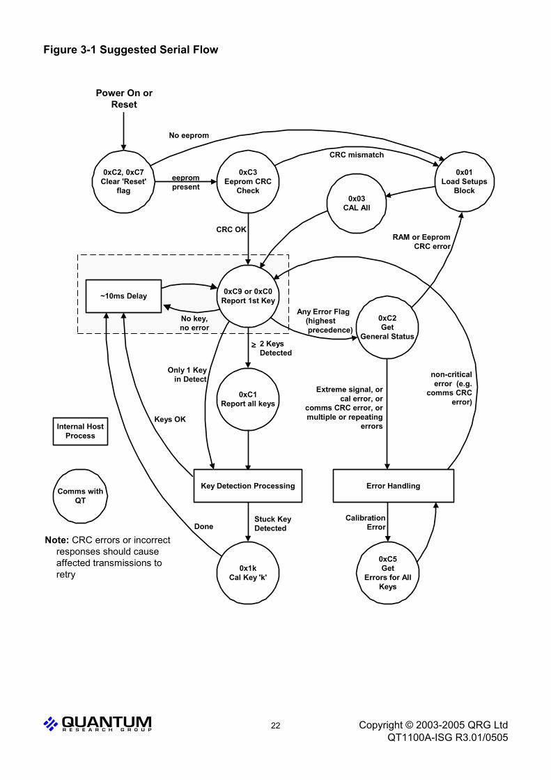
Figure 3-1 Suggested Serial Flow
L Q 22 Copyright © 2003-2005 QRG LtdQT1100A-ISG R3.01/0505
0xC3Eeprom CRC
Check
0xC1Report all keys
Only 1 Keyin Detect
0x1kCal Key 'k'
Key Detection Processing
No key,no error
mmmm 2 KeysDetected
CRC mismatch
0xC2Get
General Status
Extreme signal, orcal error, or
comms CRC error, ormultiple or repeating
errors
Power On orReset
Stuck KeyDetected
0xC5Get
Errors for AllKeys
Any Error Flag (highest precedence)
CalibrationErrorDone
Keys OK
Note: CRC errors or incorrectresponses should causeaffected transmissions toretry
Internal HostProcess
Comms withQT
0xC2, 0xC7Clear 'Reset'
flageeprompresent
No eeprom
CRC OKRAM or Eeprom
CRC error
0x01Load Setups
Block
Error Handling
non-criticalerror (e.g.
comms CRCerror)
~10ms Delay 0xC9 or 0xC0Report 1st Key
0x03CAL All
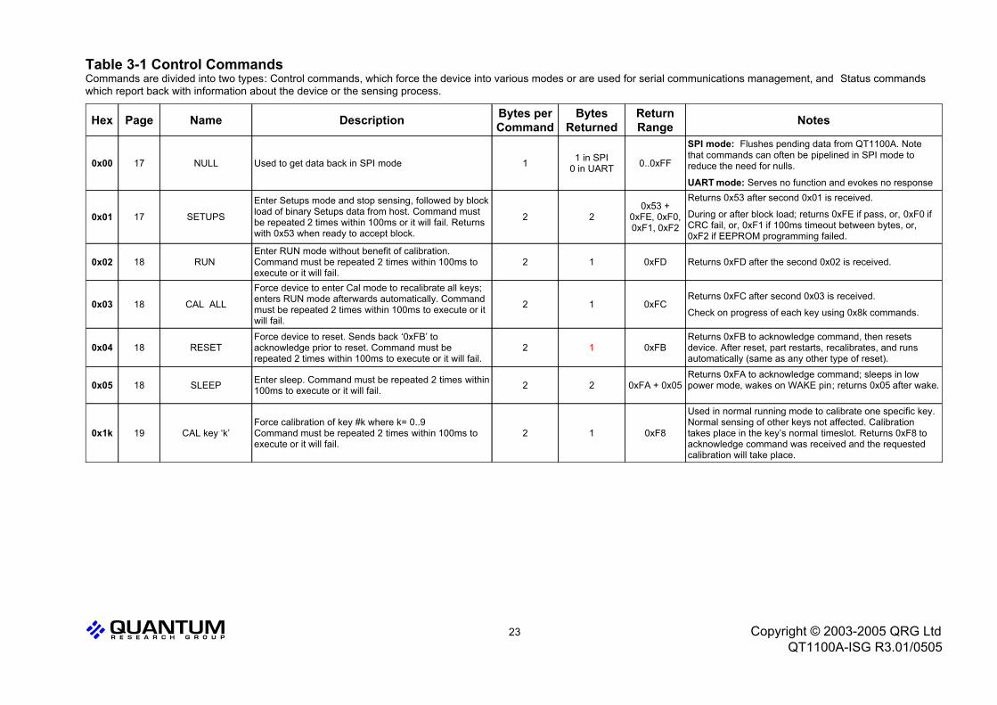
Table 3-1 Control CommandsCommands are divided into two types: Control commands, which force the device into various modes or are used for serial communications management, and Status commandswhich report back with information about the device or the sensing process.
Used in normal running mode to calibrate one specific key.Normal sensing of other keys not affected. Calibrationtakes place in the key’s normal timeslot. Returns 0xF8 toacknowledge command was received and the requestedcalibration will take place.
0xF812Force calibration of key #k where k= 0..9Command must be repeated 2 times within 100ms toexecute or it will fail.
CAL key ‘k’190x1k
Returns 0xFA to acknowledge command; sleeps in lowpower mode, wakes on WAKE pin; returns 0x05 after wake.
0xFA + 0x0522Enter sleep. Command must be repeated 2 times within100ms to execute or it will fail.SLEEP180x05
Returns 0xFB to acknowledge command, then resetsdevice. After reset, part restarts, recalibrates, and runsautomatically (same as any other type of reset).
0xFB12Force device to reset. Sends back ‘0xFB’ toacknowledge prior to reset. Command must berepeated 2 times within 100ms to execute or it will fail.
RESET180x04
Returns 0xFC after second 0x03 is received.
Check on progress of each key using 0x8k commands.0xFC12
Force device to enter Cal mode to recalibrate all keys;enters RUN mode afterwards automatically. Commandmust be repeated 2 times within 100ms to execute or itwill fail.
CAL ALL180x03
Returns 0xFD after the second 0x02 is received.0xFD12Enter RUN mode without benefit of calibration.Command must be repeated 2 times within 100ms toexecute or it will fail.
RUN 180x02
Returns 0x53 after second 0x01 is received.
During or after block load; returns 0xFE if pass, or, 0xF0 ifCRC fail, or, 0xF1 if 100ms timeout between bytes, or,0xF2 if EEPROM programming failed.
0x53 +0xFE, 0xF0,0xF1, 0xF2
22
Enter Setups mode and stop sensing, followed by blockload of binary Setups data from host. Command mustbe repeated 2 times within 100ms or it will fail. Returnswith 0x53 when ready to accept block.
SETUPS170x01
SPI mode: Flushes pending data from QT1100A. Notethat commands can often be pipelined in SPI mode toreduce the need for nulls.
UART mode: Serves no function and evokes no response
0..0xFF1 in SPI0 in UART1Used to get data back in SPI modeNULL170x00
NotesReturnRange
BytesReturned
Bytes perCommandDescriptionNamePageHex
L Q 23 Copyright © 2003-2005 QRG LtdQT1100A-ISG R3.01/0505
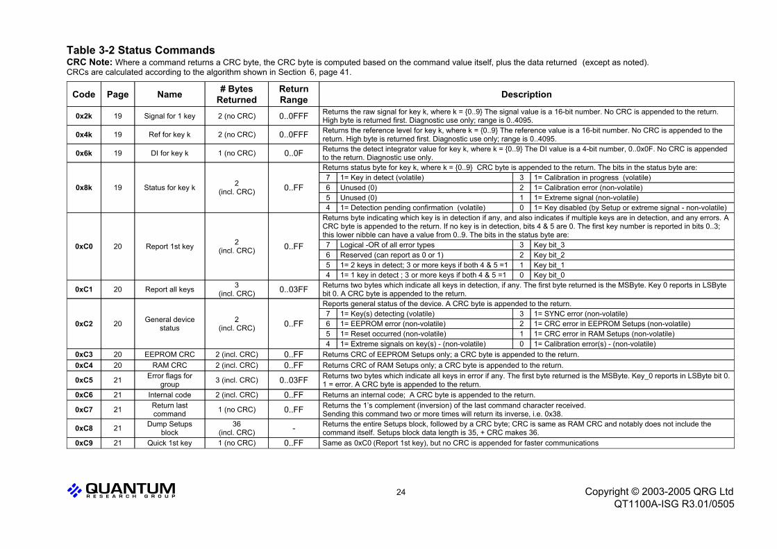
Table 3-2 Status CommandsCRC Note: Where a command returns a CRC byte, the CRC byte is computed based on the command value itself, plus the data returned (except as noted).CRCs are calculated according to the algorithm shown in Section 6, page 41.
Same as 0xC0 (Report 1st key), but no CRC is appended for faster communications0..FF1 (no CRC)Quick 1st key210xC9
Returns the entire Setups block, followed by a CRC byte; CRC is same as RAM CRC and notably does not include thecommand itself. Setups block data length is 35, + CRC makes 36.-36
(incl. CRC)Dump Setups
block210xC8
Returns the 1’s complement (inversion) of the last command character received. Sending this command two or more times will return its inverse, i.e. 0x38.0..FF1 (no CRC)Return last
command210xC7
Returns an internal code; A CRC byte is appended to the return.0..FF2 (incl. CRC)Internal code210xC6
Returns two bytes which indicate all keys in error if any. The first byte returned is the MSByte. Key_0 reports in LSByte bit 0.1 = error. A CRC byte is appended to the return. 0..03FF3 (incl. CRC)Error flags for
group210xC5
Returns CRC of RAM Setups only; a CRC byte is appended to the return.0..FF2 (incl. CRC)RAM CRC200xC4Returns CRC of EEPROM Setups only; a CRC byte is appended to the return.0..FF2 (incl. CRC)EEPROM CRC200xC3
1= Calibration error(s) - (non-volatile)01= Extreme signals on key(s) - (non-volatile)41= CRC error in RAM Setups (non-volatile)11= Reset occurred (non-volatile)51= CRC error in EEPROM Setups (non-volatile)21= EEPROM error (non-volatile)61= SYNC error (non-volatile)31= Key(s) detecting (volatile)7
Reports general status of the device. A CRC byte is appended to the return.
0..FF2(incl. CRC)
General devicestatus200xC2
Returns two bytes which indicate all keys in detection, if any. The first byte returned is the MSByte. Key 0 reports in LSBytebit 0. A CRC byte is appended to the return.0..03FF3
(incl. CRC)Report all keys200xC1
Key bit_001= 1 key in detect ; 3 or more keys if both 4 & 5 =14Key bit_111= 2 keys in detect; 3 or more keys if both 4 & 5 =15Key bit_22Reserved (can report as 0 or 1)6Key bit_33Logical -OR of all error types7
Returns byte indicating which key is in detection if any, and also indicates if multiple keys are in detection, and any errors. ACRC byte is appended to the return. If no key is in detection, bits 4 & 5 are 0. The first key number is reported in bits 0..3;this lower nibble can have a value from 0..9. The bits in the status byte are:
0..FF2(incl. CRC)Report 1st key200xC0
1= Key disabled (by Setup or extreme signal - non-volatile)01= Detection pending confirmation (volatile)41= Extreme signal (non-volatile)1Unused (0)51= Calibration error (non-volatile)2Unused (0)61= Calibration in progress (volatile)31= Key in detect (volatile)7
Returns status byte for key k, where k = {0..9} CRC byte is appended to the return. The bits in the status byte are:
0..FF2(incl. CRC)Status for key k190x8k
Returns the detect integrator value for key k, where k = {0..9} The DI value is a 4-bit number, 0..0x0F. No CRC is appendedto the return. Diagnostic use only.0..0F1 (no CRC)DI for key k190x6k
Returns the reference level for key k, where k = {0..9} The reference value is a 16-bit number. No CRC is appended to thereturn. High byte is returned first. Diagnostic use only; range is 0..4095.0..0FFF2 (no CRC)Ref for key k190x4k
Returns the raw signal for key k, where k = {0..9} The signal value is a 16-bit number. No CRC is appended to the return.High byte is returned first. Diagnostic use only; range is 0..4095.0..0FFF2 (no CRC)Signal for 1 key190x2k
DescriptionReturnRange
# BytesReturnedNamePageCode
L Q 24 Copyright © 2003-2005 QRG LtdQT1100A-ISG R3.01/0505
4 Setup Block FunctionsThe Setups block controls internal operation including criticalfunctions such as sensitivity, filtering, sample rate, andcommunications parameters. These functions aresummarized in Table 4-1, page 31.
4.1 NTHR - Negative Threshold BitsBytes 0 - 9, Bits 7..4Default value: 9Typical values: See textDisabling key(s): 0
See also Table 4-2, page 32.
The internal signal levels decrease when a key is touched.This phenomenon is related to the charge-transferacquisition conversion mechanism used by the device.
Internally the device employs a 16-bit digital reference valuefor each channel. This reference is determined during thecalibration process. After calibration, the reference is eitherlocked or can only move very slowly in response toslow-moving changes in background levels of signal.
Against this reference, the actual signal can move very fastin response to touch, but when it does so the internalnumerical signal value drops below the reference value.
The negative threshold (NTHR parameter) sets the device sensitivity by controlling the distance that the signal has totravel before creating a detection.
Each channel has its own NTHR setting; these are set in theupper nibbles of Setup bytes 0..9. NTHR can control thethreshold in one of two ways, via the NTM bit contained inbyte 32 in the Setups block:
NTM bit = 0: When NTM is clear, NTHR key settings createthresholds based on user-defined offsets from thereference levels. The offsets are based on the setting ofNTHR, plus 5 counts. Thus the available threshold rangeis from 5 to 20. If NTHR is 9, this will create a threshold14 counts below the key’s reference level. Highernumbers mean less sensitivity.
This method allows the sensitivity to be altered bychanging the value of Cs, as well as by changing thevalue of NTHR. This allows a user to conveniently alterkey sensitivity without resort to an external EEPROM orserial communications; the default key settings of N THRmean that the Cs value can be altered proportionately toincrease sensitivity. Bigger Cs = higher gain.
NTM bit = 1: When NTM is set, the NTHR settings arebased on a percentage of the signal reference level. Thismeans that if the reference level doubles, the thresholdvalue also doubles. The reference value is directlyrelated to Cs and Cx. If Cs doubles but NTHR isdetermined as a ratio, the effect is that the devicesensitivity does not change at all. Due to the physics ofthe acquisition process, increasing Cx will reducesensitivity even in this mode, just not as much as in theNTM = 0 mode.
The NTHR value in this mode is set using a percen tagecalculation as defined in Table 4-2, page 32. If the settingis set very sensitive but the burst length is short (due to asmall value of Cs and/or large value of Cx) then thecomputed threshold may be too small to process reliably.When this happens the sensitivity is limited internally to aminimum value of 3 counts of signal.
Disabling of keys: To disable a key, set NTHR for that keyto 0; this will turn the bursts off for that key but will preserveits timeslot, thus preserving all system timings which dependon the burst spacing. If the system uses the externalEEPROM or UART or SPI communication, the NTHRparameter must be used to disable a key. Using the SNSpins to disable a key will result in an error report.
In stand-alone scanport mode with no EEPROM present,keys must be disabled using default settings of SNS pins asshown on page 4.
A key that is legally disabled cannot report an error.
See Section 2.16, page 14 for more information on errorreporting.
Typical values: For most touch applications where either anEEPROM or a serial link is used, use NTM =1 and set NTHR = 10 (1.37%) to begin. Each key needs to be tailoreddue to inequalities in stray loading capacitance.
For most touch applications where ne ither an EEPROM nora serial link are used, the default setting is 9 + 5 = 14 countsof signal change. Key sensitivity can be tailored for each keyindividually by altering each Cs capacitor value.
4.2 NHYS - Negative Hysteresis BitsBytes 0 - 9, Bits 3..0Default value: 3Typical values: 3, 2
Hysteresis controls the level at which the detection processceases with respect to the threshold level NTHR. Thehysteresis is controlled by the lower 2 bits of the first 10bytes of the Setups block.
The value is expressed as a percentage of the distancemeasured from the threshold value back up towards thereference. Thus given a scenario:
Signal reference = 732NTHR = 12 countsNHYS = 25%,
then the signal has to fall to 732 - 12 = 720 to cause adetection. The signal has to then rise again to 720 + (12 * 0.25) = 723 for the detection to cease.
Each key can have its own hysteresis value.
Generally a low value of hysteresis (12.5%) is enough tosolve chatter-type problems. Excess hysteresis can causethe sensor to ‘stick on’ especially if there are underlyingproblems in wiring or the power supply.
Typical value: For most touch applications, use 12.5%.
4.3 NDCR / PDCR - Drift Comp BitsNDCR: Bytes 10 - 19, Bits 7..4PDCR: Byte 31, Bits 7..4Default NDCR value: 7Default PDCR value: 5Typical values: Tables 4-3 and4-4,
pages 32 and 33
Signals can drift because of changes in Cx and Cs over timeand temperature. It is crucial that such drift be compensated,or false detections and sensitivity shifts can occur.
Drift compensation (Figure 4-1) is performed by making thereference level track the raw signal at a slow rate, but onlywhile there is no detection in effect. The rate of adjustmentmust be performed slowly, otherwise legitimate detections
L Q 25 Copyright © 2003-2005 QRG LtdQT1100A-ISG R3.01/0505

could be ignored. The devices drift compensate using aslew-rate limited change to the reference level; the thresholdand hysteresis values are slaved to this reference.
When a finger is sensed, the signal falls due to the design ofthe signal conversion process.
Once a finger is sensed, the drift compensation mechanismceases since the signal is legitimately detecting an object.Drift compensation only works when the signal in questionhas not crossed the negative threshold level.
The drift compensation mechanism can be madeasymmetric if desired; the drift -compensation can be madeto occur in one direction faster than it does in the othersimply by changing the NDCR and PDCR Setupsparameters. NDCR can be modified on a per-key basis.
Specifically, drift compensation should be set to compensatefaster for increasing signals than for decreasing signals.Decreasing signals should not be compensated quickly,since an approaching finger could be compensated forpartially or entirely before even touching the touch pad.However, an obstruction over the sense pad, for which thesensor has already made full allowance , could suddenly beremoved leaving the sensor with an artificially suppressedreference level and thus become insensitive to touch. In thislatter case, the sensor should compensate for the object'sremoval by raising the reference level relatively quickly.
NDCR and PDCR are configured using parameters in theSetups block (page 31). The numbers entered for theseparameters are used as an entries to lookup tables found onpage 32 and page 33 respectively. The actual amount of driftcompensation can be read from these tables, which dependon the burst spacing parameter (BS).
Example: BS = 3.5ms, NDCR = 6; the NDCR rate is 2.15sper LSB change in the reference level when driftcompensating negatively (same direction as a touch).
Example: BS = 2.5ms, PDCR = 9; the PDCR rate is 1.31sper LSB change in the reference level when driftcompensating positively (opposing direction to touch).
Drift compensation and the detection time-outs worktogether to provide for robust, adaptive sensing. Thetime-outs provide abrupt changes in reference calibrationdepending on the duration of the signal 'event'.
4.4 NRD - Negative Recal Delay BitsBytes 10 - 19, Bits 3..0Default value: 5Typical values: Table 4-5, page 34
If a foreign object contacts a key the key's signal maychange enough in the negative direction, the same as anormal touch, to create an unintended detection. When thishappens it is usually desirable to cause the key tobe recalibrated to restore its function after a timedelay of some seconds.
The Negative Recal Delay timer monitors thisdetection duration; if a detection event exceeds thetimer's setting, the key will be recalibrated. After arecalibration has taken place, the affected key willonce again function normally even if it is still beingcontacted by the foreign object. This feature is seton a per-key basis. It can be disabled if desired bysetting this parameter to zero, so that it will notrecalibrate automatically (infinite timeout).
NRD is configured in the Setups block (page 31).The numbers entered for this parameter are used
as entries to a lookup table (LUT) found on page 34. Theactual delay amount can be determined from this table,which depends on the burst spacing parameter (BS).
4.5 PRD - Positive Recal Delay BitsByte 31, Bits 3..0Default value: 7Typical values: Table 4-6, page 35
A recalibration can occur automatically if the signal swingsmore positive than the positive threshold level. This conditioncan occur if there is positive drift but insufficient positive driftcompensation, or if the reference moved negative due to arecalibration, and thereafter the signal returned to normal.
As an example of the latter, if a foreign object or a fingercontacts a key for a period longer than the Negative RecalDelay (NRD), the key is by recalibrated to a new lowerreference level. Then, when the condition causing thenegative swing ceases to exist (e.g. the object is removed)the signal can suddenly swing back positive to near itsnormal reference.
It is almost always desirable in these cases to cause the keyto recalibrate quickly to the new signal level so as to restorenormal touch operation. The device accomplishes this bysimply setting Reference = Signal.
The time required to detect this condition before recalibratingis governed by PRD. For this feature to operate, the signalmust rise through the positive threshold level PTHRcontinuously for a period PRD.
After the PRD interval has expired and the recalibration hastaken place, the affected key will once again functionnormally. This interval affects all keys equally.
PRD is configured in the Setups block (page 31). Thenumbers entered for this parameter are used as entries to alookup table (LUT) found on page 35. The actual delay canbe determined from this table, which depends on the burstspacing parameter (BS).
4.6 AKS - Adjacent Key Suppression BitsBytes 20 - 29, Bit 7Default value: 0 (off)
The device incorporates adjacent key suppression (‘AKS’ -patent pending) that can be selected on a per-key basis.AKS permits the suppression of multiple key presses basedon relative signal strength. This feature assists in solving theproblem of surface moisture which can bridge a key touch toan adjacent key, causing multiple key presses. This featureis also useful for panels with tightly spaced keys, where afinger might inadvertently activate an adjacent key along withthe desired one.
L Q 26 Copyright © 2003-2005 QRG LtdQT1100A-ISG R3.01/0505
Figure 4-1 Thresholds and Drift Compensation
Threshold
Signal
Hysteresis
Reference
Output

AKS works for keys located anywhere and is not restricted tophysically adjacent keys; the device has no knowledge ofwhich keys are actually physically adjacent. When enabledfor a key, adjacent key suppression causes detections onthat key to be suppressed if any other AKS-enabled key hasa more negative signal deviation from its reference.
AKS will not function if NDIL = 1 for the key. The AKS featurerequires 2 or more scans of all keys to function, hence NDILmust be 2 or greater.
4.7 EK - Error Key Control BitsBytes 20 - 29, Bit 5Default value: 0 (off)
The EK function allows one or more keys to be forced intodetection artificially if there is a major error anywhere in thedevice including on any key. The key to be forced active isselected per-key by the EK bit; any or all 10 keys can beenabled for this function if desired. The reporting of theforced key is via any interface method - scanport, UART, orSPI, as well as the LED pin if the K2L mode for the chosenkey is enabled; note however that major errors force the LEDpin active regardless of the EK function.
The EK function allows error reporting via a redundant pathfor failure detection purposes, to make key sensing morerobust.
See also Section 3.5.7.
4.8 K2L / LEDP / KEYO Control BitsK2L: Bytes 20 - 29, Bit 4 (one per key)LEDP: Byte 32, Bit 3KEYO: Byte 34, Bit 7Default K2L value: 0 (off)Default LEDP value: 0 (active low) Default KEYO value: 0 (off)
The LED pin can be used as a health indicator, key detectindicator, and an error status. This pin can act as a backupinformation source for a host microcontroller to provide forredundant signalling. The LED pin is a full push-pull CMOSdriver.
K2L Key-To-LED Function: This bit (one per key) enablesthe associated key, when active, to force the LED pin activefor one and only one complete burst cycle (during all 10 keysstarting from timeslot 0); this is a one-shot output. If there isalso an ongoing major error, the major error takesprecedence and LED stays solid-active. The 10µs Heartbeatpulse (see below) still exists after timeslot 9. It is possible tohave multiple keys’ K2L bits enabled. K2L can be used toestablish a redundant signalling path for important ‘Halt’ or‘Panic’ keys etc. The KEYO function is overridden by K2L forone scan cycle.
K2L in Standalone Mode: K2L is automatically enabled onall keys in standalone mode when no EEPROM is present.This can be used to interrupt a host controller whenever anyenabled key is touched.
Heartbeat Pulses: At the end of each complete keyscanafter the timeslot for key 9, the LED pin will pulse low for10µs as a ‘health’ indicator. The exception to this is if theLEDP control bit is high (active high LED drive), in whichcase Heartbeat pulses are disabled. It is possible to monitorthe Heartbeat pulse in a way that confirms the device isoperating properly.
LEDP LED Polarity Function Control Bit. This bit controlsthe active polarity of the LED output. If it is 0, the LED pin is
active low (default state). If LEDP = 1, the output is activehigh. In addition, with LEDP = 1, heartbeat signals are notpresent on the LED line.
KEYO Key Output Control Bit: This bit causes the LED topulse active if there are keys in detection, during the timeslotof the active key.
In addition to the heartbeat pulse after timeslot 9, the LEDpin will pulse active during the burst of the active key’stimeslot. For example; if key 3 is active, there will be anactive KEYO pulse during the next occurrence of timeslot 3.The pulse will be as wide as the timeslot. The KEYO functionis overridden by the K2L function for one scan cycle. TheKEYO function affects all keys.
Major errors: Any major error (those not involving disabledkeys) will cause the LED pin to become solid-active. A majorerror is one where an enabled key signal falls below LBLL(Section 4.13) or rises above a value of 4095. Theseconditions can happen if the Cs capacitor fails or there is ashort in the SNS circuit. A major error also includes RAMand EEPROM CRC errors.
In Standalone Mode with no EEPROM present, keys aredisabled by strapping the SNS pins to ‘unused’ settings(Table 1.1 page 4); this will not generate a ‘major error’output unless the error occurs after the part has alreadygone through power-up calibration successfully.
The Heartbeat ‘health’ indicator does not appear when a‘major error’ condition exists. A ‘major error’ also overridesthe KEYO and K2L functions when detected.
For more information on error reporting see Section 2.16,Page 14.
4.9 NDIL, FDIL - Detect Integrator BitsNDIL: Bytes 20 - 29, Bits 3..0FDIL: Byte 32, Bits 7..4Default NDIL value: 2Default FDIL value: 5Typical values: NDIL = 2, FDIL = 5
To suppress false detections caused by spurious events likeelectrical noise, the device incorporates a 'detectionintegrator' or DI counter mechanism that acts to confirm adetection by consensus (all detections in sequence mustagree). The DI mechanism counts sequential detections of akey that appears to be touched, after each burst for the key.For a key to be declared touched, the DI mechanism mustcount to completion without even one detection failure.
The DI mechanism uses two counters. The first is the ‘fastDI’ counter FDIL. When a key’s signal is first noted to bebelow the negative threshold, the key enters ‘fast burst’mode. In this mode the burst is rapidly repeated for up to thespecified limit count of the fast DI counter. Each key has itsown counter and its own specified fast-DI limit (FDIL), whichcan range from 1 to 15. When fast-burst is entered thedevice locks onto the key and repeats the acquire burst untilthe fast-DI counter reaches FDIL, or, the detection failsbeforehand. After this the device resumes normalkeyscanning and goes on to the next key.
The ‘Normal DI’ counter counts the number of times thefast-DI counter reached its FDIL value. The Normal DIcounter can only increment once per complete scan of allkeys. Only when the Normal DI counter reaches NDIL doesthe key become tagged ‘active’.
The net effect of this is that the sensor can rapidly lock ontoand confirm a detection with many confirmations, while still
L Q 27 Copyright © 2003-2005 QRG LtdQT1100A-ISG R3.01/0505

scanning other keys. The ratio of ‘fast’ to ‘normal’ counts iscompletely user-settable via the Setups process. The totalnumber of required confirmations is equal to the product ofFDIL and NDIL.
Example: If FDIL = 5 and NDIL = 2, the total DI countrequired is 10, even though the device only scanned throughall keys twice.
The DI mechanism is extremely effective at reducing falsedetections at the expense of slower reaction times. In someapplications a slow reaction time is desirable; the DImechanism can be used to intentionally slow down touchresponse to require the user to touch longer to operate thekey.
If FDIL = 1, the device functions conventionally; eachchannel acquires only once in rotation , and the normaldetect integrator counter (NDIL) operates to confirm adetection. The Fast-DI feature is effectively disabled.
If FDIL m 2, then the fast-DI counter also operates in additionto the NDIL counter.
If the key has not yet been declared active, the followingtakes place:
1. If (Signal [NTHR): The signal is strong, and the fast-DIcounter is incremented towards FDIL. Once FDIL isreached, the Normal DI counter increments once.
2. If (Signal > NTHR): Both the fast-DI and normal DIcounters are cleared due to lack of sufficient signal.
3. If (Normal DI counter = NDIL): The key is declaredactive.
Once the key is declared active, the following takes place:
1. If (Signal [ NTHR): The signal is still strong enough tosustain key detection. The key remains in detection,and the Normal DI counter increments if it is less thanNDIL.
2. If (Signal > NTHR) and (Signal [ NHYS): The keysignal is weak, however the key remains in detectionand the Normal DI counter remains unchanged.
3. If (Signal > NHYS): There is insufficient signal tosustain key detection, and the Normal DI counter isdecremented towards 0.
4. If (Normal DI counter = 0), the key is declared inactive.
4.10 PTHR - Positive Threshold BitsByte 30, Bits 7..4Default value: 5Typical value: 4 - 10
The positive threshold is used to provide a mechanism forrecalibration of the reference point when a key signal movesabruptly to the positive. This condition is abnormal; it usuallyoccurs after a prolonged touch has caused an automaticrecalibration via the NRD parameter, and a subsequentremoval of touch causes the signal to rise abruptly above thereference level.
The normal desire is to recover from these events quickly ,usually in a second or two. PTHR is the upper threshold forthe detection of these anomalies; PHYS is the correspondinghysteresis value (see below) used to provide a stabledetection criteria. Positive recal delay (PRD) is the timingfunction used to time when the key is recalibrated once thepositive excursion has been noted.
For a further description see PHYS below.
Positive drift compensation (PDCR) also works to restoresignal levels that are erroneously positive. However thismechanism is much slower and is used primarily tocompensate for longer term drift factors, whereas PTHR isused to compensate more quickly for fast rises in signalvalue.
The PTHR parameter is global to all keys; it is a single byteparameter common to all . It is measured in counts of signaland can be set from 2..15.
4.11 PHYS - Positive Hysteresis BitsByte 30, Bit 3..0Default value: 1Typical value: 10% of PTHR or 1 count
(whichever is greater)
Positive hysteresis is used in setting the drop out level atwhich a positive detection ceases (see PTHR above).
The value is expressed as a signal count from the positivethreshold value back down towards the reference. Thusgiven a scenario:
Reference = 732PTHR = 5 countsPHYS = 1,
then the signal has to rise to 732 + 5 = 737 to cause apositive detection. At this point the positive recal delay (PRD)engages and starts timing the signal excursion. Providingthat the signal level does not fall below 736 (1 count ofhysteresis below 737) the timer will continue until it expires,at which point the affected key is fully recalibrated (and onlythat key).
The PHYS parameter is global to all keys; it is a single byteparameter common to all . It is measured in counts of signaland can be set from 0..15.
4.12 SE, SYNC Control BitsByte 32, Bits 1, 0Default SE value: 0 (off)Default SYNC value: 0 (level sensing)
The Sync functions allow the device to synchronize toexternal clock sources or to other similar devices to preventinterference effects.
Most interference in capacitance sensors comes from beatfrequency and alias generation due to non-coherencybetween the sampling rate of the sensor and an externalnoise source. Another similar sensor can be considered anoise source.
The QT1100A offers two ways to limit this kind ofinterference:
1. Level sensing: Make sure the QT1100A does notsample at the same time as a similar device, wherephysically adjacent keys are concerned.
2. Edge sensing: Synchronize the QT1100A to an externalrepetitive noise source so that there are no beatfrequencies generated and the interference shows up asa benign DC offset to the acquired signal.
The SE (‘Sync Enable’) bit determines whether or not Syncis used. SYNC can be enabled by setting SE = 1. If SE = 0,the part runs asynchronously regardless of the state of theSYNC pin. The SYNC bit determines which mode, 1 or 2, thedevice operates in if SE = 1.
L Q 28 Copyright © 2003-2005 QRG LtdQT1100A-ISG R3.01/0505

SE in Standalone Mode: SE is automatically enabled (= 1)in standalone mode when no EEPROM is present.
SYNC Mode: If SYNC = 0, the device uses the Sync pin tocommunicate to another similar part (e.g. one or moreadditional QT1100A’s). QT1100A’s connected together inthis way will self- synchronize so that they all acquire on Key0 at the same time. Provided that the devices run at a similarclock rate and have the same burst spacing (BS) parametersthe devices will remain locked over their full acquisitioncycles, key for key. In this condition it is easy to design aPCB where keys from multiple QT1100A’s are physicallyadjacent but not of the same key number; thus ensuring thatadjacent keys are never acquiring at the same time andcannot interfere with each other.
Level Mode: If SYNC = 0, the device operates in a levelsensing mode. The open-drain SYNC pin is pulled low byeach device that is currently sensing on any key but key 0.After the last key is sensed (key 9) the device floats theSYNC pin and then waits until the SYNC pin actually floatshigh. Any other devices sharing the SYNC pin will also clampthe SYNC pin low until they are done sensing all their keys.Finally when all devices are waiting to start acquiring on key0, the SYNC line will actually float high, and the sensordevices will then all acquire key 0 in unison.
Edge Mode: If SYNC = 1, the part waits for a positive edgeon the SYNC pin to begin acquiring on key 0. Thereafter theother keys also acquire in sequence according to the BSsetup.
SYNC = 1 should be used for external noise source or powerline synchronization. A simple RC circuit can be connectedfrom a mains supply to the SYNC pin to ensure phase-aligned triggering. SYNC can operate from 10Hz ~ 400Hz.
If SE = 1 in UART mode, holding pin RX = 0 for excessiveperiods, or in SPI mode, holding pin /SS = 0, will preventproper operation of SYNC. Since communication has higherpriority than SYNC, communicating during a SYNC activeedge will cause an additional delay of the SYNC process andresult in timing skews. Holding either /SS or RX lowcontinuously will inhibit SYNC.
These control bits apply to the device as a whole.
4.13 LBLL - Lower Burst Length LimitByte 33Default value: 3Typical value: 50 - 100
LBLL is an FMEA-oriented limits feature used to detect keysthat are not operating properly. If a key is short circuited, orits Cs/Rs sensing circuit has failed, the acquired signal willbe either one count or attempt to be infinite.
Lower errors are caught using the LBLL parameter whichcan be set from 0 to 255. If {signal < LBLL}, the key isflagged as having an error and the acquisition burst for thatkey is also disabled until the part is reset or the key isrecalibrated. Setting LBLL = 0 will disable this error detectionfeature and also stop the ability of a key to be self-disabled ifthere is a serious hardware error.
A better method for disabling the LBLL feature is to set it to avery low value such as 3. This way the device can still stopacquiring on channels that have serious hardware problems,yet not generate errors when signals are merely very low.
If LBLL is set too high, it could cause legitimate touchdetections to trigger an error flag and self-disable a channel.
Upper errors are caught using a built-in, fixed upper burstlength limit of 4095; beyond this value of signal, the key istagged as being in error.
4.14 BS - Burst Spacing Control BitsByte 34, Bits 4,3,2Default value: 2 (3ms)Typical values: 1 - 4
The interval of time from the start of a burst on one key tothe start of the burst on the next key is known as the burstspacing. This is an alterable parameter which affects allkeys. The burst spacing can be viewed as a timeslot in whichan acquisition burst occurs. This approach results in anorderly and predictable sequencing of key scanning withpredictable response times.
Shorter spacings result in a faster response time to touch;longer spacings permit higher burst lengths and longerconversion times but slow down response time.
Standard BS settings from 2ms to 7ms are available. BSshould be set so that the acquire burst lengths themselvesare fully contained in their timeslots, plus 500µs left over.This can be determined by using a 10x scope probe with a470K resistor in series and examining the length of thedistorted waveform (this is done to minimize loading effectswhich reduce the burst length).
If an acquisition burst exceeds its timeslot, the device will stilloperate properly except that time based parameters will beincreased in duration; the timeslots will expand to fill theburst length which is always variable.
The BS value is obtained via a lookup table (LUT) :
4.15 BR - Baud Rate Control BitsByte 34, Bits 1, 0Default value: 1 (9600)
The BR setting allows control over the baud rate, from 4800to 28.8K Baud according to the following table:
If the Baud rate is altered via serial communications, the newBaud rate is effective immediately after the Setup blockloads are complete, that is, after the QT1100A sends thefinal response from the Load Setup command (0x01).
L Q 29 Copyright © 2003-2005 QRG LtdQT1100A-ISG R3.01/0505
7.0ms76.0ms65.0ms54.0ms43.5ms33.0ms22.5ms12.0ms0
SettingBS Value
28,800319,20029,60014,8000
SettingBR Value

4.16 HCRC - Host CRCByte 35HCRC is an 8-bit CRC code calculated according to CCITT-8(see page 41) appended to the end of the Setups table. Thiscode must be sent with each serial transmission of theSetups block.
An error in the CRC will manifest itself as an error code , andif this occurs, factory default parameters will be automaticallyloaded to provide a ‘safe’, defined recovery .
The CRC can also be replaced with a 0xD6 which will inhibitCRC checking. Care should be taken so that the CRC isnever actually 0xD6 (if CRC checking is desired). This canbe done by altering any unused Setup parameter.
L Q 30 Copyright © 2003-2005 QRG LtdQT1100A-ISG R3.01/0505

Table 4-1 Serial / EEPROM Setups BlockData can be sent from the host to the QT1100A in a block of hex data over a serial port. A Setups block received via serial transmission is loaded into RAM (and also into EEPROMif one is connected). Setups mode is initiated by sending two sequential 0x01 commands to the device. If each byte in the block load sequence is not within 100ms of the precedingbyte, the command will fail and default values or EEPROM values will be used instead of the received Setups block.
EEPROM Setups are a copy of RAM Setups except that EEPROM location 0 will contain 0xD6. Location 0 of the EEPROM must contain 0xD6 or it will not be read. The Setupsblock can also be preloaded into EEPROM to control stand-alone (scanport) mode. If the initial 0xD6 is read at power-up, the remainder of the EEPROM is then loaded (providedthe EEPROM CRC is acceptable). EEPROM address location 1 corresponds to Setups block byte 0. If the last EEPROM byte is also fixed at 0xD6 in place of a CRC, EEPROMCRC checking is disabled.
Note: After any Setups changes, the part should be recalibrated using 0x03 (Enter Cal mode).
Data area is 35 bytes; plus CRC makes 36. EEPROM area has 37 bytes which also includes an initial 0xD6 byte.36-Block length
30CRC of above Setups block (0xD6 disables CRC checking). See page 41 for algorithm.<computed value>Device81HCRCHost CRC0x2335
27-
29-
29
Bit_7 = LED pin also shows keypress if KEYO = 1 Bit_6,5 = UnusedBit_4,3,2 = Burst spacing (BS), 8 values in increasing order -
2ms, 2.5ms, 3ms, 3.5ms, 4ms, 5ms, 6ms, 7ms settingsBit_1,0 = Baud rate (BR); 4 values; UART mode only
4800, 9600 (default), 19.2K, 28.8K in increasing order
0 (disable)3 (binary ‘11’)
2 (3ms)
1 (9600)
Device-
Device
Device
123
2
0, 1-
0..7
0..3
1
KEYOUnused
BS
BRControl bits0x2234
29Lower limit of acceptable burst length; below this, declares error.Default = 3 (error on catastrophic channel failure)0x031080..2551LBLLLower BL Limit0x2133
27272528-
28
Upper nibble = Fast Neg DI limit; min = 1 Bit_3: 1 = LED pin is inverted Bit_2: 1 = Ratiometric neg thesh; 0 = fixed thresholds. Bit_1: 1 = Sync enabled (default = 0, disabled)
Note: In Standalone Mode with no EEPROM, SYNC = 1 (enabled)Bit_0: SYNC mode (default = 0, level; 1 = edge)
50 (normal)0 (fixed)0 (off)*
0 (level)
10Device
10Device
Device
4111
1
1..150, 10, 10, 1
0, 1
1
FDILLEDPNTMSE
SYNC
Fast (neg) DI LimitLED PolarityNeg Thresh ModeSync Enable
Sync pin mode
0x2032
2526
Upper nibble = PDCR; 0 = no PDC; (via LUT, page 33)Lower nibble = PRD; (via LUT, page 35)
5 (0.68s @3ms)7 (1.03s @3ms)
1010
44
0..150..151PDCR
PRDPos drift comp ratePos recal delay0x1F31
2828
Upper nibble = Pos threshold; sets sensitivity to +recal Lower nibble = Pos hysteresis, counts down from +thresh
51
1010
44
2..150..151PTHR
PHYSPos threshPos hyst0x1E30
26-
2727-
27
Bit_7: 1 = AKS enable (each key)Bit_6: UnusedBit_5: EK - Key forced active on major error (each key)Bit_4: 1 = Key to LED function enable (each key)
Note: In Standalone Mode with no EEPROM, K2L = 1 (enabled) on all keysLower nibble = Norm DI Limit; Thresh crossings to detection; min = 1
0 (disable)0
0 (off)0 (off)*
2
1-11
1
1111
4
0, 1-
0, 10, 1
1..15
10
AKSUnused
EKK2L
NDIL
AKS enableUnusedError KeyKey To LED
Normal det int limit
0x14..0x1D20..29
2526
Upper nibble = NDCR; 0 = no NDC (via LUT, page 32)Lower nibble = NRD; 0 = infinite (via LUT, page 34)
7 (2.18s @3ms)5 (14.42s @3ms)
11
44
0..150..1510NDCR
NRDNeg drift comp rateNeg recal delay0x0A..0x1310..19
25-
25
Upper nibble = Neg threshold; 0 = key disabledBit_3, 2: Unused Lower nibble = Neg hysteresis, 3 = 12.5%, 2 = 25%, 1 = 50%, 0 = 0%
903
1-1
422
0..15-
0..310
NTHRUnusedNHYS
Neg threshUnusedNeg hyst
0x00..0x090..9
PageDescriptionDefaultValue
KeyScopeBits
ValidRange
ByteLenSymParameterBlock Byte #
L Q 31 Copyright © 2003-2005 QRG LtdQT1100A-ISG R3.01/0505
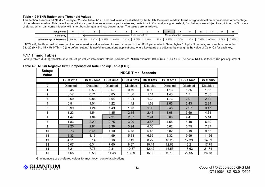
Table 4-2 NTHR Ratiometric Threshold ValuesThis section assumes bit NTM = 1 (in byte 32 - see Table 4-1). Threshold values established by the NTHR Setup are made in terms of signal deviation expressed as a percentageof the reference value. This gives key sensitivity a great tolerance towards part variances, deviations in Cs , and to a good extent, Cx. Settings are subject to a minimum of 3 countsof signal, which can come into play with short burst lengths and low percentages. The values are as follows:
0.39%0.59%0.78%0.98%1.17%1.37%1.56%1.95%2.34%2.73%3.13%3.91%4.69%5.47%6.25%disabled✁✁✁✁ Percentage of Reference
Less sensitive More sensitive-Sensitivity
1514131211109876543210Setup Value
If NTM = 0, the threshold is based on the raw numerical value entered for each channel in the NTHR parameter in Setup bytes 0..9 plus 5 co unts, and can thus range from 5 to 20 (0 + 5... 15 + 5). NTM = 0 (the default setting) is useful in standalone applications, where key gains are adjusted by changing the value of Cs or Cx for each key.
4.17 Timing TablesLookup tables (LUTs) translate several Setups values into actual internal parameters. NDCR example: BS = 4ms, NDCR = 6. The actual NDCR is then 2.46s per adjustment.
Table 4-3 NDCR Negative Drift Compensation Rate Lookup Table (LUT)
-12726.7822.9519.1315.3013.3911.489.567.6515-10321.7418.6315.5312.4210.879.317.766.2114-8417.7515.2112.6810.148.877.606.345.0713-6814.3912.3310.288.227.196.165.144.1112-5511.669.998.326.665.834.994.163.3311-459.558.196.825.464.784.103.412.7310-377.876.755.624.503.943.382.812.259-306.405.494.583.663.202.752.291.838-245.144.413.682.942.572.211.841.477-204.313.693.082.462.151.851.541.236-163.472.972.481.981.731.491.240.995-132.842.432.031.621.421.221.010.814-112.422.071.731.381.211.040.860.693-92.001.711.431.141.000.850.710.572-71.581.351.130.900.790.670.560.4510DisabledDisabledDisabledDisabledDisabledDisabledDisabledDisabled0
BS = 7ms BS = 6ms BS = 5ms BS = 4ms BS = 3.5ms BS = 3ms BS = 2.5ms BS = 2ms 1.23
LUTValueNDCR Time, SecondsSetups
Value
Gray numbers are preferred values for most touch control applications
L Q 32 Copyright © 2003-2005 QRG LtdQT1100A-ISG R3.01/0505
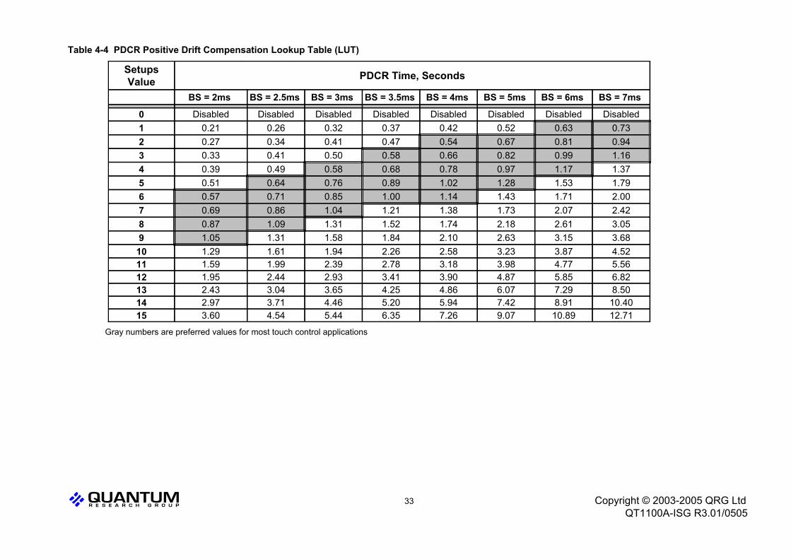
Table 4-4 PDCR Positive Drift Compensation Lookup Table (LUT)
6012.7110.899.077.266.355.444.543.60154910.408.917.425.945.204.463.712.9714408.507.296.074.864.253.653.042.4313326.825.854.873.903.412.932.441.9512265.564.773.983.182.782.391.991.5911214.523.873.232.582.261.941.611.2910173.683.152.632.101.841.581.311.059143.052.612.181.741.521.311.090.878112.422.071.731.381.211.040.860.69792.001.711.431.141.000.850.710.57681.791.531.281.020.890.760.640.51561.371.170.970.780.680.580.490.39451.160.990.820.660.580.500.410.33340.940.810.670.540.470.410.340.27230.730.630.520.420.370.320.260.2110DisabledDisabledDisabledDisabledDisabledDisabledDisabledDisabled0
BS = 7ms BS = 6ms BS = 5ms BS = 4ms BS = 3.5ms BS = 3ms BS = 2.5ms BS = 2ms 1.23
LUTValuePDCR Time, SecondsSetups
Value
Gray numbers are preferred values for most touch control applications
L Q 33 Copyright © 2003-2005 QRG LtdQT1100A-ISG R3.01/0505

Table 4-5 NRD Negative Recal Delay Lookup Table (LUT)
-127267.8229.5191.3153.0133.9114.895.676.515-103217.3186.3155.3124.2108.793.277.662.114-84177.4152.1126.8101.488.776.063.450.713-68143.8123.3102.882.271.961.651.441.112-55116.699.983.366.658.350.041.633.311-4595.581.968.354.647.841.034.127.310-3778.867.556.345.039.433.828.122.59-3064.054.945.836.632.027.422.918.38-2451.544.136.829.425.722.118.414.77-2043.036.930.824.621.518.415.412.36-1634.629.724.819.817.314.912.49.95-1328.424.320.316.214.212.210.18.14-1124.120.717.313.812.110.48.66.93-919.917.114.311.410.08.67.15.72-715.813.511.39.07.96.85.64.510InfiniteInfiniteInfiniteInfiniteInfiniteInfiniteInfiniteInfinite0
BS = 7ms BS = 6ms BS = 5ms BS = 4ms BS = 3.5ms BS = 3ms BS = 2.5ms BS = 2ms 1.23
LUTValueNRD Time, SecondsSetups
Value
Gray numbers are preferred values for most touch control applications
L Q 34 Copyright © 2003-2005 QRG LtdQT1100A-ISG R3.01/0505
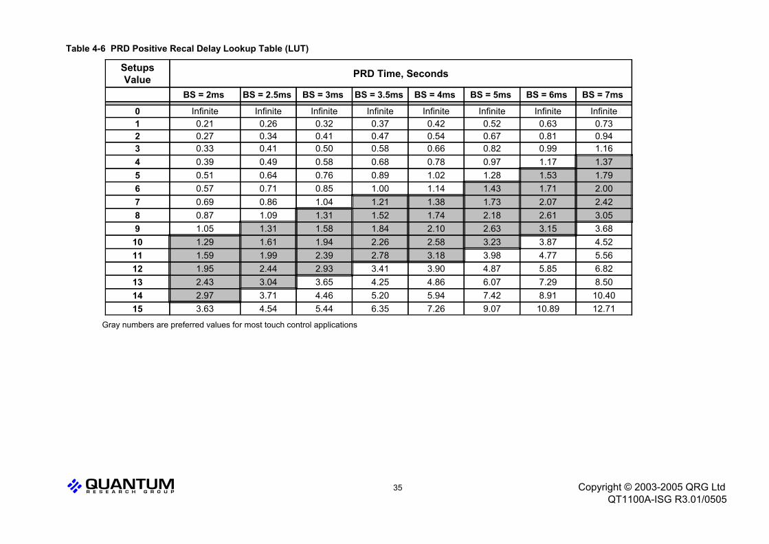
Table 4-6 PRD Positive Recal Delay Lookup Table (LUT)
6012.7110.899.077.266.355.444.543.63154910.408.917.425.945.204.463.712.9714408.507.296.074.864.253.653.042.4313326.825.854.873.903.412.932.441.9512265.564.773.983.182.782.391.991.5911214.523.873.232.582.261.941.611.2910173.683.152.632.101.841.581.311.059143.052.612.181.741.521.311.090.878112.422.071.731.381.211.040.860.69792.001.711.431.141.000.850.710.57681.791.531.281.020.890.760.640.51561.371.170.970.780.680.580.490.39451.160.990.820.660.580.500.410.33340.940.810.670.540.470.410.340.27230.730.630.520.420.370.320.260.2110InfiniteInfiniteInfiniteInfiniteInfiniteInfiniteInfiniteInfinite0
BS = 7ms BS = 6ms BS = 5ms BS = 4ms BS = 3.5ms BS = 3ms BS = 2.5ms BS = 2ms 1.23
LUTValuePRD Time, SecondsSetups
Value
Gray numbers are preferred values for most touch control applications
L Q 35 Copyright © 2003-2005 QRG LtdQT1100A-ISG R3.01/0505
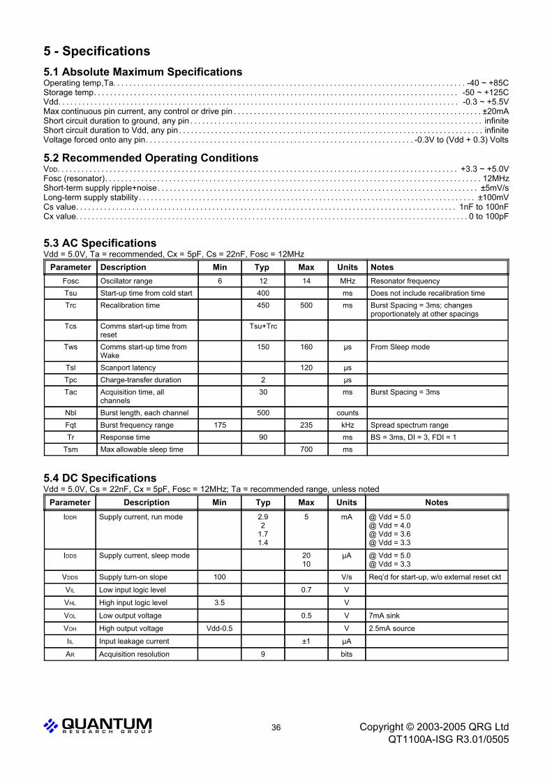
5 - Specifications5.1 Absolute Maximum SpecificationsOperating temp,Ta. . . . . . . . . . . . . . . . . . . . . . . . . . . . . . . . . . . . . . . . . . . . . . . . . . . . . . . . . . . . . . . . . . . . . . . . . . . . . . . . . . . . . . . . -40 ~ +85CStorage temp. . . . . . . . . . . . . . . . . . . . . . . . . . . . . . . . . . . . . . . . . . . . . . . . . . . . . . . . . . . . . . . . . . . . . . . . . . . . . . . . . . . . . . . . . . . -50 ~ +125CVdd. . . . . . . . . . . . . . . . . . . . . . . . . . . . . . . . . . . . . . . . . . . . . . . . . . . . . . . . . . . . . . . . . . . . . . . . . . . . . . . . . . . . . . . . . . . . . . . . . . . . -0.3 ~ +5.5VMax continuous pin current, any control or drive pin . . . . . . . . . . . . . . . . . . . . . . . . . . . . . . . . . . . . . . . . . . . . . . . . . . . . . . . . . . . . . . ±20mAShort circuit duration to ground, any pin . . . . . . . . . . . . . . . . . . . . . . . . . . . . . . . . . . . . . . . . . . . . . . . . . . . . . . . . . . . . . . . . . . . . . . . . . infiniteShort circuit duration to Vdd, any pin . . . . . . . . . . . . . . . . . . . . . . . . . . . . . . . . . . . . . . . . . . . . . . . . . . . . . . . . . . . . . . . . . . . . . . . . . . . . infiniteVoltage forced onto any pin. . . . . . . . . . . . . . . . . . . . . . . . . . . . . . . . . . . . . . . . . . . . . . . . . . . . . . . . . . . . . . . . . . . -0.3V to (Vdd + 0.3) Volts
5.2 Recommended Operating ConditionsVDD. . . . . . . . . . . . . . . . . . . . . . . . . . . . . . . . . . . . . . . . . . . . . . . . . . . . . . . . . . . . . . . . . . . . . . . . . . . . . . . . . . . . . . . . . . . . . . . . . . . . +3.3 ~ +5.0VFosc (resonator). . . . . . . . . . . . . . . . . . . . . . . . . . . . . . . . . . . . . . . . . . . . . . . . . . . . . . . . . . . . . . . . . . . . . . . . . . . . . . . . . . . . . . . . . . . . . . 12MHzShort-term supply ripple+noise. . . . . . . . . . . . . . . . . . . . . . . . . . . . . . . . . . . . . . . . . . . . . . . . . . . . . . . . . . . . . . . . . . . . . . . . . . . . . . . . ±5mV/sLong-term supply stability. . . . . . . . . . . . . . . . . . . . . . . . . . . . . . . . . . . . . . . . . . . . . . . . . . . . . . . . . . . . . . . . . . . . . . . . . . . . . . . . . . . . ±100mVCs value. . . . . . . . . . . . . . . . . . . . . . . . . . . . . . . . . . . . . . . . . . . . . . . . . . . . . . . . . . . . . . . . . . . . . . . . . . . . . . . . . . . . . . . . . . . . . . . 1nF to 100nFCx value. . . . . . . . . . . . . . . . . . . . . . . . . . . . . . . . . . . . . . . . . . . . . . . . . . . . . . . . . . . . . . . . . . . . . . . . . . . . . . . . . . . . . . . . . . . . . . . . . . 0 to 100pF
5.3 AC SpecificationsVdd = 5.0V, Ta = recommended, Cx = 5pF, Cs = 22nF, Fosc = 12MHz
ms700Max allowable sleep timeTsmBS = 3ms, DI = 3, FDI = 1ms90Response timeTrSpread spectrum rangekHz235175Burst frequency rangeFqt
counts500Burst length, each channelNbl
Burst Spacing = 3msms30Acquisition time, allchannels
Tacµs2Charge-transfer durationTpcµs120Scanport latencyTsl
From Sleep modeµs160150Comms start-up time fromWake
Tws
Tsu+TrcComms start-up time fromreset
Tcs
Burst Spacing = 3ms; changesproportionately at other spacings
ms500450Recalibration timeTrcDoes not include recalibration timems400Start-up time from cold startTsuResonator frequencyMHz14126Oscillator rangeFosc
NotesUnitsMaxTypMinDescriptionParameter
5.4 DC SpecificationsVdd = 5.0V, Cs = 22nF, Cx = 5pF, Fosc = 12MHz; Ta = recommended range, unless noted
bits9Acquisition resolutionAR
µA±1Input leakage currentIIL
2.5mA sourceVVdd-0.5High output voltageVOH
7mA sinkV0.5Low output voltageVOL
V3.5High input logic levelVHL
V0.7Low input logic levelVIL
Req’d for start-up, w/o external reset cktV/s100Supply turn-on slopeVDDS
@ Vdd = 5.0@ Vdd = 3.3
µA2010
Supply current, sleep modeIDDS
@ Vdd = 5.0@ Vdd = 4.0@ Vdd = 3.6@ Vdd = 3.3
mA52.92
1.71.4
Supply current, run modeIDDR
NotesUnitsMaxTypMinDescriptionParameter
L Q 36 Copyright © 2003-2005 QRG LtdQT1100A-ISG R3.01/0505

5.5 Burst / Sync TimingSee Section 5.7 for timing parameters
L Q 37 Copyright © 2003-2005 QRG LtdQT1100A-ISG R3.01/0505
Twbl
floats highMode 0 (level sensing) Sync shown
SYNC
Key 0 BurstBurst_Key0
Key 1 BurstBurst_Key1
T3
CRDY
Twbs
Twcrdy
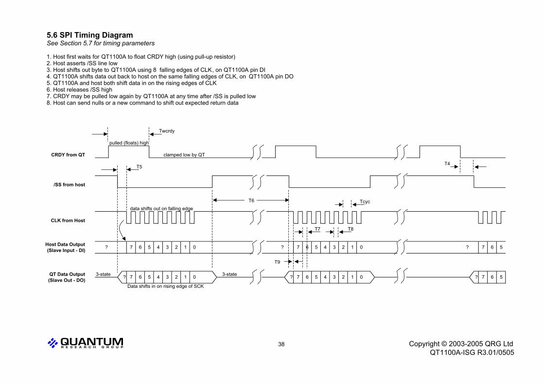
5.6 SPI Timing Diagram See Section 5.7 for timing parameters
1. Host first waits for QT1100A to float CRDY high (using pull-up resistor)2. Host asserts /SS line low3. Host shifts out byte to QT1100A using 8 falling edges of CLK, on QT1100A pin DI4. QT1100A shifts data out back to host on the same falling edges of CLK, on QT1100A pin DO5. QT1100A and host both shift data in on the rising edges of CLK6. Host releases /SS high7. CRDY may be pulled low again by QT1100A at any time after /SS is pulled low8. Host can send nulls or a new command to shift out expected return data
L Q 38 Copyright © 2003-2005 QRG LtdQT1100A-ISG R3.01/0505
Twcrdy
pulled (floats) high
CRDY from QT clamped low by QT
T5
/SS from host
data shifts out on falling edge
CLK from Host
Host Data Output(Slave Input - DI)
QT Data Output 3-state 3-state(Slave Out - DO)
Data shifts in on rising edge of SCK
0
? 7
? 7
1 0
7 6 5 4 3 2 1 0
4 3 2 1? 7 6 5 5 4 3 20 7 6? 6 5
? 6 54 3 2 1? 7 6 5
T7
Tcyc
T8
T6
T9
T4
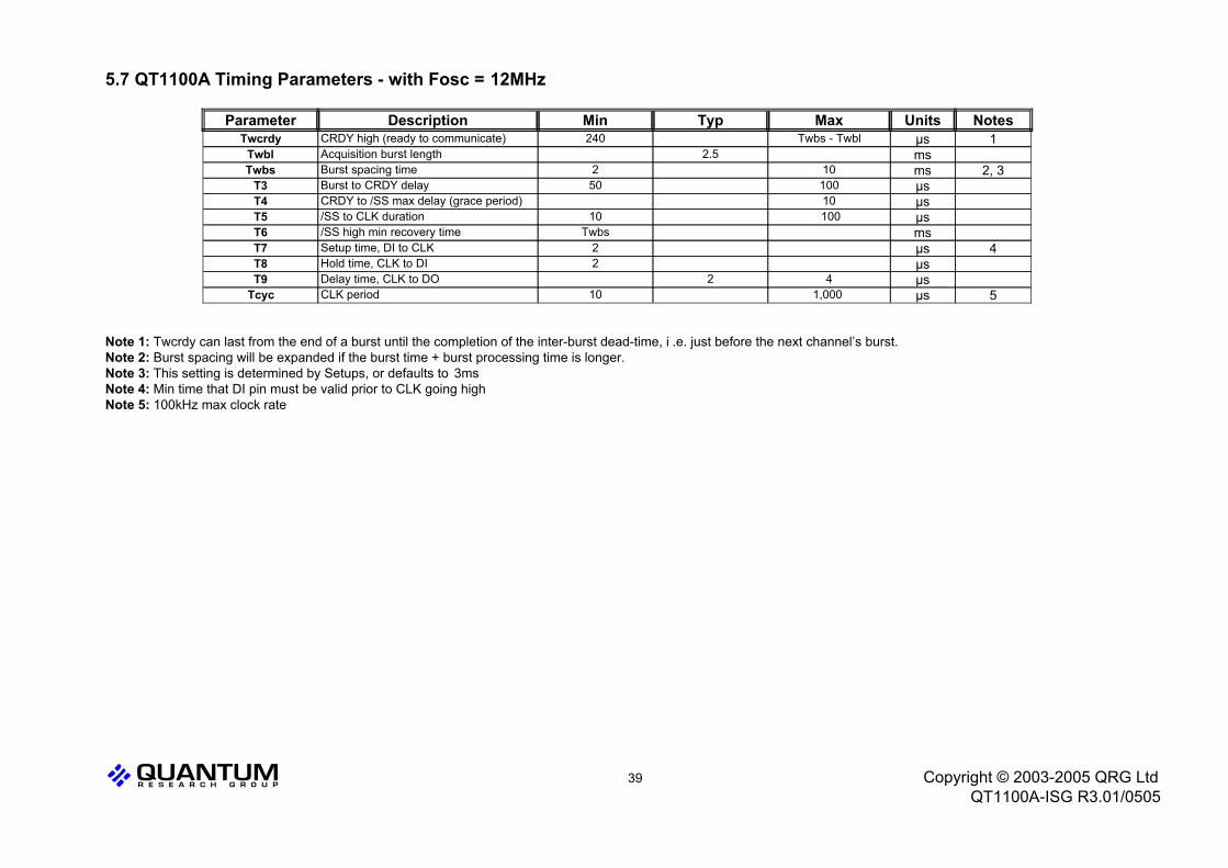
5.7 QT1100A Timing Parameters - with Fosc = 12MHz
Note 1: Twcrdy can last from the end of a burst until the completion of the inter-burst dead-time, i .e. just before the next channel’s burst.Note 2: Burst spacing will be expanded if the burst time + burst processing time is longer.Note 3: This setting is determined by Setups, or defaults to 3msNote 4: Min time that DI pin must be valid prior to CLK going highNote 5: 100kHz max clock rate
L Q 39 Copyright © 2003-2005 QRG LtdQT1100A-ISG R3.01/0505
5µs1,000 10CLK periodTcycµs42 Delay time, CLK to DOT9µs 2Hold time, CLK to DIT8
4µs 2Setup time, DI to CLKT7ms Twbs/SS high min recovery timeT6µs 100 10/SS to CLK durationT5µs10 CRDY to /SS max delay (grace period)T4µs100 50Burst to CRDY delayT3
2, 3ms10 2Burst spacing timeTwbsms 2.5 Acquisition burst lengthTwbl
1µsTwbs - Twbl 240CRDY high (ready to communicate)TwcrdyNotesUnitsMaxTypMinDescriptionParameter
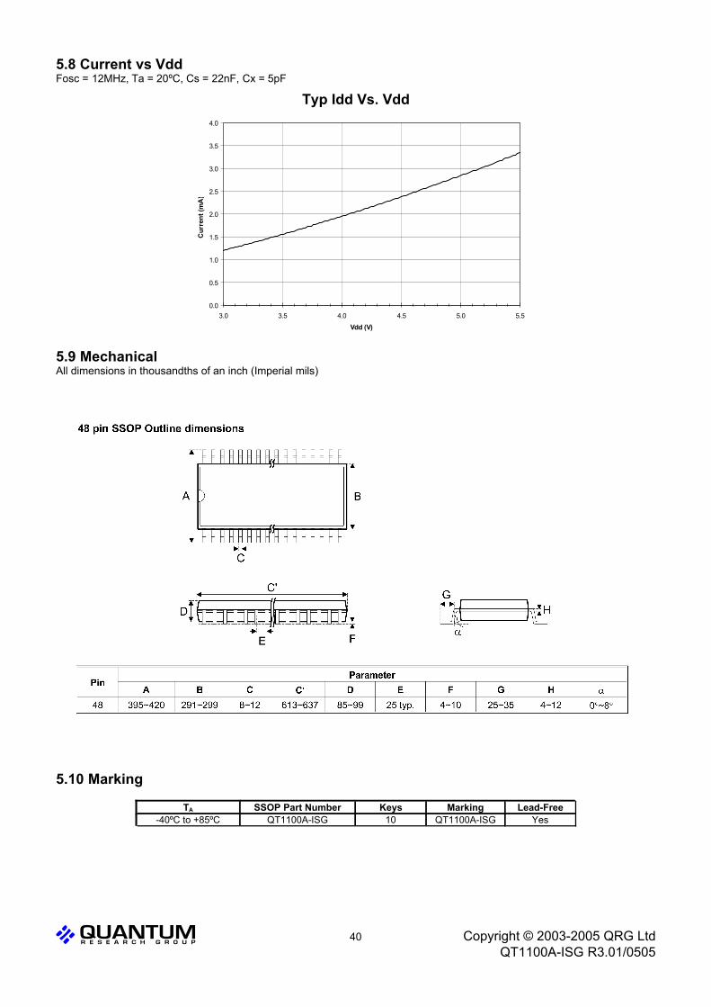
5.8 Current vs VddFosc = 12MHz, Ta = 20ºC, Cs = 22nF, Cx = 5pF
Typ Idd Vs. Vdd
5.9 MechanicalAll dimensions in thousandths of an inch (Imperial mils)
5.10 Marking
L Q 40 Copyright © 2003-2005 QRG LtdQT1100A-ISG R3.01/0505
0.0
0.5
1.0
1.5
2.0
2.5
3.0
3.5
4.0
3.0 3.5 4.0 4.5 5.0 5.5
Vdd (V)
Cur
rent
(mA
)
YesQT1100A-ISG10QT1100A-ISG-40ºC to +85ºCLead-FreeMarkingKeysSSOP Part NumberTA

6 Appendix A - 8-Bit CRC C Algorithm
// 8-bit crc calculation. Initial value is 0.// polynomial = X8 + X5 + X4 + 1// data is an 8 bit number; crc is an 8-bit number
int eight_bit_crc(int crc, int data){ int index; // shift counter
int fb;
index = 8; // initialise the shift counterdo{ fb = (crc ^ data) & 0x01;
data >>= 1;crc >>= 1;
if(fb){ crc ^= 0x8c; }
} while(--index);
return crc;}
A CRC calculator for Windows is available free of charge from Quantum Research.
L Q 41 Copyright © 2003-2005 QRG LtdQT1100A-ISG R3.01/0505

lQ Copyright © 2001-2005 QRG Ltd. All rights reservedPatented and patents pending worldwide
Corporate Headquarters1 Mitchell Point
Ensign Way, Hamble SO31 4RFGreat Britain
Tel: +44 (0)23 8056 5600 Fax: +44 (0)23 80565600
www.qprox.com
North America651 Holiday Drive Bldg. 5 / 300
Pittsburgh, PA 15220 USATel: 412-391-7367 Fax: 412-291-1015
This device covered under one or more of the following United States and international patents: 5,730,165, 6,288,707, 6,377,009,6,452,514, 6,457,355, 6,466,036, 6,535,200. Numerous further patents are pending which may apply to this device or the applicationsthereof.
The specifications set out in this document are subject to change without notice. All products sold and services supplied by QRG aresubject to our Terms and Conditions of sale and supply of services which are available online at www.qprox.com and are supplied withevery order acknowledgement. QProx, QTouch, QMatrix, QLevel, and QSlide are trademarks of QRG. QRG products are not suitable formedical (including lifesaving equipment), safety or mission critical applications or other similar purposes. Except as expressly set out inQRG's Terms and Conditions, no licenses to patents or other intellectual property of QRG (express or implied) are granted by QRG inconnection with the sale of QRG products or provision of QRG services. QRG will not be liable for customer product design andcustomers are entirely responsible for their products and applications which incorporate QRG's products.


![Atmel AVR3004: QTouch with Safety Featuresww1.microchip.com/downloads/en/AppNotes/doc42041.pdfAtmel AVR3004: QTouch with Safety Features [APPLICATION NOTE] 42041A−AVR−11/2012 7](https://img.pdfslide.net/doc/110x75/607a280de973d0259f4a47f5/atmel-avr3004-qtouch-with-safety-atmel-avr3004-qtouch-with-safety-features-application.jpg)


![Atmel AVR3008: QTouch Composer with QT600 …ww1.microchip.com/downloads/en/AppNotes/doc42045.pdfAtmel AVR3008: QTouch Composer with QT600-ATtiny88 Training Guide [APPLICATION NOTE]](https://img.pdfslide.net/doc/110x75/5f2dcfe81f190e6af826e298/atmel-avr3008-qtouch-composer-with-qt600-ww1-atmel-avr3008-qtouch-composer-with.jpg)