Embed Size (px)
Citation preview
This is information on a product in full production.
July 2013 DocID15170 Rev 16 1/121
1
M24LR64-R
Dynamic NFC/RFID tag IC with 64-Kbit EEPROMwith I²C bus and ISO 15693 RF interface
Datasheet - production data
Features
I2C interface
• Two-wire I2C serial interface supports 400 kHz protocol
• Single supply voltage:
– 1.8 V to 5.5 V
• Byte and Page Write (up to 4 bytes)
• Random and Sequential Read modes
• Self-timed programming cycle
• Automatic address incrementing
• Enhanced ESD/latch-up protection
Contactless interface
• ISO 15693 and ISO 18000-3 mode 1 compatible
• 13.56 MHz ± 7 kHz carrier frequency
• To tag:
– 10% or 100% ASK modulation using 1/4 (26 kbit/s) or 1/256 (1.6 kbit/s) pulse position coding
• From tag:
– load modulation using Manchester coding with 423 kHz and 484 kHz subcarriers in low (6.6 kbit/s) or high (26 kbit/s) data rate mode.
– Supports the 53 kbit/s data rate with Fast commands
• Internal tuning capacitance:
– 27.5 pF
• 64-bit unique identifier (UID)
• Read Block & Write (32-bit Blocks)
Memory
• 64-Kbit EEPROM organized into:
– 8192 bytes in I2C mode
– 2048 blocks of 32 bits in RF mode
• Write time:
– I2C: 5 ms (Max.)
– RF: 5.75 ms including the internal Verify time
• More than 1 Million write cycles
• Multiple password protection in RF mode
• Single password protection in I2C mode
• More than 40-year data retention
• Package:
– ECOPACK2® (RoHS compliant and Halogen-free)
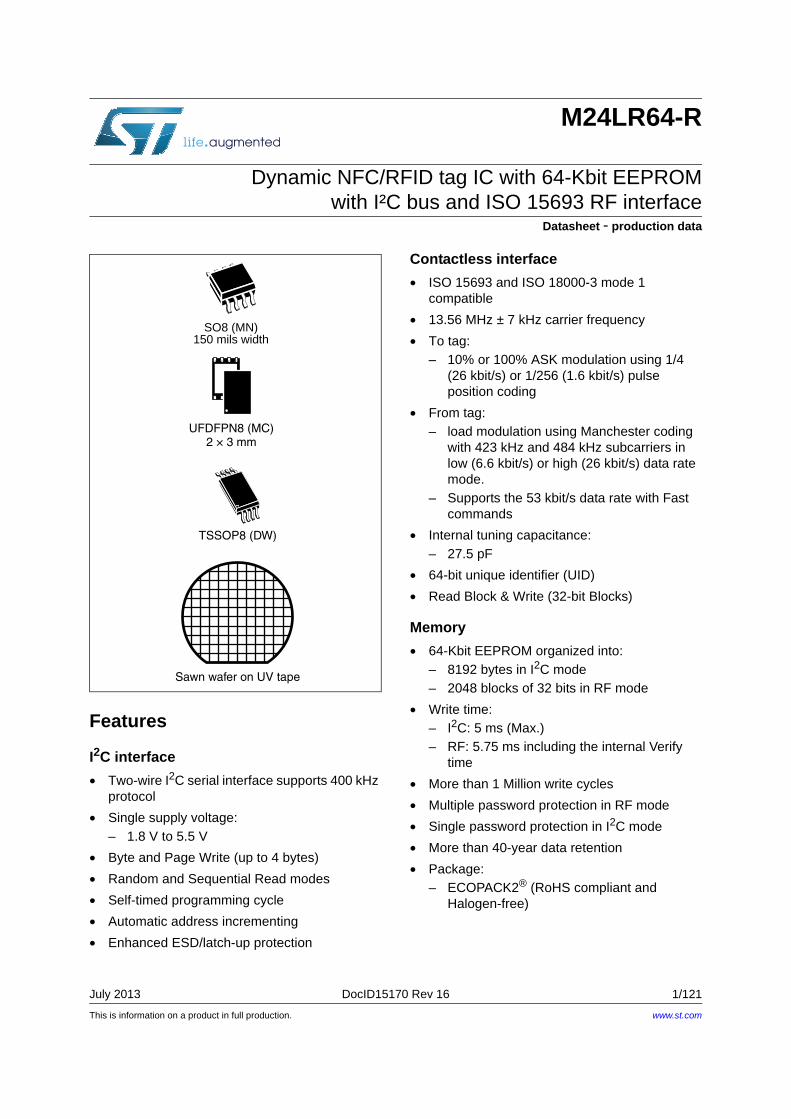
SO8 (MN)150 mils width
UFDFPN8 (MC)
TSSOP8 (DW)
Sawn wafer on UV tape
2 × 3 mm
www.st.com
Contents M24LR64-R
2/121 DocID15170 Rev 16
Contents
1 Description . . . . . . . . . . . . . . . . . . . . . . . . . . . . . . . . . . . . . . . . . . . . . . . . 12
2 Signal description . . . . . . . . . . . . . . . . . . . . . . . . . . . . . . . . . . . . . . . . . . 14
2.1 Serial Clock (SCL) . . . . . . . . . . . . . . . . . . . . . . . . . . . . . . . . . . . . . . . . . . 14
2.2 Serial Data (SDA) . . . . . . . . . . . . . . . . . . . . . . . . . . . . . . . . . . . . . . . . . . . 14
2.3 Chip Enable (E0, E1) . . . . . . . . . . . . . . . . . . . . . . . . . . . . . . . . . . . . . . . . 14
2.4 Antenna coil (AC0, AC1) . . . . . . . . . . . . . . . . . . . . . . . . . . . . . . . . . . . . . 14
2.5 VSS ground . . . . . . . . . . . . . . . . . . . . . . . . . . . . . . . . . . . . . . . . . . . . . . . . 15
2.6 Supply voltage (VCC) . . . . . . . . . . . . . . . . . . . . . . . . . . . . . . . . . . . . . . . . 15
2.6.1 Operating supply voltage VCC . . . . . . . . . . . . . . . . . . . . . . . . . . . . . . . . . . . . . . . . . 15
2.6.2 Power-up conditions . . . . . . . . . . . . . . . . . . . . . . . . . . . . . . . . . . . . . . . 15
2.6.3 Device reset . . . . . . . . . . . . . . . . . . . . . . . . . . . . . . . . . . . . . . . . . . . . . . 15
2.6.4 Power-down conditions . . . . . . . . . . . . . . . . . . . . . . . . . . . . . . . . . . . . . 15
3 User memory organization . . . . . . . . . . . . . . . . . . . . . . . . . . . . . . . . . . . 18
4 System memory area . . . . . . . . . . . . . . . . . . . . . . . . . . . . . . . . . . . . . . . 23
4.1 M24LR64-R RF block security . . . . . . . . . . . . . . . . . . . . . . . . . . . . . . . . . 23
4.2 Example of the M24LR64-R security protection . . . . . . . . . . . . . . . . . . . . 25
4.3 I2C_Write_Lock bit area . . . . . . . . . . . . . . . . . . . . . . . . . . . . . . . . . . . . . . 26
4.4 System parameters . . . . . . . . . . . . . . . . . . . . . . . . . . . . . . . . . . . . . . . . . 26
4.5 M24LR64-R I2C password security . . . . . . . . . . . . . . . . . . . . . . . . . . . . . 27
4.5.1 I2C Present Password command description . . . . . . . . . . . . . . . . . . . . 27
4.5.2 I2C Write Password command description . . . . . . . . . . . . . . . . . . . . . . 28
5 I2C device operation . . . . . . . . . . . . . . . . . . . . . . . . . . . . . . . . . . . . . . . . 30
5.1 Start condition . . . . . . . . . . . . . . . . . . . . . . . . . . . . . . . . . . . . . . . . . . . . . . 30
5.2 Stop condition . . . . . . . . . . . . . . . . . . . . . . . . . . . . . . . . . . . . . . . . . . . . . . 30
5.3 Acknowledge bit (ACK) . . . . . . . . . . . . . . . . . . . . . . . . . . . . . . . . . . . . . . 30
5.4 Data Input . . . . . . . . . . . . . . . . . . . . . . . . . . . . . . . . . . . . . . . . . . . . . . . . . 30
5.5 Memory addressing . . . . . . . . . . . . . . . . . . . . . . . . . . . . . . . . . . . . . . . . . 30
5.6 Write operations . . . . . . . . . . . . . . . . . . . . . . . . . . . . . . . . . . . . . . . . . . . . 31
5.7 Byte Write . . . . . . . . . . . . . . . . . . . . . . . . . . . . . . . . . . . . . . . . . . . . . . . . . 32
DocID15170 Rev 16 3/121
M24LR64-R Contents
5.8 Page Write . . . . . . . . . . . . . . . . . . . . . . . . . . . . . . . . . . . . . . . . . . . . . . . . 32
5.9 Minimizing system delays by polling on ACK . . . . . . . . . . . . . . . . . . . . . . 34
5.10 Read operations . . . . . . . . . . . . . . . . . . . . . . . . . . . . . . . . . . . . . . . . . . . . 35
5.11 Random Address Read . . . . . . . . . . . . . . . . . . . . . . . . . . . . . . . . . . . . . . 35
5.12 Current Address Read . . . . . . . . . . . . . . . . . . . . . . . . . . . . . . . . . . . . . . . 36
5.13 Sequential Read . . . . . . . . . . . . . . . . . . . . . . . . . . . . . . . . . . . . . . . . . . . . 36
5.14 Acknowledge in Read mode . . . . . . . . . . . . . . . . . . . . . . . . . . . . . . . . . . . 36
6 User memory initial state . . . . . . . . . . . . . . . . . . . . . . . . . . . . . . . . . . . . 37
7 RF device operation . . . . . . . . . . . . . . . . . . . . . . . . . . . . . . . . . . . . . . . . 37
7.1 Commands . . . . . . . . . . . . . . . . . . . . . . . . . . . . . . . . . . . . . . . . . . . . . . . . 38
7.2 Initial dialog for vicinity cards . . . . . . . . . . . . . . . . . . . . . . . . . . . . . . . . . . 38
7.2.1 Power transfer . . . . . . . . . . . . . . . . . . . . . . . . . . . . . . . . . . . . . . . . . . . . 39
7.2.2 Frequency . . . . . . . . . . . . . . . . . . . . . . . . . . . . . . . . . . . . . . . . . . . . . . . 39
7.2.3 Operating field . . . . . . . . . . . . . . . . . . . . . . . . . . . . . . . . . . . . . . . . . . . . 39
8 Communication signal from VCD to M24LR64-R . . . . . . . . . . . . . . . . . 40
9 Data rate and data coding . . . . . . . . . . . . . . . . . . . . . . . . . . . . . . . . . . . . 42
9.1 Data coding mode: 1 out of 256 . . . . . . . . . . . . . . . . . . . . . . . . . . . . . . . . 42
9.2 Data coding mode: 1 out of 4 . . . . . . . . . . . . . . . . . . . . . . . . . . . . . . . . . . 43
9.3 VCD to M24LR64-R frames . . . . . . . . . . . . . . . . . . . . . . . . . . . . . . . . . . . 45
9.4 Start of frame (SOF) . . . . . . . . . . . . . . . . . . . . . . . . . . . . . . . . . . . . . . . . . 45
10 Communications signal from M24LR64-R to VCD . . . . . . . . . . . . . . . . 47
10.1 Load modulation . . . . . . . . . . . . . . . . . . . . . . . . . . . . . . . . . . . . . . . . . . . . 47
10.2 Subcarrier . . . . . . . . . . . . . . . . . . . . . . . . . . . . . . . . . . . . . . . . . . . . . . . . . 47
10.3 Data rates . . . . . . . . . . . . . . . . . . . . . . . . . . . . . . . . . . . . . . . . . . . . . . . . . 47
11 Bit representation and coding . . . . . . . . . . . . . . . . . . . . . . . . . . . . . . . . 48
11.1 Bit coding using one subcarrier . . . . . . . . . . . . . . . . . . . . . . . . . . . . . . . . 48
11.1.1 High data rate . . . . . . . . . . . . . . . . . . . . . . . . . . . . . . . . . . . . . . . . . . . . 48
11.1.2 Low data rate . . . . . . . . . . . . . . . . . . . . . . . . . . . . . . . . . . . . . . . . . . . . . 49
11.2 Bit coding using two subcarriers . . . . . . . . . . . . . . . . . . . . . . . . . . . . . . . . 49
11.3 High data rate . . . . . . . . . . . . . . . . . . . . . . . . . . . . . . . . . . . . . . . . . . . . . . 49

Contents M24LR64-R
4/121 DocID15170 Rev 16
11.4 Low data rate . . . . . . . . . . . . . . . . . . . . . . . . . . . . . . . . . . . . . . . . . . . . . . 50
12 M24LR64-R to VCD frames . . . . . . . . . . . . . . . . . . . . . . . . . . . . . . . . . . . 51
12.1 SOF when using one subcarrier . . . . . . . . . . . . . . . . . . . . . . . . . . . . . . . . 51
12.2 High data rate . . . . . . . . . . . . . . . . . . . . . . . . . . . . . . . . . . . . . . . . . . . . . . 51
12.3 Low data rate . . . . . . . . . . . . . . . . . . . . . . . . . . . . . . . . . . . . . . . . . . . . . . 51
12.4 SOF when using two subcarriers . . . . . . . . . . . . . . . . . . . . . . . . . . . . . . . 52
12.5 High data rate . . . . . . . . . . . . . . . . . . . . . . . . . . . . . . . . . . . . . . . . . . . . . . 52
12.6 Low data rate . . . . . . . . . . . . . . . . . . . . . . . . . . . . . . . . . . . . . . . . . . . . . . 52
12.7 EOF when using one subcarrier . . . . . . . . . . . . . . . . . . . . . . . . . . . . . . . . 53
12.8 High data rate . . . . . . . . . . . . . . . . . . . . . . . . . . . . . . . . . . . . . . . . . . . . . . 53
12.9 Low data rate . . . . . . . . . . . . . . . . . . . . . . . . . . . . . . . . . . . . . . . . . . . . . . 53
12.10 EOF when using two subcarriers . . . . . . . . . . . . . . . . . . . . . . . . . . . . . . . 54
12.11 High data rate . . . . . . . . . . . . . . . . . . . . . . . . . . . . . . . . . . . . . . . . . . . . . . 54
12.12 Low data rate . . . . . . . . . . . . . . . . . . . . . . . . . . . . . . . . . . . . . . . . . . . . . . 54
13 Unique identifier (UID) . . . . . . . . . . . . . . . . . . . . . . . . . . . . . . . . . . . . . . 55
14 Application family identifier (AFI) . . . . . . . . . . . . . . . . . . . . . . . . . . . . . 56
15 Data storage format identifier (DSFID) . . . . . . . . . . . . . . . . . . . . . . . . . 57
15.1 CRC . . . . . . . . . . . . . . . . . . . . . . . . . . . . . . . . . . . . . . . . . . . . . . . . . . . . . 57
16 M24LR64-R protocol description . . . . . . . . . . . . . . . . . . . . . . . . . . . . . . 58
17 M24LR64-R states . . . . . . . . . . . . . . . . . . . . . . . . . . . . . . . . . . . . . . . . . . 60
17.1 Power-off state . . . . . . . . . . . . . . . . . . . . . . . . . . . . . . . . . . . . . . . . . . . . . 60
17.2 Ready state . . . . . . . . . . . . . . . . . . . . . . . . . . . . . . . . . . . . . . . . . . . . . . . 60
17.3 Quiet state . . . . . . . . . . . . . . . . . . . . . . . . . . . . . . . . . . . . . . . . . . . . . . . . 60
17.4 Selected state . . . . . . . . . . . . . . . . . . . . . . . . . . . . . . . . . . . . . . . . . . . . . . 60
18 Modes . . . . . . . . . . . . . . . . . . . . . . . . . . . . . . . . . . . . . . . . . . . . . . . . . . . . 62
18.1 Addressed mode . . . . . . . . . . . . . . . . . . . . . . . . . . . . . . . . . . . . . . . . . . . 62
18.2 Non-addressed mode (general request) . . . . . . . . . . . . . . . . . . . . . . . . . 62
18.3 Select mode . . . . . . . . . . . . . . . . . . . . . . . . . . . . . . . . . . . . . . . . . . . . . . . 62
DocID15170 Rev 16 5/121
M24LR64-R Contents
19 Request format . . . . . . . . . . . . . . . . . . . . . . . . . . . . . . . . . . . . . . . . . . . . 63
19.1 Request flags . . . . . . . . . . . . . . . . . . . . . . . . . . . . . . . . . . . . . . . . . . . . . . 63
20 Response format . . . . . . . . . . . . . . . . . . . . . . . . . . . . . . . . . . . . . . . . . . . 65
20.1 Response flags . . . . . . . . . . . . . . . . . . . . . . . . . . . . . . . . . . . . . . . . . . . . . 65
20.2 Response error code . . . . . . . . . . . . . . . . . . . . . . . . . . . . . . . . . . . . . . . . 66
21 Anticollision . . . . . . . . . . . . . . . . . . . . . . . . . . . . . . . . . . . . . . . . . . . . . . . 67
21.1 Request parameters . . . . . . . . . . . . . . . . . . . . . . . . . . . . . . . . . . . . . . . . . 67
22 Request processing by the M24LR64-R . . . . . . . . . . . . . . . . . . . . . . . . 69
23 Explanation of the possible cases . . . . . . . . . . . . . . . . . . . . . . . . . . . . . 70
24 Inventory Initiated command . . . . . . . . . . . . . . . . . . . . . . . . . . . . . . . . . 72
25 Timing definition . . . . . . . . . . . . . . . . . . . . . . . . . . . . . . . . . . . . . . . . . . . 73
25.1 t1: M24LR64-R response delay . . . . . . . . . . . . . . . . . . . . . . . . . . . . . . . . 73
25.2 t2: VCD new request delay . . . . . . . . . . . . . . . . . . . . . . . . . . . . . . . . . . . . 73
25.3 t3: VCD new request delay in the absence of a response fromthe M24LR64-R . . . . . . . . . . . . . . . . . . . . . . . . . . . . . . . . . . . . . . . . . . . . 73
26 Commands codes . . . . . . . . . . . . . . . . . . . . . . . . . . . . . . . . . . . . . . . . . . 74
26.1 Inventory . . . . . . . . . . . . . . . . . . . . . . . . . . . . . . . . . . . . . . . . . . . . . . . . . 74
26.2 Stay Quiet . . . . . . . . . . . . . . . . . . . . . . . . . . . . . . . . . . . . . . . . . . . . . . . . . 75
26.3 Read Single Block . . . . . . . . . . . . . . . . . . . . . . . . . . . . . . . . . . . . . . . . . . 76
26.4 Write Single Block . . . . . . . . . . . . . . . . . . . . . . . . . . . . . . . . . . . . . . . . . . 77
26.5 Read Multiple Block . . . . . . . . . . . . . . . . . . . . . . . . . . . . . . . . . . . . . . . . . 78
26.6 Select . . . . . . . . . . . . . . . . . . . . . . . . . . . . . . . . . . . . . . . . . . . . . . . . . . . . 80
26.7 Reset to Ready . . . . . . . . . . . . . . . . . . . . . . . . . . . . . . . . . . . . . . . . . . . . . 81
26.8 Write AFI . . . . . . . . . . . . . . . . . . . . . . . . . . . . . . . . . . . . . . . . . . . . . . . . . 82
26.9 Lock AFI . . . . . . . . . . . . . . . . . . . . . . . . . . . . . . . . . . . . . . . . . . . . . . . . . . 83
26.10 Write DSFID . . . . . . . . . . . . . . . . . . . . . . . . . . . . . . . . . . . . . . . . . . . . . . . 85
26.11 Lock DSFID . . . . . . . . . . . . . . . . . . . . . . . . . . . . . . . . . . . . . . . . . . . . . . . 87
26.12 Get System Info . . . . . . . . . . . . . . . . . . . . . . . . . . . . . . . . . . . . . . . . . . . . 88
26.13 Get Multiple Block Security Status . . . . . . . . . . . . . . . . . . . . . . . . . . . . . . 89
Contents M24LR64-R
6/121 DocID15170 Rev 16
26.14 Write-sector Password . . . . . . . . . . . . . . . . . . . . . . . . . . . . . . . . . . . . . . . 91
26.15 Lock-sector Password . . . . . . . . . . . . . . . . . . . . . . . . . . . . . . . . . . . . . . . 92
26.16 Present-sector Password . . . . . . . . . . . . . . . . . . . . . . . . . . . . . . . . . . . . . 94
26.17 Fast Read Single Block . . . . . . . . . . . . . . . . . . . . . . . . . . . . . . . . . . . . . . 95
26.18 Fast Inventory Initiated . . . . . . . . . . . . . . . . . . . . . . . . . . . . . . . . . . . . . . . 97
26.19 Fast Initiate . . . . . . . . . . . . . . . . . . . . . . . . . . . . . . . . . . . . . . . . . . . . . . . . 98
26.20 Fast Read Multiple Block . . . . . . . . . . . . . . . . . . . . . . . . . . . . . . . . . . . . . 99
26.21 Inventory Initiated . . . . . . . . . . . . . . . . . . . . . . . . . . . . . . . . . . . . . . . . . . 101
26.22 Initiate . . . . . . . . . . . . . . . . . . . . . . . . . . . . . . . . . . . . . . . . . . . . . . . . . . . 102
27 Maximum rating . . . . . . . . . . . . . . . . . . . . . . . . . . . . . . . . . . . . . . . . . . . 104
28 I2C DC and AC parameters . . . . . . . . . . . . . . . . . . . . . . . . . . . . . . . . . . 105
29 RF electrical parameters . . . . . . . . . . . . . . . . . . . . . . . . . . . . . . . . . . . . 109
30 Package mechanical data . . . . . . . . . . . . . . . . . . . . . . . . . . . . . . . . . . . 111
31 Part numbering . . . . . . . . . . . . . . . . . . . . . . . . . . . . . . . . . . . . . . . . . . . 114
Appendix A Anticollision algorithm (informative) . . . . . . . . . . . . . . . . . . . . . . . 116
A.1 Algorithm for pulsed slots . . . . . . . . . . . . . . . . . . . . . . . . . . . . . . . . . . . . .116
Appendix B CRC (informative) . . . . . . . . . . . . . . . . . . . . . . . . . . . . . . . . . . . . . . 117
B.1 CRC error detection method . . . . . . . . . . . . . . . . . . . . . . . . . . . . . . . . . . .117
B.2 CRC calculation example . . . . . . . . . . . . . . . . . . . . . . . . . . . . . . . . . . . . .117
Appendix C Application family identifier (AFI) (informative) . . . . . . . . . . . . . . 119
Revision history . . . . . . . . . . . . . . . . . . . . . . . . . . . . . . . . . . . . . . . . . . . . . . . . . . . 120
DocID15170 Rev 16 7/121
M24LR64-R List of tables
List of tables
Table 1. Signal names . . . . . . . . . . . . . . . . . . . . . . . . . . . . . . . . . . . . . . . . . . . . . . . . . . . . . . . . . . . 13Table 2. Device select code . . . . . . . . . . . . . . . . . . . . . . . . . . . . . . . . . . . . . . . . . . . . . . . . . . . . . . . 17Table 3. Address most significant byte . . . . . . . . . . . . . . . . . . . . . . . . . . . . . . . . . . . . . . . . . . . . . . . 17Table 4. Address least significant byte . . . . . . . . . . . . . . . . . . . . . . . . . . . . . . . . . . . . . . . . . . . . . . . 17Table 5. Sector details . . . . . . . . . . . . . . . . . . . . . . . . . . . . . . . . . . . . . . . . . . . . . . . . . . . . . . . . . . . 20Table 6. Sector Security Status Byte area . . . . . . . . . . . . . . . . . . . . . . . . . . . . . . . . . . . . . . . . . . . . 23Table 7. Sector security status byte organization . . . . . . . . . . . . . . . . . . . . . . . . . . . . . . . . . . . . . . . 23Table 8. Read / Write protection bit setting. . . . . . . . . . . . . . . . . . . . . . . . . . . . . . . . . . . . . . . . . . . . 24Table 9. Password Control bits . . . . . . . . . . . . . . . . . . . . . . . . . . . . . . . . . . . . . . . . . . . . . . . . . . . . . 24Table 10. Password system area . . . . . . . . . . . . . . . . . . . . . . . . . . . . . . . . . . . . . . . . . . . . . . . . . . . . 24Table 11. M24LR64-R sector security protection after power-up . . . . . . . . . . . . . . . . . . . . . . . . . . . . 25Table 12. M24LR64-R sector security protection after a valid presentation of password 1 . . . . . . . . 26Table 13. I2C_Write_Lock bit . . . . . . . . . . . . . . . . . . . . . . . . . . . . . . . . . . . . . . . . . . . . . . . . . . . . . . . 26Table 14. System parameter sector . . . . . . . . . . . . . . . . . . . . . . . . . . . . . . . . . . . . . . . . . . . . . . . . . . 27Table 15. Operating modes . . . . . . . . . . . . . . . . . . . . . . . . . . . . . . . . . . . . . . . . . . . . . . . . . . . . . . . . 31Table 16. 10% modulation parameters. . . . . . . . . . . . . . . . . . . . . . . . . . . . . . . . . . . . . . . . . . . . . . . . 40Table 17. Response data rates. . . . . . . . . . . . . . . . . . . . . . . . . . . . . . . . . . . . . . . . . . . . . . . . . . . . . . 47Table 18. UID format . . . . . . . . . . . . . . . . . . . . . . . . . . . . . . . . . . . . . . . . . . . . . . . . . . . . . . . . . . . . . 55Table 19. CRC transmission rules . . . . . . . . . . . . . . . . . . . . . . . . . . . . . . . . . . . . . . . . . . . . . . . . . . . 57Table 20. VCD request frame format . . . . . . . . . . . . . . . . . . . . . . . . . . . . . . . . . . . . . . . . . . . . . . . . . 58Table 21. M24LR64-R Response frame format . . . . . . . . . . . . . . . . . . . . . . . . . . . . . . . . . . . . . . . . . 58Table 22. M24LR64-R response depending on Request_flags . . . . . . . . . . . . . . . . . . . . . . . . . . . . . 61Table 23. General request format . . . . . . . . . . . . . . . . . . . . . . . . . . . . . . . . . . . . . . . . . . . . . . . . . . . . 63Table 24. Definition of request flags 1 to 4 . . . . . . . . . . . . . . . . . . . . . . . . . . . . . . . . . . . . . . . . . . . . . 63Table 25. Request flags 5 to 8 when Bit 3 = 0 . . . . . . . . . . . . . . . . . . . . . . . . . . . . . . . . . . . . . . . . . . 64Table 26. Request flags 5 to 8 when Bit 3 = 1 . . . . . . . . . . . . . . . . . . . . . . . . . . . . . . . . . . . . . . . . . . 64Table 27. General response format . . . . . . . . . . . . . . . . . . . . . . . . . . . . . . . . . . . . . . . . . . . . . . . . . . 65Table 28. Definitions of response flags 1 to 8. . . . . . . . . . . . . . . . . . . . . . . . . . . . . . . . . . . . . . . . . . . 65Table 29. Response error code definition. . . . . . . . . . . . . . . . . . . . . . . . . . . . . . . . . . . . . . . . . . . . . . 66Table 30. Inventory request format . . . . . . . . . . . . . . . . . . . . . . . . . . . . . . . . . . . . . . . . . . . . . . . . . . . 67Table 31. Example of the addition of 0 bits to an 11-bit mask value . . . . . . . . . . . . . . . . . . . . . . . . . 67Table 32. Timing values . . . . . . . . . . . . . . . . . . . . . . . . . . . . . . . . . . . . . . . . . . . . . . . . . . . . . . . . . . . 73Table 33. Command codes. . . . . . . . . . . . . . . . . . . . . . . . . . . . . . . . . . . . . . . . . . . . . . . . . . . . . . . . . 74Table 34. Inventory request format . . . . . . . . . . . . . . . . . . . . . . . . . . . . . . . . . . . . . . . . . . . . . . . . . . . 74Table 35. Inventory response format . . . . . . . . . . . . . . . . . . . . . . . . . . . . . . . . . . . . . . . . . . . . . . . . . 75Table 36. Stay Quiet request format . . . . . . . . . . . . . . . . . . . . . . . . . . . . . . . . . . . . . . . . . . . . . . . . . . 75Table 37. Read Single Block request format . . . . . . . . . . . . . . . . . . . . . . . . . . . . . . . . . . . . . . . . . . . 76Table 38. Read Single Block response format when Error_flag is NOT set . . . . . . . . . . . . . . . . . . . . 76Table 39. Sector security status . . . . . . . . . . . . . . . . . . . . . . . . . . . . . . . . . . . . . . . . . . . . . . . . . . . . . 76Table 40. Read Single Block response format when Error_flag is set . . . . . . . . . . . . . . . . . . . . . . . . 77Table 41. Write Single Block request format . . . . . . . . . . . . . . . . . . . . . . . . . . . . . . . . . . . . . . . . . . . 77Table 42. Write Single Block response format when Error_flag is NOT set . . . . . . . . . . . . . . . . . . . . 78Table 43. Write Single Block response format when Error_flag is set . . . . . . . . . . . . . . . . . . . . . . . . 78Table 44. Read Multiple Block request format . . . . . . . . . . . . . . . . . . . . . . . . . . . . . . . . . . . . . . . . . . 79Table 45. Read Multiple Block response format when Error_flag is NOT set. . . . . . . . . . . . . . . . . . . 79Table 46. Sector security status . . . . . . . . . . . . . . . . . . . . . . . . . . . . . . . . . . . . . . . . . . . . . . . . . . . . . 79Table 47. Read Multiple Block response format when Error_flag is set . . . . . . . . . . . . . . . . . . . . . . . 79Table 48. Select request format . . . . . . . . . . . . . . . . . . . . . . . . . . . . . . . . . . . . . . . . . . . . . . . . . . . . . 80

List of tables M24LR64-R
8/121 DocID15170 Rev 16
Table 49. Select Block response format when Error_flag is NOT set. . . . . . . . . . . . . . . . . . . . . . . . . 80Table 50. Select response format when Error_flag is set . . . . . . . . . . . . . . . . . . . . . . . . . . . . . . . . . . 80Table 51. Reset to Ready request format . . . . . . . . . . . . . . . . . . . . . . . . . . . . . . . . . . . . . . . . . . . . . . 81Table 52. Reset to Ready response format when Error_flag is NOT set . . . . . . . . . . . . . . . . . . . . . . 81Table 53. Reset to ready response format when Error_flag is set . . . . . . . . . . . . . . . . . . . . . . . . . . . 81Table 54. Write AFI request format. . . . . . . . . . . . . . . . . . . . . . . . . . . . . . . . . . . . . . . . . . . . . . . . . . . 82Table 55. Write AFI response format when Error_flag is NOT set . . . . . . . . . . . . . . . . . . . . . . . . . . . 82Table 56. Write AFI response format when Error_flag is set . . . . . . . . . . . . . . . . . . . . . . . . . . . . . . . 83Table 57. Lock AFI request format . . . . . . . . . . . . . . . . . . . . . . . . . . . . . . . . . . . . . . . . . . . . . . . . . . . 83Table 58. Lock AFI response format when Error_flag is NOT set . . . . . . . . . . . . . . . . . . . . . . . . . . . 84Table 59. Lock AFI response format when Error_flag is set . . . . . . . . . . . . . . . . . . . . . . . . . . . . . . . . 84Table 60. Write DSFID request format . . . . . . . . . . . . . . . . . . . . . . . . . . . . . . . . . . . . . . . . . . . . . . . . 85Table 61. Write DSFID response format when Error_flag is NOT set . . . . . . . . . . . . . . . . . . . . . . . . 85Table 62. Write DSFID response format when Error_flag is set . . . . . . . . . . . . . . . . . . . . . . . . . . . . . 85Table 63. Lock DSFID request format . . . . . . . . . . . . . . . . . . . . . . . . . . . . . . . . . . . . . . . . . . . . . . . . 87Table 64. Lock DSFID response format when Error_flag is NOT set . . . . . . . . . . . . . . . . . . . . . . . . . 87Table 65. Lock DSFID response format when Error_flag is set . . . . . . . . . . . . . . . . . . . . . . . . . . . . . 87Table 66. Get System Info request format . . . . . . . . . . . . . . . . . . . . . . . . . . . . . . . . . . . . . . . . . . . . . 88Table 67. Get System Info response format when Error_flag is NOT set. . . . . . . . . . . . . . . . . . . . . . 88Table 68. Get System Info response format when Error_flag is set . . . . . . . . . . . . . . . . . . . . . . . . . . 89Table 69. Get Multiple Block Security Status request format . . . . . . . . . . . . . . . . . . . . . . . . . . . . . . . 89Table 70. Get Multiple Block Security Status response format when Error_flag is NOT set . . . . . . . 90Table 71. Sector security status . . . . . . . . . . . . . . . . . . . . . . . . . . . . . . . . . . . . . . . . . . . . . . . . . . . . . 90Table 72. Get Multiple Block Security Status response format when Error_flag is set . . . . . . . . . . . . 90Table 73. Write-sector Password request format . . . . . . . . . . . . . . . . . . . . . . . . . . . . . . . . . . . . . . . . 91Table 74. Write-sector Password response format when Error_flag is NOT set . . . . . . . . . . . . . . . . 91Table 75. Write-sector Password response format when Error_flag is set . . . . . . . . . . . . . . . . . . . . . 91Table 76. Lock-sector Password request format . . . . . . . . . . . . . . . . . . . . . . . . . . . . . . . . . . . . . . . . 92Table 77. Sector security status . . . . . . . . . . . . . . . . . . . . . . . . . . . . . . . . . . . . . . . . . . . . . . . . . . . . . 93Table 78. Lock-sector Password response format when Error_flag is NOT set . . . . . . . . . . . . . . . . . 93Table 79. Lock-sector Password response format when Error_flag is set . . . . . . . . . . . . . . . . . . . . . 93Table 80. Present-sector Password request format . . . . . . . . . . . . . . . . . . . . . . . . . . . . . . . . . . . . . . 94Table 81. Present-sector Password response format when Error_flag is NOT set . . . . . . . . . . . . . . 94Table 82. Present-sector Password response format when Error_flag is set . . . . . . . . . . . . . . . . . . . 94Table 83. Fast Read Single Block request format . . . . . . . . . . . . . . . . . . . . . . . . . . . . . . . . . . . . . . . 95Table 84. Fast Read Single Block response format when Error_flag is NOT set . . . . . . . . . . . . . . . . 95Table 85. Sector security status . . . . . . . . . . . . . . . . . . . . . . . . . . . . . . . . . . . . . . . . . . . . . . . . . . . . . 96Table 86. Fast Read Single Block response format when Error_flag is set . . . . . . . . . . . . . . . . . . . . 96Table 87. Fast Inventory Initiated request format . . . . . . . . . . . . . . . . . . . . . . . . . . . . . . . . . . . . . . . . 97Table 88. Fast Inventory Initiated response format . . . . . . . . . . . . . . . . . . . . . . . . . . . . . . . . . . . . . . 97Table 89. Fast Initiate request format . . . . . . . . . . . . . . . . . . . . . . . . . . . . . . . . . . . . . . . . . . . . . . . . . 98Table 90. Fast Initiate response format . . . . . . . . . . . . . . . . . . . . . . . . . . . . . . . . . . . . . . . . . . . . . . . 98Table 91. Fast Read Multiple Block request format . . . . . . . . . . . . . . . . . . . . . . . . . . . . . . . . . . . . . . 99Table 92. Fast Read Multiple Block response format when Error_flag is NOT set. . . . . . . . . . . . . . . 99Table 93. Sector security status if Option_flag is set . . . . . . . . . . . . . . . . . . . . . . . . . . . . . . . . . . . . . 99Table 94. Fast Read Multiple Block response format when Error_flag is set . . . . . . . . . . . . . . . . . . 100Table 95. Inventory Initiated request format . . . . . . . . . . . . . . . . . . . . . . . . . . . . . . . . . . . . . . . . . . . 101Table 96. Inventory Initiated response format . . . . . . . . . . . . . . . . . . . . . . . . . . . . . . . . . . . . . . . . . 101Table 97. Initiate request format . . . . . . . . . . . . . . . . . . . . . . . . . . . . . . . . . . . . . . . . . . . . . . . . . . . . 102Table 98. Initiate Initiated response format. . . . . . . . . . . . . . . . . . . . . . . . . . . . . . . . . . . . . . . . . . . . 102Table 99. Absolute maximum ratings . . . . . . . . . . . . . . . . . . . . . . . . . . . . . . . . . . . . . . . . . . . . . . . . 104Table 100. I2C operating conditions . . . . . . . . . . . . . . . . . . . . . . . . . . . . . . . . . . . . . . . . . . . . . . . . . . 105

DocID15170 Rev 16 9/121
M24LR64-R List of tables
Table 101. AC test measurement conditions . . . . . . . . . . . . . . . . . . . . . . . . . . . . . . . . . . . . . . . . . . . 105Table 102. Input parameters. . . . . . . . . . . . . . . . . . . . . . . . . . . . . . . . . . . . . . . . . . . . . . . . . . . . . . . . 105Table 103. I2C DC characteristics . . . . . . . . . . . . . . . . . . . . . . . . . . . . . . . . . . . . . . . . . . . . . . . . . . . 106Table 104. I2C AC characteristics. . . . . . . . . . . . . . . . . . . . . . . . . . . . . . . . . . . . . . . . . . . . . . . . . . . . 107Table 105. RF characteristics . . . . . . . . . . . . . . . . . . . . . . . . . . . . . . . . . . . . . . . . . . . . . . . . . . . . . . 109Table 106. Operating conditions. . . . . . . . . . . . . . . . . . . . . . . . . . . . . . . . . . . . . . . . . . . . . . . . . . . . . 110Table 107. SO8N – 8-lead plastic small outline, 150 mils body width, package data. . . . . . . . . . . . . 111Table 108. UFDFPN8 (MLP8) – Ultra thin fine pitch dual flat package no lead 2 x 3 mm,
package mechanical data . . . . . . . . . . . . . . . . . . . . . . . . . . . . . . . . . . . . . . . . . . . . . . . . . 112Table 109. TSSOP8 – 8-lead thin shrink small outline, package mechanical data. . . . . . . . . . . . . . . 113Table 110. Ordering information scheme for packaged devices . . . . . . . . . . . . . . . . . . . . . . . . . . . . 114Table 111. Ordering information scheme for bare die devices . . . . . . . . . . . . . . . . . . . . . . . . . . . . . . 115Table 112. CRC definition. . . . . . . . . . . . . . . . . . . . . . . . . . . . . . . . . . . . . . . . . . . . . . . . . . . . . . . . . . 117Table 113. AFI coding. . . . . . . . . . . . . . . . . . . . . . . . . . . . . . . . . . . . . . . . . . . . . . . . . . . . . . . . . . . . . 119Table 114. Document revision history . . . . . . . . . . . . . . . . . . . . . . . . . . . . . . . . . . . . . . . . . . . . . . . . 120

List of figures M24LR64-R
10/121 DocID15170 Rev 16
List of figures
Figure 1. Logic diagram . . . . . . . . . . . . . . . . . . . . . . . . . . . . . . . . . . . . . . . . . . . . . . . . . . . . . . . . . . . 12Figure 2. 8-pin package connections . . . . . . . . . . . . . . . . . . . . . . . . . . . . . . . . . . . . . . . . . . . . . . . . . 13Figure 3. Device select code . . . . . . . . . . . . . . . . . . . . . . . . . . . . . . . . . . . . . . . . . . . . . . . . . . . . . . . 14Figure 4. I2C Fast mode (fC = 400 kHz): maximum Rbus value versus bus parasitic
capacitance (Cbus) . . . . . . . . . . . . . . . . . . . . . . . . . . . . . . . . . . . . . . . . . . . . . . . . . . . . . . . 16Figure 5. I2C bus protocol . . . . . . . . . . . . . . . . . . . . . . . . . . . . . . . . . . . . . . . . . . . . . . . . . . . . . . . . . 16Figure 6. Block diagram . . . . . . . . . . . . . . . . . . . . . . . . . . . . . . . . . . . . . . . . . . . . . . . . . . . . . . . . . . . 18Figure 7. Memory sector organization . . . . . . . . . . . . . . . . . . . . . . . . . . . . . . . . . . . . . . . . . . . . . . . . 19Figure 8. I2C Present Password command . . . . . . . . . . . . . . . . . . . . . . . . . . . . . . . . . . . . . . . . . . . . 28Figure 9. I2C Write Password command . . . . . . . . . . . . . . . . . . . . . . . . . . . . . . . . . . . . . . . . . . . . . . 29Figure 10. Write mode sequences with I2C_Write_Lock bit = 1 (data write inhibited). . . . . . . . . . . . . 31Figure 11. Write mode sequences with I2C_Write_Lock bit = 0 (data write enabled) . . . . . . . . . . . . . 33Figure 12. Write cycle polling flowchart using ACK . . . . . . . . . . . . . . . . . . . . . . . . . . . . . . . . . . . . . . . 33Figure 13. Read mode sequences. . . . . . . . . . . . . . . . . . . . . . . . . . . . . . . . . . . . . . . . . . . . . . . . . . . . 35Figure 14. 100% modulation waveform . . . . . . . . . . . . . . . . . . . . . . . . . . . . . . . . . . . . . . . . . . . . . . . . 40Figure 15. 10% modulation waveform . . . . . . . . . . . . . . . . . . . . . . . . . . . . . . . . . . . . . . . . . . . . . . . . . 41Figure 16. 1 out of 256 coding mode . . . . . . . . . . . . . . . . . . . . . . . . . . . . . . . . . . . . . . . . . . . . . . . . . . 42Figure 17. Detail of a time period. . . . . . . . . . . . . . . . . . . . . . . . . . . . . . . . . . . . . . . . . . . . . . . . . . . . . 43Figure 18. 1 out of 4 coding mode . . . . . . . . . . . . . . . . . . . . . . . . . . . . . . . . . . . . . . . . . . . . . . . . . . . . 44Figure 19. 1 out of 4 coding example. . . . . . . . . . . . . . . . . . . . . . . . . . . . . . . . . . . . . . . . . . . . . . . . . . 44Figure 20. SOF to select 1 out of 256 data coding mode . . . . . . . . . . . . . . . . . . . . . . . . . . . . . . . . . . 45Figure 21. SOF to select 1 out of 4 data coding mode . . . . . . . . . . . . . . . . . . . . . . . . . . . . . . . . . . . . 45Figure 22. EOF for either data coding mode . . . . . . . . . . . . . . . . . . . . . . . . . . . . . . . . . . . . . . . . . . . . 46Figure 23. Logic 0, high data rate . . . . . . . . . . . . . . . . . . . . . . . . . . . . . . . . . . . . . . . . . . . . . . . . . . . . 48Figure 24. Logic 0, high data rate x2 . . . . . . . . . . . . . . . . . . . . . . . . . . . . . . . . . . . . . . . . . . . . . . . . . . 48Figure 25. Logic 1, high data rate . . . . . . . . . . . . . . . . . . . . . . . . . . . . . . . . . . . . . . . . . . . . . . . . . . . . 48Figure 26. Logic 1, high data rate x2 . . . . . . . . . . . . . . . . . . . . . . . . . . . . . . . . . . . . . . . . . . . . . . . . . . 48Figure 27. Logic 0, low data rate . . . . . . . . . . . . . . . . . . . . . . . . . . . . . . . . . . . . . . . . . . . . . . . . . . . . . 49Figure 28. Logic 0, low data rate x2. . . . . . . . . . . . . . . . . . . . . . . . . . . . . . . . . . . . . . . . . . . . . . . . . . . 49Figure 29. Logic 1, low data rate . . . . . . . . . . . . . . . . . . . . . . . . . . . . . . . . . . . . . . . . . . . . . . . . . . . . . 49Figure 30. Logic 1, low data rate x2. . . . . . . . . . . . . . . . . . . . . . . . . . . . . . . . . . . . . . . . . . . . . . . . . . . 49Figure 31. Logic 0, high data rate . . . . . . . . . . . . . . . . . . . . . . . . . . . . . . . . . . . . . . . . . . . . . . . . . . . . 50Figure 32. Logic 1, high data rate . . . . . . . . . . . . . . . . . . . . . . . . . . . . . . . . . . . . . . . . . . . . . . . . . . . . 50Figure 33. Logic 0, low data rate . . . . . . . . . . . . . . . . . . . . . . . . . . . . . . . . . . . . . . . . . . . . . . . . . . . . . 50Figure 34. Logic 1, low data rate . . . . . . . . . . . . . . . . . . . . . . . . . . . . . . . . . . . . . . . . . . . . . . . . . . . . . 50Figure 35. Start of frame, high data rate, one subcarrier . . . . . . . . . . . . . . . . . . . . . . . . . . . . . . . . . . . 51Figure 36. Start of frame, high data rate, one subcarrier x2 . . . . . . . . . . . . . . . . . . . . . . . . . . . . . . . . 51Figure 37. Start of frame, low data rate, one subcarrier . . . . . . . . . . . . . . . . . . . . . . . . . . . . . . . . . . . 51Figure 38. Start of frame, low data rate, one subcarrier x2 . . . . . . . . . . . . . . . . . . . . . . . . . . . . . . . . . 52Figure 39. Start of frame, high data rate, two subcarriers . . . . . . . . . . . . . . . . . . . . . . . . . . . . . . . . . . 52Figure 40. Start of frame, low data rate, two subcarriers . . . . . . . . . . . . . . . . . . . . . . . . . . . . . . . . . . . 52Figure 41. End of frame, high data rate, one subcarriers . . . . . . . . . . . . . . . . . . . . . . . . . . . . . . . . . . 53Figure 42. End of frame, high data rate, one subcarriers x2 . . . . . . . . . . . . . . . . . . . . . . . . . . . . . . . . 53Figure 43. End of frame, low data rate, one subcarriers . . . . . . . . . . . . . . . . . . . . . . . . . . . . . . . . . . . 53Figure 44. End of frame, low data rate, one subcarriers x2 . . . . . . . . . . . . . . . . . . . . . . . . . . . . . . . . . 53Figure 45. End of frame, high data rate, two subcarriers . . . . . . . . . . . . . . . . . . . . . . . . . . . . . . . . . . . 54Figure 46. End of frame, low data rate, two subcarriers . . . . . . . . . . . . . . . . . . . . . . . . . . . . . . . . . . . 54Figure 47. M24LR64-R decision tree for AFI . . . . . . . . . . . . . . . . . . . . . . . . . . . . . . . . . . . . . . . . . . . . 56
DocID15170 Rev 16 11/121
M24LR64-R List of figures
Figure 48. M24LR64-R protocol timing . . . . . . . . . . . . . . . . . . . . . . . . . . . . . . . . . . . . . . . . . . . . . . . . 59Figure 49. M24LR64-R state transition diagram . . . . . . . . . . . . . . . . . . . . . . . . . . . . . . . . . . . . . . . . . 61Figure 50. Principle of comparison between the mask, the slot number and the UID . . . . . . . . . . . . . 68Figure 51. Description of a possible anticollision sequence . . . . . . . . . . . . . . . . . . . . . . . . . . . . . . . . 71Figure 52. Stay Quiet frame exchange between VCD and M24LR64-R . . . . . . . . . . . . . . . . . . . . . . . 76Figure 53. Read Single Block frame exchange between VCD and M24LR64-R . . . . . . . . . . . . . . . . . 77Figure 54. Write Single Block frame exchange between VCD and M24LR64-R . . . . . . . . . . . . . . . . . 78Figure 55. Read Multiple Block frame exchange between VCD and M24LR64-R. . . . . . . . . . . . . . . . 80Figure 56. Select frame exchange between VCD and M24LR64-R . . . . . . . . . . . . . . . . . . . . . . . . . . 81Figure 57. Reset to Ready frame exchange between VCD and M24LR64-R . . . . . . . . . . . . . . . . . . . 82Figure 58. Write AFI frame exchange between VCD and M24LR64-R . . . . . . . . . . . . . . . . . . . . . . . . 83Figure 59. Lock AFI frame exchange between VCD and M24LR64-R . . . . . . . . . . . . . . . . . . . . . . . . 84Figure 60. Write DSFID frame exchange between VCD and M24LR64-R . . . . . . . . . . . . . . . . . . . . . 86Figure 61. Lock DSFID frame exchange between VCD and M24LR64-R . . . . . . . . . . . . . . . . . . . . . . 88Figure 62. Get System Info frame exchange between VCD and M24LR64-R. . . . . . . . . . . . . . . . . . . 89Figure 63. Get Multiple Block Security Status frame exchange between VCD and M24LR64-R . . . . 90Figure 64. Write-sector Password frame exchange between VCD and M24LR64-R . . . . . . . . . . . . . 92Figure 65. Lock-sector Password frame exchange between VCD and M24LR64-R . . . . . . . . . . . . . . 93Figure 66. Present-sector Password frame exchange between VCD and M24LR64-R . . . . . . . . . . . 95Figure 67. Fast Read Single Block frame exchange between VCD and M24LR64-R . . . . . . . . . . . . . 96Figure 68. Fast Initiate frame exchange between VCD and M24LR64-R . . . . . . . . . . . . . . . . . . . . . . 98Figure 69. Fast Read Multiple Block frame exchange between VCD and M24LR64-R. . . . . . . . . . . 100Figure 70. Initiate frame exchange between VCD and M24LR64-R . . . . . . . . . . . . . . . . . . . . . . . . . 103Figure 71. AC test measurement I/O waveform. . . . . . . . . . . . . . . . . . . . . . . . . . . . . . . . . . . . . . . . . 105Figure 72. I2C AC waveforms . . . . . . . . . . . . . . . . . . . . . . . . . . . . . . . . . . . . . . . . . . . . . . . . . . . . . . 108Figure 73. M24LR64-R synchronous timing, transmit and receive . . . . . . . . . . . . . . . . . . . . . . . . . . 110Figure 74. SO8N – 8-lead plastic small outline, 150 mils body width, package outline . . . . . . . . . . . 111Figure 75. UFDFPN8 (MLP8) – Ultra thin fine pitch dual flat package no lead 2 x 3 mm,
package outline. . . . . . . . . . . . . . . . . . . . . . . . . . . . . . . . . . . . . . . . . . . . . . . . . . . . . . . . . 112Figure 76. TSSOP8 – 8-lead thin shrink small outline, package outline . . . . . . . . . . . . . . . . . . . . . . 113
Description M24LR64-R
12/121 DocID15170 Rev 16
1 Description
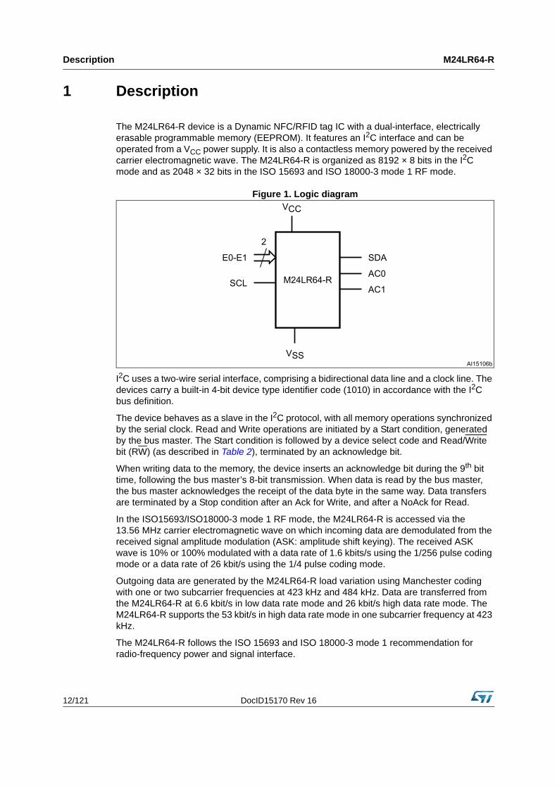
The M24LR64-R device is a Dynamic NFC/RFID tag IC with a dual-interface, electrically erasable programmable memory (EEPROM). It features an I2C interface and can be operated from a VCC power supply. It is also a contactless memory powered by the received carrier electromagnetic wave. The M24LR64-R is organized as 8192 × 8 bits in the I2C mode and as 2048 × 32 bits in the ISO 15693 and ISO 18000-3 mode 1 RF mode.
Figure 1. Logic diagram
I2C uses a two-wire serial interface, comprising a bidirectional data line and a clock line. The devices carry a built-in 4-bit device type identifier code (1010) in accordance with the I2C bus definition.
The device behaves as a slave in the I2C protocol, with all memory operations synchronized by the serial clock. Read and Write operations are initiated by a Start condition, generated by the bus master. The Start condition is followed by a device select code and Read/Write bit (RW) (as described in Table 2), terminated by an acknowledge bit.
When writing data to the memory, the device inserts an acknowledge bit during the 9th bit time, following the bus master’s 8-bit transmission. When data is read by the bus master, the bus master acknowledges the receipt of the data byte in the same way. Data transfers are terminated by a Stop condition after an Ack for Write, and after a NoAck for Read.
In the ISO15693/ISO18000-3 mode 1 RF mode, the M24LR64-R is accessed via the 13.56 MHz carrier electromagnetic wave on which incoming data are demodulated from the received signal amplitude modulation (ASK: amplitude shift keying). The received ASK wave is 10% or 100% modulated with a data rate of 1.6 kbits/s using the 1/256 pulse coding mode or a data rate of 26 kbit/s using the 1/4 pulse coding mode.
Outgoing data are generated by the M24LR64-R load variation using Manchester coding with one or two subcarrier frequencies at 423 kHz and 484 kHz. Data are transferred from the M24LR64-R at 6.6 kbit/s in low data rate mode and 26 kbit/s high data rate mode. The M24LR64-R supports the 53 kbit/s in high data rate mode in one subcarrier frequency at 423 kHz.
The M24LR64-R follows the ISO 15693 and ISO 18000-3 mode 1 recommendation for radio-frequency power and signal interface.
AI15106b
2
E0-E1 SDA
VCC
M24LR64-RSCL
VSS
AC0
AC1
DocID15170 Rev 16 13/121
M24LR64-R Description
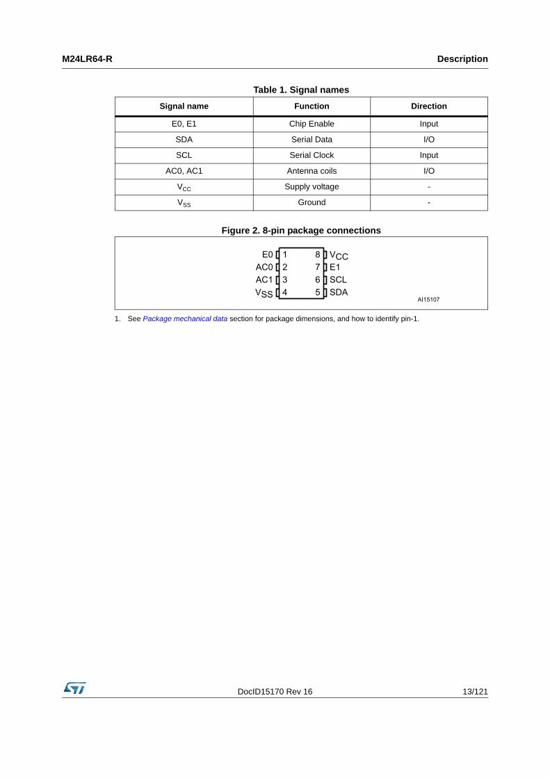
Figure 2. 8-pin package connections
1. See Package mechanical data section for package dimensions, and how to identify pin-1.
Table 1. Signal names
Signal name Function Direction
E0, E1 Chip Enable Input
SDA Serial Data I/O
SCL Serial Clock Input
AC0, AC1 Antenna coils I/O
VCC Supply voltage -
VSS Ground -
SDAVSS
SCLE1AC0
E0 VCC
AC1
AI15107
1234
8765
Signal description M24LR64-R
14/121 DocID15170 Rev 16
2 Signal description
2.1 Serial Clock (SCL)
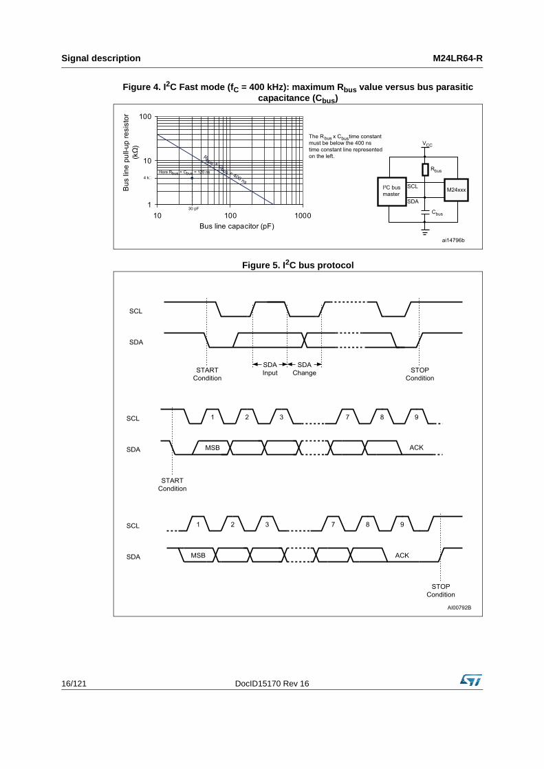
This input signal is used to strobe all data in and out of the device. In applications where this signal is used by slave devices to synchronize the bus to a slower clock, the bus master must have an open drain output, and a pull-up resistor must be connected from Serial Clock (SCL) to VCC. (Figure 4 indicates how the value of the pull-up resistor can be calculated). In most applications, though, this method of synchronization is not employed, and so the pull-up resistor is not necessary, provided that the bus master has a push-pull (rather than open drain) output.
2.2 Serial Data (SDA)
This bidirectional signal is used to transfer data in or out of the device. It is an open drain output that may be wire-OR’ed with other open drain or open collector signals on the bus. A pull up resistor must be connected from Serial Data (SDA) to VCC. (Figure 4 indicates how the value of the pull-up resistor can be calculated).
2.3 Chip Enable (E0, E1)
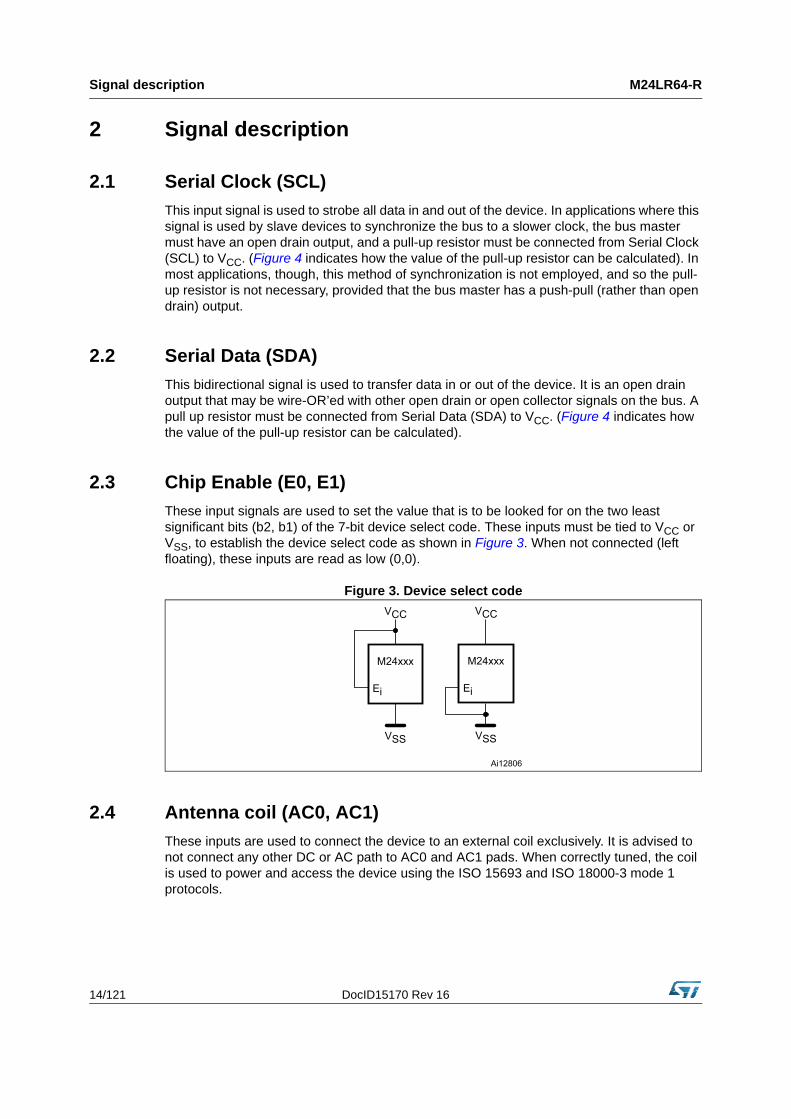
These input signals are used to set the value that is to be looked for on the two least significant bits (b2, b1) of the 7-bit device select code. These inputs must be tied to VCC or VSS, to establish the device select code as shown in Figure 3. When not connected (left floating), these inputs are read as low (0,0).
Figure 3. Device select code
2.4 Antenna coil (AC0, AC1)
These inputs are used to connect the device to an external coil exclusively. It is advised to not connect any other DC or AC path to AC0 and AC1 pads. When correctly tuned, the coil is used to power and access the device using the ISO 15693 and ISO 18000-3 mode 1 protocols.
Ai12806
VCC
M24xxx
VSS
Ei
VCC
M24xxx
VSS
Ei
DocID15170 Rev 16 15/121
M24LR64-R Signal description
2.5 VSS ground
VSS is the reference for the VCC supply voltage.
2.6 Supply voltage (VCC)
This pin can be connected to an external DC supply voltage.
Note: An internal voltage regulator allows the external voltage applied on VCC to supply the M24LR64-R, while preventing the internal power supply (rectified RF waveforms) to output a DC voltage on the VCC pin.
2.6.1 Operating supply voltage VCC
Prior to selecting the memory and issuing instructions to it, a valid and stable VCC voltage within the specified [VCC(min), VCC(max)] range must be applied (see Table 100). To maintain a stable DC supply voltage, it is recommended to decouple the VCC line with a suitable capacitor (usually of the order of 10 nF) close to the VCC/VSS package pins.
This voltage must remain stable and valid until the end of the transmission of the instruction and, for a Write instruction, until the completion of the internal I²C write cycle (tW).
2.6.2 Power-up conditions
When the power supply is turned on, VCC rises from VSS to VCC. The VCC rise time must not vary faster than 1V/µs.
2.6.3 Device reset
In order to prevent inadvertent write operations during power-up, a power-on reset (POR) circuit is included. At power-up (continuous rise of VCC), the device does not respond to any instruction until VCC has reached the power-on reset threshold voltage (this threshold is lower than the minimum VCC operating voltage defined in Table 100). When VCC passes over the POR threshold, the device is reset and enters the Standby Power mode, however, the device must not be accessed until VCC has reached a valid and stable VCC voltage within the specified [VCC(min), VCC(max)] range.
In a similar way, during power-down (continuous decrease in VCC), as soon as VCC drops below the power-on reset threshold voltage, the device stops responding to any instruction sent to it.
2.6.4 Power-down conditions
During power-down (continuous decay of VCC), the device must be in Standby Power mode (mode reached after decoding a Stop condition, assuming that there is no internal write cycle in progress).
Signal description M24LR64-R
16/121 DocID15170 Rev 16
Figure 4. I2C Fast mode (fC = 400 kHz): maximum Rbus value versus bus parasiticcapacitance (Cbus)
Figure 5. I2C bus protocol
ai14796b
1
10
100
10 100 1000Bus line capacitor (pF)
Bus
line
pul
l-up
resi
stor
(k
Ω)
I²C busmaster
M24xxx
Rbus
VCC
Cbus
SCL
SDA
Rbus × Cbus = 400 ns
Here Rbus × Cbus = 120 ns4 k�
30 pF
The R x C time constantmust be below the 400 nstime constant line representedon the left.
bus bus
SCL
SDA
SCL
SDA
SDA
STARTCondition
SDAInput
SDAChange
AI00792B
STOPCondition
1 2 3 7 8 9
MSB ACK
STARTCondition
SCL 1 2 3 7 8 9
MSB ACK
STOPCondition

DocID15170 Rev 16 17/121
M24LR64-R Signal description
Table 2. Device select code
Device type identifier(1)
1. The most significant bit, b7, is sent first.
Chip Enable address(2)
2. E0 and E1 are compared against the respective external pins on the memory device.
RW
b7 b6 b5 b4 b3 b2 b1 b0
Device select code 1 0 1 0 E2(3)
3. E2 is not connected to any external pin. It is however used to address the M24LR64-R as described in Section 3 and Section 4.
E1 E0 RW
Table 3. Address most significant byte
b15 b14 b13 b12 b11 b10 b9 b8
Table 4. Address least significant byte
b7 b6 b5 b4 b3 b2 b1 b0
User memory organization M24LR64-R
18/121 DocID15170 Rev 16
3 User memory organization
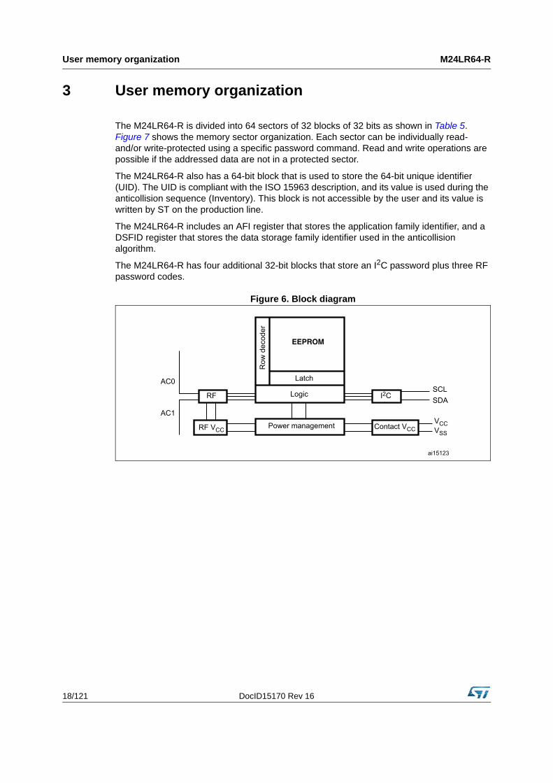
The M24LR64-R is divided into 64 sectors of 32 blocks of 32 bits as shown in Table 5. Figure 7 shows the memory sector organization. Each sector can be individually read- and/or write-protected using a specific password command. Read and write operations are possible if the addressed data are not in a protected sector.
The M24LR64-R also has a 64-bit block that is used to store the 64-bit unique identifier (UID). The UID is compliant with the ISO 15963 description, and its value is used during the anticollision sequence (Inventory). This block is not accessible by the user and its value is written by ST on the production line.
The M24LR64-R includes an AFI register that stores the application family identifier, and a DSFID register that stores the data storage family identifier used in the anticollision algorithm.
The M24LR64-R has four additional 32-bit blocks that store an I2C password plus three RF password codes.
Figure 6. Block diagram
EEPROM
Row
dec
oder
Latch
LogicRF I2C
RF VCC Contact VCC
SCLSDA
VSS
VCC
AC0
AC1
Power management
ai15123

DocID15170 Rev 16 19/121
M24LR64-R User memory organization
Figure 7. Memory sector organization
Sector details
The M24LR64-R user memory is divided into 64 sectors. Each sector contains 1024 bits. The protection scheme is described in Section 4: System memory area.
In RF mode, a sector provides 32 blocks of 32 bits. Each read and write access are done by block. Read and write block accesses are controlled by a Sector Security Status byte that defines the access rights to all the 32 blocks contained in the sector. If the sector is not protected, a Write command updates the complete 32 bits of the selected block.
In I2C mode, a sector provides 128 bytes that can be individually accessed in read and write modes. When protected by the corresponding I2C_Write_Lock bit, the entire sector is write-protected. To access the user memory, the device select code used for any I2C command must have the E2 Chip Enable address at 0.
0 1 Kbit EEPROM sector 5 bits
1 1 Kbit EEPROM sector 5 bits
2 1 Kbit EEPROM sector 5 bits
3 1 Kbit EEPROM sector 5 bits
60 1 Kbit EEPROM sector 5 bits
61 1 Kbit EEPROM sector 5 bits
62 1 Kbit EEPROM sector 5 bits
63 1 Kbit EEPROM sector 5 bits
I2C Password System
RF Password 1 System
RF Password 2 System
RF Password 3 System
8 bit DSFID System
8 bit AFI System
64 bit UID System
Sector Area Sector security status
ai15124

User memory organization M24LR64-R
20/121 DocID15170 Rev 16
Table 5. Sector details
Sector number
RF block address
I2C byte address
Bits [31:24] Bits [23:16] Bits [15:8] Bits [7:0]
0
0 0 user user user user
1 4 user user user user
2 8 user user user user
3 12 user user user user
4 16 user user user user
5 20 user user user user
6 24 user user user user
7 28 user user user user
8 32 user user user user
9 36 user user user user
10 40 user user user user
11 44 user user user user
12 48 user user user user
13 52 user user user user
14 56 user user user user
15 60 user user user user
16 64 user user user user
17 68 user user user user
18 72 user user user user
19 76 user user user user
20 80 user user user user
21 84 user user user user
22 88 user user user user
23 92 user user user user
24 96 user user user user
25 100 user user user user
26 104 user user user user
27 108 user user user user
28 112 user user user user
29 116 user user user user
30 120 user user user user
31 124 user user user user
DocID15170 Rev 16 21/121
M24LR64-R User memory organization
1
32 128 user user user user
33 132 user user user user
34 136 user user user user
35 140 user user user user
36 144 user user user user
37 148 user user user user
38 152 user user user user
39 156 user user user user
... ... ... ... ... ...
... ... ... ... ... ... ...
Table 5. Sector details (continued)
Sector number
RF block address
I2C byte address
Bits [31:24] Bits [23:16] Bits [15:8] Bits [7:0]
User memory organization M24LR64-R
22/121 DocID15170 Rev 16
63
2016 8064 user user user user
2017 8068 user user user user
2018 8072 user user user user
2019 8076 user user user user
2020 8080 user user user user
2021 8084 user user user user
2022 8088 user user user user
2023 8092 user user user user
2024 8096 user user user user
2025 8100 user user user user
2026 8104 user user user user
2027 8108 user user user user
2028 8112 user user user user
2029 8116 user user user user
2030 8120 user user user user
2031 8124 user user user user
2032 8128 user user user user
2033 8132 user user user user
2034 8136 user user user user
2035 8140 user user user user
2036 8144 user user user user
2037 8148 user user user user
2038 8152 user user user user
2039 8156 user user user user
2040 8160 user user user user
2041 8164 user user user user
2042 8168 user user user user
2043 8172 user user user user
2044 8176 user user user user
2045 8180 user user user user
2046 8184 user user user user
2047 8188 user user user user
Table 5. Sector details (continued)
Sector number
RF block address
I2C byte address
Bits [31:24] Bits [23:16] Bits [15:8] Bits [7:0]
DocID15170 Rev 16 23/121
M24LR64-R System memory area
4 System memory area
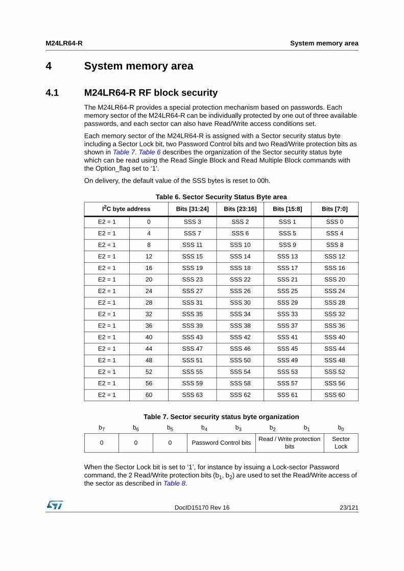
4.1 M24LR64-R RF block security
The M24LR64-R provides a special protection mechanism based on passwords. Each memory sector of the M24LR64-R can be individually protected by one out of three available passwords, and each sector can also have Read/Write access conditions set.
Each memory sector of the M24LR64-R is assigned with a Sector security status byte including a Sector Lock bit, two Password Control bits and two Read/Write protection bits as shown in Table 7. Table 6 describes the organization of the Sector security status byte which can be read using the Read Single Block and Read Multiple Block commands with the Option_flag set to ‘1’.
On delivery, the default value of the SSS bytes is reset to 00h.
When the Sector Lock bit is set to ‘1’, for instance by issuing a Lock-sector Password command, the 2 Read/Write protection bits (b1, b2) are used to set the Read/Write access of the sector as described in Table 8.
Table 6. Sector Security Status Byte area
I2C byte address Bits [31:24] Bits [23:16] Bits [15:8] Bits [7:0]
E2 = 1 0 SSS 3 SSS 2 SSS 1 SSS 0
E2 = 1 4 SSS 7 SSS 6 SSS 5 SSS 4
E2 = 1 8 SSS 11 SSS 10 SSS 9 SSS 8
E2 = 1 12 SSS 15 SSS 14 SSS 13 SSS 12
E2 = 1 16 SSS 19 SSS 18 SSS 17 SSS 16
E2 = 1 20 SSS 23 SSS 22 SSS 21 SSS 20
E2 = 1 24 SSS 27 SSS 26 SSS 25 SSS 24
E2 = 1 28 SSS 31 SSS 30 SSS 29 SSS 28
E2 = 1 32 SSS 35 SSS 34 SSS 33 SSS 32
E2 = 1 36 SSS 39 SSS 38 SSS 37 SSS 36
E2 = 1 40 SSS 43 SSS 42 SSS 41 SSS 40
E2 = 1 44 SSS 47 SSS 46 SSS 45 SSS 44
E2 = 1 48 SSS 51 SSS 50 SSS 49 SSS 48
E2 = 1 52 SSS 55 SSS 54 SSS 53 SSS 52
E2 = 1 56 SSS 59 SSS 58 SSS 57 SSS 56
E2 = 1 60 SSS 63 SSS 62 SSS 61 SSS 60
Table 7. Sector security status byte organization
b7 b6 b5 b4 b3 b2 b1 b0
0 0 0 Password Control bitsRead / Write protection
bitsSector Lock
System memory area M24LR64-R
24/121 DocID15170 Rev 16
The next 2 bits of the Sector security status byte (b3, b4) are the Password Control bits. The value these two bits is used to link a password to the sector as defined in Table 9.
The M24LR64-R password protection is organized around a dedicated set of commands plus a system area of three password blocks where the password values are stored. This system area is described in Table 10.
The dedicated password commands are:
• Write-sector Password:
The Write-sector Password command is used to write a 32-bit block into the password system area. This command must be used to update password values. After the write cycle, the new password value is automatically activated. It is possible to modify a password value after issuing a valid Present-sector Password command.On delivery, the three default password values are set to 0000 0000h and are activated.
• Lock-sector Password:
The Lock-sector Password command is used to set the Sector security status byte of the selected sector. Bits b4 to b1 of the Sector security status byte are affected by the Lock-sector Password command. The Sector Lock bit, b0, is set to ‘1’ automatically. After issuing a Lock-sector Password command, the protection settings of the selected
Table 8. Read / Write protection bit setting
Sector Lock
b2, b1Sector access when password
presentedSector access when password not
presented
0 xx Read Write Read Write
1 00 Read Write Read No Write
1 01 Read Write Read Write
1 10 Read Write No Read No Write
1 11 Read No Write No Read No Write
Table 9. Password Control bits
b4, b3 Password
00 The sector is not protected by a Password
01 The sector is protected by the Password 1
10 The sector is protected by the Password 2
11 The sector is protected by the Password 3
Table 10. Password system area
Block number 32-bit password number
1 Password 1
2 Password 2
3 Password 3

DocID15170 Rev 16 25/121
M24LR64-R System memory area
sector are activated. The protection of a locked block cannot be changed in RF mode. A Lock-sector Password command sent to a locked sector returns an error code.
• Present-sector Password:
The Present-sector Password command is used to present one of the three passwords to the M24LR64-R in order to modify the access rights of all the memory sectors linked to that password (Table 8) including the password itself. If the presented password is correct, the access rights remain activated until the tag is powered off or until a new Present-sector Password command is issued. If the presented password value is not correct, all the access rights of all the memory sectors are deactivated.
• Sector security status byte area access conditions in I2C mode:
In I2C mode, read access to the Sector security status byte area is always allowed. Write access depends on the correct presentation of the I2C password (see I2C Present Password command description on page 27).
To access the Sector security status byte area, the device select code used for any I2C command must have the E2 Chip Enable address at 1.
An I2C write access to a Sector security status byte re-initializes the RF access condition to the given memory sector.
4.2 Example of the M24LR64-R security protection
Table 11 and Table 12 show the sector security protections before and after a valid Present-sector Password command. Table 11 shows the sector access rights of an M24LR64-R after power-up. After a valid Present-sector Password command with password 1, the memory sector access is changed as shown in Table 12.
Table 11. M24LR64-R sector security protection after power-up
Sector address
Sector security status byte
b7b6b5 b4 b3 b2 b1 b0
0 Protection: Standard Read No Write xxx 0 0 0 0 1
1 Protection: Pswd 1 Read No Write xxx 0 1 0 0 1
2 Protection: Pswd 1 Read Write xxx 0 1 0 1 1
3 Protection: Pswd 1 No Read No Write xxx 0 1 1 0 1
4 Protection: Pswd 1 No Read No Write xxx 0 1 1 1 1

System memory area M24LR64-R
26/121 DocID15170 Rev 16
4.3 I2C_Write_Lock bit area
In the I2C mode only, it is possible to protect individual sectors against Write operations. This feature is controlled by the I2C_Write_Lock bits stored in the 8 bytes of the I2C_Write_Lock bit area starting from the location 2048 (see Table 13). Using these 64 bits, it is possible to write-protect all the 64 sectors of the M24LR64-R memory.
Each bit controls the I2C write access to a specific sector as shown in Table 13. It is always possible to unprotect a sector in the I2C mode. When an I2C_Write_Lock bit is reset to 0, the corresponding sector is unprotected. When the bit is set to 1, the corresponding sector is write-protected.
In I2C mode, read access to the I2C_Write_Lock bit area is always allowed. Write access depends on the correct presentation of the I2C password.
To access the I2C_Write_Lock bit area, the device select code used for any I2C command must have the E2 Chip Enable address at 1.
On delivery, the default value of the 8 bytes of the I2C_Write_Lock bit area is reset to 00h.
4.4 System parameters
The M24LR64-R provides the system area required by the ISO 15693 RF protocol, as shown in Table 14.
The first 32-bit block starting from I2C address 2304 stores the I2C password. This password is used to activate/deactivate the write protection of the protected sector in I2C mode. At power-on, all user memory sectors protected by the I2C_Write_Lock bits can be read but cannot be modified. To remove the write protection, it is necessary to use the I2C Present Password described in Figure 8. When the password is correctly presented — that is, when all the presented bits correspond to the stored ones — it is also possible to modify the I2C password using the I2C Write Password command described in Figure 9.
Table 12. M24LR64-R sector security protection after a valid presentation of password 1
Sector address
Sector security status byte
b7b6b5 b4 b3 b2 b1 b0
0 Protection: Standard Read No Write xxx 0 0 0 0 1
1 Protection: Pswd 1 Read Write xxx 0 1 0 0 1
2 Protection: Pswd 1 Read Write xxx 0 1 0 1 1
3 Protection: Pswd 1 Read Write xxx 0 1 1 0 1
4 Protection: Pswd 1 Read No Write xxx 0 1 1 1 1
Table 13. I2C_Write_Lock bit
I2C byte address Bits [31:24] Bits [23:16] Bits [15:8] Bits [7:0]
E2 = 1 2048 sectors 31-24 sectors 23-16 sectors 15-8 sectors 7-0
E2 = 1 2052 sectors 63-56 sectors 55-48 sectors 47-40 sectors 39-32

DocID15170 Rev 16 27/121
M24LR64-R System memory area
The next three 32-bit blocks store the three RF passwords. These passwords are neither read- nor write- accessible in the I2C mode.
The next 2 bytes are used to store the AFI, at I2C location 2322, and the DSFID, at I2C location 2323. These 2 values are used during the RF Inventory sequence. They are read-only in the I2C mode.
The next 8 bytes, starting from location 2324, store the 64-bit UID programmed by ST on the production line. Bytes at I2C locations 2332 to 2335 store the IC Ref and the Mem_Size data used by the RF Get_System_Info command. The UID, Mem_Size and IC Ref values are read-only data.
4.5 M24LR64-R I2C password security
The M24LR64-R controls I2C sector write access using the 32-bit-long I2C password and the 64-bit I2C_Write_Lock bit area. The I2C password value is managed using two I2C commands: I2C Present Password and I2C Write Password.
4.5.1 I2C Present Password command description
The I2C Present Password command is used in I2C mode to present the password to the M24LR64-R in order to modify the write access rights of all the memory sectors protected by the I2C_Write_Lock bits, including the password itself. If the presented password is correct, the access rights remain activated until the M24LR64-R is powered off or until a new I2C Present Password command is issued.
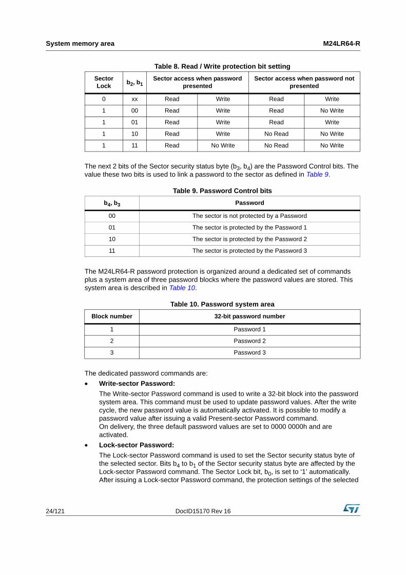
Following a Start condition, the bus master sends a device select code with the Read/Write bit (RW) reset to 0 and the Chip Enable bit E2 at 1. The device acknowledges this, as shown in Figure 8, and waits for two I2C password address bytes 09h and 00h. The device responds to each address byte with an acknowledge bit, and then waits for the 4 password data bytes, the validation code, 09h, and a resend of the 4 password data bytes. The most significant byte of the password is sent first, followed by the least significant bytes.
It is necessary to send the 32-bit password twice to prevent any data corruption during the sequence. If the two 32-bit passwords sent are not exactly the same, the M24LR64-R does not start the internal comparison.
Table 14. System parameter sector
I2C byte address Bits [31:24] Bits [23:16] Bits [15:8] Bits [7:0]
E2 = 1 2304 I2C password (1)
1. Delivery state: I2C password= 0000 0000h, RF password = 0000 0000h,
E2 = 1 2308 RF password 1(1)
E2 = 1 2312 RF password 2(1)
E2 = 1 2316 RF password 3 (1)
E2 = 1 2320 DSFID (FFh) AFI (00h) ST reserved ST reserved
E2 = 1 2324 UID UID UID UID
E2 = 1 2328 UID (E0h) UID (02h) UID UID
E2 = 1 2332 Mem_Size (03 07FFh) IC Ref (2Ch)
System memory area M24LR64-R
28/121 DocID15170 Rev 16
When the bus master generates a Stop condition immediately after the Ack bit (during the “10th bit” time slot), an internal delay equivalent to the write cycle time is triggered. A Stop condition at any other time does not trigger the internal delay. During that delay, the M24LR64-R compares the 32 received data bits with the 32 bits of the stored I2C password. If the values match, the write access rights to all protected sectors are modified after the internal delay. If the values do not match, the protected sectors remains protected.
During the internal delay, Serial Data (SDA) is disabled internally, and the device does not respond to any requests.
Figure 8. I2C Present Password command
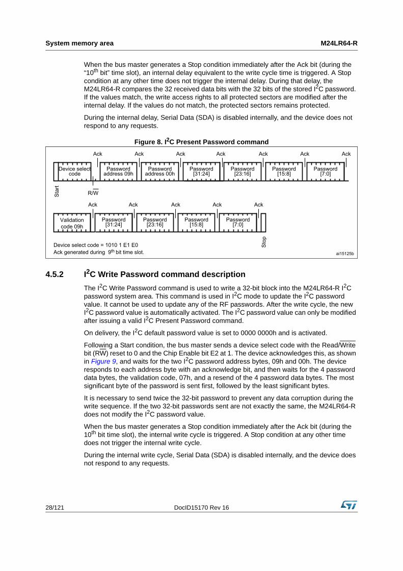
4.5.2 I2C Write Password command description
The I2C Write Password command is used to write a 32-bit block into the M24LR64-R I2C password system area. This command is used in I2C mode to update the I2C password value. It cannot be used to update any of the RF passwords. After the write cycle, the new I2C password value is automatically activated. The I2C password value can only be modified after issuing a valid I2C Present Password command.
On delivery, the I2C default password value is set to 0000 0000h and is activated.
Following a Start condition, the bus master sends a device select code with the Read/Write bit (RW) reset to 0 and the Chip Enable bit E2 at 1. The device acknowledges this, as shown in Figure 9, and waits for the two I2C password address bytes, 09h and 00h. The device responds to each address byte with an acknowledge bit, and then waits for the 4 password data bytes, the validation code, 07h, and a resend of the 4 password data bytes. The most significant byte of the password is sent first, followed by the least significant bytes.
It is necessary to send twice the 32-bit password to prevent any data corruption during the write sequence. If the two 32-bit passwords sent are not exactly the same, the M24LR64-R does not modify the I2C password value.
When the bus master generates a Stop condition immediately after the Ack bit (during the 10th bit time slot), the internal write cycle is triggered. A Stop condition at any other time does not trigger the internal write cycle.
During the internal write cycle, Serial Data (SDA) is disabled internally, and the device does not respond to any requests.
ai15125b
Sta
rt
Device selectcode
Passwordaddress 09h
Passwordaddress 00h
Password[31:24]
Ack
R/W
Ack Ack Ack
Device select code = 1010 1 E1 E0
Password[23:16]
Password[15:8]
Password[7:0]
Ack Ack Ack
Ack generated during 9th bit time slot.
Sto
p
Validationcode 09h
Ack
Password[31:24]
Ack
Password[23:16]
Password[15:8]
Password[7:0]
Ack Ack Ack

DocID15170 Rev 16 29/121
M24LR64-R System memory area
Figure 9. I2C Write Password command
ai15126
Sta
rt
Device selectcode
Passwordaddress 09h
Passwordaddress 00h
New password[31:24]
Ack
R/W
Ack Ack Ack
Device select code = 1010 1 E1 E0
New password[23:16]
New password[15:8]
New password[7:0]
Ack Ack Ack
Ack generated during 9th bit time slot.
Sto
p
Validationcode 07h
Ack
New password[31:24]
Ack
New password[23:16]
New password[15:8]
New password[7:0]
Ack Ack Ack
I2C device operation M24LR64-R
30/121 DocID15170 Rev 16
5 I2C device operation
The device supports the I2C protocol. This is summarized in Figure 5. Any device that sends data on to the bus is defined to be a transmitter, and any device that reads the data to be a receiver. The device that controls the data transfer is known as the bus master, and the other as the slave device. A data transfer can only be initiated by the bus master, which will also provide the serial clock for synchronization. The M24LR64-R device is always a slave in all communications.
5.1 Start condition
Start is identified by a falling edge of Serial Data (SDA) while Serial Clock (SCL) is stable in the high state. A Start condition must precede any data transfer command. The device continuously monitors (except during a write cycle) Serial Data (SDA) and Serial Clock (SCL) for a Start condition, and will not respond unless one is given.
5.2 Stop condition
Stop is identified by a rising edge of Serial Data (SDA) while Serial Clock (SCL) is stable and driven high. A Stop condition terminates communication between the device and the bus master. A Read command that is followed by NoAck can be followed by a Stop condition to force the device into the Standby mode. A Stop condition at the end of a Write command triggers the internal write cycle.
5.3 Acknowledge bit (ACK)
The acknowledge bit is used to indicate a successful byte transfer. The bus transmitter, whether it be bus master or slave device, releases Serial Data (SDA) after sending eight bits of data. During the 9th clock pulse period, the receiver pulls Serial Data (SDA) low to acknowledge the receipt of the eight data bits.
5.4 Data Input
During data input, the device samples Serial Data (SDA) on the rising edge of Serial Clock (SCL). For correct device operation, Serial Data (SDA) must be stable during the rising edge of Serial Clock (SCL), and the Serial Data (SDA) signal must change only when Serial Clock (SCL) is driven low.
5.5 Memory addressing
To start communication between the bus master and the slave device, the bus master must initiate a Start condition. Following this, the bus master sends the device select code, shown in Table 2 (on Serial Data (SDA), most significant bit first).
The device select code consists of a 4-bit device type identifier, and a 3-bit Chip Enable “Address” (E2, E1, E0). To address the memory array, the 4-bit device type identifier is 1010b.

DocID15170 Rev 16 31/121
M24LR64-R I2C device operation
Up to four memory devices can be connected on a single I2C bus. Each one is given a unique 2-bit code on the Chip Enable (E0, E1) inputs. When the device select code is received, the device only responds if the Chip Enable Address is the same as the value on the Chip Enable (E0, E1) inputs.
The 8th bit is the Read/Write bit (RW). This bit is set to 1 for Read and 0 for Write operations.
If a match occurs on the device select code, the corresponding device gives an acknowledgment on Serial Data (SDA) during the 9th bit time. If the device does not match the device select code, it deselects itself from the bus, and goes into Standby mode.
Figure 10. Write mode sequences with I2C_Write_Lock bit = 1 (data write inhibited)
5.6 Write operations
Following a Start condition the bus master sends a device select code with the Read/Write bit (RW) reset to 0. The device acknowledges this, as shown in Figure 11, and waits for two address bytes. The device responds to each address byte with an acknowledge bit, and then waits for the data byte.
Table 15. Operating modes
Mode RW bit Bytes Initial sequence
Current Address Read 1 1 Start, device select, RW = 1
Random Address Read0
1Start, device select, RW = 0, Address
1 reStart, device select, RW = 1
Sequential Read 1 ≥ 1 Similar to Current or Random Address Read
Byte Write 0 1 Start, device select, RW = 0
Page Write 0 ≤ 4 bytes Start, device select, RW = 0
Sto
p
Sta
rt
Byte Write Dev select Byte address Byte address Data in
Sta
rt
Page Write Dev select Byte address Byte address Data in 1 Data in 2
AI15115
Page Write(cont'd)
Sto
p
Data in N
ACK ACK ACK NO ACK
R/W
ACK ACK ACK NO ACK
R/W
NO ACK NO ACK
I2C device operation M24LR64-R
32/121 DocID15170 Rev 16
Writing to the memory may be inhibited if the I2C_Write_Lock bit = 1. A Write instruction issued with the I2C_Write_Lock bit = 1 and with no I2C_Password presented, does not modify the memory contents, and the accompanying data bytes are not acknowledged, as shown in Figure 10.
Each data byte in the memory has a 16-bit (two byte wide) address. The most significant byte (Table 3) is sent first, followed by the least significant byte (Table 4). Bits b15 to b0 form the address of the byte in memory.
When the bus master generates a Stop condition immediately after the Ack bit (in the “10th bit” time slot), either at the end of a Byte Write or a Page Write, the internal write cycle is triggered. A Stop condition at any other time slot does not trigger the internal write cycle.
After the Stop condition, the delay tW, and the successful completion of a Write operation, the device’s internal address counter is incremented automatically, to point to the next byte address after the last one that was modified.
During the internal write cycle, Serial Data (SDA) is disabled internally, and the device does not respond to any requests.
5.7 Byte Write
After the device select code and the address bytes, the bus master sends one data byte. If the addressed location is write-protected by the I2C_Write_Lock bit (= 1), the device replies with NoAck, and the location is not modified. If, instead, the addressed location is not Write-protected, the device replies with Ack. The bus master terminates the transfer by generating a Stop condition, as shown in Figure 11.
5.8 Page Write
The Page Write mode allows up to 4 bytes to be written in a single Write cycle, provided that they are all located in the same “row” in the memory: that is, the most significant memory address bits (b12-b2) are the same. If more bytes are sent than will fit up to the end of the row, a condition known as ‘roll-over’ occurs. This should be avoided, as data starts to become overwritten in an implementation dependent way.
The bus master sends from 1 to 4 bytes of data, each of which is acknowledged by the device if the I2C_Write_Lock bit = 0 or the I2C_Password was correctly presented. If the I2C_Write_Lock_bit = 1 and the I2C_password is not presented, the contents of the addressed memory location are not modified, and each data byte is followed by a NoAck. After each byte is transferred, the internal byte address counter (inside the page) is incremented. The transfer is terminated by the bus master generating a Stop condition.
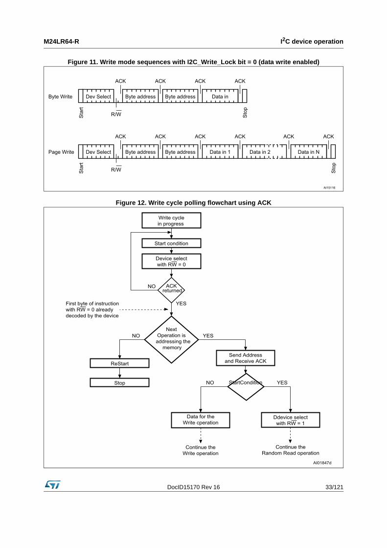
DocID15170 Rev 16 33/121
M24LR64-R I2C device operation
Figure 11. Write mode sequences with I2C_Write_Lock bit = 0 (data write enabled)
Figure 12. Write cycle polling flowchart using ACK
Sto
p
Sta
rt
Byte Write Dev Select Byte address Byte address Data in
Sta
rt
Page Write Dev Select Byte address Byte address Data in 1 Data in 2
AI15116
Sto
p
Data in N
ACK
R/W
ACK ACK ACK
ACK ACK ACK ACK
R/W
ACKACK
Write cyclein progress
AI01847d
NextOperation isaddressing the
memory
Start condition
Device selectwith RW = 0
ACKreturned
YES
NO
YESNO
ReStart
Stop
Data for theWrite cperation
Ddevice selectwith RW = 1
Send Addressand Receive ACK
First byte of instructionwith RW = 0 alreadydecoded by the device
YESNO StartCondition
Continue theWrite operation
Continue theRandom Read operation
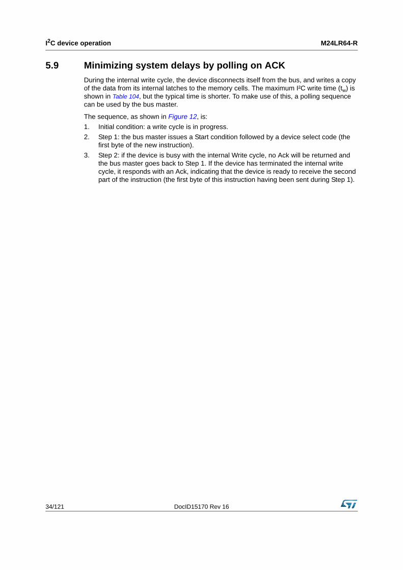
I2C device operation M24LR64-R
34/121 DocID15170 Rev 16
5.9 Minimizing system delays by polling on ACK
During the internal write cycle, the device disconnects itself from the bus, and writes a copy of the data from its internal latches to the memory cells. The maximum I²C write time (tw) is shown in Table 104, but the typical time is shorter. To make use of this, a polling sequence can be used by the bus master.
The sequence, as shown in Figure 12, is:
1. Initial condition: a write cycle is in progress.
2. Step 1: the bus master issues a Start condition followed by a device select code (the first byte of the new instruction).
3. Step 2: if the device is busy with the internal Write cycle, no Ack will be returned and the bus master goes back to Step 1. If the device has terminated the internal write cycle, it responds with an Ack, indicating that the device is ready to receive the second part of the instruction (the first byte of this instruction having been sent during Step 1).

DocID15170 Rev 16 35/121
M24LR64-R I2C device operation
Figure 13. Read mode sequences
1. The seven most significant bits of the device select code of a Random Read (in the 1st and 4th bytes) must be identical.
5.10 Read operations
Read operations are performed independently of the state of the I2C_Write_Lock bit.
After the successful completion of a Read operation, the device’s internal address counter is incremented by one, to point to the next byte address.
5.11 Random Address Read
A dummy Write is first performed to load the address into this address counter (as shown in Figure 13) but without sending a Stop condition. Then, the bus master sends another Start condition, and repeats the device select code, with the Read/Write bit (RW) set to 1. The
Sta
rtDev sel * Byte addr Byte addr
Sta
rt
Dev sel Data out 1
AI01105d
Data out N
Sto
p
Sta
rt
CurrentAddressRead
Dev sel Data out
RandomAddressRead
Sto
p
Sta
rt
Dev sel * Data out
SequentialCurrentRead
Sto
p
Data out N
Sta
rt
Dev sel * Byte addr Byte addrSequentionRandomRead
Sta
rtDev sel * Data out1
Sto
p
ACK
R/W
NO ACK
ACK
R/W
ACK ACK ACK
R/W
ACK ACK ACK NO ACK
R/W
NO ACK
ACK ACK ACK
R/W
ACK ACK
R/W
ACK NO ACK

I2C device operation M24LR64-R
36/121 DocID15170 Rev 16
device acknowledges this, and outputs the contents of the addressed byte. The bus master must not acknowledge the byte, and terminates the transfer with a Stop condition.
5.12 Current Address Read
For the Current Address Read operation, following a Start condition, the bus master only sends a device select code with the Read/Write bit (RW) set to 1. The device acknowledges this, and outputs the byte addressed by the internal address counter. The counter is then incremented. The bus master terminates the transfer with a Stop condition, as shown in Figure 13, without acknowledging the byte.
5.13 Sequential Read
This operation can be used after a Current Address Read or a Random Address Read. The bus master does acknowledge the data byte output, and sends additional clock pulses so that the device continues to output the next byte in sequence. To terminate the stream of bytes, the bus master must not acknowledge the last byte, and must generate a Stop condition, as shown in Figure 13.
The output data comes from consecutive addresses, with the internal address counter automatically incremented after each byte output. After the last memory address, the address counter ‘rolls-over’, and the device continues to output data from memory address 00h.
5.14 Acknowledge in Read mode
For all Read commands, the device waits, after each byte read, for an acknowledgment during the 9th bit time. If the bus master does not drive Serial Data (SDA) low during this time, the device terminates the data transfer and switches to its Standby mode.

DocID15170 Rev 16 37/121
M24LR64-R User memory initial state
6 User memory initial state
The device is delivered with all bits in the user memory array set to 1 (each byte contains FFh).
7 RF device operation
The M24LR64-R is divided into 64 sectors of 32 blocks of 32 bits as shown in Table 5. Each sector can be individually read- and/or write-protected using a specific lock or password command.
Read and Write operations are possible if the addressed block is not protected. During a Write, the 32 bits of the block are replaced by the new 32-bit value.
The M24LR64-R also has a 64-bit block that is used to store the 64-bit unique identifier (UID). The UID is compliant with the ISO 15963 description, and its value is used during the anticollision sequence (Inventory). This block is not accessible by the user and its value is written by ST on the production line.
The M24LR64-R also includes an AFI register in which the application family identifier is stored, and a DSFID register in which the data storage family identifier used in the anticollision algorithm is stored. The M24LR64-R has three additional 32-bit blocks in which the password codes are stored.

RF device operation M24LR64-R
38/121 DocID15170 Rev 16
7.1 Commands
The M24LR64-R supports the following commands:
• Inventory, used to perform the anticollision sequence.
• Stay Quiet, used to put the M24LR64-R in quiet mode, where it does not respond to any inventory command.
• Select, used to select the M24LR64-R. After this command, the M24LR64-R processes all Read/Write commands with Select_flag set.
• Reset To Ready, used to put the M24LR64-R in the ready state.
• Read Block, used to output the 32 bits of the selected block and its locking status.
• Write Block, used to write the 32-bit value in the selected block, provided that it is not locked.
• Read Multiple Blocks, used to read the selected blocks and send back their value.
• Write AFI, used to write the 8-bit value in the AFI register.
• Lock AFI, used to lock the AFI register.
• Write DSFID, used to write the 8-bit value in the DSFID register.
• Lock DSFID, used to lock the DSFID register.
• Get System Info, used to provide the system information value
• Get Multiple Block Security Status, used to send the security status of the selected block.
• Initiate, used to trigger the tag response to the Inventory Initiated sequence.
• Inventory Initiated, used to perform the anticollision sequence triggered by the Initiate command.
• Write-sector Password, used to write the 32 bits of the selected password.
• Lock-sector Password, used to write the Sector security status bits of the selected sector.
• Present-sector Password, enables the user to present a password to unprotect the user blocks linked to this password.
• Fast Initiate, used to trigger the tag response to the Inventory Initiated sequence.
• Fast Inventory Initiated, used to perform the anticollision sequence triggered by the Initiate command.
• Fast Read Single Block, used to output the 32 bits of the selected block and its locking status.
• Fast Read Multiple Blocks, used to read the selected blocks and send back their value.
7.2 Initial dialog for vicinity cards
The dialog between the vicinity coupling device or VCD (commonly the “RF reader”) and the vicinity integrated circuit card or VICC (M24LR64-R) takes place as follows:
• activation of the M24LR64-R by the RF operating field of the VCD
• transmission of a command by the VCD
• transmission of a response by the M24LR64-R
DocID15170 Rev 16 39/121
M24LR64-R RF device operation
These operations use the RF power transfer and communication signal interface described below (see Power transfer, Frequency and Operating field). This technique is called RTF (Reader Talk First).
7.2.1 Power transfer
Power is transferred to the M24LR64-R by radio frequency at 13.56 MHz via coupling antennas in the M24LR64-R and the VCD. The RF operating field of the VCD is transformed on the M24LR64-R antenna to an AC Voltage which is rectified, filtered and internally regulated. The amplitude modulation (ASK) on this received signal is demodulated by the ASK demodulator.
7.2.2 Frequency
The ISO 15693 standard defines the carrier frequency (fC) of the operating field as 13.56 MHz ±7 kHz.
7.2.3 Operating field
The M24LR64-R operates continuously between the minimum and maximum values of the electromagnetic field H defined in Table 105. The VCD has to generate a field within these limits.

Communication signal from VCD to M24LR64-R M24LR64-R
40/121 DocID15170 Rev 16
8 Communication signal from VCD to M24LR64-R
Communications between the VCD and the M24LR64-R takes place using the modulation principle of ASK (Amplitude Shift Keying). Two modulation indexes are used, 10% and 100%. The M24LR64-R decodes both. The VCD determines which index is used.
The modulation index is defined as [a – b]/[a + b] where a is the peak signal amplitude and b, the minimum signal amplitude of the carrier frequency.
Depending on the choice made by the VCD, a “pause” will be created as described in Figure 14 and Figure 15.
The M24LR64-R is operational for any degree of modulation index from between 10% and 30%.
Figure 14. 100% modulation waveform
Table 16. 10% modulation parameters
Symbol Parameter definition Value
hr 0.1 x (a – b) max
hf 0.1 x (a – b) max
105%a
95%
5%
60%
CarrierAmplitude
t
t2
t1 t3
t4
Min (μs)t1 6,0t2 2,1t3 0
Max (μs)9,44
t14,5
t4 0 0,8
b
The clock recovery shall be operational after t4 max.
ai15793

DocID15170 Rev 16 41/121
M24LR64-R Communication signal from VCD to M24LR64-R
Figure 15. 10% modulation waveform
The VICC shall be operational for any value of modulation index between 10 % and 30 %.
Min6,0 μs
t2 3,0 μst3 0
Max9,44 μs
t14,5 μs
ModulationIndex
t1
10% 30% hf, hr 0,1 (a-b) maxy 0,05 (a-b)
t1
t2
hfy
hr
t3
t
y
a
b
CarrierAmplitude
Min6,0 μs
t2 3,0 μst3 0
Max9,44 μs
t14,5 μs
ModulationIndex
t1
10% 30%
Min6,0 μs
t2 3,0 μst3 0
Max9,44 μs
t14,5 μs
ModulationIndex
t1
10% 30% hf, hr 0,1 (a-b) maxy 0,05 (a-b)
hf, hr 0,1 (a-b) maxy 0,05 (a-b)
t1
t2
hfy
hr
t3
t
y
a
b
CarrierAmplitude
ai15794

Data rate and data coding M24LR64-R
42/121 DocID15170 Rev 16
9 Data rate and data coding
The data coding implemented in the M24LR64-R uses pulse position modulation. Both data coding modes that are described in the ISO15693 are supported by the M24LR64-R. The selection is made by the VCD and indicated to the M24LR64-R within the start of frame (SOF).
9.1 Data coding mode: 1 out of 256
The value of one single byte is represented by the position of one pause. The position of the pause on 1 of 256 successive time periods of 18.88 µs (256/fC), determines the value of the byte. In this case the transmission of one byte takes 4.833 ms and the resulting data rate is 1.65 kbit/s (fC/8192).
Figure 16 illustrates this pulse position modulation technique. In this figure, data E1h (225 decimal) is sent by the VCD to the M24LR64-R.
The pause occurs during the second half of the position of the time period that determines the value, as shown in Figure 17.
A pause during the first period transmits the data value 00h. A pause during the last period transmit the data value FFh (255 decimal).
Figure 16. 1 out of 256 coding mode
AI06656
0 1 2 3 . . . . . . . . 2 . . . . . . . . . . . . . . . . . . . . . 2 2 2 2 . . . . . . . . . 2 . . . . . . . . . . . . . . . . . . . . . 5 5 5 5 . . . . . . . . . 5 . . . . . . . . . . . . . . . . . . . . . 2 3 4 5
4.833 ms
18.88 μs
9.44 μs
PulseModulatedCarrier

DocID15170 Rev 16 43/121
M24LR64-R Data rate and data coding
Figure 17. Detail of a time period
9.2 Data coding mode: 1 out of 4
The value of 2 bits is represented by the position of one pause. The position of the pause on 1 of 4 successive time periods of 18.88 µs (256/fC), determines the value of the 2 bits. Four successive pairs of bits form a byte, where the least significant pair of bits is transmitted first.
In this case the transmission of one byte takes 302.08 µs and the resulting data rate is 26.48 kbit/s (fC/512). Figure 18 illustrates the 1 out of 4 pulse position technique and coding. Figure 19 shows the transmission of E1h (225d - 1110 0001b) by the VCD.
AI06657
225
18.88 μs
9.44 μs
PulseModulatedCarrier
226
224
. . . . . . .. . . . . . .
Time Periodone of 256
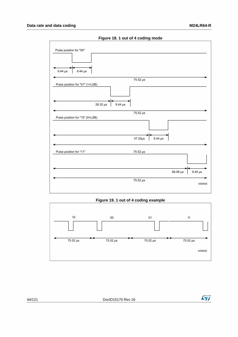
Data rate and data coding M24LR64-R
44/121 DocID15170 Rev 16
Figure 18. 1 out of 4 coding mode
Figure 19. 1 out of 4 coding example
AI06658
9.44 μs 9.44 μs
75.52 μs
28.32 μs 9.44 μs
75.52 μs
47.20μs 9.44 μs
75.52 μs
66.08 μs 9.44 μs
75.52 μs
Pulse position for "00"
Pulse position for "11"
Pulse position for "10" (0=LSB)
Pulse position for "01" (1=LSB)
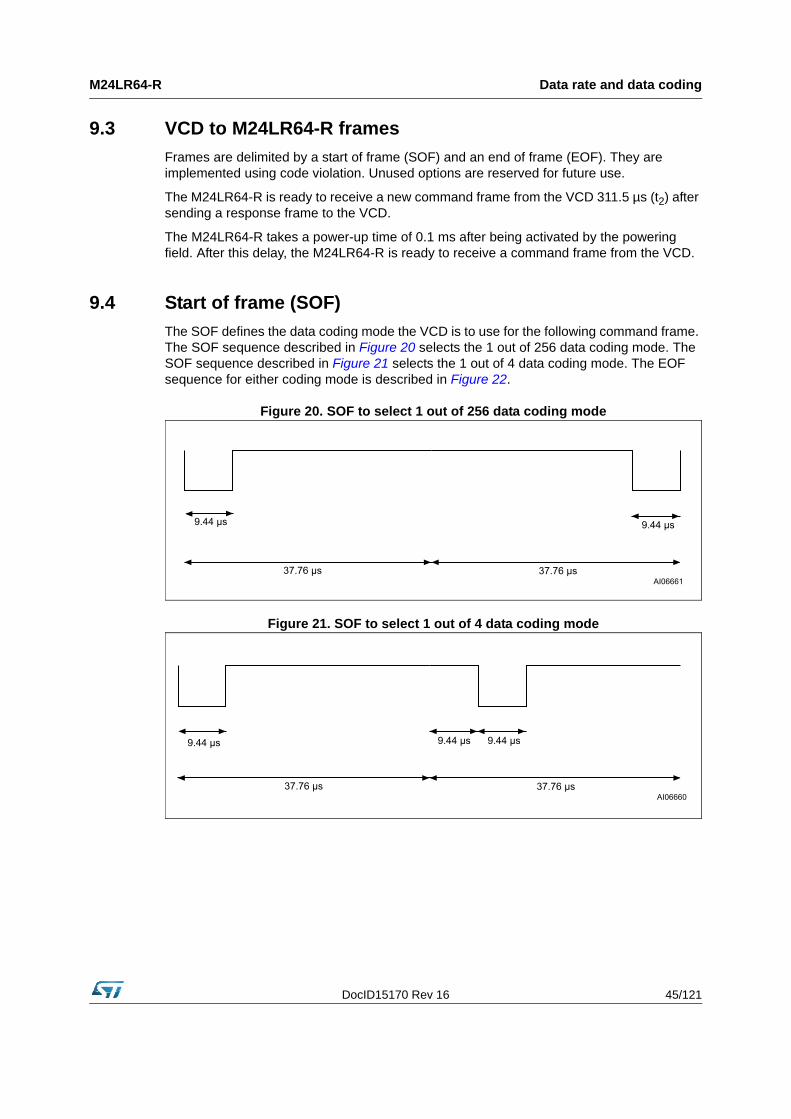
DocID15170 Rev 16 45/121
M24LR64-R Data rate and data coding
9.3 VCD to M24LR64-R frames
Frames are delimited by a start of frame (SOF) and an end of frame (EOF). They are implemented using code violation. Unused options are reserved for future use.
The M24LR64-R is ready to receive a new command frame from the VCD 311.5 µs (t2) after sending a response frame to the VCD.
The M24LR64-R takes a power-up time of 0.1 ms after being activated by the powering field. After this delay, the M24LR64-R is ready to receive a command frame from the VCD.
9.4 Start of frame (SOF)
The SOF defines the data coding mode the VCD is to use for the following command frame. The SOF sequence described in Figure 20 selects the 1 out of 256 data coding mode. The SOF sequence described in Figure 21 selects the 1 out of 4 data coding mode. The EOF sequence for either coding mode is described in Figure 22.
Figure 20. SOF to select 1 out of 256 data coding mode
Figure 21. SOF to select 1 out of 4 data coding mode

Data rate and data coding M24LR64-R
46/121 DocID15170 Rev 16
Figure 22. EOF for either data coding mode

DocID15170 Rev 16 47/121
M24LR64-R Communications signal from M24LR64-R to VCD
10 Communications signal from M24LR64-R to VCD
The M24LR64-R has several modes defined for some parameters, owing to which it can operate in different noise environments and meet different application requirements.
10.1 Load modulation
The M24LR64-R is capable of communication to the VCD via an inductive coupling area whereby the carrier is loaded to generate a subcarrier with frequency fS. The subcarrier is generated by switching a load in the M24LR64-R.
The load-modulated amplitude received on the VCD antenna must be of at least 10mV when measured as described in the test methods defined in International Standard ISO10373-7.
10.2 Subcarrier
The M24LR64-R supports the one-subcarrier and two-subcarrier response formats. These formats are selected by the VCD using the first bit in the protocol header. When one subcarrier is used, the frequency fS1 of the subcarrier load modulation is 423.75 kHz (fC/32). When two subcarriers are used, the frequency fS1 is 423.75 kHz (fC/32), and frequency fS2 is 484.28 kHz (fC/28). When using the two-subcarrier mode, the M24LR64-R generates a continuous phase relationship between fS1 and fS2.
10.3 Data rates
The M24LR64-R can respond using the low or the high data rate format. The selection of the data rate is made by the VCD using the second bit in the protocol header. It also supports the x2 mode available on all the Fast commands. Table 17 shows the different data rates produced by the M24LR64-R using the different response format combinations.
Table 17. Response data rates
Data rate One subcarrier Two subcarriers
LowStandard commands 6.62 kbit/s (fc/2048) 6.67 kbit/s (fc/2032)
Fast commands 13.24 kbit/s (fc/1024) not applicable
HighStandard commands 26.48 kbit/s (fc/512) 26.69 kbit/s (fc/508)
Fast commands 52.97 kbit/s (fc/256) not applicable

Bit representation and coding M24LR64-R
48/121 DocID15170 Rev 16
11 Bit representation and coding
Data bits are encoded using Manchester coding, according to the following schemes. For the low data rate, same subcarrier frequency or frequencies is/are used, in this case the number of pulses is multiplied by 4 and all times will increase by this factor. For the Fast commands using one subcarrier, all pulse numbers and times are divided by 2.
11.1 Bit coding using one subcarrier
11.1.1 High data rate
A logic 0 starts with 8 pulses at 423.75 kHz (fC/32) followed by an unmodulated time of 18.88 µs as shown in Figure 23.
Figure 23. Logic 0, high data rate
For the fast commands, a logic 0 starts with 4 pulses at 423.75 kHz (fC/32) followed by an unmodulated time of 9.44 µs as shown in Figure 24.
Figure 24. Logic 0, high data rate x2
A logic 1 starts with an unmodulated time of 18.88 µs followed by 8 pulses at 423.75 kHz (fC/32) as shown in Figure 25.
Figure 25. Logic 1, high data rate
For the Fast commands, a logic 1 starts with an unmodulated time of 9.44 µs followed by 4 pulses of 423.75 kHz (fC/32) as shown in Figure 26.
Figure 26. Logic 1, high data rate x2

DocID15170 Rev 16 49/121
M24LR64-R Bit representation and coding
11.1.2 Low data rate
A logic 0 starts with 32 pulses at 423.75 kHz (fC/32) followed by an unmodulated time of 75.52 µs as shown in Figure 27.
Figure 27. Logic 0, low data rate
For the Fast commands, a logic 0 starts with 16 pulses at 423.75 kHz (fC/32) followed by an unmodulated time of 37.76 µs as shown in Figure 28.
Figure 28. Logic 0, low data rate x2
A logic 1 starts with an unmodulated time of 75.52 µs followed by 32 pulses at 423.75 kHz (fC/32) as shown in Figure 29.
Figure 29. Logic 1, low data rate
For the Fast commands, a logic 1 starts with an unmodulated time of 37.76 µs followed by 16 pulses at 423.75 kHz (fC/32) as shown in Figure 29.
Figure 30. Logic 1, low data rate x2
11.2 Bit coding using two subcarriers
11.3 High data rate
A logic 0 starts with 8 pulses at 423.75 kHz (fC/32) followed by 9 pulses at 484.28 kHz (fC/28) as shown in Figure 31. For the Fast commands, the x2 mode is not available.
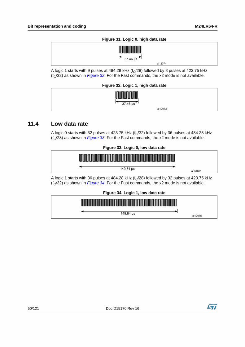
Bit representation and coding M24LR64-R
50/121 DocID15170 Rev 16
Figure 31. Logic 0, high data rate
A logic 1 starts with 9 pulses at 484.28 kHz (fC/28) followed by 8 pulses at 423.75 kHz (fC/32) as shown in Figure 32. For the Fast commands, the x2 mode is not available.
Figure 32. Logic 1, high data rate
11.4 Low data rate
A logic 0 starts with 32 pulses at 423.75 kHz (fC/32) followed by 36 pulses at 484.28 kHz (fC/28) as shown in Figure 33. For the Fast commands, the x2 mode is not available.
Figure 33. Logic 0, low data rate
A logic 1 starts with 36 pulses at 484.28 kHz (fC/28) followed by 32 pulses at 423.75 kHz (fC/32) as shown in Figure 34. For the Fast commands, the x2 mode is not available.
Figure 34. Logic 1, low data rate

DocID15170 Rev 16 51/121
M24LR64-R M24LR64-R to VCD frames
12 M24LR64-R to VCD frames
Frames are delimited by an SOF and an EOF. They are implemented using code violation. Unused options are reserved for future use. For the low data rate, the same subcarrier frequency or frequencies is/are used. In this case the number of pulses is multiplied by 4. For the Fast commands using one subcarrier, all pulse numbers and times are divided by 2.
12.1 SOF when using one subcarrier
12.2 High data rate
The SOF includes an unmodulated time of 56.64 µs, followed by 24 pulses at 423.75 kHz (fC/32), and a logic 1 that consists of an unmodulated time of 18.88 µs followed by 8 pulses at 423.75 kHz as shown in Figure 35.
Figure 35. Start of frame, high data rate, one subcarrier
For the Fast commands, the SOF comprises an unmodulated time of 28.32 µs, followed by 12 pulses at 423.75 kHz (fC/32), and a logic 1 that consists of an unmodulated time of 9.44µs followed by 4 pulses at 423.75 kHz as shown in Figure 36.
Figure 36. Start of frame, high data rate, one subcarrier x2
12.3 Low data rate
The SOF comprises an unmodulated time of 226.56 µs, followed by 96 pulses at 423.75 kHz (fC/32), and a logic 1 that consists of an unmodulated time of 75.52 µs followed by 32 pulses at 423.75 kHz as shown in Figure 37.
Figure 37. Start of frame, low data rate, one subcarrier
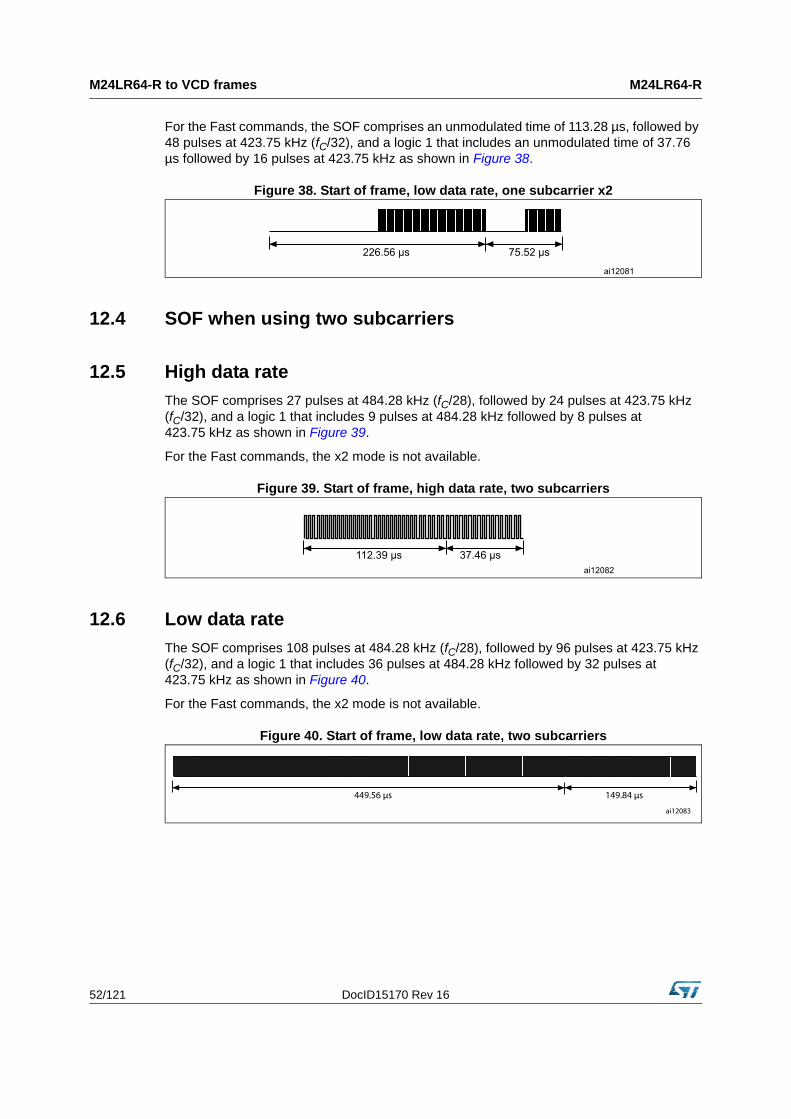
M24LR64-R to VCD frames M24LR64-R
52/121 DocID15170 Rev 16
For the Fast commands, the SOF comprises an unmodulated time of 113.28 µs, followed by 48 pulses at 423.75 kHz (fC/32), and a logic 1 that includes an unmodulated time of 37.76 µs followed by 16 pulses at 423.75 kHz as shown in Figure 38.
Figure 38. Start of frame, low data rate, one subcarrier x2
12.4 SOF when using two subcarriers
12.5 High data rate
The SOF comprises 27 pulses at 484.28 kHz (fC/28), followed by 24 pulses at 423.75 kHz (fC/32), and a logic 1 that includes 9 pulses at 484.28 kHz followed by 8 pulses at 423.75 kHz as shown in Figure 39.
For the Fast commands, the x2 mode is not available.
Figure 39. Start of frame, high data rate, two subcarriers
12.6 Low data rate
The SOF comprises 108 pulses at 484.28 kHz (fC/28), followed by 96 pulses at 423.75 kHz (fC/32), and a logic 1 that includes 36 pulses at 484.28 kHz followed by 32 pulses at 423.75 kHz as shown in Figure 40.
For the Fast commands, the x2 mode is not available.
Figure 40. Start of frame, low data rate, two subcarriers
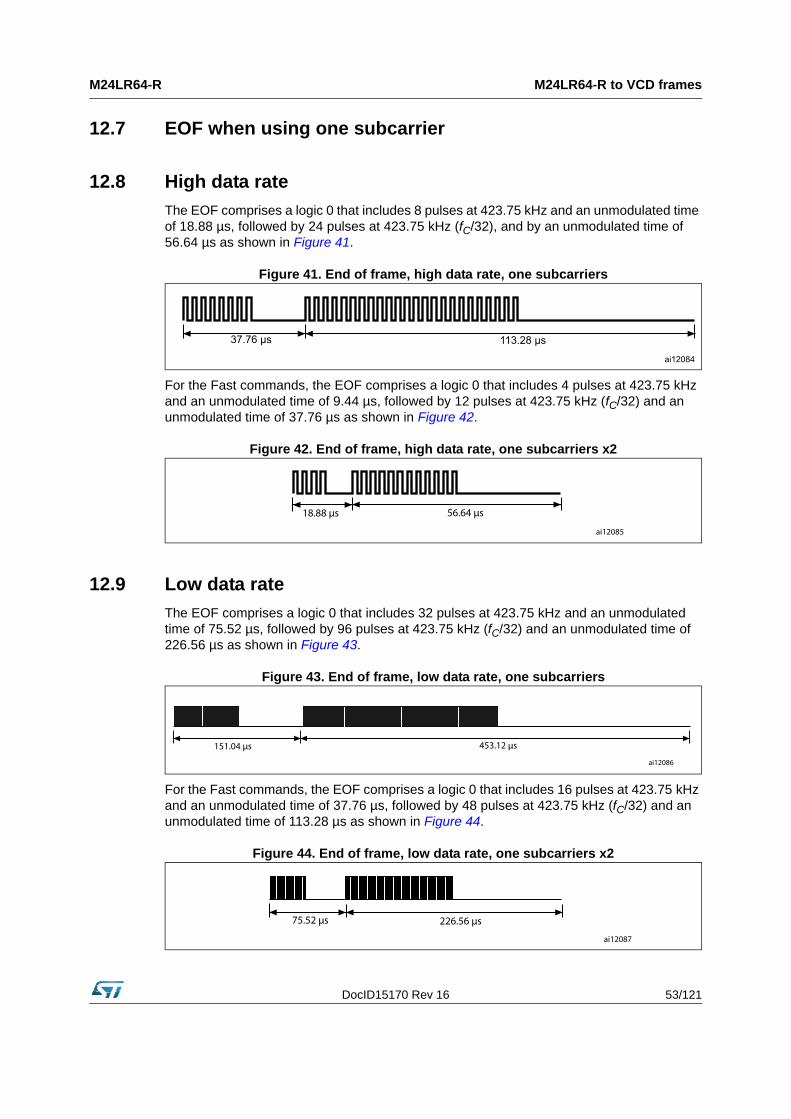
DocID15170 Rev 16 53/121
M24LR64-R M24LR64-R to VCD frames
12.7 EOF when using one subcarrier
12.8 High data rate
The EOF comprises a logic 0 that includes 8 pulses at 423.75 kHz and an unmodulated time of 18.88 µs, followed by 24 pulses at 423.75 kHz (fC/32), and by an unmodulated time of 56.64 µs as shown in Figure 41.
Figure 41. End of frame, high data rate, one subcarriers
For the Fast commands, the EOF comprises a logic 0 that includes 4 pulses at 423.75 kHz and an unmodulated time of 9.44 µs, followed by 12 pulses at 423.75 kHz (fC/32) and an unmodulated time of 37.76 µs as shown in Figure 42.
Figure 42. End of frame, high data rate, one subcarriers x2
12.9 Low data rate
The EOF comprises a logic 0 that includes 32 pulses at 423.75 kHz and an unmodulated time of 75.52 µs, followed by 96 pulses at 423.75 kHz (fC/32) and an unmodulated time of 226.56 µs as shown in Figure 43.
Figure 43. End of frame, low data rate, one subcarriers
For the Fast commands, the EOF comprises a logic 0 that includes 16 pulses at 423.75 kHz and an unmodulated time of 37.76 µs, followed by 48 pulses at 423.75 kHz (fC/32) and an unmodulated time of 113.28 µs as shown in Figure 44.
Figure 44. End of frame, low data rate, one subcarriers x2

M24LR64-R to VCD frames M24LR64-R
54/121 DocID15170 Rev 16
12.10 EOF when using two subcarriers
12.11 High data rate
The EOF comprises a logic 0 that includes 8 pulses at 423.75 kHz and 9 pulses at 484.28 kHz, followed by 24 pulses at 423.75 kHz (fC/32) and 27 pulses at 484.28 kHz (fC/28) as shown in Figure 45.
For the Fast commands, the x2 mode is not available.
Figure 45. End of frame, high data rate, two subcarriers
12.12 Low data rate
The EOF comprises a logic 0 that includes 32 pulses at 423.75 kHz and 36 pulses at 484.28 kHz, followed by 96 pulses at 423.75 kHz (fC/32) and 108 pulses at 484.28 kHz (fC/28) as shown in Figure 46.
For the Fast commands, the x2 mode is not available.
Figure 46. End of frame, low data rate, two subcarriers

DocID15170 Rev 16 55/121
M24LR64-R Unique identifier (UID)
13 Unique identifier (UID)
The M24LR64-R is uniquely identified by a 64-bit unique identifier (UID). This UID complies with ISO/IEC 15963 and ISO/IEC 7816-6. The UID is a read-only code and comprises:
• 8 MSBs with a value of E0h
• The IC manufacturer code of ST 02h, on 8 bits (ISO/IEC 7816-6/AM1)
• a unique serial number on 48 bits
With the UID each M24LR64-R can be addressed uniquely and individually during the anticollision loop and for one-to-one exchanges between a VCD and an M24LR64-R.
Table 18. UID format
MSB LSB
63 56 55 48 47 0
0xE0 0x02 Unique serial number
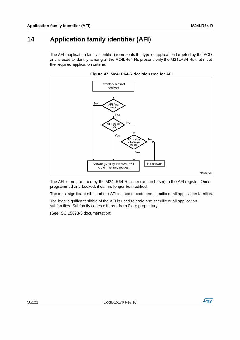
Application family identifier (AFI) M24LR64-R
56/121 DocID15170 Rev 16
14 Application family identifier (AFI)
The AFI (application family identifier) represents the type of application targeted by the VCD and is used to identify, among all the M24LR64-Rs present, only the M24LR64-Rs that meet the required application criteria.
Figure 47. M24LR64-R decision tree for AFI
The AFI is programmed by the M24LR64-R issuer (or purchaser) in the AFI register. Once programmed and Locked, it can no longer be modified.
The most significant nibble of the AFI is used to code one specific or all application families.
The least significant nibble of the AFI is used to code one specific or all application subfamilies. Subfamily codes different from 0 are proprietary.
(See ISO 15693-3 documentation)
AI15130V2
Inventory requestreceived
No
No answer
Yes
NoAFI value= 0?
Yes
No AFI flagset?
Yes
Answer given by the M24LR64to the Inventory request
AFI value= Internal
value?
DocID15170 Rev 16 57/121
M24LR64-R Data storage format identifier (DSFID)
15 Data storage format identifier (DSFID)
The data storage format identifier indicates how the data is structured in the M24LR64-R memory. The logical organization of data can be known instantly using the DSFID. It can be programmed and locked using the Write DSFID and Lock DSFID commands.
15.1 CRC
The CRC used in the M24LR64-R is calculated as per the definition in ISO/IEC 13239. The initial register contents are all ones: “FFFF”.
The two-byte CRC are appended to each request and response, within each frame, before the EOF. The CRC is calculated on all the bytes after the SOF up to the CRC field.
Upon reception of a request from the VCD, the M24LR64-R verifies that the CRC value is valid. If it is invalid, the M24LR64-R discards the frame and does not answer to the VCD.
Upon reception of a Response from the M24LR64-R, it is recommended that the VCD verifies whether the CRC value is valid. If it is invalid, actions to be performed are left to the discretion of the VCD designer.
The CRC is transmitted least significant byte first. Each byte is transmitted least significant bit first.
Table 19. CRC transmission rules
LSByte MSByte
LSBit MSBit LSBit MSBit
CRC 16 (8 bits) CRC 16 (8 bits)

M24LR64-R protocol description M24LR64-R
58/121 DocID15170 Rev 16
16 M24LR64-R protocol description
The transmission protocol (or simply protocol) defines the mechanism used to exchange instructions and data between the VCD and the M24LR64-R, in both directions. It is based on the concept of “VCD talks first”.
This means that an M24LR64-R will not start transmitting unless it has received and properly decoded an instruction sent by the VCD. The protocol is based on an exchange of:
• a request from the VCD to the M24LR64-R
• a response from the M24LR64-R to the VCD
Each request and each response are contained in a frame. The frame delimiters (SOF, EOF) are described in Section 12: M24LR64-R to VCD frames.
Each request consists of:
• a request SOF (see Figure 20 and Figure 21)
• flags
• a command code
• parameters, depending on the command
• application data
• a 2-byte CRC
• a request EOF (see Figure 22)
Each response consists of:
• an answer SOF (see Figure 35 to Figure 40)
• flags
• parameters, depending on the command
• application data
• a 2-byte CRC
• an answer EOF (see Figure 41 to Figure 46)
The protocol is bit-oriented. The number of bits transmitted in a frame is a multiple of eight (8), that is an integer number of bytes.
A single-byte field is transmitted least significant bit (LSBit) first. A multiple-byte field is transmitted least significant byte (LSByte) first, each byte is transmitted least significant bit (LSBit) first.
The setting of the flags indicates the presence of the optional fields. When the flag is set (to one), the field is present. When the flag is reset (to zero), the field is absent.
Table 20. VCD request frame format
Request SOF Request_flagsCommand
codeParameters Data 2-byte CRC
Request EOF
Table 21. M24LR64-R Response frame format
Response SOF
Response_flags Parameters Data 2-byte CRCResponse
EOF

DocID15170 Rev 16 59/121
M24LR64-R M24LR64-R protocol description
Figure 48. M24LR64-R protocol timing
VCDRequest
frame (Table 20)
Request frame
(Table 20)
M24LR64-RResponse
frame (Table 21)
Response frame
(Table 21)
Timing <-t1-> <-t2-> <-t1-> <-t2->
M24LR64-R states M24LR64-R
60/121 DocID15170 Rev 16
17 M24LR64-R states
An M24LR64-R can be in one of 4 states:
• Power-off
• Ready
• Quiet
• Selected
Transitions between these states are specified in Figure 49: M24LR64-R state transition diagram and Table 22: M24LR64-R response depending on Request_flags.
17.1 Power-off state
The M24LR64-R is in the Power-off state when it does not receive enough energy from the VCD.
17.2 Ready state
The M24LR64-R is in the Ready state when it receives enough energy from the VCD. When in the Ready state, the M24LR64-R answers any request where the Select_flag is not set.
17.3 Quiet state
When in the Quiet state, the M24LR64-R answers any request except for Inventory requests with the Address_flag set.
17.4 Selected state
In the Selected state, the M24LR64-R answers any request in all modes (see Section 18: Modes):
• Request in Select mode with the Select_flag set
• Request in Addressed mode if the UID matches
• Request in Non-Addressed mode as it is the mode for general requests

DocID15170 Rev 16 61/121
M24LR64-R M24LR64-R states
Figure 49. M24LR64-R state transition diagram
1. The M24LR64-R returns to the “Power Off” state only when both conditions are met: the VCC pin is not supplied (0 V or HiZ) and the tag is out of the RF field. Please refer to application note AN3057 for more information.
2. The intention of the state transition method is that only one M24LR64-R should be in the selected state at a time.
Table 22. M24LR64-R response depending on Request_flags
Flags
Address_flag Select_flag
1
Addressed
0
Non addressed
1
Selected
0
Non selected
M24LR64-R in Ready or Selected state (Devices in Quiet state do not answer)
X X
M24LR64-R in Selected state X X
M24LR64-R in Ready, Quiet or Selected state (the device which matches the UID)
X X
Error (03h) X X
AI06681b
Power-off
In fieldOut
of
field
Ready
QuietSelected
Any other Commandwhere Select_Flag
is not set
Stay quiet(UID)
Select (UID)
Any other commandAny other command where the
Address_Flag is set ANDwhere Inventory_Flag is not set
Stay qu
iet(U
ID) Select (UID)
Reset to ready where
Select_Flag is set or
Select(different UID)
Reset
to re
ady
Out of RF fieldafter tRF_OFF
Out of RF fieldafter tRF_OFF
after tRF_OFF
Modes M24LR64-R
62/121 DocID15170 Rev 16
18 Modes
The term “mode” refers to the mechanism used in a request to specify the set of M24LR64-Rs that will answer the request.
18.1 Addressed mode
When the Address_flag is set to 1 (Addressed mode), the request contains the Unique ID (UID) of the addressed M24LR64-R.
Any M24LR64-R that receives a request with the Address_flag set to 1 compares the received Unique ID to its own. If it matches, then the M24LR64-R executes the request (if possible) and returns a response to the VCD as specified in the command description.
If the UID does not match, then it remains silent.
18.2 Non-addressed mode (general request)
When the Address_flag is cleared to 0 (Non-Addressed mode), the request does not contain a Unique ID. Any M24LR64-R receiving a request with the Address_flag cleared to 0 executes it and returns a response to the VCD as specified in the command description.
18.3 Select mode
When the Select_flag is set to 1 (Select mode), the request does not contain an M24LR64-R Unique ID. The M24LR64-R in the Selected state that receives a request with the Select_flag set to 1 executes it and returns a response to the VCD as specified in the command description.
Only M24LR64-Rs in the Selected state answer a request where the Select_flag set to 1.
The system design ensures in theory that only one M24LR64-R can be in the Select state at a time.
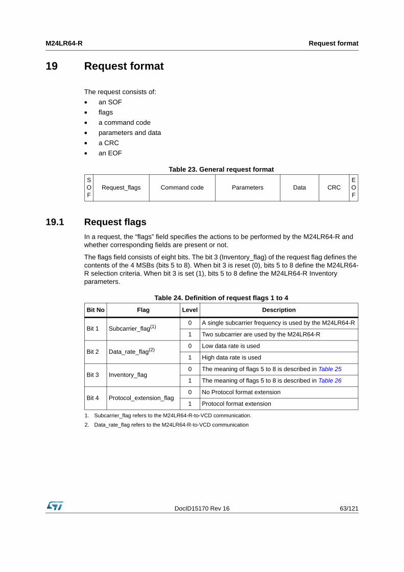
DocID15170 Rev 16 63/121
M24LR64-R Request format
19 Request format
The request consists of:
• an SOF
• flags
• a command code
• parameters and data
• a CRC
• an EOF
19.1 Request flags
In a request, the “flags” field specifies the actions to be performed by the M24LR64-R and whether corresponding fields are present or not.
The flags field consists of eight bits. The bit 3 (Inventory_flag) of the request flag defines the contents of the 4 MSBs (bits 5 to 8). When bit 3 is reset (0), bits 5 to 8 define the M24LR64-R selection criteria. When bit 3 is set (1), bits 5 to 8 define the M24LR64-R Inventory parameters.
Table 23. General request format
SOF
Request_flags Command code Parameters Data CRCEOF
Table 24. Definition of request flags 1 to 4
Bit No Flag Level Description
Bit 1 Subcarrier_flag(1)
1. Subcarrier_flag refers to the M24LR64-R-to-VCD communication.
0 A single subcarrier frequency is used by the M24LR64-R
1 Two subcarrier are used by the M24LR64-R
Bit 2 Data_rate_flag(2)
2. Data_rate_flag refers to the M24LR64-R-to-VCD communication
0 Low data rate is used
1 High data rate is used
Bit 3 Inventory_flag0 The meaning of flags 5 to 8 is described in Table 25
1 The meaning of flags 5 to 8 is described in Table 26
Bit 4 Protocol_extension_flag0 No Protocol format extension
1 Protocol format extension

Request format M24LR64-R
64/121 DocID15170 Rev 16
.
Table 25. Request flags 5 to 8 when Bit 3 = 0
Bit No Flag Level Description
Bit 5 Select flag(1)
1. If the Select_flag is set to 1, the Address_flag is set to 0 and the UID field is not present in the request.
0Request is executed by any M24LR64-R according to the setting of Address_flag
1 Request is executed only by the M24LR64-R in Selected state
Bit 6Address flag(1)
0Request is not addressed. UID field is not present. The request is executed by all M24LR64-Rs.
1Request is addressed. UID field is present. The request is executed only by the M24LR64-R whose UID matches the UID specified in the request.
Bit 7 Option flag0 Option not activated.
1 Option activated.
Bit 8 RFU 0 -
Table 26. Request flags 5 to 8 when Bit 3 = 1
Bit No Flag Level Description
Bit 5 AFI flag0 AFI field is not present
1 AFI field is present
Bit 6 Nb_slots flag0 16 slots
1 1 slot
Bit 7 Option flag 0 -
Bit 8 RFU 0 -

DocID15170 Rev 16 65/121
M24LR64-R Response format
20 Response format
The response consists of:
• an SOF
• flags
• parameters and data
• a CRC
• an EOF
20.1 Response flags
In a response, the flags indicate how actions have been performed by the M24LR64-R and whether corresponding fields are present or not. The response flags consist of eight bits.
Table 27. General response format
SOF
Response_flags Parameters Data CRCEOF
Table 28. Definitions of response flags 1 to 8
Bit No Flag Level Description
Bit 1 Error_flag0 No error
1 Error detected. Error code is in the “Error” field.
Bit 2 RFU 0 -
Bit 3 RFU 0 -
Bit 4 Extension flag 0 No extension
Bit 5 RFU 0 -
Bit 6 RFU 0 -
Bit 7 RFU 0 -
Bit 8 RFU 0 -
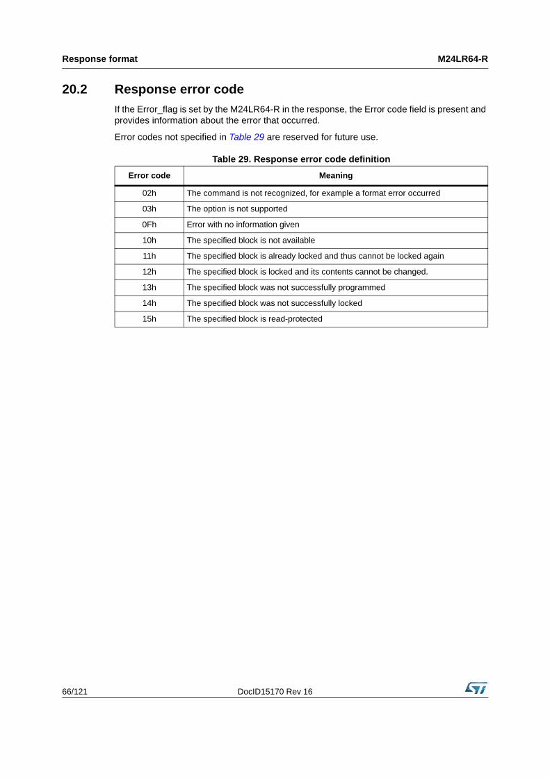
Response format M24LR64-R
66/121 DocID15170 Rev 16
20.2 Response error code
If the Error_flag is set by the M24LR64-R in the response, the Error code field is present and provides information about the error that occurred.
Error codes not specified in Table 29 are reserved for future use.
Table 29. Response error code definition
Error code Meaning
02h The command is not recognized, for example a format error occurred
03h The option is not supported
0Fh Error with no information given
10h The specified block is not available
11h The specified block is already locked and thus cannot be locked again
12h The specified block is locked and its contents cannot be changed.
13h The specified block was not successfully programmed
14h The specified block was not successfully locked
15h The specified block is read-protected
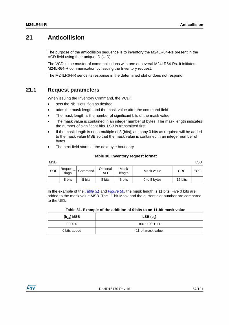
DocID15170 Rev 16 67/121
M24LR64-R Anticollision
21 Anticollision
The purpose of the anticollision sequence is to inventory the M24LR64-Rs present in the VCD field using their unique ID (UID).
The VCD is the master of communications with one or several M24LR64-Rs. It initiates M24LR64-R communication by issuing the Inventory request.
The M24LR64-R sends its response in the determined slot or does not respond.
21.1 Request parameters
When issuing the Inventory Command, the VCD:
• sets the Nb_slots_flag as desired
• adds the mask length and the mask value after the command field
• The mask length is the number of significant bits of the mask value.
• The mask value is contained in an integer number of bytes. The mask length indicates the number of significant bits. LSB is transmitted first
• If the mask length is not a multiple of 8 (bits), as many 0 bits as required will be added to the mask value MSB so that the mask value is contained in an integer number of bytes
• The next field starts at the next byte boundary.
In the example of the Table 31 and Figure 50, the mask length is 11 bits. Five 0 bits are added to the mask value MSB. The 11-bit Mask and the current slot number are compared to the UID.
Table 30. Inventory request format
MSB LSB
SOFRequest_
flagsCommand
Optional AFI
Mask length
Mask value CRC EOF
8 bits 8 bits 8 bits 8 bits 0 to 8 bytes 16 bits
Table 31. Example of the addition of 0 bits to an 11-bit mask value
(b15) MSB LSB (b0)
0000 0 100 1100 1111
0 bits added 11-bit mask value

Anticollision M24LR64-R
68/121 DocID15170 Rev 16
Figure 50. Principle of comparison between the mask, the slot number and the UID
The AFI field is present if the AFI_flag is set.
The pulse is generated according to the definition of the EOF in ISO/IEC 15693-2.
The first slot starts immediately after the reception of the request EOF. To switch to the next slot, the VCD sends an EOF.
The following rules and restrictions apply:
• if no M24LR64-R answer is detected, the VCD may switch to the next slot by sending an EOF,
• if one or more M24LR64-R answers are detected, the VCD waits until the complete frame has been received before sending an EOF for switching to the next slot.
AI06682
Mask value received in the Inventory command 0000 0100 1100 1111b 16 bits
The Mask value less the padding 0s is loadedinto the Tag comparator
100 1100 1111 b 11 bits
The Slot counter is calculatedxxxxNb_slots_flags = 0 (16 slots), Slot Counter is 4 bits
The Slot counter is concatened to the Mask valuexxxx 100 1100 1111 bNb_slots_flags = 0 15 bits
The concatenated result is compared withthe least significant bits of the Tag UID.
xxxx xxxx ..... xxxx xxxx x xxx xxxx xxxx xxxx 64 bits
LSBMSB
b
LSBMSB
LSBMSB
LSBMSB
b0b63
CompareBits ignored
UID
4 bits
DocID15170 Rev 16 69/121
M24LR64-R Request processing by the M24LR64-R
22 Request processing by the M24LR64-R
Upon reception of a valid request, the M24LR64-R performs the following algorithm:
• NbS is the total number of slots (1 or 16)
• SN is the current slot number (0 to 15)
• LSB (value, n) function returns the n Less Significant Bits of value
• MSB (value, n) function returns the n Most Significant Bits of value
• “&” is the concatenation operator
• Slot_Frame is either an SOF or an EOF
SN = 0if (Nb_slots_flag)
then NbS = 1SN_length = 0endif
else NbS = 16SN_length = 4endif
label1:if LSB(UID, SN_length + Mask_length) =
LSB(SN,SN_length)&LSB(Mask,Mask_length) then answer to inventory request
endif
wait (Slot_Frame)
if Slot_Frame = SOF then Stop Anticollision
decode/process requestexitendif
if Slot_Frame = EOFif SN < NbS-1
then SN = SN + 1goto label1exitendif
endif
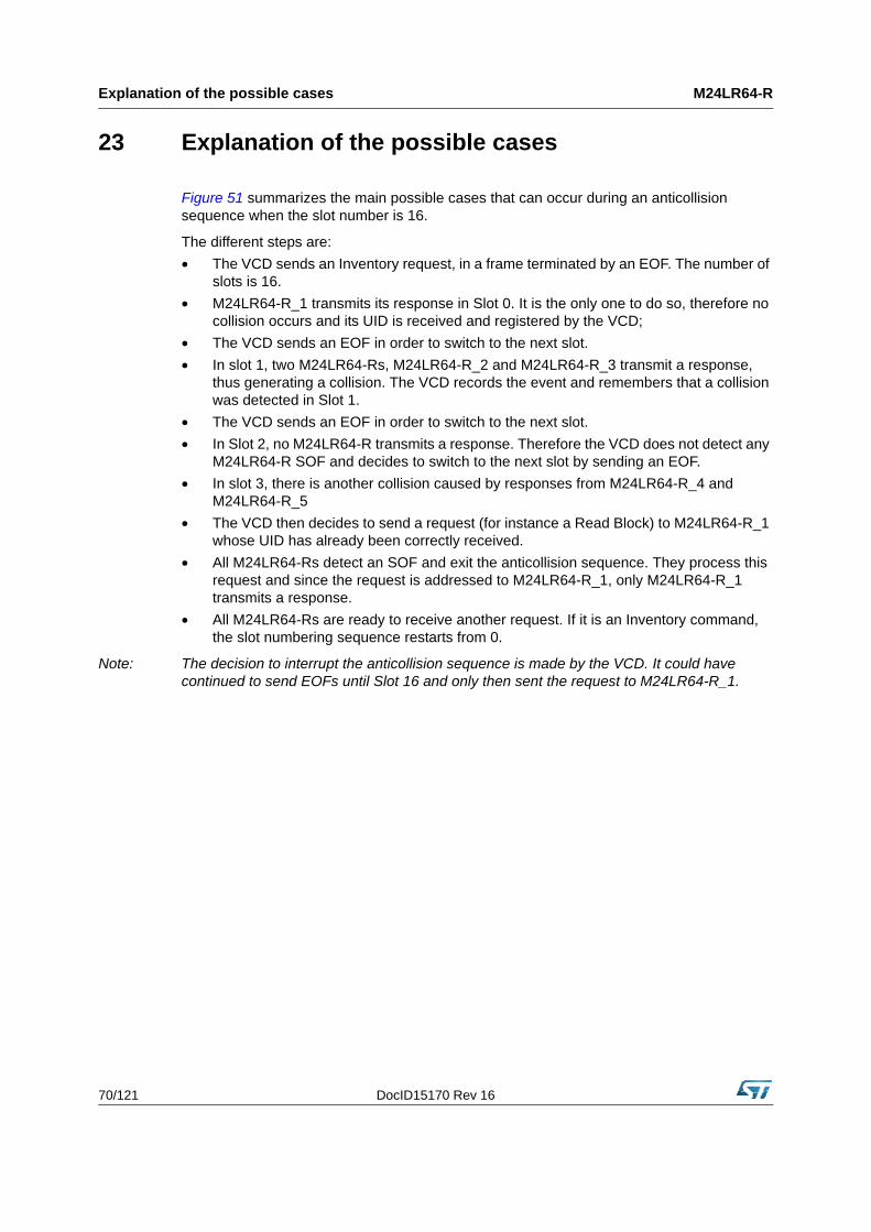
Explanation of the possible cases M24LR64-R
70/121 DocID15170 Rev 16
23 Explanation of the possible cases
Figure 51 summarizes the main possible cases that can occur during an anticollision sequence when the slot number is 16.
The different steps are:
• The VCD sends an Inventory request, in a frame terminated by an EOF. The number of slots is 16.
• M24LR64-R_1 transmits its response in Slot 0. It is the only one to do so, therefore no collision occurs and its UID is received and registered by the VCD;
• The VCD sends an EOF in order to switch to the next slot.
• In slot 1, two M24LR64-Rs, M24LR64-R_2 and M24LR64-R_3 transmit a response, thus generating a collision. The VCD records the event and remembers that a collision was detected in Slot 1.
• The VCD sends an EOF in order to switch to the next slot.
• In Slot 2, no M24LR64-R transmits a response. Therefore the VCD does not detect any M24LR64-R SOF and decides to switch to the next slot by sending an EOF.
• In slot 3, there is another collision caused by responses from M24LR64-R_4 and M24LR64-R_5
• The VCD then decides to send a request (for instance a Read Block) to M24LR64-R_1 whose UID has already been correctly received.
• All M24LR64-Rs detect an SOF and exit the anticollision sequence. They process this request and since the request is addressed to M24LR64-R_1, only M24LR64-R_1 transmits a response.
• All M24LR64-Rs are ready to receive another request. If it is an Inventory command, the slot numbering sequence restarts from 0.
Note: The decision to interrupt the anticollision sequence is made by the VCD. It could have continued to send EOFs until Slot 16 and only then sent the request to M24LR64-R_1.
DocID15170 Rev 16 71/121
M24LR64-R Explanation of the possible cases
Figure 51. Description of a possible anticollision sequence
AI1
5117
V2
Slo
t 0S
lot 1
Slo
t 2S
lot 3
VC
DS
OF
Inve
ntor
y R
eque
stE
OF
EO
FE
OF
EO
FS
OF
Req
uest
to
M24
LR64
_1E
OF
Res
pons
e 2
Res
pons
e 4
M24
LR64
sR
espo
nse
from
M
24LR
64_1
Res
pons
e 1
Res
pons
e 3
Res
pons
e 5
Tim
ing
t1t2
t1t2
t3t1
t2t1
Com
men
tN
o co
llisi
onC
ollis
ion
No
Res
pons
eC
ollis
ion
Tim
e
Inventory Initiated command M24LR64-R
72/121 DocID15170 Rev 16
24 Inventory Initiated command
The M24LR64-R provides a special feature to improve the inventory time response of moving tags using the Initiate_flag value. This flag, controlled by the Initiate command, allows tags to answer to Inventory Initiated commands.
For applications in which multiple tags are moving in front of a reader, it is possible to miss tags using the standard inventory command. The reason is that the inventory sequence has to be performed on a global tree search. For example, a tag with a particular UID value may have to wait the run of a long tree search before being inventoried. If the delay is too long, the tag may be out of the field before it has been detected.
Using the Initiate command, the inventory sequence is optimized. When multiple tags are moving in front of a reader, the ones which are within the reader field will be initiated by the Initiate command. In this case, a small batch of tags will answer to the Inventory Initiated command which will optimize the time necessary to identify all the tags. When finished, the reader has to issue a new Initiate command in order to initiate a new small batch of tags which are new inside the reader field.
It is also possible to reduce the inventory sequence time using the Fast Initiate and Fast Inventory Initiated commands. These commands allow the M24LR64-Rs to increase their response data rate by a factor of 2, up to 53 kbit/s.
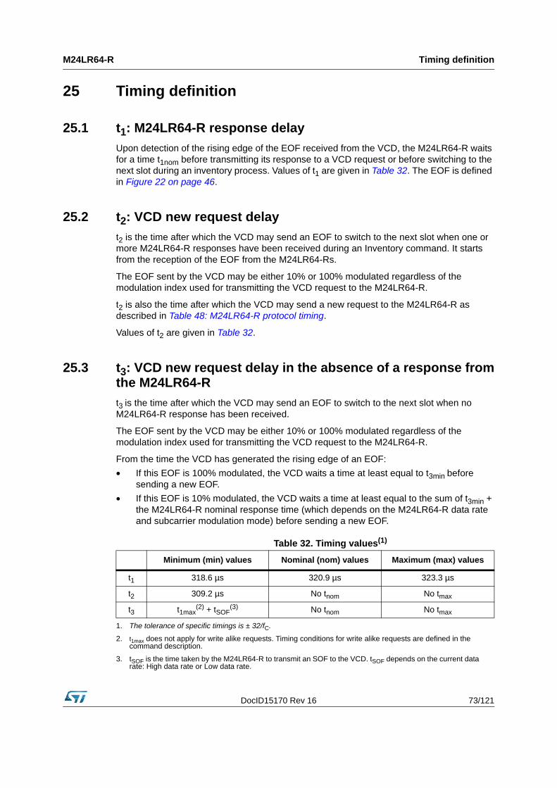
DocID15170 Rev 16 73/121
M24LR64-R Timing definition
25 Timing definition
25.1 t1: M24LR64-R response delay
Upon detection of the rising edge of the EOF received from the VCD, the M24LR64-R waits for a time t1nom before transmitting its response to a VCD request or before switching to the next slot during an inventory process. Values of t1 are given in Table 32. The EOF is defined in Figure 22 on page 46.
25.2 t2: VCD new request delay
t2 is the time after which the VCD may send an EOF to switch to the next slot when one or more M24LR64-R responses have been received during an Inventory command. It starts from the reception of the EOF from the M24LR64-Rs.
The EOF sent by the VCD may be either 10% or 100% modulated regardless of the modulation index used for transmitting the VCD request to the M24LR64-R.
t2 is also the time after which the VCD may send a new request to the M24LR64-R as described in Table 48: M24LR64-R protocol timing.
Values of t2 are given in Table 32.
25.3 t3: VCD new request delay in the absence of a response fromthe M24LR64-R
t3 is the time after which the VCD may send an EOF to switch to the next slot when no M24LR64-R response has been received.
The EOF sent by the VCD may be either 10% or 100% modulated regardless of the modulation index used for transmitting the VCD request to the M24LR64-R.
From the time the VCD has generated the rising edge of an EOF:
• If this EOF is 100% modulated, the VCD waits a time at least equal to t3min before sending a new EOF.
• If this EOF is 10% modulated, the VCD waits a time at least equal to the sum of t3min + the M24LR64-R nominal response time (which depends on the M24LR64-R data rate and subcarrier modulation mode) before sending a new EOF.
Table 32. Timing values(1)
1. The tolerance of specific timings is ± 32/fC.
Minimum (min) values Nominal (nom) values Maximum (max) values
t1 318.6 µs 320.9 µs 323.3 µs
t2 309.2 µs No tnom No tmax
t3 t1max(2) + tSOF
(3)
2. t1max does not apply for write alike requests. Timing conditions for write alike requests are defined in the command description.
3. tSOF is the time taken by the M24LR64-R to transmit an SOF to the VCD. tSOF depends on the current data rate: High data rate or Low data rate.
No tnom No tmax
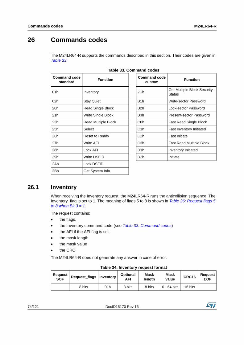
Commands codes M24LR64-R
74/121 DocID15170 Rev 16
26 Commands codes
The M24LR64-R supports the commands described in this section. Their codes are given in Table 33.
26.1 Inventory
When receiving the Inventory request, the M24LR64-R runs the anticollision sequence. The Inventory_flag is set to 1. The meaning of flags 5 to 8 is shown in Table 26: Request flags 5 to 8 when Bit 3 = 1.
The request contains:
• the flags,
• the Inventory command code (see Table 33: Command codes)
• the AFI if the AFI flag is set
• the mask length
• the mask value
• the CRC
The M24LR64-R does not generate any answer in case of error.
Table 33. Command codes
Command codestandard
FunctionCommand code
customFunction
01h Inventory 2ChGet Multiple Block Security Status
02h Stay Quiet B1h Write-sector Password
20h Read Single Block B2h Lock-sector Password
21h Write Single Block B3h Present-sector Password
23h Read Multiple Block C0h Fast Read Single Block
25h Select C1h Fast Inventory Initiated
26h Reset to Ready C2h Fast Initiate
27h Write AFI C3h Fast Read Multiple Block
28h Lock AFI D1h Inventory Initiated
29h Write DSFID D2h Initiate
2Ah Lock DSFID
2Bh Get System Info
Table 34. Inventory request format
Request SOF
Request_flags InventoryOptional
AFIMask length
Mask value
CRC16Request
EOF
8 bits 01h 8 bits 8 bits 0 - 64 bits 16 bits

DocID15170 Rev 16 75/121
M24LR64-R Commands codes
The response contains:
• the flags
• the Unique ID
During an Inventory process, if the VCD does not receive an RF M24LR64-R response, it waits a time t3 before sending an EOF to switch to the next slot. t3 starts from the rising edge of the request EOF sent by the VCD.
• If the VCD sends a 100% modulated EOF, the minimum value of t3 is:t3min = 4384/fC (323.3 µs) + tSOF
• If the VCD sends a 10% modulated EOF, the minimum value of t3 is:t3min = 4384/fC (323.3 µs) + tNRT
where:
• tSOF is the time required by the M24LR64-R to transmit an SOF to the VCD
• tNRT is the nominal response time of the M24LR64-R
tNRT and tSOF are dependent on the M24LR64-R-to-VCD data rate and subcarrier modulation mode.
26.2 Stay Quiet
Command code = 0x02
On receiving the Stay Quiet command, the M24LR64-R enters the Quiet State if no error occurs, and does NOT send back a response. There is NO response to the Stay Quiet command even if an error occurs.
When in the Quiet state:
• the M24LR64-R does not process any request if the Inventory_flag is set,
• the M24LR64-R processes any Addressed request
The M24LR64-R exits the Quiet State when:
• it is reset (power off),
• receiving a Select request. It then goes to the Selected state,
• receiving a Reset to Ready request. It then goes to the Ready state.
The Stay Quiet command must always be executed in Addressed mode (Select_flag is reset to 0 and Address_flag is set to 1).
Table 35. Inventory response format
Response SOF
Response_flags
DSFID UID CRC16Response
EOF
8 bits 8 bits 64 bits 16 bits
Table 36. Stay Quiet request format
Request SOF
Request flags Stay Quiet UID CRC16Request
EOF
8 bits 02h 64 bits 16 bits

Commands codes M24LR64-R
76/121 DocID15170 Rev 16
26.3 Read Single Block
On receiving the Read Single Block command, the M24LR64-R reads the requested block and sends back its 32-bit value in the response. The Protocol_extention_flag should be set to 1 for the M24LR64-R to operate correctly. If the Protocol_extention_flag is at 0, the M24LR64-R answers with an error code. The Option_flag is supported.
Request parameters:
• Option_flag
• UID (optional)
• Block number
Response parameters:
• Sector security status if Option_flag is set (see Table 39: Sector security status)
• 4 bytes of block data
Figure 52. Stay Quiet frame exchange between VCD and M24LR64-R
VCD SOFStay Quiet
requestEOF
M24LR64-R
Timing
Table 37. Read Single Block request format
Request SOF
Request_flags
Read Single Block
UID(1)
1. Gray means that the field is optional.
Block number
CRC16Request
EOF
8 bits 20h 64 bits 16 bits 16 bits
Table 38. Read Single Block response format when Error_flag is NOT set
Response SOF
Response_flagsSector
security status(1)
1. Gray means that the field is optional.
Data CRC16Response
EOF
8 bits 8 bits 32 bits 16 bits
Table 39. Sector security status
b7 b6 b5 b4 b3 b2 b1 b0
Reserved for future use. All at 0
password control bits
Read / Write protection bits
0: Current sector not locked
1: Current sector locked

DocID15170 Rev 16 77/121
M24LR64-R Commands codes
Response parameter:
• Error code as Error_flag is set
– 03h: the option is not supported
– 0Fh: error with no information given
– 10h: the specified block is not available
– 15h: the specified block is read-protected
26.4 Write Single Block
On receiving the Write Single Block command, the M24LR64-R writes the data contained in the request to the requested block and reports whether the write operation was successful in the response. The Protocol_extention_flag should be set to 1 for the M24LR64-R to operate correctly. If the Protocol_extention_flag is at 0, the M24LR64-R answers with an error code. The Option_flag is supported.
During the RF write cycle Wt, there should be no modulation (neither 100% nor 10%). Otherwise, the M24LR64-R may not program correctly the data into the memory. The Wt time is equal to t1nom + 18 × 302 µs.
Request parameters:
• UID (optional)
• Block number
• Data
Table 40. Read Single Block response format when Error_flag is set
Response SOF
Response_flags
Error code CRC16Response
EOF
8 bits 8 bits 16 bits
Figure 53. Read Single Block frame exchange between VCD and M24LR64-R
VCD SOFRead Single Block
requestEOF
M24LR64-R <-t1-> SOFRead Single Block
responseEOF
Table 41. Write Single Block request format
Request SOF
Request_flags
Write Single Block
UID(1)
1. Gray means that the field is optional.
Block number
Data CRC16Request
EOF
8 bits 21h 64 bits 16 bits 32 bits 16 bits

Commands codes M24LR64-R
78/121 DocID15170 Rev 16
Response parameter:
• No parameter. The response is send back after the writing cycle.
Response parameter:
• Error code as Error_flag is set:
– 03h: the option is not supported
– 0Fh: error with no information given
– 10h: the specified block is not available
– 12h: the specified block is locked and its contents cannot be changed.
– 13h: the specified block was not successfully programmed
26.5 Read Multiple Block
When receiving the Read Multiple Block command, the M24LR64-R reads the selected blocks and sends back their value in multiples of 32 bits in the response. The blocks are numbered from '00h to '7FFh' in the request and the value is minus one (–1) in the field. For example, if the “number of blocks” field contains the value 06h, 7 blocks are read. The maximum number of blocks is fixed at 32 assuming that they are all located in the same sector. If the number of blocks overlaps sectors, the M24LR64-R returns an error code.The Protocol_extention_flag should be set to 1 for the M24LR64-R to operate correctly. If the Protocol_extention_flag is at 0, the M24LR64-R answers with an error code.The Option_flag is supported.
Table 42. Write Single Block response format when Error_flag is NOT set
Response SOF Response_flags CRC16 Response EOF
8 bits 16 bits
Table 43. Write Single Block response format when Error_flag is set
Response SOF
Response_flags
Error code CRC16Response
EOF
8 bits 8 bits 16 bits
Figure 54. Write Single Block frame exchange between VCD and M24LR64-R
VCD SOFWrite Single
Block requestEOF
M24LR64-R <-t1-> SOFWrite Single
Block responseEOF
Write sequence when error
M24LR64-R <------------------- Wt ---------------> SOFWrite Single
Block responseEOF

DocID15170 Rev 16 79/121
M24LR64-R Commands codes
Request parameters:
• Option_flag
• UID (optional)
• First block number
• Number of blocks
Response parameters:
• Sector security status if Option_flag is set (see Table 46: Sector security status)
• N blocks of data
Response parameter:
• Error code as Error_flag is set:
– 03h: the option is not supported
– 0Fh: error with no information given
– 10h: the specified block is not available
– 15h: the specified block is read-protected
Table 44. Read Multiple Block request format
Request SOF
Request_flags
Read Multiple Block
UID(1)
1. Gray means that the field is optional.
First block
number
Number of blocks
CRC16Request
EOF
8 bits 23h 64 bits 16 bits 8 bits 16 bits
Table 45. Read Multiple Block response format when Error_flag is NOT set
Response SOF
Response_flags
Sector security status(1)
1. Gray means that the field is optional.
Data CRC16Response
EOF
8 bits 8 bits(2)
2. Repeated as needed.
32 bits(2) 16 bits
Table 46. Sector security status
b7 b6 b5 b4 b3 b2 b1 b0
Reserved for future use. All at 0
password control bits
Read / Write protection bits
0: Current sector not locked1: Current sector locked
Table 47. Read Multiple Block response format when Error_flag is set
Response SOF Response_flags Error code CRC16 Response EOF
8 bits 8 bits 16 bits
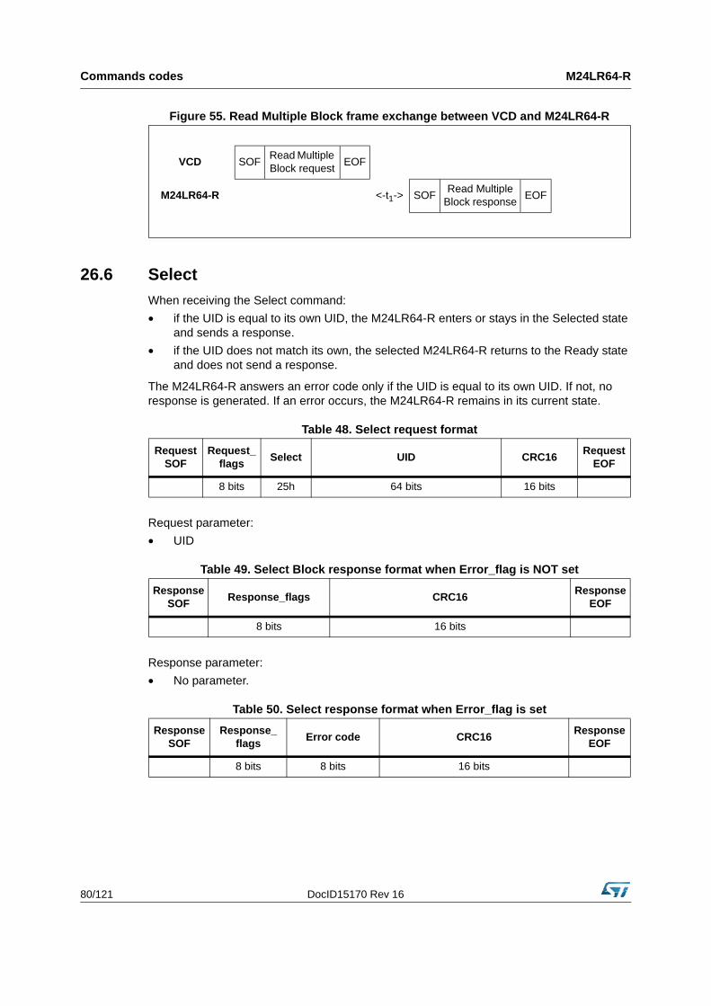
Commands codes M24LR64-R
80/121 DocID15170 Rev 16
26.6 Select
When receiving the Select command:
• if the UID is equal to its own UID, the M24LR64-R enters or stays in the Selected state and sends a response.
• if the UID does not match its own, the selected M24LR64-R returns to the Ready state and does not send a response.
The M24LR64-R answers an error code only if the UID is equal to its own UID. If not, no response is generated. If an error occurs, the M24LR64-R remains in its current state.
Request parameter:
• UID
Response parameter:
• No parameter.
Figure 55. Read Multiple Block frame exchange between VCD and M24LR64-R
VCD SOFRead Multiple Block request
EOF
M24LR64-R <-t1-> SOFRead Multiple
Block responseEOF
Table 48. Select request format
Request SOF
Request_flags
Select UID CRC16Request
EOF
8 bits 25h 64 bits 16 bits
Table 49. Select Block response format when Error_flag is NOT set
Response SOF
Response_flags CRC16Response
EOF
8 bits 16 bits
Table 50. Select response format when Error_flag is set
Response SOF
Response_flags
Error code CRC16Response
EOF
8 bits 8 bits 16 bits
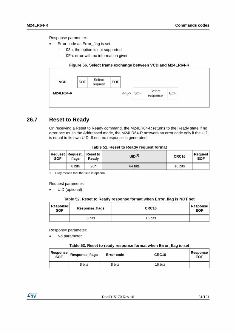
DocID15170 Rev 16 81/121
M24LR64-R Commands codes
Response parameter:
• Error code as Error_flag is set:
– 03h: the option is not supported
– 0Fh: error with no information given
26.7 Reset to Ready
On receiving a Reset to Ready command, the M24LR64-R returns to the Ready state if no error occurs. In the Addressed mode, the M24LR64-R answers an error code only if the UID is equal to its own UID. If not, no response is generated.
Request parameter:
• UID (optional)
Response parameter:
• No parameter
Figure 56. Select frame exchange between VCD and M24LR64-R
VCD SOFSelect
requestEOF
M24LR64-R <-t1-> SOFSelect
responseEOF
Table 51. Reset to Ready request format
Request SOF
Request_flags
Reset to Ready
UID(1)
1. Gray means that the field is optional.
CRC16Request
EOF
8 bits 26h 64 bits 16 bits
Table 52. Reset to Ready response format when Error_flag is NOT set
Response SOF
Response_flags CRC16Response
EOF
8 bits 16 bits
Table 53. Reset to ready response format when Error_flag is set
Response SOF
Response_flags Error code CRC16Response
EOF
8 bits 8 bits 16 bits
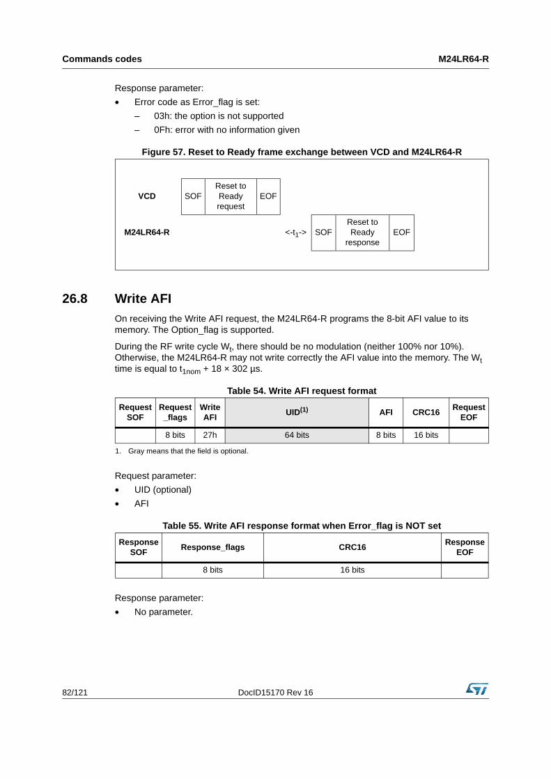
Commands codes M24LR64-R
82/121 DocID15170 Rev 16
Response parameter:
• Error code as Error_flag is set:
– 03h: the option is not supported
– 0Fh: error with no information given
26.8 Write AFI
On receiving the Write AFI request, the M24LR64-R programs the 8-bit AFI value to its memory. The Option_flag is supported.
During the RF write cycle Wt, there should be no modulation (neither 100% nor 10%). Otherwise, the M24LR64-R may not write correctly the AFI value into the memory. The Wt time is equal to t1nom + 18 × 302 µs.
Request parameter:
• UID (optional)
• AFI
Response parameter:
• No parameter.
Figure 57. Reset to Ready frame exchange between VCD and M24LR64-R
VCD SOFReset to Ready request
EOF
M24LR64-R <-t1-> SOFReset to Ready
responseEOF
Table 54. Write AFI request format
Request SOF
Request_flags
Write AFI
UID(1)
1. Gray means that the field is optional.
AFI CRC16Request
EOF
8 bits 27h 64 bits 8 bits 16 bits
Table 55. Write AFI response format when Error_flag is NOT set
Response SOF
Response_flags CRC16Response
EOF
8 bits 16 bits
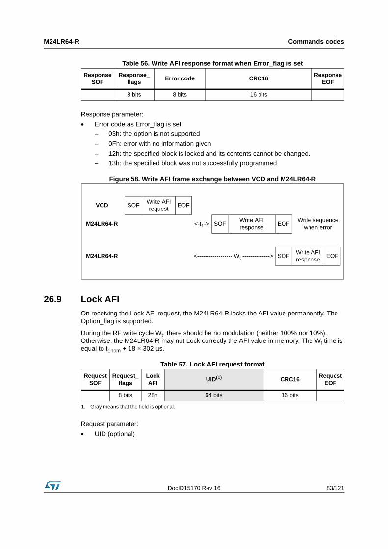
DocID15170 Rev 16 83/121
M24LR64-R Commands codes
Response parameter:
• Error code as Error_flag is set
– 03h: the option is not supported
– 0Fh: error with no information given
– 12h: the specified block is locked and its contents cannot be changed.
– 13h: the specified block was not successfully programmed
26.9 Lock AFI
On receiving the Lock AFI request, the M24LR64-R locks the AFI value permanently. The Option_flag is supported.
During the RF write cycle Wt, there should be no modulation (neither 100% nor 10%). Otherwise, the M24LR64-R may not Lock correctly the AFI value in memory. The Wt time is equal to t1nom + 18 × 302 µs.
Request parameter:
• UID (optional)
Table 56. Write AFI response format when Error_flag is set
Response SOF
Response_flags
Error code CRC16Response
EOF
8 bits 8 bits 16 bits
Figure 58. Write AFI frame exchange between VCD and M24LR64-R
VCD SOFWrite AFI request
EOF
M24LR64-R <-t1-> SOFWrite AFI response
EOFWrite sequence
when error
M24LR64-R <------------------ Wt --------------> SOFWrite AFI response
EOF
Table 57. Lock AFI request format
Request SOF
Request_flags
Lock AFI
UID(1)
1. Gray means that the field is optional.
CRC16Request
EOF
8 bits 28h 64 bits 16 bits
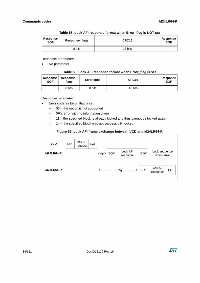
Commands codes M24LR64-R
84/121 DocID15170 Rev 16
Response parameter:
• No parameter
Response parameter:
• Error code as Error_flag is set
– 03h: the option is not supported
– 0Fh: error with no information given
– 11h: the specified block is already locked and thus cannot be locked again
– 14h: the specified block was not successfully locked
Table 58. Lock AFI response format when Error_flag is NOT set
Response SOF
Response_flags CRC16Response
EOF
8 bits 16 bits
Table 59. Lock AFI response format when Error_flag is set
Response SOF
Response_flags
Error code CRC16Response
EOF
8 bits 8 bits 16 bits
Figure 59. Lock AFI frame exchange between VCD and M24LR64-R
VCD SOFLock AFI request
EOF
M24LR64-R <-t1-> SOFLock AFI response
EOFLock sequence
when error
M24LR64-R <----------------- Wt -------------> SOFLock AFI response
EOF
DocID15170 Rev 16 85/121
M24LR64-R Commands codes
26.10 Write DSFID
On receiving the Write DSFID request, the M24LR64-R programs the 8-bit DSFID value to its memory. The Option_flag is supported.
During the RF write cycle Wt, there should be no modulation (neither 100% nor 10%). Otherwise, the M24LR64-R may not write correctly the DSFID value in memory. The Wt time is equal to t1nom + 18 × 302 µs.
Request parameter:
• UID (optional)
• DSFID
Response parameter:
• No parameter
Response parameter:
• Error code as Error_flag is set
– 03h: the option is not supported
– 0Fh: error with no information given
– 12h: the specified block is locked and its contents cannot be changed.
– 13h: the specified block was not successfully programmed
Table 60. Write DSFID request format
Request SOF
Request_flags
Write DSFID
UID(1)
1. Gray means that the field is optional.
DSFID CRC16Request
EOF
8 bits 29h 64 bits 8 bits 16 bits
Table 61. Write DSFID response format when Error_flag is NOT set
Response SOF
Response_flags CRC16Response
EOF
8 bits 16 bits
Table 62. Write DSFID response format when Error_flag is set
Response SOF
Response_flags Error code CRC16Response
EOF
8 bits 8 bits 16 bits
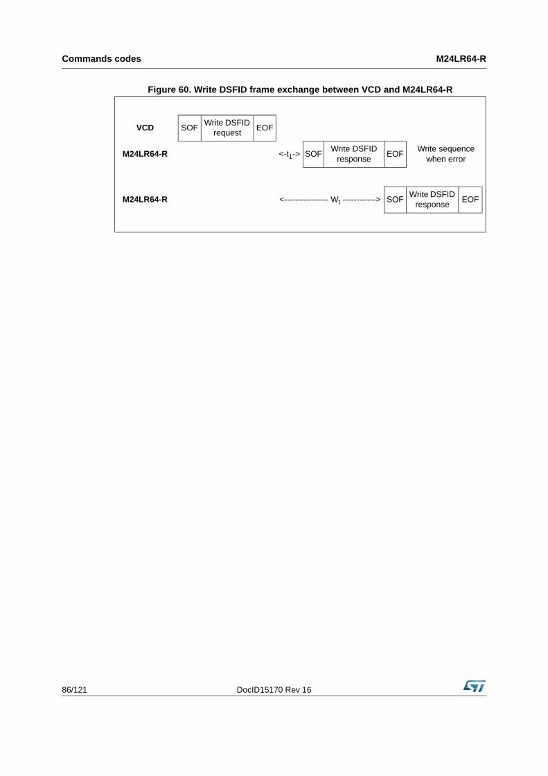
Commands codes M24LR64-R
86/121 DocID15170 Rev 16
Figure 60. Write DSFID frame exchange between VCD and M24LR64-R
VCD SOFWrite DSFID
requestEOF
M24LR64-R <-t1-> SOFWrite DSFID
responseEOF
Write sequence when error
M24LR64-R <---------------- Wt ------------> SOFWrite DSFID
responseEOF
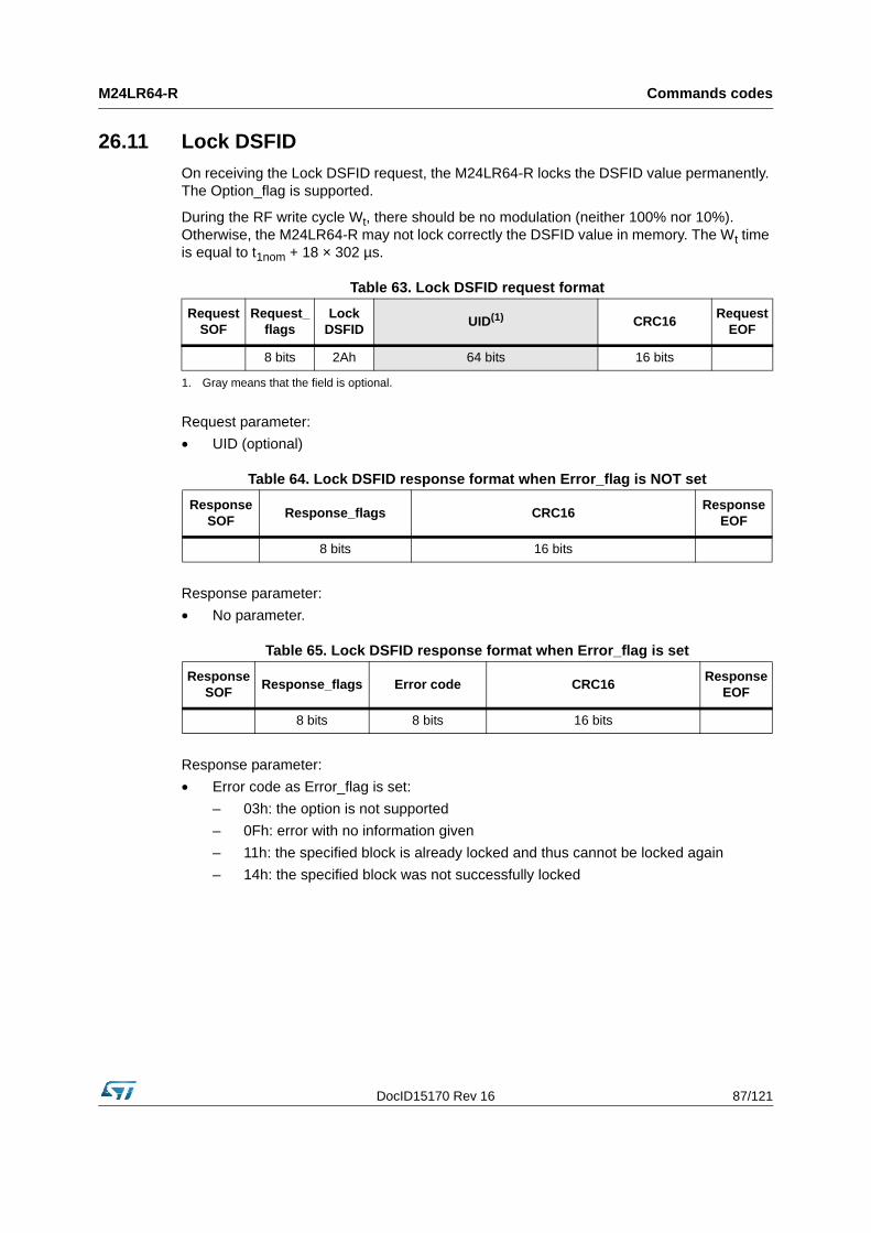
DocID15170 Rev 16 87/121
M24LR64-R Commands codes
26.11 Lock DSFID
On receiving the Lock DSFID request, the M24LR64-R locks the DSFID value permanently. The Option_flag is supported.
During the RF write cycle Wt, there should be no modulation (neither 100% nor 10%). Otherwise, the M24LR64-R may not lock correctly the DSFID value in memory. The Wt time is equal to t1nom + 18 × 302 µs.
Request parameter:
• UID (optional)
Response parameter:
• No parameter.
Response parameter:
• Error code as Error_flag is set:
– 03h: the option is not supported
– 0Fh: error with no information given
– 11h: the specified block is already locked and thus cannot be locked again
– 14h: the specified block was not successfully locked
Table 63. Lock DSFID request format
Request SOF
Request_flags
Lock DSFID
UID(1)
1. Gray means that the field is optional.
CRC16Request
EOF
8 bits 2Ah 64 bits 16 bits
Table 64. Lock DSFID response format when Error_flag is NOT set
Response SOF
Response_flags CRC16Response
EOF
8 bits 16 bits
Table 65. Lock DSFID response format when Error_flag is set
Response SOF
Response_flags Error code CRC16Response
EOF
8 bits 8 bits 16 bits

Commands codes M24LR64-R
88/121 DocID15170 Rev 16
26.12 Get System Info
When receiving the Get System Info command, the M24LR64-R sends back its information data in the response.The Option_flag is supported and must be reset to 0. The Get System Info can be issued in both Addressed and Non Addressed modes.The Protocol_extention_flag should be set to 1 for the M24LR64-R to operate correctly. If the Protocol_extention_flag is at 0, the M24LR64-R answers with an error code.
Request parameter:
• UID (optional)
Response parameters:
• Information flags set to 0Fh. DSFID, AFI, Memory Size and IC reference fields are present
• UID code on 64 bits
• DSFID value
• AFI value
• Memory size. The M24LR64-R provides 2048 blocks (07FFh) of 4 byte (03h)
• IC reference. Only the 6 MSB are significant.
Figure 61. Lock DSFID frame exchange between VCD and M24LR64-R
VCD SOFLock DSFID
requestEOF
M24LR64-R <-t1-> SOFLock DSFID
responseEOF
Lock sequence when error
M24LR64-R <----------------- Wt -------------> SOFLock
DSFID response
EOF
Table 66. Get System Info request format
Request SOF
Request_flags
Get System Info
UID(1)
1. Gray means that the field is optional.
CRC16Request
EOF
8 bits 2Bh 64 bits 16 bits
Table 67. Get System Info response format when Error_flag is NOT set
Response SOF
Response_flags
Information flags
UID DSFID AFIMemory
SizeIC
referenceCRC16
Response EOF
00h 0Fh 64 bits 8 bits 8 bits 0307FFh 2Ch 16 bits

DocID15170 Rev 16 89/121
M24LR64-R Commands codes
Response parameter:
• Error code as Error_flag is set:
– 03h: Option not supported
– 0Fh: other error
26.13 Get Multiple Block Security Status
When receiving the Get Multiple Block Security Status command, the M24LR64-R sends back the sector security status. The blocks are numbered from '00h to '07FFh' in the request and the value is minus one (–1) in the field. For example, a value of '06' in the “Number of blocks” field requests to return the security status of 7 blocks.
The Protocol_extention_flag should be set to 1 for the M24LR64-R to operate correctly. If the Protocol_extention_flag is at 0, the M24LR64-R answers with an error code.
During the M24LR64-R response, if the internal block address counter reaches 07FFh, it rolls over to 0000h and the Sector Security Status bytes for that location are sent back to the reader.
Request parameter:
• UID (optional)
• First block number
• Number of blocks
Table 68. Get System Info response format when Error_flag is set
Response SOF
Response_flags Error code CRC16Response
EOF
01h 8 bits 16 bits
Figure 62. Get System Info frame exchange between VCD and M24LR64-R
VCD SOFGet System Info
requestEOF
M24LR64-R <-t1-> SOF Get System Info response EOF
Table 69. Get Multiple Block Security Status request format
Request SOF
Request_flags
Get Multiple Block
Security Status
UID(1)
1. Gray means that the field is optional.
First block
number
Number of
blocksCRC16
Request EOF
8 bits 2Ch 64 bits 16 bits 16 bits 16 bits
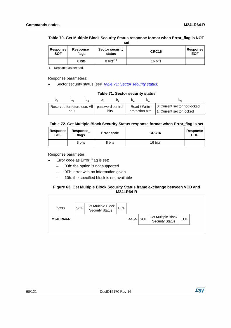
Commands codes M24LR64-R
90/121 DocID15170 Rev 16
Response parameters:
• Sector security status (see Table 71: Sector security status)
Response parameter:
• Error code as Error_flag is set:
– 03h: the option is not supported
– 0Fh: error with no information given
– 10h: the specified block is not available
Table 70. Get Multiple Block Security Status response format when Error_flag is NOT set
Response SOF
Response_flags
Sector security status
CRC16Response
EOF
8 bits 8 bits(1)
1. Repeated as needed.
16 bits
Table 71. Sector security status
b7 b6 b5 b4 b3 b2 b1 b0
Reserved for future use. All at 0
password control bits
Read / Write protection bits
0: Current sector not locked
1: Current sector locked
Table 72. Get Multiple Block Security Status response format when Error_flag is set
Response SOF
Response_flags
Error code CRC16Response
EOF
8 bits 8 bits 16 bits
Figure 63. Get Multiple Block Security Status frame exchange between VCD and M24LR64-R
VCD SOFGet Multiple Block
Security StatusEOF
M24LR64-R <-t1-> SOFGet Multiple Block
Security StatusEOF
DocID15170 Rev 16 91/121
M24LR64-R Commands codes
26.14 Write-sector Password
On receiving the Write-sector Password command, the M24LR64-R uses the data contained in the request to write the password and reports whether the operation was successful in the response. The Option_flag is supported.
During the RF write cycle time, Wt, there must be no modulation at all (neither 100% nor 10%). Otherwise, the M24LR64-R may not correctly program the data into the memory. The Wt time is equal to t1nom + 18 × 302 µs. After a successful write, the new value of the selected password is automatically activated. It is not required to present the new password value until M24LR64-R power-down.
Request parameter:
• UID (optional)
• Password number (01h = Pswd1, 02h = Pswd2, 03h = Pswd3, other = Error)
• Data
Response parameter:
• 32-bit password value. The response is sent back after the write cycle.
Response parameter:
• Error code as Error_flag is set:
– 02h: the command is not recognized, for example: a format error occurred
– 03h: the option is not supported
– 0Fh: error with no information given
– 10h: the specified block is not available
– 12h: the specified block is locked and its contents cannot be changed.
– 13h: the specified block was not successfully programmed
Table 73. Write-sector Password request format
Request SOF
Request_flags
Write-sector
Password
IC Mfg code
UID(1)
1. Gray means that the field is optional.
Password number
Data CRC16Request
EOF
8 bits B1h 02h 64 bits 8 bits 32 bits 16 bits
Table 74. Write-sector Password response format when Error_flag is NOT set
Response SOF
Response_flags CRC16Response
EOF
8 bits 16 bits
Table 75. Write-sector Password response format when Error_flag is set
Response SOF
Response_flags
Error code CRC16Response
EOF
8 bits 8 bits 16 bits

Commands codes M24LR64-R
92/121 DocID15170 Rev 16
26.15 Lock-sector Password
On receiving the Lock-sector Password command, the M24LR64-R sets the access rights and permanently locks the selected sector. The Option_flag is supported.
A sector is selected by giving the address of one of its blocks in the Lock-sector Password request (Sector number field). For example, addresses 0 to 31 are used to select sector 0 and addresses 32 to 63 are used to select sector 1. Care must be taken when issuing the Lock-sector Password command as all the blocks belonging to the same sector are automatically locked by a single command.
The Protocol_extention_flag should be set to 1 for the M24LR64-R to operate correctly. If the Protocol_extention_flag is at 0, the M24LR64-R answers with an error code.
During the RF write cycle Wt, there should be no modulation (neither 100% nor 10%) otherwise, the M24LR64-R may not correctly lock the memory block.The Wt time is equal to t1nom + 18 × 302 µs.
Request parameters:
• (optional) UID
• Sector number
• Sector security status (refer to Table 77)
Figure 64. Write-sector Password frame exchange between VCD and M24LR64-R
VCD SOF
Write-sector
Password request
EOF
M24LR64-R <-t1-> SOFWrite-sector Password response
EOFWrite sequence
when error
M24LR64-R <----------------- Wt -------------> SOF
Write-sector
Password response
EOF
Table 76. Lock-sector Password request format
Request SOF
Request_flags
Lock-sector
Password
IC Mfg code
UID(1)
1. Gray means that the field is optional.
Sector number
Sector security status
CRC16Request
EOF
8 bits B2h 02h 64 bits 16 bits 8 bits 16 bits
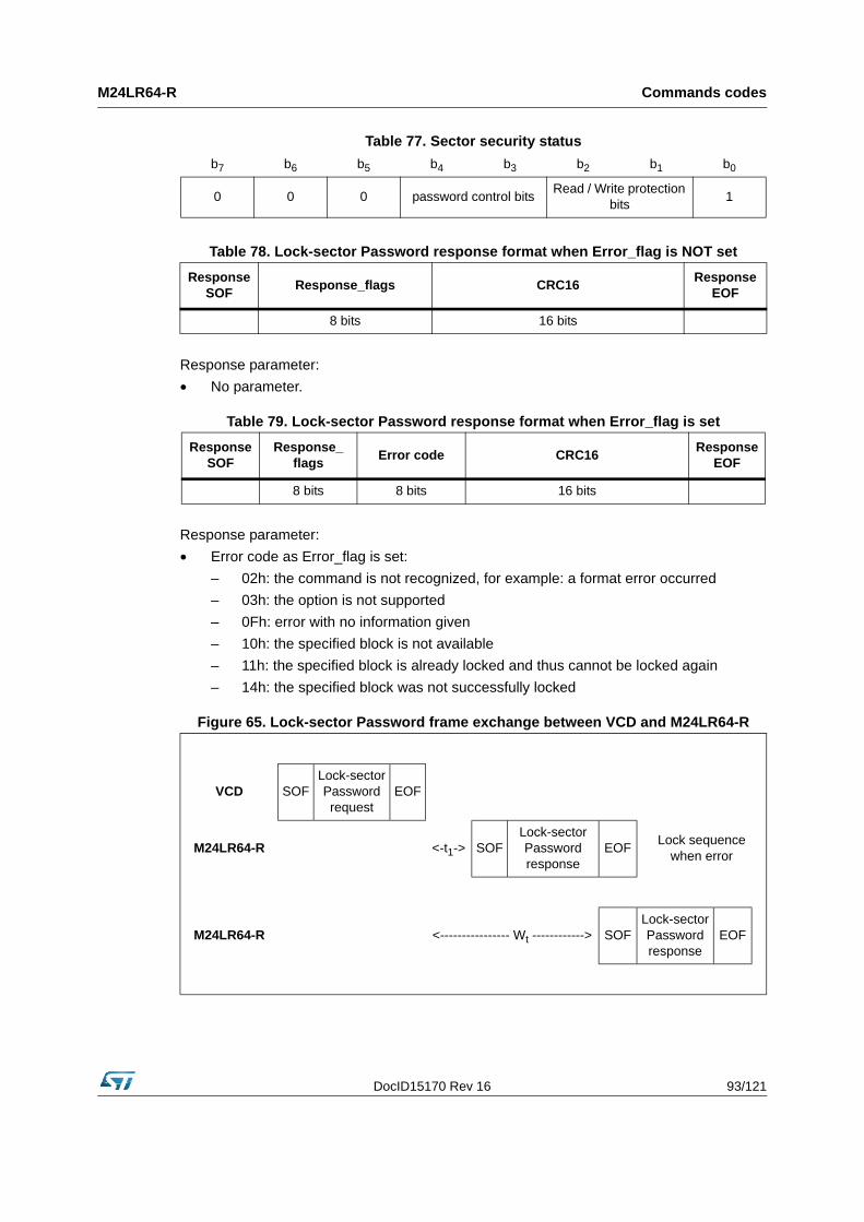
DocID15170 Rev 16 93/121
M24LR64-R Commands codes
Response parameter:
• No parameter.
Response parameter:
• Error code as Error_flag is set:
– 02h: the command is not recognized, for example: a format error occurred
– 03h: the option is not supported
– 0Fh: error with no information given
– 10h: the specified block is not available
– 11h: the specified block is already locked and thus cannot be locked again
– 14h: the specified block was not successfully locked
Table 77. Sector security status
b7 b6 b5 b4 b3 b2 b1 b0
0 0 0 password control bitsRead / Write protection
bits1
Table 78. Lock-sector Password response format when Error_flag is NOT set
Response SOF
Response_flags CRC16Response
EOF
8 bits 16 bits
Table 79. Lock-sector Password response format when Error_flag is set
Response SOF
Response_flags
Error code CRC16Response
EOF
8 bits 8 bits 16 bits
Figure 65. Lock-sector Password frame exchange between VCD and M24LR64-R
VCD SOFLock-sector Password request
EOF
M24LR64-R <-t1-> SOFLock-sector Password response
EOFLock sequence
when error
M24LR64-R <---------------- Wt ------------> SOFLock-sector Password response
EOF

Commands codes M24LR64-R
94/121 DocID15170 Rev 16
26.16 Present-sector Password
On receiving the Present-sector Password command, the M24LR64-R compares the requested password with the data contained in the request and reports whether the operation has been successful in the response. The Option_flag is supported.During the comparison cycle equal to Wt, there should be no modulation (neither 100% nor 10%) otherwise, the M24LR64-R the Password value may not be correctly compared.The Wt time is equal to t1nom + 18 × 302 µs.After a successful command, the access to all the memory blocks linked to the password is changed as described in Section 4.1: M24LR64-R RF block security.
Request parameter:
• UID (optional)
• Password Number (0x01 = Pswd1, 0x02 = Pswd2, 0x03 = Pswd3, other = Error)
• Data
Response parameter:
• No parameter. The response is send back after the write cycle.
Response parameter:
• Error code as Error_flag is set:
– 02h: the command is not recognized, for example: a format error occurred
– 03h: the option is not supported
– 0Fh: error with no information given
– 10h: the specified block is not available
Table 80. Present-sector Password request format
Request SOF
Request_flags
Present-sector
Password
IC Mfg code
UID(1)
1. Gray means that the field is optional.
Password number
Data CRC16Request
EOF
8 bits B3h 02h 64 bits 8 bits 32 bits 16 bits
Table 81. Present-sector Password response format when Error_flag is NOT set
Response SOF
Response_flags CRC16Response
EOF
8 bits 16 bits
Table 82. Present-sector Password response format when Error_flag is set
Response SOF
Response_flags
Error code CRC16Response
EOF
8 bits 8 bits 16 bits

DocID15170 Rev 16 95/121
M24LR64-R Commands codes
26.17 Fast Read Single Block
On receiving the Fast Read Single Block command, the M24LR64-R reads the requested block and sends back its 32-bit value in the response. The Option_flag is supported. The data rate of the response is multiplied by 2.
The Protocol_extention_flag should be set to 1 for the M24LR64-R to operate correctly. If the Protocol_extention_flag is at 0, the M24LR64-R answers with an error code.
Request parameters:
• Option_flag
• UID (optional)
• Block number
Figure 66. Present-sector Password frame exchange between VCD and M24LR64-R
VCD SOF
Present-sector
Password request
EOF
M24LR64-R <-t1-> SOF
Present-sector
Password response
EOF sequence when
error
M24LR64-R <---------------- Wt ------------> SOF
Present-sector
Password response
EOF
Table 83. Fast Read Single Block request format
Request SOF
Request_flags
Fast Read Single Block
IC Mfg code
UID(1)
1. Gray means that the field is optional.
Block number
CRC16Request
EOF
8 bits C0h 02h 64 bits 16 bits 16 bits
Table 84. Fast Read Single Block response format when Error_flag is NOT set
Response SOF
Response_flags
Sector security status(1)
1. Gray means that the field is optional.
Data CRC16Response
EOF
8 bits 8 bits 32 bits 16 bits

Commands codes M24LR64-R
96/121 DocID15170 Rev 16
Response parameters:
• Sector security status if Option_flag is set (see Table 85)
• 4 bytes of block data
Response parameter:
• Error code as Error_flag is set:
– 02h: the command is not recognized, for example: a format error occurred
– 03h: the option is not supported
– 0Fh: error with no information given
– 10h: the specified block is not available
– 15h: the specified block is read protected
Table 85. Sector security status
b7 b6 b5 b4 b3 b2 b1 b0
Reserved for future used. All at 0
password control bits
Read / Write protection bits
0: Current sector not locked
1: Current sector locked
Table 86. Fast Read Single Block response format when Error_flag is set
Response SOF
Response_flags
Error code CRC16Response
EOF
8 bits 8 bits 16 bits
Figure 67. Fast Read Single Block frame exchange between VCD and M24LR64-R
VCD SOFFast Read Single
Block requestEOF
M24LR64-R <-t1-> SOFFast Read Single Block response
EOF

DocID15170 Rev 16 97/121
M24LR64-R Commands codes
26.18 Fast Inventory Initiated
Before receiving the Fast Inventory Initiated command, the M24LR64-R must have received an Initiate or a Fast Initiate command in order to set the Initiate_ flag. If not, the M24LR64-R does not answer to the Fast Inventory Initiated command.On receiving the Fast Inventory Initiated request, the M24LR64-R runs the anticollision sequence. The Inventory_flag must be set to 1. The meaning of flags 5 to 8 is shown in Table 26: Request flags 5 to 8 when Bit 3 = 1. The data rate of the response is multiplied by 2.
The request contains:
• the flags,
• the Inventory command code
• the AFI if the AFI flag is set
• the mask length
• the mask value
• the CRC
The M24LR64-R does not generate any answer in case of error.
The Response contains:
• the flags
• the Unique ID
During an Inventory process, if the VCD does not receive an RF M24LR64-R response, it waits a time t3 before sending an EOF to switch to the next slot. t3 starts from the rising edge of the request EOF sent by the VCD.
• If the VCD sends a 100% modulated EOF, the minimum value of t3 is:t3min = 4384/fC (323.3 µs) + tSOF
• If the VCD sends a 10% modulated EOF, the minimum value of t3 is:t3min = 4384/fC (323.3 µs) + tNRT
where:
• tSOF is the time required by the M24LR64-R to transmit an SOF to the VCD
• tNRT is the nominal response time of the M24LR64-R
Table 87. Fast Inventory Initiated request format
Request SOF
Request_flags
Fast Inventory Initiated
IC Mfg code
Optional AFI
Mask length
Mask value CRC16Request
EOF
8 bits C1h 02h 8 bits 8 bits 0 - 64 bits 16 bits
Table 88. Fast Inventory Initiated response format
Response SOF
Response_flags
DSFID UID CRC16Response
EOF
8 bits 8 bits 64 bits 16 bits
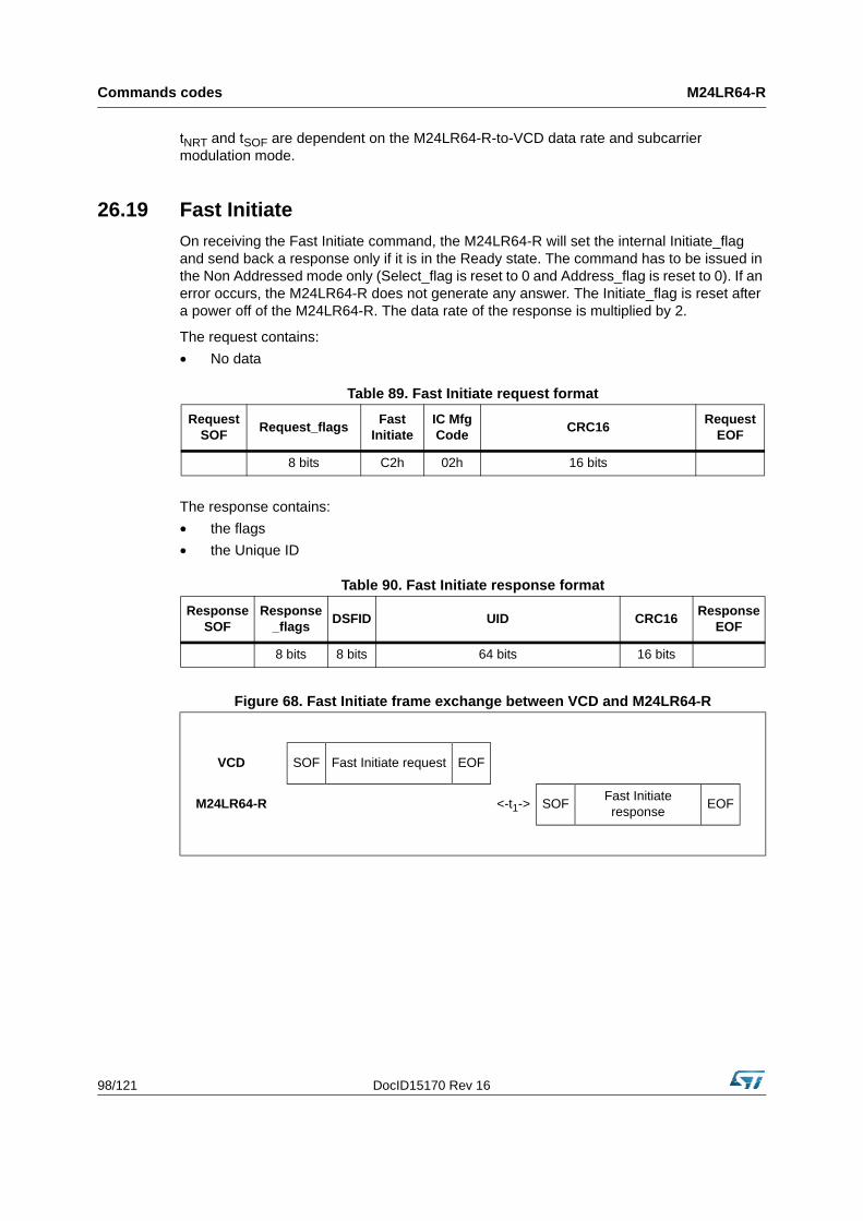
Commands codes M24LR64-R
98/121 DocID15170 Rev 16
tNRT and tSOF are dependent on the M24LR64-R-to-VCD data rate and subcarrier modulation mode.
26.19 Fast Initiate
On receiving the Fast Initiate command, the M24LR64-R will set the internal Initiate_flag and send back a response only if it is in the Ready state. The command has to be issued in the Non Addressed mode only (Select_flag is reset to 0 and Address_flag is reset to 0). If an error occurs, the M24LR64-R does not generate any answer. The Initiate_flag is reset after a power off of the M24LR64-R. The data rate of the response is multiplied by 2.
The request contains:
• No data
The response contains:
• the flags
• the Unique ID
Table 89. Fast Initiate request format
Request SOF
Request_flagsFast
InitiateIC Mfg Code
CRC16Request
EOF
8 bits C2h 02h 16 bits
Table 90. Fast Initiate response format
Response SOF
Response_flags
DSFID UID CRC16Response
EOF
8 bits 8 bits 64 bits 16 bits
Figure 68. Fast Initiate frame exchange between VCD and M24LR64-R
VCD SOF Fast Initiate request EOF
M24LR64-R <-t1-> SOFFast Initiate response
EOF
DocID15170 Rev 16 99/121
M24LR64-R Commands codes
26.20 Fast Read Multiple Block
On receiving the Fast Read Multiple Block command, the M24LR64-R reads the selected blocks and sends back their value in multiples of 32 bits in the response. The blocks are numbered from '00h to '7FFh' in the request and the value is minus one (–1) in the field. For example, if the “number of blocks” field contains the value 06h, 7 blocks are read. The maximum number of blocks is fixed to 32 assuming that they are all located in the same sector. If the number of blocks overlaps sectors, the M24LR64-R returns an error code.
The Protocol_extention_flag should be set to 1 for the M24LR64-R to operate correctly. If the Protocol_extention_flag is at 0, the M24LR64-R answers with an error code.
The Option_flag is supported. The data rate of the response is multiplied by 2.
Request parameters:
• Option_flag
• UID (Optional)
• First block number
• Number of blocks
Response parameters:
• Sector security status if Option_flag is set (see Table 93: Sector security status if Option_flag is set)
• N block of data
Table 91. Fast Read Multiple Block request format
Request SOF
Request_flags
Fast Read
Multiple Block
IC Mfg code
UID(1)
1. Gray means that the field is optional.
First block
number
Number of
blocksCRC16
Request EOF
8 bits C3h 02h 64 bits 16 bits 8 bits 16 bits
Table 92. Fast Read Multiple Block response format when Error_flag is NOT set
Response SOF
Response_flags
Sector security status(1)
1. Gray means that the field is optional.
Data CRC16Response
EOF
8 bits 8 bits(2)
2. Repeated as needed.
32 bits(2) 16 bits
Table 93. Sector security status if Option_flag is set
b7 b6 b5 b4 b3 b2 b1 b0
Reserved for future use. All at 0
password control bits
Read / Write protection bits
0: Current sector not locked1: Current sector locked
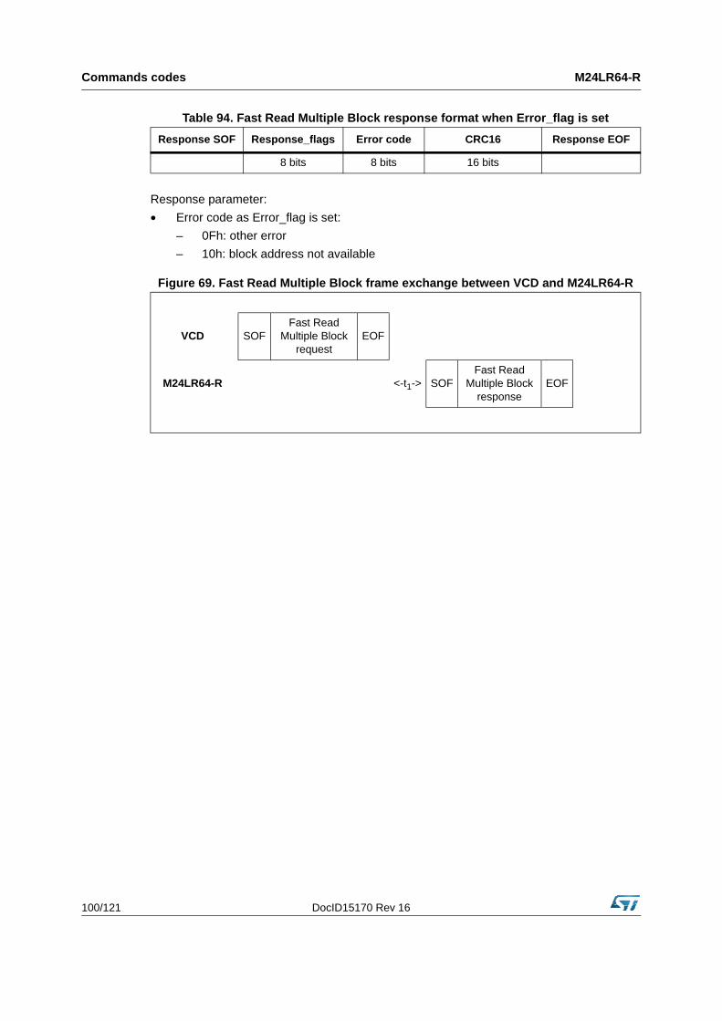
Commands codes M24LR64-R
100/121 DocID15170 Rev 16
Response parameter:
• Error code as Error_flag is set:
– 0Fh: other error
– 10h: block address not available
Table 94. Fast Read Multiple Block response format when Error_flag is set
Response SOF Response_flags Error code CRC16 Response EOF
8 bits 8 bits 16 bits
Figure 69. Fast Read Multiple Block frame exchange between VCD and M24LR64-R
VCD SOFFast Read
Multiple Block request
EOF
M24LR64-R <-t1-> SOFFast Read
Multiple Block response
EOF
DocID15170 Rev 16 101/121
M24LR64-R Commands codes
26.21 Inventory Initiated
Before receiving the Inventory Initiated command, the M24LR64-R must have received an Initiate or a Fast Initiate command in order to set the Initiate_ flag. If not, the M24LR64-R does not answer to the Inventory Initiated command.
On receiving the Inventory Initiated request, the M24LR64-R runs the anticollision sequence. The Inventory_flag must be set to 1. The meaning of flags 5 to 8 is given in Table 26: Request flags 5 to 8 when Bit 3 = 1.
The request contains:
• the flags,
• the Inventory Command code
• the AFI if the AFI flag is set
• the mask length
• the mask value
• the CRC
The M24LR64-R does not generate any answer in case of error.
The response contains:
• the flags
• the Unique ID
During an Inventory process, if the VCD does not receive an RF M24LR64-R response, it waits a time t3 before sending an EOF to switch to the next slot. t3 starts from the rising edge of the request EOF sent by the VCD.
• If the VCD sends a 100% modulated EOF, the minimum value of t3 is:t3min = 4384/fC (323.3 µs) + tSOF
• If the VCD sends a 10% modulated EOF, the minimum value of t3 is:t3min = 4384/fC (323.3 µs) + tNRT
where:
• tSOF is the time required by the M24LR64-R to transmit an SOF to the VCD
• tNRT is the nominal response time of the M24LR64-R
tNRT and tSOF are dependent on the M24LR64-R-to-VCD data rate and subcarrier modulation mode.
Table 95. Inventory Initiated request format
Request SOF
Request_flags
Inventory Initiated
IC Mfg
code
Optional AFI
Mask length
Mask value CRC16Request
EOF
8 bits D1h 02h 8 bits 8 bits 0 - 64 bits 16 bits
Table 96. Inventory Initiated response format
Response SOF
Response_flags
DSFID UID CRC16Response
EOF
8 bits 8 bits 64 bits 16 bits

Commands codes M24LR64-R
102/121 DocID15170 Rev 16
26.22 Initiate
On receiving the Initiate command, the M24LR64-R will set the internal Initiate_flag and send back a response only if it is in the ready state. The command has to be issued in the Non Addressed mode only (Select_flag is reset to 0 and Address_flag is reset to 0). If an error occurs, the M24LR64-R does not generate any answer. The Initiate_flag is reset after a power off of the M24LR64-R.
The request contains:
• No data
The response contains:
• the flags
• the Unique ID
Table 97. Initiate request format
Request SOF
Request_flags InitiateIC Mfg code
CRC16Request
EOF
8 bits D2h 02h 16 bits
Table 98. Initiate Initiated response format
Response SOF
Response_flags
DSFID UID CRC16Response
EOF
8 bits 8 bits 64 bits 16 bits

DocID15170 Rev 16 103/121
M24LR64-R Commands codes
Figure 70. Initiate frame exchange between VCD and M24LR64-R
VCD SOFInitiate request
EOF
M24LR64-R <-t1-> SOFInitiate
responseEOF
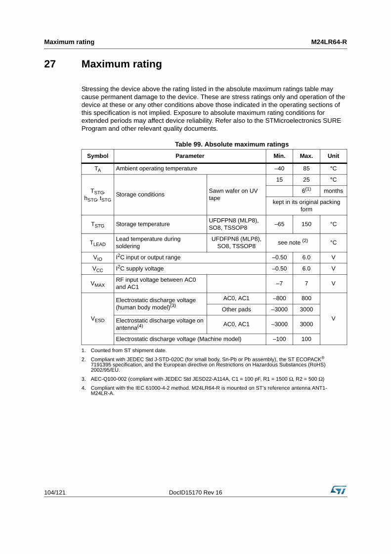
Maximum rating M24LR64-R
104/121 DocID15170 Rev 16
27 Maximum rating
Stressing the device above the rating listed in the absolute maximum ratings table may cause permanent damage to the device. These are stress ratings only and operation of the device at these or any other conditions above those indicated in the operating sections of this specification is not implied. Exposure to absolute maximum rating conditions for extended periods may affect device reliability. Refer also to the STMicroelectronics SURE Program and other relevant quality documents.
Table 99. Absolute maximum ratings
Symbol Parameter Min. Max. Unit
TA Ambient operating temperature –40 85 °C
TSTG, hSTG, tSTG
Storage conditionsSawn wafer on UV tape
15 25 °C
6(1)
1. Counted from ST shipment date.
months
kept in its original packing form
TSTG Storage temperatureUFDFPN8 (MLP8), SO8, TSSOP8
–65 150 °C
TLEADLead temperature during soldering
UFDFPN8 (MLP8), SO8, TSSOP8
see note (2)
2. Compliant with JEDEC Std J-STD-020C (for small body, Sn-Pb or Pb assembly), the ST ECOPACK® 7191395 specification, and the European directive on Restrictions on Hazardous Substances (RoHS) 2002/95/EU.
°C
VIO I2C input or output range –0.50 6.0 V
VCC I2C supply voltage –0.50 6.0 V
VMAXRF input voltage between AC0 and AC1
–7 7 V
VESD
Electrostatic discharge voltage (human body model)(3)
3. AEC-Q100-002 (compliant with JEDEC Std JESD22-A114A, C1 = 100 pF, R1 = 1500 Ω, R2 = 500 Ω)
AC0, AC1 –800 800
V
Other pads –3000 3000
Electrostatic discharge voltage on antenna(4)
4. Compliant with the IEC 61000-4-2 method. M24LR64-R is mounted on ST’s reference antenna ANT1-M24LR-A.
AC0, AC1 –3000 3000
Electrostatic discharge voltage (Machine model) –100 100
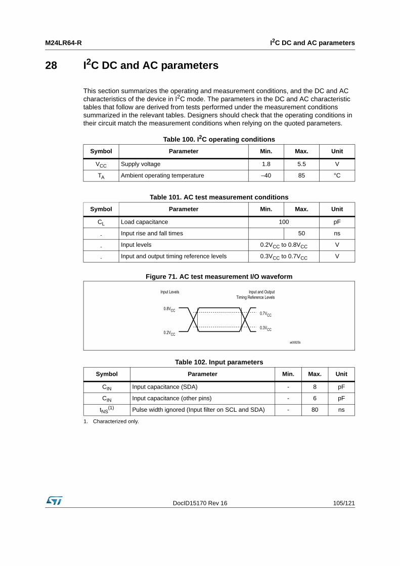
DocID15170 Rev 16 105/121
M24LR64-R I2C DC and AC parameters
28 I2C DC and AC parameters
This section summarizes the operating and measurement conditions, and the DC and AC characteristics of the device in I2C mode. The parameters in the DC and AC characteristic tables that follow are derived from tests performed under the measurement conditions summarized in the relevant tables. Designers should check that the operating conditions in their circuit match the measurement conditions when relying on the quoted parameters.
Figure 71. AC test measurement I/O waveform
Table 100. I2C operating conditions
Symbol Parameter Min. Max. Unit
VCC Supply voltage 1.8 5.5 V
TA Ambient operating temperature –40 85 °C
Table 101. AC test measurement conditions
Symbol Parameter Min. Max. Unit
CL Load capacitance 100 pF
- Input rise and fall times 50 ns
- Input levels 0.2VCC to 0.8VCC V
- Input and output timing reference levels 0.3VCC to 0.7VCC V
Table 102. Input parameters
Symbol Parameter Min. Max. Unit
CIN Input capacitance (SDA) - 8 pF
CIN Input capacitance (other pins) - 6 pF
tNS(1)
1. Characterized only.
Pulse width ignored (Input filter on SCL and SDA) - 80 ns
ai00825b
0.8VCC
0.2VCC
0.7VCC
0.3VCC
Input and OutputTiming Reference Levels
Input Levels

I2C DC and AC parameters M24LR64-R
106/121 DocID15170 Rev 16
Table 103. I2C DC characteristics
Symbol Parameter Test condition Min. Max. Unit
ILIInput leakage current (SCL, SDA, E1, E0)
VIN = VSS or VCCdevice in Standby mode
- ± 2 µA
ILO Output leakage currentSDA in Hi-Z, external voltage applied on SDA: VSS or VCC
- ± 2 µA
ICC Supply current (Read)(1)
1. SCL, SDA according to AC input waveform Figure 71. E0, E1 connected to Ground or VCC
VCC = 1.8 V, fc = 400 kHz(rise/fall time < 50 ns)
- 100
µAVCC = 2.5 V, fc = 400 kHz
(rise/fall time < 50 ns)- 200
VCC = 5.5 V, fc = 400 kHz(rise/fall time < 50 ns)
- 500
ICC0 Supply current (Write)(1)
During tW, VCC = 1.8 V - 300(2)
2. Characterized value, not tested in production.
µADuring tW, VCC = 2.5 V - 400(2)
During tW, VCC = 5.5 V - 700(2)
ICC1 Standby supply current
VIN = VSS or VCC
VCC = 1.8 V- 30
µAVIN = VSS or VCC
VCC = 2.5 V- 30
VIN = VSS or VCC
VCC = 5.5 V- 40
VILInput low voltage (SDA, SCL)
VCC = 1.8 V –0.45 0.25VCC
VVCC = 2.5 V –0.45 0.25VCC
VCC = 5.5 V –0.45 0.3VCC
VIHInput high voltage (SDA, SCL)
VCC = 1.8 V 0.75VCC VCC+1
VVCC = 2.5 V 0.75VCC VCC+1
VCC = 5.5 V 0.7VCC VCC+1
VOL Output low voltageIOL = 2.1 mA, VCC = 1.8 V or
IOL = 3 mA, VCC = 5.5 V- 0.4 V
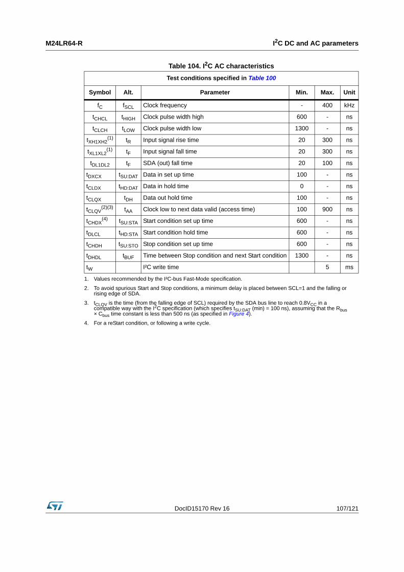
DocID15170 Rev 16 107/121
M24LR64-R I2C DC and AC parameters
Table 104. I2C AC characteristics
Test conditions specified in Table 100
Symbol Alt. Parameter Min. Max. Unit
fC fSCL Clock frequency - 400 kHz
tCHCL tHIGH Clock pulse width high 600 - ns
tCLCH tLOW Clock pulse width low 1300 - ns
tXH1XH2(1)
1. Values recommended by the I²C-bus Fast-Mode specification.
tR Input signal rise time 20 300 ns
tXL1XL2(1) tF Input signal fall time 20 300 ns
tDL1DL2 tF SDA (out) fall time 20 100 ns
tDXCX tSU:DAT Data in set up time 100 - ns
tCLDX tHD:DAT Data in hold time 0 - ns
tCLQX tDH Data out hold time 100 - ns
tCLQV(2)(3)
2. To avoid spurious Start and Stop conditions, a minimum delay is placed between SCL=1 and the falling or rising edge of SDA.
3. tCLQV is the time (from the falling edge of SCL) required by the SDA bus line to reach 0.8VCC in a compatible way with the I2C specification (which specifies tSU:DAT (min) = 100 ns), assuming that the Rbus × Cbus time constant is less than 500 ns (as specified in Figure 4).
tAA Clock low to next data valid (access time) 100 900 ns
tCHDX(4)
4. For a reStart condition, or following a write cycle.
tSU:STA Start condition set up time 600 - ns
tDLCL tHD:STA Start condition hold time 600 - ns
tCHDH tSU:STO Stop condition set up time 600 - ns
tDHDL tBUF Time between Stop condition and next Start condition 1300 - ns
tW I²C write time 5 ms
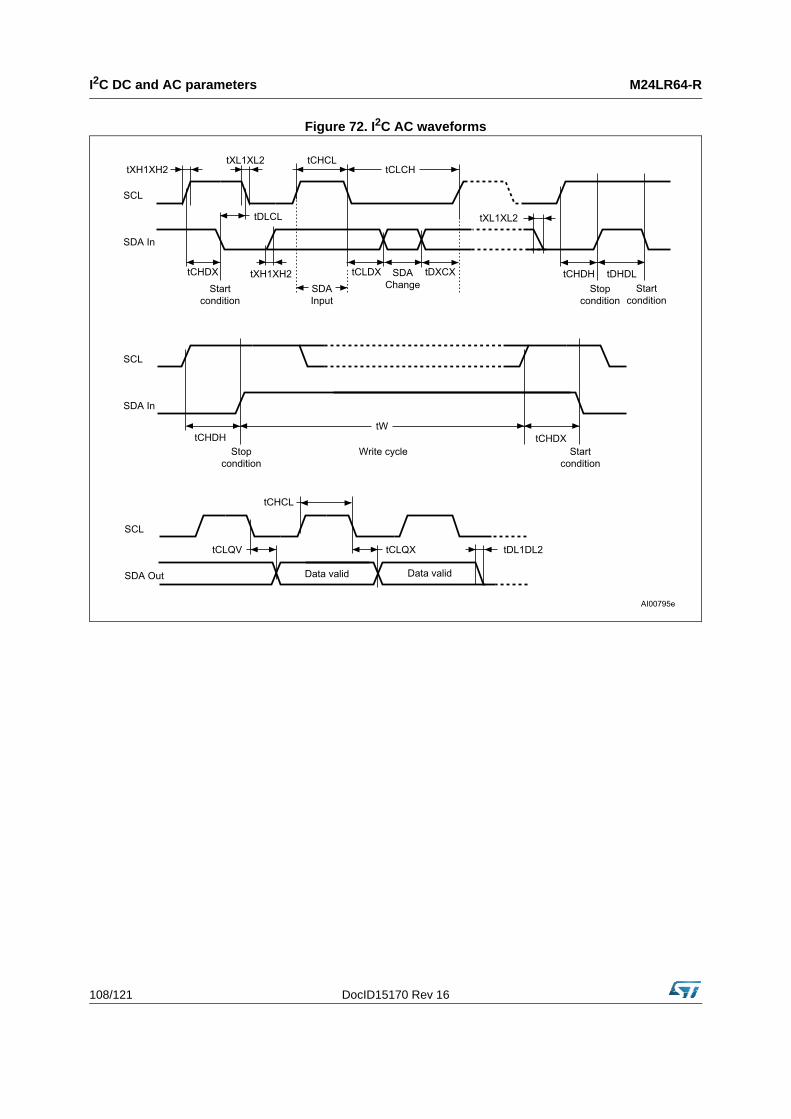
I2C DC and AC parameters M24LR64-R
108/121 DocID15170 Rev 16
Figure 72. I2C AC waveforms
SCL
SDA In
SCL
SDA Out
SCL
SDA In
tCHCL
tDLCL
tCHDX
Startcondition
tCLCH
tDXCXtCLDX
SDAInput
SDAChange
tCHDH tDHDLStop
condition
Data valid
tCLQV tCLQX
tCHDHStop
condition
tCHDXStart
conditionWrite cycle
tW
AI00795e
Startcondition
tCHCL
tXH1XH2
tXH1XH2
tXL1XL2
tXL1XL2
Data valid
tDL1DL2
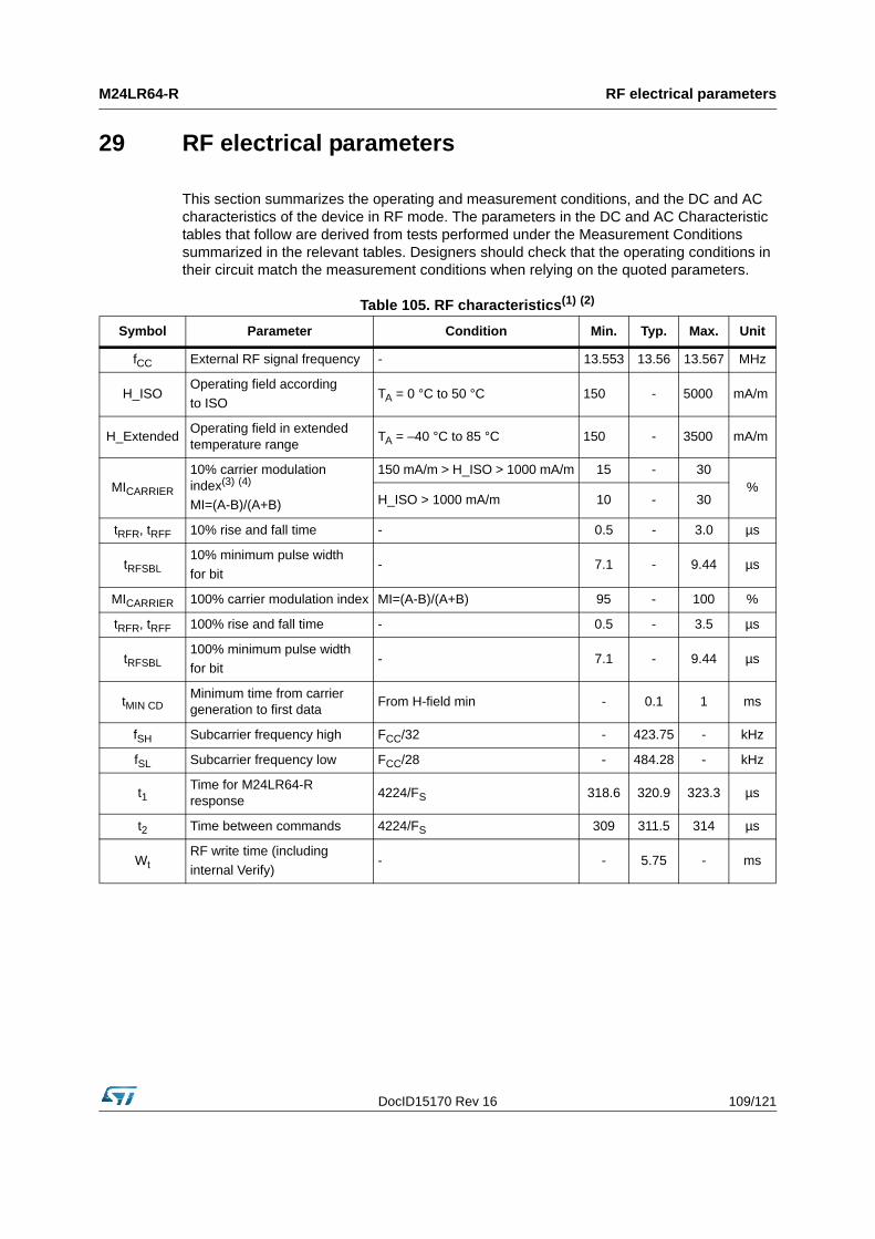
DocID15170 Rev 16 109/121
M24LR64-R RF electrical parameters
29 RF electrical parameters
This section summarizes the operating and measurement conditions, and the DC and AC characteristics of the device in RF mode. The parameters in the DC and AC Characteristic tables that follow are derived from tests performed under the Measurement Conditions summarized in the relevant tables. Designers should check that the operating conditions in their circuit match the measurement conditions when relying on the quoted parameters.
Table 105. RF characteristics(1) (2)
Symbol Parameter Condition Min. Typ. Max. Unit
fCC External RF signal frequency - 13.553 13.56 13.567 MHz
H_ISOOperating field according
to ISOTA = 0 °C to 50 °C 150 - 5000 mA/m
H_ExtendedOperating field in extended temperature range
TA = –40 °C to 85 °C 150 - 3500 mA/m
MICARRIER
10% carrier modulation index(3) (4)
MI=(A-B)/(A+B)
150 mA/m > H_ISO > 1000 mA/m 15 - 30%
H_ISO > 1000 mA/m 10 - 30
tRFR, tRFF 10% rise and fall time - 0.5 - 3.0 µs
tRFSBL10% minimum pulse width
for bit- 7.1 - 9.44 µs
MICARRIER 100% carrier modulation index MI=(A-B)/(A+B) 95 - 100 %
tRFR, tRFF 100% rise and fall time - 0.5 - 3.5 µs
tRFSBL100% minimum pulse width
for bit- 7.1 - 9.44 µs
tMIN CDMinimum time from carrier generation to first data
From H-field min - 0.1 1 ms
fSH Subcarrier frequency high FCC/32 - 423.75 - kHz
fSL Subcarrier frequency low FCC/28 - 484.28 - kHz
t1Time for M24LR64-R response
4224/FS 318.6 320.9 323.3 µs
t2 Time between commands 4224/FS 309 311.5 314 µs
WtRF write time (including
internal Verify)- - 5.75 - ms

RF electrical parameters M24LR64-R
110/121 DocID15170 Rev 16
Figure 73 shows an ASK modulated signal, from the VCD to the M24LR64-R. The test condition for the AC/DC parameters are:
• Close coupling condition with tester antenna (1 mm)
• M24LR64-R performance measured at the tag antenna
Figure 73. M24LR64-R synchronous timing, transmit and receive
CTUNInternal tuning capacitor in SO8(5) f = 13.56 MHz 24.8 27.5 30.2 pF
VBACKBackscattered level as defined
by ISO testISO10373-7 10 - - mV
VMINMinimum operating voltage between AC0 and AC1(6)
Inventory and Read operations - 1.9 2.3 Vpeak
Write operations - 2.3 2.6 Vpeak
1. TA = –40 to 85 °C.
2. All timing measurements were performed between 0 °C and 50 °C on a reference antenna with the following characteristics:External size: 75 mm x 48 mmNumber of turns: 5Width of conductor: 0.5 mmSpace between 2 conductors: 0.3 mmValue of the tuning capacitor in SO8: 27.5 pF (M24LR64-R)Value of the coil: 5 µHTuning frequency: 13.56 MHz.
3. Characterized only, not 100% tested
4. 15% (or more) carrier modulation index offers a better signal/noise ratio and therefore a wider operating range with a better noise immunity
5. Characterised only, at room temperature only, measured at VAC0-AC1 = 0.5 V peak.
6. Characterized only, at room temperature only.
Table 105. RF characteristics(1) (2) (continued)
Symbol Parameter Condition Min. Typ. Max. Unit
Table 106. Operating conditions
Symbol Parameter Min. Max. Unit
TA Ambient operating temperature –40 85 °C
AI06680
A BtRFF
tRFR
tRFSBL
tMAX tMIN CD
fCC

DocID15170 Rev 16 111/121
M24LR64-R Package mechanical data
30 Package mechanical data
In order to meet environmental requirements, ST offers these devices in different grades of ECOPACK® packages, depending on their level of environmental compliance. ECOPACK® specifications, grade definitions and product status are available at: www.st.com. ECOPACK® is an ST trademark.
Figure 74. SO8N – 8-lead plastic small outline, 150 mils body width, package outline
1. Drawing is not to scale.
Table 107. SO8N – 8-lead plastic small outline, 150 mils body width, package data
Symbolmillimeters inches(1)
1. Values in inches are converted from mm and rounded to 4 decimal digits.
Typ. Min. Max. Typ. Min. Max.
A 1.75 0.0689
A1 0.10 0.25 0.0039 0.0098
A2 1.25 0.0492
b 0.28 0.48 0.0110 0.0189
c 0.17 0.23 0.0067 0.0091
ccc 0.10 0.0039
D 4.90 4.80 5.00 0.1929 0.1890 0.1969
E 6.00 5.80 6.20 0.2362 0.2283 0.2441
E1 3.90 3.80 4.00 0.1535 0.1496 0.1575
e 1.27 – – 0.0500 – –
h 0.25 0.50
k 0° 8° 0° 8°
L 0.40 1.27 0.0157 0.0500
L1 1.04 0.0410
SO-A
E1
8
cccb
e
A
D
c
1E
h x 45°
A2
k
0.25 mm
L
L1A1
GAUGE PLANE

Package mechanical data M24LR64-R
112/121 DocID15170 Rev 16
Figure 75. UFDFPN8 (MLP8) – Ultra thin fine pitch dual flat package no lead 2 x 3 mm, package outline
1. Drawing is not to scale.
D
E
ZW_MEe
A
A1eee
L1
e b
D2
L
E2
L3 L1
e b
D2
L
E2
L3
Pin 1
KK
MB MC
Table 108. UFDFPN8 (MLP8) – Ultra thin fine pitch dual flat package no lead 2 x 3 mm, package mechanical data
SymbolMillimeters Inches (1)
1. Values in inches are converted from mm and rounded to 4 decimal digits.
Typ. Min. Max. Typ. Min. Max.
A 0.55 0.45 0.60 0.0217 0.0177 0.0236
A1 0.02 0 0.05 0.0008 0 0.0020
b 0.25 0.20 0.30 0.0098 0.0079 0.0118
D 2 1.90 2.10 0.0787 0.0748 0.0827
D2 (MB) 1.60 1.50 1.70 0.0630 0.0591 0.0669
D2 (MC) − 1.20 1.60 − 0.0472 0.0630
E 3 2.90 3.10 0.1181 0.1142 0.1220
E2 (MB) 0.2 0.10 0.30 0.0079 0.0039 0.0118
E2 (MC) − 1.20 1.60 − 0.0472 0.0630
e 0.50 − − 0.0197 − −
K − 0.30 − − 0.0118 −
L − 0.30 0.50 − 0.0118 0.0197
L1 − − 0.15 − − 0.0059
L3 − 0.30 − − 0.0118 −
eee (2)
2. Applied for exposed die paddle and terminals. Exclude embedding part of exposed die paddle from measuring.
0.08 0.0031
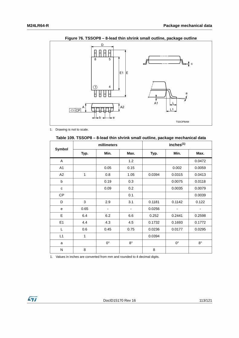
DocID15170 Rev 16 113/121
M24LR64-R Package mechanical data
Figure 76. TSSOP8 – 8-lead thin shrink small outline, package outline
1. Drawing is not to scale.
Table 109. TSSOP8 – 8-lead thin shrink small outline, package mechanical data
Symbolmillimeters inches(1)
1. Values in inches are converted from mm and rounded to 4 decimal digits.
Typ. Min. Max. Typ. Min. Max.
A 1.2 0.0472
A1 0.05 0.15 0.002 0.0059
A2 1 0.8 1.05 0.0394 0.0315 0.0413
b 0.19 0.3 0.0075 0.0118
c 0.09 0.2 0.0035 0.0079
CP 0.1 0.0039
D 3 2.9 3.1 0.1181 0.1142 0.122
e 0.65 - - 0.0256 - -
E 6.4 6.2 6.6 0.252 0.2441 0.2598
E1 4.4 4.3 4.5 0.1732 0.1693 0.1772
L 0.6 0.45 0.75 0.0236 0.0177 0.0295
L1 1 0.0394
a 0° 8° 0° 8°
N 8 8
TSSOP8AM
1
8
CP
c
L
EE1
D
A2A
a
eb
4
5
A1
L1
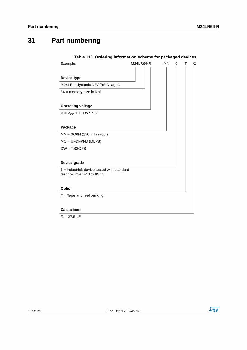
Part numbering M24LR64-R
114/121 DocID15170 Rev 16
31 Part numbering
Table 110. Ordering information scheme for packaged devices
Example: M24LR64-R MN 6 T /2
Device type
M24LR = dynamic NFC/RFID tag IC
64 = memory size in Kbit
Operating voltage
R = VCC = 1.8 to 5.5 V
Package
MN = SO8N (150 mils width)
MC = UFDFPN8 (MLP8)
DW = TSSOP8
Device grade
6 = industrial: device tested with standard test flow over –40 to 85 °C
Option
T = Tape and reel packing
Capacitance
/2 = 27.5 pF
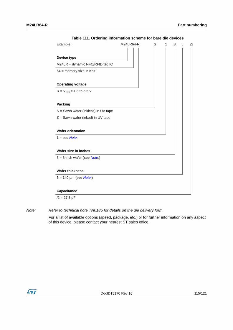
DocID15170 Rev 16 115/121
M24LR64-R Part numbering
Note: Refer to technical note TN0185 for details on the die delivery form.
For a list of available options (speed, package, etc.) or for further information on any aspect of this device, please contact your nearest ST sales office.
Table 111. Ordering information scheme for bare die devices
Example: M24LR64-R S 1 8 5 /2
Device type
M24LR = dynamic NFC/RFID tag IC
64 = memory size in Kbit
Operating voltage
R = VCC = 1.8 to 5.5 V
Packing
S = Sawn wafer (inkless) in UV tape
Z = Sawn wafer (inked) in UV tape
Wafer orientation
1 = see Note:
Wafer size in inches
8 = 8-inch wafer (see Note:)
Wafer thickness
5 = 140 µm (see Note:)
Capacitance
/2 = 27.5 pF
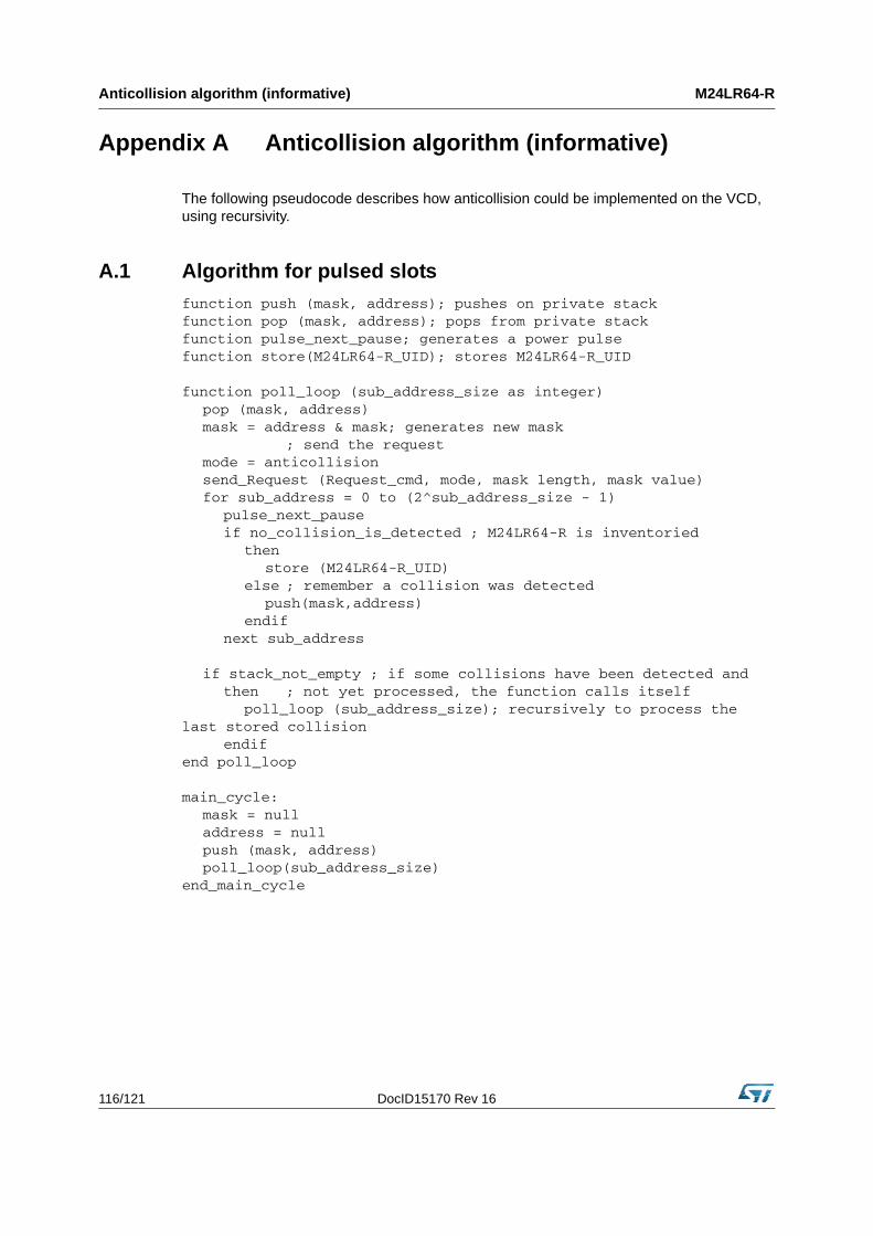
Anticollision algorithm (informative) M24LR64-R
116/121 DocID15170 Rev 16
Appendix A Anticollision algorithm (informative)
The following pseudocode describes how anticollision could be implemented on the VCD, using recursivity.
A.1 Algorithm for pulsed slots
function push (mask, address); pushes on private stackfunction pop (mask, address); pops from private stackfunction pulse_next_pause; generates a power pulsefunction store(M24LR64-R_UID); stores M24LR64-R_UID
function poll_loop (sub_address_size as integer)pop (mask, address)mask = address & mask; generates new mask
; send the requestmode = anticollisionsend_Request (Request_cmd, mode, mask length, mask value)for sub_address = 0 to (2^sub_address_size - 1)
pulse_next_pauseif no_collision_is_detected ; M24LR64-R is inventoried
thenstore (M24LR64-R_UID)
else ; remember a collision was detected push(mask,address)
endifnext sub_address
if stack_not_empty ; if some collisions have been detected andthen ; not yet processed, the function calls itself
poll_loop (sub_address_size); recursively to process the last stored collision
endifend poll_loop
main_cycle:mask = nulladdress = nullpush (mask, address)poll_loop(sub_address_size)
end_main_cycle
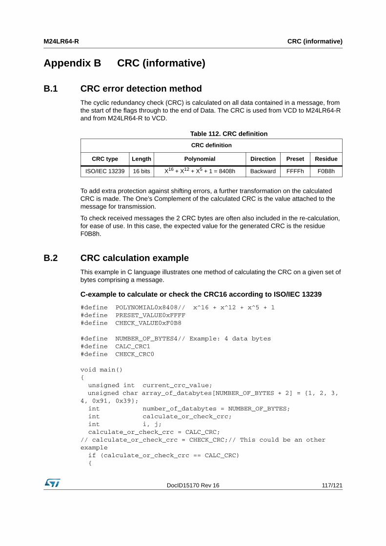
DocID15170 Rev 16 117/121
M24LR64-R CRC (informative)
Appendix B CRC (informative)
B.1 CRC error detection method
The cyclic redundancy check (CRC) is calculated on all data contained in a message, from the start of the flags through to the end of Data. The CRC is used from VCD to M24LR64-R and from M24LR64-R to VCD.
To add extra protection against shifting errors, a further transformation on the calculated CRC is made. The One’s Complement of the calculated CRC is the value attached to the message for transmission.
To check received messages the 2 CRC bytes are often also included in the re-calculation, for ease of use. In this case, the expected value for the generated CRC is the residue F0B8h.
B.2 CRC calculation example
This example in C language illustrates one method of calculating the CRC on a given set of bytes comprising a message.
C-example to calculate or check the CRC16 according to ISO/IEC 13239
#define POLYNOMIAL0x8408// x^16 + x^12 + x^5 + 1#define PRESET_VALUE0xFFFF#define CHECK_VALUE0xF0B8
#define NUMBER_OF_BYTES4// Example: 4 data bytes#define CALC_CRC1#define CHECK_CRC0
void main(){ unsigned int current_crc_value; unsigned char array_of_databytes[NUMBER_OF_BYTES + 2] = {1, 2, 3, 4, 0x91, 0x39}; int number_of_databytes = NUMBER_OF_BYTES; int calculate_or_check_crc; int i, j; calculate_or_check_crc = CALC_CRC;// calculate_or_check_crc = CHECK_CRC;// This could be an other example if (calculate_or_check_crc == CALC_CRC) {
Table 112. CRC definition
CRC definition
CRC type Length Polynomial Direction Preset Residue
ISO/IEC 13239 16 bits X16 + X12 + X5 + 1 = 8408h Backward FFFFh F0B8h
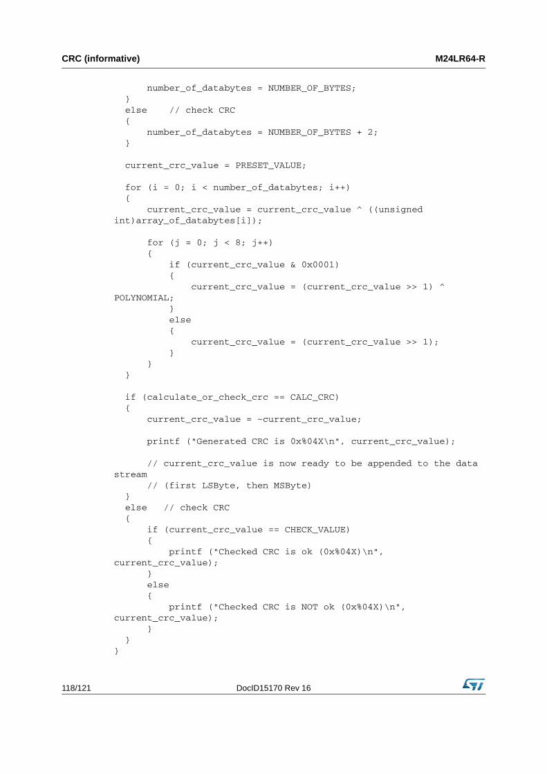
CRC (informative) M24LR64-R
118/121 DocID15170 Rev 16
number_of_databytes = NUMBER_OF_BYTES; } else // check CRC { number_of_databytes = NUMBER_OF_BYTES + 2; }
current_crc_value = PRESET_VALUE;
for (i = 0; i < number_of_databytes; i++) { current_crc_value = current_crc_value ^ ((unsigned int)array_of_databytes[i]);
for (j = 0; j < 8; j++) { if (current_crc_value & 0x0001) { current_crc_value = (current_crc_value >> 1) ^ POLYNOMIAL; } else { current_crc_value = (current_crc_value >> 1); } } }
if (calculate_or_check_crc == CALC_CRC) { current_crc_value = ~current_crc_value;
printf ("Generated CRC is 0x%04X\n", current_crc_value);
// current_crc_value is now ready to be appended to the data stream // (first LSByte, then MSByte) } else // check CRC { if (current_crc_value == CHECK_VALUE) { printf ("Checked CRC is ok (0x%04X)\n", current_crc_value); } else { printf ("Checked CRC is NOT ok (0x%04X)\n", current_crc_value); } }}
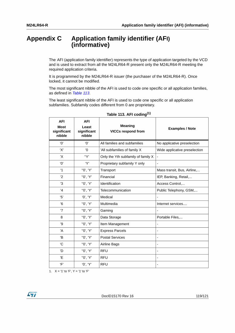
DocID15170 Rev 16 119/121
M24LR64-R Application family identifier (AFI) (informative)
Appendix C Application family identifier (AFI) (informative)
The AFI (application family identifier) represents the type of application targeted by the VCD and is used to extract from all the M24LR64-R present only the M24LR64-R meeting the required application criteria.
It is programmed by the M24LR64-R issuer (the purchaser of the M24LR64-R). Once locked, it cannot be modified.
The most significant nibble of the AFI is used to code one specific or all application families, as defined in Table 113.
The least significant nibble of the AFI is used to code one specific or all application subfamilies. Subfamily codes different from 0 are proprietary.
Table 113. AFI coding(1)
1. X = '1' to 'F', Y = '1' to 'F'
AFI
Most significant
nibble
AFI
Least significant
nibble
Meaning
VICCs respond fromExamples / Note
‘0’ ‘0’ All families and subfamilies No applicative preselection
‘X’ '0 'All subfamilies of family X Wide applicative preselection
'X '‘Y’ Only the Yth subfamily of family X -
‘0’ ‘Y’ Proprietary subfamily Y only -
‘1 '‘0’, ‘Y’ Transport Mass transit, Bus, Airline,...
'2 '‘0’, ‘Y’ Financial IEP, Banking, Retail,...
'3 '‘0’, ‘Y’ Identification Access Control,...
'4 '‘0’, ‘Y’ Telecommunication Public Telephony, GSM,...
‘5’ ‘0’, ‘Y’ Medical -
'6 '‘0’, ‘Y’ Multimedia Internet services....
'7 '‘0’, ‘Y’ Gaming -
8 '‘0’, ‘Y’ Data Storage Portable Files,...
'9 '‘0’, ‘Y’ Item Management -
'A '‘0’, ‘Y’ Express Parcels -
'B '‘0’, ‘Y’ Postal Services -
'C '‘0’, ‘Y’ Airline Bags -
'D '‘0’, ‘Y’ RFU -
'E '‘0’, ‘Y’ RFU -
‘F’ ‘0’, ‘Y’ RFU -

Revision history M24LR64-R
120/121 DocID15170 Rev 16
Revision history
.
Table 114. Document revision history
Date Revision Changes
24-Jun-2010 10
Added 8” wafer delivery form and update endurance on cover page.
Updated VCC overview and replaced diode by regulator in Section 2.6: Supply voltage (VCC).
Removed RF address column from Table 6: Sector Security Status Byte area and Table 14: System parameter sector.
Updated hSTG in Table 99: Absolute maximum ratings.
Added Table 111: Ordering information scheme for bare die devices.
09-Aug-2010 11Updated Table 111: Ordering information scheme for bare die devices.
02-Dec-2010 12
Updated ISO references under Features.
Updated Section 2.4: Antenna coil (AC0, AC1), Table 99: Absolute maximum ratings and Table 105: RF characteristics.
Renamed Section 29 and Table 105.
Deleted Table 106 RF DC Characteristics.
27-Oct-2011 13 Updated footnote (2) of Table 105: RF characteristics.
05-Jan-2012 14 Modified Table 10: Password system area on page 24.
13-Jun-2013 15Added “Dynamic NFC/RFID tag IC” to the title, Section 1: Description, and the M24LR definition in Table 110 and Table 111.
25-Jul-2013 16
Replaced UFDFPN8 (MB) drawing by UFDFPN8 (MC) drawing on page 1.
Added MC drawing to Figure 75: UFDFPN8 (MLP8) – Ultra thin fine pitch dual flat package no lead 2 x 3 mm, package outline.
Added “D2 (MC)” and “E2 (MC)” rows to Table 108: UFDFPN8 (MLP8) – Ultra thin fine pitch dual flat package no lead 2 x 3 mm, package mechanical data.

DocID15170 Rev 16 121/121
M24LR64-R
Please Read Carefully:
Information in this document is provided solely in connection with ST products. STMicroelectronics NV and its subsidiaries (“ST”) reserve theright to make changes, corrections, modifications or improvements, to this document, and the products and services described herein at anytime, without notice.
All ST products are sold pursuant to ST’s terms and conditions of sale.
Purchasers are solely responsible for the choice, selection and use of the ST products and services described herein, and ST assumes noliability whatsoever relating to the choice, selection or use of the ST products and services described herein.
No license, express or implied, by estoppel or otherwise, to any intellectual property rights is granted under this document. If any part of thisdocument refers to any third party products or services it shall not be deemed a license grant by ST for the use of such third party productsor services, or any intellectual property contained therein or considered as a warranty covering the use in any manner whatsoever of suchthird party products or services or any intellectual property contained therein.
UNLESS OTHERWISE SET FORTH IN ST’S TERMS AND CONDITIONS OF SALE ST DISCLAIMS ANY EXPRESS OR IMPLIEDWARRANTY WITH RESPECT TO THE USE AND/OR SALE OF ST PRODUCTS INCLUDING WITHOUT LIMITATION IMPLIEDWARRANTIES OF MERCHANTABILITY, FITNESS FOR A PARTICULAR PURPOSE (AND THEIR EQUIVALENTS UNDER THE LAWSOF ANY JURISDICTION), OR INFRINGEMENT OF ANY PATENT, COPYRIGHT OR OTHER INTELLECTUAL PROPERTY RIGHT.
ST PRODUCTS ARE NOT AUTHORIZED FOR USE IN WEAPONS. NOR ARE ST PRODUCTS DESIGNED OR AUTHORIZED FOR USEIN: (A) SAFETY CRITICAL APPLICATIONS SUCH AS LIFE SUPPORTING, ACTIVE IMPLANTED DEVICES OR SYSTEMS WITHPRODUCT FUNCTIONAL SAFETY REQUIREMENTS; (B) AERONAUTIC APPLICATIONS; (C) AUTOMOTIVE APPLICATIONS ORENVIRONMENTS, AND/OR (D) AEROSPACE APPLICATIONS OR ENVIRONMENTS. WHERE ST PRODUCTS ARE NOT DESIGNEDFOR SUCH USE, THE PURCHASER SHALL USE PRODUCTS AT PURCHASER’S SOLE RISK, EVEN IF ST HAS BEEN INFORMED INWRITING OF SUCH USAGE, UNLESS A PRODUCT IS EXPRESSLY DESIGNATED BY ST AS BEING INTENDED FOR “AUTOMOTIVE,AUTOMOTIVE SAFETY OR MEDICAL” INDUSTRY DOMAINS ACCORDING TO ST PRODUCT DESIGN SPECIFICATIONS.PRODUCTS FORMALLY ESCC, QML OR JAN QUALIFIED ARE DEEMED SUITABLE FOR USE IN AEROSPACE BY THECORRESPONDING GOVERNMENTAL AGENCY.
Resale of ST products with provisions different from the statements and/or technical features set forth in this document shall immediately voidany warranty granted by ST for the ST product or service described herein and shall not create or extend in any manner whatsoever, anyliability of ST.
ST and the ST logo are trademarks or registered trademarks of ST in various countries.Information in this document supersedes and replaces all information previously supplied.
The ST logo is a registered trademark of STMicroelectronics. All other names are the property of their respective owners.
© 2013 STMicroelectronics - All rights reserved
STMicroelectronics group of companies
Australia - Belgium - Brazil - Canada - China - Czech Republic - Finland - France - Germany - Hong Kong - India - Israel - Italy - Japan - Malaysia - Malta - Morocco - Philippines - Singapore - Spain - Sweden - Switzerland - United Kingdom - United States of America
www.st.com