Embed Size (px)
Citation preview

Dynamic Response of a-InGaZnO Thin-Film Transistors for Ultra-High Definition Active-Matrix Liquid Crystal Displays
Eric K.-H. Yu, Rui Zhang, Linsen Bie, Alex Kuo, and Jerzy Kanicki* Department of Electrical Engineering and Computer Science, Displays and Detectors Laboratory
University of Michigan Ann Arbor, Michigan 48105, United States
*Corresponding author: [email protected]
Abstract: The dynamic response of amorphous In-Ga-Zn-O (a-IGZO) thin-film transistors (TFTs) are compared with hydrogenated amorphous silicon (a-Si:H) TFTs. We study the storage capacitor (Cst) charging characteristics by applying gate and data voltage waveforms for ultra-high definition (UHD) active-matrix flat-panel displays (AM-FPDs). Experimental data show that the charging characteristics of a-Si:H TFTs is clearly inadequate for UHD AM-FPDs and that a-IGZO TFTs are at least capable of supporting up to 8K×4K resolution at 480 Hz. The impact of the gate voltage falling edge on feedthrough voltage (ΔVP) is investigated in detail. Although for the same Cst the ΔVP is larger for a-IGZO TFT than a-Si:H TFTs, Cst of the a-IGZO TFT can be made larger to reduce ΔVP without obvious degradations in charging behavior. Gate overdrive operation is also demonstrated for a-IGZO TFTs to improve charging characteristics without visible impact on ΔVP. Our results show that the a-IGZO TFT is a suitable technology for next-generation UHD high-frame rate AM-FPDs.
Keywords: AM-FPD; active-matrix; flat-panel displays; thin-film transistors; AM-LCD; dynamic response; amorphous silicon; feedthrough voltage; a-IGZO; timing; falling edge; overdrive
Introduction Next generation ultra-high definition (UHD) displays have resolutions of 4K×2K (3840×2160 pixels) or 8K×4K (7680×4320 pixels) and support frame rates of up to 120 Hz [1]. For 3D displays or motion blur reduction by image interpolation, frame rates of 240 Hz or higher are needed [2]. Improvements to display resolution and frame rate both correspond to shorter time margin available for each pixel to complete charging, thus placing stringent requirements on the dynamic response of thin-film transistor (TFT) backplane technology for active-matrix liquid crystal displays (AM-LCDs) and active-matrix organic light-emitting diodes (AM-OLEDs). The dynamic response of the hydrogenated amorphous silicon (a-Si:H) TFT pixel electrode has been studied extensively in literature. The feedthrough voltage (ΔVP), which results from gate-source overlap capacitance (CGS) and channel charge redistribution, is the main source of image flickering in AM-LCD operation and a key metric in TFT dynamic response [3]. Takabatake et al. reported a robust analytical model for ΔVP that is very consistent with
experimental values [4]. Kitazawa et al. investigated the impact of a-Si:H TFT device structural differences on ΔVP [5]. Aoki conducted a comprehensive study detailing an analytical model of a-Si:H TFT dynamic operation with the liquid-crystal cell capacitance included, and the model is verified by experimental data [6]. Lee et al. studied the dynamic response of a-Si:H TFT for AM-OLED pixel electrode, and reported in detail ΔVP and charging time (tCH) for various TFT structures and waveform parameters [7]. The amorphous In-Ga-Zn-O (a-IGZO) TFT, because of its superior field-effect mobility (µFE) on the order of 10 cm2/Vs and good electrical stability, has emerged as a leading candidate for next-generation active-matrix flat-panel display (AM-FPD) backplane technology [8]. Our group has previously described preliminary results on the dynamic response of a-IGZO TFT pixel electrodes in terms of its storage capacitance (Cst) and TFT dimension dependences [9]. Initial data suggest that a-IGZO TFT showed very favorable dynamic characteristics when operated at a very high frequency. To date, however, there are still no comprehensive reports of a-IGZO TFT dynamic response published in peer-reviewed journal literature. In this work, our objective is to evaluate and compare the dynamic response of a-Si:H and a-IGZO TFT in the context of pixel electrodes for UHD AM-FPDs. For all TFTs fabricated, charging characteristics are investigated for various gate waveform specifications. The equations governing ΔVP are thoroughly analyzed and the impact of the gate signal falling edge, gate voltage, and data voltage are studied in detail. The ΔVP as calculated from equation are used to verify the experimental values of ΔVP and its relationship with Cst. We also report the gate waveform overdrive operation of a-IGZO TFTs, which is expected to improve the dynamic response of a-IGZO TFT pixel electrodes with no drawbacks.
Experiment The fabrication of the BCE-type bottom-gate a-Si:H TFT follows the process described by Kuo et al. [10] and is briefly described here. The a-Si:H TFT has patterned chromium gate (200 nm) followed by two bilayers of amorphous silicon nitride (a-SiNx:H, 400 nm) and a-Si:H (170 nm), both deposited by PECVD. The interfacial a-SiNx:H and a-Si:H layers of the two bilayers are

deposited at lower deposition rates than the outer layers, and thus the channel-insulator interface region is of higher density and superior electronic property. A 70-nm layer of phosphorous-doped n+ a-Si:H is also deposited by PECVD to act as S/D contact regions. The active island is dry-etched using an SF6:Cl2:O2:He gaseous mixture. The S/D electrodes are 200 nm of sputtered molybdenum (Mo) and are defined by wet etching with a phosphorous-nitric-acetic acid mixture. The resulting gate-S/D metal electrode overlap (OVLP) is 3 µm. During the S/D electrode definition, one set of TFTs (recessed TFTs) is intentionally over-etched for 160 s such that the Mo is also etched laterally, causing OVLP to be reduced to 2 µm (recess length dREC = 1 µm). Lastly, we dry-etched (HBr:Cl2) the n+ a-S i:H and 70 nm of a-Si:H in the channel region. The a-Si:H TFT dimensions are width (W)/length (L) = 57.5 µm/7.5 µm. The patterned photoresist remained on top of the Mo electrodes throughout the S/D definition steps and is removed at the end. We can approximate the gate-source capacitance in the area of overlap between the source and gate electrodes using the equation:
!!" = !×!"#$× !!"!! + !!"#!! !!, (1)
where CGI is the gate insulator capacitance and Cact is the active layer (a-Si:H) capacitance. Using (1), we calculate CGS = 0.021 pF for normal TFTs and 0.014 pF for recessed S/D TFTs. The storage capacitor of Cst = 0.19 pF is fabricated at the same time as the TFT using the gate insulator layer as dielectric (400 nm) and is connected in series to the TFT source terminal for the dynamic response test circuit. The a-Si:H TFT top-view micrograph and cross-section SEM images and diagrams illustrating the recess are shown in Fig. 1. To fabricate the a-IGZO TFT, 100 nm of Mo is first deposited on a glass substrate (Corning Eagle or Asahi PD-200) using sputtering and then defined using dry etching. The gate insulator is 200 nm of PECVD amorphous silicon oxide (a-SiOx) deposited at 380 °C. The channel layer (50 nm) is then deposited by dc-sputtering an a-IGZO target of composition In:Ga:Zn:O = 2:2:1:7. The a-IGZO active islands are defined using dilute oxalic acid (0.05 M) and then annealed in ambient air at 300 °C for 30 minutes on a hot plate. The gate vias are then opened using dry etching and subsequently 100 nm of Mo is sputtered during metallization. The S/D electrodes are defined using wet etching with 30% H2O2. The dimensions of the a-IGZO TFTs fabricated are W/L =
Figure. 1. (a) Top-view micrograph and (b) SEM image and cross-section diagram of the bottom-gate a-Si:H TFT used in this study. The SEM image and cross-section diagram of the a-Si:H TFT with the S/D-recess is
shown in (c), where the recess length (dREC) is 1 µm.
Figure. 2. (a) Top-view micrograph and (b) cross-sectional diagrams and SEM images of the bottom-gate a-IGZO TFT used in this study.

74 µm/3 µm and OVLP = 5 µm. Using (1), we estimate CGS = 0.06 pF for the a-IGZO TFTs. After device processing, the TFTs undergo one final annealing step of 300°C for 30 minutes. For the dynamic response test circuit, a storage capacitor is fabricated in series with the a-IGZO TFT source terminal. To investigate the impact of storage capacitance, test circuits with Cst = 0.29 pF, 0.65 pF, and 1.15 pF are evaluated in this study. The top-view micrograph and cross-section diagram of the a-IGZO TFT are shown in Fig. 2. The set-up for evaluating the dynamic response of a-Si:H and a-IGZO TFTs is as follows: a two-channel HP 8110A pulse generator is connected to the drain and gate electrodes of the test circuit, where the drain is the data signal and the gate is the select signal. A low-input capacitance (0.02 pF) and high-impedance (input leakage < 10 fA) Picoprobe (HP18C-1-5-HV, GGB Industries) is used to measure the voltage of the storage capacitor Cst at the TFT source terminal. An Agilent MSO7104B oscilloscope is used to record the storage capacitor
voltage measured by the Picoprobe with respect to time. Figure 3(a) shows the schematic for the set-up used in this study. The waveforms applied to the gate and data lines are shown in Figs. 3(b) and 3(c) respectively. For each frame, two gate pulses of VGH = 18 V are applied to the TFT gate electrode – one for set and another for reset. The low voltage of the gate waveform is VGL = −2V. The gate pulse width, indicated in Fig. 3(b) as the charging-time margin (tcm), is the time available to charge/discharge Cst (for set/reset) in each pixel when the row lines are selected in AM-FPD operation. For a simple driving scheme without any charge sharing or pre-charging, tcm is defined as [11]:
!!" = !Frame Rate × Number of Row Lines
(2)
In this study, we are most interested in the charging-time margins corresponding to UHD AM-FPD resolutions and frame rates in [1]. Using (2), the tcm are calculated based on these specifications and summarized in Table I. For
Figure 3. (a) The schematic for the set-up used to evaluate the dynamic response of the one-TFT-one-capacitor test circuit. (b) The gate voltage applied is VGH = 18 V when charging/discharging and VGL = −2 V at all other times. The charging-time margin tcm is
the time available for the storage capacitor to completely charge/discharge. (c) The data voltage
applied is VDH = 10 V for set and VDL = 0 V for reset. The set/reset duration is 3×tcm. The falling edge of
the waveforms is 10 ns except where specified.
Table 1. The calculated charging-time margins based on AM-FPD resolution and frame rate
specifications Resolution
Frame Rate
Full HD (1920×1080)
4K UHD (3840×2160)
8K UHD (7680×4320)
60 Hz 15.4 µs (16 µs) 7.7 µs (8 µs) 3.9 µs (4 µs) 120 Hz 7.7 µs (8 µs) 3.9 µs (4 µs) 1.9 µs (2 µs)
240 Hz 3.9 µs (4 µs) 1.9 µs (2 µs) 0.96 µs (1 µs)
480 Hz 1.9 µs (2 µs) 0.96 µs (1 µs) 0.48 µs (0.5 µs)
Figure. 4. The output voltage measured at the source terminal of the a-Si:H or a-IGZO TFTs with
the data and gate waveform applied. The feedthrough voltage ΔVP is the output voltage drop
at the end of tcm after the gate voltage is flipped from VGH to VGL.

each frame, a single fixed pulse of data voltage VDH = 10 V is applied to the drain terminal for set, after which the data voltage is returned to its low level VDL = 0 V for reset. For the data voltage waveform, each set/reset period is defined to be 3×tcm. Each gate pulse arrives exactly 1×tcm after the data voltage is applied/removed. The rising and falling edge time (tFE) of the data and gate pulses are all 10 ns unless where specified. For falling edge values other than 10 ns, the corresponding rising edge is always 10% of that.
Results and Discussion
Charging Characteristics of a-Si:H and a-IGZO TFTs for Ultra-High Definition AM-FPDs The output voltage (Vout) at the source terminal of the a -Si:H or a-IGZO TFT as a function of time after applying the gate and data waveforms is shown in Fig. 4. In this figure, the gate and data waveforms are based on tcm = 16 µs, which corresponds to Full HD 1080p resolution at 60 Hz – the current mainstream AM-LCD specification. In TFT pixel circuit dynamic response, one of the most important metrics is the storage capacitance charging behavior: incomplete charging directly causes the display gray-scale to deteriorate. In the figure, both a-Si:H TFTs
are able to charge completely to VDH = 10 V within 16 µs, but the RC exponential charging curvature is clearly observable in the time-scale of the figure. In contrast, Cst charging by the a-IGZO TFT appears almost instantaneous. From the figure, we can extract the charging time constant (τ) at Vout = 6.3 V (0.63 VDH) for each device structure. The values of τ are 1.35 µs, 0.76 µs, and 0.08 µs for normal a-Si:H, recessed S/D a-Si:H, and a-IGZO TFT, respectively. The fact that the charging time constant of a-IGZO TFT is at least an order of magnitude lower than that of any a-Si:H TFT is mainly due to the much higher µFE of a-IGZO. The charging behavior can be modeled by a simple RC model, in which the TFT drain current (ID) supplies the charges to the capacitor:
!!" !!!"#!" = !!. (3)
We can approximate ID using the following simplified ideal MOSFET equation, which is appropriate for small drain-source voltages:
!! = !!"!!" !! !! − !!"# − !!! (!! − !!"#). (4)
The µFE in (4) represents the TFT field-effect mobility. Combining (3) and (4), and solving for time, the elapsed
Figure 5. The output voltage at the source terminal of the a-Si:H and a-IGZO TFTs after applying the gate and data voltage waveforms based on (a) tcm = 16 µs, (b) tcm = 8 µs, (c) tcm = 4 µs, (d) tcm = 2 µs, corresponding to the
AM-FPD specifications in Table I. Cst is 1.15 pF for a-IGZO TFTs and 0.19 pF for a-Si:H TFTs.

time for charging Cst to a specific voltage VS can be derived [7]:
!!! = !!"!!!"!!"!
!(!!"!!!"!!!!)
ln !!"!!!"#!!!! !!"(!!"!!!!)(!!"!!!"#)
. (5)
Within the context of this study, we note from (5) that tch is directly proportional to Cst and inversely proportional to both W/L and µFE. Considering that µFE of a-IGZO is 1–2 orders of magnitude larger than a-Si:H, the fact that tch of a-IGZO TFT is much smaller than a-Si:H TFT is within our expectations, even though the a-IGZO TFT test circuit has a much larger Cst. To highlight the advantage of a-IGZO TFT over a-Si:H TFT in terms of charging characteristics, we apply gate and data waveforms based on the charging-time margins in Table I, and show the resulting output voltages in Fig. 5 and Fig. 6. In Fig. 5(a), where tcm = 16 µs, the a-Si:H TFTs are capable of fully charging Cst within the allotted time. As tcm is reduced to 8 µs and 4 µs in Figs. 5(b) and 5(c), the a-Si:H TFTs begin to struggle to charge the storage capacitor. In Fig. 5(d), where tcm = 2 µs represents the 8K×4K UHD AM-FPD at 120 Hz, the a-Si:H TFTs can only charge Cst to 7.2 V (normal) and 8.7 V (recessed S/D). In real-world AM-LCD operation, gate and data bus-line RC delay may impose additional requirements for the charging-time margin [12], meaning that further degradations are expected for a-Si:H TFTs. In comparison, the simple BCE-type bottom-gate a-IGZO TFT is able to readily charge Cst to VDH = 10 V with ease for all four cases shown in Fig. 5. Charging behavior of the a-IGZO TFT pixel electrode is shown in Fig. 6 for (a) tcm = 1 µs and (b) 0.5 µs, corresponding to 8K×4K resolution at 240 and 480 Hz, and the Cst is fully charged
to VDH before the end of tcm.
Feedthrough Voltage of a-Si:H and a-IGZO TFTs The feedthrough voltage (ΔVP) indicated in Fig. 4 is the voltage drop at the TFT source terminal after the gate voltage flips from VGH to VGL. It was originally observed as clock feedthrough in CMOS switched-capacitor circuits, affecting its high-frequency accuracy [13]. In AM-FPD operation, ΔVP of the pixel electrode primarily manifests itself as image flickering [3]. The two primary contributions to ΔVP are capacitance feedthrough from CGS to Cst and channel charge redistribution. Takabatake et al. developed a series of equations describing ΔVP, which we briefly summarize in the following discussion [4]. The capacitance feedthrough component of ΔVP can be calculated from:
!!!,! = !!"!!"!!!"
(!!! + !!" − !!"). (6)
In (6), capacitance feedthrough is dependent on the ratio between CGS and Cst. Overlap capacitance can be completely eliminated through the use of a self-aligned structure [14–17], but is difficult to avoid in the commonly used bottom-gate structure such as the ones in this study. Channel charge redistribution occurs when the TFT switches to its OFF-state and the accumulated channel charge (Qch) has to be released. We can estimate Qch in the area of overlap (A) between the gate electrode and the active layer with the equation:
!!! = !!"! !!" − !!! − !!" . (7)
In our TFTs, we calculate the overlap area as A = W×(L+2OVLP). When the gate signals falls abruptly from VGH to Vth + VDH, the TFT is turned off and any Qch in the channel is redistributed onto Cst:
!!!,!" = ! !!!!!"
= ! !!"! !!"!!!!!!!!!!"
, (8)
where f is a constant factor related to the gate falling edge. The total ΔVP is a sum of the (6) and (8) [4]:
!!! = !!!,! + !!!,!" = !!"!!"!!!"
!!! + !!" − !!" +! !!"! !!"!!!!!!!"
!!". (9)
The upper limit for f is exactly 0.5, for which the TFT is turned off so abruptly that no charges can be released through the drain terminal while VG is reduced from VGH to Vth + VDH. In this upper limit, the gate voltage falling edge (tFE) satisfies the condition:
!!" ≪ !!!!"⋅!!!,!"
. (10)
The right-hand side of (10) is the channel transit time for accumulated charges. For tFE below this upper limit, f decreases monotonically until it approaches the lower
Figure 6. The output voltage at the source terminal of the a-IGZO TFTs after applying the gate and data voltage waveforms based on (a) tcm = 1 µs and (b) tcm = 0.5 µs corresponding to 8K×4K resolution at
240 and 480 Hz. For this figure, Cst = 1.15 pF.

limit of f = 0. In this lower limit, tFE is much slower than channel transit time of the charge carriers:
!!" ≫ !!!!"⋅!!!,!"
. (11)
In this case, most if not all of Qch can be released through the drain terminal while VG is reduced from VGH and Vth + VDH. Contribution from (8) becomes negligible (f ≈ 0) and the total feedthrough voltage is simply:
!!! = !!!,! = !!"!!"!!!"
(!!! + !!" − !!") (12)
We note that according (12), ΔVP does not depend on VGH for slow tFE. We can experimentally verify this by
comparing the VGH dependence of ΔVP for slow and fast tFE. The output voltage of the a-IGZO TFT test circuit is shown in Fig. 7, where the falling edge of the gate pulse is (a) tFE = 10 ns and (b) tFE = 10 µs. In Fig. 7(c), ΔVP corresponding to different VGH are extracted for tFE = 10 µs, 1 µs, and 10 ns. Only VGH ≥ 10.3 V (Vth + VDH) are shown in the figure, below which the TFT is in the off region and the equation has no meaning. We first calculate the ΔVP for various VGH using (9) with f = 0.5 and we find that the generated values are much larger than the experimental data for tFE = 10 ns. This means that the actual fast-tFE limit for a-IGZO TFTs is much smaller than
Figure 7. The output voltage of the a-IGZO TFT test circuit for waveforms with VGH varied from 18 V to 12 V for (a) tFE = 10 ns and (b) tFE = 10 µs. The storage
capacitance tested in this figure is 0.29 pF. In (c), the ΔVP extracted for tFE = 10 ns (empty squares), 1 µs (solid circles), and 10 µs (asterisks) are shown. The calculated ΔVP values are also shown in the figure
for f = 0 to 0.5.
Figure 8. The output voltage of the a-IGZO and a-Si:H TFT test circuit for waveforms with tFE varied
from 10 ns to 10 µs for (a) a-Si:H (normal) and (b) a-IGZO TFTs. The storage capacitance tested in this figure is 0.19 pF and 0.29 pF for the a-IGZO and a-Si:H TFTs, respectively. The ΔVP are extracted from
(a) and (b) and shown in (c). The ΔVP for the recessed S/D a-Si:H TFT is also shown in (c). Using
(10), the channel transit time is calculated and denoted (c) as dashed line and dotted line for a-
IGZO and a-Si:H TFTs.
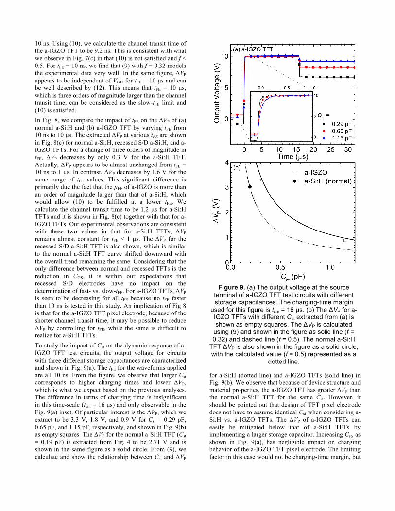
10 ns. Using (10), we calculate the channel transit time of the a-IGZO TFT to be 9.2 ns. This is consistent with what we observe in Fig. 7(c) in that (10) is not satisfied and f < 0.5. For tFE = 10 ns, we find that (9) with f = 0.32 models the experimental data very well. In the same figure, ΔVP appears to be independent of VGH for tFE = 10 µs and can be well described by (12). This means that tFE = 10 µs, which is three orders of magnitude larger than the channel transit time, can be considered as the slow-tFE limit and (10) is satisfied. In Fig. 8, we compare the impact of tFE on the ΔVP of (a) normal a-Si:H and (b) a-IGZO TFT by varying tFE from 10 ns to 10 µs. The extracted ΔVP at various tFE are shown in Fig. 8(c) for normal a-Si:H, recessed S/D a-Si:H, and a-IGZO TFTs. For a change of three orders of magnitude in tFE, ΔVP decreases by only 0.3 V for the a-Si:H TFT. Actually, ΔVP appears to be almost unchanged from tFE = 10 ns to 1 µs. In contrast, ΔVP decreases by 1.6 V for the same range of tFE values. This significant difference is primarily due the fact that the µFE of a-IGZO is more than an order of magnitude larger than that of a-Si:H, which would allow (10) to be fulfilled at a lower tFE. We calculate the channel transit time to be 1.2 µs for a-Si:H TFTs and it is shown in Fig. 8(c) together with that for a-IGZO TFTs. Our experimental observations are consistent with these two values in that for a-Si:H TFTs, ΔVP remains almost constant for tFE < 1 µs. The ΔVP for the recessed S/D a-Si:H TFT is also shown, which is similar to the normal a-Si:H TFT curve shifted downward with the overall trend remaining the same. Considering that the only difference between normal and recessed TFTs is the reduction in CGS, it is within our expectations that recessed S/D electrodes have no impact on the determination of fast- vs. slow-tFE. For a-IGZO TFTs, ΔVP is seen to be decreasing for all tFE because no tFE faster than 10 ns is tested in this study. An implication of Fig 8 is that for the a-IGZO TFT pixel electrode, because of the shorter channel transit time, it may be possible to reduce ΔVP by controlling for tFE, while the same is difficult to realize for a-Si:H TFTs. To study the impact of Cst on the dynamic response of a-IGZO TFT test circuits, the output voltage for circuits with three different storage capacitances are characterized and shown in Fig. 9(a). The tFE for the waveforms applied are all 10 ns. From the figure, we observe that larger Cst corresponds to higher charging times and lower ΔVP, which is what we expect based on the previous analyses. The difference in terms of charging time is insignificant in this time-scale (tcm = 16 µs) and only observable in the Fig. 9(a) inset. Of particular interest is the ΔVP, which we extract to be 3.3 V, 1.8 V, and 0.9 V for Cst = 0.29 pF, 0.65 pF, and 1.15 pF, respectively, and shown in Fig. 9(b) as empty squares. The ΔVP for the normal a-Si:H TFT (Cst = 0.19 pF) is extracted from Fig. 4 to be 2.71 V and is shown in the same figure as a solid circle. From (9), we calculate and show the relationship between Cst and ΔVP
for a-Si:H (dotted line) and a-IGZO TFTs (solid line) in Fig. 9(b). We observe that because of device structure and material properties, the a-IGZO TFT has greater ΔVP than the normal a-Si:H TFT for the same Cst. However, it should be pointed out that design of TFT pixel electrode does not have to assume identical Cst when considering a-Si:H vs. a-IGZO TFTs. The ΔVP of a-IGZO TFTs can easily be mitigated below that of a-Si:H TFTs by implementing a larger storage capacitor. Increasing Cst, as shown in Fig. 9(a), has negligible impact on charging behavior of the a-IGZO TFT pixel electrode. The limiting factor in this case would not be charging-time margin, but
Figure 9. (a) The output voltage at the source terminal of a-IGZO TFT test circuits with different storage capacitances. The charging-time margin
used for this figure is tcm = 16 µs. (b) The ΔVP for a-IGZO TFTs with different Cst extracted from (a) is shown as empty squares. The ΔVP is calculated
using (9) and shown in the figure as solid line (f = 0.32) and dashed line (f = 0.5). The normal a-Si:H
TFT ΔVP is also shown in the figure as a solid circle, with the calculated value (f = 0.5) represented as a
dotted line.

rather the aperture ratio of the AM-LCD pixel. This also bodes well for a-IGZO TFTs as the backplane technology of large-area AM-LCDs, which have larger liquid-crystal cells and thus greater cell capacitance. For the recessed S/D a-Si:H TFT, ΔVP is extracted from Fig. 4 to be 2.71 V. Since the S/D-recess improves ΔVP without inducing any degradations in charging characteristics, it should be a useful technique in a-Si:H TFT fabrication. We note that the discrepancy between experimental and calculated values is much larger in this case, where 2.33 V is calculated from (9) assuming OVLP = 2 µm. Although the metal S/D electrodes are recessed by 1/3, the n+ a-Si:H S/D contact regions remain unmodified. This makes simple areal estimation of CGS appropriate only for normal bottom-gate TFT structure without recess. Now that the model described by (9) has been verified by experimental data for a-IGZO and a-Si:H TFTs, we can also use it to explore some other parameters that may potentially impact TFT pixel electrode operation in AM-FPDs. We note that (9) is dependent on VDH for both high- or low-tFE limits because VDH contributes to both capacitance feedthrough and charge redistribution. During AM-FPD operation, column drivers apply the various data voltage to the TFT drain terminal to program the pixel. Therefore, it is informative to explore the relationship between VDH and ΔVP. We fix VGH = 18 V and Cst = 0.29 pF for a-IGZO and 0.19 pF for a-Si:H TFTs. The ΔVP is calculated for VDH from 0 V to 10 V and shown in Fig. 10 (a) for a-IGZO and (b) for a-Si:H TFTs. From the figure, we see that the dependence of ΔVP on VDH actually changes with f, which correspond to different tFE. Generally, for f = 0.5, which corresponds to the low tFE limit, ΔVP is higher for high VDH. In the high tFE limit where f = 0, ΔVP is higher for low VDH. We see in both sub-figures that there exist a value of f for which ΔVP
appears to be independent of VDH. This could potentially allow for a simple compensation scheme in which a constant DC offset is applied to the TFT pixel voltage for a fixed ΔVP. For a-IGZO TFT, this corresponds to f = 0.29, which is only slightly lower than f = 0.32 of tFE = 10 ns, and could realistically be achieved with minor adjustments to tFE. In a-Si:H TFT, this value is f = 0.162. However, considering that ΔVP barely changed even in the case of tFE = 10 µs, we can conclude that such tFE would be unrealistic in AM-FPD operation. Such versatility is another reason to consider a-IGZO TFTs superior to a-Si:H TFTs.
a-IGZO TFT Pixel Electrode Overdrive Operation for Future Active-Matrix Flat-Panel Displays Overdrive operation was initially proposed for operation of individual AM-LCD cells to improve the gray-level response for high-speed motion images [18–20]. The idea is that because there is a time delay in the gray-level transitions of a liquid crystal cell, the image signal can be pre-processed and an additional voltage (overdrive voltage VOD) can be added on top of the image signal to help the LC reach the desired transmittance faster. However, within published literature, the TFT has rarely been considered in the study of the overdrive method for AM-LCDs. In this work, we apply the voltage overdrive method to the gate signal of the a-IGZO TFT test circuit and the results are shown in Fig. 11 for Cst = 0.65 pF. As shown in Fig. 11(b), three different gate waveforms are tested: VGH = 18 V (fully overdriven), VGH =13 V + 5 V (overdrive time tOD = 100 ns), and VGH = 13 V (baseline).
Figure 10. The pixel circuit feedthrough voltage vs. VDH for (a) a-IGZO TFT (Cst = 0.29 pF) and (b) a-
Si:H TFT (Cst = 0.19 pF). Various f values are shown for both TFTs
Figure 11. The overdrive operation of the a-IGZO TFT in the test circle is shown in (a). The
waveforms for baseline, overdrive, full overdrive is shown in (b). Overdrive operation adds tOD = 100 ns
of VOD = 5 V on top of the baseline VGH = 13 V at the beginning of tcm. In full overdrive, the entire
duration of tcm is VGH = 18 V. For this experiment, test circuit with Cst = 0.65 pF is evaluated.
Alternatively, we can also consider VGH = 18 V as the baseline, VGH = 13 V + 5 V (tOD = 100 ns) as partially underdriven, and VGH = 13 V as fully underdriven. From Fig. 11(a), we see that the overdrive method (solid circles) is a good balance of both improved charging time compared to VGH = 13 V and lower ΔVP than VGH = 18 V. In our previous work, we have shown that reducing the duration of high gate voltage (VGH) in pulsed waveforms of a-IGZO TFT dynamic operation improves the ac bias-temperature stress (BTS) stability [17]. The partially underdriven method proposed in this study is expected to help reduce ac BTS instability and still retain adequate charging characteristics. It should be noted that voltage overdrive may also be applicable to the data signal line, but is outside the scope of this study and should be investigated in future works.
Conclusion To evaluate the dynamic response of a-Si:H and a-IGZO TFTs, we have fabricated test circuits in which a TFT is connected to a storage capacitor at the source terminal. For the a-Si:H TFTs, in addition to the normal TFT configuration, we also fabricated the recessed S/D TFT where the S/D electrodes are intentionally over-etched to reduce the gate-S/D overlap. Waveforms corresponding to current- and next-generation AM-FPD specifications are tested. In our results, the recessed S/D a-Si:H TFTs have superior charging behavior and lower ΔVP when compared to normal a-Si:H TFTs, but both are still insufficient and cannot be used for 4K×2K or 8K×4K UHD AM-FPDs. Out of all three TFT structures tested, the a-IGZO TFT is shown to be fully capable of completely charging the storage capacitance within the charging-time margins for 8K×4K resolution at 240 and 480 Hz. Analytical expressions describing the feedthrough voltage ΔVP are investigated in detail. In particular, the impact of the gate signal falling edge tFE is thoroughly studied. We find that in the fast-tFE limit, channel charge redistribution and overlap capacitance feedthrough both contribute to ΔVP. For tFE much larger than the channel transit time (slow-tFE limit) – approximately three orders of magnitude above the transit time – accumulated channel charges are almost completely released through the source electrode and do not contribute to ΔVP. The size of the storage capacitor is shown to have a strong impact on the ΔVP of a-IGZO TFT test circuits, but negligible influence on the charging behavior of Cst. Calculations show that for the same Cst, ΔVP is larger for the a-IGZO TFT compared to the a-Si:H TFT. Increasing the size of Cst can reduce the ΔVP, and for a-IGZO TFTs this can be done without sacrificing charging behavior and only the aperture ratio would be affected. Lastly, we have demonstrated overdrive operation of the a-IGZO TFT pixel electrode by increasing the gate voltage beyond the pre-defined VGH for a short interval
within tcm. Our results show that overdrive operation allows for adequate charging behavior while ΔVP is decreased. With its versatility and superior performance, the a-IGZO TFT is a very promising and suitable candidate as the backplane technology for next-generation large-area UHD AM-FPDs.
References 1. Parameter values for ultra-high definition television
systems for production and international programme exchange, Recommendation ITU-R BT. 2020, 2012.
2. S. S. Kim, B. H. You, H. Choi, B. H. Berkeley, D. G. Kim, and N. D. Kim, “World’s first 240Hz TFT-LCD Technology for Full-HD LCD-TV and its application to 3D display,” in SID Symp. Dig. Tech. Papers, San Antonio, TX, 2009, pp. 424.
3. Y. Kaneko, Y. Tanaka, N. Kabuto, and T. Tsukada, “A new address scheme to improve the display quality of a-Si TFT/LCD panels,” IEEE Trans. Electron Devices, vol. 36, no. 12, pp. 2949–2952, Dec. 1989.
4. M. Takabatake, M. Tsumura, and Y. Nagae, “Consideration of Feed-Through Voltage in Amorphous-Si TFTs,” IEEE Trans. Electron Devices, vol. 40, no. 10, pp. 1866–1870, Oct. 1993.
5. T. Kitazawa, M. Shibusawa, and T. Higuchi, “Analysis of dynamic characteristics in a-Si TFT structures,” J. Soc. Inf. Display, vol. 1, no. 2, pp. 195–201, Feb. 1993.
6. H. Aoki, “Dynamic characterization of a-Si TFT-LCD pixels,” IEEE Trans. Elec. Devices, vol. 43, no. 1, pp. 31–39, Jan. 1996.
7. H. Lee, C.-S. Chiang, and J. Kanicki, “Dynamic response of normal and corbino a-Si:H TFTs for AM-OLEDs,” IEEE Trans. Electron Devices, vol. 55, no. 9, pp. 2338–2347, Sep. 2008.
8. Y. Matsueda, “Required characteristics of TFTs for next generation flat panel display backplanes,” in Dig. Int. Thin-Film Transistor Conf., Himeji, Japan, Jan. 2010.
9. R. Zhang, L. Bie, E. Yu, and J. Kanicki, “Dynamic response of amorphous In-Ga-Zn-O thin-film transistors for 8K×4K flat-panel display,” in Proc. 71st Device Res. Conf., Notre Dame, IN, 2013.
10. A. Kuo, T. K. Won, and J. Kanicki, “Back channel etch chemistry of advanced a-Si:H TFTs,” Microelectronic Engineering, vol. 88, no. 3, pp. 207–212, Aug. 2010.
11. B.-D. Choi and O.-K. Kwon, “Line Time Extension Driving Method for a-Si TFT-LCDs and Its Application to High Definition Televisions,” IEEE Trans. Consum. Electron., vol. 50, no. 1, pp. 33–38, Feb. 2004.
12. S. S. Kim, B. H. You, H. Choi, D. G. Kim, B. H. Berkeley, and N. D. Kim, “An 82-in. ultra-definition 120-Hz LCD TV using new driving scheme and advanced Super PVA technology,” J. Soc. Inf. Display, vol. 17, no. 2, pp. 71–78, Feb. 2009.

13. B. J. Sheu and C. Hu, “Switch-induced error voltage on a switched capacitor,” IEEE J. Solid-State Circuits, vol. sc-19, no. 4, pp. 519–525, Aug. 1984.
14. R. Hayashi, A. Sato, M. Ofuji, K. Abe, H. Yabuta, M. Sano, H. Kumomi, K. Nomura, T. Kamiya, M. Hirano, and H. Hosono, “Invited amorphous In-Ga-Zn-O TFTs,” in SID Symp. Dig. Tech. Papers, Los Angeles, CA, 2008, pp. 621.
15. C.-H. Wu, H.-H. Hsieh, C.-W. Chien, and C.-C. Wu, “Self-aligned top-gate coplanar In-Ga-Zn-O thin-film transistors,” J. Display Technol., vol. 5, no. 12, pp. 515–519, Dec. 2009.
16. N. Morosawa, Y. Ohsima, M. Morooka, T. Arai, and T. Sasaoka, “A novel self-aligned top-gate oxide TFT for AM-OLED displays,” in SID Symp. Dig. Tech. Papers, Los Angeles, CA, 2011, pp. 479.
17. E. K.-H. Yu, K. Abe, H. Kumomi, and J. Kanicki, “AC bias-temperature stability of a-InGaZnO thin-film transistors with metal source/drain recessed electrodes,” IEEE Trans. Electron Devices, vol. 61, no. 3, pp. 806–812, Mar. 2014.
18. H. Okumura and H. Fujiwara, “A new low-image-lag drive method for large-size LCTVs,” J. Soc. Inf. Display, vol. 1, no. 3, pp. 335–339, Mar. 1993.
19. K. Kawabe, T. Furuhashi, and Y. Tanaka, “New TFT-LCD driving method for improved moving picture quality,” in SID Symp. Dig. Tech. Papers, San Jose, CA, 2001, pp. 998.
20. R. I. McCartney, “A liquid-crystal display response time compensation feature integrated into an LCD panel timing controller,” in SID Symp. Dig. Tech. Papers, Baltimore, MD, 2003, pp. 1350.