Embed Size (px)
Citation preview

E5382B Single-ended Flying Lead Probe Set (for analyzers with 90-pin pod connectors)
User Guide

2 E5382B Flying Lead Probe Set User Guide
Notices© Agilent Technologies, Inc. 2013
No part of this manual may be reproduced in any form or by any means (including elec-tronic storage and retrieval or translation into a foreign language) without prior agree-ment and written consent from Agilent Technologies, Inc. as governed by United States and international copyright laws.
Manual Part NumberE5382-97003, November 2013
Available in electronic format only
Agilent Technologies, Inc.1900 Garden of the Gods Road Colorado Springs, CO 80907 USA
WarrantyThe material contained in this docu-ment is provided “as is,” and is sub-ject to being changed, without notice, in future editions. Further, to the max-imum extent permitted by applicable law, Agilent disclaims all warranties, either express or implied, with regard to this manual and any information contained herein, including but not limited to the implied warranties of merchantability and fitness for a par-ticular purpose. Agilent shall not be liable for errors or for incidental or consequential damages in connec-tion with the furnishing, use, or per-formance of this document or of any information contained herein. Should Agilent and the user have a separate written agreement with warranty terms covering the material in this document that conflict with these terms, the warranty terms in the sep-arate agreement shall control.
Technology Licenses The hardware and/or software described in this document are furnished under a license and may be used or copied only in accor-dance with the terms of such license.
Restricted Rights LegendIf software is for use in the performance of a U.S. Government prime contract or subcon-tract, Software is delivered and licensed as “Commercial computer software” as defined in DFAR 252.227-7014 (June 1995), or as a “commercial item” as defined in FAR 2.101(a) or as “Restricted computer soft-ware” as defined in FAR 52.227-19 (June 1987) or any equivalent agency regulation or contract clause. Use, duplication or disclo-sure of Software is subject to Agilent Tech-nologies’ standard commercial license terms, and non-DOD Departments and Agencies of the U.S. Government will receive no greater than Restricted Rights as defined in FAR 52.227-19(c)(1-2) (June
1987). U.S. Government users will receive no greater than Limited Rights as defined in FAR 52.227-14 (June 1987) or DFAR 252.227-7015 (b)(2) (November 1995), as applicable in any technical data.
Safety Notices
CAUTION
A CAUTION notice denotes a haz-ard. It calls attention to an operat-ing procedure, practice, or the like that, if not correctly performed or adhered to, could result in damage to the product or loss of important data. Do not proceed beyond a CAUTION notice until the indicated conditions are fully understood and met.
WARNING
A WARNING notice denotes a hazard. It calls attention to an operating procedure, practice, or the like that, if not correctly per-formed or adhered to, could result in personal injury or death. Do not proceed beyond a WARNING notice until the indicated condi-tions are fully understood and met.

Contents
1 General Information
To inspect the probe 7
Accessories 9
Characteristics and Specifications 10
General Characteristics 11
To connect and set up the probe set 12
2 Operating the Probe
Introduction 16
Suggested Configurations and Characteristics 17
130 ohm Resistive Signal Pin (orange) and Solder-down Ground Lead 19
Input Impedance 19Time Domain Transmission (TDT) 21Step Inputs 24Eye Opening 29
5 cm Resistive Signal Lead and Solder-down Ground Lead 35
Input Impedance 36Time Domain Transmission (TDT) 38Step Input 43Eye Opening 47
Flying Lead and Ground Extender 52
Input Impedance 52Time Domain Transmission (TDT) 54Step Input 58
E5382B Flying Lead Probe Set User Guide 3

Eye Opening 61
Grabber Clip and Right-angle Ground Lead 66
Input Impedance 67Time Domain Transmission (TDT) 68Step Input 72Eye Opening 75
Connecting to Coaxial Connectors 81
Combining Grounds 84
Safety Information
Safety Symbols 89
Informations relatives à la sécurité 92
Symboles de sécurité: 94
4 E5382B Flying Lead Probe Set User Guide
E5382B Single-ended Flying Lead Probe SetUser Guide
1General Information
To inspect the probe 7
Accessories 9
Characteristics and Specifications 10
General Characteristics 11
To connect and set up the probe set 12
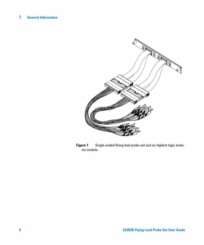
The E5382B is a 17- channel single- ended flying lead probe set, compatible with the Agilent 90- pin logic analyzers such as Agilent 16850- series, U4154A, 16950B, and 16951B logic analysis modules. The E5382B enables you to acquire signals from randomly located points in your target system.
Examples - Four E5382Bs are required to support all 68 channels of one 16950B, 16951B, or 16960A. Two E5382Bs are required to support all 34 channels of one 16851A logic analyzer, four E5382Bs for all 68 channels of a 16852A, six E5382Bs for all 102 channels of a 16853A, and eight E5382Bs for all 136 channels of a 16854A.
A variety of accessories are supplied with the E5382B to allow you to access signals on various types of components on your PC board.
5
1 General Information
Figure 1 Single-ended flying lead probe set and an Agilent logic analy-sis module.
6 E5382B Flying Lead Probe Set User Guide

General Information 1
To inspect the probe
1 Inspect the shipping container for damage.
Keep a damaged shipping container or cushioning material until the contents of the shipment have been checked for completeness and the instrument has been checked mechanically and electrically.
2 Check the accessories.
Accessories supplied with the instrument are listed in "Accessories Supplied" later in this chapter.
• If the contents are incomplete or damaged, notify your Agilent Technologies Sales Office.
3 Inspect the probe.
If there is a mechanical damage or defect, or if the probe does not operate properly or pass performance tests, notify your Agilent Technologies Sales Office.
If the shipping container is damaged, or the cushioning materials show signs of stress, notify the carrier as well as your Agilent Technologies Sales Office. Keep the shipping materials for the carrier’s inspection. The Agilent Technologies Office will arrange for repair or replacement at Agilent Technologies’ option without waiting for claim settlement.
E5382B Flying Lead Probe Set User Guide 7

1 General Information
Figure 2 Probe case contents
8 E5382B Flying Lead Probe Set User Guide

General Information 1
Accessories
The following figure shows the accessories supplied with the E5382B Single- ended Flying Lead Probe Set.
Figure 3 Accessories supplied
The following table lists the part numbers for ordering replacement parts and additional accessories.
Replaceable Parts and Additional Accessories
Description Qty Agilent Part Number
Probe Pin Kit 2 E5382-82103
High Frequency Probing Kit (4 resistive signal pins & 4 solder-down grounds)
8 E5382-82101
Ground Extender Kit 20 16517-82105
Grabber Clip Kit 20 16517-82109
Right-angle Ground Lead Kit 20 16517-82106
Cable - Main 1 E5382-61605
Probe Tip to BNC Adapter 1 E9638A
E5382B Flying Lead Probe Set User Guide 9

1 General Information
Characteristics and Specifications
The following characteristics are typical for the probe set.
Characteristics
(1) refer to specifications on specific modes of operation for details on how inputs can be used(2) if using the clock as single-ended, the unused clock input must be grounded and the minimum voltage swing for single-ended clock operation is 250mV p-p
Input Resistance 20 kΩ
Input Capacitance 1.3 pF (accessory-specific, see accessories)
Maximum Recommended State Data Rate 1.5 Gb/s (accessory-specific, see accessories)
Minimum Data Voltage Swing 250 mV p-p
Minimum Diff. Clock Voltage Swing 100 mV p-p each side
Input Dynamic Range -3 Vdc to +5 Vdc
Threshold Accuracy ±(30 mV +2% of setting)
Threshold Range -3.0 V to +5.0 V
Maximum Nondestructive Input Voltage 40 Vdc
Maximum Input Slew Rate 5 V/ns
Clock Input differential (2)
Number of Inputs (1) 17 (1 clock and 16 data)
10 E5382B Flying Lead Probe Set User Guide

General Information 1
General Characteristics
The following general characteristics apply to the probe set.
Environmental Conditions
Figure 4 E5382B Single-ended Flying Lead Probe Set Dimensions
Operating Non-operating
Temperature 0 °C to +55 °C -40 °C to +70 °C
Humidity up to 95% relative humidity(non-condensing) at +40 °C
up to 90% relative humidity at +65 °C
Weight approximately 0.69 kg
Dimensions Refer to the figure below.
Pollution degree 2 Normally only non-conductive pollution occurs. Occasionally, however, a temporary conductivity caused by condensation must be expected.
Indoor use
E5382B Flying Lead Probe Set User Guide 11

1 General Information
To connect and set up the probe set
1 Connect the single- ended probe to the logic analysis module.
Four E5382Bs are required to support all 68 channels of one 16950B, 16951B, or 16960A. Two E5382Bs are required to support all 34 channels of one 16851A logic analyzer, four E5382Bs for all 68 channels of a 16852A, six E5382Bs for all 102 channels of a 16853A, and eight E5382Bs for all 136 channels of a 16854A.
Figure 5 Probe set connected to an analysis module
12 E5382B Flying Lead Probe Set User Guide

General Information 1
2 Set the clock input.
a If you are using a differential clock, select the Clock Threshold button in the analyzer setup screen of the logic analyzer.
Figure 6 Differential threshold
E5382B Flying Lead Probe Set User Guide 13

1 General Information
b If your clock is not differential, ground the unused clock input and set the threshold to the desired level.
Figure 7 User defined threshold
3 Connect the flying leads to your target system.
14 E5382B Flying Lead Probe Set User Guide

E5382B Single-ended Flying Lead Probe SetUser Guide
2Operating the Probe
Introduction 16
130 ohm Resistive Signal Pin (orange) and Solder-down Ground Lead 19
5 cm Resistive Signal Lead and Solder-down Ground Lead 35
Flying Lead and Ground Extender 52
Grabber Clip and Right-angle Ground Lead 66
Grabber Clip and Right-angle Ground Lead 66
Connecting to Coaxial Connectors 81
Combining Grounds 84
This chapter describes the recommended probe configurations in the order of best performance. Select the configuration that works with your target system.
15
2 Operating the Probe
Introduction
The Agilent E5382B single- ended flying lead probe set comes with accessories that trade off flexibility, ease of use, and performance. Discussion and comparisons between four of the most common intended uses of the accessories are included in this chapter. The table that follows is an overview of the trade- offs between the various accessories. Each of the four configurations have been characterized for probe loading effects, probe step response, and maximum usable state speed. For more detailed information, refer to the pages indicated for each configuration.
When simulating circuits that include a load model for the probe, a simplified model of the probe's input impedance can usually be used. The following table contains information for the simplified model of the probe using suggested accessory configurations. For more accurate load models and detailed discussion of each configuration's performance, refer to the pages indicated.
16 E5382B Flying Lead Probe Set User Guide

Operating the Probe 2
Suggested Configurations and Characteristics
Configuration Description
Total lumped input C
Maximum recommended state speed
Details on page
130 Ω ResistiveSignal Pin (orange) and Solder-down Ground Lead
1.3 pF 1.5 Gb/s page 19
5 cm Resistive Signal Lead and Solder-down Ground Lead
1.6 pF 1.5 Gb/s page 35
Flying Lead and Ground Extender
1.4 pF 1.5 Gb/s page 52
E5382B Flying Lead Probe Set User Guide 17

2 Operating the Probe
Grabber Clip and Right-angle Ground Lead
2.0 pF 600 Mb/s page 66
Configuration Description
Total lumped input C
Maximum recommended state speed
Details on page
18 E5382B Flying Lead Probe Set User Guide

Operating the Probe 2
130 ohm Resistive Signal Pin (orange) and Solder-down Ground Lead
This configuration is recommended for hand- held probing of individual test points. Use the resistive signal pin for the signal. For the ground, the preferred method is to use the solder- down ground lead. Alternatively, for ground you could use the right- angle ground lead and a grabber clip as shown on page 66.
Figure 8 Hand-held probing configuration
The 130 Ω resistive signal pin and solder- down ground leads are identical to the accessories for the Agilent 1156A/57A/58A series oscilloscope probes. They provide similar loading effects and characteristics. The accessories for the 1156A/57A/58A probes are compatible with the E5382B probes allowing you to interchange scope and logic analyzer leads.
Input Impedance
The E5382B probes have an input impedance which varies with frequency, and depends on which accessories are being used. The following schematic shows the circuit model for the input impedance of the probe when using the 130 Ω resistive signal pin (orange) and the solder- down ground
E5382B Flying Lead Probe Set User Guide 19

2 Operating the Probe
wire. This model is a simplified equivalent load of the measured input impedance seen by the target.
Figure 9 Equivalent load model
Figure 10 Measured versus modeled input impedance
20 E5382B Flying Lead Probe Set User Guide

Operating the Probe 2
Time Domain Transmission (TDT)
All probes have a loading effect on the circuit when they come in contact with the circuit. Time domain transmission (TDT) measurements are useful for understanding the probe loading effects as seen at the target receiver. The following TDT measurements were made mid- bus on a 50 Ω transmission line load terminated at the receiver. These measurements show how the 130 Ω resistive signal pin (orange) and solder- down ground lead configuration affect the step seen by the receiver for various rise times.
Figure 11 TDT measurement schematic
As the following graphs demonstrate, the 130 Ω resistive signal pin and solder- down ground lead configuration is the least intrusive of the four recommended configurations. The graphs show that the loading effects are virtually invisible for targets with rise times ≥ 500 ps, negligible for targets with 250 ps rise times, and usable for 100 ps rise times. Ultimately, you must determine what is an acceptable amount of distortion of the target signal.
E5382B Flying Lead Probe Set User Guide 21

2 Operating the Probe
Figure 12 TDT measurement at receiver with and without probe load for 100 ps rise time
Figure 13 TDT measurement at receiver with and without probe load for 250 ps rise time
22 E5382B Flying Lead Probe Set User Guide

Operating the Probe 2
Figure 14 TDT measurement at receiver with and without probe load for 500 ps rise time
E5382B Flying Lead Probe Set User Guide 23

2 Operating the Probe
Figure 15 TDT measurement at receiver with and without probe load for 1 ns rise time
Step Inputs
Maintaining signal fidelity to the logic analyzer is critical if the analyzer is to accurately capture data. One measure of a system's signal fidelity is to compare Vin to Vout for various step inputs. For the following graphs, Vin is the signal at the logic analyzer probe tip measured by double probing with an Agilent 54701A probe into an Agilent 54750A oscilloscope (total 2.5 GHz BW). Eye Scan is used to measure Vout, the signal seen by the logic analyzer. The measurements were made on a mid- bus connection to a 50 Ω transmission line load terminated at the receiver. These measurements show the logic analyzer's response while using the 130 Ω resistive signal pin (orange) and solder- down ground lead configuration.
24 E5382B Flying Lead Probe Set User Guide

Operating the Probe 2
Figure 16 Step input measurement schematic
The following graphs demonstrate the logic analyzer's probe response to different rise times. These graphs are included for you to gain insight into the expected performance of the different recommended configurations.
E5382B Flying Lead Probe Set User Guide 25

2 Operating the Probe
Figure 17 Logic analyzer's response to a 100 ps rise time
26 E5382B Flying Lead Probe Set User Guide

Operating the Probe 2
Figure 18 Logic analyzer's response to a 250 ps rise time
NOTE These measurements are not the true step response of the probes. The true step response of a probe is the output of the probe while the input is a perfect step.
E5382B Flying Lead Probe Set User Guide 27

2 Operating the Probe
Figure 19 Logic analyzer's response to a 500 ps rise time
Figure 20 Logic analyzer's response to a 1 ns rise time
28 E5382B Flying Lead Probe Set User Guide

Operating the Probe 2
Eye Opening
The eye opening at the logic analyzer is the truest measure of an analyzer's ability to accurately capture data. Seeing the eye opening at the logic analyzer is possible with Eye Scan. Eye opening helps you know how much margin the logic analyzer has, where to sample and at what threshold. Any probe response that exhibits overshoot and ringing, probe non- flatness, noise and other issues all deteriorate the eye opening seen by the logic analyzer. The following eye diagrams were measured using Eye Scan probed mid- bus on a 50 Ω transmission line load terminated at the receiver. The data patterns were generated using a 223−1 pseudo random bit sequence (PRBS). These measurements show the remaining eye opening at the logic analyzer while using the 130 Ω resistive signal pin (orange) and solder- down ground lead configuration.
NOTE These measurements are not the true step response of the probes. The true step response of a probe is the output of the probe while the input is a perfect step.
E5382B Flying Lead Probe Set User Guide 29

2 Operating the Probe
Figure 21 Eye opening measurement schematic
The logic analyzer Eye Scan measurement uses the same circuitry as the synchronous state mode analysis. Therefore, the eye openings measured are exact representations of what the logic analyzer sees and operates on in state mode. The following measurements demonstrate how the eye opening starts to collapse as the clock rate is increased. At 1500 Mb/s, the eye opening is noticeably deteriorating as jitter on the transitions increase and voltage margins decrease. As demonstrated by the last eye diagram, the 130 Ω resistive signal pin and solder- down ground lead configuration still has a usable eye opening at 1250 Mb/s and minimum signal swing.
30 E5382B Flying Lead Probe Set User Guide

Operating the Probe 2
Figure 22 Logic analyzer eye opening for a PRBS signal of 1 V p-p, 1000 Mb/s data rate
E5382B Flying Lead Probe Set User Guide 31

2 Operating the Probe
Figure 23 Logic analyzer eye opening for a PRBS signal of 1 V p-p, 1250 Mb/s data rate
32 E5382B Flying Lead Probe Set User Guide

Operating the Probe 2
Figure 24 Logic analyzer eye opening for a PRBS signal of 1 V p-p, 1500 Mb/s data rate
E5382B Flying Lead Probe Set User Guide 33

2 Operating the Probe
Figure 25 Logic analyzer eye opening for a PRBS signal of 250 mV, 1250 Mb/s data rate
34 E5382B Flying Lead Probe Set User Guide

Operating the Probe 2
5 cm Resistive Signal Lead and Solder-down Ground Lead
This configuration is recommended for accessing components such as IC leads or surface- mount component leads for hands- off probing.
Figure 26 Surface-mount probe configuration
The 5cm resistive signal lead and the solder- down ground leads are identical to the accessories for the Agilent 1156A/57A/58A oscilloscope probes. They provide similar loading effects and characteristics. The accessories for the 1156A/57A/58A oscilloscope probes are compatible with the E5382B probes, allowing you to interchange scope and logic analyzer leads.
CAUTION The resistor bends easily. A bent resistor could affect the performance of the 5 cm resistive signal lead.
E5382B Flying Lead Probe Set User Guide 35

2 Operating the Probe
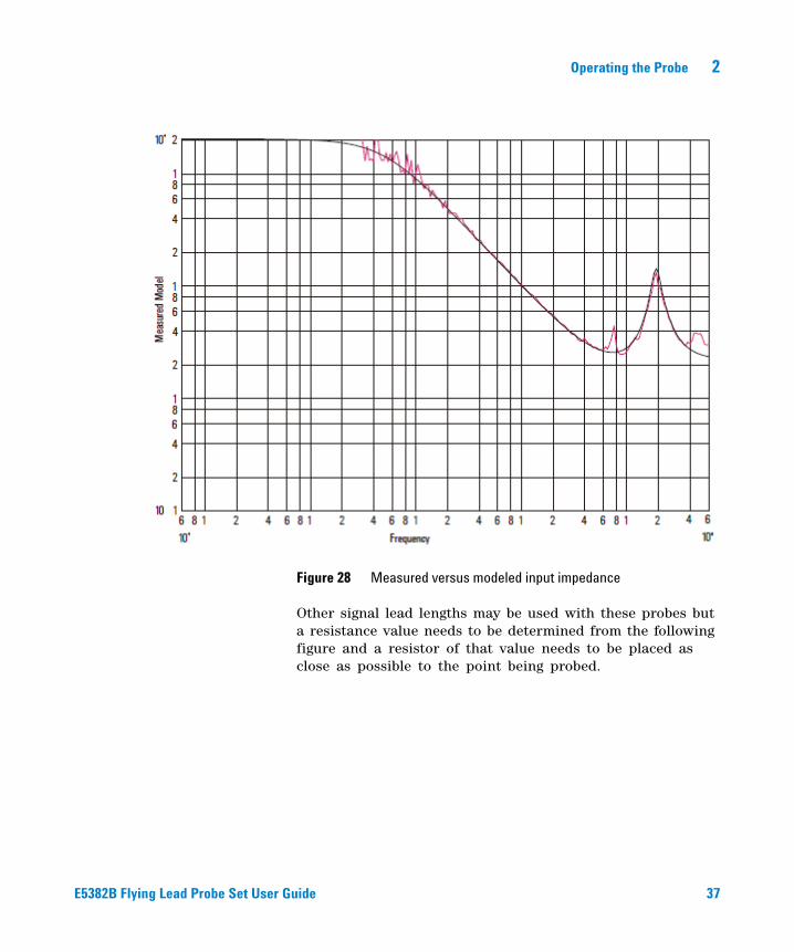
Input Impedance
The E5382B probes have an input impedance which varies with frequency, and depends on which accessories are being used. The following schematic shows the circuit model for the input impedance of the probe when using the SMT solder- down Signal (red) and Ground (black) wires. This model is a simplified equivalent load of the measured input impedance seen by the target.
Figure 27 Equivalent load model
36 E5382B Flying Lead Probe Set User Guide
Operating the Probe 2
Figure 28 Measured versus modeled input impedance
Other signal lead lengths may be used with these probes but a resistance value needs to be determined from the following figure and a resistor of that value needs to be placed as close as possible to the point being probed.
E5382B Flying Lead Probe Set User Guide 37

2 Operating the Probe
Figure 29 Optimum Damping Resistor Value Versus Signal Lead Length
If a resistor is not used, the response of the probe will be very peaked at high frequencies. This will cause overshoot and ringing to be introduced in the step response of waveforms with fast rise times. Use of this probe without a resistor at the point being probed should be limited to measuring only waveforms with slower rise times.
Time Domain Transmission (TDT)
All probes have a loading effect on the circuit when they come in contact with the circuit. Time domain transmission (TDT) measurements are useful for understanding the probe loading effects as seen at the target receiver. The following TDT measurements were made mid- bus on a 50 Ω transmission line load terminated at the receiver. These
38 E5382B Flying Lead Probe Set User Guide

Operating the Probe 2
measurements show how the 5 cm resistive signal lead and solder- down ground lead configuration affect the step seen by the receiver for various rise times.
Figure 30 TDT measurement schematic
The recommended configurations are listed in order of loading on the target. As the following graphs demonstrate, the 5 cm resistive signal lead and solder- down ground lead configuration has the 2nd best loading of the four recommended configurations. The graphs show that the loading effects are virtually invisible for targets with rise times ≥ 500 ps, negligible for targets with 250 ps rise times, and probably still acceptable for 100 ps rise times. Ultimately, you must determine what is an acceptable amount of distortion of the target signal.
E5382B Flying Lead Probe Set User Guide 39

2 Operating the Probe
Figure 31 TDT measurement at receiver with and without probe load for 100 ps rise time
40 E5382B Flying Lead Probe Set User Guide

Operating the Probe 2
Figure 32 TDT measurement at receiver with and without probe load for 250 ps rise time
E5382B Flying Lead Probe Set User Guide 41

2 Operating the Probe
Figure 33 TDT measurement at receiver with and without probe load for 500 ps rise time
42 E5382B Flying Lead Probe Set User Guide

Operating the Probe 2
Figure 34 TDT measurement at receiver with and without probe load for 1 ns rise time
Step Input
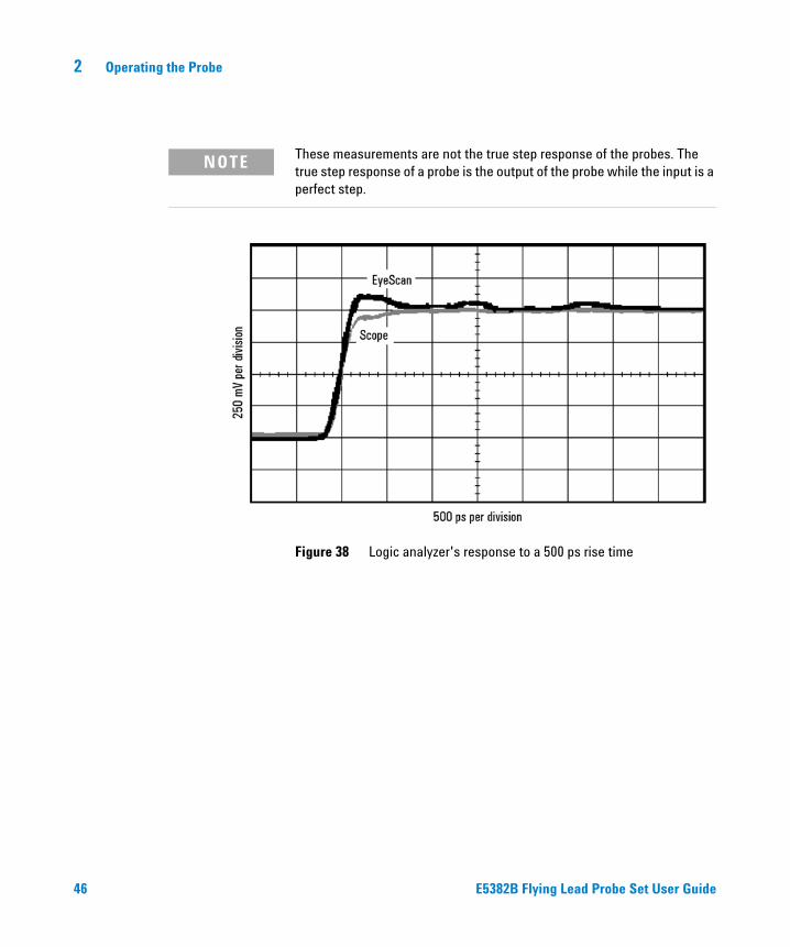
Maintaining signal fidelity to the logic analyzer is critical if the analyzer is to accurately capture data. One measure of a system's signal fidelity is to compare Vin to Vout for various step inputs. For the following graphs, Vin is the signal at the logic analyzer probe tip measured by double probing with an Agilent 54701A probe into an Agilent 54750A oscilloscope (total 2.5 GHz BW). Eye Scan is used to measure Vout, the signal seen by the logic analyzer. The measurements were made on a mid- bus connection to a 50 Ω transmission line load terminated at the receiver. These measurements show the logic analyzer's response while using the 5 cm resistive signal lead and solder- down ground lead configuration.
E5382B Flying Lead Probe Set User Guide 43

2 Operating the Probe
Figure 35 Step input measurement schematic
The following graphs demonstrate the logic analyzer's probe response to different rise times. These graphs are included for you to gain insight into the expected performance of the different recommended configurations.
44 E5382B Flying Lead Probe Set User Guide

Operating the Probe 2
Figure 36 Logic analyzer's response to a 100 ps rise time
Figure 37 Logic analyzer's response to a 250 ps rise time
E5382B Flying Lead Probe Set User Guide 45
2 Operating the Probe
Figure 38 Logic analyzer's response to a 500 ps rise time
NOTE These measurements are not the true step response of the probes. The true step response of a probe is the output of the probe while the input is a perfect step.
46 E5382B Flying Lead Probe Set User Guide

Operating the Probe 2
Figure 39 Logic analyzer's response to a 1 ns rise time
Eye Opening
The eye opening at the logic analyzer is the truest measure of an analyzer's ability to accurately capture data. Seeing the eye opening at the logic analyzer is possible with Eye Scan. Eye opening helps you know how much margin the logic analyzer has, where to sample and at what threshold. Any probe response that exhibits overshoot and ringing, probe non- flatness, noise and other issues all deteriorate the eye opening seen by the logic analyzer. The following eye diagrams were measured using Eye Scan probed mid- bus on a 50 Ω transmission line load terminated at the receiver. The data patterns were generated using a 223−1 pseudo random bit sequence (PRBS). These measurements show the
NOTE These measurements are not the true step response of the probes. The true step response of a probe is the output of the probe while the input is a perfect step.
E5382B Flying Lead Probe Set User Guide 47

2 Operating the Probe
remaining eye opening at the logic analyzer while using the 5cm resistive signal lead and solder- down ground lead configuration.
Figure 40 Eye opening measurement schematic
The logic analyzer Eye Scan measurement uses the same circuitry as the synchronous state mode analysis. Therefore, the eye openings measured are exact representations of what the logic analyzer sees and operates on in state mode. The following measurements demonstrate how the eye opening starts to collapse as the clock rate is increased. At 1500 Mb/s, the eye opening is noticeably deteriorating as jitter on the transitions increase and voltage margins decrease. The bandwidth limiting of the 5 cm resistive signal lead causes more roll- off on the transitions. As demonstrated by the last eye diagram, the 5 cm resistive signal lead and solder- down ground lead configuration still has a usable eye opening at 1250Mb/s and minimum signal swing.
48 E5382B Flying Lead Probe Set User Guide

Operating the Probe 2
Figure 41 Logic analyzer eye opening for a PRBS signal of 1 V p-p, 100 Mb/s data rate
E5382B Flying Lead Probe Set User Guide 49

2 Operating the Probe
Figure 42 Logic analyzer eye opening for a PRBS signal of 1 V p-p, 1250 Mb/s data rate
Figure 43 Logic analyzer eye opening for a PRBS signal of 1 V p-p, 1500 Mb/s data rate
50 E5382B Flying Lead Probe Set User Guide

Operating the Probe 2
Figure 44 Logic analyzer eye opening for a PRBS signal of 250 mV p-p, 1250 Mb/s data rate
E5382B Flying Lead Probe Set User Guide 51

2 Operating the Probe
Flying Lead and Ground Extender
This configuration is recommended when you can provide 0.635 mm (0.025 in.) square or round pins on 2.54 mm (0.1 in.) centers as test points where you wish to connect the probe. Alternately, you may substitute soldered- down wires of similar length (up to 1 cm in length) and expect to achieve similar results.
Figure 45 Pin probing configuration
All of the measurements for the flying lead and ground extender configuration were made with standard surface- mount pins on 0.1- inch centers soldered to the test fixture. The input impedance, TDT response, step response, and eye opening measurements all include the combined load of the probe configuration and the surface- mount pins on the target.
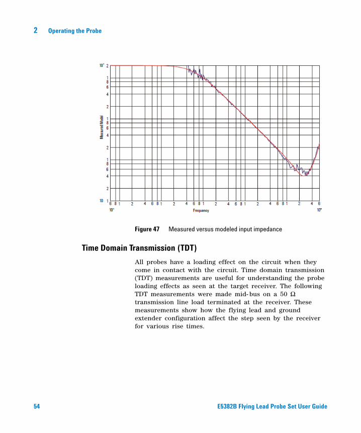
Input Impedance
The E5382B probes have an input impedance which varies with frequency, and depends on which accessories are being used. The following schematic shows the circuit model for the input impedance of the probe when using the ground
52 E5382B Flying Lead Probe Set User Guide

Operating the Probe 2
extender clip. This model is a simplified equivalent load of the measured input impedance seen by the target.
Figure 46 Equivalent load model
E5382B Flying Lead Probe Set User Guide 53
2 Operating the Probe
Figure 47 Measured versus modeled input impedance
Time Domain Transmission (TDT)
All probes have a loading effect on the circuit when they come in contact with the circuit. Time domain transmission (TDT) measurements are useful for understanding the probe loading effects as seen at the target receiver. The following TDT measurements were made mid- bus on a 50 Ω transmission line load terminated at the receiver. These measurements show how the flying lead and ground extender configuration affect the step seen by the receiver for various rise times.
54 E5382B Flying Lead Probe Set User Guide

Operating the Probe 2
Figure 48 TDT measurement schematic
The recommended configurations are listed in order of loading on the target. As the following graphs demonstrate, the flying lead and ground extender configuration has the 3rd best loading of the four recommended configurations. However, because most of the capacitance of this configuration is undamped, the loading is more noticeable than the previous two configurations. The graphs show that the loading effects are negligible for targets with rise times ≥ 500 ps, probably still acceptable for targets with 250 ps rise times, and may be considered significant for 100 ps rise times. Ultimately, you must determine what is an acceptable amount of distortion of the target signal.
E5382B Flying Lead Probe Set User Guide 55

2 Operating the Probe
Figure 49 TDT measurement at receiver with and without probe load for 100 ps rise time
Figure 50 TDT measurement at receiver with and without probe load for 250 ps rise time
50 m
V p
er d
ivis
ion
500 ps per division
without probe
with probe
50 m
V p
er d
ivis
ion
500 ps per division
without probe
with probe
56 E5382B Flying Lead Probe Set User Guide

Operating the Probe 2
Figure 51 TDT measurement at receiver with and without probe load for 500 ps rise time
Figure 52 TDT measurement at receiver with and without probe load for 1 ns rise time
50 m
V p
er d
ivis
ion
500 ps per division
without probe
with probe
50 m
V p
er d
ivis
ion
500 ps per division
without probe
with probe
E5382B Flying Lead Probe Set User Guide 57

2 Operating the Probe
Step Input
Maintaining signal fidelity to the logic analyzer is critical if the analyzer is to accurately capture data. One measure of a system's signal fidelity is to compare Vin to Vout for various step inputs. For the following graphs, Vin is the signal at the logic analyzer probe tip measured by double probing with an Agilent 54701A probe into an Agilent 54750A oscilloscope (total 2.5 GHz BW). Eye Scan is used to measure Vout, the signal seen by the logic analyzer. The measurements were made on a mid- bus connection to a 50 Ω transmission line load terminated at the receiver. These measurements show the logic analyzer's response while using the flying lead and ground extender configuration.
Figure 53 Step measurement schematic
The following graphs demonstrate the logic analyzer's probe response to different rise times. These graphs are included for you to gain insight into the expected performance of the different recommended accessory configurations.
58 E5382B Flying Lead Probe Set User Guide

Operating the Probe 2
Figure 54 Logic analyzer's response to a 100 ps rise time
Figure 55 Logic analyzer's response to a 250 ps rise time
E5382B Flying Lead Probe Set User Guide 59

2 Operating the Probe
Figure 56 Logic analyzer's response to a 500 ps rise time
NOTE These measurements are not the true step response of the probes. The true step response of a probe is the output of the probe while the input is a perfect step.
60 E5382B Flying Lead Probe Set User Guide

Operating the Probe 2
Figure 57 Logic analyzer's response to a 1 ns rise time
Eye Opening
The eye opening at the logic analyzer is the truest measure of an analyzer's ability to accurately capture data. Seeing the eye opening at the logic analyzer is possible with Eye Scan. Eye opening helps you know how much margin the logic analyzer has, where to sample and at what threshold. Any probe response that exhibits overshoot and ringing, probe non- flatness, noise and other issues all deteriorate the eye opening seen by the logic analyzer. The following eye diagrams were measured using Eye Scan probed mid- bus on a 50 Ω transmission line load terminated at the receiver. The data patterns were generated using a 223−1 pseudo random bit sequence (PRBS). These measurements show the remaining eye opening at the logic analyzer while using the flying lead and ground extender configuration.
NOTE These measurements are not the true step response of the probes. The true step response of a probe is the output of the probe while the input is a perfect step.
E5382B Flying Lead Probe Set User Guide 61

2 Operating the Probe
Figure 58 Eye opening measurement schematic
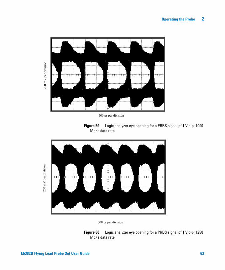
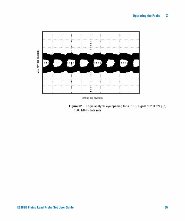
The logic analyzer Eye Scan measurement uses the same circuitry as the synchronous state mode analysis. Therefore, the eye openings measured are exact representations of what the logic analyzer sees and operates on in state mode. The following measurements demonstrate how the eye opening starts to collapse as the clock rate is increased. The peaking observed with this configuration on the preceding step- response graphs helps to preserve the eye opening out to 1.5 Gb/s. At 1500 Mb/s the eye opening is still as large as could be hoped for. As demonstrated by the last eye diagram, the flying lead and ground extender configuration still has no noticeable deterioration at 1500 Mb/s and minimum signal swing.
62 E5382B Flying Lead Probe Set User Guide
Operating the Probe 2
Figure 59 Logic analyzer eye opening for a PRBS signal of 1 V p-p, 1000 Mb/s data rate
Figure 60 Logic analyzer eye opening for a PRBS signal of 1 V p-p, 1250 Mb/s data rate
250
mV
per
div
isio
n
500 ps per division
250
mV
per
div
isio
n
500 ps per division
E5382B Flying Lead Probe Set User Guide 63

2 Operating the Probe
Figure 61 Logic analyzer eye opening for a PRBS signal of 1 V p-p, 1500 Mb/s data rate
250
mV
per
div
isio
n
500 ps per division
64 E5382B Flying Lead Probe Set User Guide
Operating the Probe 2
Figure 62 Logic analyzer eye opening for a PRBS signal of 250 mV p-p, 1500 Mb/s data rate
250
mV
per
div
isio
n
500 ps per division
E5382B Flying Lead Probe Set User Guide 65

2 Operating the Probe
Grabber Clip and Right-angle Ground Lead
Using the grabber clip for the signal and the right- angle for the ground gives you the greatest flexibility for attaching the probe to component leads, however as you can see from the following information, the signal quality is compromised the most severely by this configuration.
Figure 63 Grabber configuration
This configuration is provided as a convenient method of attaching to systems with slower rise times. The response of the probe is severely over- peaked. The load on the target is also the most severe of the 4 recommended configurations. As will be demonstrated in the following sets of measurements, the grabber clip and right angle ground lead configuration is only for systems with rise times slower than 1ns or effective clock rates less than 600Mb/s.
NOTE It is critical to maintain good probing techniques on the clock signal. If the clock being probed has <1 ns rise times, use an alternative configuration for probing.
66 E5382B Flying Lead Probe Set User Guide

Operating the Probe 2
Input Impedance
The E5382B probes have an input impedance which varies with frequency, and depends on which accessories are being used. The following schematic shows the circuit model for the input impedance of the probe when using the SMD IC grabber and the right- angle ground lead. This model is a simplified equivalent load of the measured input impedance seen by the target.
Figure 64 Equivalent load model
E5382B Flying Lead Probe Set User Guide 67

2 Operating the Probe
Figure 65 Measured versus modeled input impedance
Time Domain Transmission (TDT)
All probes have a loading effect on the circuit when they come in contact with the circuit. Time domain transmission (TDT) measurements are useful for understanding the probe loading effects as seen at the target receiver. The following TDT measurements were made mid- bus on a 50 Ω transmission line load terminated at the receiver. These measurements show how the grabber clip and right- angle ground lead configuration affect the step seen by the receiver for various rise times.
2
186
10 4
4
2
186
4
2
1864
2
10 1
Mea
sured
Mod
el
10 4
6 8 1 2 4 6 8 1 2 4 6 8 1Frequency
2 4 6 8 1 2 4 6 8 1 2 4 610 9
68 E5382B Flying Lead Probe Set User Guide

Operating the Probe 2
Figure 66 TDT measurement schematic
The recommended configurations are listed in order of loading on the target. As the following graphs demonstrate, the grabber clip and right angle ground lead configuration has the worst loading of the four recommended configurations. The grabber clip is a fairly long length of undamped wire, which presents a much more significant load on the target than the previous three configurations. The graphs show that the loading effects are noticeable even for targets with 1ns rise times. Ultimately, you must determine what is an acceptable amount of distortion of the target signal.
E5382B Flying Lead Probe Set User Guide 69

2 Operating the Probe
Figure 67 TDT measurement at receiver with and without probe load for 100 ps rise time
Figure 68 TDT measurement at receiver with and without probe load for 250 ps rise time
50 m
V p
er d
ivis
ion
500 ps per division
without probe
with probe
50 m
V p
er d
ivis
ion
500 ps per division
without probe
with probe
70 E5382B Flying Lead Probe Set User Guide

Operating the Probe 2
Figure 69 TDT measurement at receiver with and without probe load for 500 ps rise time
Figure 70 TDT measurement at receiver with and without probe load for 1 ns rise time
50 m
V p
er d
ivis
ion
500 ps per division
without probe
with probe
50 m
V p
er d
ivis
ion
500 ps per division
without probe
with probe
E5382B Flying Lead Probe Set User Guide 71

2 Operating the Probe
Step Input
Maintaining signal fidelity to the logic analyzer is critical if the analyzer is to accurately capture data. One measure of a system's signal fidelity is to compare Vin to Vout for various step inputs. For the following graphs, Vin is the signal at the logic analyzer probe tip measured by double probing with an Agilent 54701A probe into an Agilent 54750A oscilloscope (total 2.5 GHz BW). Eye Scan is used to measure Vout, the signal seen by the logic analyzer. The measurements were made on a mid- bus connection to a 50 Ω transmission line load terminated at the receiver. These measurements show the logic analyzer's response while using the grabber clip and right- angle ground lead configuration.
Figure 71 Step measurement schematic
The following graphs demonstrate the logic analyzer's probe response to different rise times. These graphs are included for you to gain insight into the expected performance of the different recommended accessory configurations, particularly for the grabber clip and right- angle ground lead configuration. As the following graphs will demonstrate, the use of the undamped grabber clip results in excessive overshoot and ringing at the logic analyzer for targets with < 1 ns rise times.
72 E5382B Flying Lead Probe Set User Guide

Operating the Probe 2
Figure 72 Logic analyzer's response to a 100 ps rise time
Figure 73 Logic analyzer's response to a 250 ps rise time
E5382B Flying Lead Probe Set User Guide 73

2 Operating the Probe
Figure 74 Logic analyzer's response to a 500 ps rise time
NOTE These measurements are not the true step response of the probes. The true step response of a probe is the output of the probe while the input is a perfect step.
74 E5382B Flying Lead Probe Set User Guide

Operating the Probe 2
Figure 75 Logic analyzer's response to a 1 ns rise time
Eye Opening
The eye opening at the logic analyzer is the truest measure of an analyzer's ability to accurately capture data. Seeing the eye opening at the logic analyzer is possible with Eye Scan. Eye opening helps you know how much margin the logic analyzer has, where to sample and at what threshold. Any probe response that exhibits overshoot and ringing, probe non- flatness, noise and other issues all deteriorate the eye opening seen by the logic analyzer. The following eye diagrams were measured using Eye Scan probed mid- bus on a 50 Ω transmission line load terminated at the receiver. The data patterns were generated using a 223−1 pseudo random
NOTE These measurements are not the true step response of the probes. The true step response of a probe is the output of the probe while the input is a perfect step.
E5382B Flying Lead Probe Set User Guide 75

2 Operating the Probe
bit sequence (PRBS). These measurements show the remaining eye opening at the logic analyzer while using the grabber clip and right- angle ground lead configuration.
Figure 76 Eye opening measurement schematic
The logic analyzer Eye Scan measurement uses the same circuitry as the synchronous state mode analysis. Therefore, the eye openings measured are exact representations of what the logic analyzer sees and operates on in state mode. The following measurements demonstrate how the eye opening starts to collapse as the clock rate is increased. The severe overshoot and ringing observed with this configuration on the preceding step- response graphs deteriorates the eye opening for faster rise times. At 500 ps rise times the eye opening shows excessive ring- back and collapsing of the eye. Therefore, it is recommended that this configuration not be used for rise times faster than 1ns or clock rates in excess of 600 Mb/s. The analyzer may still function at faster speeds, but will not meet state speed and setup/hold specifications.
76 E5382B Flying Lead Probe Set User Guide

Operating the Probe 2
NOTE it is critical to maintain good probing techniques on the clock signal. if the clock being probed has < 1 ns rise times, use an alternative configuration for probing.
E5382B Flying Lead Probe Set User Guide 77

2 Operating the Probe
Figure 77 Logic analyzer eye opening for a PRBS signal of 1 V p-p, 500 Mb/s data rate, 1 ns rise time
250
mV
per
div
isio
n
500 ps per division
78 E5382B Flying Lead Probe Set User Guide

Operating the Probe 2
Figure 78 Logic analyzer eye opening for a PRBS signal of 1 V p-p, 500 Mb/s data rate, 500 ps rise time
250
mV
per
div
isio
n
500 ps per division
E5382B Flying Lead Probe Set User Guide 79

2 Operating the Probe
Figure 79 Logic analyzer eye opening for a PRBS signal of 1 V p-p, 600 Mb/s data rate, 1 ns rise time
Figure 80 Logic analyzer eye opening for a PRBS signal of 250 mV, 600 Mb/s data rate, 1 ns rise time
250
mV
per
div
isio
n
500 ps per division
250
mV
per
div
isio
n
500 ps per division
80 E5382B Flying Lead Probe Set User Guide

Operating the Probe 2
Connecting to Coaxial Connectors
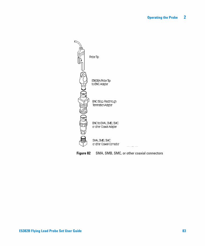
You can use the Agilent E9638A to adapt the probe tip to a BNC connector. The adapter and the BNC connector itself will add significant capacitance to the probe load. You can generally assume (though not always) that a BNC connector is intended to form a part of a transmission line terminated in 50 Ω (the characteristic impedance of BNC connectors is 50 Ω). So, the best solution for maintaining signal integrity is to terminate the line in 50 Ω after the BNC connector and a close as possible to the probe tip. That technique minimizes the length of the unterminated stub past the termination. The following picture shows the recommended configuration to achieve this.
NOTE This configuration has not been characterized for target loading or logic analyzer performance. Therefore no recommendations are being made or implied as to the expected performance of this configuration.
E5382B Flying Lead Probe Set User Guide 81

2 Operating the Probe
Figure 81 BNC connector
82 E5382B Flying Lead Probe Set User Guide
Operating the Probe 2
Figure 82 SMA, SMB, SMC, or other coaxial connectors
E5382B Flying Lead Probe Set User Guide 83

2 Operating the Probe
Combining Grounds
It is essential to ground every tip that is in use. For best performance at high speeds, every tip should be grounded individually to ground in the system under test. For convenience in connecting grounds, you can use the ground connector, Agilent part number 16515- 27601, to combine four probe tip grounds to connect to one ground point in the system under test.
Using the 16515- 27601 to combine grounds will have some negative impact on performance due to coupling caused by common ground return currents. The exact impact depends on the signals being tested and the configuration of the test, so it is impossible to predict accurately. In general, the faster the rise time of the signals under test, the greater the risk of coupling.
In no case should more than four tip grounds be combined through one 16515- 27601 to connect to ground in the system under test.
84 E5382B Flying Lead Probe Set User Guide

Operating the Probe 2
E5382B Flying Lead Probe Set User Guide 85

2 Operating the Probe
86 E5382B Flying Lead Probe Set User Guide
Safety Information
Safety Information
The following general safety precautions must be observed during all phases of operation of this instrument. Failure to comply with these precautions or with specific warnings or operating instructions in the product manuals violates safety standards of design, manufacture, and intended use of the instrument. Agilent Technologies assumes no liability for the customer's failure to comply with these requirements. Product manuals are provided with your instrument on CD- ROM and/or in printed form. Printed manuals are an option for many products. Manuals may also be available on the Web. Go to www.agilent.com and type in your product number in the Search field at the top of the page.
General Do not use this product in any manner not specified by the manufacturer. The protective features of this product may be impaired if it is used in a manner not specified in the operation instructions.
Before Applying Power Verify that all safety precautions are taken. Make all connections to the unit before applying power. Note the instrument's external markings described in “Safety Symbols”.
Ground the Instrument If your product is provided with a grounding type power plug, the instrument chassis and cover must be connected to an electrical ground to minimize shock hazard. The ground pin must be firmly connected to an electrical ground (safety ground) terminal at the power outlet. Any interruption of the protective (grounding) conductor or disconnection of the protective earth terminal will cause a potential shock hazard that could result in personal injury.
E5382B Flying Lead Probe Set User Guide 87
Safety Information
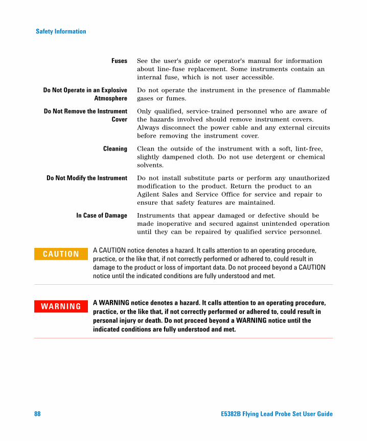
Fuses See the user's guide or operator's manual for information about line- fuse replacement. Some instruments contain an internal fuse, which is not user accessible.
Do Not Operate in an ExplosiveAtmosphere
Do not operate the instrument in the presence of flammable gases or fumes.
Do Not Remove the InstrumentCover
Only qualified, service- trained personnel who are aware of the hazards involved should remove instrument covers. Always disconnect the power cable and any external circuits before removing the instrument cover.
Cleaning Clean the outside of the instrument with a soft, lint- free, slightly dampened cloth. Do not use detergent or chemical solvents.
Do Not Modify the Instrument Do not install substitute parts or perform any unauthorized modification to the product. Return the product to an Agilent Sales and Service Office for service and repair to ensure that safety features are maintained.
In Case of Damage Instruments that appear damaged or defective should be made inoperative and secured against unintended operation until they can be repaired by qualified service personnel.
CAUTION A CAUTION notice denotes a hazard. It calls attention to an operating procedure, practice, or the like that, if not correctly performed or adhered to, could result in damage to the product or loss of important data. Do not proceed beyond a CAUTION notice until the indicated conditions are fully understood and met.
WARNING A WARNING notice denotes a hazard. It calls attention to an operating procedure, practice, or the like that, if not correctly performed or adhered to, could result in personal injury or death. Do not proceed beyond a WARNING notice until the indicated conditions are fully understood and met.
88 E5382B Flying Lead Probe Set User Guide

Safety Information
Safety Symbols
Table 1Description of Safety related symbols that may appear on a product (Sheet 1 of 3)
Symbol Description
Direct current
Alternating current
Both direct and alternating current
Three phase alternating current
Earth ground terminal
Protective earth ground terminal
Frame or chassis ground terminal
Terminal is at earth potential
Equipotentiality
N Neutral conductor on permanently installed equipment
L Line conductor on permanently installed equipment
On (mains supply)
E5382B Flying Lead Probe Set User Guide 89
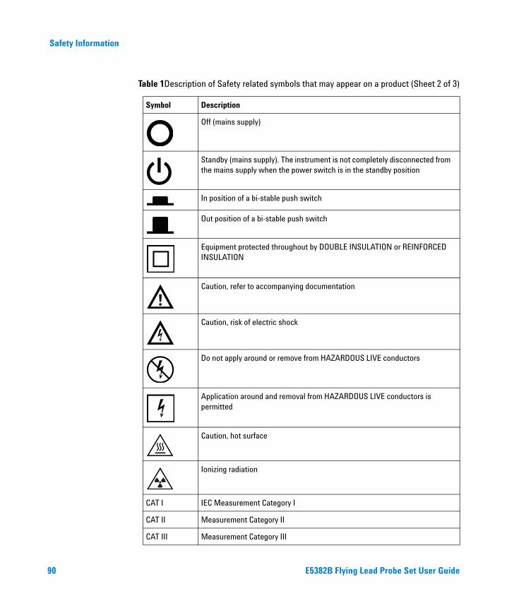
Safety Information
Off (mains supply)
Standby (mains supply). The instrument is not completely disconnected from the mains supply when the power switch is in the standby position
In position of a bi-stable push switch
Out position of a bi-stable push switch
Equipment protected throughout by DOUBLE INSULATION or REINFORCED INSULATION
Caution, refer to accompanying documentation
Caution, risk of electric shock
Do not apply around or remove from HAZARDOUS LIVE conductors
Application around and removal from HAZARDOUS LIVE conductors is permitted
Caution, hot surface
Ionizing radiation
CAT I IEC Measurement Category I
CAT II Measurement Category II
CAT III Measurement Category III
Table 1Description of Safety related symbols that may appear on a product (Sheet 2 of 3)
Symbol Description
90 E5382B Flying Lead Probe Set User Guide

Safety Information
CAT IV Measurement Category IV
Table 1Description of Safety related symbols that may appear on a product (Sheet 3 of 3)
Symbol Description
E5382B Flying Lead Probe Set User Guide 91

Safety Information
Informations relatives à la sécurité
Les consignes de sécurité générales présentées dans cette section doivent être appliquées au cours des différentes phases d'utilisation de cet appareil. Le non- respect de ces précautions ou des avertissements et consignes d'utilisation spécifiques mentionnés dans les manuels des produits constitue une violation des normes de sécurité relatives à la conception, à la fabrication et à l'usage normal de l'instrument. Agilent Technologies ne saurait être tenu responsable du non- respect de ces consignes. Les manuels des produits sont fournis avec votre instrument sur CD- ROM et/ou en version papier. Les versions papier des manuels sont en option pour de nombreux produits. Certains manuels sont également disponibles en ligne. Pour y accéder, allez sur le site www.agilent.com et saisissez la référence de votre produit dans le champ Rechercher qui se trouve en haut de la page.
Généralités Utilisez ce produit uniquement dans le cadre prévu par le fabricant. Si vous ne respectez pas les instructions d'utilisation, les fonctions de sécurité du produit risquent d'être inhibées.
Avant la mise sous tension Vérifiez que vous avez bien respecté toutes les consignes de sécurité. Faites tous les branchements au niveau de l'appareil avant de mettre ce dernier sous tension. Tenez compte des marquages externes à l'instrument décrits à la section «Symboles de sécurité».
Mise à la terre de l'instrument Si une prise de mise à la terre est fournie avec le produit, le châssis et le capot de l'instrument doivent être reliés à la terre afin de limiter les risques d'électrocution. Le contact à la terre doit être solidement connecté à une borne de terre (de sécurité) au niveau de la prise de courant . Toute interruption du conducteur de protection (mise à la terre) ou tout débranchement de la borne de terre de protection donne lieu à un risque d'électrocution pouvant entraîner des blessures graves.
92 E5382B Flying Lead Probe Set User Guide

Safety Information
Fusibles Pour obtenir des instructions sur le changement des fusibles de ligne, consultez le guide de l'utilisateur ou le manuel d'instructions. Certains instruments comportent un fusible interne inaccessible à l'utilisateur.
Ne pas utiliser en atmosphèreexplosive
N'utilisez pas l'instrument en présence de gaz ou de vapeurs inflammables.
Ne pas démonter le capot del'instrument
Seules des personnes qualifiées, formées à la maintenance et conscientes des risques d'électrocution encourus sont autorisées à démonter les capots de l'instrument. Débranchez toujours le cordon d'alimentation secteur et tous les circuits externes avant de démonter le capot de l'instrument.
Nettoyage Nettoyez la partie externe de l'instrument à l'aide d'un chiffon doux et non pelucheux, légèrement humidifié. N'utilisez pas de détergents ou de solvants chimiques.
Ne pas modifier l'instrument N'installez pas de composants de remplacement et n'apportez aucune modification non autorisée à l'appareil. Pour toute opération de maintenance ou de réparation, renvoyez l'appareil à un bureau de vente et de service après- vente Agilent, afin d'être certain que les fonctions de sécurité seront maintenues.
En cas de dommages Les instruments endommagés ou défectueux doivent être désactivés et protégés contre toute utilisation involontaire jusqu'à ce qu'ils aient été réparés par une personne qualifiée.
La mention ATTENTION indique un risque. Si la manoeuvre ou le procédé correspondant n'est pas exécuté correctement, il peut y avoir un risque de dommages à l'appareil ou de perte de données importantes. En présence de la mention ATTENTION, il convient de s'interrompre tant que les conditions indiquées n'ont pas été parfaitement comprises et respectées.
La mention AVERTISSEMENT signale un danger pour la sécurité de l'opérateur. Si la manœuvre ou le procédé correspondant n'est pas exécuté correctement, il peut y avoir un risque pour la santé des personnes. En présence d'une mention AVERTISSEMENT, il convient de s'interrompre tant que les conditions indiquées n'ont pas été parfaitement comprises et respectées.
E5382B Flying Lead Probe Set User Guide 93

Safety Information
Symboles de sécurité:
Table 2Description des Symboles de Sécurité qui pourraient apparaître sur le produit. (Sheet 1 of 3)
Symboles Description
Courant continu.
Courant alternatif.
Courant continu et alternatif.
Courant alternative triphasé.
Borne de terre (masse).
Borne de terre de protection.
Borne de terre reliée au cadre ou au châssis.
Borne au potentiel de la terre.
Equipotentialité
N Conducteur neutre sur un équipement installé à demeure
L Conducteur de phase sur un équipement installé à demeure.
Alimentation en marche.
94 E5382B Flying Lead Probe Set User Guide

Safety Information
Alimentation à l'arrêt.
Alimentation en mode veille. Lorsque l'interrupteur est en mode veille, l'unité n'est pas complètement déconnectée de l'alimentation secteur.
Position Marche d'un interrupteur par bouton poussoir bi-stable.
Position Arrêt d'un interrupteur par bouton poussoir bi-stable.
Appareil entièrement protégé par DOUBLE ISOLATION ou ISOLATION RENFORCÉE
Attention. Consultez la documentation fournie.
Attention, danger d'électrocution.
Ne pas appliquer ou enlever sur des conducteurs SOUS TENSION DANGEREUSE
Application ou retrait autorisés sur les conducteurs SOUS TENSION DANGEREUSE
Attention, surface chaude
Rayonnement ionisant
CAT I Appareil de mesure de catégorie I selon la norme CEI applicable
CAT II Appareil de mesure de catégorie II selon la norme CEI applicable
CAT III Appareil de mesure de catégorie III selon la norme CEI applicable
Table 2Description des Symboles de Sécurité qui pourraient apparaître sur le produit. (Sheet 2 of 3)
Symboles Description
E5382B Flying Lead Probe Set User Guide 95

Safety Information
CAT IV Appareil de mesure de catégorie IV selon la norme CEI applicable
Table 2Description des Symboles de Sécurité qui pourraient apparaître sur le produit. (Sheet 3 of 3)
Symboles Description
96 E5382B Flying Lead Probe Set User Guide

Index
Aaccessories
additional, 9supplied, 9
BBerg strip, 52, 66BNC adapter, 9
Ccharacteristics
of probe, 10, 11of suggested configurations, 17
clock, 10clock input, 12configuration
130 ohm resistive signal pin & solder-down ground lead, 19
5 cm resistive signal pin & solder-down ground lead, 35
flying lead and ground extender, 52grabber clip and right-angle ground
lead, 66hand-held probing, 19pin probing, 52surface-mount probing, 35
configurations, suggested, 17connecting to logic analyzer, 12
Ddamage
to the probe, 7to the resistor, 35
differential threshold, 12dimensions, 11
Eenvironmental characteristics, 11eye opening, 29, 47, 61, 75
Fflying lead, 17, 52flying lead and grabber clip, 66flying lead and signal pin, 19
Ggeneral characteristics, 11grabber clip, 17, 66ground
extender, 17, 52lead, 19right angle, 17, 66solder down, 17, 19, 35
Hhand-held probing, 19
IIC probing, 35input impedance, 19, 36, 52, 67inspecting probe, 7
Ooperating environment, 11ordering accessories, 9
Ppart numbers for accessories, 9pin probing, 52
probecase contents, 7characteristics, 10, 11inspection, 7setup, 12
probingBerg strip, 52Berg strip and IC, 66coaxial connectors, 83grabber clip, 66IC and pins, 66IC and surface mount, 66IC and test point, 35pins, 52SMA, SMB,SMC connectors, 83surface-mount components, 35test points, 19
Rrepair or replacement, 7replaceable parts, 9resistive signal
lead, 5 cm, 17, 35pin, 130 ohm, 17, 19
Ssetting up the probe & logic analyzer, 12SMA,SMB,SMC connectors, 83solder-down ground, 19, 35specifications, 10state data rate, 10step input, 24, 43, 58, 72suggested configurations, 17surface-mount probing, 35
TTDT, 21, 38, 54, 68test point, 19, 35
E5382B Flying Lead Probe Set User Guide 97

Index
thresholdaccuracy, 10differential, 12range, 10user defined, 14
Uuser defined threshold, 14
Wweight, 11
98 E5382B Flying Lead Probe Set User Guide