Embed Size (px)
DESCRIPTION
communication lab
Citation preview

MOOKAMBIGAI COLLEGE OF ENGINEERING
DEPARTMENT OF ECE
EC2307 COMMUNICATION SYSTEMS LAB MANUAL
FIFTH SEMESTER
1

Block diagram of AM modulator/demodulator:
2

AMPLITUDE MODULATION AND DEMODULATION
Ex No :
Date :
Aim :
To generate amplitude modulated signal and demodulate it to get the original signal.
Apparatus Required :
Modules ACL-01 & ACL-02
Power supply
20 MHz Oscilloscope
Connecting links
Theory :
The modulation is simply a method of combining two different signals and is used in the transmitter section of a communication system. The two signals that are used are the information signal and the carrier signal.
Amplitude Modulation is the simplest form of signal processing in which the carrier amplitude is simply changed according to the amplitude of the information signal hence the name Amplitude modulation. When the information signals amplitude is increased the carrier signals amplitude is increased and when the information signals amplitude is decreased the carrier signals amplitude is decreased.
The purpose of any detector or demodulator is to recover the original modulating signal with the minimum of distortion and interference. The simplest way of dealing with an AM signal is to use a simple half- wave rectifier circuit. If the signal were simply passed through a diode to a resistive load, the output would be a series of half-cycle pulses at carrier frequency. So the diode is followed by a filter, typically a capacitor and resistor in parallel. The capacitor is charged by the diode almost to the peak value of the carrier cycles and the output therefore follows the envelope of the amplitude modulation.
3

Model Graph:
Observation:
Amplitude (v) Time period (ms) Frequency
Message signal
Carrier signal
AM signal
Demodulated signal
4

Modulation index = (H-h/H+h)x100
Procedure :
1. Connections are given as per the block diagram.
2. Keep the switch faults of ACL-01 and ACL-02 in OFF position.
3. Switch on the power supply and carry out the following presetting:
a. Function generator : Sine LEVEL about 0.5 Vpp; FREQ about 1 KHz
b. VCO : LEVEL about 2 Vpp; FREQ about 850 KHZ, switch on 1500 KHz
c. Balanced Modulator 1 : CARRIER NULL completely rotates clockwise or counter clockwise, so that the modulator is unbalanced and the AM signal with not suppressed carrier is obtained across the output. Adjust the OUTLEVEL to obtain an AM signal across the output whose amplitude is 100m Vpp.
d. Local oscillator (ACL-02) : 1300 KHz, 2 V
4. Observe the modulated signal using CRO at the OUT post of balanced modulator 1 and demodulated signal at the envelope detector.
5. Vary the frequency and amplitude of modulating signal and check the corresponding variations of modulated and demodulated signal. Calculate the modulation index.
Result:
Thus the amplitude modulated signal was generated and demodulated to get the original signal.
5

Block diagram of FM Modulation/Demodulation :
6

FREQUENCY MODULATION AND DEMODULATION
Ex No :
Date :
Aim :
To generate frequency modulated signal and demodulate it to get the original signal.
Apparatus Required :
Modules ACL-03 & ACL-04
Power supply
20 MHz Oscilloscope
Connecting links
Theory :
Frequency modulation is also called as angle modulation. Frequency modulation is defined as changing the frequency of the carrier with
respect to the message signal amplitude. Here the amplitude of the carrier remains fixed & timing parameter frequency is
varied. When the modulating signal has zero amplitude, then the carrier has frequency of Fc as amplitude of the modulating signal increases. The frequency of the carrier increases, similarly, as the amplitude of the modulating signal decreases, the frequency of the carrier decreases.
The modulation index is defined as the ratio of the maximum frequency deviation to the modulating frequency. The maximum frequency deviation is the shift from center frequency Fc when the amplitude of the modulating signal is maximum.
7

Model graph:
Observation:
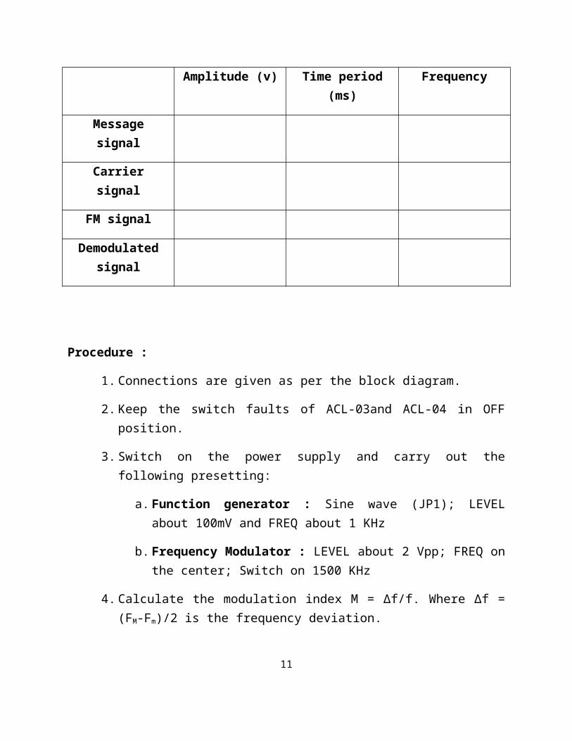
Amplitude (v) Time period (ms) Frequency
Message signal
Carrier signal
FM signal
Demodulated signal
8

Procedure :
1. Connections are given as per the block diagram.
2. Keep the switch faults of ACL-03and ACL-04 in OFF position.
3. Switch on the power supply and carry out the following presetting:
a. Function generator : Sine wave (JP1); LEVEL about 100mV and FREQ about 1 KHz
b. Frequency Modulator : LEVEL about 2 Vpp; FREQ on the center; Switch on 1500 KHz
4. Calculate the modulation index M = ∆f/f. Where ∆f = (FM-Fm)/2 is the frequency deviation.
5. Vary the frequency of modulating signal and check the corresponding variations of modulated and demodulated signal. Calculate the modulation index.
6. Connect the output of frequency modulator FM/RF OUT post to the input of RF IN of mixer in ACL-04
7. Carry out the following presetting:
a. Frequency modulator : Switch on 500 KHz; LEVEL about 1 Vpp; FREQ about 450 KHz
b. Frequency demodulator in Foster-Seeley mode (Jumpers in FS position).
c. Function generator : Sine wave (JP1); LEVEL about 100m Vpp; FREQ about 500 Hz
d. Local Oscillator : LEVEL about 1Vpp; FREQ about 1000 KHz on center
8. Observe demodulated signal at the output of filter.
Result:Thus the frequency modulated signal was generated and demodulated to get the original signal.
9

Circuit diagram:
Modulator
Demodulator
Observation
Signal Amplitude (v) Time period (ms) Frequency (KHz)Message signal
Carrier signal Ton=Toff=
PAM signal Vmax=Vmin=
Demodulated signal
10
PULSE AMPLITUDE MODULATION
Ex No :
Date :
Aim :
To generate pulse amplitude modulated signal and demodulate it to get the original signal.
Apparatus Required :
Apparatus Range Quantity
Transistor BC107 1
Resistor 47KΩ, 22kΩ, 3.3kΩ Each 1
Capacitor 0.1μF 1
DRB - 1
Power supply - 1
Connecting wires - As required
Bread board - 1
CRO 20 MHz 1
AFO - 1
Theory:
In pulse amplitude modulation, the amplitudes of regularly spaced rectangular pulses vary with the instantaneous sample values of a continuous message signal in a oneto one fashion. The pulse in PAM can be of rectangular or the type that we have arrival in natural sampling. The carrier under goes amplitude modulation in PAM. The width of the pulse remains fixed. Natural sample method is used here to generate the PAM signal. The diodes are used as a switching element. If the closing time t of the diode approaches zero, the output gives only the instantaneous value.
11
Model Graph:
Design:
12

Since the width of the pulse approaches zero. The instantaneous sampling gives train of impulses. The area of each sampled section is equal to the instantaneous value of the signal input. This signal is modulatedwith the message signal. Thus we get the PAM output.
Procedure:1. Set the supply voltage as 12v and make the connections as per the circuit
diagram2. Give a low frequency sinusoidal signal as modulating signal and high
frequency square wave as a carrier signal.3. Obtain the output PAM waveform on the CRO.4. Measure the amplitude and time period of the modulating signal and carrier
signal.5. Measure the max and min amplitude of the PAM signal.6. Connect the demodulation circuit as shown in figure.7. Connect the output of the modulator circuit to the input of the demodulator
circuit and obtain the demodulation output.8. Plot the waveform in graph.
Result:
Thus the pulse amplitude modulated signal was generated and demodulated to get the original signal.
13

Pin Diagram:
Circuit Diagram:
PWM Modulator
PWM Demodulator
14

PULSE WIDTH MODULATION
Ex No :
Date :
Aim :
To generate pulse width modulated signal and demodulate it to get the original signal.
Apparatus Required :
Apparatus Range Quantity
Timer IC555 1
Resistor 1KΩ, 10KΩ Each 1
Capacitor 0.01μF, 10 μF Each 1
DRB - 1
Power supply - 1
Connecting wires - As required
Bread board - 1
CRO 20 MHz 1
AFO - 1
Theory:
The PWM is also known as pulse duration modulation. It modulates the time parameter of the pulses. The width of PWM pulses varies. The amplitude is constant; width of the pulse is proportional to the amplitude of the modulating signal. Bandwidth on transmission channel depends on rise time of the pulse. The demodulation circuit used is a simple filter circuit that demodulator the PWM signal and gives the original message input.
15

Observation:
Signal Amplitude (v) Time period (ms) Frequency (KHz)Message signal
Carrier signal Ton=Toff=
PWM signal
Demodulated signal
Time period for PWM signal
Ton
Toff
Model Graph:
16

Procedure:
1. Set the supply voltage as 12v and make the connections as per the circuit diagram
2. Give a low frequency sinusoidal signal as modulating signal and high frequency square wave as a carrier signal.
3. Obtain the output PWM waveform on the CRO.4. Measure the amplitude and time period of the modulating signal and carrier
signal.5. Measure the amplitude and time period of the PWM signal.6. Connect the demodulation circuit as shown in figure.7. Connect the output of the modulator circuit to the input of the demodulator
circuit and obtain the demodulation output.8. Plot the waveform in graph.
Design:
Result:
Thus the pulse width modulated signal was generated and demodulated to get the original signal.
17

Pin Diagram:
Circuit Diagram:
PPM Modulator
PPM Demodulator
18

PULSE POSITION MODULATION
Ex No :
Date :
Aim :
To generate pulse position modulated signal and demodulate it to get the original signal.
Apparatus Required :
Apparatus Range Quantity
Timer IC555 1
Resistor 3KΩ, 3.9KΩ Each 1
Capacitor 0.01μF, 10 μF Each 1
DRB - 1
Power supply - 1
Connecting wires - As required
Bread board - 1
CRO 20 MHz 1
AFO - 1
Theory:
Pulse position modulation is defined as an analog modulation technique in which the signal is sampled at regular intervals such that the shift in position of each sample is proportional to the instantaneous value of the signal at the sampling instant. PPM is the more efficient form of pulse modulation than PWM. The transmitted information is contained in the relative positions of the modulated pulse. The presence of additive noise affects the performance of such a system by falsifying the time at which the modulated pulses are judged to occur.
19

Observation:
Signal Amplitude (v) Time period (ms) Frequency (KHz)Message signal
Carrier signal Ton=Toff=
PPM signal
Demodulated signal
Time period for PPM signal
Ton
Toff
Model Graph:
20

Procedure:
1. Set the supply voltage as 12v and make the connections as per the circuit diagram
2. Give a low frequency sinusoidal signal as modulating signal and high frequency square wave as a carrier signal.
3. Obtain the output PPM waveform on the CRO.4. Measure the amplitude and time period of the modulating signal and carrier
signal.5. Measure the amplitude and time period of the PPM signal.6. Connect the demodulation circuit as shown in figure.7. Connect the output of the modulator circuit to the input of the demodulator
circuit and obtain the demodulation output.8. Plot the waveform in graph.
Design:
Result:
Thus the pulse position modulated signal was generated and demodulated to get the original signal.
21

Block diagram of Amplitude Shift Keying(ON-OFF keying)
Observations:
Signal Amplitude (v) Time period (ms) Frequency (KHz)Data
Clock Ton=Toff=
Carrier signal
ASK Modulated signal
Demodulated signal
22

AMPLITUDE SHIFT KEYING
Ex No :
Date :
Aim :
To study the characteristics of digital modulation technique using Amplitude Shift Keying.
Apparatus Required :
Apparatus Range Quantity
DCL Transmitter kit DCL 05 1
DCL Receiver kit DCL-06 1
Power supply - 1
Patch chords - As required
Dual trace CRO 20 MHz 1
Theory:
Carrier modulation is the technique by which digital data is made to modulate a continuous wave (sine wave) carrier. For all types of carrier modulation, the carrier frequency should be at least twice that of modulating frequency. In ASK, the carrier is transmitted when the modulating data is one and carrier is rejected from transmission when the data is zero. The carrier frequency for ASK modulation is 1 MHz. The ASK modulators employ an analog multiplexer as modulating switch, which can switch between carrier and ground for every one to zero transitions. The ASK demodulators employ an envelope detector to recover the data from the modulated carrier. The ASK modulated input is fed to the half wave rectifier. The rectified output is fed to the filter, where the original data is recovered. The threshold detector is used to recover the original amplitude levels of the data. So whenever the sine wave is transmitted, the detector identifies it as a one and whenever the carrier is absent, the detector identifies it as zero.
23

Model Graph:
24

Procedure:
1. Refer the block diagram and carry out the following connections and switch settings.
2. Connect power supply in proper polarity to the corresponding kits and switch it on.
3. Connect clock and data generated on transmitter kit to the coding clock in and data input respectively by means of patch chords provided.
4. Connect the NRZ-L data input to the control input of carrier modulator logic.
5. Connect the carrier component sin2 to input1 and ground input2 of carrier modulator logic.
6. Connect ASK modulated signal output to the ASK IN of the ASK demodulator.
7. Obtain the demodulated output from the ASK OUT.
8. Measure the amplitude and time period of various signals and plot the graph.
Result:
Thus the characteristics of digital modulation technique was observed by using ASK method and verified.
25
Block diagram of Frequency Shift Keying
Observations:
Signal Amplitude (v) Time period (ms) Frequency (KHz)Data
Clock Ton=Toff=
Carrier 1
Carrier 2FSK Modulated
signalDemodulated
signal
26

FREQUENCY SHIFT KEYING
Ex No :
Date :
Aim :
To study the characteristics of digital modulation technique using Frequency Shift Keying.
Apparatus Required :
Apparatus Range Quantity
DCL Transmitter kit DCL 05 1
DCL Receiver kit DCL-06 1
Power supply - 1
Patch chords - As required
Dual trace CRO 20 MHz 1
Theory:
In frequency shift keying modulation techniques, the modulated output shifts between two frequencies for all ‘1’ to ‘0’ transitions. The carrier frequency chosen for FSK modulation are 500 KHz and 1 MHz. Note that the above frequencies are greater than twice the modulating frequency.
27

Model Graph:
28
Procedure:
1. Refer the block diagram and carry out the following connections and switch settings.
2. Connect power supply in proper polarity to the corresponding kits and switch it on.
3. Connect clock and data generated on transmitter kit to the coding clock in and data input respectively by means of patch chords provided.
4. Connect the NRZ-L data input to the control input of carrier modulator logic.
5. Connect the carrier component sin2 to input1 and sin1 to input2 of carrier modulator logic.
6. Connect FSK modulated signal output to the FSK IN of the FSK demodulator.
7. Obtain the demodulated output from the FSK OUT.
8. Measure the amplitude and time period of various signals and plot the graph.
Result:
Thus the characteristics of digital modulation technique was observed by using FSK method and verified.
29

Block diagram of phase Shift Keying
Observations:
Signal Amplitude (v) Time period (ms) Frequency (KHz)Data
Clock Ton=Toff=
Carrier 1
Carrier 2PSK Modulated
signalDemodulated
signal
30

PHASE SHIFT KEYING
Ex No :
Date :
Aim :
To study the characteristics of digital modulation technique using Phase Shift Keying.
Apparatus Required :
Apparatus Range Quantity
DCL Transmitter kit DCL 05 1
DCL Receiver kit DCL-06 1
Power supply - 1
Patch chords - As required
Dual trace CRO 20 MHz 1
Theory:
PSK is a digital modulation scheme which is analogues to phase modulation. In binary phase shift keying two output phases are possible for a single carrier frequency one out of phase represent logic 1 and logic 0. As the input digital binary signal change state the phase of output carrier shift two angles that are 180o out of phase.
In a PSK modulator the carrier input signal is multiplied by the digital data. The input carrier is multiplied by either a positives or negatives consequently the output signal is either +1sinwct or - 1sinwct. The first represent a signal that is phase with the reference oscillator the latter a signal that is 180o out of phase with the reference oscillator. Each time a change in input logic condition will change the output phase consequently for PSK the output rate of change equal to the input rate range and widest output bandwidth occurs when the input binary data are alternating 1/0 sequence. The fundamental frequency of an alternate 1/0 bit sequence is equal to one half of the bit rate.
31

Model Graph:
32

Procedure:
1. Refer the block diagram and carry out the following connections and switch settings.
2. Connect power supply in proper polarity to the corresponding kits and switch it on.
3. Connect clock and data generated on transmitter kit to the coding clock in and data input respectively by means of patch chords provided.
4. Connect the NRZ-L data input to the control input of carrier modulator logic.
5. Connect the carrier component sin2 to input1 and sin3 to input2 of carrier modulator logic.
6. Connect PSK modulated signal output to the PSK IN of the PSK demodulator.
7. Obtain the demodulated output from the PSK OUT.
8. Measure the amplitude and time period of various signals and plot the graph.
Result:
Thus the characteristics of digital modulation technique was observed by using PSK method and verified.
33

Block Diagram of QPSK Modulation/Demodulation
34

QUADRATURE PHASE SHIFT KEYING
Ex No :
Date :
Aim :
To study the characteristics of carrier modulation technique using Quadrature Phase Shift Keying.
Apparatus Required :
Apparatus Range Quantity
ADCL Transmitter kit ADCL-02 1
ADCL Receiver kit ADCL-03 1
Power supply - 1
Patch chords - As required
Dual trace CRO 20 MHz 1
Theory:
QPSK is another form of angle-modulated, constant-amplitude digital modulation. It is an M-ary encoding technique where M=4. with QPSK four output phases are possible for a single carrier frequency. Two bits (a dibit) are clocked into the bit splitter. After both bits have been serially inputted, they are simultaneously parallel outputted. One bit is directed to the I channel and the other to the Q channel. The I bit modulates a carrier that is in phase with the reference oscillator and the Q bit modulates a carrier that is 900 out of phase with the reference carrier. QPSK modulator is two BPSK modulators combined in parallel. The input QPSK signal is given to the I and Q product detectors and the carrier recovery circuit. The carrier recovery circuit produces the original transmit carrier oscillator signal. The recovered carrier must be frequency and phase coherent with the transmit reference carrier.
35

Observation:
Signal Amplitude (v) Time period (ms) Frequency (Hz)
Data
Clock signal
Carrier signal 1
Carrier signal 2
Carrier signal 3
Carrier signal 4
QPSK mod. Signal
Demodulated signal
36

The QPSK signal is demodulated in the I and Q product detectors, which generate the original I and Q data bits. The output of the product detectors are fed to the bit combining circuit, where they are converted from parallel I and Q data channels to a single binary output data stream.
Procedure:1. Refer to the block diagram and carryout the following connections and switch
settings.
2. Connect power supply with proper polarity to the kits ADCL-02 and ADCL-03 and switch it on.
3. Select the data pattern of simulated data using switch SW1.
4. Adjust I and Q bit by operating RST switch onADCL-02 before connecting it to C1 and C2.
5. Connect QPSK modulated signal MOD-OUT on ADCL-02 to MOD-IN of the QPSK demodulator on ADCL-03.
6. Adjust recovered I&Q bit by operating RST switch on ADCL-03 as per ADCL-02.
7. Measure the amplitude and time periods of various signals and plot the graph.
8. If there is any mismatch in input and recovered data, then adjust the data by RST switch on ADCL-03.
37

Model Graph:
QPSK modulation
QPSK Demodulation
38

Result:
Thus the characteristics of digital modulation technique was observed by using QPSK method and verified
39

Block Diagram of Delta modulation
40

DELTA MODULATION
Ex No :
Date :
Aim :
To study and verify the characteristics of Delta modulation and demodulation technique.
Apparatus Required:
DCL-07 kit
Connecting chords
Power supply
20 MHz Dual Trace Oscilloscope
Theory:
Delta modulation transmits only 1 bit per sample. The modulator comprises of comparator, quantizer and integrator. With conventional PCM, each code is a binary representation of both the sign and magnitude of a particular sample, therefore multiple-bit code is required to represent a one sample. With DM, rather than transmit a coded representation of the sample, only a single bit is transmitted, which simply indicates whether that the sample is larger or smaller than the previous sample. If the current sample is smaller than previous sample, a logic level 0 is transmitted. If the current sample is larger than the previous sample, a logic 1 is transmitted.
41

Observation:
Signal Amplitude (v) Time period (ms) Frequency (Hz)
Message
Digital sampler output
Integrator output
Demodulated signal
Model Graph:
Procedure:42

1. Carry out the connections as per the block diagram and keep all the switch faults (SF1 &SF2) in OFF position.
2. Connect the power supply with proper polarity to the kit DCL-07 and switch it ON.
3. Select sine wave input 250Hz of 2V through pot P1.4. Select the clock rate of 8 KHz by pressing switch S1. Selected clock is
indicated by LED glow.5. Keep switch S2 in ∆ (Delta) position.6. Observe the delta modulated output of Digital sampler post OUT.7. Observe the integrator 3 output and the demodulated filter output.8. Increase the clock frequency to 32 KHz and observe the various outputs.9. Plot the graph
Result:Thus the characteristics of delta modulation and demodulation was studied and
verified.
Block diagram of Adaptive Delta Modulation43

ADAPTIVE DELTA MODULATION
Ex No :
44

Date :
Aim :
To study and verify the characteristics of Adaptive Delta modulation and demodulation technique.
Apparatus Required:
DCL-07 kit
Connecting chords
Power supply
20 MHz Dual Trace Oscilloscope
Theory:
Delta modulation system is unable to chase the rapidly changing information of analog signal, which gives rise to distortion and poor quality reception. This problem was overcome by increasing the integrator gain. Adaptive Delta modulation is the variation of Delta modulation, which offers relief from disadvantage of DM by adopting step size to accommodate changing signal conditions.
If the input signal is large, step size is cause to increase thereby reducing overall load effects. The block diagram of ADM is same as DM except the variable gain circuit and step size controller. In certain cases ADM do not change step size on pulse-to-pulse basis, but changes are made much more slowly, such a slow control is referred to as syllabic. The usual implementation involves a continuously variable slope delta (CVSD).
Observation:
Signal Amplitude (v) Time period (ms) Frequency (Hz)
45

Message
Digital sampler output
Integrator output
Demodulated signal
Model Graph:
Procedure:1. Carry out the connections as per the block diagram and keep all the switch
faults (SF1 &SF2) in OFF position.
46

2. Connect the power supply with proper polarity to the kit DCL-07 and switch it ON.
3. Select sine wave input 500Hz of 2V through pot P2.4. Select the clock rate of 32 KHz by pressing switch S1. Selected clock is
indicated by LED glow.5. Keep switch S2 in ∆ (Delta) position.6. Observe the delta modulated output of Digital sampler post OUT.7. Observe the integrator 3 output and the demodulated filter output.8. Increase the sine wave input to 1 KHz of 2V and observe the various outputs.9. Plot the graph
Result:Thus the characteristics of Adaptive Delta Modulation and Demodulation was
studied and verified.
Block Diagram of sampling and reconstruction
47

ANALOG SIGNAL SAMPLING AND RECONSTRUCTION
Ex No :
Date :
48

Aim :
To study the different types of signal sampling and reconstruction,
1. Natural sampling
2. Sample and hold
3. Flat top sampling
Apparatus Required:
Sampling kit
CRO with connecting probes
Connecting chords
Power supply
Theory:
Sampling is the process of converting a continuous-valued, continuous- time signal into a continuous-valued, discrete-time signal. In order to ensure perfect reconstruction of the analog signal, the sampling rate must be chosen twice the highest frequency of the signal. A LPF is used as reconstruction filter to obtain the actual message signal.
Observation:
Signal Amplitude (v) Time period (ms) Frequency (Hz)
49

Analog signal
Clock signal
Natural sampled signal
S/H signal
Flat top signal
Reconstructed signal
Model Graph:
Procedure:
1. Make the connections as per the block diagram.
2. Place the jumper at different input position to choose the type of sampling.50

3. Obtain the sampled output waveform in the CRO.
4. Note down the amplitude and time period of the sampled waveform.
5. Give the sampled output to the second and fourth order filter for getting a smooth waveform.
6. Plot the graph for various sampled waveform and reconstructed signal.
Result:
Thus the different types of signal sampling was studied and the graph is plotted.
Block Diagram of Time Division Multiplexing
51

Observation
Signal Amplitude (v) Time period (ms) Frequency (Hz)TransmitterCH0
CH1
CH2
CH3
ReceiverCH0
CH1
CH2
CH3
Ton= Toff=Duty cycle= Ton/(Ton+Toff)=
TIME DIVISION MULTIPLEXING
Ex No :
Date :
52

Aim :
To perform the Time Division Multiplexing of analog sampled signal at the transmitter and demultiplexing at the receiver.
Apparatus Required:
TDM-PAM/Demodulation trainer kit
20 MHz Dual trace oscilloscope
CRO
Patch chords
Connecting probes
Theory:
Time Division multiplexing is a digital process that can be applied when the data rate capacity of the transmission medium is greater than the data rate required by the sending and receiving devices. In such a case, multiple transmission can occupy a single link by subdividing them and interleaving the portions. TDM can be implemented in two ways. Synchronous TDM and Asynchronous TDM. In synchronous, the multiplexer allocates exactly the same time slot to each device at all times whether or not a device hasanything to transmit.
Model Graph:
53

Procedure:
1. Connections are as per the block diagram.
2. The amplitude and time period of analog signal of CH0, CH1, CH2, CH3 are tuned and noted.
54

3. The TDM output is also noted.
4. At the receiver the demultiplexed signals are obtained and their amplitude and time periods are noted.
Result:
Thus the Time Division Multiplexing of analog sampled signals at the transmitter and Demultiplexing at the receiver was performed.
55