Embed Size (px)
Citation preview
ECE 331 – Digital System Design
Introduction to and Analysis ofSequential Logic Circuits
(Lecture #20)
The slides included herein were taken from the materials accompanying Fundamentals of Logic Design, 6th Edition, by Roth and Kinney,
and were used with permission from Cengage Learning.

Fall 2010 ECE 331 - Digital System Design 2
Material to be covered …
Chapter 13: Sections 1 – 4Chapter 17: Section 4

Fall 2010 ECE 331 - Digital System Design 3
Combinational vs. Sequential
Combinational Logic Circuit Output is a function only of the present inputs. Does not have state information. Does not require memory.
Sequential Logic Circuit (aka. Finite State Machine) Output is a function of the present state. Has state information Requires memory. Uses Flip-Flops to implement memory.

Fall 2010 ECE 331 - Digital System Design 4
Synchronous vs. Asynchronous
Synchronous Sequential Logic Circuit Clocked All Flip-Flops use the same clock and change
state on the same triggering edge.
Asynchronous Sequential Logic Circuit No clock Can change state at any instance in time. Faster but more complex than synchronous
sequential circuits.

Fall 2010 ECE 331 - Digital System Design 5
General Models for Sequential Circuits
A sequential circuit can be divided conveniently into two parts -- the flip-flops which serve as memory for the circuit and the combinational logic which realizes the input functions for the flip-flops and the output functions.
The combinational logic may be implemented with gates, with a ROM, or with a PLA.

Fall 2010 ECE 331 - Digital System Design 6
Sequential Circuits: Models
Moore Machine Outputs are a function of the present state. Outputs are independent of the inputs. State diagram includes an output value for each
state.
Mealy Machine Outputs are a function of the present state and the
present input. State diagram includes an input and output value for
each transition (between states).

Fall 2010 ECE 331 - Digital System Design 7
Sequential Circuits: Models

Fall 2010 ECE 331 - Digital System Design 8
Sequential Circuits: Mealy Model

Fall 2010 ECE 331 - Digital System Design 9
Sequential Circuits: Moore Model

Fall 2010 ECE 331 - Digital System Design 10
Sequential Circuits: State Diagram
State
Output
Input
Moore MachineEach node in the graphrepresents a state in the sequential circuit.

Fall 2010 ECE 331 - Digital System Design 11
Sequential Circuits: State Diagram
Mealy MachineEach node in the graphrepresents a state in the sequential circuit.
Input
State
Output

Fall 2010 ECE 331 - Digital System Design 12
Sequential Circuit Analysis

Fall 2010 ECE 331 - Digital System Design 13
Analysis by Signal TracingWe can analyze clocked sequential circuits to find the output sequence resulting from a given input sequence by tracing 0 and 1 signals through the circuit. The basic procedure is:
1. Assume an initial state of the flip-flops (all flip-flops reset to 0 unless otherwise specified).
2. For the first input in the given sequence, determine the circuit output(s) and flip-flop inputs.
3. Determine the new set of flip-flop states after the next active clock edge.
4. Determine the output(s) that corresponds to the new states.5. Repeat 2, 3, and 4 for each input in the given sequence.

Fall 2010 ECE 331 - Digital System Design 14
Example: Moore Machine

Fall 2010 ECE 331 - Digital System Design 15
Example: Moore Machine
0 1 1 0 1

Fall 2010 ECE 331 - Digital System Design 16
Example: Mealy Machine

Fall 2010 ECE 331 - Digital System Design 17
Example: Mealy Machine
Fall 2010 ECE 331 - Digital System Design 18
Analysis using State Tables and Graphs
Although constructing timing charts is satisfactory for small circuits and short input sequences, the construction of state tables and graphs provides a more systematic approach which is useful for the analysis of larger circuits and which leads to a general synthesis procedure for sequential circuits.
The state table specifies the next state and output of a sequential circuit in terms of its present state and input.

Fall 2010 ECE 331 - Digital System Design 19
Analysis Procedure1. Determine the flip-flop input equations and the output
equations from the circuit.2. Derive the next-state equation for each flip-flop from its
input equations, using one of the following relations:
D flip-flop Q+ = D (13-1)
D-CE flip-flop Q+ = D•CE + Q•CE′ (13-2)
T flip-flop Q+ = T Q (13-3)
S-R flip-flop Q+ = S + R′Q (13-4)
J-K flip-flop Q+ = JQ′ + K′Q (13-5)

Fall 2010 ECE 331 - Digital System Design 20
Analysis Procedure
3. Plot a next-state map for each flip-flop.4. Combine these maps to form the state table. Such a
state table, which gives the next state of the flip-flops as a function of their present state and the circuit inputs, is frequently referred to as a transition table.

Fall 2010 ECE 331 - Digital System Design 21
Sequential Circuit Analysis• Determine the Flip-Flop input equations
In terms of the present state and input variables
• Determine the FSM output equation(s)
• Determine the next state values in the state table Assume binary encoding
Use Flip-Flop Characteristic Equation
• Construct the state table Assign a state to each binary state assignment
• Draw the corresponding state diagram
• Determine the behavior of the FSM

Fall 2010 ECE 331 - Digital System Design 22
Example:
Analyze a sequential circuit using D Flip-Flops
Fall 2010 ECE 331 - Digital System Design 23
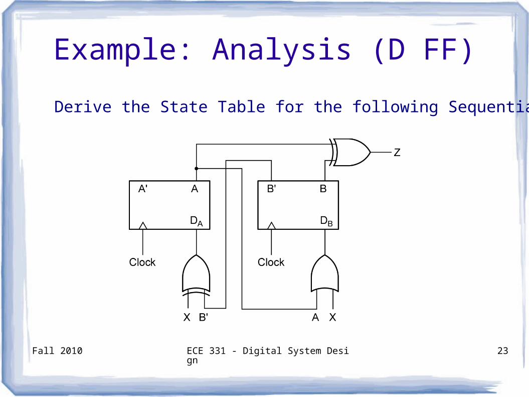
Example: Analysis (D FF)
Derive the State Table for the following Sequential Logic Circuit:

Fall 2010 ECE 331 - Digital System Design 24
Example: Analysis (D FF)
1. The flip-flop input equations and output equation are
DA = X xor B' DB = X or A Z = A or B
2. The next-state equations for the flip-flops are
A+ = X xor B' B+ = X or A

Fall 2010 ECE 331 - Digital System Design 25
Example: Analysis (D FF)
3. The corresponding next-state (K-) maps are

Fall 2010 ECE 331 - Digital System Design 26
Example: Analysis (D FF)
4. The state table, or transition table, is then determined from the next-state maps

Fall 2010 ECE 331 - Digital System Design 27
Example: Analysis (D FF)
5. The state graph can then be drawn from the state table

Fall 2010 ECE 331 - Digital System Design 28
Example:
Analyze a sequential circuit using JK Flip-Flops
Fall 2010 ECE 331 - Digital System Design 29
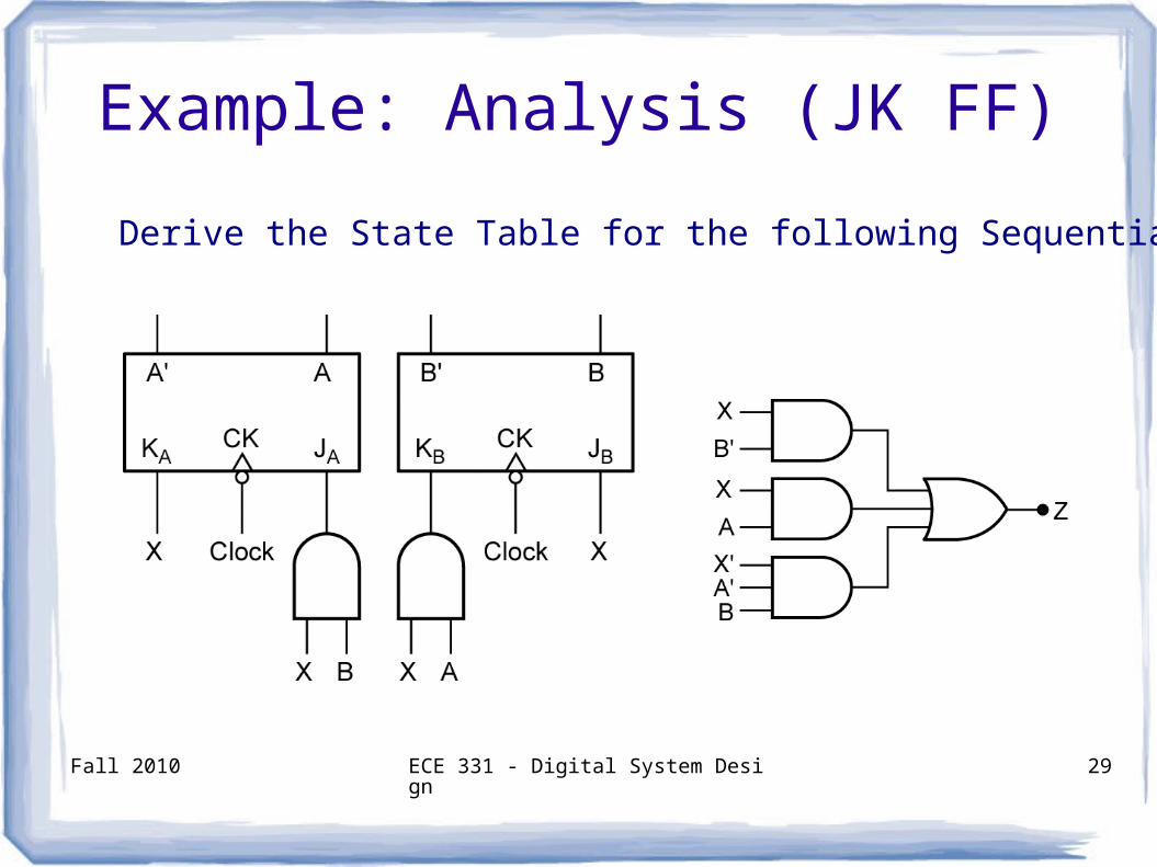
Example: Analysis (JK FF)
Derive the State Table for the following Sequential Logic Circuit:

Fall 2010 ECE 331 - Digital System Design 30
Example: Analysis (JK FF)
1. The flip-flop input equations and output equation are
JA = X.B JB = X Z = X.B' + X.A + X'.A'.B
2. The next-state equations for the flip-flops are
A+ = JA.A' + KA'.A B+ = JB.B' + KB'.B
KA = X KB = X.A
A+ = X.B.A' + X.A B+ = X.B' + X.A.B

Fall 2010 ECE 331 - Digital System Design 31
Example: Analysis (JK FF)
3. The corresponding next-state (K-) maps are

Fall 2010 ECE 331 - Digital System Design 32
Example: Analysis (JK FF)
4. The state table, and transition table, is then determined from the next-state maps

Fall 2010 ECE 331 - Digital System Design 33
Example: Analysis (JK FF)
5. The state graph can then be drawn from the state table

Fall 2010 ECE 331 - Digital System Design 34
Example:
Analyze a serial adder

Fall 2010 ECE 331 - Digital System Design 35
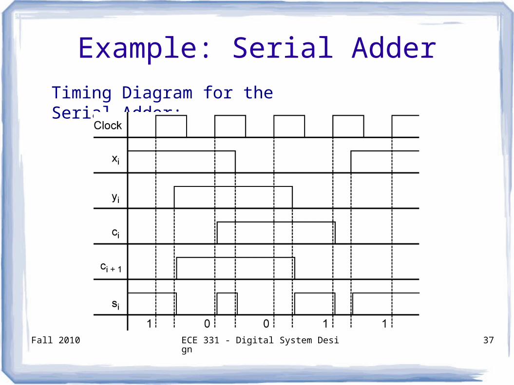
Example: Serial Adder
The serial adder adds two n-bit binary numbers.
serial inputs
serial output

Fall 2010 ECE 331 - Digital System Design 36
Example: Serial Adder
Truth Table for the Full Adder:
Fall 2010 ECE 331 - Digital System Design 37
Example: Serial Adder
Timing Diagram for the Serial Adder:

Fall 2010 ECE 331 - Digital System Design 38
Example: Serial Adder
State Graph for the Serial Adder:
What type of state machine is this?

Fall 2010 ECE 331 - Digital System Design 39
Example:
Analyze a state machine with multiple inputs.

Fall 2010 ECE 331 - Digital System Design 40
Example: Multiple Inputs
State Table for a state machine with multiple inputs:
Fall 2010 ECE 331 - Digital System Design 41
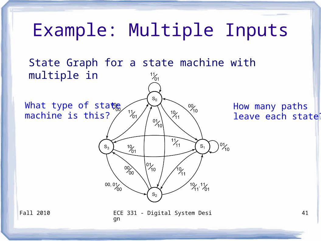
Example: Multiple Inputs
State Graph for a state machine with multiple inputs:
How many paths leave each state?
What type of statemachine is this?

Fall 2010 ECE 331 - Digital System Design 42
Questions?