Embed Size (px)
DESCRIPTION
ECE 545—Digital System Design with VHDL Lecture 1. Digital Logic Refresher Part B – Sequential Logic Building Blocks. Lecture Roadmap – Sequential Logic. Sequential Logic Building Blocks Flip-Flops, Latches Registers, Shift Registers Counters RAM. Textbook References. - PowerPoint PPT Presentation
Citation preview
1
ECE 545—Digital System Design with VHDLLecture 1
Digital Logic RefresherPart B – Sequential Logic Building Blocks
2
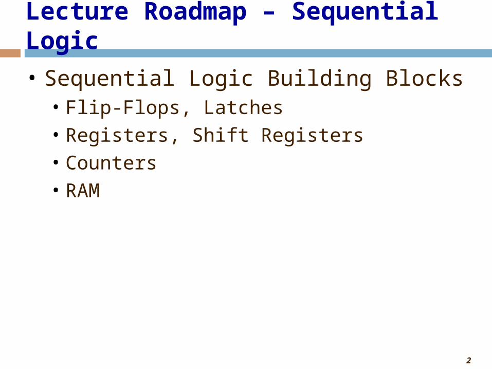
• Sequential Logic Building Blocks• Flip-Flops, Latches• Registers, Shift Registers• Counters• RAM
Lecture Roadmap – Sequential Logic
3
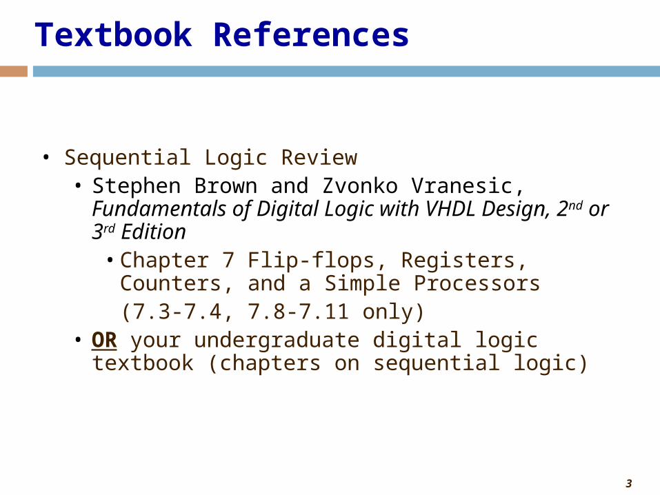
Textbook References
• Sequential Logic Review• Stephen Brown and Zvonko Vranesic, Fundamentals of Digital
Logic with VHDL Design, 2nd or 3rd Edition• Chapter 7 Flip-flops, Registers, Counters, and a Simple
Processors(7.3-7.4, 7.8-7.11 only)
• OR your undergraduate digital logic textbook (chapters on sequential logic)
4
Sequential Logic Building Blocks
some slides modified from:Brown and Vranesic, “Fundamentals of Digital Logic with VHDL Design, 2nd Edition”
S. Dandamudi, “Fundamentals of Computer Organization and Design”
5
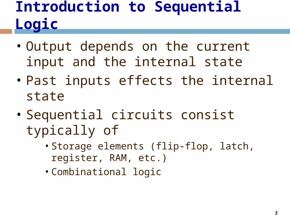
Introduction to Sequential Logic
• Output depends on the current input and the internal state
• Past inputs effects the internal state• Sequential circuits consist typically of
• Storage elements (flip-flop, latch, register, RAM, etc.)• Combinational logic
6
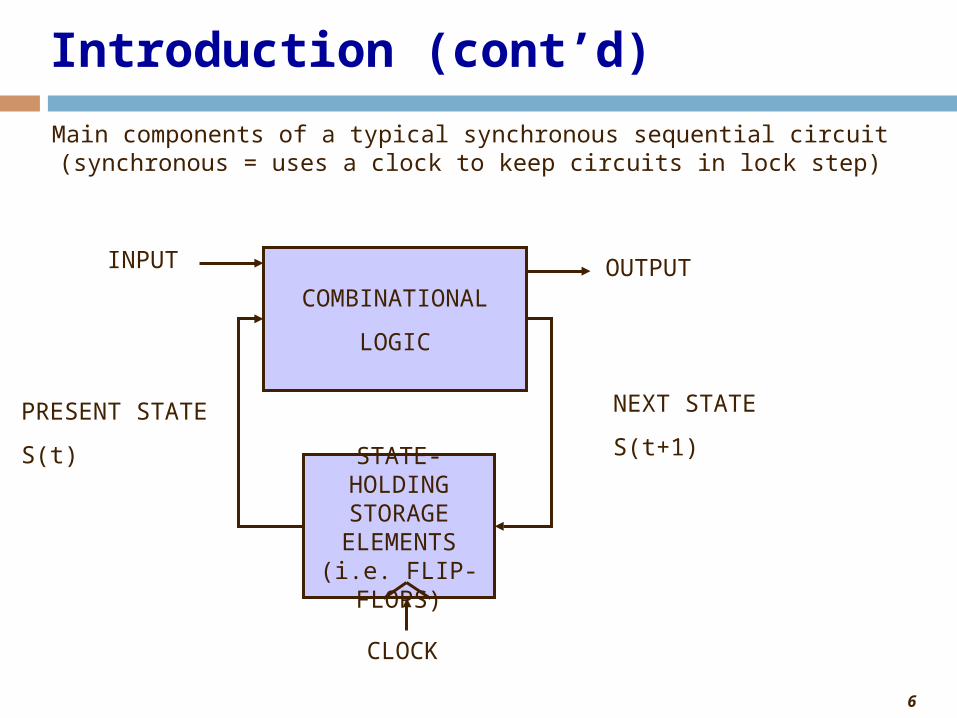
Introduction (cont’d)
Main components of a typical synchronous sequential circuit(synchronous = uses a clock to keep circuits in lock step)
COMBINATIONAL
LOGIC
STATE-HOLDING STORAGE ELEMENTS
(i.e. FLIP-FLOPS)
CLOCK
INPUT OUTPUT
NEXT STATE
S(t+1)PRESENT STATE
S(t)
7
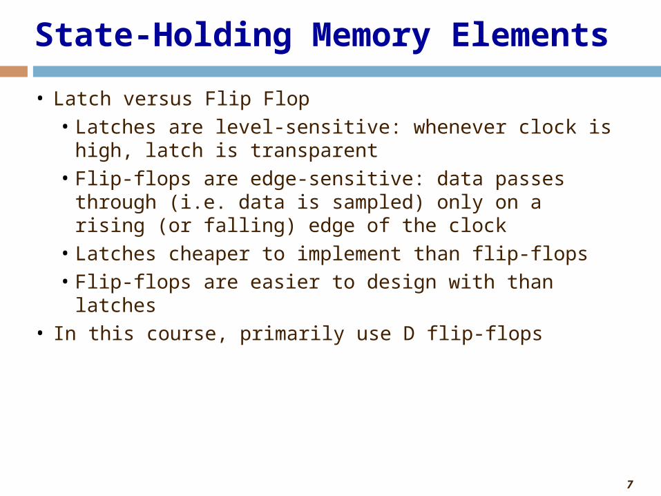
State-Holding Memory Elements
• Latch versus Flip Flop• Latches are level-sensitive: whenever clock is high, latch is
transparent• Flip-flops are edge-sensitive: data passes through (i.e. data
is sampled) only on a rising (or falling) edge of the clock• Latches cheaper to implement than flip-flops• Flip-flops are easier to design with than latches
• In this course, primarily use D flip-flops
8
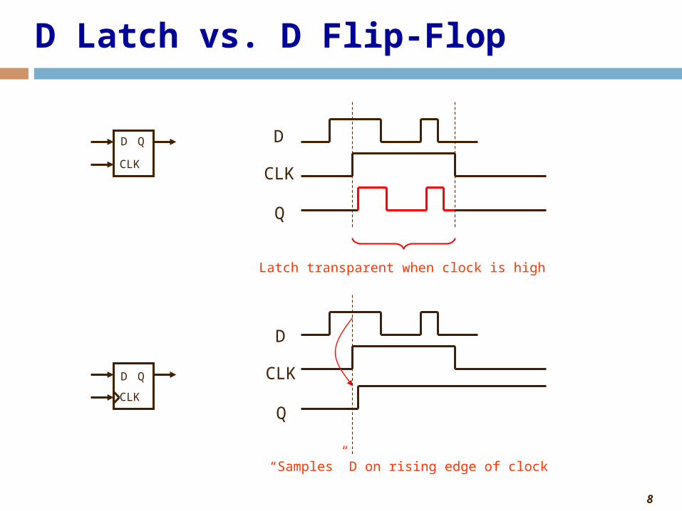
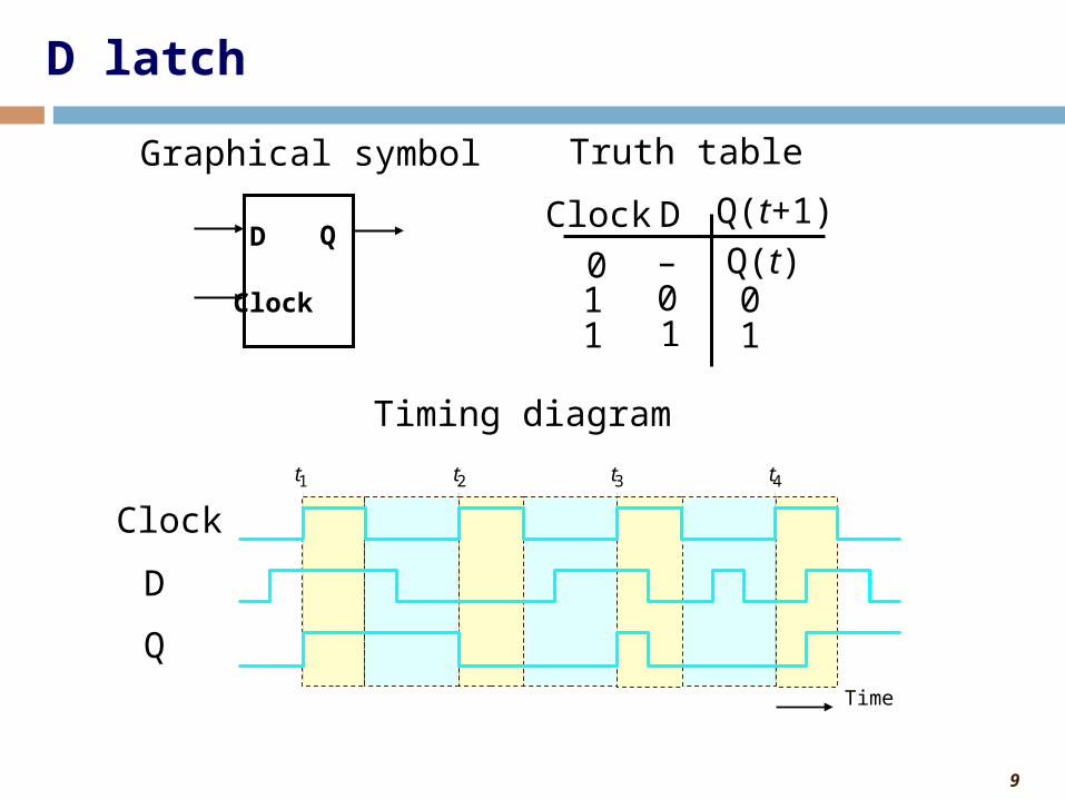
D Latch vs. D Flip-Flop
Latch transparent when clock is high
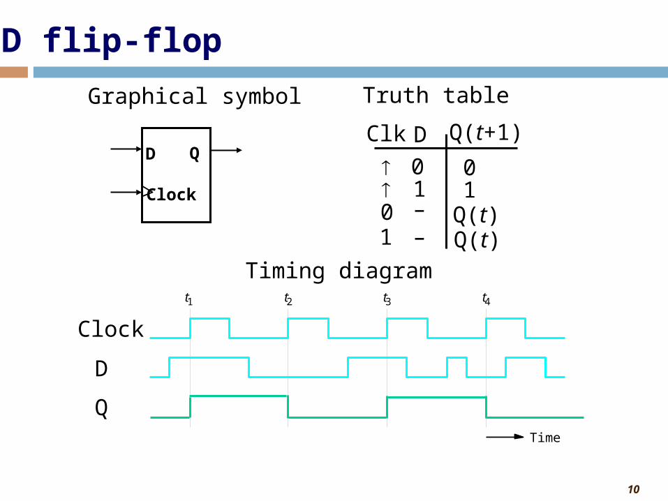
“Samples” D on rising edge of clock
D Q
CLK
D Q
CLK
D
CLK
Q
D
CLK
Q
9
Clock D 0 1 1
– 0 1
0 1
Truth table Graphical symbol
t 1 t 2 t 3 t 4
Time
Clock
D
Q
Timing diagram
Q(t+1)
Q(t)
D latch
D Q
Clock
10
Clk D
0 1
0 1
Truth table
t 1 t 2 t 3 t 4
Time
Clock
D
Q
Timing diagram
Q(t+1)
Q(t)
D flip-flop
D Q
Clock
Graphical symbol
0 – Q(t)1 –
11
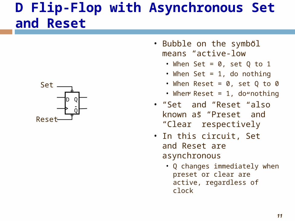
D Flip-Flop with Asynchronous Set and Reset
• Bubble on the symbol means “active-low”• When Set = 0, set Q to 1• When Set = 1, do nothing• When Reset = 0, set Q to 0 • When Reset = 1, do nothing
• “Set” and “Reset” also known as “Preset” and “Clear” respectively
• In this circuit, Set and Reset are asynchronous• Q changes immediately when
preset or clear are active, regardless of clock
D Q
Q
Set
Reset
12
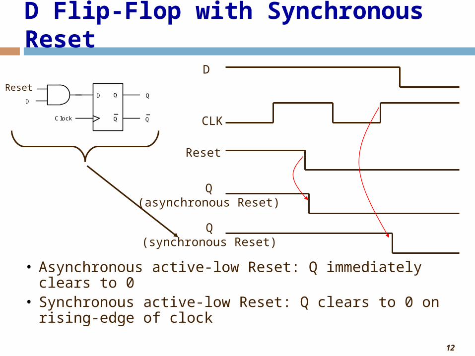
D Flip-Flop with Synchronous Reset
• Asynchronous active-low Reset: Q immediately clears to 0 • Synchronous active-low Reset: Q clears to 0 on rising-edge
of clock
D
Clock Q
QClear
D Q
Q
D
CLK
Reset
Q(asynchronous Reset)
Q(synchronous Reset)
Reset
13
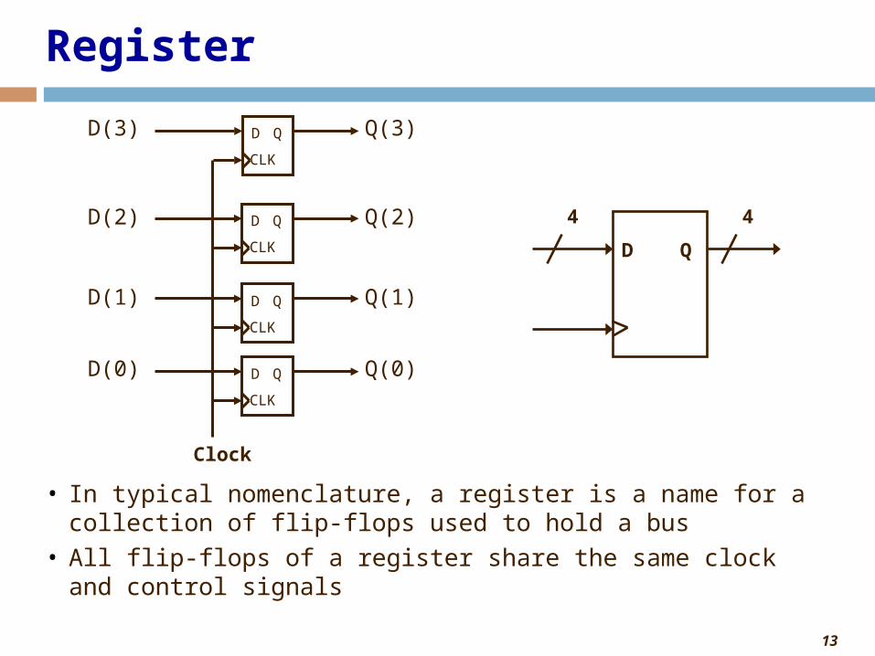
Register
• In typical nomenclature, a register is a name for a collection of flip-flops used to hold a bus
• All flip-flops of a register share the same clock and control signals
D Q
CLK
D Q
CLK
D Q
CLK
D Q
CLK
D(3)
D(2)
D(1)
D(0)
Q(3)
Q(2)
Q(1)
Q(0)
Clock
4 4
D Q
14
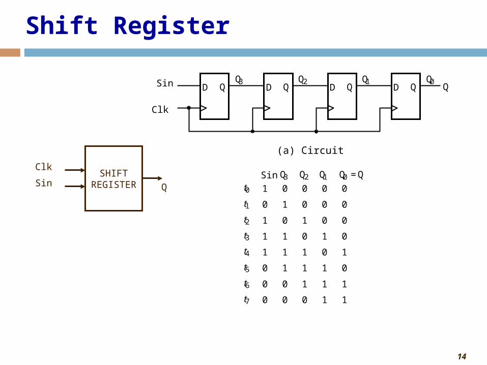
Shift Register
D Q
Clk
D Q
D Q D Q Sin Q
t 0
t 1
t 2
t 3
t 4
t 5
t 6
t 7
1
0
1
1
1
0
0
0
0
1
0
1
1
1
0
0
0
0
1
0
1
1
1
0
0
0
0
1
0
1
1
1
0
0
0
0
1
0
1
1
Q 3 Q 2 Q 1 Q 0 Q = Sin
(a) Circuit
Q 3 Q 2 Q 1 Q 0
SHIFTREGISTERSin
Clk
Q
15
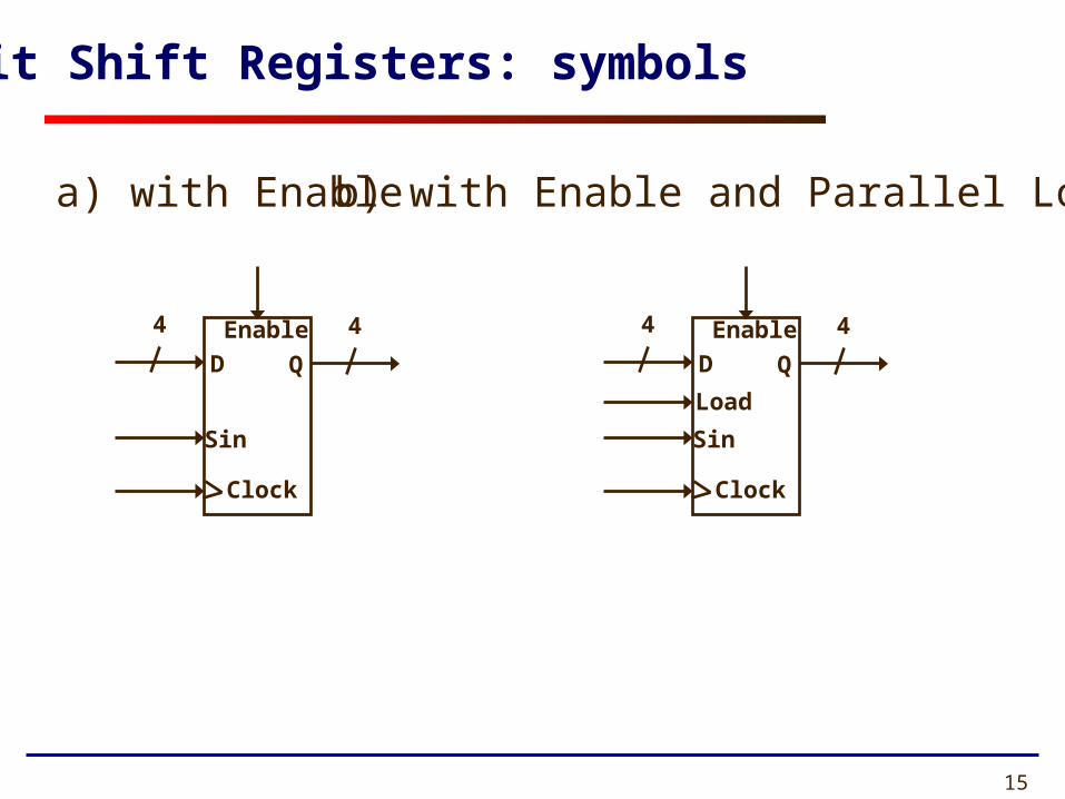
4-bit Shift Registers: symbols
Q
Enable
Clock
4
D
Sin
4
a) with Enable
Q
Enable
Clock
4
D
Load
Sin
4
b) with Enable and Parallel Load
16
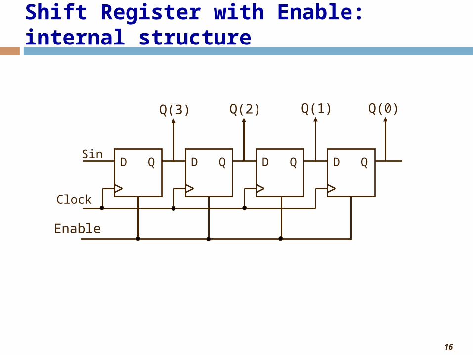
Shift Register with Enable: internal structure
D QSin
Clock
D Q D Q D Q
Q(3) Q(2) Q(1) Q(0)
Enable
17
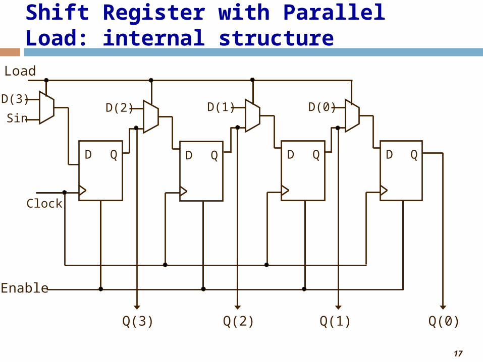
Shift Register with Parallel Load: internal structure
D(3)
D Q
Clock
Enable
SinD(2)
D Q
D(1)
D Q
D(0)
D Q
Q(0)Q(1)Q(2)Q(3)
Load
18
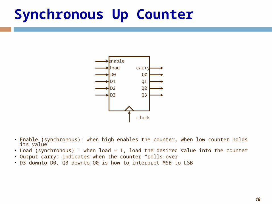
Synchronous Up Counter
• Enable (synchronous): when high enables the counter, when low counter holds its value• Load (synchronous) : when load = 1, load the desired value into the counter• Output carry: indicates when the counter “rolls over”• D3 downto D0, Q3 downto Q0 is how to interpret MSB to LSB
enableloadD0D1D2D3
Q0Q1Q2Q3
clock
carry
19
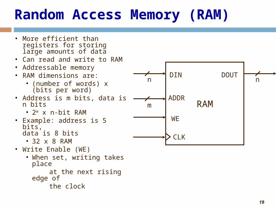
Random Access Memory (RAM)
• More efficient than registers for storing large amounts of data
• Can read and write to RAM• Addressable memory• RAM dimensions are:
• (number of words) x (bits per word)
• Address is m bits, data is n bits• 2m x n-bit RAM
• Example: address is 5 bits, data is 8 bits• 32 x 8 RAM
• Write Enable (WE)• When set, writing takes place at the next rising edge of the clock
RAM
DIN
ADDR
DOUT
WE
n n
m
CLK
20
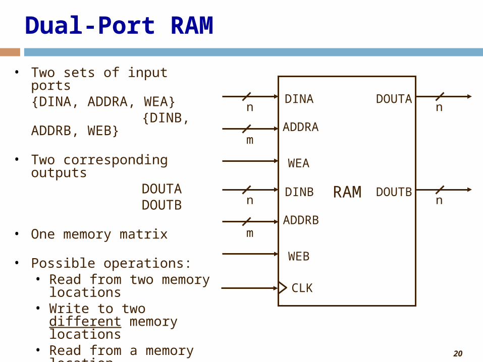
Dual-Port RAM
RAM
DINA
ADDRA
DOUTA
WEA
n n
m
CLK
DINB
ADDRB
DOUTB
WEB
n n
m
• Two sets of input ports{DINA, ADDRA, WEA}
{DINB, ADDRB, WEB}
• Two corresponding outputs DOUTA DOUTB
• One memory matrix
• Possible operations:• Read from two memory locations• Write to two different memory
locations• Read from a memory location and write to a memory location (different or the same)