Embed Size (px)
Citation preview
DIPLOMA IN ENGINEERING AND TECHNOLOGY
DEPARTMENT OF ELECTRONICS AND COMMUNICATION
SEMESTER PATTERN
IMPLEMENTED FROM 2020
CURRICULUM DEVELOPMENT CENTRE
DIRECTORATE OF TECHNICAL EDUCATION
CHENNAI
DIPLOMA IN ENGINEERING AND TECHNOLOGY
(1040,3040)
DEPARTMENT OF ELECTRONICS AND COMMUNICATION
ENGINEERING
SEMESTER PATTERN
N – SCHEME
IMPLEMENTED FROM 2020 - 2021
CURRICULUM DEVELOPMENT CENTRE
DIRECTORATE OF TECHNICAL EDUCATION
CHENNAI-600 025, TAMIL NADU
DIPLOMA IN ENGINEERING AND TECHNOLOGY
DEPARTMENT OF ELECTRONICS AND COMMUNICATION
DIRECTORATE OF TECHNICAL EDUCATION
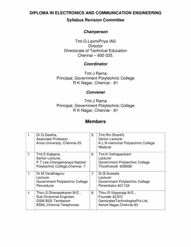
DIPLOMA IN ELECTRONICS AND COMMUNICATION ENGINEERING
Syllabus Revision Committee
Chairperson
Tmt.G.LaxmiPriya IAS
Director Directorate of Technical Education
Chennai – 600 025.
Coordinator
Tmt J Rama Principal, Government Polytechnic College
R K Nagar, Chennai - 81
Convener
Tmt J Rama Principal, Government Polytechnic College
R K Nagar, Chennai - 81
Members
1. Dr.G.Geetha, Associate Professor, Anna University, Chennai-25
5. Tmt.Rm.Shanthi, Senior Lecturer K.L.N memorial Polytechnic College Madurai
2. Tmt.E.Kalpana, Senior Lecturer, P.T.Lee.Chengalvaraya Naicker Polytechnic College,Chennai -7
6. Tmt.K.Vethapackiam Lecturer Government Polytechnic College Thoothukodi -628008
3. Dr.M.Varathaguru Lecturer Government Polytechnic College Perundurai
7. Dr.B.Suseela Lecturer Government Polytechnic College Perambalur-621104
4. Thiru.S.Dhanasekaran M.E., Sub-Divisional Engineer, GSM BSS Tambaram BSNL Chennai Telephones
8. Thiru.R.Vijayaraja M.E., Founder &CEO GemicatesTechnologiesPvt.Ltd., Ashok Nagar,Chennai-83
i
DIPLOMA COURSES IN ENGINEERING/TECHNOLOGY
(SEMESTER SYSTEM)
(Implemented from 2020 - 2021)
N – SCHEME
R E G U L A T I O N S*
*Applicable to the Diploma Courses other than Diploma in Hotel Management & Catering
Technology.
1. Description of the Course:
a. Full Time (3 years)
The Course for the Full Time Diploma in Engineering shall extend over a period of three
academic years, consisting of 6 semesters* and the First Year iscommon to all Engineering
Branches.
b. Sandwich (3½ years)
The Course for the Sandwich Diploma in Engineering shall extend over a period of three and
half academic years, consisting of 7 semesters* and the First Yearis common to all
Engineering Branches. The subjects of three years full timediploma course being regrouped
for academic convenience.
During 4th and/or during 7thsemester the students undergo industrial training forsix months/
one year. Industrial training examination will be conducted after completion of every 6
months of industrial training.
c. Part Time (4 years)
The course for the Part Time Diploma in Engineering shall extend over a period of 4
academic years containing of 8 semesters*, the subjects of 3 year full time diploma courses
being regrouped for academic convenience.
* Each Semester will have 16 weeks duration of study with 35 hrs. / Week for Regular
DiplomaCourses and 18 hrs. / Week for Part-Time Diploma Courses.
The Curriculum for all the 6 Semesters of Diploma courses (Engineering & Special Diploma
Coursesviz. Textile Technology, Leather Technology, Printing Technology, Chemical
Technology etc.) have been revised and revised curriculum is applicable for the candidates
admitted from 2020 – 2021 academic year onwards.
ii
2. Condition for Admission:
Condition for admission to the Diploma courses shall be required to have passed in the
S.S.L.C Examination of the Board of Secondary Education,Tamil Nadu.
(Or)
The Anglo Indian High School Examination with eligibility for Higher SecondaryCourse in
Tamil Nadu.
(Or)
The Matriculation Examination of Tamil Nadu.
(Or)
Any other Examinations recognized as equivalent to the above by the Board of
Secondary Education, Tamil Nadu.
Note: In addition, at the time of admission the candidate will have to satisfy certain minimum
requirements, which may be prescribed from time to time.
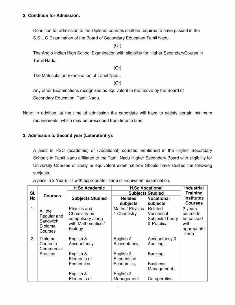
3. Admission to Second year (LateralEntry):
A pass in HSC (academic) or (vocational) courses mentioned in the Higher Secondary
Schools in Tamil Nadu affiliated to the Tamil Nadu Higher Secondary Board with eligibility for
University Courses of study or equivalent examination& Should have studied the following
subjects.
A pass in 2 Years ITI with appropriate Trade or Equivalent examination.
Sl. No
Courses
H.Sc Academic H.Sc Vocational Industrial Training Institutes Courses
Subjects Studied Subjects Studied
Related subjects
Vocational subjects
1. All the Regular and Sandwich Diploma Courses
Physics and Chemistry as compulsory along with Mathematics / Biology
Maths / Physics / Chemistry
Related Vocational SubjectsTheory& Practical
2 years course to be passed with appropriate Trade
2. Diploma Coursein Commercial Practice
English & Accountancy English & Elements of Economics English & Elements of
English & Accountancy, English & Elements of Economics, English & Management
Accountancy & Auditing, Banking, Business Management, Co-operative
-
iii
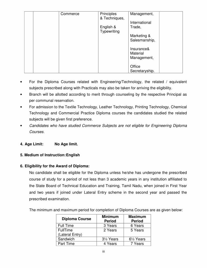
Commerce
Principles & Techniques, English & Typewriting
Management, International Trade, Marketing & Salesmanship, Insurance& Material Management, Office Secretaryship.
• For the Diploma Courses related with Engineering/Technology, the related / equivalent
subjects prescribed along with Practicals may also be taken for arriving the eligibility.
• Branch will be allotted according to merit through counseling by the respective Principal as
per communal reservation.
• For admission to the Textile Technology, Leather Technology, Printing Technology, Chemical
Technology and Commercial Practice Diploma courses the candidates studied the related
subjects will be given first preference.
• Candidates who have studied Commerce Subjects are not eligible for Engineering Diploma
Courses.
4. Age Limit: No Age limit.
5. Medium of Instruction: English
6. Eligibility for the Award of Diploma:
No candidate shall be eligible for the Diploma unless he/she has undergone the prescribed
course of study for a period of not less than 3 academic years in any institution affiliated to
the State Board of Technical Education and Training, Tamil Nadu, when joined in First Year
and two years if joined under Lateral Entry scheme in the second year and passed the
prescribed examination.
The minimum and maximum period for completion of Diploma Courses are as given below:
Diploma Course Minimum
Period Maximum
Period Full Time 3 Years 6 Years FullTime (Lateral Entry)
2 Years 5 Years
Sandwich 3½ Years 6½ Years Part Time 4 Years 7 Years
iv
This will come into effect from N Scheme onwards i.e. from the academic year 2020-2021.
7. Subjects of Study and Curriculum outline:
The subjects of study shall be in accordance with the syllabus prescribed from time to time,
both in theory and practical subjects.
The curriculum outline is given in Annexure – I.
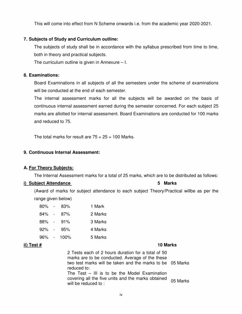
8. Examinations:
Board Examinations in all subjects of all the semesters under the scheme of examinations
will be conducted at the end of each semester.
The internal assessment marks for all the subjects will be awarded on the basis of
continuous internal assessment earned during the semester concerned. For each subject 25
marks are allotted for internal assessment. Board Examinations are conducted for 100 marks
and reduced to 75.
The total marks for result are 75 + 25 = 100 Marks.
9. Continuous Internal Assessment:
A. For Theory Subjects:
The Internal Assessment marks for a total of 25 marks, which are to be distributed as follows:
i) Subject Attendance 5 Marks
(Award of marks for subject attendance to each subject Theory/Practical willbe as per the
range given below)
80% - 83% 1 Mark
84% - 87% 2 Marks
88% - 91% 3 Marks
92% - 95% 4 Marks
96% - 100% 5 Marks
ii) Test # 10 Marks
2 Tests each of 2 hours duration for a total of 50 marks are to be conducted. Average of the these two test marks will be taken and the marks to be reduced to:
05 Marks
The Test – III is to be the Model Examination covering all the five units and the marks obtained will be reduced to :
05 Marks
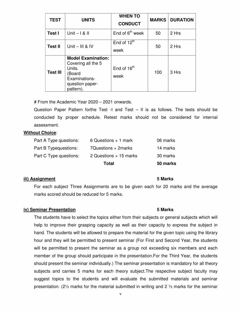
v
TEST UNITS WHEN TO
CONDUCT MARKS DURATION
Test I Unit – I & II End of 6th week 50 2 Hrs
Test II Unit – III & IV End of 12th
week 50 2 Hrs
Test III
Model Examination: Covering all the 5 Units. (Board Examinations-question paper-pattern).
End of 16th
week 100 3 Hrs
# From the Academic Year 2020 – 2021 onwards.
Question Paper Pattern forthe Test -I and Test – II is as follows. The tests should be
conducted by proper schedule. Retest marks should not be considered for internal
assessment.
Without Choice:
Part A Type questions: 6 Questions × 1 mark 06 marks
Part B Typequestions: 7Questions × 2marks 14 marks
Part C Type questions: 2 Questions × 15 marks 30 marks
Total 50 marks
iii) Assignment 5 Marks
For each subject Three Assignments are to be given each for 20 marks and the average
marks scored should be reduced for 5 marks.
iv) Seminar Presentation 5 Marks
The students have to select the topics either from their subjects or general subjects which will
help to improve their grasping capacity as well as their capacity to express the subject in
hand. The students will be allowed to prepare the material for the given topic using the library
hour and they will be permitted to present seminar (For First and Second Year, the students
will be permitted to present the seminar as a group not exceeding six members and each
member of the group should participate in the presentation.For the Third Year, the students
should present the seminar individually.) The seminar presentation is mandatory for all theory
subjects and carries 5 marks for each theory subject.The respective subject faculty may
suggest topics to the students and will evaluate the submitted materials and seminar
presentation. (2½ marks for the material submitted in writing and 2 ½ marks for the seminar
vi
presentation). For each subject minimum of two seminars are to be given and the average
marks scored should be reduced to 5 marks.
All Test Papers, Assignment Papers / Notebooks and the seminar presentation written
material after getting the signature with date from the students must be kept in safe custody
in the department for verification and audit. It should be preserved for onesemester after
publication of Board Exam results and produced to the flying squad and the inspection team
at the time of inspection/verification.
B. For Practical Subjects:
The Internal Assessmentmark for a total of 25 marks which are to be distributed as follows:-
a) Attendance :5Marks
(Award of marks same as theory subjects)
b) Procedure/ observation and tabulation/
Other Practical related Work :10Marks
c) Record writing :10Marks
TOTAL : 25Marks
• All the Experiments/Exercises indicated in the syllabus should be completed and the same to
be given for final Board examinations.
• The observation note book / manual should be maintained for 10 marks. The observation
note book / manual withsketches, circuits, programme, reading and calculation written by the
students manually depends upon the practical subject during practical classes should be
evaluated properly during the practical class hours with date.
• The Record work for every completed exercise should be submitted in the subsequent
practical classes and marks should be awarded for 10 marks for each exercise as per the
above allocation.
• At the end of the Semester, the average marks of all the exercises should be calculated for
20 marks (including Observation and Record writing) and the marks awarded for attendance
is to be added to arrive at the internal assessment mark for Practical. (20+5=25 marks)
• Only regular students, appearing first time have to submit the duly signed bonafiderecord
note book/file during the Practical Board Examinations.
All the marks awarded for Assignments, Tests, Seminar presentation and Attendance should be
entered periodically in the Personal Theory Log Book of the staff, who is handling the theory
subject.
The marks awarded for Observation, Record work and Attendance should be entered
periodically in the Personal Practical Log Book of the staff, who is handling the practical subject.
vii
10. Communication Skill Practical, Computer ApplicationPractical and Physical
Education:
The Communication Skill Practical and Computer Application Practical with more emphasis
are being introduced in First Year. Much Stress is given to increase the Communication skill
and ICT skill of students.
As per the recommendation of MHRD and under Fit India scheme, the Physical education is
introduced to encourage students to remain healthy and fit by including physical activities
and sports.
11. Project Work and Internship:
The students of all the Diploma Courseshave to do a Project Work as part of the Curriculum
and in partial fulfillment for the award of Diploma by the State Board of Technical Education
and Training, Tamil Nadu. In order to encourage students to do worthwhile and innovative
projects, every year prizes are awarded for the best three projects i.e. institution wise, region
wise and state wise. The Project work must be reviewed twice in the samesemester.
The project work is approved during the V semester by the properly constituted
committee with guidelines.
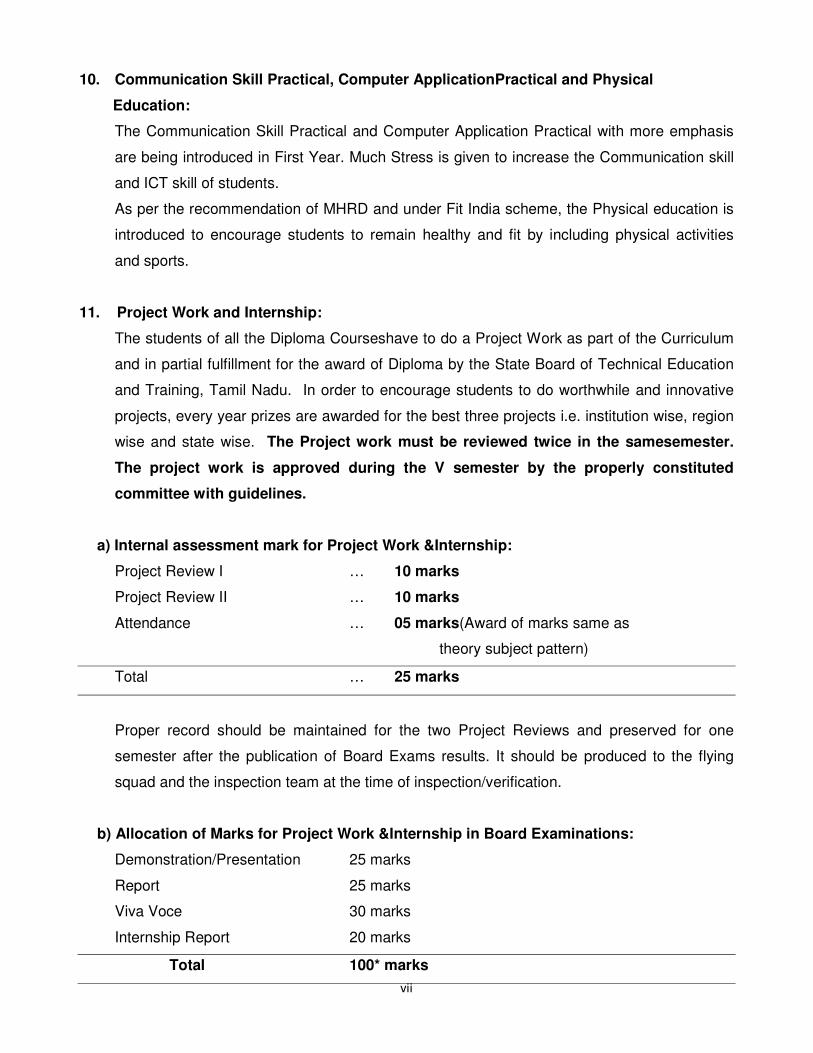
a) Internal assessment mark for Project Work &Internship:
Project Review I … 10 marks
Project Review II … 10 marks
Attendance … 05 marks(Award of marks same as
theory subject pattern)
Total … 25 marks
Proper record should be maintained for the two Project Reviews and preserved for one
semester after the publication of Board Exams results. It should be produced to the flying
squad and the inspection team at the time of inspection/verification.
b) Allocation of Marks for Project Work &Internship in Board Examinations:
Demonstration/Presentation 25 marks
Report 25 marks
Viva Voce 30 marks
Internship Report 20 marks
Total 100* marks
viii
*Examination will be conducted for 100 marks and will be converted to 75 marks.
c) Internship Report:
The internship training for a period of two weeks shall be undergone by every candidate at
the end of IV / V semester during vacation. The certificate shall be produced along with the
internship report for evaluation. The evaluation of internship training shall be done along with
final year “Project Work & Internship” for 20 marks. The internship shall be undertaken in any
industry / Government or Private certified agencies which are in social sector / Govt. Skill
Centres / Institutions / Schemes.
A neatly prepared PROJECT REPORT as per the format has to be submitted by
individualstudent during the Project Work &Internship Board examination.
12.Scheme of Examinations:
The Scheme of examinations for subjects is given in Annexure - II.
13.Criteria for Pass:
1. No candidate shall be eligible for the award of Diploma unless he/she has undergone the
prescribed course of study successfully in an institution approved by AICTE and affiliated to
the State Board of Technical Education & Training, Tamil Nadu and pass all the subjects
prescribed in the curriculum.
2. A candidate shall be declared to have passed the examination in a subject if he/she secures
not less than 40% in theory subjects and 50% in practical subjects out of the total prescribed
maximum marks including both the Internal Assessment and the Board Examinations marks
put together, subject to the condition that he/she secures at least a minimum of 40 marks out
of 100 marks in the Board Theory Examinations and a minimum of 50 marks out of 100
marks in the Board Practical Examinations.
14. Classification of successful candidates:
Classification of candidates who will pass out the final examinations fromApril 2023 onwards
(Joined first year in 2020 -2021) will be done as specified below.
ix
First Class with Superlative Distinction:
A candidate will be declared to have passed in First Class with Superlative Distinction if
he/she secures not less than 75% of the marks in all the subjects and passes all the
semesters in the first appearance itself and passes all subjects within the stipulated period of
study 2 / 3/ 3½/ 4 years [Full time(lateral entry)/Full Time/Sandwich/Part Time] without any
break in study.
First Class with Distinction:
A candidate will be declared to have passed in First Class with Distinction if he/she
secures not less than 75% of the aggregate marks in all the semesters put together and
passes all the semesters except the I and II semester in the first appearance itself and
passes all subjects within the stipulated period of study 2 / 3/ 3½/ 4 years [Full time(lateral
entry)/Full Time/Sandwich/Part Time] without any break in study.
First Class:
A candidate will be declared to have passed in First Class if he/she secures not less than
60% of the aggregate marks in all the semesters put together and passes all the subjects
within the stipulated period of study 2 / 3/ 3½/ 4 years [Full time(lateral entry)/Full
Time/Sandwich/Part Time] without any break in study.
Second Class:
All other successful candidates will be declared to have passed in Second Class.
The above classifications are also applicable for the Sandwich / Part-Time students who
pass out Final Examination from October 2023 /April 2024 onwards (both joined First Year in
2020 -2021)
15. Duration of a period in the Class Time Table:
The duration of each period of instruction is1 hour and the total period of instruction hours
excluding interval and lunch break in a day should be uniformly maintained as 7 hours
corresponding to 7 periods of instruction (Theory & Practical).
******
BLANK PAGE
1
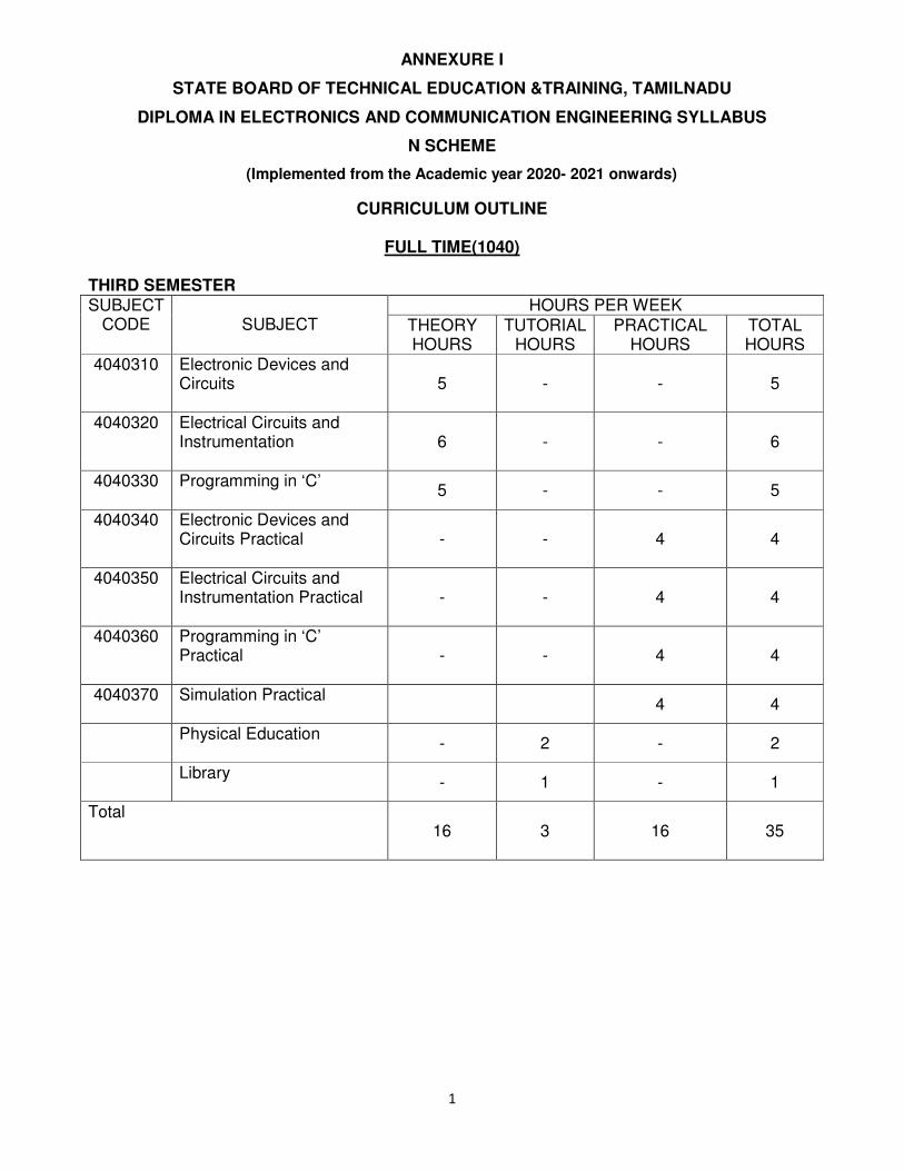
ANNEXURE I
STATE BOARD OF TECHNICAL EDUCATION &TRAINING, TAMILNADU
DIPLOMA IN ELECTRONICS AND COMMUNICATION ENGINEERING SYLLABUS
N SCHEME
(Implemented from the Academic year 2020- 2021 onwards)
CURRICULUM OUTLINE
FULL TIME(1040)
THIRD SEMESTER SUBJECT
CODE
SUBJECT
HOURS PER WEEK
THEORY HOURS
TUTORIAL HOURS
PRACTICAL HOURS
TOTAL HOURS
4040310 Electronic Devices and Circuits
5 - - 5
4040320 Electrical Circuits and Instrumentation
6 - - 6
4040330 Programming in ‘C’
5 - - 5
4040340 Electronic Devices and Circuits Practical
- - 4 4
4040350 Electrical Circuits and Instrumentation Practical
- - 4 4
4040360 Programming in ‘C’ Practical
- - 4 4
4040370 Simulation Practical
4 4
Physical Education
- 2 - 2
Library
- 1 - 1
Total 16
3
16 35
2
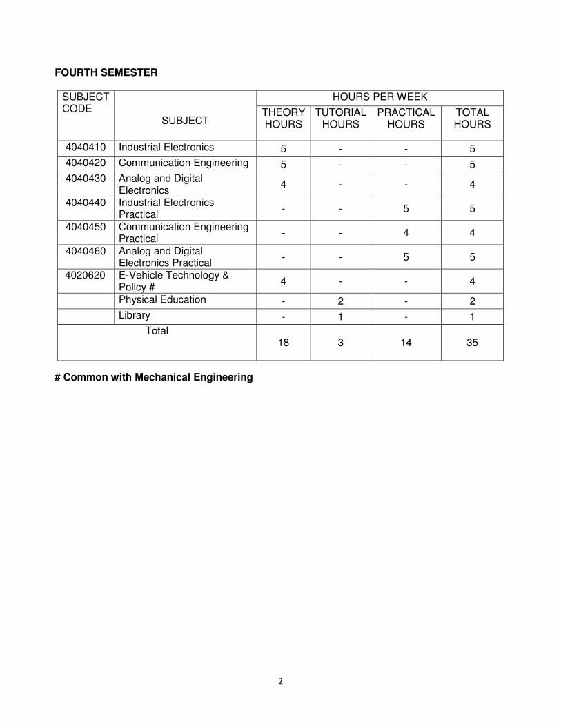
FOURTH SEMESTER
SUBJECT CODE
SUBJECT
HOURS PER WEEK
THEORY HOURS
TUTORIAL HOURS
PRACTICAL HOURS
TOTAL HOURS
4040410 Industrial Electronics 5 - - 5
4040420 Communication Engineering 5 - - 5
4040430 Analog and Digital Electronics
4 - - 4
4040440 Industrial Electronics Practical
- - 5 5
4040450 Communication Engineering Practical
- - 4 4
4040460 Analog and Digital Electronics Practical
- - 5 5
4020620 E-Vehicle Technology & Policy #
4 - - 4
Physical Education - 2 - 2
Library - 1 - 1
Total 18
3
14 35
# Common with Mechanical Engineering
3
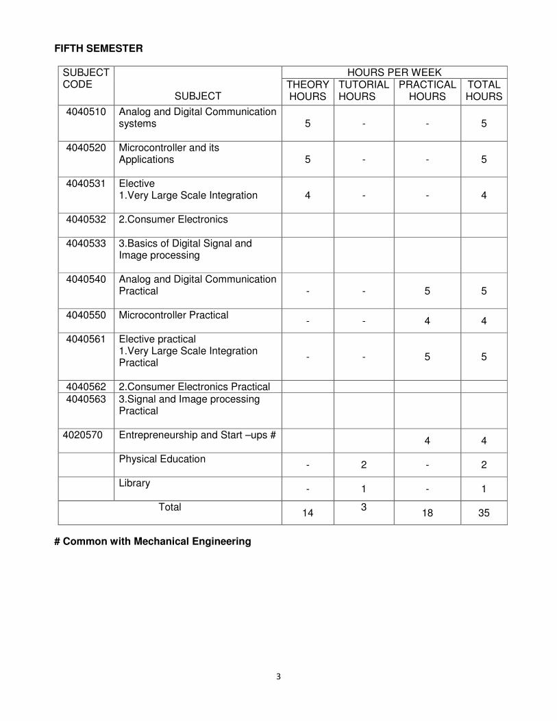
FIFTH SEMESTER
SUBJECT CODE
SUBJECT
HOURS PER WEEK THEORY HOURS
TUTORIAL HOURS
PRACTICAL HOURS
TOTAL HOURS
4040510 Analog and Digital Communication systems
5 - - 5
4040520 Microcontroller and its Applications
5 - - 5
4040531 Elective 1.Very Large Scale Integration
4 - - 4
4040532 2.Consumer Electronics
4040533 3.Basics of Digital Signal and Image processing
4040540 Analog and Digital Communication Practical
- - 5 5
4040550 Microcontroller Practical
- - 4 4
4040561 Elective practical 1.Very Large Scale Integration Practical
- - 5 5
4040562 2.Consumer Electronics Practical
4040563 3.Signal and Image processing Practical
4020570 Entrepreneurship and Start –ups #
4 4
Physical Education
- 2 - 2
Library
- 1 - 1
Total 14
3
18 35
# Common with Mechanical Engineering
4
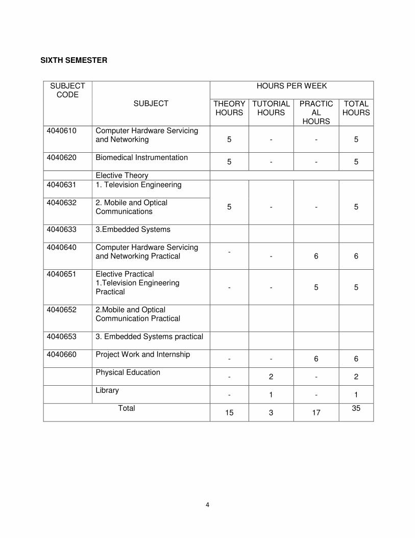
SIXTH SEMESTER
SUBJECT
CODE
SUBJECT
HOURS PER WEEK
THEORY HOURS
TUTORIAL HOURS
PRACTICAL
HOURS
TOTAL HOURS
4040610 Computer Hardware Servicing and Networking
5 - - 5
4040620 Biomedical Instrumentation
5 - - 5
Elective Theory
4040631 1. Television Engineering
5
-
-
5
4040632 2. Mobile and Optical Communications
4040633 3.Embedded Systems
4040640 Computer Hardware Servicing and Networking Practical
-
- 6 6
4040651 Elective Practical 1.Television Engineering Practical
- - 5 5
4040652 2.Mobile and Optical Communication Practical
4040653 3. Embedded Systems practical
4040660 Project Work and Internship
- - 6 6
Physical Education
- 2 - 2
Library
- 1 - 1
Total 15 3 17
35
5
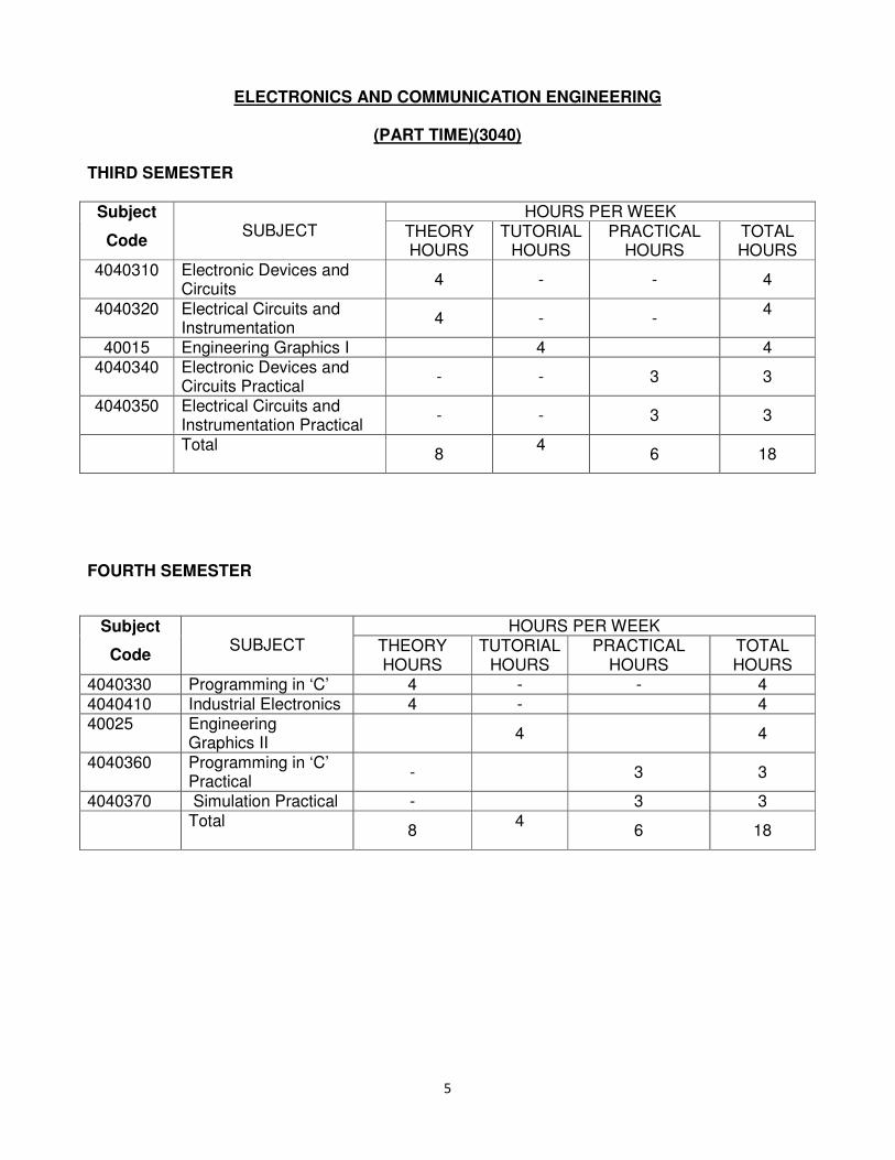
ELECTRONICS AND COMMUNICATION ENGINEERING
(PART TIME)(3040)
THIRD SEMESTER
Subject
Code
SUBJECT
HOURS PER WEEK THEORY HOURS
TUTORIAL HOURS
PRACTICAL HOURS
TOTAL HOURS
4040310 Electronic Devices and Circuits
4 - - 4
4040320 Electrical Circuits and Instrumentation
4 - - 4
40015 Engineering Graphics I 4 4 4040340 Electronic Devices and
Circuits Practical - - 3 3
4040350 Electrical Circuits and Instrumentation Practical
- - 3 3
Total 8
4
6 18
FOURTH SEMESTER
Subject
Code
SUBJECT
HOURS PER WEEK THEORY HOURS
TUTORIAL HOURS
PRACTICAL HOURS
TOTAL HOURS
4040330 Programming in ‘C’ 4 - - 4 4040410 Industrial Electronics 4 - 4 40025 Engineering
Graphics II 4 4
4040360 Programming in ‘C’ Practical
- 3 3
4040370 Simulation Practical - 3 3 Total
8 4
6 18
6
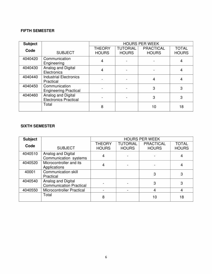
FIFTH SEMESTER
Subject
Code
SUBJECT
HOURS PER WEEK THEORY HOURS
TUTORIAL HOURS
PRACTICAL HOURS
TOTAL HOURS
4040420 Communication Engineering
4 - - 4
4040430 Analog and Digital Electronics
4 - - 4
4040440 Industrial Electronics Practical
- - 4 4
4040450 Communication Engineering Practical
- - 3 3
4040460 Analog and Digital Electronics Practical
- - 3 3
Total 8
10 18
SIXTH SEMESTER
Subject
Code
SUBJECT
HOURS PER WEEK THEORY HOURS
TUTORIAL HOURS
PRACTICAL HOURS
TOTAL HOURS
4040510 Analog and Digital Communication systems
4 - - 4
4040520 Microcontroller and its Applications
4 - - 4
40001 Communication skill Practical
3 3
4040540 Analog and Digital Communication Practical
- - 3 3
4040550 Microcontroller Practical - - 4 4 Total
8
10 18
7
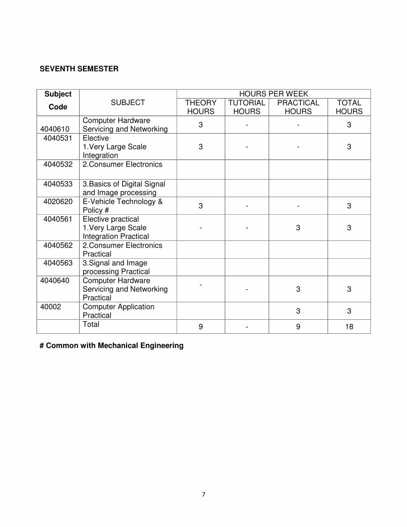
SEVENTH SEMESTER
Subject
Code
SUBJECT
HOURS PER WEEK THEORY HOURS
TUTORIAL HOURS
PRACTICAL HOURS
TOTAL HOURS
4040610
Computer Hardware Servicing and Networking
3 - - 3
4040531 Elective 1.Very Large Scale Integration
3 - - 3
4040532 2.Consumer Electronics
4040533 3.Basics of Digital Signal and Image processing
4020620 E-Vehicle Technology & Policy #
3 - - 3
4040561 Elective practical 1.Very Large Scale Integration Practical
- - 3 3
4040562 2.Consumer Electronics Practical
4040563 3.Signal and Image processing Practical
4040640 Computer Hardware Servicing and Networking Practical
-
- 3 3
40002 Computer Application Practical
3 3
Total 9 - 9 18
# Common with Mechanical Engineering
8
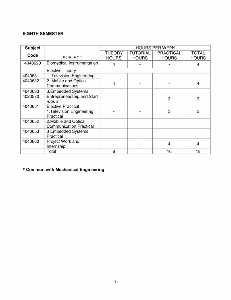
EIGHTH SEMESTER
Subject
Code
SUBJECT
HOURS PER WEEK
THEORY HOURS
TUTORIAL HOURS
PRACTICAL HOURS
TOTAL HOURS
4040620 Biomedical Instrumentation 4 - - 4
Elective Theory
4040631 1. Television Engineering 4
-
-
4
4040632 2. Mobile and Optical Communications
4040633 3.Embedded Systems
4020570 Entrepreneurship and Start -ups #
3 3
4040651 Elective Practical 1.Television Engineering Practical
- - 3 3
4040652 2.Mobile and Optical Communication Practical
4040653 3 Embedded Systems Practical
4040660 Project Work and Internship
- - 4 4
Total 8 10 18
# Common with Mechanical Engineering
9
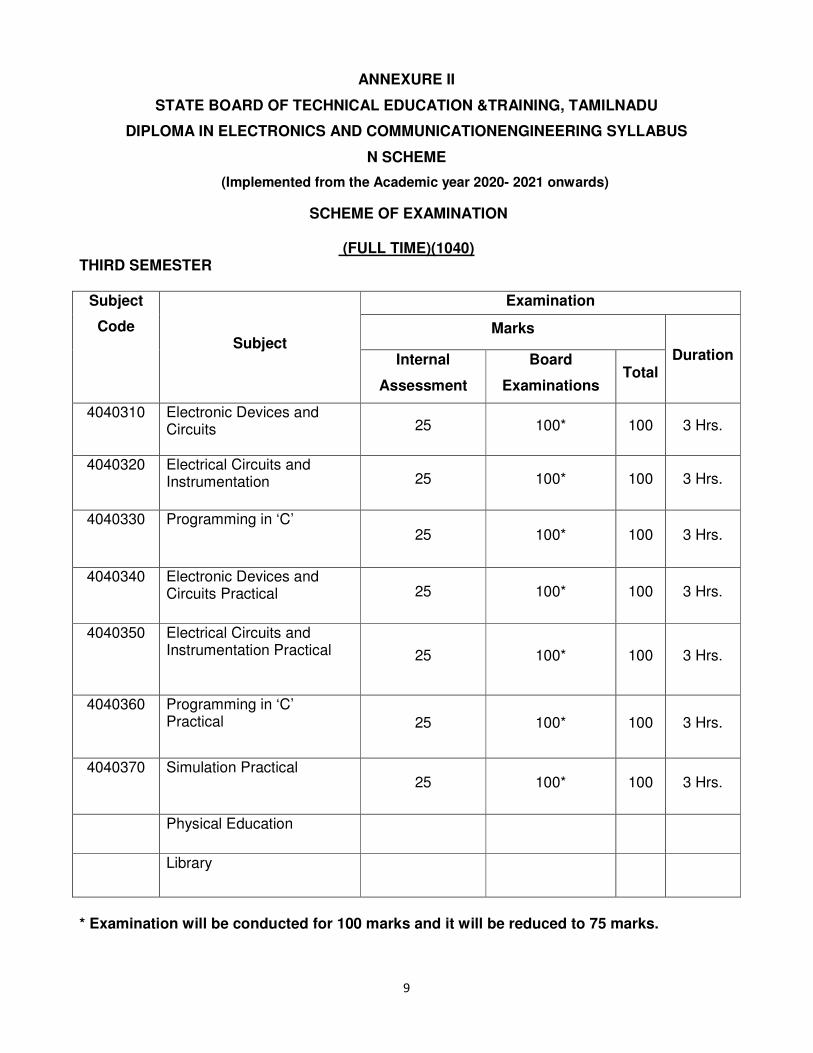
ANNEXURE II
STATE BOARD OF TECHNICAL EDUCATION &TRAINING, TAMILNADU
DIPLOMA IN ELECTRONICS AND COMMUNICATIONENGINEERING SYLLABUS
N SCHEME
(Implemented from the Academic year 2020- 2021 onwards)
SCHEME OF EXAMINATION
(FULL TIME)(1040) THIRD SEMESTER
Subject
Code Subject
Examination
Marks
Duration Internal
Assessment
Board
Examinations Total
4040310 Electronic Devices and Circuits
25 100* 100 3 Hrs.
4040320 Electrical Circuits and Instrumentation
25 100* 100 3 Hrs.
4040330 Programming in ‘C’ 25 100* 100 3 Hrs.
4040340 Electronic Devices and Circuits Practical
25 100* 100 3 Hrs.
4040350 Electrical Circuits and Instrumentation Practical
25 100* 100 3 Hrs.
4040360 Programming in ‘C’ Practical
25 100* 100 3 Hrs.
4040370 Simulation Practical 25 100* 100 3 Hrs.
Physical Education
Library
* Examination will be conducted for 100 marks and it will be reduced to 75 marks.
10
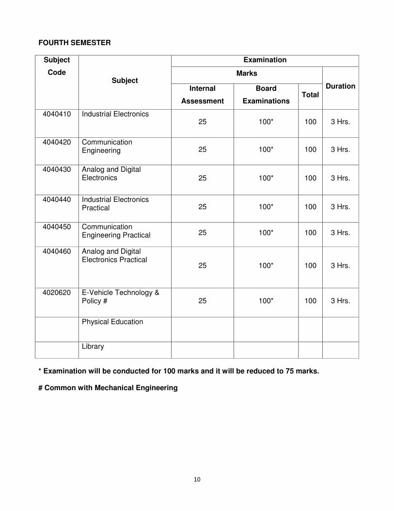
FOURTH SEMESTER
Subject
Code Subject
Examination
Marks
Duration Internal
Assessment
Board
Examinations Total
4040410 Industrial Electronics 25 100* 100 3 Hrs.
4040420 Communication Engineering 25 100* 100 3 Hrs.
4040430 Analog and Digital Electronics 25 100* 100 3 Hrs.
4040440 Industrial Electronics Practical 25 100* 100 3 Hrs.
4040450 Communication Engineering Practical 25 100* 100 3 Hrs.
4040460 Analog and Digital Electronics Practical
25 100* 100 3 Hrs.
4020620 E-Vehicle Technology & Policy # 25 100* 100 3 Hrs.
Physical Education
Library
* Examination will be conducted for 100 marks and it will be reduced to 75 marks. # Common with Mechanical Engineering
11
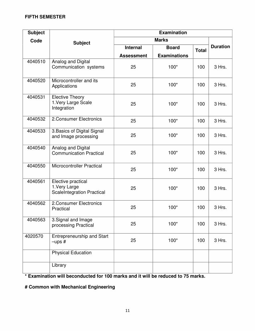
FIFTH SEMESTER
Subject
Code Subject
Examination
Marks
Duration Internal
Assessment
Board
Examinations Total
4040510 Analog and Digital Communication systems
25 100* 100 3 Hrs.
4040520 Microcontroller and its Applications
25 100* 100 3 Hrs.
4040531 Elective Theory 1.Very Large Scale Integration
25 100* 100 3 Hrs.
4040532 2.Consumer Electronics
25 100* 100 3 Hrs.
4040533 3.Basics of Digital Signal and Image processing
25 100* 100 3 Hrs.
4040540 Analog and Digital Communication Practical
25 100* 100 3 Hrs.
4040550 Microcontroller Practical 25 100* 100 3 Hrs.
4040561 Elective practical 1.Very Large ScaleIntegration Practical
25 100* 100 3 Hrs.
4040562 2.Consumer Electronics Practical
25 100* 100 3 Hrs.
4040563 3.Signal and Image processing Practical
25 100* 100 3 Hrs.
4020570 Entrepreneurship and Start –ups #
25 100* 100 3 Hrs.
Physical Education
Library
* Examination will beconducted for 100 marks and it will be reduced to 75 marks. # Common with Mechanical Engineering
12
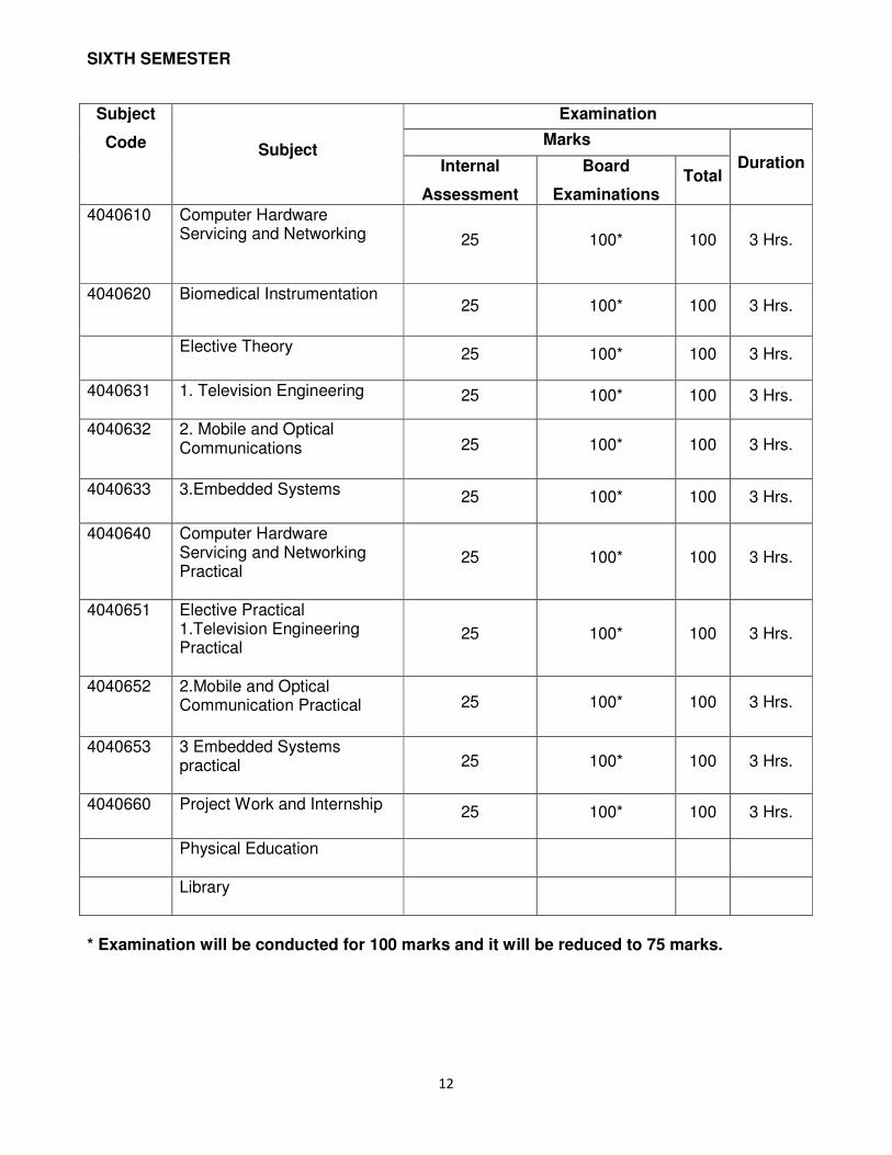
SIXTH SEMESTER
Subject
Code Subject
Examination
Marks
Duration Internal
Assessment
Board
Examinations Total
4040610 Computer Hardware Servicing and Networking
25 100* 100 3 Hrs.
4040620 Biomedical Instrumentation 25 100* 100 3 Hrs.
Elective Theory 25 100* 100 3 Hrs.
4040631 1. Television Engineering
25 100* 100 3 Hrs.
4040632 2. Mobile and Optical Communications
25 100* 100 3 Hrs.
4040633 3.Embedded Systems
25 100* 100 3 Hrs.
4040640 Computer Hardware Servicing and Networking Practical
25 100* 100 3 Hrs.
4040651 Elective Practical 1.Television Engineering Practical
25 100* 100 3 Hrs.
4040652 2.Mobile and Optical Communication Practical
25 100* 100 3 Hrs.
4040653 3 Embedded Systems practical
25 100* 100 3 Hrs.
4040660 Project Work and Internship
25 100* 100 3 Hrs.
Physical Education
Library
* Examination will be conducted for 100 marks and it will be reduced to 75 marks.
13
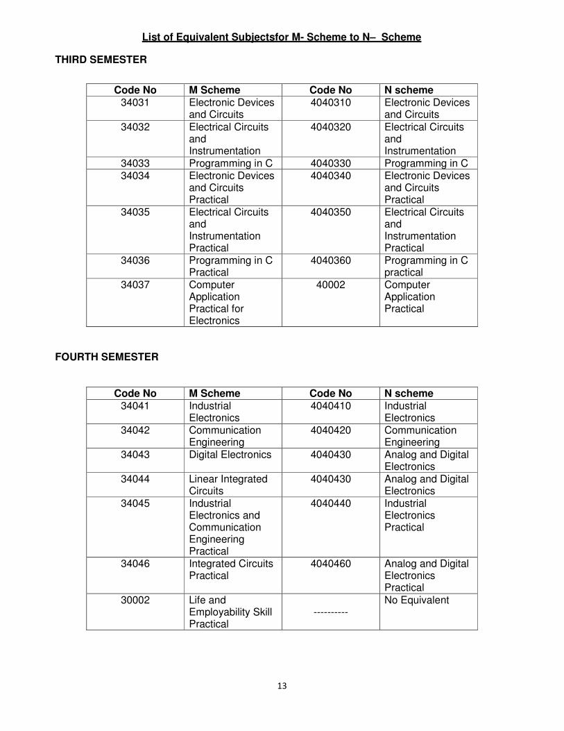
List of Equivalent Subjectsfor M- Scheme to N– Scheme
THIRD SEMESTER
Code No M Scheme Code No N scheme 34031 Electronic Devices
and Circuits 4040310 Electronic Devices
and Circuits
34032 Electrical Circuits and Instrumentation
4040320 Electrical Circuits and Instrumentation
34033 Programming in C 4040330 Programming in C 34034 Electronic Devices
and Circuits Practical
4040340 Electronic Devices and Circuits Practical
34035 Electrical Circuits and Instrumentation Practical
4040350 Electrical Circuits and Instrumentation Practical
34036 Programming in C Practical
4040360 Programming in C practical
34037 Computer Application Practical for Electronics
40002 Computer Application Practical
FOURTH SEMESTER
Code No M Scheme Code No N scheme 34041 Industrial
Electronics 4040410 Industrial
Electronics 34042 Communication
Engineering 4040420 Communication
Engineering 34043 Digital Electronics 4040430 Analog and Digital
Electronics 34044 Linear Integrated
Circuits 4040430 Analog and Digital
Electronics 34045 Industrial
Electronics and Communication Engineering Practical
4040440
Industrial Electronics Practical
34046 Integrated Circuits Practical
4040460 Analog and Digital Electronics Practical
30002 Life and Employability Skill Practical
----------
No Equivalent
14
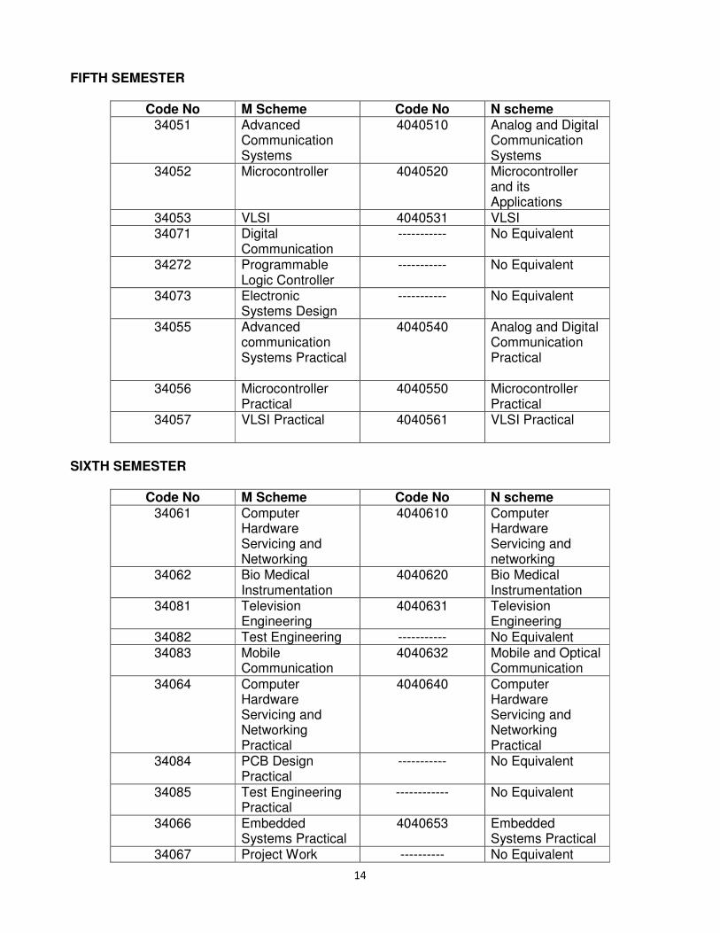
FIFTH SEMESTER
Code No M Scheme Code No N scheme 34051 Advanced
Communication Systems
4040510 Analog and Digital Communication Systems
34052 Microcontroller 4040520 Microcontroller and its Applications
34053 VLSI 4040531 VLSI 34071 Digital
Communication ----------- No Equivalent
34272 Programmable Logic Controller
-----------
No Equivalent
34073 Electronic Systems Design
-----------
No Equivalent
34055 Advanced communication Systems Practical
4040540 Analog and Digital Communication Practical
34056 Microcontroller Practical
4040550 Microcontroller Practical
34057 VLSI Practical 4040561 VLSI Practical
SIXTH SEMESTER
Code No M Scheme Code No N scheme 34061 Computer
Hardware Servicing and Networking
4040610 Computer Hardware Servicing and networking
34062 Bio Medical Instrumentation
4040620 Bio Medical Instrumentation
34081 Television Engineering
4040631 Television Engineering
34082 Test Engineering ----------- No Equivalent 34083 Mobile
Communication 4040632 Mobile and Optical
Communication
34064 Computer Hardware Servicing and Networking Practical
4040640 Computer Hardware Servicing and Networking Practical
34084 PCB Design Practical
----------- No Equivalent
34085 Test Engineering Practical
------------ No Equivalent
34066 Embedded Systems Practical
4040653 Embedded Systems Practical
34067 Project Work ---------- No Equivalent
15
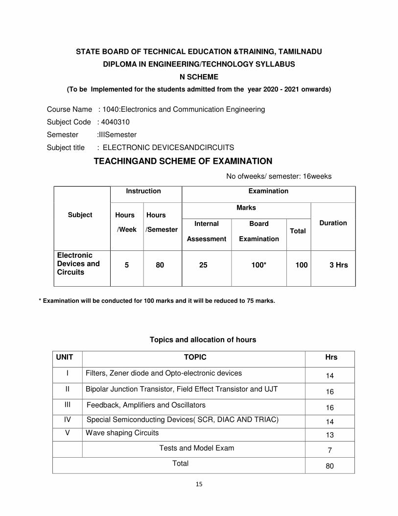
STATE BOARD OF TECHNICAL EDUCATION &TRAINING, TAMILNADU
DIPLOMA IN ENGINEERING/TECHNOLOGY SYLLABUS
N SCHEME
(To be Implemented for the students admitted from the year 2020 - 2021 onwards)
Course Name : 1040:Electronics and Communication Engineering
Subject Code : 4040310
Semester :IIISemester
Subject title : ELECTRONIC DEVICESANDCIRCUITS
TEACHINGAND SCHEME OF EXAMINATION
No ofweeks/ semester: 16weeks
Subject
Instruction Examination
Hours
/Week
Hours
/Semester
Marks
Duration Internal
Assessment
Board
Examination
Total
Electronic Devices and Circuits
5
80
25
100*
100
3 Hrs
* Examination will be conducted for 100 marks and it will be reduced to 75 marks.
Topics and allocation of hours
UNIT TOPIC Hrs
I Filters, Zener diode and Opto-electronic devices 14
II Bipolar Junction Transistor, Field Effect Transistor and UJT 16
III Feedback, Amplifiers and Oscillators 16
IV Special Semiconducting Devices( SCR, DIAC AND TRIAC) 14
V Wave shaping Circuits 13
Tests and Model Exam 7
Total 80
16
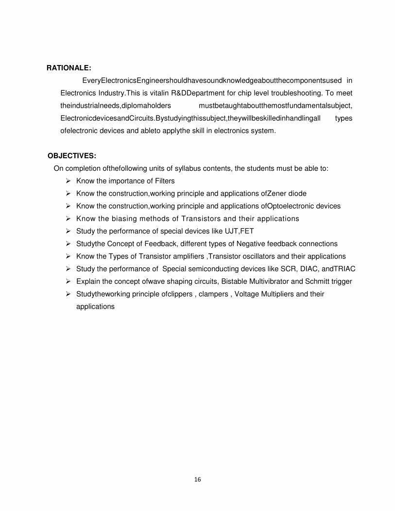
RATIONALE:
EveryElectronicsEngineershouldhavesoundknowledgeaboutthecomponentsused in
Electronics Industry.This is vitalin R&DDepartment for chip level troubleshooting. To meet
theindustrialneeds,diplomaholders mustbetaughtaboutthemostfundamentalsubject,
ElectronicdevicesandCircuits.Bystudyingthissubject,theywillbeskilledinhandlingall types
ofelectronic devices and ableto applythe skill in electronics system.
OBJECTIVES:
On completion ofthefollowing units of syllabus contents, the students must be able to:
� Know the importance of Filters
� Know the construction,working principle and applications ofZener diode
� Know the construction,working principle and applications ofOptoelectronic devices
� Know the biasing methods of Transistors and their applications
� Study the performance of special devices like UJT,FET
� Studythe Concept of Feedback, different types of Negative feedback connections
� Know the Types of Transistor amplifiers ,Transistor oscillators and their applications
� Study the performance of Special semiconducting devices like SCR, DIAC, andTRIAC
� Explain the concept ofwave shaping circuits, Bistable Multivibrator and Schmitt trigger
� Studytheworking principle ofclippers , clampers , Voltage Multipliers and their
applications
17
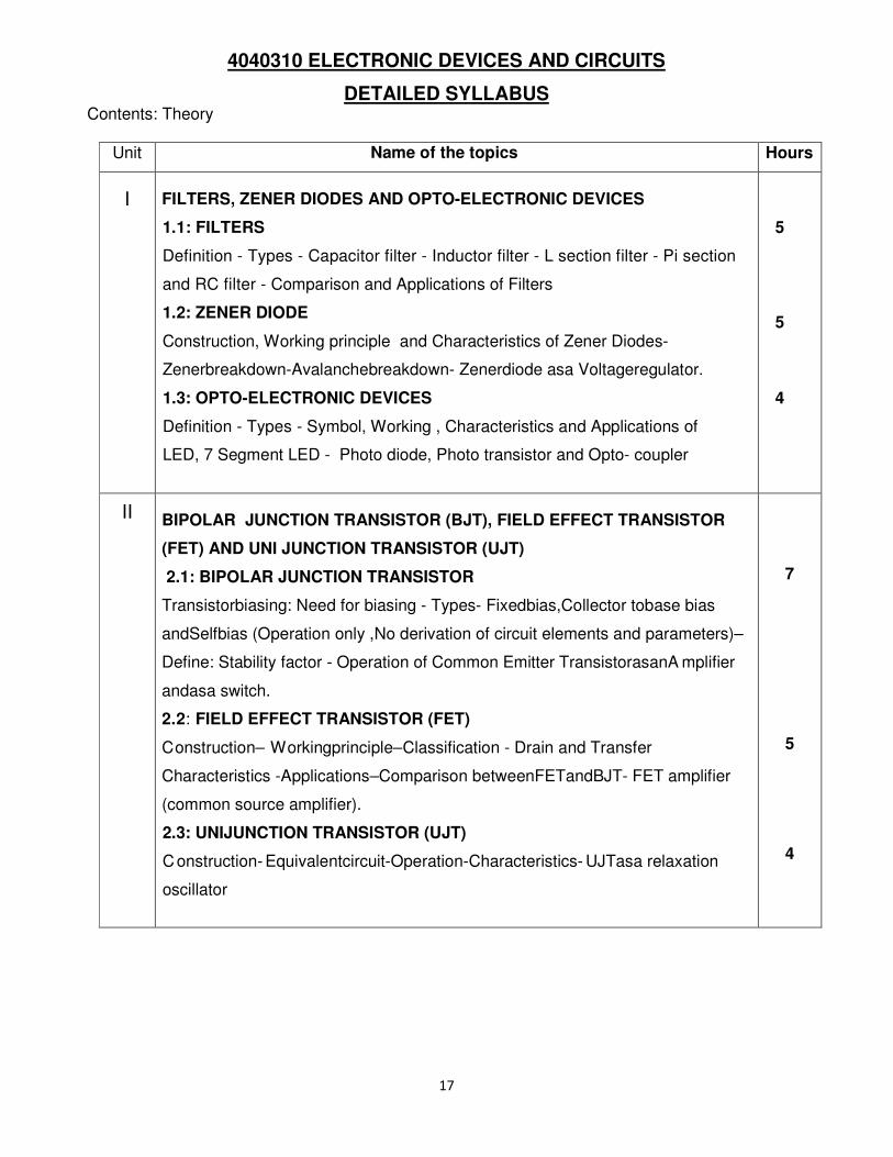
4040310 ELECTRONIC DEVICES AND CIRCUITS
DETAILED SYLLABUS Contents: Theory
Unit Name of the topics Hours
I
FILTERS, ZENER DIODES AND OPTO-ELECTRONIC DEVICES
1.1: FILTERS
Definition - Types - Capacitor filter - Inductor filter - L section filter - Pi section
and RC filter - Comparison and Applications of Filters
1.2: ZENER DIODE
Construction, Working principle and Characteristics of Zener Diodes-
Zenerbreakdown-Avalanchebreakdown- Zenerdiode asa Voltageregulator.
1.3: OPTO-ELECTRONIC DEVICES
Definition - Types - Symbol, Working , Characteristics and Applications of
LED, 7 Segment LED - Photo diode, Photo transistor and Opto- coupler
5 5 4
II
BIPOLAR JUNCTION TRANSISTOR (BJT), FIELD EFFECT TRANSISTOR
(FET) AND UNI JUNCTION TRANSISTOR (UJT)
2.1: BIPOLAR JUNCTION TRANSISTOR
Transistorbiasing: Need for biasing - Types- Fixedbias,Collector tobase bias
andSelfbias (Operation only ,No derivation of circuit elements and parameters)–
Define: Stability factor - Operation of Common Emitter TransistorasanA mplifier
andasa switch.
2.2: FIELD EFFECT TRANSISTOR (FET)
Construction– Workingprinciple–Classification - Drain and Transfer
Characteristics -Applications–Comparison betweenFETandBJT- FET amplifier
(common source amplifier).
2.3: UNIJUNCTION TRANSISTOR (UJT)
C onstruction- Equivalentcircuit-Operation-Characteristics- UJTasa relaxation
oscillator
7 5 4
18
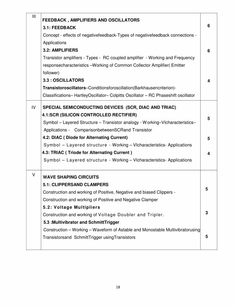
III FEEDBACK , AMPLIFIERS AND OSCILLATORS
3.1: FEEDBACK
Concept - effects of negativefeedback-Types of negativefeedback connections -
Applications
3.2: AMPLIFIERS
Transistor amplifiers - Types - RC coupled amplifier - Working and Frequency
responsecharacteristics –Working of Common Collector Amplifier( Emitter
follower)
3.3 : OSCILLATORS
Transistoroscillators–Conditionsforoscillation(Barkhausencriterion)-
Classifications– HartleyOscillator– Colpitts Oscillator – RC Phaseshift oscillator
6 6 4
IV
SPECIAL SEMICONDUCTING DEVICES (SCR, DIAC AND TRIAC)
4.1:SCR (SILICON CONTROLLED RECTIFIER)
Symbol – Layered Structure – Transistor analogy - W orking–VIcharacteristics–
Applications - ComparisonbetweenSCRand Transistor
4.2: DIAC ( Diode for Alternating Current)
Symbol – Layered structure - Working – VIcharacteristics- Applications
4.3: TRIAC ( Triode for Alternating Current )
Symbol – Layered structure - Working – VIcharacteristics- Applications
5 5 4
V WAVE SHAPING CIRCUITS
5.1: CLIPPERSAND CLAMPERS
Construction and working of Positive, Negative and biased Clippers -
Construction and working of Positive and Negative Clamper
5.2: Voltage Multipliers
Construction and working of Voltage Doubler and Tr ipler .
5.3 :Multivibrator and SchmittTrigger
Construction – Working – Waveform of Astable and Monostable Multivibratorusing
Transistorsand SchmittTrigger usingTransistors
5
3
5
19
Reference Books:
1. Electronics Devices & Circuits bySalivahananS,N.Suresh Kumar, A.Vallavaraj
Tata McGrawPublication 3rdEdition 2016
2. Electronics Devices and circuit theorybyBoyestad&Nashelsky, PHI , NewDelhi
2009
3. Electronic Principles byMalvino,-Tata McGrawHill Publication 2010.
4. ElectronicsDevices&CircuitsbyJacobMillmanandHalkias3rdEdition
2010, Tata McGraw– Hill publication
5.Optical Fiber Communication byGerdKeiser 5th
Edition, Tata McGraw– Hill .
20
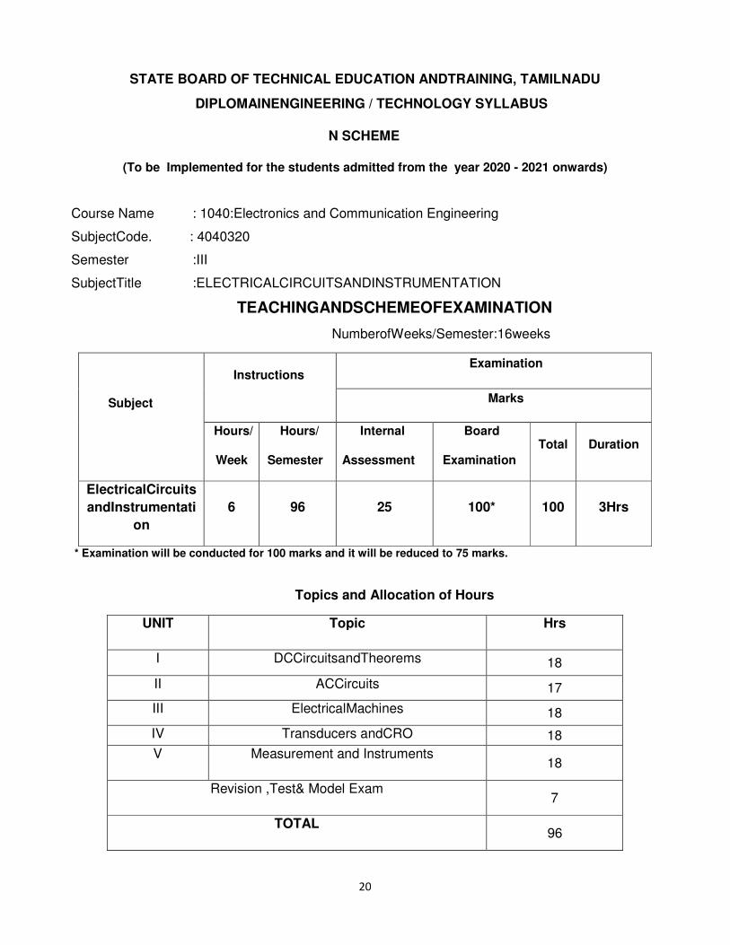
STATE BOARD OF TECHNICAL EDUCATION ANDTRAINING, TAMILNADU
DIPLOMAINENGINEERING / TECHNOLOGY SYLLABUS
N SCHEME
(To be Implemented for the students admitted from the year 2020 - 2021 onwards)
Course Name : 1040:Electronics and Communication Engineering
SubjectCode. : 4040320
Semester :III
SubjectTitle :ELECTRICALCIRCUITSANDINSTRUMENTATION
TEACHINGANDSCHEMEOFEXAMINATION
NumberofWeeks/Semester:16weeks
Subject
Instructions
Examination
Marks
Hours/
Week
Hours/
Semester
Internal
Assessment
Board
Examination
Total
Duration
ElectricalCircuits
andInstrumentati
on
6
96
25
100*
100
3Hrs
* Examination will be conducted for 100 marks and it will be reduced to 75 marks.
Topics and Allocation of Hours
UNIT Topic Hrs
I DCCircuitsandTheorems 18
II ACCircuits 17
III ElectricalMachines 18
IV Transducers andCRO 18
V Measurement and Instruments 18
Revision ,Test& Model Exam 7
TOTAL 96
21
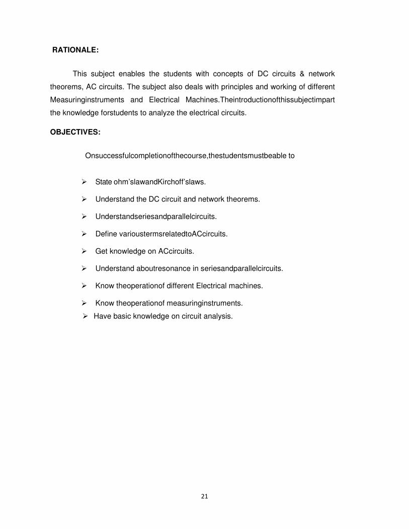
RATIONALE:
This subject enables the students with concepts of DC circuits & network
theorems, AC circuits. The subject also deals with principles and working of different
Measuringinstruments and Electrical Machines.Theintroductionofthissubjectimpart
the knowledge forstudents to analyze the electrical circuits.
OBJECTIVES:
Onsuccessfulcompletionofthecourse,thestudentsmustbeable to
� State ohm’slawandKirchoff’slaws.
� Understand the DC circuit and network theorems.
� Understandseriesandparallelcircuits.
� Define varioustermsrelatedtoACcircuits.
� Get knowledge on ACcircuits.
� Understand aboutresonance in seriesandparallelcircuits.
� Know theoperationof different Electrical machines.
� Know theoperationof measuringinstruments.
� Have basic knowledge on circuit analysis.
22
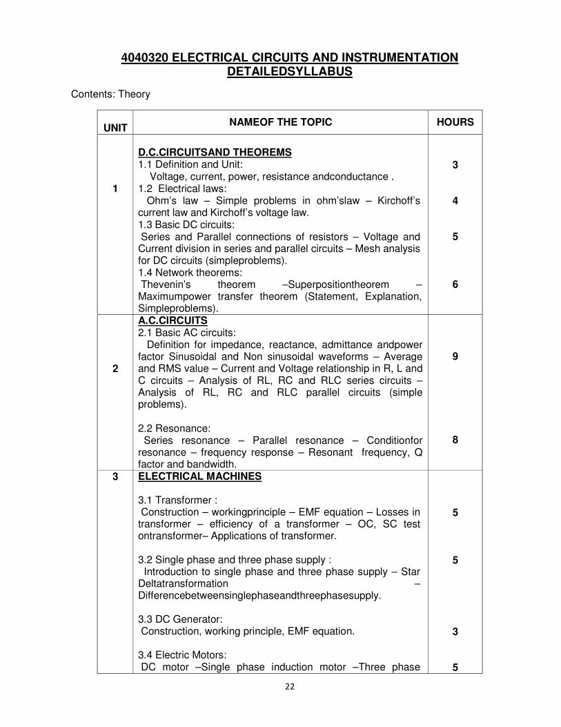
4040320 ELECTRICAL CIRCUITS AND INSTRUMENTATION DETAILEDSYLLABUS
Contents: Theory
UNIT
NAMEOF THE TOPIC HOURS
1
D.C.CIRCUITSAND THEOREMS 1.1 Definition and Unit: Voltage, current, power, resistance andconductance . 1.2 Electrical laws: Ohm’s law – Simple problems in ohm’slaw – Kirchoff’s current law and Kirchoff’s voltage law. 1.3 Basic DC circuits: Series and Parallel connections of resistors – Voltage and Current division in series and parallel circuits – Mesh analysis for DC circuits (simpleproblems). 1.4 Network theorems: Thevenin’s theorem –Superpositiontheorem –Maximumpower transfer theorem (Statement, Explanation, Simpleproblems).
3
4
5
6
2
A.C.CIRCUITS 2.1 Basic AC circuits: Definition for impedance, reactance, admittance andpower factor Sinusoidal and Non sinusoidal waveforms – Average and RMS value – Current and Voltage relationship in R, L and C circuits – Analysis of RL, RC and RLC series circuits – Analysis of RL, RC and RLC parallel circuits (simple problems). 2.2 Resonance: Series resonance – Parallel resonance – Conditionfor resonance – frequency response – Resonant frequency, Q factor and bandwidth.
9
8
3
ELECTRICAL MACHINES 3.1 Transformer : Construction – workingprinciple – EMF equation – Losses in transformer – efficiency of a transformer – OC, SC test ontransformer– Applications of transformer. 3.2 Single phase and three phase supply : Introduction to single phase and three phase supply – Star Deltatransformation – Differencebetweensinglephaseandthreephasesupply. 3.3 DC Generator: Construction, working principle, EMF equation. 3.4 Electric Motors: DC motor –Single phase induction motor –Three phase
5
5
3
5
23
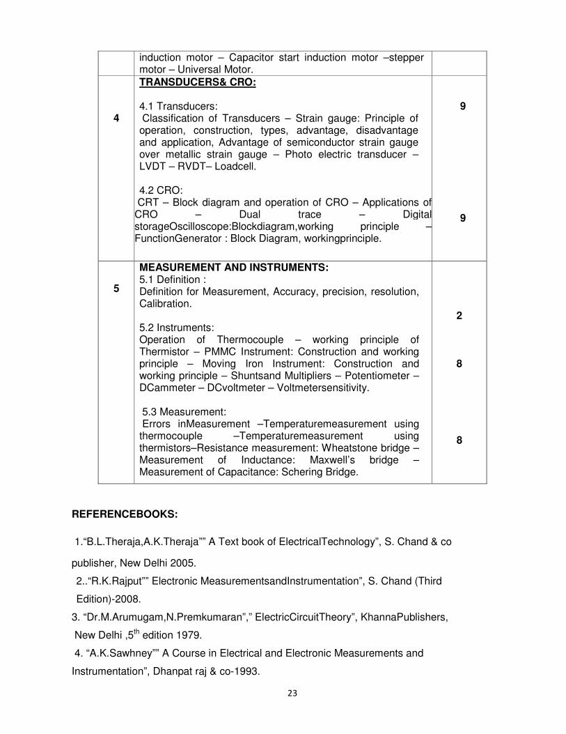
induction motor – Capacitor start induction motor –stepper motor – Universal Motor.
4
TRANSDUCERS& CRO: 4.1 Transducers: Classification of Transducers – Strain gauge: Principle of operation, construction, types, advantage, disadvantage and application, Advantage of semiconductor strain gauge over metallic strain gauge – Photo electric transducer – LVDT – RVDT– Loadcell. 4.2 CRO:
CRT – Block diagram and operation of CRO – Applications of CRO – Dual trace – Digital storageOscilloscope:Blockdiagram,working principle –FunctionGenerator : Block Diagram, workingprinciple.
9
9
5
MEASUREMENT AND INSTRUMENTS: 5.1 Definition : Definition for Measurement, Accuracy, precision, resolution, Calibration. 5.2 Instruments: Operation of Thermocouple – working principle of Thermistor – PMMC Instrument: Construction and working principle – Moving Iron Instrument: Construction and working principle – Shuntsand Multipliers – Potentiometer – DCammeter – DCvoltmeter – Voltmetersensitivity. 5.3 Measurement: Errors inMeasurement –Temperaturemeasurement using thermocouple –Temperaturemeasurement using thermistors–Resistance measurement: Wheatstone bridge – Measurement of Inductance: Maxwell’s bridge – Measurement of Capacitance: Schering Bridge.
2 8
8
REFERENCEBOOKS:
1.“B.L.Theraja,A.K.Theraja”” A Text book of ElectricalTechnology”, S. Chand & co
publisher, New Delhi 2005.
2..“R.K.Rajput”” Electronic MeasurementsandInstrumentation”, S. Chand (Third
Edition)-2008.
3. “Dr.M.Arumugam,N.Premkumaran”,” ElectricCircuitTheory”, KhannaPublishers,
New Delhi ,5th edition 1979.
4. “A.K.Sawhney”” A Course in Electrical and Electronic Measurements and
Instrumentation”, Dhanpat raj & co-1993.
24
STATE BOARD OF TECHNICAL EDUCATION &TRAINING, TAMILNADU
DIPLOMA IN ENGINEERING/TECHNOLOGY SYLLABUS
N SCHEME
(To be Implementedfor the students admitted from the year 2020 - 2021 onwards)
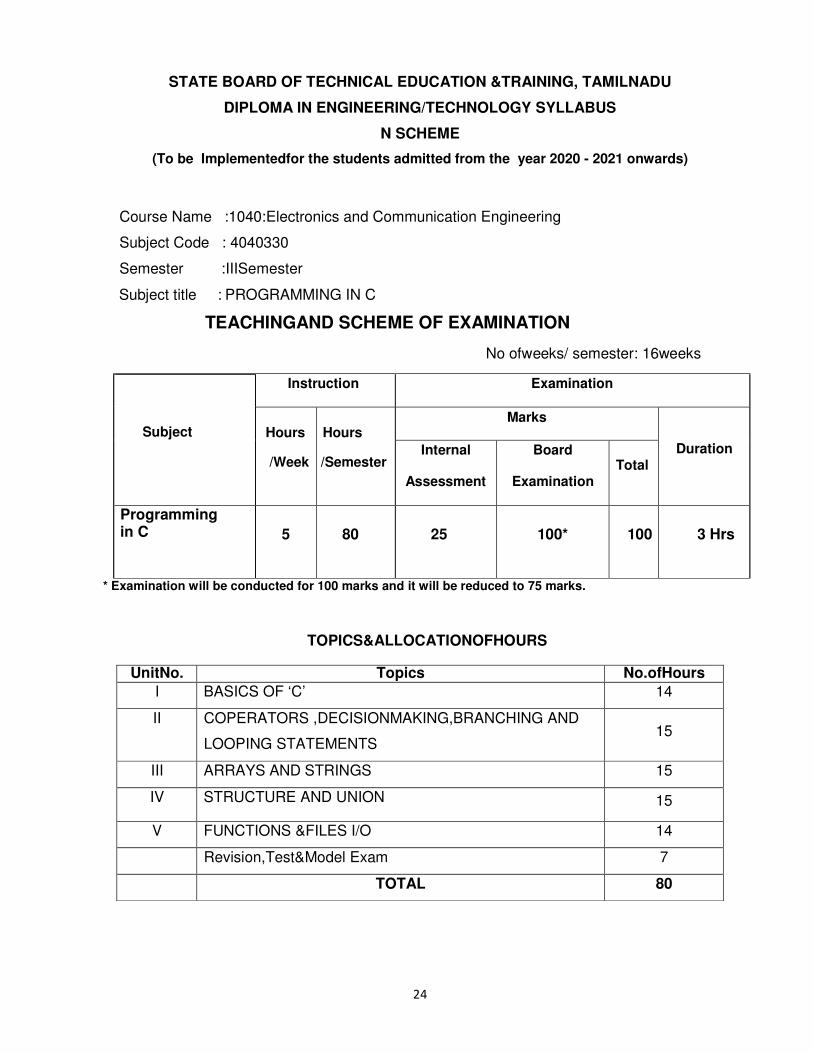
Course Name :1040:Electronics and Communication Engineering
Subject Code : 4040330
Semester :IIISemester
Subject title : PROGRAMMING IN C
TEACHINGAND SCHEME OF EXAMINATION
No ofweeks/ semester: 16weeks
Subject
Instruction Examination
Hours
/Week
Hours
/Semester
Marks Duration Internal
Assessment
Board
Examination
Total
Programming in C
5
80
25
100*
100
3 Hrs
* Examination will be conducted for 100 marks and it will be reduced to 75 marks.
TOPICS&ALLOCATIONOFHOURS
UnitNo. Topics No.ofHours
I BASICS OF ‘C’ 14
II COPERATORS ,DECISIONMAKING,BRANCHING AND
LOOPING STATEMENTS 15
III ARRAYS AND STRINGS 15
IV STRUCTURE AND UNION 15
V FUNCTIONS &FILES I/O 14
Revision,Test&Model Exam 7
TOTAL 80
25
RATIONALE:
‘C’ language is the most widely used computer language, which is being taught as
a core course. C is the generalpurpose high level language. Due to the flexibility, it is
suitable for different development environments. ‘C’ language has importance and
popularity in recently developed and advanced softwareindustry. ‘C’ language can also
be used for system level programming and it is still considered as first
priorityprogramming language. This course covers the basic concepts of ‘C’.
OBJECTIVES:
The course aims to provide exposure / train the students to do programming in C.
AttheendoftheCourse,thestudents will be able to
� Know the basics of C.
� Writealgorithm andflowchartforanyproblems.
� Know operators used in ‘C’ and Decision making statements.
� Define and understand aboutarraysandfunctions.
� Defineand understand aboutstructureandunion.
� Understand strings, string handling functions.
� Developprogramsusing C operators, decision making statements.
� Developprogramsusing arrays, function, and structure.
26
4040330PROGRAMMINGINC DETAILEDSYLLABUS
Contents: Theory
UNIT NAMEOF THE TOPICS HOURS
I BASICS OF C:
1.1 Introduction to C: History of ‘C’ – Structure of C program – Steps for execution of C program – Functions performed by Compiler, Linker – Algorithm & flow chart – Low level and High level Programming language – C character set –Tokens –Constants – Key words – Variables – Data types – Declaration of Variables – Assigningvaluestovariables .
1.2 I/O statements: Formatted input, Formatted output, Unformatted I/O statements.
8
6
II C OPERATORS , DECISIONMAKING,BRANCHING AND LOOPING STATEMENTS:
2.1 C operators: Arithmetic, Logical, Assignment, Relational,Increment,Decrement,Conditional,Bitwise and Special operators –Precedence and Associativity – C expressions: Arithmeticexpressions, Evaluation ofexpressions. 2.2 Decisionmaking,branching and looping statements:
Simpleifstatement ,if- else,else-if ladderand nestedif-else statement –switchstatement – while, do-while statements – for loop, go to, break& continuestatement – Programtofindwhetherthegivennumberiseven or odd – ProgramtoperformtheArithmeticoperationsusingswitchstatement – Program to find sum of series using “while” loop .
7
8
III ARRAYS AND STRINGS:
3.1 Arrays: Definition of array – Declaration andinitializationofOnedimensional,Two dimensional arrays –Accessing array elements –Program to find sum of the elements of array – Program for matrix addition.
3.2 STRINGS: Declaration and initialization of string variables, String handling Functions: strlen (), strcpy() , strcat(), strcmp() – Program to sort the set of strings using string handling functions.
8 7
27
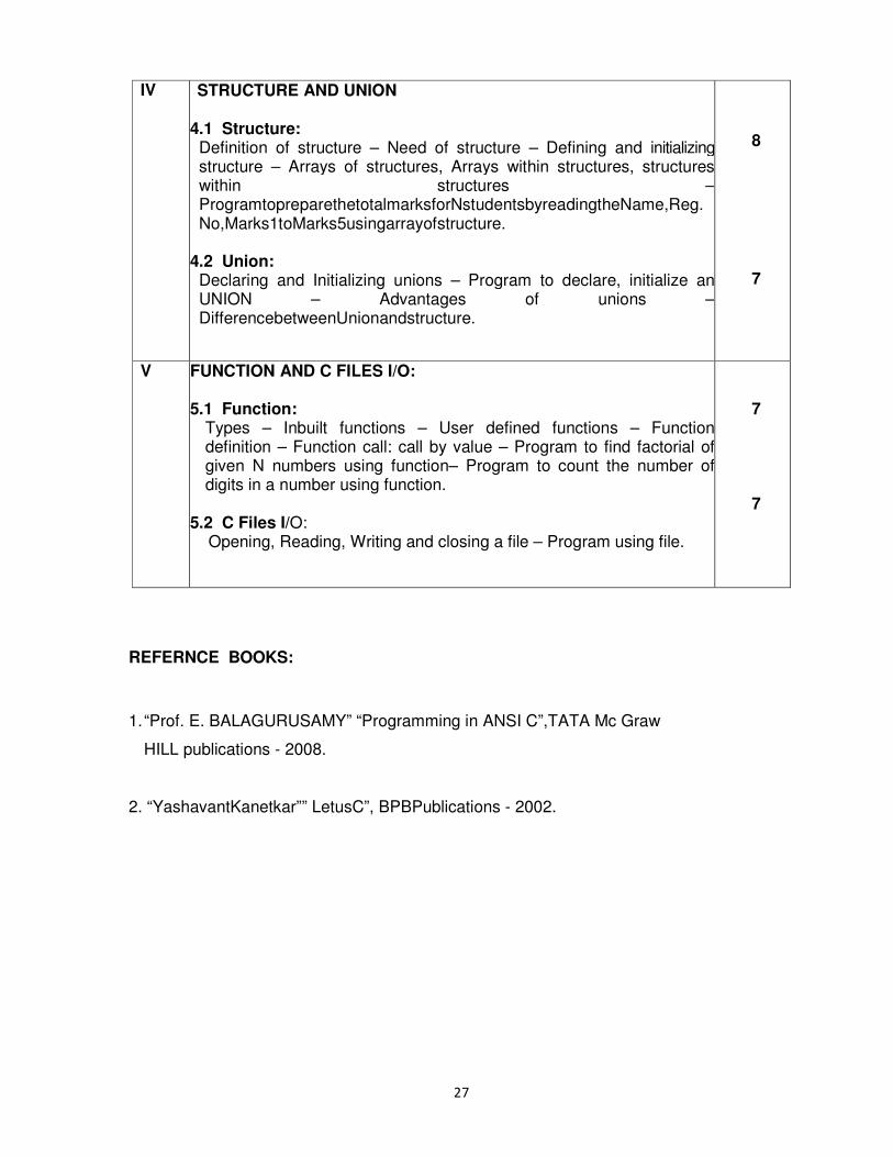
IV STRUCTURE AND UNION
4.1 Structure: Definition of structure – Need of structure – Defining and initializingstructure – Arrays of structures, Arrays within structures, structures within structures –ProgramtopreparethetotalmarksforNstudentsbyreadingtheName,Reg.No,Marks1toMarks5usingarrayofstructure.
4.2 Union: Declaring and Initializing unions – Program to declare, initialize an UNION – Advantages of unions –DifferencebetweenUnionandstructure.
8
7
V FUNCTION AND C FILES I/O:
5.1 Function:
Types – Inbuilt functions – User defined functions – Function definition – Function call: call by value – Program to find factorial of given N numbers using function– Program to count the number of digits in a number using function.
5.2 C Files I/O: Opening, Reading, Writing and closing a file – Program using file.
7 7
REFERNCE BOOKS:
1. “Prof. E. BALAGURUSAMY” “Programming in ANSI C”,TATA Mc Graw
HILL publications - 2008.
2. “YashavantKanetkar”” LetusC”, BPBPublications - 2002.
28
STATE BOARD OF TECHNICAL EDUCATION &TRAINING, TAMILNADU
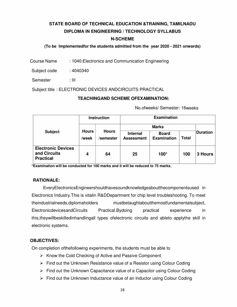
DIPLOMA IN ENGINEERING / TECHNOLOGY SYLLABUS
N-SCHEME
(To be Implementedfor the students admitted from the year 2020 - 2021 onwards)
Course Name : 1040:Electronics and Communication Engineering
Subject code : 4040340 Semester : III
Subject title : ELECTRONIC DEVICES ANDCIRCUITS PRACTICAL
TEACHINGAND SCHEME OFEXAMINATION:
No.ofweeks/ Semester: 16weeks
Subject
Instruction Examination
Hours
/week
Hours
/semester
Marks
Duration Internal Assessment
Board Examination
Total
Electronic Devices and Circuits Practical
4
64
25
100*
100
3 Hours
*Examination will be conducted for 100 marks and it will be reduced to 75 marks.
RATIONALE:
EveryElectronicsEngineershouldhavesoundknowledgeaboutthecomponentsused in
Electronics Industry.This is vitalin R&DDepartment for chip level troubleshooting. To meet
theindustrialneeds,diplomaholders mustbetaughtaboutthemostfundamentalsubject,
ElectronicdevicesandCircuits Practical.Bydoing practical experience in
this,theywillbeskilledinhandlingall types ofelectronic circuits and ableto applythe skill in
electronic systems.
OBJECTIVES:
On completion ofthefollowing experiments, the students must be able to
� Know the Cold Checking of Active and Passive Component
� Find out the Unknown Resistance value of a Resistor using Colour Coding
� Find out the Unknown Capacitance value of a Capacitor using Colour Coding
� Find out the Unknown Inductance value of an Inductor using Colour Coding
29
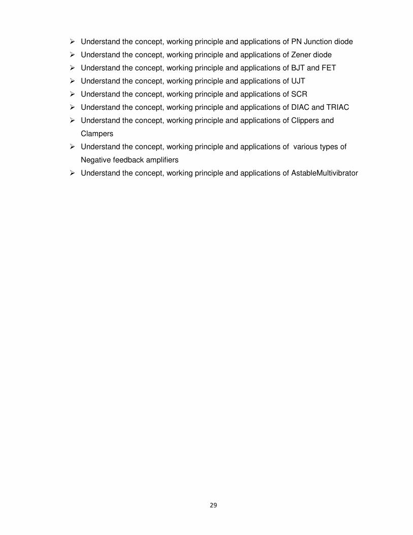
� Understand the concept, working principle and applications of PN Junction diode
� Understand the concept, working principle and applications of Zener diode
� Understand the concept, working principle and applications of BJT and FET
� Understand the concept, working principle and applications of UJT
� Understand the concept, working principle and applications of SCR
� Understand the concept, working principle and applications of DIAC and TRIAC
� Understand the concept, working principle and applications of Clippers and
Clampers
� Understand the concept, working principle and applications of various types of
Negative feedback amplifiers
� Understand the concept, working principle and applications of AstableMultivibrator
30
4040340 ELECTRONIC DEVICES AND CIRCUITS PRACTICAL
DETAILED SYLLABUS Contents: Practical
Exercises
Note: At least 5 experiments should be done using Soldering board / Bread board
1. Construct a circuit to test the forward and reverse bias characteristics of a PN Junction
Silicon diode. Find the value of its cut-in voltage
2. Construct a circuit to test the forward and reverse bias characteristics of a Zener diode.
Find the value of its reverse breakdown voltage
3. Construct a Full wave (center tapped) rectifier and test its input and output waveforms
with and without Capacitor filter. Find its maximum voltage.
4. Construct a Full wave (Bridge) rectifier and test its input and output waveforms with and
without Capacitor filter. Find its maximum voltage.
5. Construct a Common Emitter Transistor circuit and test its input and output characteristic
curves.
6. Construct a Common Source Field Effect Transistor circuit and test its drain and transfer
characteristic curves.
7. Construct a circuit to test the Turning on and Turning off characteristics of SCR and find
out the forward break over voltage, the value of Latching and Holding currents.
8. Construct a circuit to test the bidirectional characteristics of DIAC and plot its switching
characteristics.
9. Construct a circuit to test the bidirectional characteristics of TRIAC and plot its switching
characteristics.
10. Construct a Common emitter amplifier circuit and test its frequency response
characteristics with and without Current series feedback introduced in it.
11. Construct a circuit to test the switching characteristics of AstableMultivibrator
12. Construct a circuit totest the negative resistance Characteristics of UJT.
31
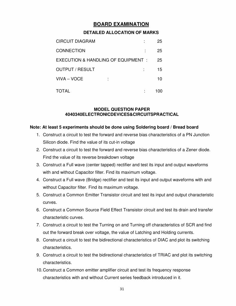
BOARD EXAMINATION
DETAILED ALLOCATION OF MARKS
CIRCUIT DIAGRAM : 25 CONNECTION :
25
EXECUTION & HANDLING OF EQUIPMENT :
25
OUTPUT / RESULT :
15
VIVA – VOCE :
10
TOTAL : 100
MODEL QUESTION PAPER
4040340ELECTRONICDEVICES&CIRCUITSPRACTICAL
Note: At least 5 experiments should be done using Soldering board / Bread board
1. Construct a circuit to test the forward and reverse bias characteristics of a PN Junction
Silicon diode. Find the value of its cut-in voltage
2. Construct a circuit to test the forward and reverse bias characteristics of a Zener diode.
Find the value of its reverse breakdown voltage
3. Construct a Full wave (center tapped) rectifier and test its input and output waveforms
with and without Capacitor filter. Find its maximum voltage.
4. Construct a Full wave (Bridge) rectifier and test its input and output waveforms with and
without Capacitor filter. Find its maximum voltage.
5. Construct a Common Emitter Transistor circuit and test its input and output characteristic
curves.
6. Construct a Common Source Field Effect Transistor circuit and test its drain and transfer
characteristic curves.
7. Construct a circuit to test the Turning on and Turning off characteristics of SCR and find
out the forward break over voltage, the value of Latching and Holding currents.
8. Construct a circuit to test the bidirectional characteristics of DIAC and plot its switching
characteristics.
9. Construct a circuit to test the bidirectional characteristics of TRIAC and plot its switching
characteristics.
10. Construct a Common emitter amplifier circuit and test its frequency response
characteristics with and without Current series feedback introduced in it.
32
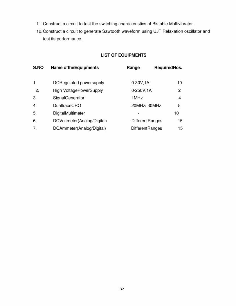
11. Construct a circuit to test the switching characteristics of Bistable Multivibrator .
12. Construct a circuit to generate Sawtooth waveform using UJT Relaxation oscillator and
test its performance.
LIST OF EQUIPMENTS
S.NO Name oftheEquipments Range RequiredNos.
1. DCRegulated powersupply 0-30V,1A 10
2. High VoltagePowerSupply 0-250V,1A 2
3. SignalGenerator 1MHz 4
4. DualtraceCRO 20MHz/ 30MHz 5
5. DigitalMultimeter - 10
6. DCVoltmeter(Analog/Digital) DifferentRanges 15
7. DCAmmeter(Analog/Digital) DifferentRanges 15
33
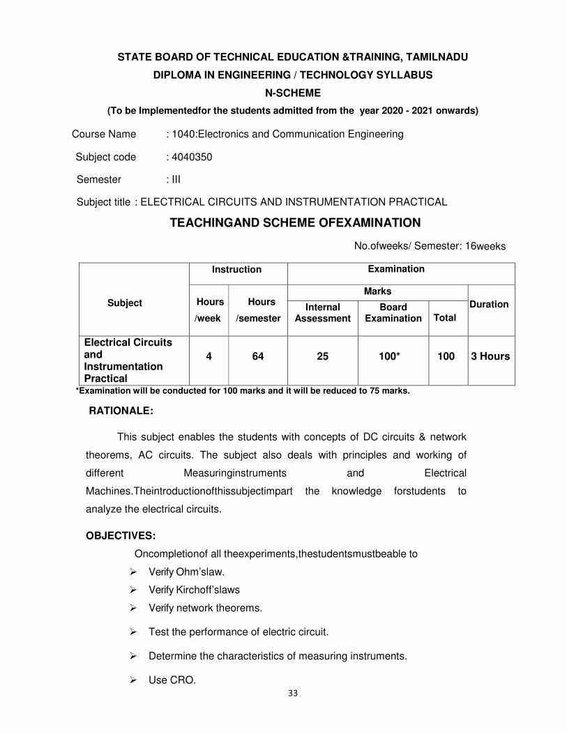
STATE BOARD OF TECHNICAL EDUCATION &TRAINING, TAMILNADU
DIPLOMA IN ENGINEERING / TECHNOLOGY SYLLABUS
N-SCHEME
(To be Implementedfor the students admitted from the year 2020 - 2021 onwards)
Course Name : 1040:Electronics and Communication Engineering
Subject code : 4040350 Semester : III
Subject title : ELECTRICAL CIRCUITS AND INSTRUMENTATION PRACTICAL
TEACHINGAND SCHEME OFEXAMINATION
No.ofweeks/ Semester: 16weeks
Subject
Instruction Examination
Hours
/week
Hours
/semester
Marks
Duration Internal Assessment
Board Examination
Total
Electrical Circuits and Instrumentation Practical
4
64
25
100*
100
3 Hours
*Examination will be conducted for 100 marks and it will be reduced to 75 marks.
RATIONALE:
This subject enables the students with concepts of DC circuits & network
theorems, AC circuits. The subject also deals with principles and working of
different Measuringinstruments and Electrical
Machines.Theintroductionofthissubjectimpart the knowledge forstudents to
analyze the electrical circuits.
OBJECTIVES:
Oncompletionof all theexperiments,thestudentsmustbeable to
� Verify Ohm’slaw.
� Verify Kirchoff’slaws
� Verify network theorems.
� Test the performance of electric circuit.
� Determine the characteristics of measuring instruments.
� Use CRO.
34
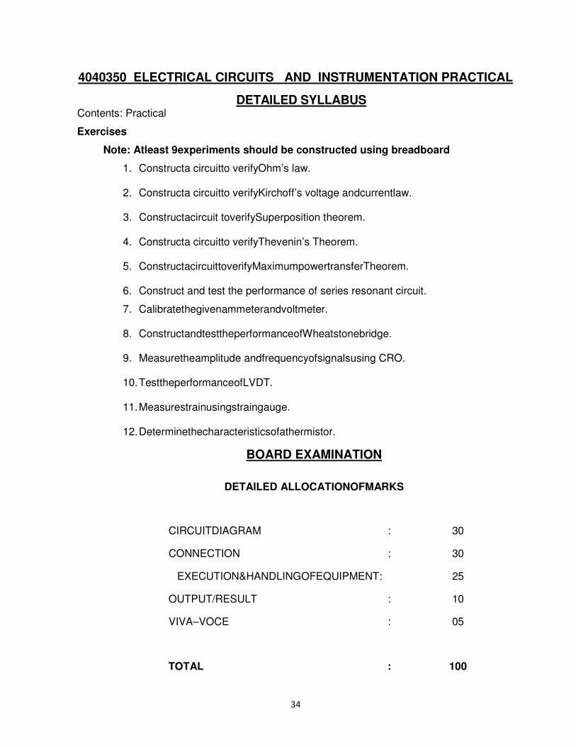
4040350 ELECTRICAL CIRCUITS AND INSTRUMENTATION PRACTICAL
DETAILED SYLLABUS Contents: Practical
Exercises
Note: Atleast 9experiments should be constructed using breadboard
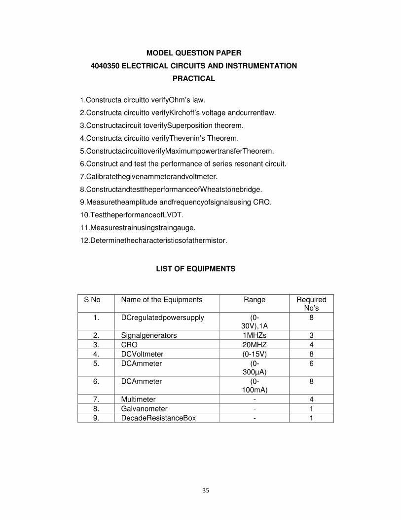
1. Constructa circuitto verifyOhm’s law.
2. Constructa circuitto verifyKirchoff’s voltage andcurrentlaw.
3. Constructacircuit toverifySuperposition theorem.
4. Constructa circuitto verifyThevenin’s Theorem.
5. ConstructacircuittoverifyMaximumpowertransferTheorem.
6. Construct and test the performance of series resonant circuit.
7. Calibratethegivenammeterandvoltmeter.
8. ConstructandtesttheperformanceofWheatstonebridge.
9. Measuretheamplitude andfrequencyofsignalsusing CRO.
10. TesttheperformanceofLVDT.
11. Measurestrainusingstraingauge.
12. Determinethecharacteristicsofathermistor.
BOARD EXAMINATION
DETAILED ALLOCATIONOFMARKS
CIRCUITDIAGRAM : 30
CONNECTION : 30
EXECUTION&HANDLINGOFEQUIPMENT: 25
OUTPUT/RESULT : 10
VIVA–VOCE : 05
TOTAL :
100
35
MODEL QUESTION PAPER
4040350 ELECTRICAL CIRCUITS AND INSTRUMENTATION
PRACTICAL
1.Constructa circuitto verifyOhm’s law.
2.Constructa circuitto verifyKirchoff’s voltage andcurrentlaw.
3.Constructacircuit toverifySuperposition theorem.
4.Constructa circuitto verifyThevenin’s Theorem.
5.ConstructacircuittoverifyMaximumpowertransferTheorem.
6.Construct and test the performance of series resonant circuit.
7.Calibratethegivenammeterandvoltmeter.
8.ConstructandtesttheperformanceofWheatstonebridge.
9.Measuretheamplitude andfrequencyofsignalsusing CRO.
10.TesttheperformanceofLVDT.
11.Measurestrainusingstraingauge.
12.Determinethecharacteristicsofathermistor.
LIST OF EQUIPMENTS
S No Name of the Equipments Range Required No’s
1. DCregulatedpowersupply (0-30V),1A
8
2. Signalgenerators 1MHZs 3
3. CRO 20MHZ 4
4. DCVoltmeter (0-15V) 8
5. DCAmmeter (0-300µA)
6
6. DCAmmeter (0-100mA)
8
7. Multimeter - 4
8. Galvanometer - 1
9. DecadeResistanceBox - 1
36
STATE BOARD OF TECHNICAL EDUCATION &TRAINING, TAMILNADU
DIPLOMA IN ENGINEERING / TECHNOLOGY SYLLABUS
N-SCHEME
(To be Implementedfor the students admitted from the year 2020 - 2021 onwards)
Course Name : 1040:Electronics and Communication Engineering
Subject code : 4040360
Semester : III
Subject title : PROGRAMMING IN C PRACTICAL
TEACHINGAND SCHEME OFEXAMINATION
No.ofweeks/ Semester: 16weeks
Subject
Instruction Examination
Hours
/week
Hours
/semester
Marks Duration
Internal Assessment
Board Examination
Total
Programming in C Practical
4
64
25
100*
100
3 Hours
*Examination will be conducted for 100 marks and it will be reduced to 75 marks.
RATIONALE: To Provide the platform for software
OBJECTIVES:
At the end of the Course, the students will be able to
• Thinkthelogictosolvethegivenproblem.
• Know the concepts of constants, variables, data types and
operators
• Developprograms to evaluate expression by knowing ‘c’
precedence rule.
• Write programs using different decision making, looping
statements.
• Writeprogramsusingarrays, function and structure.
37
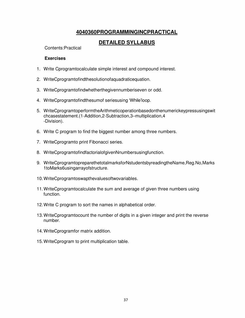
4040360PROGRAMMINGINCPRACTICAL
DETAILED SYLLABUS Contents:Practical Exercises
1. Write Cprogramtocalculate simple interest and compound interest.
2. WriteCprogramtofindthesolutionofaquadraticequation.
3. WriteCprogramtofindwhetherthegivennumberiseven or odd.
4. WriteCprogramtofindthesumof seriesusing ‘While’loop.
5. WriteCprogramtoperformtheArithmeticoperationbasedonthenumerickeypressusingswitchcasestatement.(1-Addition,2-Subtraction,3–multiplication,4 -Division).
6. Write C program to find the biggest number among three numbers.
7. WriteCprogramto print Fibonacci series.
8. WriteCprogramtofindfactorialofgivenNnumbersusingfunction.
9. WriteCprogramtopreparethetotalmarksforNstudentsbyreadingtheName,Reg.No,Marks1toMarks6usingarrayofstructure.
10. WriteCprogramtoswapthevaluesoftwovariables.
11. WriteCprogramtocalculate the sum and average of given three numbers using
function.
12. Write C program to sort the names in alphabetical order.
13. WriteCprogramtocount the number of digits in a given integer and print the reverse
number.
14. WriteCprogramfor matrix addition.
15. WriteCprogram to print multiplication table.
38
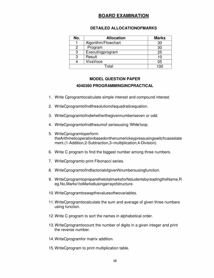
BOARD EXAMINATION
DETAILED ALLOCATIONOFMARKS
No. Allocation Marks
1 Algorithm/Flowchart 30 2 Program 30 3 Executingprogram 25 3 Result 10 4 VivaVoce 05
Total 100
MODEL QUESTION PAPER
4040360 PROGRAMMINGINCPRACTICAL
1. Write Cprogramtocalculate simple interest and compound interest.
2. WriteCprogramtofindthesolutionofaquadraticequation.
3. WriteCprogramtofindwhetherthegivennumberiseven or odd.
4. WriteCprogramtofindthesumof seriesusing ‘While’loop.
5. WriteCprogramtoperform theArithmeticoperationbasedonthenumerickeypressusingswitchcasestatement.(1-Addition,2-Subtraction,3–multiplication,4-Division).
6. Write C program to find the biggest number among three numbers.
7. WriteCprogramto print Fibonacci series.
8. WriteCprogramtofindfactorialofgivenNnumbersusingfunction.
9. WriteCprogramtopreparethetotalmarksforNstudentsbyreadingtheName,Reg.No,Marks1toMarks6usingarrayofstructure.
10. WriteCprogramtoswapthevaluesoftwovariables.
11. WriteCprogramtocalculate the sum and average of given three numbers
using function.
12. Write C program to sort the names in alphabetical order.
13. WriteCprogramtocount the number of digits in a given integer and print
the reverse number.
14. WriteCprogramfor matrix addition.
15. WriteCprogram to print multiplication table.
39
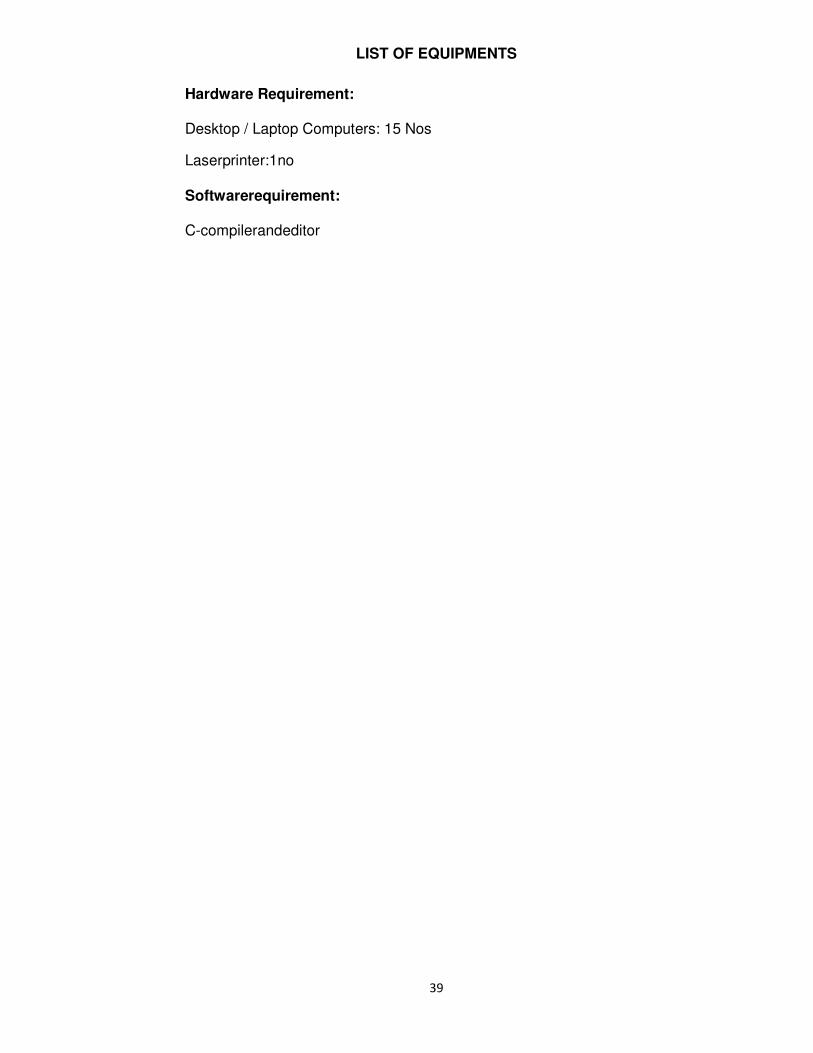
LIST OF EQUIPMENTS
Hardware Requirement:
Desktop / Laptop Computers: 15 Nos
Laserprinter:1no
Softwarerequirement:
C-compilerandeditor
40
STATE BOARD OF TECHNICAL EDUCATION &TRAINING, TAMILNADU
DIPLOMA IN ENGINEERING / TECHNOLOGY SYLLABUS
N-SCHEME
(To be Implementedfor the students admitted from the year 2020 - 2021 onwards)
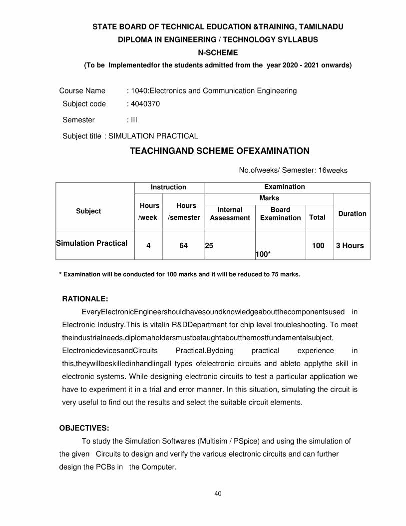
Course Name : 1040:Electronics and Communication Engineering
Subject code : 4040370 Semester : III
Subject title : SIMULATION PRACTICAL
TEACHINGAND SCHEME OFEXAMINATION
No.ofweeks/ Semester: 16weeks
Subject
Instruction Examination
Hours
/week
Hours
/semester
Marks
Duration Internal
Assessment Board
Examination
Total
Simulation Practical
4
64
25
100*
100
3 Hours
* Examination will be conducted for 100 marks and it will be reduced to 75 marks.
RATIONALE:
EveryElectronicEngineershouldhavesoundknowledgeaboutthecomponentsused in
Electronic Industry.This is vitalin R&DDepartment for chip level troubleshooting. To meet
theindustrialneeds,diplomaholdersmustbetaughtaboutthemostfundamentalsubject,
ElectronicdevicesandCircuits Practical.Bydoing practical experience in
this,theywillbeskilledinhandlingall types ofelectronic circuits and ableto applythe skill in
electronic systems. While designing electronic circuits to test a particular application we
have to experiment it in a trial and error manner. In this situation, simulating the circuit is
very useful to find out the results and select the suitable circuit elements.
OBJECTIVES:
To study the Simulation Softwares (Multisim / PSpice) and using the simulation of
the given Circuits to design and verify the various electronic circuits and can further
design the PCBs in the Computer.
41
4040370 SIMULATION PRACTICAL
DETAILED SYLLABUS Contents: Practical
Exercises
Note:
All experiments should be designed and verified through simulation tools like
Multisim/PSpice/Lab View/TINA
1. Zener diode (Forward and Reverse bias characteristics)
2. Rectifier circuits (Half wave and Full wave Bridge Rectifiers with Capacitor filter)
3. Power supply with Zener diode as Regulator
4. Common Base transistor output characteristics
5. Common emitter amplifier (Implementation of Current Series negative feedback)
6. Emitter follower (Implementation of Voltage Series negative feedback)
7. RC Coupled amplifier (Implementation of the concept of multistage amplifier)
8. Clippers and Clampers
9. RC Phase shift oscillator (Medium frequency Sine wave generators)
10. Hartley oscillator (High frequency Sine wave generator)
11. Astable Multivibrator (Square or Rectangular wave generator)
12. Gate triggering of SCR with various gate currents.
BOARD EXAMINATION
DETAILED ALLOCATION OF MARKS
CONNECTION ::
35
EXECUTION & HANDLING OF EQUIPMENT :
40
OUTPUT / RESULT :
15
VIVA – VOCE :
10
TOTAL : 100
MODEL QUESTION PAPER
4040370SIMULATIONPRACTICAL
Note:
All experiments should be designed and verified through simulation tools like
Multisim/PSpice/Lab View/TINA
42
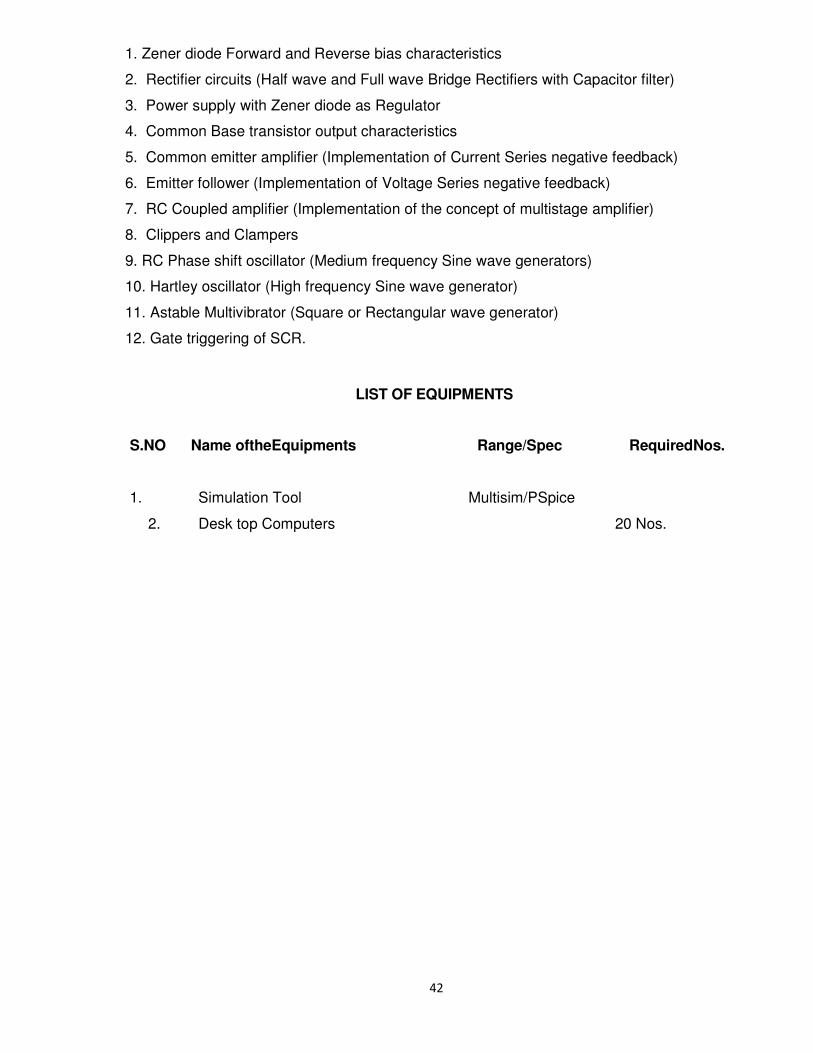
1. Zener diode Forward and Reverse bias characteristics
2. Rectifier circuits (Half wave and Full wave Bridge Rectifiers with Capacitor filter)
3. Power supply with Zener diode as Regulator
4. Common Base transistor output characteristics
5. Common emitter amplifier (Implementation of Current Series negative feedback)
6. Emitter follower (Implementation of Voltage Series negative feedback)
7. RC Coupled amplifier (Implementation of the concept of multistage amplifier)
8. Clippers and Clampers
9. RC Phase shift oscillator (Medium frequency Sine wave generators)
10. Hartley oscillator (High frequency Sine wave generator)
11. Astable Multivibrator (Square or Rectangular wave generator)
12. Gate triggering of SCR.
LIST OF EQUIPMENTS
S.NO Name oftheEquipments Range/Spec RequiredNos.
1. Simulation Tool Multisim/PSpice
2. Desk top Computers 20 Nos.
43
STATE BOARD OF TECHNICAL EDUCATION &TRAINING, TAMILNADU
DIPLOMA IN ENGINEERING / TECHNOLOGY SYLLABUS
N-SCHEME
(To be Implementedfor the students admitted from the year 2020 - 2021 onwards)
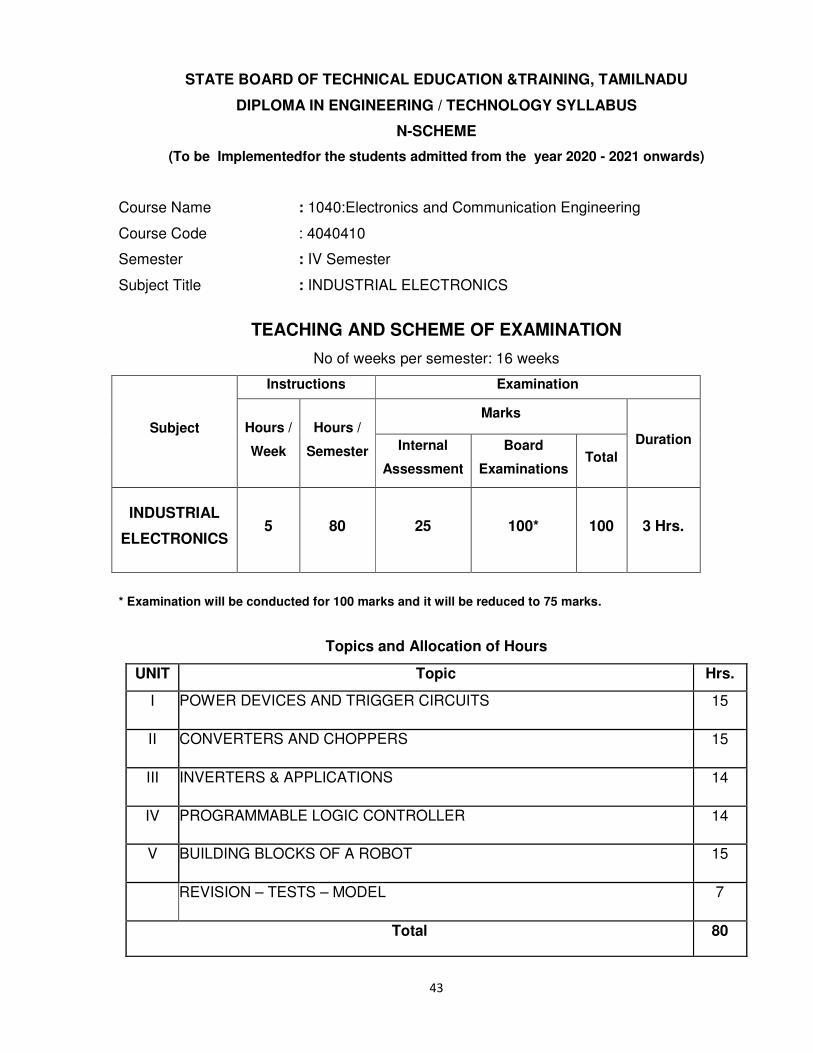
Course Name : 1040:Electronics and Communication Engineering
Course Code : 4040410
Semester : IV Semester
Subject Title : INDUSTRIAL ELECTRONICS
TEACHING AND SCHEME OF EXAMINATION
No of weeks per semester: 16 weeks
Subject
Instructions Examination
Hours /
Week
Hours /
Semester
Marks
Duration Internal
Assessment
Board
Examinations Total
INDUSTRIAL
ELECTRONICS 5 80 25 100* 100 3 Hrs.
* Examination will be conducted for 100 marks and it will be reduced to 75 marks.
Topics and Allocation of Hours
UNIT Topic Hrs.
I POWER DEVICES AND TRIGGER CIRCUITS 15
II CONVERTERS AND CHOPPERS 15
III INVERTERS & APPLICATIONS
14
IV PROGRAMMABLE LOGIC CONTROLLER 14
V BUILDING BLOCKS OF A ROBOT 15
REVISION – TESTS – MODEL 7
Total 80
44
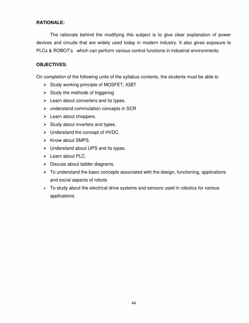
RATIONALE:
The rationale behind the modifying this subject is to give clear explanation of power
devices and circuits that are widely used today in modern industry. It also gives exposure to
PLCs & ROBOT’s which can perform various control functions in industrial environments.
OBJECTIVES:
On completion of the following units of the syllabus contents, the students must be able to
� Study working principle of MOSFET, IGBT
� Study the methods of triggering
� Learn about converters and its types.
� understand commutation concepts in SCR
� Learn about choppers.
� Study about inverters and types.
� Understand the concept of HVDC.
� Know about SMPS.
� Understand about UPS and its types.
� Learn about PLC.
� Discuss about ladder diagrams.
� To understand the basic concepts associated with the design, functioning, applications
and social aspects of robots
� To study about the electrical drive systems and sensors used in robotics for various
applications
45
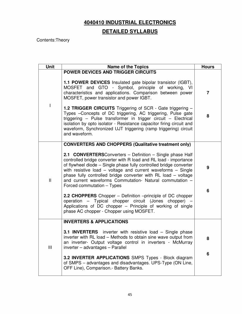
4040410 INDUSTRIAL ELECTRONICS
DETAILED SYLLABUS
Contents:Theory
Unit Name of the Topics Hours
I
POWER DEVICES AND TRIGGER CIRCUITS 1.1 POWER DEVICES Insulated gate bipolar transistor (IGBT), MOSFET and GTO - Symbol, principle of working, VI characteristics and applications. Comparison between power MOSFET, power transistor and power IGBT. 1.2 TRIGGER CIRCUITS Triggering of SCR - Gate triggering –Types –Concepts of DC triggering, AC triggering, Pulse gate triggering – Pulse transformer in trigger circuit – Electrical isolation by opto isolator - Resistance capacitor firing circuit and waveform, Synchronized UJT triggering (ramp triggering) circuit and waveform.
7
8
II
CONVERTERS AND CHOPPERS (Qualitative treatment only) 2.1 CONVERTERSConverters – Definition – Single phase Half controlled bridge converter with R load and RL load - importance of flywheel diode – Single phase fully controlled bridge converter with resistive load – voltage and current waveforms – Single phase fully controlled bridge converter with RL load – voltage and current waveforms Commutation- Natural commutation – Forced commutation – Types 2.2 CHOPPERS Chopper – Definition –principle of DC chopper operation – Typical chopper circuit (Jones chopper) –Applications of DC chopper – Principle of working of single phase AC chopper - Chopper using MOSFET.
9
6
III
INVERTERS & APPLICATIONS 3.1 INVERTERS inverter with resistive load – Single phase inverter with RL load – Methods to obtain sine wave output from an inverter- Output voltage control in inverters - McMurray inverter – advantages – Parallel 3.2 INVERTER APPLICATIONS SMPS Types - Block diagram of SMPS – advantages and disadvantages. UPS-Type (ON Line, OFF Line), Comparison.- Battery Banks.
8
6
46
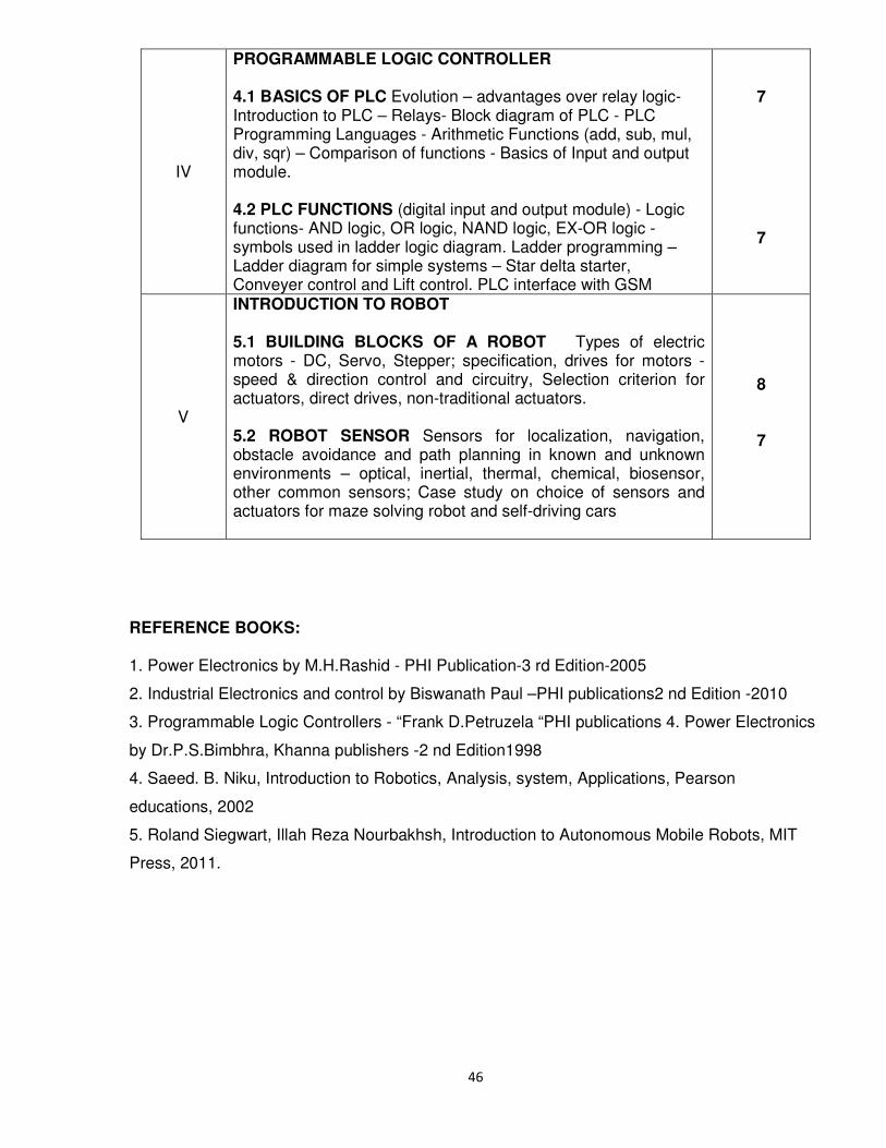
REFERENCE BOOKS: 1. Power Electronics by M.H.Rashid - PHI Publication-3 rd Edition-2005
2. Industrial Electronics and control by Biswanath Paul –PHI publications2 nd Edition -2010
3. Programmable Logic Controllers - “Frank D.Petruzela “PHI publications 4. Power Electronics
by Dr.P.S.Bimbhra, Khanna publishers -2 nd Edition1998
4. Saeed. B. Niku, Introduction to Robotics, Analysis, system, Applications, Pearson
educations, 2002
5. Roland Siegwart, Illah Reza Nourbakhsh, Introduction to Autonomous Mobile Robots, MIT
Press, 2011.
IV
PROGRAMMABLE LOGIC CONTROLLER 4.1 BASICS OF PLC Evolution – advantages over relay logic-Introduction to PLC – Relays- Block diagram of PLC - PLC Programming Languages - Arithmetic Functions (add, sub, mul, div, sqr) – Comparison of functions - Basics of Input and output module. 4.2 PLC FUNCTIONS (digital input and output module) - Logic functions- AND logic, OR logic, NAND logic, EX-OR logic -symbols used in ladder logic diagram. Ladder programming – Ladder diagram for simple systems – Star delta starter, Conveyer control and Lift control. PLC interface with GSM
7
7
V
INTRODUCTION TO ROBOT 5.1 BUILDING BLOCKS OF A ROBOT Types of electric motors - DC, Servo, Stepper; specification, drives for motors - speed & direction control and circuitry, Selection criterion for actuators, direct drives, non-traditional actuators. 5.2 ROBOT SENSOR Sensors for localization, navigation, obstacle avoidance and path planning in known and unknown environments – optical, inertial, thermal, chemical, biosensor, other common sensors; Case study on choice of sensors and actuators for maze solving robot and self-driving cars
8
7
47
STATE BOARD OF TECHNICAL EDUCATION &TRAINING, TAMILNADU
DIPLOMA IN ENGINEERING/TECHNOLOGY SYLLABUS
N SCHEME
(To be Implementedfor the students admitted from the year 2020 - 2021 onwards)
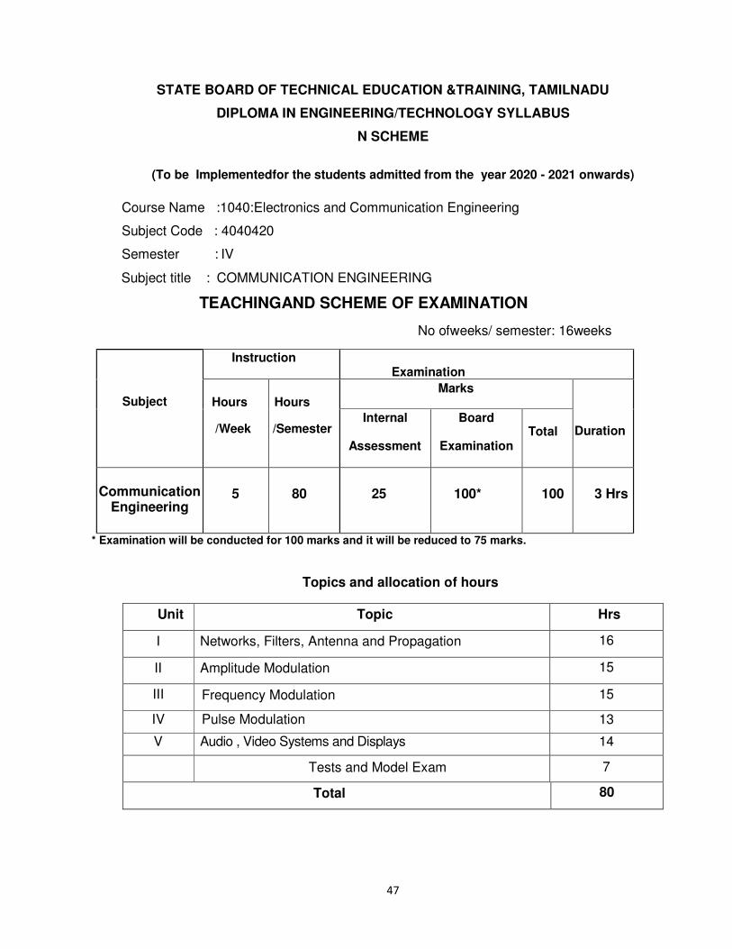
Course Name :1040:Electronics and Communication Engineering
Subject Code : 4040420
Semester : IV
Subject title : COMMUNICATION ENGINEERING
TEACHINGAND SCHEME OF EXAMINATION
No ofweeks/ semester: 16weeks
Subject
Instruction Examination
Hours
/Week
Hours
/Semester
Marks Duration
Internal
Assessment
Board
Examination
Total
Communication
Engineering
5
80
25
100*
100
3 Hrs
* Examination will be conducted for 100 marks and it will be reduced to 75 marks.
Topics and allocation of hours
Unit
Topic Hrs
I Networks, Filters, Antenna and Propagation 16
II Amplitude Modulation 15
III Frequency Modulation 15
IV Pulse Modulation 13
V Audio , Video Systems and Displays 14
Tests and Model Exam 7
Total 80
48
RATIONALE:
Todaycommunication engineering has developedto a great extent that there
isalways the need for studyofvarious communication concepts.Thissubject fulfills
the need forstudents to have a thorough knowledge of Filters,varioustypes of
Antennas, modulations, audio systems, video systems and displays
OBJECTIVES:
On completionofthefollowing units ofthe syllabus contents, the students must
be able to
� Understand the concepts of networks
� Understand the applications of Filters
� Know the Electro Magnetic Frequency Spectrum
� Know the relationship between Wave length and Frequency
� Understand the principlesofworking ofantennas
� Understand the theoryofPropagation
� Understand the conceptof modulation
� StudyAmplitude Modulation Process
� Learn about different types ofAM Transmitters&receivers
� Studythe FrequencyModulation Process
� Learn about different types ofFM Transmitters &Receivers
� Understand the conceptPulse Modulation
� Learn about different type of Pulse Analog modulation Techniques
� Learn about different type of Pulse Digital modulation Techniques
� Learn Different typesofMicrophones
� Learn Different typesofLoudspeaker
� Understand the principlesofMonochrome &colourTV fundamentals
� Understand the concept of Colour transmission and reception in PAL
COLOUR TV Receiver
� Understand the concept of various types of displays
49
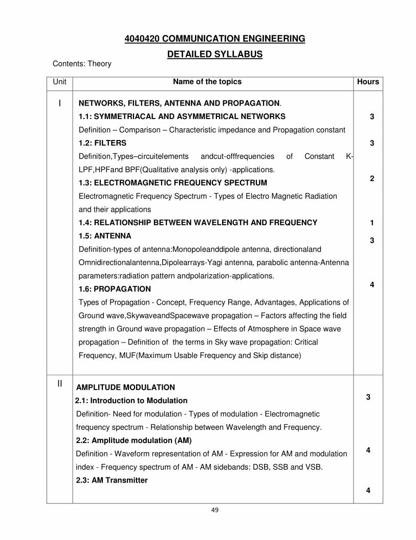
4040420 COMMUNICATION ENGINEERING
DETAILED SYLLABUS Contents: Theory Unit Name of the topics Hours
I
NETWORKS, FILTERS, ANTENNA AND PROPAGATION.
1.1: SYMMETRIACAL AND ASYMMETRICAL NETWORKS
Definition – Comparison – Characteristic impedance and Propagation constant
1.2: FILTERS
Definition,Types–circuitelements andcut-offfrequencies of Constant K-
LPF,HPFand BPF(Qualitative analysis only) -applications.
1.3: ELECTROMAGNETIC FREQUENCY SPECTRUM
Electromagnetic Frequency Spectrum - Types of Electro Magnetic Radiation
and their applications
1.4: RELATIONSHIP BETWEEN WAVELENGTH AND FREQUENCY
1.5: ANTENNA
Definition-types of antenna:Monopoleanddipole antenna, directionaland
Omnidirectionalantenna,Dipolearrays-Yagi antenna, parabolic antenna-Antenna
parameters:radiation pattern andpolarization-applications.
1.6: PROPAGATION
Types of Propagation - Concept, Frequency Range, Advantages, Applications of
Ground wave,SkywaveandSpacewave propagation – Factors affecting the field
strength in Ground wave propagation – Effects of Atmosphere in Space wave
propagation – Definition of the terms in Sky wave propagation: Critical
Frequency, MUF(Maximum Usable Frequency and Skip distance)
3
3
2
1
3
4
II
AMPLITUDE MODULATION
2.1: Introduction to Modulation
Definition- Need for modulation - Types of modulation - Electromagnetic
frequency spectrum - Relationship between Wavelength and Frequency.
2.2: Amplitude modulation (AM)
Definition - Waveform representation of AM - Expression for AM and modulation
index - Frequency spectrum of AM - AM sidebands: DSB, SSB and VSB.
2.3: AM Transmitter
3
4
4
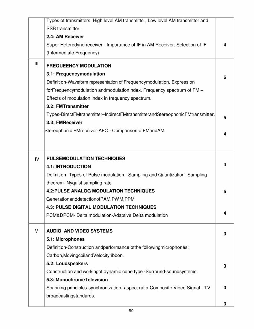
50
Types of transmitters: High level AM transmitter, Low level AM transmitter and
SSB transmitter.
2.4: AM Receiver
Super Heterodyne receiver - Importance of IF in AM Receiver. Selection of IF
(Intermediate Frequency)
4
III
FREQUEENCY MODULATION
3.1: Frequencymodulation
Definition-Waveform representation of Frequencymodulation, Expression
forFrequencymodulation andmodulationindex. Frequency spectrum of FM –
Effects of modulation index in frequency spectrum.
3.2: FMTransmitter
Types-DirectFMtransmitter–IndirectFMtransmitterandStereophonicFMtransmitter.
3.3: FMReceiver
Stereophonic FMreceiver-AFC - Comparison ofFMandAM.
6
5
4
IV PULSEMODULATION TECHNIQUES
4.1: INTRODUCTION
Definition- Types of Pulse modulation- Sampling and Quantization- Sampling
theorem- Nyquist sampling rate
4.2:PULSE ANALOG MODULATION TECHNIQUES
GenerationanddetectionofPAM,PWM,PPM
4.3: PULSE DIGITAL MODULATION TECHNIQUES
PCM&DPCM- Delta modulation-Adaptive Delta modulation
4
5
4
V
AUDIO AND VIDEO SYSTEMS
5.1: Microphones
Definition-Construction andperformance ofthe followingmicrophones:
Carbon,MovingcoilandVelocityribbon.
5.2: Loudspeakers
Construction and workingof dynamic cone type -Surround-soundsystems.
5.3: MonochromeTelevision
Scanning principles-synchronization -aspect ratio-Composite Video Signal - TV
broadcastingstandards.
3 3 3 3
51
5.4: ColorTV
Principlesofcolortransmissionandreception-Block diagram and working of PAL
Colour TV Receiver
5.5: DISPLAYS
Construction and working principle of LED ,OLED and Plasma display
2
REFERENCE BOOKS:
1. Networkslines and fields – John D.Ryder, PHI
2. Electronic communication Systems– Kennedy–TMH
3. Electronic Communication– Dennis RoddyandJohn colen– PHI
4. Fundamentals ofAcoustics–Kingsler&frey–WileyEastern ltd.
5. TV and Video engineering– Arvind M.Dhake – TMH.
6. CommunicationElectronics–Principlesandapplication–LouisEFrenzel, Third
Edition, Tata McGrawhillpublication
7. AudioandVideosystem–Principles,maintenanceandTroubleshooting byR.Gupta
Second Edition McGrawHill Education(P) Ltd.
52
STATE BOARD OF TECHNICAL EDUCATION &TRAINING, TAMILNADU
DIPLOMA IN ENGINEERING/TECHNOLOGY SYLLABUS
N SCHEME
(To be Implementedfor the students admitted from the year 2020 - 2021 onwards)
Course Name :1040:Electronics and Communication Engineering
Subject Code : 4040430
Semester :IV
Subject title : ANALOG AND DIGITAL ELECTRONICS
TEACHINGAND SCHEME OF EXAMINATION
No ofweeks/ semester: 16weeks
Subject
Instruction Examination
Hours
/Week
Hours
/Semester
Marks Duration Internal
Assessment
Board
Examination
Total
Analog and Digital
Electronics
4
64
25
100*
100
3 Hrs
* Examination will be conducted for 100 marks and it will be reduced to 75 marks.
Topics and Allocation of hours
Unit Topic Hrs
I Linear ICs and OP-amps 10
II A/D, D/A,Special Function ICs and IC Voltage Regulators 13
III Boolean Algebra and Arithmetic operations 10
IV Combinational and Sequential Logic Circuits 12
V Memories 12
Tests and Model Exam 7
Total 64
53
RATIONALE:
The subject Analog and Digital Electronics holds applications in all branches of
engineering instrumentation and Industrial Automation.Thiswillimpartindepth
knowledgeofNumber Systems , Logics of Combinational &Sequential circuits
and memories.
OBJECTIVES:
On completionofthefollowing units ofthe syllabus contents, the students must be able to
� Understand the basicsofoperational amplifier.
� Know the op-amp applications.
� Know the waveform generator and Active filter.
� Know the concept of D/A and A/D converters
� Know the applications of Special function IC, IC 555 Timer.
� Understand various Number Systems used in Digital Circuits
� Understand basic Boolean postulates and laws.
� Understand the De-Morgan’s theorem.
� Understand the concept ofKarnaugh Map.
� Learn about Basic logic Gates.
� Studyabout Boolean techniques.
� Learn the different digital logic families
� Learn arithmetic circuits- Adder/Subtractor
� Understand the encoder/decoder & MUX / DEMUX
� Understand the concept ofparityGeneratorand checker
� Understand various types of flip-flops.
� Understand various types ofcounters
� Understand various modes ofshift registers
� Understand various types of memories
54
4040430 ANALOG AND DIGITAL ELECTRONICS
DETAILED SYLLABUS
Contents: Theory Unit Name of the topics Hours
I
LINEAR ICS AND OP-AMPS
1.1: OPERATIONAL AMPLIFIER
Ideal Op-Amp – Block diagram and Characteristics – Op-amp parameters
CMRR – Slew rate – Concept of Virtual ground
1.2: APPLICATIONS OF OP-AMP
Inverting amplifier –Summing amplifier – Non inverting amplifier – Voltage
follower - Comparator – Zero crossing detector – Integrator – Differentiator-
waveform generation (SchmittTrigger only)–RC Low pass Active filter.
1.3: OP-AMP SPECIFICATIONS
OP-amp 741 – Symbol – Pin diagram – Specifications
4 4 2
II
A/D, D/A ,SPECIAL FUNCTION ICs AND IC VOLTAGE REGULATORS
2.1: SAMPLING AND QUANTIZATION
2.2: A/D CONVERTER
Analog to digitalconversion using Ramp method – Successive approximation
method – Dual slopemethod – Specifications of A/D converter
2.3: D/A CONVERTER
Basic concepts – Weighted Resistor D/A converter – R-2R Ladder
D/Aconverter – Specifications of DAC IC
2.4:SPECIAL FUNCTION ICs
2.4.1:IC555 Timer – Pin diagram - Functional Block diagram of IC 555 in
Astable and MonostableMultivibrator mode - Schmitt trigger using IC 555
2.4.2:IC 565-PLL-Pin diagram-Functional Block diagram of IC 565
2.4.3:IC 566-VCO-Pin diagram-Functional Block diagram of IC 566
2.5.: IC VOLTAGE REGULATORS
Positive IC Voltage Regulators: 78XX - Negative IC Voltage Regulators: 79XX
and General purpose IC Voltage Regulatorsusing LM 723.
2
3
2
3
3
55
III
BOOLEAN ALGEBRA AND ARITHMETIC OPERATIONS
3.1: NUMBER SYSTEMS
Decimal – Binary – Octal – Hexadecimal – BCD – Conversion from one
number system to other – Boolean Algebra – Basic laws and Demorgan’s
Theorems
3.2: UNIVERSAL GATES
Realization of basic logic gates using universal gates NAND and NOR -Tristate
Buffer circuit
3.3: PROBLEMS USING 2, 3, AND 4 VARIABLES
Boolean expression for outputs – Simplification of Boolean expression using
Karnaugh map (up to 4 variable)- Constructing logic circuits for the Boolean
expressions
3.4:ARITHMETIC OPERATIONS
Binary Addition-Binary Subtraction-1’s compliment and 2’s compliment-Signed
binary numbers
3.5: ARITHMETIC CIRCUITS
Half Adder-Full Adder-Half Subtractor-Full Subtractor
2
2
2
2
2
IV
COMBINATIONAL ANDSEQUENTIALLOGIC CIRCUITS
4.1: PARITY GENERATOR AND CHECKER
4.2: DECIMAL to BCD ENCODER
4.3: 3 to 8 DECODER
4.4: MULTIPLEXER: 4 to 1 Multiplexer
4.5: DEMULTIPLEXER :1 to 4 Demultiplexer 4.6: FLIP-FLOPS (FF)
RS FF– JK FF: Master Slave FF and Edge triggered FF – D and T FF
4.7: COUNTERS
4 bit Asynchronous Up Counter –Mod N counter – Decade counter –
4 bit Synchronous up counter
4.8:SHIFT REGISTER
4 bit shift register – Serial in Serial out
1
1
1
1
1
2
3
2
56
V
MEMORIES
5.1:CLASSIFICATION OF MEMORIES
5.2:RAM
RAMorganization-AddressLines and MemorySize- Read/writeoperations-Static
RAM-BipolarRAMcell- Dynamic RAM- SD RAM- DDR RAM.
5.3:ROM
ROM organization-Expanding memory- PROM- EPROM- and EEPROM- Flash
memory- Anti Fuse Technologies.
6
6
Reference books:
1. Albert Paul Malvino and Donold P. Leach – Digital Principles and Applications
2. Roger L. Tokheim Macmillan – Digital Electronics – McGraw – Hill –1994.
3. William H.Goth Mann – Digital Electronics – An introduction to theoryand practice –
PHI 1998.
4. Linear integrated circuits byB.Suseela&T.R.Ganeshbabu -Scitech publications-2018
5. Integrated circuits by K.R.Botkar-Khanna publisher’s-1996.
6.D.Roychoudhury&shail. B.Jain- Linear Integrated Circuits -New age International
publishers - II Edition -2004.
7.R.P.Jain – Modern Digital Electronics – TMH 2003.
57
STATE BOARD OF TECHNICAL EDUCATION &TRAINING, TAMILNADU
DIPLOMA IN ENGINEERING / TECHNOLOGY SYLLABUS
N-SCHEME
(To be Implementedfor the students admitted from the year 2020 - 2021 onwards)
Course Name : 1040:Electronics and Communication Engineering
Course Code : 4040440
Semester : IV Semester
Subject Title : INDUSTRIAL ELECTRONICS PRACTICAL
TEACHING AND SCHEME OF EXAMINATION No of weeks per semester: 16 weeks
Subject
Instructions Examination
Hours
/
Week
Hours /
Semester
Marks
Duration Internal
Assessment
Board
Examinations Total
INDUSTRIAL
ELECTRONICS
PRACTICAL
5 80 25 100* 100 3 Hrs.
* Examination will be conducted for 100 marks and it will be reduced to 75 marks.
RATIONALE:
The rationale behind the modifying this subject is to give clear explanation of power devices
and circuits that are widely used today in modern industry. It also gives exposure to PLCs
&Inverters which can perform various control functions in industrial environments.
OBJECTIVES:
� All the experiments given in the list of experiments should be completed and given for
the endSemester practical examination.
� In order to develop best skills in handling Instruments/Equipment and taking readings in
the practicalclasses, every three students should be provided with a separate
experimental setup for doingexperiments in the laboratory.
� The external examiners are requested to ensure that a single experimental question
should not begiven to more than three students while admitting a batch of 30 students
during Board Examinations.
58
4040440 INDUSTRIAL ELECTRONICS PRACTICAL
DETAILED SYLLABUS
Contents:Practical
Exercises
1. Phase control characteristics of SCR and testing a commutation circuit.
2. Construct a Lamp dimmer using TRIAC (in Bread Board Only)
3. Construct and test a MOSFET based PWM chopper circuit
4. Construct and test an IC based buck converter using PWM
5. Write and implement a simple ladder logic program using digital inputs and outputs for PLC
6. Write and implement a simple ladder logic program for interfacing a lift control with PLC.
7. Write and implement a simple ladder logic program for interfacing a conveyer control with
PLC.
8. Write and implement a simple ladder logic program using timer and counter with branching
and subroutines with PLC.
9. Construct and draw the VI characteristics of IGBT.
10. Construct and draw the VI characteristics of Power MOSFET.
11. Construct and draw single phase half controlled bridge converter with resistive load.
12. Construct and designa fan regulator using TRIAC and DIAC.
BOARD EXAMINATION
DETAILED ALLOCATION OF MARKS
CIRCUIT DIAGRAM : 25 CONNECTION : 25 EXECUTION & HANDLING OF EQUIPMENT : 25 OUTPUT / RESULT : 15 VIVA – VOCE :10 ________________________________________________________________
TOTAL : 100
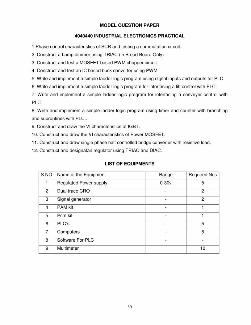
59
MODEL QUESTION PAPER
4040440 INDUSTRIAL ELECTRONICS PRACTICAL
1 Phase control characteristics of SCR and testing a commutation circuit.
2. Construct a Lamp dimmer using TRIAC (in Bread Board Only)
3. Construct and test a MOSFET based PWM chopper circuit
4. Construct and test an IC based buck converter using PWM
5. Write and implement a simple ladder logic program using digital inputs and outputs for PLC
6. Write and implement a simple ladder logic program for interfacing a lift control with PLC.
7. Write and implement a simple ladder logic program for interfacing a conveyer control with
PLC
8. Write and implement a simple ladder logic program using timer and counter with branching
and subroutines with PLC..
9. Construct and draw the VI characteristics of IGBT.
10. Construct and draw the VI characteristics of Power MOSFET.
11. Construct and draw single phase half controlled bridge converter with resistive load.
12. Construct and designafan regulator using TRIAC and DIAC.
LIST OF EQUIPMENTS
S.NO Name of the Equipment Range Required Nos
1 Regulated Power supply 0-30v 5
2 Dual trace CRO - 2
3 Signal generator - 2
4 PAM kit - 1
5 Pcm kit - 1
6 PLC’s - 5
7 Computers - 5
8 Software For PLC - -
9 Multimeter 10
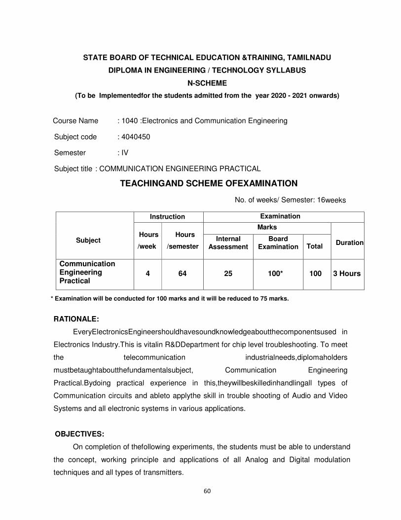
60
STATE BOARD OF TECHNICAL EDUCATION &TRAINING, TAMILNADU
DIPLOMA IN ENGINEERING / TECHNOLOGY SYLLABUS
N-SCHEME
(To be Implementedfor the students admitted from the year 2020 - 2021 onwards)
Course Name : 1040 :Electronics and Communication Engineering
Subject code : 4040450 Semester : IV
Subject title : COMMUNICATION ENGINEERING PRACTICAL
TEACHINGAND SCHEME OFEXAMINATION
No. of weeks/ Semester: 16weeks
Subject
Instruction Examination
Hours
/week
Hours
/semester
Marks Duration
Internal Assessment
Board Examination
Total
Communication Engineering Practical
4
64
25
100*
100
3 Hours
* Examination will be conducted for 100 marks and it will be reduced to 75 marks.
RATIONALE:
EveryElectronicsEngineershouldhavesoundknowledgeaboutthecomponentsused in
Electronics Industry.This is vitalin R&DDepartment for chip level troubleshooting. To meet
the telecommunication industrialneeds,diplomaholders
mustbetaughtaboutthefundamentalsubject, Communication Engineering
Practical.Bydoing practical experience in this,theywillbeskilledinhandlingall types of
Communication circuits and ableto applythe skill in trouble shooting of Audio and Video
Systems and all electronic systems in various applications.
OBJECTIVES:
On completion of thefollowing experiments, the students must be able to understand
the concept, working principle and applications of all Analog and Digital modulation
techniques and all types of transmitters.
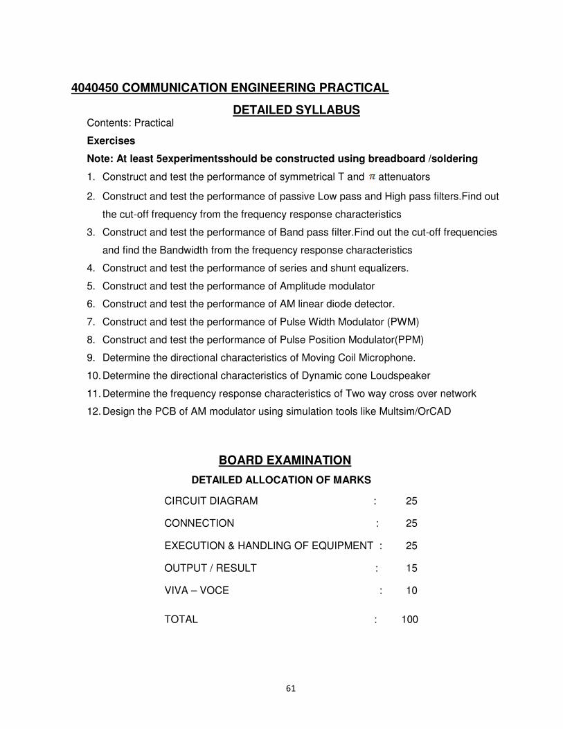
61
4040450 COMMUNICATION ENGINEERING PRACTICAL
DETAILED SYLLABUS Contents: Practical
Exercises
Note: At least 5experimentsshould be constructed using breadboard /soldering
1. Construct and test the performance of symmetrical T and attenuators
2. Construct and test the performance of passive Low pass and High pass filters.Find out
the cut-off frequency from the frequency response characteristics
3. Construct and test the performance of Band pass filter.Find out the cut-off frequencies
and find the Bandwidth from the frequency response characteristics
4. Construct and test the performance of series and shunt equalizers.
5. Construct and test the performance of Amplitude modulator
6. Construct and test the performance of AM linear diode detector.
7. Construct and test the performance of Pulse Width Modulator (PWM)
8. Construct and test the performance of Pulse Position Modulator(PPM)
9. Determine the directional characteristics of Moving Coil Microphone.
10. Determine the directional characteristics of Dynamic cone Loudspeaker
11. Determine the frequency response characteristics of Two way cross over network
12. Design the PCB of AM modulator using simulation tools like Multsim/OrCAD
BOARD EXAMINATION
DETAILED ALLOCATION OF MARKS
CIRCUIT DIAGRAM : 25 CONNECTION :
25
EXECUTION & HANDLING OF EQUIPMENT :
25
OUTPUT / RESULT :
15
VIVA – VOCE :
10
TOTAL : 100
62
MODEL QUESTION PAPER
4040450COMMUNICATION ENGINEERING PRACTICAL
Note: At least 5 experiments should be done using Soldering board / Bread board
1. Construct and test the performance of symmetrical T and attenuators
2. Construct and test the performance of passive Low pass and High pass filters. Find out
the cut-off frequency from the frequency response characteristics
3. Construct and test the performance of Band pass filter.Find out the cut-off frequencies
and find the Bandwidth from the frequency response characteristics
4. Construct and test the performance of series and shunt equalizers.
5. Construct and test the performance of Amplitude modulator
6. Construct and test the performance of AM linear diode detector.
7. Construct and test the performance of Pulse Width Modulator (PWM)
8. Construct and test the performance of Pulse Position Modulator(PPM)
9. Determine the directional characteristics of Moving Coil Microphone.
10. Determine the directional characteristics of Dynamic cone Loudspeaker
11. Determine the frequency response characteristics of Two way cross over network
12. Design the PCB of AM modulator simulation tools like Multsim /OrCAD
LIST OF EQUIPMENTS
S.NO Name of the Equipment Range Required No.
1. Regulated Power Supply 0 – 30V 10
2. Dual trace CRO 60 MHz 5
3. Signal Generator - 10
4. Desk Top Computer - 2
5. Decade Resistance Box 0 - 100KOhm 5
6. Decade Capacitance Box 0 - 100uF 5
7. Decade Inductance Box 0 - 10H 5
8. Dynamic cone Loud speaker - 2
9. Moving coil Microphone - 1
10. Velocity Ribbon Micro phone - 1
11. Software Tool Multisim/OrCAD
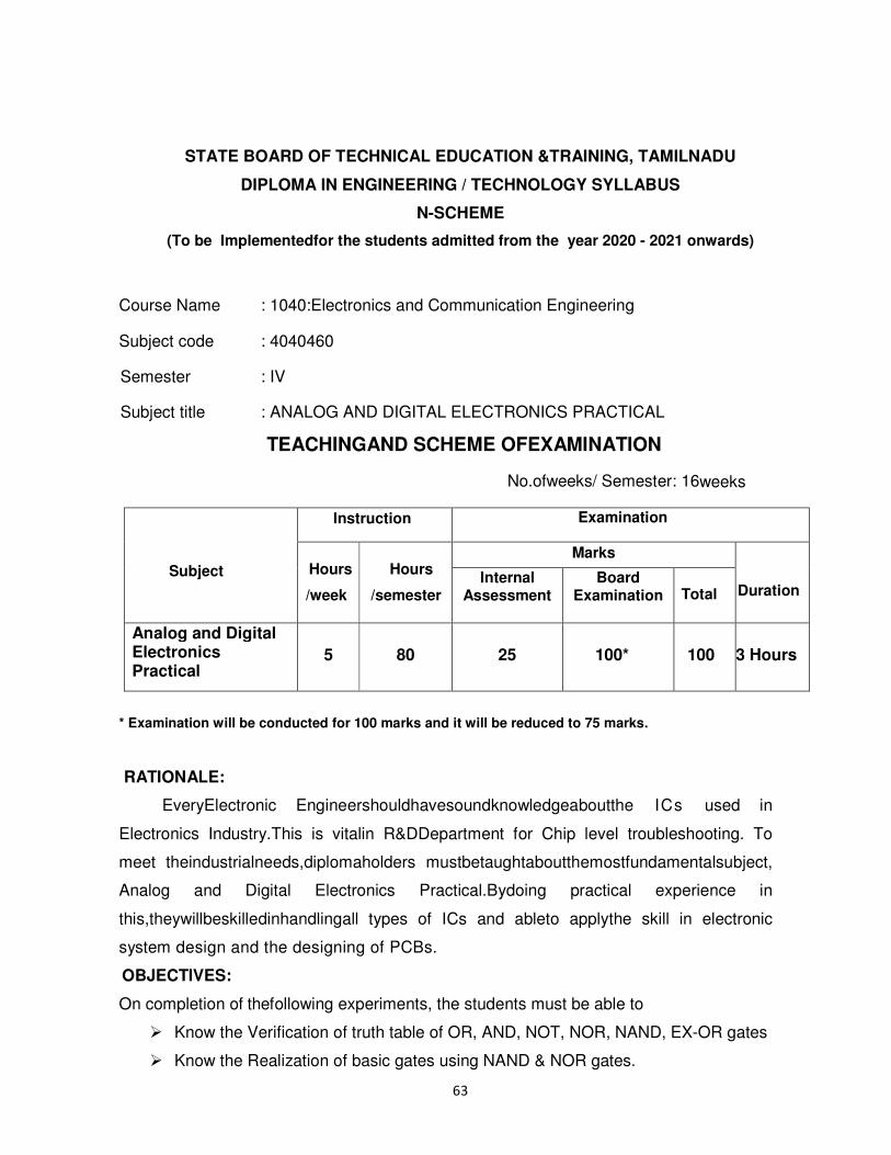
63
STATE BOARD OF TECHNICAL EDUCATION &TRAINING, TAMILNADU
DIPLOMA IN ENGINEERING / TECHNOLOGY SYLLABUS
N-SCHEME
(To be Implementedfor the students admitted from the year 2020 - 2021 onwards)
Course Name : 1040:Electronics and Communication Engineering
Subject code : 4040460 Semester : IV
Subject title : ANALOG AND DIGITAL ELECTRONICS PRACTICAL
TEACHINGAND SCHEME OFEXAMINATION
No.ofweeks/ Semester: 16weeks
Subject
Instruction Examination
Hours
/week
Hours
/semester
Marks Duration
Internal Assessment
Board Examination
Total
Analog and Digital Electronics Practical
5
80
25
100*
100
3 Hours
* Examination will be conducted for 100 marks and it will be reduced to 75 marks.
RATIONALE:
EveryElectronic Engineershouldhavesoundknowledgeaboutthe ICs used in
Electronics Industry.This is vitalin R&DDepartment for Chip level troubleshooting. To
meet theindustrialneeds,diplomaholders mustbetaughtaboutthemostfundamentalsubject,
Analog and Digital Electronics Practical.Bydoing practical experience in
this,theywillbeskilledinhandlingall types of ICs and ableto applythe skill in electronic
system design and the designing of PCBs.
OBJECTIVES:
On completion of thefollowing experiments, the students must be able to
� Know the Verification of truth table of OR, AND, NOT, NOR, NAND, EX-OR gates
� Know the Realization of basic gates using NAND & NOR gates.
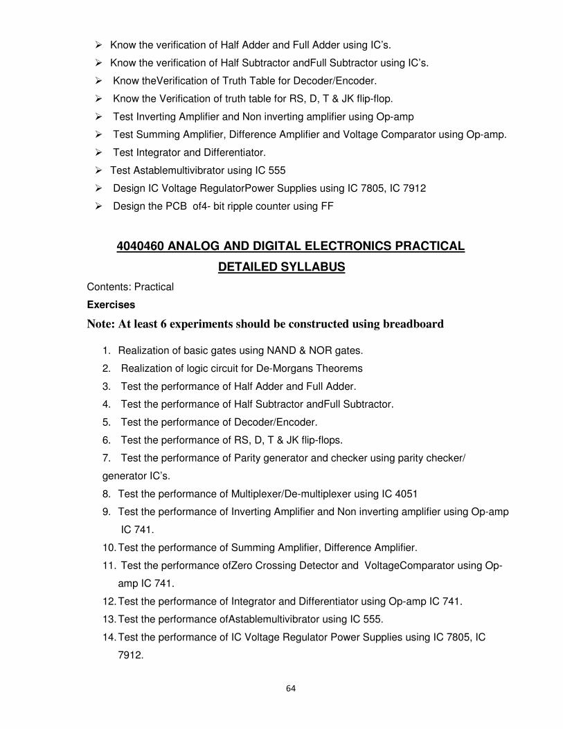
64
� Know the verification of Half Adder and Full Adder using IC’s.
� Know the verification of Half Subtractor andFull Subtractor using IC’s.
� Know theVerification of Truth Table for Decoder/Encoder.
� Know the Verification of truth table for RS, D, T & JK flip-flop.
� Test Inverting Amplifier and Non inverting amplifier using Op-amp
� Test Summing Amplifier, Difference Amplifier and Voltage Comparator using Op-amp.
� Test Integrator and Differentiator.
� Test Astablemultivibrator using IC 555
� Design IC Voltage RegulatorPower Supplies using IC 7805, IC 7912
� Design the PCB of4- bit ripple counter using FF
4040460 ANALOG AND DIGITAL ELECTRONICS PRACTICAL
DETAILED SYLLABUS
Contents: Practical
Exercises
Note: At least 6 experiments should be constructed using breadboard
1. Realization of basic gates using NAND & NOR gates.
2. Realization of logic circuit for De-Morgans Theorems
3. Test the performance of Half Adder and Full Adder.
4. Test the performance of Half Subtractor andFull Subtractor.
5. Test the performance of Decoder/Encoder.
6. Test the performance of RS, D, T & JK flip-flops.
7. Test the performance of Parity generator and checker using parity checker/
generator IC’s.
8. Test the performance of Multiplexer/De-multiplexer using IC 4051
9. Test the performance of Inverting Amplifier and Non inverting amplifier using Op-amp
IC 741.
10. Test the performance of Summing Amplifier, Difference Amplifier.
11. Test the performance ofZero Crossing Detector and VoltageComparator using Op-
amp IC 741.
12. Test the performance of Integrator and Differentiator using Op-amp IC 741.
13. Test the performance ofAstablemultivibrator using IC 555.
14. Test the performance of IC Voltage Regulator Power Supplies using IC 7805, IC
7912.
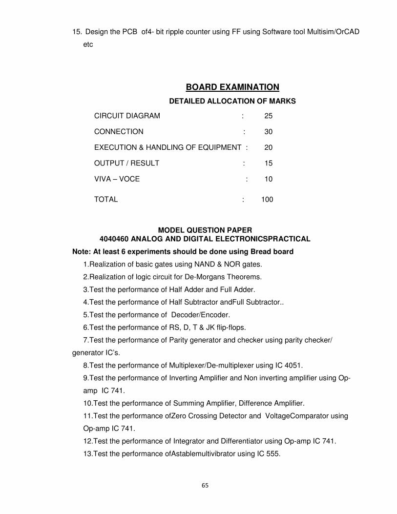
65
15. Design the PCB of4- bit ripple counter using FF using Software tool Multisim/OrCAD
etc
BOARD EXAMINATION
DETAILED ALLOCATION OF MARKS
CIRCUIT DIAGRAM : 25 CONNECTION :
30
EXECUTION & HANDLING OF EQUIPMENT :
20
OUTPUT / RESULT :
15
VIVA – VOCE :
10
TOTAL : 100
MODEL QUESTION PAPER
4040460 ANALOG AND DIGITAL ELECTRONICSPRACTICAL
Note: At least 6 experiments should be done using Bread board
1.Realization of basic gates using NAND & NOR gates.
2.Realization of logic circuit for De-Morgans Theorems.
3.Test the performance of Half Adder and Full Adder.
4.Test the performance of Half Subtractor andFull Subtractor..
5.Test the performance of Decoder/Encoder.
6.Test the performance of RS, D, T & JK flip-flops.
7.Test the performance of Parity generator and checker using parity checker/
generator IC’s.
8.Test the performance of Multiplexer/De-multiplexer using IC 4051.
9.Test the performance of Inverting Amplifier and Non inverting amplifier using Op-
amp IC 741.
10.Test the performance of Summing Amplifier, Difference Amplifier.
11.Test the performance ofZero Crossing Detector and VoltageComparator using
Op-amp IC 741.
12.Test the performance of Integrator and Differentiator using Op-amp IC 741.
13.Test the performance ofAstablemultivibrator using IC 555.
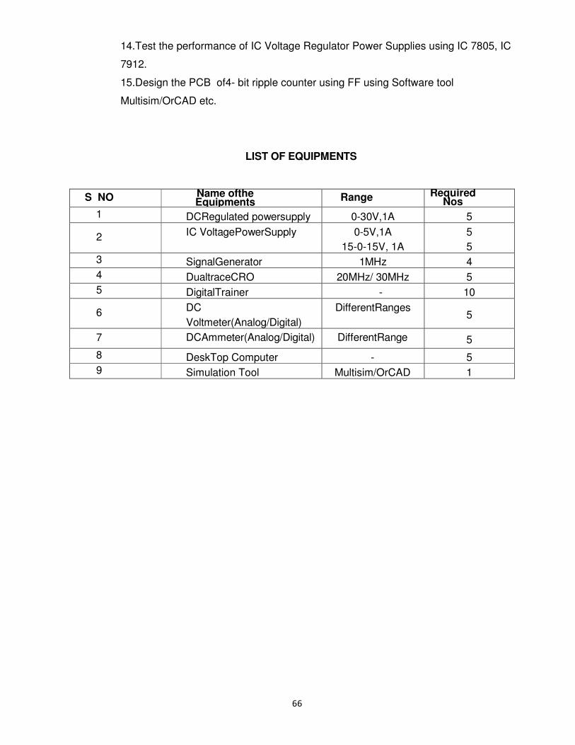
66
14.Test the performance of IC Voltage Regulator Power Supplies using IC 7805, IC
7912.
15.Design the PCB of4- bit ripple counter using FF using Software tool
Multisim/OrCAD etc.
LIST OF EQUIPMENTS
S NO Name ofthe Equipments Range Required
Nos 1 DCRegulated powersupply 0-30V,1A 5
2 IC VoltagePowerSupply 0-5V,1A
15-0-15V, 1A
5
5
3 SignalGenerator 1MHz 4
4 DualtraceCRO 20MHz/ 30MHz 5
5 DigitalTrainer - 10
6 DC
Voltmeter(Analog/Digital)
DifferentRanges 5
7 DCAmmeter(Analog/Digital) DifferentRange 5
8 DeskTop Computer - 5
9 Simulation Tool Multisim/OrCAD 1
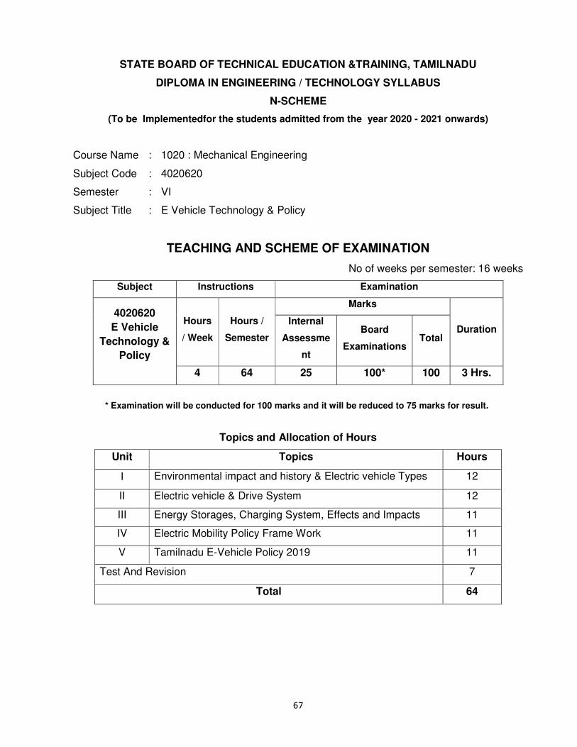
67
STATE BOARD OF TECHNICAL EDUCATION &TRAINING, TAMILNADU
DIPLOMA IN ENGINEERING / TECHNOLOGY SYLLABUS
N-SCHEME
(To be Implementedfor the students admitted from the year 2020 - 2021 onwards)
Course Name : 1020 : Mechanical Engineering
Subject Code : 4020620
Semester : VI
Subject Title : E Vehicle Technology & Policy
TEACHING AND SCHEME OF EXAMINATION
No of weeks per semester: 16 weeks
Subject Instructions Examination
4020620
E Vehicle
Technology &
Policy
Hours
/ Week
Hours /
Semester
Marks
Duration Internal
Assessme
nt
Board
Examinations Total
4 64 25 100* 100 3 Hrs.
* Examination will be conducted for 100 marks and it will be reduced to 75 marks for result.
Topics and Allocation of Hours
Unit Topics Hours
I Environmental impact and history & Electric vehicle Types 12
II Electric vehicle & Drive System 12
III Energy Storages, Charging System, Effects and Impacts 11
IV Electric Mobility Policy Frame Work 11
V Tamilnadu E-Vehicle Policy 2019 11
Test And Revision 7
Total 64
68
RATIONALE:
The world is transitioning to cleaner mobility options with the aim at improving air quality and
reducing dependency on fossil fuels. Electric Vehicles (EVs) have emerged a popular clean
mobility choice to reduce emissions. EVs are powered fully or partially by batteries, they can
help to reduce dependence on fossil fuels also air quality. Tamil Nadu is one of the most
advanced states in India. Tamil Nadu has a highly developed industrial eco-system and is very
strong in sectors like automobiles and auto-components. Many globally renowned companies
have setup their manufacturing facilities in Tamil Nadu. Due the rapid depletion of fossil fuel
and increase in fuel cost, environmental pollution, the shift to clean transport is necessary. This
subject introduced by keeping all the above factors.
OBJECTIVES:
• To learn the environmental impact and history of Electric Vehicles.
• To understand the concept of Electric Vehicle and its types.
• To study the configurations of Electric Vehicles
• To acquire knowledge about Energy Storages, Charging System, Effects and Impacts
• To appreciate the Electric Mobility Policy Frame work India and EV Policy Tamil Nadu
2019.
69
4020620 E Vehicle Technology & Policy
DETAILED SYLLABUS
Contents: Theory
Unit Name of the Topics Hours
I Environmental impact and history:
Environmental impact of conventional vehicle - Air pollution – Petroleum
resources – History of Electric vehicles & Hybrid Electric Vehicles -
Conventional drive train system – Rear Wheel, Front Wheel and All
wheel - Parts of Drive train system
Electric vehicle Types:
Introduction to Battery Electric Vehicle (BEV) – Definition BEV –
Necessity BEV – Different between BEV and Conventional Vehicle -
Advantages of BEV - Block diagram of BEV – Hybrid electric Vehicle
(HEV) - Plug-in Hybrid Electric Vehicle (PHEV) – Fuel Cell Electric
Vehicle (FCEV) – Description.
12
II Electric Vehicles:
Configurations of Electric Vehicle – Performance of Electric Vehicles –
Tractive Effort in Normal Driving – energy consumption.
Hybrid Electric Vehicles: Concept of Hybrid electric drive trains –
Architecture of Hybrid Electric Drive trains – Series, Parallel and Series &
Parallel
Electric Propulsion Systems:
Types of EV motors - DC motor drives– Permanent Magnetic Brush Less
DC Motor Drives (BLDC) – Principles, Construction and Working – Hub
motor Drive system – Merits and Demerits of DC motor drive, BLDC
motor drive
12
III Energy Storages:
Electrochemical Batteries – Battery Technologies – Construction and
working of Lead Acid Batteries, Nickel Based Batteries and Lithium
Based Batteries Role of Battery Management System (BMS)– Battery
pack development Technology– Cell Series and Parallel connection to
develop battery pack.
Charging:
11
70
Battery Charging techniques - Constant current and Constant voltage,
Trickle charging – Battery Swapping Techniques – DC charging –
Wireless charging – Maintenance of Battery pack – Latest development
in battery chemistry.
Effects and Impacts:
Effects of EV – Impacts on Power grid – Impacts on Environment –
Impacts on Economy.
IV Electric Mobility Policy Frame Work
Government of India Electric Mobility Policy Frame work – Global
Scenario of EV adoption – Electric mobility in India – National Electric
Mobility Mission Plan 2020 – Action led by Original Equipment
Manufacturers – Need of EV Policy – Advantage of EV Eco system –
Scope and Applicability of EV Policy – ARAI Standards for Electric
Vehicle – AIS 038, AIS 039 &AIS 123 - Key Performance Indicator -
Global impact – Trends and Future Developments
11
V Tamil Nadu E-Vehicle Policy 2019
Tamil Nadu E-vehicle Policy 2019: Vehicle Population in Tamil Nadu –
Objectives of EV Policy – Policy Measures – Demand side incentives –
Supply side incentives to promote EV manufacturing – Revision of
Transport Regulation of EV – City building codes – Capacity Building and
Skilling – Charging structure – implementing agencies – R&D and
Business Incubation – Recycling Ecosystem – Battery and EVs
11
Reference Books
1. Modern Electric, Hybrid Electric and Fuel Cell Vehicles, Mehrdad Ehsani, Yimin Gao,
Sebastien E.Gay, Ali Emadi, CR Press, London, New York.
2. Comparison of Electric and Conventional Vehicles in Indian Market: Total Cost of
Ownership, Consumer Preference and Best Segment for Electric Vehicle (IJSR), Akshat
Bansal, Akriti Agarwal
3. A Comprehensive Study of Key Electric Vehicle (EV) Components, Technologies,
Challenges, Impacts, and Future Direction of Development (MDPI), Fuad Un-Noor,
SanjeevikumarPadmanaban, Lucian Mihet-Popa, Mohammad NurunnabiMollah and
Eklas Hossain.
4. Electric Vehicles: A future Projection CII October 2020 report.
5. Design and analysis of aluminum/air battery system for electric vehicles, Shaohua Yang,
Harold Knickle, Elsevier.
71
6. Propelling Electric Vehicles in India, Technical study of Electric Vehicles and Charging
Infrastructure
7. ZERO EMISSION VEHICLES (ZEVs): TOWARDS A POLICY FRAMEWORK – NTI
Aayog.
8. FASTER ADOPTION OF ELECTRIC VEHICLES IN INDIA: PERSPECTIVE OF
CONSUMERS AND INDUSTRY, The Energy and Resources Institute, New Delhi.
9. India EV Story: Emerging Opportunities by Innovation Norway.
10. Automotive Industry Standards – AIS 038, AIS 039 & AIS 123 – Manual
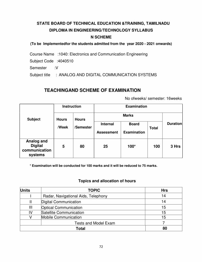
72
STATE BOARD OF TECHNICAL EDUCATION &TRAINING, TAMILNADU
DIPLOMA IN ENGINEERING/TECHNOLOGY SYLLABUS
N SCHEME
(To be Implementedfor the students admitted from the year 2020 - 2021 onwards)
Course Name :1040: Electronics and Communication Engineering
Subject Code :4040510
Semester :V
Subject title : ANALOG AND DIGITAL COMMUNICATION SYSTEMS
TEACHINGAND SCHEME OF EXAMINATION
No ofweeks/ semester: 16weeks
Subject
Instruction Examination
Hours
/Week
Hours
/Semester
Marks Duration Internal
Assessment
Board
Examination
Total
Analog and Digital
communication systems
5
80
25
100*
100
3 Hrs
* Examination will be conducted for 100 marks and it will be reduced to 75 marks.
Topics and allocation of hours
Units TOPIC Hrs
I Radar, Navigational Aids, Telephony 14
II Digital Communication 14
III Optical Communication 15
IV Satellite Communication 15
V Mobile Communication 15
Tests and Model Exam 7
Total 80
73
RATIONALE:
The subject Analog and Digital communication systems will enable the
students to learn about the advancement in communication systems. it will give
exposure to the various modes of communication viz Radar, Telephone, digital
communication, digital codes, optical communication, satellite communication,
microwave communication, mobile communication and satellite multiple access
techniques.
OBJECTIVES:
On completionofthefollowing units ofthe syllabus contents, the students must be able
� To understand principles of Radar.
� To understand principles of navigational aids .
� To study Electronic Exchange .
� To study basic digital communication system and discuss the characteristics
of data transmission circuits.
� To learn Error detection and correction codes and various digital modulation
techniques
� To learn optical sources, optical detectors.
� To discuss the applications of fiber optic communication
� To Study satellite system, orbits, launching, Antennas
� To Study earth segment and space segment components
� To study about satellite services
� To study fundamental cellular concepts such as frequency reuse, handoff.
� To learn multiple access techniques.
� To learn digital cellular system-GSM
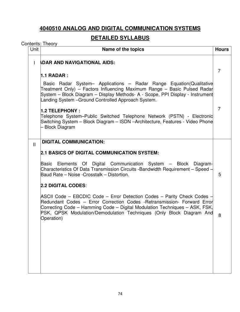
74
4040510 ANALOG AND DIGITAL COMMUNICATION SYSTEMS
DETAILED SYLLABUS Contents: Theory
Unit Name of the topics Hours
I
RADAR AND NAVIGATIONAL AIDS:
11.1 RADAR :
Basic Radar System– Applications – Radar Range Equation(Qualitative Treatment Only) – Factors Influencing Maximum Range – Basic Pulsed Radar System – Block Diagram – Display Methods- A - Scope, PPI Display - Instrument Landing System –Ground Controlled Approach System. 1.2 TELEPHONY : Telephone System–Public Switched Telephone Network (PSTN) - Electronic Switching System – Block Diagram – ISDN –Architecture, Features - Video Phone – Block Diagram
7 7
II
DIGITAL COMMUNICATION:
2.1 BASICS OF DIGITAL COMMUNICATION SYSTEM:
Basic Elements Of Digital Communication System – Block Diagram-Characteristics Of Data Transmission Circuits -Bandwidth Requirement – Speed –Baud Rate – Noise -Crosstalk – Distortion.
2.2 DIGITAL CODES: ASCII Code – EBCDIC Code – Error Detection Codes – Parity Check Codes –Redundant Codes – Error Correction Codes -Retransmission- Forward Error Correcting Code – Hamming Code – Digital Modulation Techniques – ASK, FSK, PSK, QPSK Modulation/Demodulation Techniques (Only Block Diagram And Operation)
5
8
75
III
OPTICAL COMMUNICATION : 3.1 BASICS OF OPTICAL COMMUNICATION AND LOSSES: Optical Communication System – Block Diagram – Advantages Of Optical Fiber Communication Systems – Principles Of Light Transmission In A Fiber Using Ray Theory – Single Mode Fibers, Multimode Fibers – Step Index Fibers, Graded Index Fibers (Basic Concepts Only) – Attenuation In Optical Fibers -Absorption Losses, Scattering Losses, Bending Losses, Core And Cladding Losses 3.2 OPTICAL SOURCES AND APPLICATIONS:
Optical Sources – LED – Semiconductor LASER – Principles – Optical Detectors –PIN And APD Diodes - Optical Transmitter – Block Diagram – Optical Receiver –Block Diagram – Application Of Optical Fibers – Networking, Industry And Military Applications.
7
7
IV
SATELLITE COMMUNICATION:
4.1SATELLITE SYSTEM:
Kepler’s I,II,II laws – orbits – launching orbits – types - Geostationary synchronous satellites - Advantages – Apogee – Perigee - Active and passive satellite - Earth eclipse of satellite
4.2ANTENNA:
Parabolic reflector antenna
4.3SPACE SEGMENT:
Space segment: Power supply- Attitude control- station keeping – Transponders –TT and C subsystem – Antenna subsystem.
4.4 EARTH SEGMENT:
Earth segment: Block diagram of Transmit receive earth station - Satellite mobile services - Basics of GPS.
4.4 MICROWAVE COMMUNICATION:
Microwave frequency ranges - microwave devices – Parametric amplifiers –Travelling wave tubes – simple block diagram of microwave transmitter, receiver
4
1
3
3
4
76
and microwave link repeater
V
MOBILE COMMUNICATION AND MUTIPLE ACCESS TECHNIQUES:
5.1MOBILE COMMUNICATION: (Qualitative Treatment only)
Cellular telephone– fundamental concepts – Simplified Cellular telephone system - frequency reuse – Interference – Co-channel Interference – Adjacent Channel Interference – Improving coverage and capacity in cellular systems –
cell splitting – sectoring – Roaming and Handoff – Basics of blue tooth technology
5.2SATELLITE MULTIPLE ACCESS TECHNIQUES:
TDMA, FDMA, CDMA. Digital cellular system – Global system for mobile communications (GSM) –GSM services – GSM System Architecture – Basics of GPRS.
7
7
Reference Books:
1. Electronic communication systems - Kennedy - Davis - fourth Edition – Tata McGraw Hill - 1999.
2. Electronics communication - Dennis Roddy and John coolen – Third Edition - PHI – 1988
3. Optical fiber communication - Gerd Keiser - Third Edition - McGraw Hill – 2000
4. Satellite communication - Dr. D.C. Agarwal - Third Edition –Khannapublishers– 1995
5. Satellite communication - Dennis Roddy - Third Edition - McGraw Hill – 2001
6. Electronic communication systems-Fundamentals through Advanced –Wayne Tomasi-fifth Edition –pearson Education-2005
77
STATE BOARD OF TECHNICAL EDUCATION &TRAINING, TAMILNADU
DIPLOMA IN ENGINEERING / TECHNOLOGY SYLLABUS
N-SCHEME
(To be Implemented for the students admitted from the year 2020 - 2021 onwards)
Course Name : 1040: Electronics and Communication Engineering Subject Code : 4040520
Semester : V
Subject Title : Microcontroller and its applications
TEACHING AND SCHEME OF EXAMINATION
No of weeks per semester: 16 weeks
Subject
Instructions Examination
Hours /
Week
Hours /
Semester
Marks
Duration Internal
Assessment
Board
Examinations Total
Microcontroller
and its
Applications
5 80 25 100* 100 3 Hrs.
* Examination will be conducted for 100 marks and it will be reduced to 75 marks.
Topics and Allocation of Hours
UNIT Topic Hrs.
I Architecture of 8051 Microcontroller 15
II 8051 Instruction set and Programming 16
III Peripherals of 8051 15
IV Interfacing techniques 16
V Advanced Microcontrollers 11
Test & Model Exam 7
Total 80
78
RATIONALE:
The introduction of this subject will enable the students to learn about microcontroller
8051 architecture, Pin details, Instruction sets, Programming and interfacing. This subject
enables the students to do the project effectively. It also helps the students to choose the field
of interest. If the student is aiming for higher studies, this subject is foundation.
OBJECTIVES:
On completion of the syllabus, the students must be able to
-> Know the difference between microprocessor and microcontroller.
-> Understand the architecture of 8051.
-> Write programs using 8051 ALP.
-> Understand the programming of I/O ports, Timer, Interrupt and Serial Programming.
-> Use the interfacing techniques
-> Know the types of microcontrollers
-> Explain IoT.
.
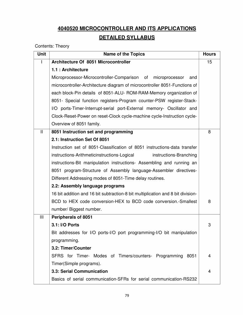
79
4040520 MICROCONTROLLER AND ITS APPLICATIONS
DETAILED SYLLABUS
Contents: Theory
Unit Name of the Topics Hours
I Architecture Of 8051 Microcontroller
1.1 : Architecture
Microprocessor-Microcontroller-Comparison of microprocessor and
microcontroller-Architecture diagram of microcontroller 8051-Functions of
each block-Pin details of 8051-ALU- ROM-RAM-Memory organization of
8051- Special function registers-Program counter-PSW register-Stack-
I/O ports-Timer-Interrupt-serial port-External memory- Oscillator and
Clock-Reset-Power on reset-Clock cycle-machine cycle-Instruction cycle-
Overview of 8051 family.
15
II 8051 Instruction set and programming
2.1: Instruction Set Of 8051
Instruction set of 8051-Classification of 8051 instructions-data transfer
instructions-Arithmeticinstructions-Logical instructions-Branching
instructions-Bit manipulation instructions- Assembling and running an
8051 program-Structure of Assembly language-Assembler directives-
Different Addressing modes of 8051-Time delay routines.
2.2: Assembly language programs
16 bit addition and 16 bit subtraction-8 bit multiplication and 8 bit division-
BCD to HEX code conversion-HEX to BCD code conversion.-Smallest
number/ Biggest number.
8
8
III Peripherals of 8051
3.1: I/O Ports
Bit addresses for I/O ports-I/O port programming-I/O bit manipulation
programming.
3.2: Timer/Counter
SFRS for Timer- Modes of Timers/counters- Programming 8051
Timer(Simple programs).
3.3: Serial Communication
Basics of serial communication-SFRs for serial communication-RS232
3
4
4
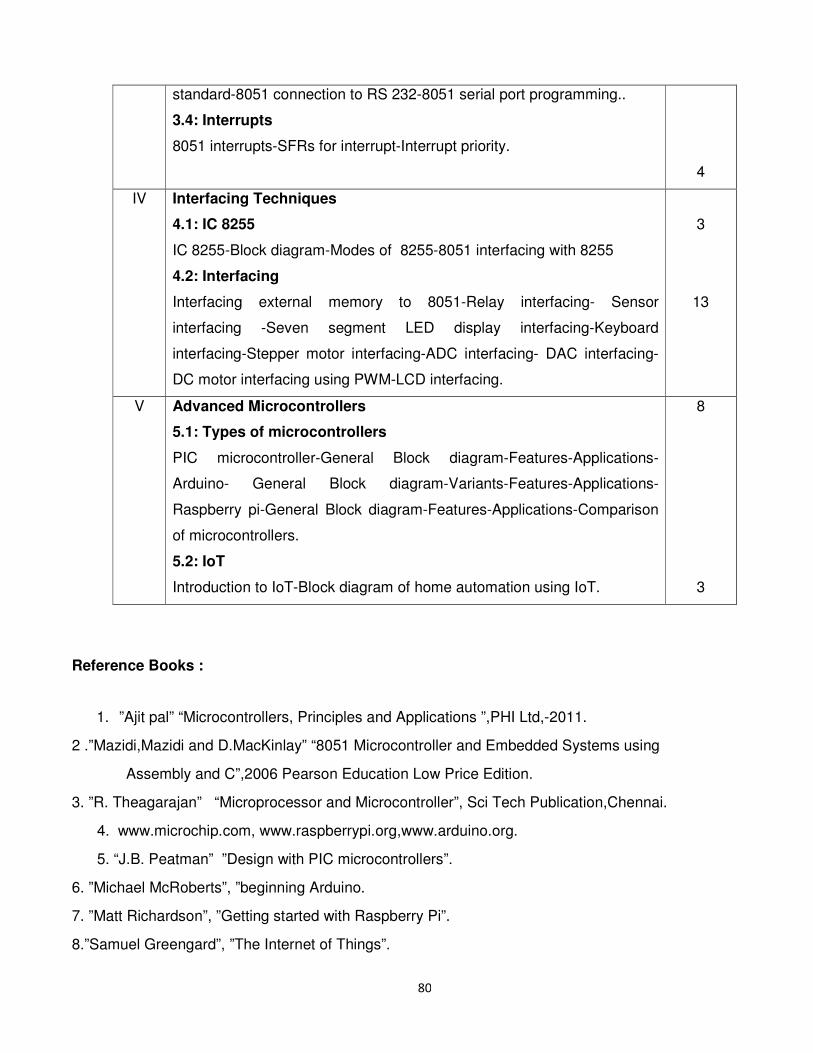
80
standard-8051 connection to RS 232-8051 serial port programming..
3.4: Interrupts
8051 interrupts-SFRs for interrupt-Interrupt priority.
4
IV Interfacing Techniques
4.1: IC 8255
IC 8255-Block diagram-Modes of 8255-8051 interfacing with 8255
4.2: Interfacing
Interfacing external memory to 8051-Relay interfacing- Sensor
interfacing -Seven segment LED display interfacing-Keyboard
interfacing-Stepper motor interfacing-ADC interfacing- DAC interfacing-
DC motor interfacing using PWM-LCD interfacing.
3
13
V Advanced Microcontrollers
5.1: Types of microcontrollers
PIC microcontroller-General Block diagram-Features-Applications-
Arduino- General Block diagram-Variants-Features-Applications-
Raspberry pi-General Block diagram-Features-Applications-Comparison
of microcontrollers.
5.2: IoT
Introduction to IoT-Block diagram of home automation using IoT.
8
3
Reference Books :
1. ”Ajit pal” “Microcontrollers, Principles and Applications ”,PHI Ltd,-2011.
2 .”Mazidi,Mazidi and D.MacKinlay” “8051 Microcontroller and Embedded Systems using
Assembly and C”,2006 Pearson Education Low Price Edition.
3. ”R. Theagarajan” “Microprocessor and Microcontroller”, Sci Tech Publication,Chennai.
4. www.microchip.com, www.raspberrypi.org,www.arduino.org.
5. “J.B. Peatman” ”Design with PIC microcontrollers”.
6. ”Michael McRoberts”, ”beginning Arduino.
7. ”Matt Richardson”, ”Getting started with Raspberry Pi”.
8.”Samuel Greengard”, ”The Internet of Things”.
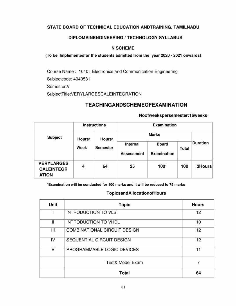
81
STATE BOARD OF TECHNICAL EDUCATION ANDTRAINING, TAMILNADU
DIPLOMAINENGINEERING / TECHNOLOGY SYLLABUS
N SCHEME
(To be Implementedfor the students admitted from the year 2020 - 2021 onwards)
Course Name : 1040: Electronics and Communication Engineering
Subjectcode: 4040531
Semester:V
SubjectTitle:VERYLARGESCALEINTEGRATION
TEACHINGANDSCHEMEOFEXAMINATION
Noofweekspersemester:16weeks
Subject
Instructions Examination
Hours/
Week
Hours/
Semester
Marks
Duration Internal
Assessment
Board
Examination
Total
VERYLARGES
CALEINTEGR
ATION
4 64 25 100* 100 3Hours
*Examination will be conducted for 100 marks and it will be reduced to 75 marks
TopicsandAllocationofHours
Unit Topic Hours
I INTRODUCTION TO VLSI 12
II INTRODUCTION TO VHDL 10
III COMBINATIONAL CIRCUIT DESIGN 12
IV SEQUENTIAL CIRCUIT DESIGN 12
V PROGRAMMABLE LOGIC DEVICES 11
Test& Model Exam 7
Total 64
82
RATIONALE:
Very Large Scale Integration technology, when especially used fordesigning digital
systems, it is mandatory that thebehaviorof therequired system to be described (modeled) and
verified (simulated)before synthesis, translate the design into real hardware fabricationin the
foundry (gates and wires).Hardware DescriptionLanguage (HDL)allows designs to be described
using any methodology- top down,bottomup approach. VHDLcan be used to describe hardware
atthe gatelevel or in a more abstract way. This course is to introduce the digital system design
conceptsthrough hardware descriptionLanguage,VHDL programming, design flow of VLSI
andarchitectures ofCPLD, FPGA.Itis mainlyaimedatdesignofcombinational
andsequentialfunctions and simulates or
verifiestheirfunctionalityusingtheHardwaredescriptionLanguage(HDL).
OBJECTIVES:
Onsuccessfulcompletionofthecourse,thestudentsmustbeableto
� Understand the concepts of VLSIdesignprocess.
� DevelopaVHDLcodeforcombinationalcircuit
� DevelopaVHDLcodeforsequentialcircuit.
� ExplaintheimportanceofPROM,PLA,and PAL.
� DifferentiatePROM, PLAandPAL.
� Developthecircuitusing PROM, PALandPLA.
� Understand CPLDandFPGAhardware.
� Differentiate ASIC, CPLD, FPGA.
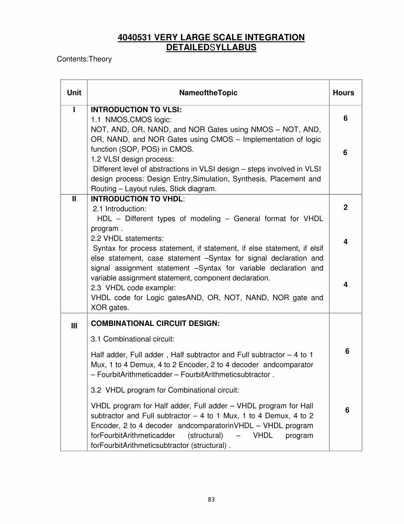
83
4040531 VERY LARGE SCALE INTEGRATION DETAILEDSYLLABUS
Contents:Theory
Unit
NameoftheTopic Hours
I INTRODUCTION TO VLSI:
1.1 NMOS,CMOS logic:
NOT, AND, OR, NAND, and NOR Gates using NMOS – NOT, AND,
OR, NAND, and NOR Gates using CMOS – Implementation of logic
function (SOP, POS) in CMOS.
1.2 VLSI design process:
Different level of abstractions in VLSI design – steps involved in VLSI
design process: Design Entry,Simulation, Synthesis, Placement and
Routing – Layout rules, Stick diagram.
6
6
II INTRODUCTION TO VHDL:
2.1 Introduction:
HDL – Different types of modeling – General format for VHDL
program .
2.2 VHDL statements:
Syntax for process statement, if statement, if else statement, if elsif
else statement, case statement –Syntax for signal declaration and
signal assignment statement –Syntax for variable declaration and
variable assignment statement, component declaration.
2.3 VHDL code example:
VHDL code for Logic gatesAND, OR, NOT, NAND, NOR gate and
XOR gates.
2
4
4
III COMBINATIONAL CIRCUIT DESIGN:
3.1 Combinational circuit:
Half adder, Full adder , Half subtractor and Full subtractor – 4 to 1
Mux, 1 to 4 Demux, 4 to 2 Encoder, 2 to 4 decoder andcomparator
– FourbitArithmeticadder – FourbitArithmeticsubtractor .
3.2 VHDL program for Combinational circuit:
VHDL program for Half adder, Full adder – VHDL program for Hall
subtractor and Full subtractor – 4 to 1 Mux, 1 to 4 Demux, 4 to 2
Encoder, 2 to 4 decoder andcomparatorinVHDL – VHDL program
forFourbitArithmeticadder (structural) – VHDL program
forFourbitArithmeticsubtractor (structural) .
6 6
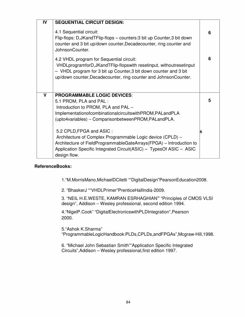
84
IV SEQUENTIAL CIRCUIT DESIGN:
4.1 Sequential circuit:
Flip-flops: D,JKandTFlip-flops – counters:3 bit up Counter,3 bit down
counter and 3 bit up/down counter,Decadecounter, ring counter and
JohnsonCounter.
4.2 VHDL program for Sequential circuit:
VHDLprogramforD,JKandTFlip-flopswith resetinput, withoutresetinput
– VHDL program for 3 bit up Counter,3 bit down counter and 3 bit
up/down counter,Decadecounter, ring counter and JohnsonCounter.
6
6
V PROGRAMMABLE LOGIC DEVICES:
5.1 PROM, PLA and PAL :
Introduction to PROM, PLA and PAL –
ImplementationofcombinationalcircuitswithPROM,PALandPLA
(upto4variables) – ComparisonbetweenPROM,PALandPLA.
5.2 CPLD,FPGA and ASIC :
Architecture of Complex Programmable Logic device (CPLD) –
Architecture of FieldProgrammableGateArrays(FPGA) – Introduction to
Application Specific Integrated Circuit(ASIC) – TypesOf ASIC – ASIC
design flow.
5
6
ReferenceBooks:
1.“M.MorrisMano,MichaelDCiletti ““DigitalDesign”PearsonEducation2008.
2. “BhaskerJ ““VHDLPrimer”PrenticeHallIndia-2009.
3. “NEIL H.E.WESTE, KAMRAN ESRHAGHIAN” “Principles of CMOS VLSI design”, Addison – Wesley professional, second edition 1994.
4.“NigelP.Cook” “DigitalElectronicswithPLDIntegration”,Pearson
2000.
5.“Ashok K.Sharma” “ProgrammableLogicHandbook:PLDs,CPLDs,andFPGAs”,Mcgraw-Hill,1998.
6. “Michael John Sebastian Smith””Application Specific Integrated Circuits”,Addison – Wesley professional,first edition 1997.
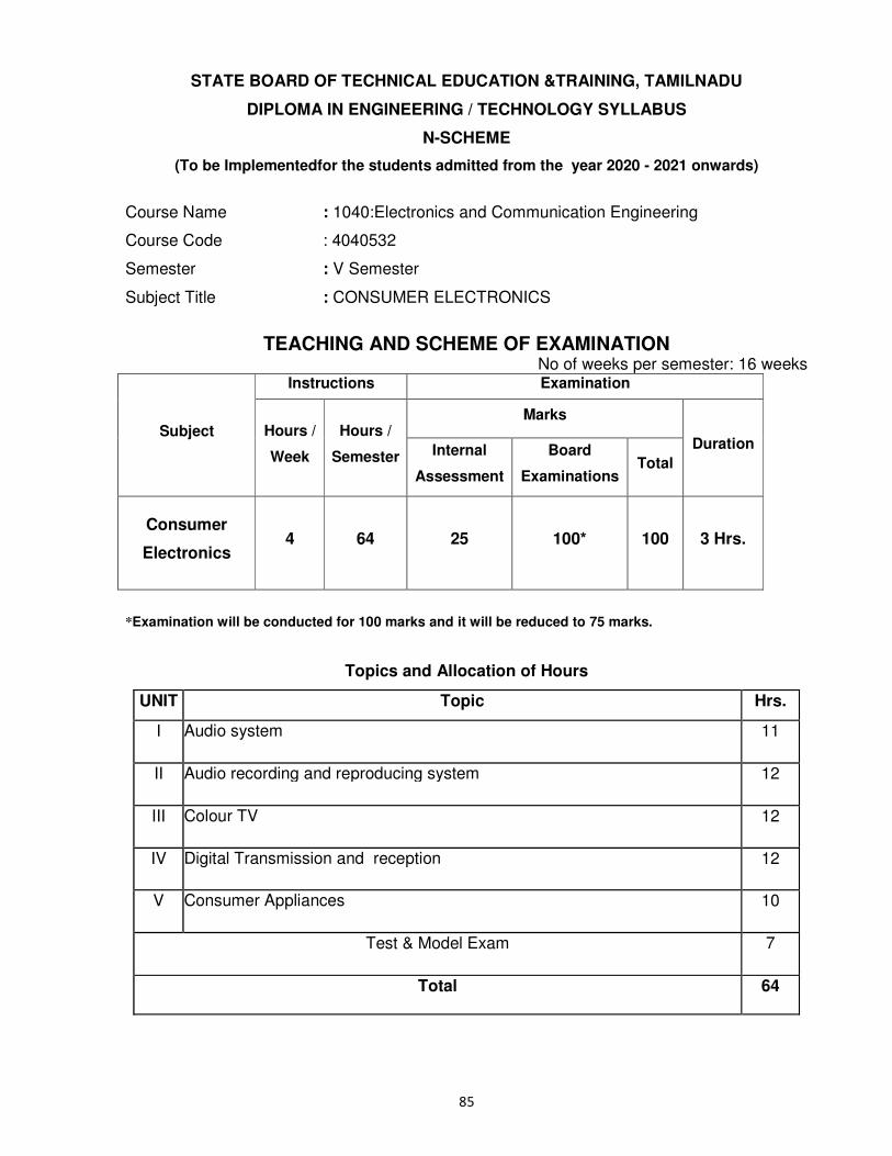
85
STATE BOARD OF TECHNICAL EDUCATION &TRAINING, TAMILNADU
DIPLOMA IN ENGINEERING / TECHNOLOGY SYLLABUS
N-SCHEME
(To be Implementedfor the students admitted from the year 2020 - 2021 onwards)
Course Name : 1040:Electronics and Communication Engineering
Course Code : 4040532
Semester : V Semester
Subject Title : CONSUMER ELECTRONICS
TEACHING AND SCHEME OF EXAMINATION No of weeks per semester: 16 weeks
Subject
Instructions Examination
Hours /
Week
Hours /
Semester
Marks
Duration Internal
Assessment
Board
Examinations Total
Consumer
Electronics 4 64 25 100* 100 3 Hrs.
*Examination will be conducted for 100 marks and it will be reduced to 75 marks.
Topics and Allocation of Hours
UNIT Topic Hrs.
I Audio system 11
II Audio recording and reproducing system 12
III Colour TV 12
IV Digital Transmission and reception 12
V Consumer Appliances 10
Test & Model Exam 7
Total 64
86
RATIONALE:
The objective of teaching this subject is to give students in depth knowledge of various
electronic audio and video devices and systems. Further, this subject will introduce the
students with working principles, block diagram, main features of consumer electronics
Gadgets/goods/devices. This in-turn will develop in them capabilities of assembling, fault
Diagnosis and rectification in a systematic way.
OBJECTIVES:
� Understand the various types of microphones and loud speakers.
� To identify the various digital and analog signal.
� Describe the basis of television and composite video signal.
� Describe the various kinds of colour TV standards and system.
� Compare the various types of digital TV system.
� Understand the various types of consumer goods.
� Maintain various consumer electronic appliances.
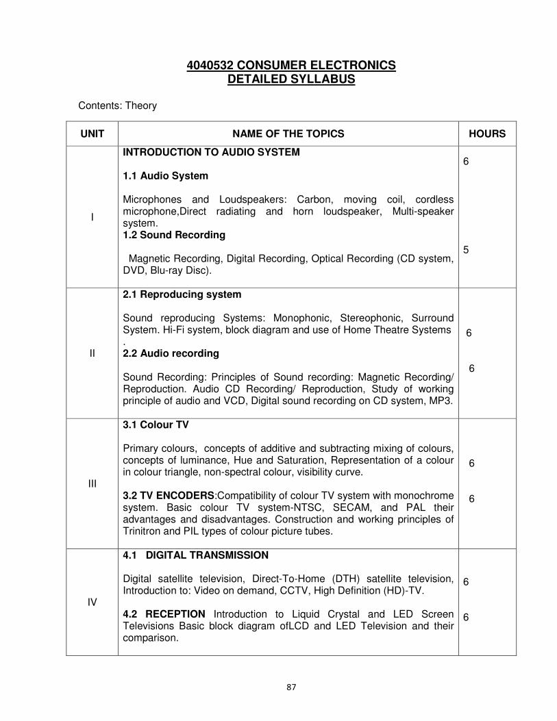
87
4040532 CONSUMER ELECTRONICS
DETAILED SYLLABUS
Contents: Theory
UNIT NAME OF THE TOPICS HOURS
I
INTRODUCTION TO AUDIO SYSTEM 1.1 Audio System Microphones and Loudspeakers: Carbon, moving coil, cordless microphone,Direct radiating and horn loudspeaker, Multi-speaker system. 1.2 Sound Recording Magnetic Recording, Digital Recording, Optical Recording (CD system, DVD, Blu-ray Disc).
6
5
II
2.1 Reproducing system Sound reproducing Systems: Monophonic, Stereophonic, Surround System. Hi-Fi system, block diagram and use of Home Theatre Systems . 2.2 Audio recording Sound Recording: Principles of Sound recording: Magnetic Recording/ Reproduction. Audio CD Recording/ Reproduction, Study of working principle of audio and VCD, Digital sound recording on CD system, MP3.
6
6
III
3.1 Colour TV Primary colours, concepts of additive and subtracting mixing of colours, concepts of luminance, Hue and Saturation, Representation of a colour in colour triangle, non-spectral colour, visibility curve. 3.2 TV ENCODERS:Compatibility of colour TV system with monochrome system. Basic colour TV system-NTSC, SECAM, and PAL their advantages and disadvantages. Construction and working principles of Trinitron and PIL types of colour picture tubes.
6
6
IV
4.1 DIGITAL TRANSMISSION Digital satellite television, Direct-To-Home (DTH) satellite television, Introduction to: Video on demand, CCTV, High Definition (HD)-TV. 4.2 RECEPTION Introduction to Liquid Crystal and LED Screen Televisions Basic block diagram ofLCD and LED Television and their comparison.
6
6
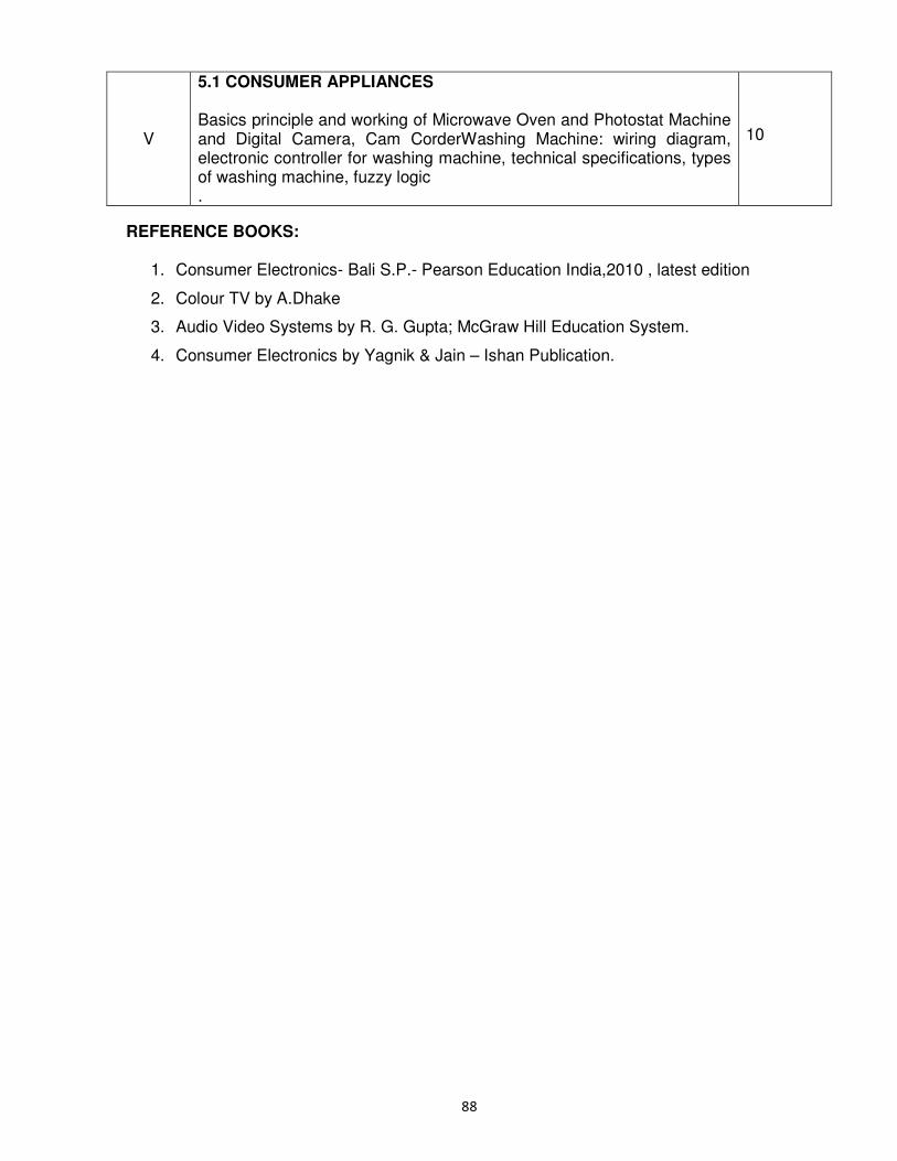
88
REFERENCE BOOKS:
1. Consumer Electronics- Bali S.P.- Pearson Education India,2010 , latest edition
2. Colour TV by A.Dhake
3. Audio Video Systems by R. G. Gupta; McGraw Hill Education System.
4. Consumer Electronics by Yagnik & Jain – Ishan Publication.
V
5.1 CONSUMER APPLIANCES Basics principle and working of Microwave Oven and Photostat Machine and Digital Camera, Cam CorderWashing Machine: wiring diagram, electronic controller for washing machine, technical specifications, types of washing machine, fuzzy logic .
10
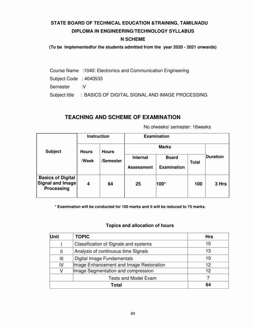
89
STATE BOARD OF TECHNICAL EDUCATION &TRAINING, TAMILNADU
DIPLOMA IN ENGINEERING/TECHNOLOGY SYLLABUS
N SCHEME
(To be Implementedfor the students admitted from the year 2020 - 2021 onwards)
Course Name :1040: Electronics and Communication Engineering
Subject Code : 4040533
Semester :V
Subject title : BASICS OF DIGITAL SIGNAL AND IMAGE PROCESSING
TEACHING AND SCHEME OF EXAMINATION
No ofweeks/ semester: 16weeks
Subject
Instruction Examination
Hours
/Week
Hours
/Semester
Marks Duration Internal
Assessment
Board
Examination
Total
Basics of Digital Signal and Image
Processing
4
64
25
100*
100
3 Hrs
* Examination will be conducted for 100 marks and it will be reduced to 75 marks.
Topics and allocation of hours
Unit TOPIC Hrs
I Classification of Signals and systems 10
II Analysis of continuous time Signals 13
III Digital Image Fundamentals 10
IV Image Enhancement and Image Restoration 12
V Image Segmentation and compression 12
Tests and Model Exam 7
Total 64
90
RATIONALE:
The subject basic of digital signal and image processing introduce
visualization and mathematical representation of continuous time and discrete
time signals and ability to analyses LTI system and give clear explanation of
image compression, restoration, enhancement, segmentation. The student
will have depth of knowledge about signal and image processing which will
help in industries and in bio medical field.
OBJECTIVES:
On completion of the following units of the syllabus contents, the students must be
able to
� Know about basic knowledge of signals and system
� Know fourier representation of periodic signals
� Be able to characterize LTI system
� Steps in image processing
� Simple image fundamental
� Various image enhancement techniques
� Histogram processing
� Spatial filtering
� Understand various compression models
� Study JPEG techniques
� Detection of point, line, edge in images
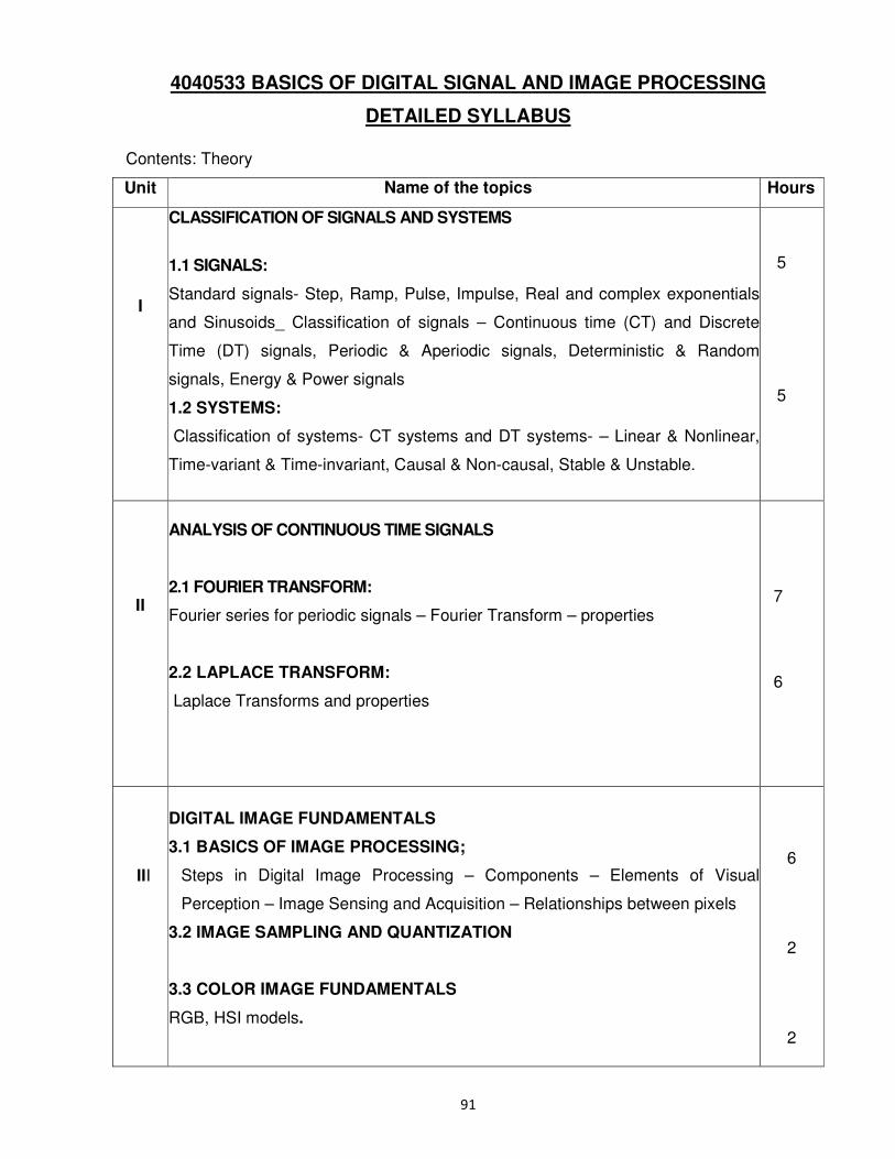
91
4040533 BASICS OF DIGITAL SIGNAL AND IMAGE PROCESSING
DETAILED SYLLABUS
Contents: Theory
Unit Name of the topics Hours
I
CLASSIFICATION OF SIGNALS AND SYSTEMS
1.1 SIGNALS:
Standard signals- Step, Ramp, Pulse, Impulse, Real and complex exponentials
and Sinusoids_ Classification of signals – Continuous time (CT) and Discrete
Time (DT) signals, Periodic & Aperiodic signals, Deterministic & Random
signals, Energy & Power signals
1.2 SYSTEMS:
Classification of systems- CT systems and DT systems- – Linear & Nonlinear,
Time-variant & Time-invariant, Causal & Non-causal, Stable & Unstable.
5 5
II
ANALYSIS OF CONTINUOUS TIME SIGNALS
2.1 FOURIER TRANSFORM:
Fourier series for periodic signals – Fourier Transform – properties
2.2 LAPLACE TRANSFORM:
Laplace Transforms and properties
7
6
III
DIGITAL IMAGE FUNDAMENTALS
3.1 BASICS OF IMAGE PROCESSING;
Steps in Digital Image Processing – Components – Elements of Visual
Perception – Image Sensing and Acquisition – Relationships between pixels
3.2 IMAGE SAMPLING AND QUANTIZATION
3.3 COLOR IMAGE FUNDAMENTALS
RGB, HSI models.
6
2
2
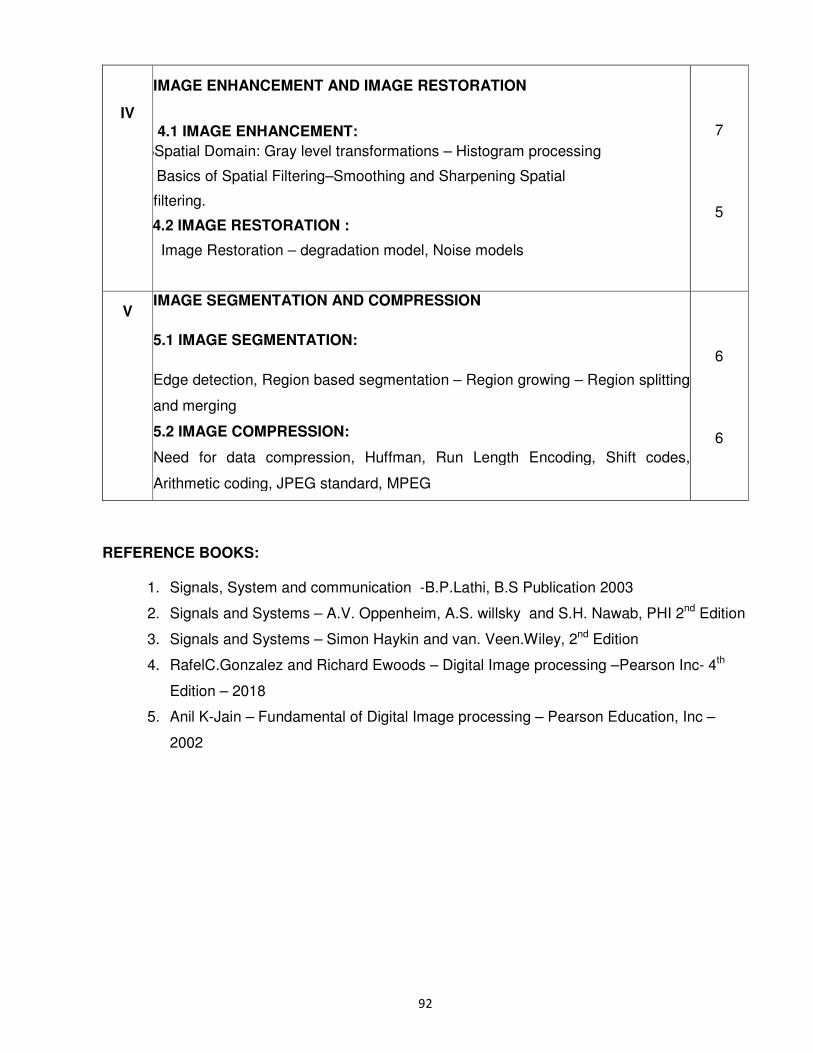
92
IV
IMAGE ENHANCEMENT AND IMAGE RESTORATION
4.1 IMAGE ENHANCEMENT:
SSpatial Domain: Gray level transformations – Histogram processing
Basics of Spatial Filtering–Smoothing and Sharpening Spatial
Ffiltering.
4.2 IMAGE RESTORATION :
II Image Restoration – degradation model, Noise models
7
5
V
IMAGE SEGMENTATION AND COMPRESSION
5.1 IMAGE SEGMENTATION:
Edge detection, Region based segmentation – Region growing – Region splitting
and merging
5.2 IMAGE COMPRESSION:
Need for data compression, Huffman, Run Length Encoding, Shift codes,
Arithmetic coding, JPEG standard, MPEG
6
6
REFERENCE BOOKS:
1. Signals, System and communication -B.P.Lathi, B.S Publication 2003
2. Signals and Systems – A.V. Oppenheim, A.S. willsky and S.H. Nawab, PHI 2nd Edition
3. Signals and Systems – Simon Haykin and van. Veen.Wiley, 2nd Edition
4. RafelC.Gonzalez and Richard Ewoods – Digital Image processing –Pearson Inc- 4th
Edition – 2018
5. Anil K-Jain – Fundamental of Digital Image processing – Pearson Education, Inc –
2002
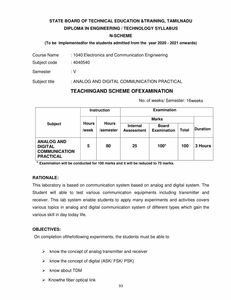
93
STATE BOARD OF TECHNICAL EDUCATION &TRAINING, TAMILNADU
DIPLOMA IN ENGINEERING / TECHNOLOGY SYLLABUS
N-SCHEME
(To be Implementedfor the students admitted from the year 2020 - 2021 onwards)
Course Name : 1040:Electronics and Communication Engineering
Subject code : 4040540 Semester : V Subject title : ANALOG AND DIGITAL COMMUNICATION PRACTICAL
TEACHINGAND SCHEME OFEXAMINATION
No. of weeks/ Semester: 16weeks
Subject
Instruction Examination
Hours
/week
Hours
/semester
Marks Duration
Internal Assessment
Board Examination
Total
ANALOG AND DIGITAL COMMUNICATION PRACTICAL
5
80
25
100*
100
3 Hours
* Examination will be conducted for 100 marks and it will be reduced to 75 marks.
RATIONALE:
This laboratory is based on communication system based on analog and digital system. The
Student will able to test various communication equipments including transmitter and
receiver. This lab system enable students to apply many experiments and activities covers
various topics in analog and digital communication system of different types which gain the
various skill in day today life.
OBJECTIVES:
On completion ofthefollowing experiments, the students must be able to
� know the concept of analog transmitter and receiver
� know the concept of digital (ASK/ FSK/ PSK)
� know about TDM
� Knowthe fiber optical link
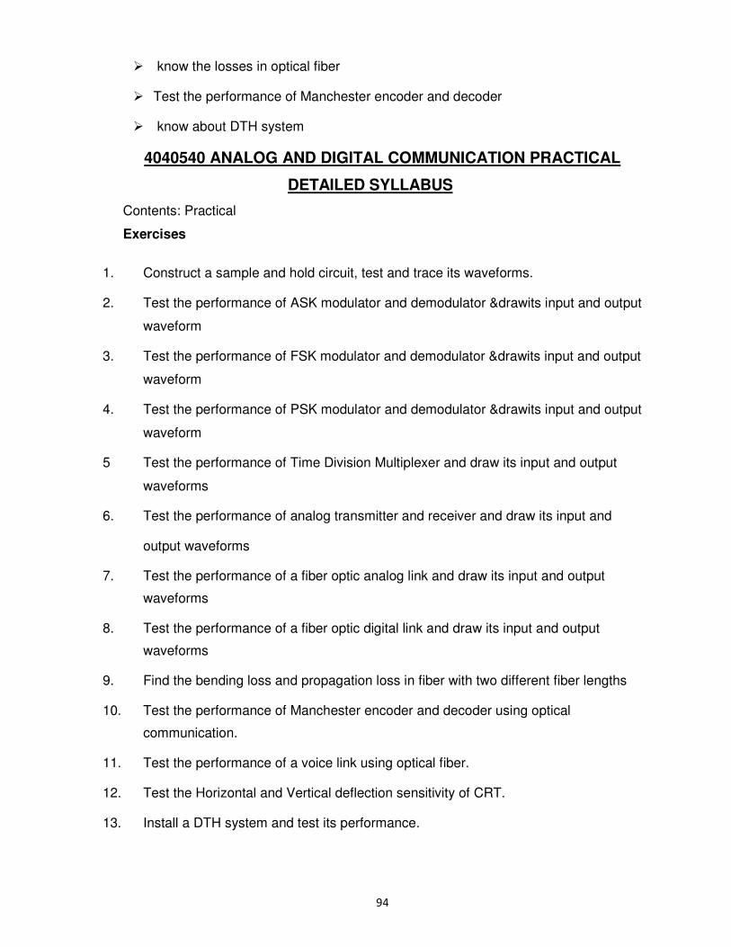
94
� know the losses in optical fiber
� Test the performance of Manchester encoder and decoder
� know about DTH system
4040540 ANALOG AND DIGITAL COMMUNICATION PRACTICAL
DETAILED SYLLABUS
Contents: Practical
Exercises
1. Construct a sample and hold circuit, test and trace its waveforms.
2. Test the performance of ASK modulator and demodulator &drawits input and output
waveform
3. Test the performance of FSK modulator and demodulator &drawits input and output
waveform
4. Test the performance of PSK modulator and demodulator &drawits input and output
waveform
5 Test the performance of Time Division Multiplexer and draw its input and output
waveforms
6. Test the performance of analog transmitter and receiver and draw its input and
output waveforms
7. Test the performance of a fiber optic analog link and draw its input and output
waveforms
8. Test the performance of a fiber optic digital link and draw its input and output
waveforms
9. Find the bending loss and propagation loss in fiber with two different fiber lengths
10. Test the performance of Manchester encoder and decoder using optical
communication.
11. Test the performance of a voice link using optical fiber.
12. Test the Horizontal and Vertical deflection sensitivity of CRT.
13. Install a DTH system and test its performance.
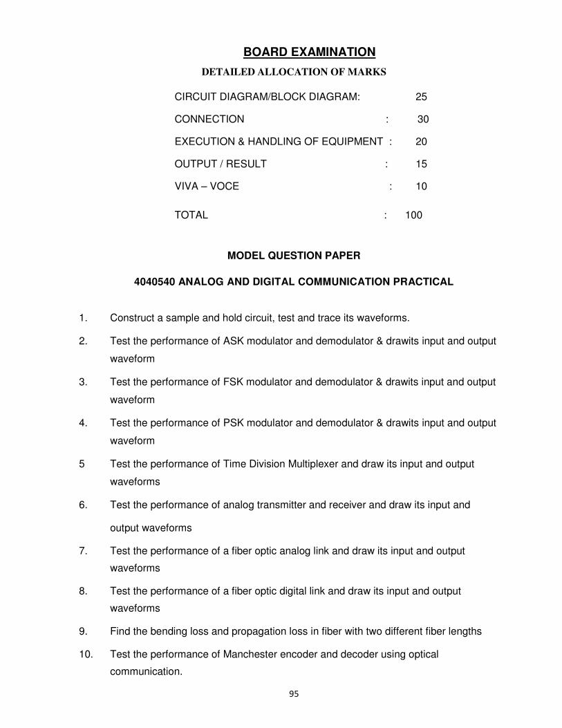
95
BOARD EXAMINATION
DETAILED ALLOCATION OF MARKS
MODEL QUESTION PAPER
4040540 ANALOG AND DIGITAL COMMUNICATION PRACTICAL
1. Construct a sample and hold circuit, test and trace its waveforms.
2. Test the performance of ASK modulator and demodulator & drawits input and output
waveform
3. Test the performance of FSK modulator and demodulator & drawits input and output
waveform
4. Test the performance of PSK modulator and demodulator & drawits input and output
waveform
5 Test the performance of Time Division Multiplexer and draw its input and output
waveforms
6. Test the performance of analog transmitter and receiver and draw its input and
output waveforms
7. Test the performance of a fiber optic analog link and draw its input and output
waveforms
8. Test the performance of a fiber optic digital link and draw its input and output
waveforms
9. Find the bending loss and propagation loss in fiber with two different fiber lengths
10. Test the performance of Manchester encoder and decoder using optical
communication.
CIRCUIT DIAGRAM/BLOCK DIAGRAM: 25 CONNECTION :
30
EXECUTION & HANDLING OF EQUIPMENT :
20
OUTPUT / RESULT :
15
VIVA – VOCE :
10
TOTAL : 100
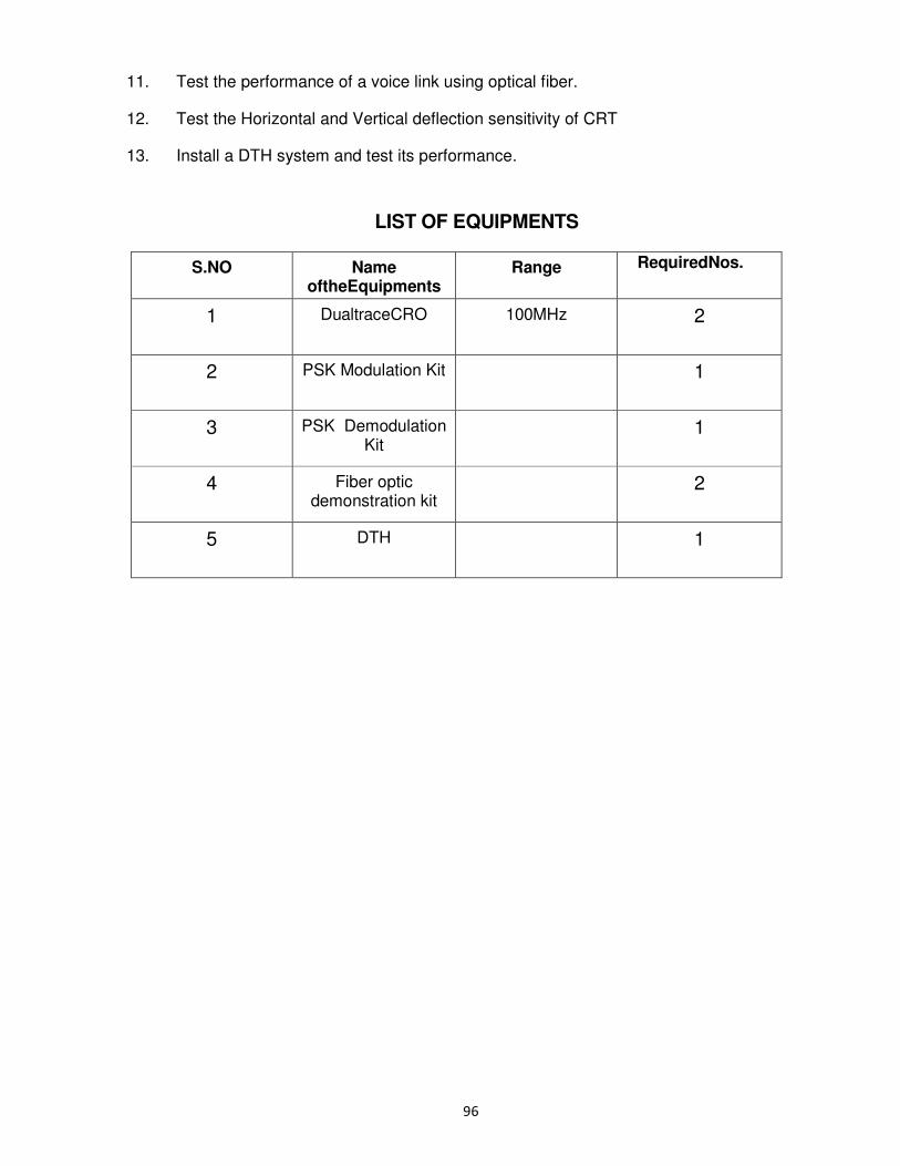
96
11. Test the performance of a voice link using optical fiber.
12. Test the Horizontal and Vertical deflection sensitivity of CRT
13. Install a DTH system and test its performance.
LIST OF EQUIPMENTS
S.NO Name oftheEquipments
Range RequiredNos.
1 DualtraceCRO 100MHz 2
2 PSK Modulation Kit 1
3 PSK Demodulation Kit
1
4 Fiber optic demonstration kit
2
5
DTH 1
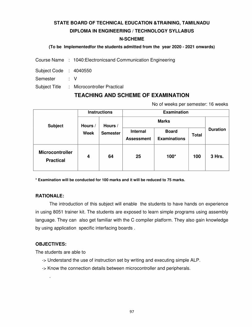
97
STATE BOARD OF TECHNICAL EDUCATION &TRAINING, TAMILNADU
DIPLOMA IN ENGINEERING / TECHNOLOGY SYLLABUS
N-SCHEME
(To be Implementedfor the students admitted from the year 2020 - 2021 onwards)
Course Name : 1040:Electronicsand Communication Engineering Subject Code : 4040550
Semester : V
Subject Title : Microcontroller Practical
TEACHING AND SCHEME OF EXAMINATION
No of weeks per semester: 16 weeks
Subject
Instructions Examination
Hours /
Week
Hours /
Semester
Marks
Duration Internal
Assessment
Board
Examinations Total
Microcontroller
Practical 4 64 25 100* 100 3 Hrs.
* Examination will be conducted for 100 marks and it will be reduced to 75 marks.
RATIONALE:
The introduction of this subject will enable the students to have hands on experience
in using 8051 trainer kit. The students are exposed to learn simple programs using assembly
language. They can also get familiar with the C compiler platform. They also gain knowledge
by using application specific interfacing boards .
OBJECTIVES:
The students are able to
-> Understand the use of instruction set by writing and executing simple ALP.
-> Know the connection details between microcontroller and peripherals.
.
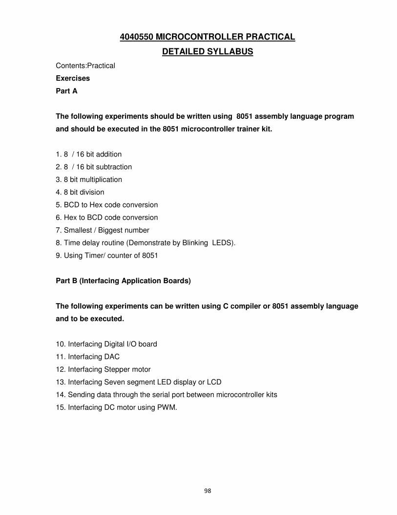
98
4040550 MICROCONTROLLER PRACTICAL
DETAILED SYLLABUS
Contents:Practical
Exercises
Part A
The following experiments should be written using 8051 assembly language program
and should be executed in the 8051 microcontroller trainer kit.
1. 8 / 16 bit addition
2. 8 / 16 bit subtraction
3. 8 bit multiplication
4. 8 bit division
5. BCD to Hex code conversion
6. Hex to BCD code conversion
7. Smallest / Biggest number
8. Time delay routine (Demonstrate by Blinking LEDS).
9. Using Timer/ counter of 8051
Part B (Interfacing Application Boards)
The following experiments can be written using C compiler or 8051 assembly language
and to be executed.
10. Interfacing Digital I/O board
11. Interfacing DAC
12. Interfacing Stepper motor
13. Interfacing Seven segment LED display or LCD
14. Sending data through the serial port between microcontroller kits
15. Interfacing DC motor using PWM.
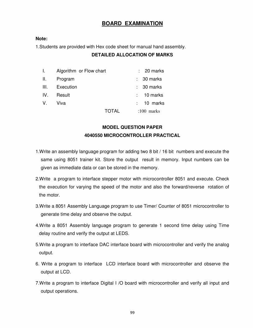
99
BOARD EXAMINATION
Note:
1.Students are provided with Hex code sheet for manual hand assembly.
DETAILED ALLOCATION OF MARKS
I. Algorithm or Flow chart : 20 marks
II. Program : 30 marks
III. Execution : 30 marks
IV. Result : 10 marks
V. Viva : 10 marks
TOTAL :100 marks
MODEL QUESTION PAPER
4040550 MICROCONTROLLER PRACTICAL
1.Write an assembly language program for adding two 8 bit / 16 bit numbers and execute the
same using 8051 trainer kit. Store the output result in memory. Input numbers can be
given as immediate data or can be stored in the memory.
2.Write a program to interface stepper motor with microcontroller 8051 and execute. Check
the execution for varying the speed of the motor and also the forward/reverse rotation of
the motor.
3.Write a 8051 Assembly Language program to use Timer/ Counter of 8051 microcontroller to
generate time delay and observe the output.
4.Write a 8051 Assembly language program to generate 1 second time delay using Time
delay routine and verify the output at LEDS.
5.Write a program to interface DAC interface board with microcontroller and verify the analog
output.
6. Write a program to interface LCD interface board with microcontroller and observe the
output at LCD.
7.Write a program to interface Digital I /O board with microcontroller and verify all input and
output operations.
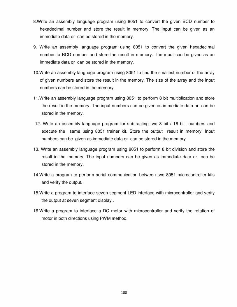
100
8.Write an assembly language program using 8051 to convert the given BCD number to
hexadecimal number and store the result in memory. The input can be given as an
immediate data or can be stored in the memory.
9. Write an assembly language program using 8051 to convert the given hexadecimal
number to BCD number and store the result in memory. The input can be given as an
immediate data or can be stored in the memory.
10.Write an assembly language program using 8051 to find the smallest number of the array
of given numbers and store the result in the memory. The size of the array and the input
numbers can be stored in the memory.
11.Write an assembly language program using 8051 to perform 8 bit multiplication and store
the result in the memory. The input numbers can be given as immediate data or can be
stored in the memory.
12. Write an assembly language program for subtracting two 8 bit / 16 bit numbers and
execute the same using 8051 trainer kit. Store the output result in memory. Input
numbers can be given as immediate data or can be stored in the memory.
13. Write an assembly language program using 8051 to perform 8 bit division and store the
result in the memory. The input numbers can be given as immediate data or can be
stored in the memory.
14.Write a program to perform serial communication between two 8051 microcontroller kits
and verify the output.
15.Write a program to interface seven segment LED interface with microcontroller and verify
the output at seven segment display .
16.Write a program to interface a DC motor with microcontroller and verify the rotation of
motor in both directions using PWM method.
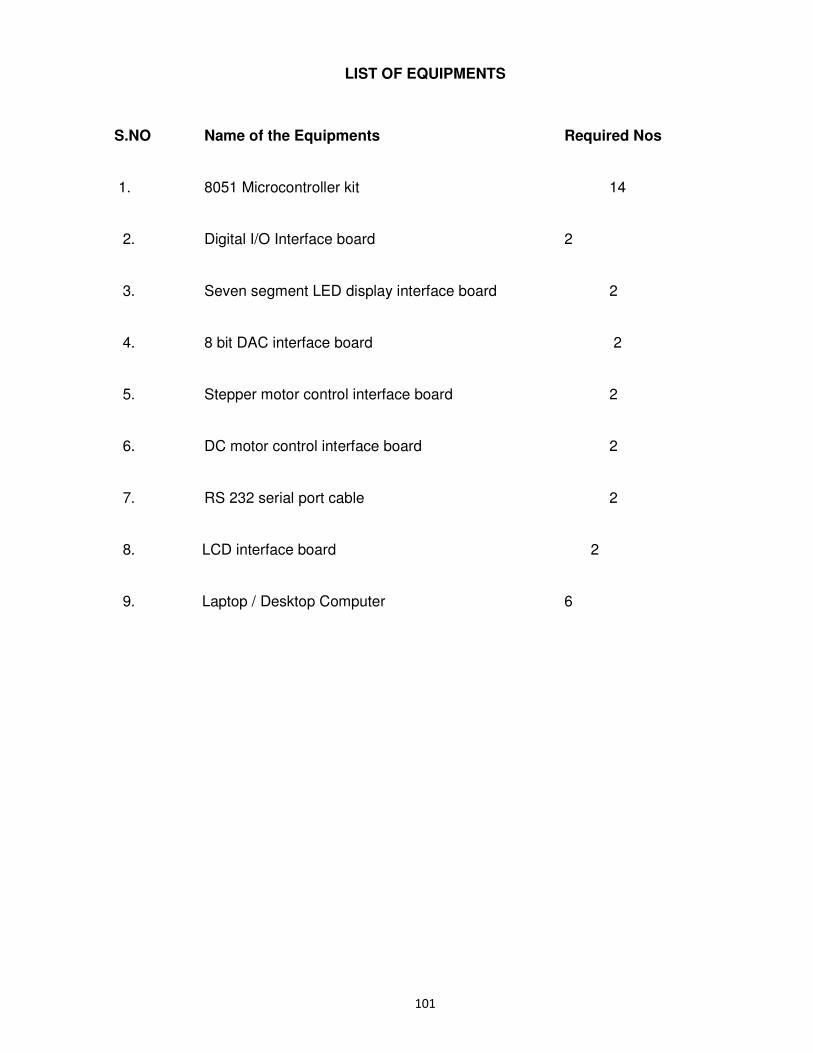
101
LIST OF EQUIPMENTS
S.NO Name of the Equipments Required Nos
1. 8051 Microcontroller kit 14
2. Digital I/O Interface board 2
3. Seven segment LED display interface board 2
4. 8 bit DAC interface board 2
5. Stepper motor control interface board 2
6. DC motor control interface board 2
7. RS 232 serial port cable 2
8. LCD interface board 2
9. Laptop / Desktop Computer 6
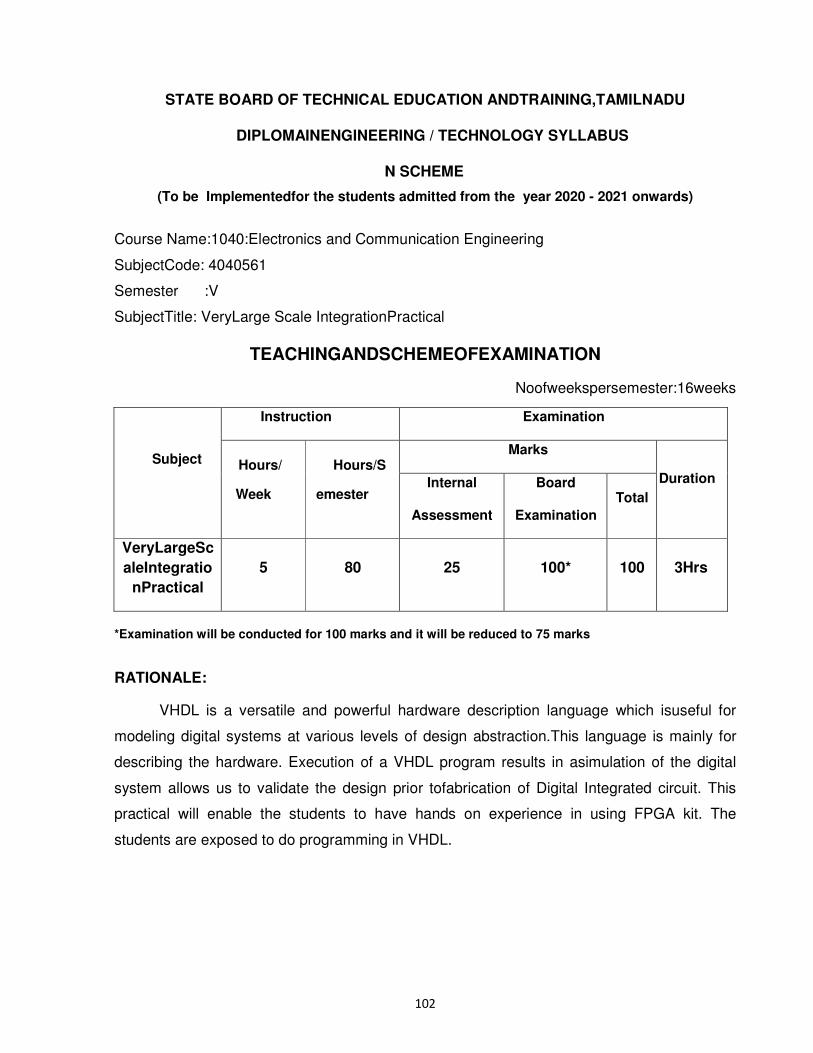
102
STATE BOARD OF TECHNICAL EDUCATION ANDTRAINING,TAMILNADU
DIPLOMAINENGINEERING / TECHNOLOGY SYLLABUS
N SCHEME
(To be Implementedfor the students admitted from the year 2020 - 2021 onwards)
Course Name:1040:Electronics and Communication Engineering
SubjectCode: 4040561
Semester :V
SubjectTitle: VeryLarge Scale IntegrationPractical
TEACHINGANDSCHEMEOFEXAMINATION
Noofweekspersemester:16weeks
*Examination will be conducted for 100 marks and it will be reduced to 75 marks
RATIONALE:
VHDL is a versatile and powerful hardware description language which isuseful for
modeling digital systems at various levels of design abstraction.This language is mainly for
describing the hardware. Execution of a VHDL program results in asimulation of the digital
system allows us to validate the design prior tofabrication of Digital Integrated circuit. This
practical will enable the students to have hands on experience in using FPGA kit. The
students are exposed to do programming in VHDL.
Subject
Instruction Examination
Hours/
Week
Hours/S
emester
Marks
Duration Internal
Assessment
Board
Examination
Total
VeryLargeSc
aleIntegratio
nPractical
5
80
25
100*
100
3Hrs
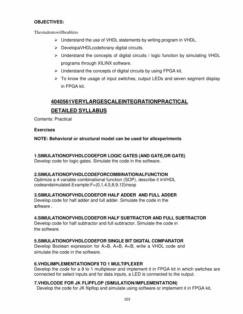
103
OBJECTIVES: Thestudentswillbeableto
� Understand the use of VHDL statements by writing program in VHDL.
� DevelopaVHDLcodeforany digital circuits.
� Understand the concepts of digital circuits / logic function by simulating VHDL
programs through XILINX software.
� Understand the concepts of digital circuits by using FPGA kit.
� To know the usage of input switches, output LEDs and seven segment display
in FPGA kit.
4040561VERYLARGESCALEINTEGRATIONPRACTICAL
DETAILED SYLLABUS
Contents: Practical
Exercises
NOTE: Behavioral or structural model can be used for allexperiments
1.SIMULATIONOFVHDLCODEFOR LOGIC GATES (AND GATE,OR GATE) Develop code for logic gates. Simulate the code in the software.
2.SIMULATIONOFVHDLCODEFORCOMBINATIONALFUNCTION Optimize a 4 variable combinational function (SOP), describe it inVHDL codeandsimulateit.Example:F=(0,1,4,5,8,9,12)insop 3.SIMULATIONOFVHDLCODEFOR HALF ADDER AND FULL ADDER Develop code for half adder and full adder. Simulate the code in the
software .
4.SIMULATIONOFVHDLCODEFOR HALF SUBTRACTOR AND FULL SUBTRACTOR Develop code for half subtractor and full subtractor. Simulate the code in
the software.
5.SIMULATIONOFVHDLCODEFOR SINGLE BIT DIGITAL COMPARATOR Develop Boolean expression for A>B, A=B, A<B, write a VHDL code and
simulate the code in the software.
6.VHDLIMPLEMENTATIONOF8 TO 1 MULTIPLEXER Develop the code for a 8 to 1 multiplexer and implement it in FPGA kit in which switches are connected for select inputs and for data inputs, a LED is connected to the output.
7.VHDLCODE FOR JK FLIPFLOP (SIMULATION/IMPLEMENTATION) Develop the code for JK flipflop and simulate using software or implement it in FPGA kit.
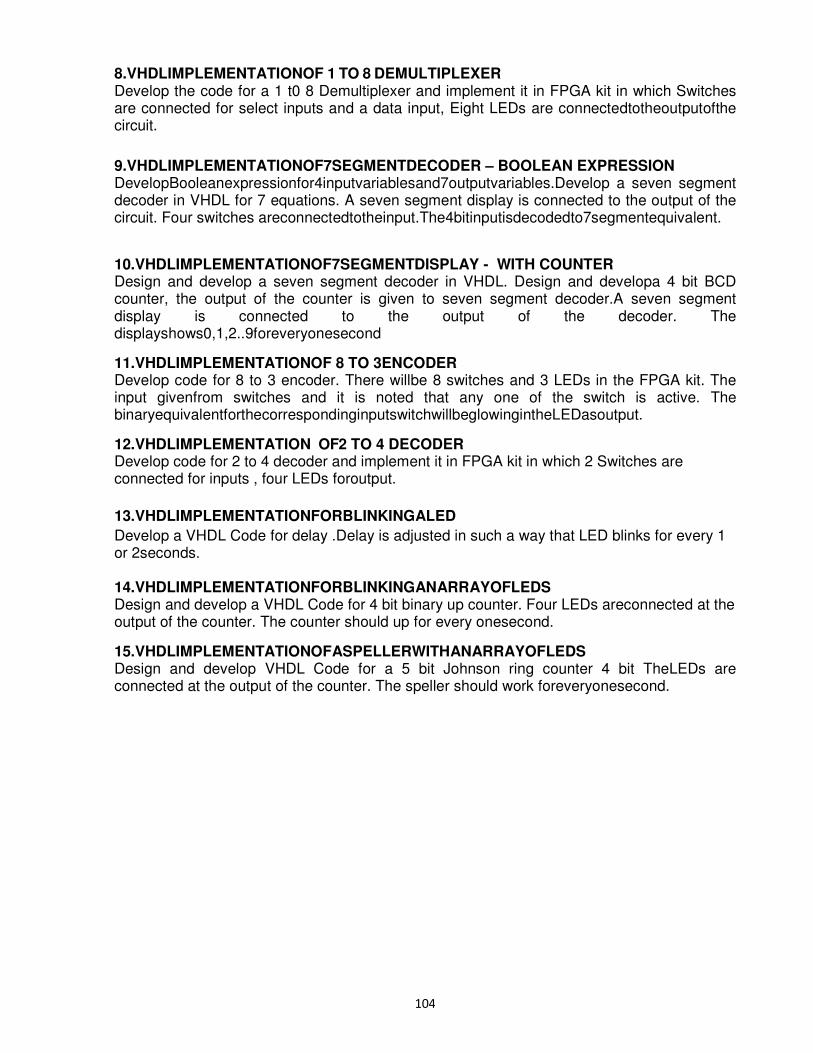
104
8.VHDLIMPLEMENTATIONOF 1 TO 8 DEMULTIPLEXER Develop the code for a 1 t0 8 Demultiplexer and implement it in FPGA kit in which Switches are connected for select inputs and a data input, Eight LEDs are connectedtotheoutputofthe circuit.
9.VHDLIMPLEMENTATIONOF7SEGMENTDECODER – BOOLEAN EXPRESSION DevelopBooleanexpressionfor4inputvariablesand7outputvariables.Develop a seven segment decoder in VHDL for 7 equations. A seven segment display is connected to the output of the circuit. Four switches areconnectedtotheinput.The4bitinputisdecodedto7segmentequivalent.
10.VHDLIMPLEMENTATIONOF7SEGMENTDISPLAY - WITH COUNTER Design and develop a seven segment decoder in VHDL. Design and developa 4 bit BCD counter, the output of the counter is given to seven segment decoder.A seven segment display is connected to the output of the decoder. The displayshows0,1,2..9foreveryonesecond
11.VHDLIMPLEMENTATIONOF 8 TO 3ENCODER Develop code for 8 to 3 encoder. There willbe 8 switches and 3 LEDs in the FPGA kit. The input givenfrom switches and it is noted that any one of the switch is active. The binaryequivalentforthecorrespondinginputswitchwillbeglowingintheLEDasoutput.
12.VHDLIMPLEMENTATION OF2 TO 4 DECODER Develop code for 2 to 4 decoder and implement it in FPGA kit in which 2 Switches are connected for inputs , four LEDs foroutput.
13.VHDLIMPLEMENTATIONFORBLINKINGALED
Develop a VHDL Code for delay .Delay is adjusted in such a way that LED blinks for every 1 or 2seconds. 14.VHDLIMPLEMENTATIONFORBLINKINGANARRAYOFLEDS Design and develop a VHDL Code for 4 bit binary up counter. Four LEDs areconnected at the output of the counter. The counter should up for every onesecond.
15.VHDLIMPLEMENTATIONOFASPELLERWITHANARRAYOFLEDS Design and develop VHDL Code for a 5 bit Johnson ring counter 4 bit TheLEDs are connected at the output of the counter. The speller should work foreveryonesecond.
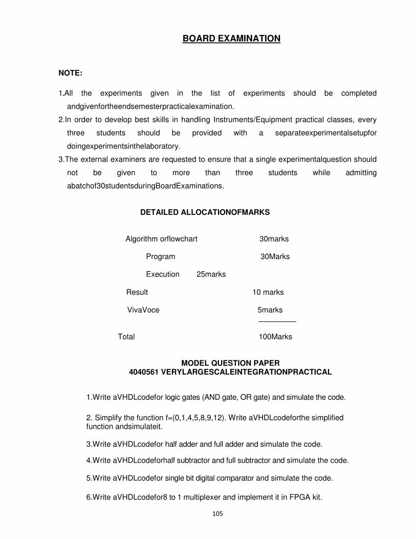
105
BOARD EXAMINATION
NOTE:
1.All the experiments given in the list of experiments should be completed
andgivenfortheendsemesterpracticalexamination.
2.In order to develop best skills in handling Instruments/Equipment practical classes, every
three students should be provided with a separateexperimentalsetupfor
doingexperimentsinthelaboratory.
3.The external examiners are requested to ensure that a single experimentalquestion should
not be given to more than three students while admitting
abatchof30studentsduringBoardExaminations.
DETAILED ALLOCATIONOFMARKS
Algorithm orflowchart 30marks
Program 30Marks
Execution 25marks
Result 10 marks
VivaVoce 5marks
Total 100Marks
MODEL QUESTION PAPER
4040561 VERYLARGESCALEINTEGRATIONPRACTICAL
1.Write aVHDLcodefor logic gates (AND gate, OR gate) and simulate the code.
2. Simplify the function f=(0,1,4,5,8,9,12). Write aVHDLcodeforthe simplified function andsimulateit.
3.Write aVHDLcodefor half adder and full adder and simulate the code.
4.Write aVHDLcodeforhalf subtractor and full subtractor and simulate the code.
5.Write aVHDLcodefor single bit digital comparator and simulate the code.
6.Write aVHDLcodefor8 to 1 multiplexer and implement it in FPGA kit.
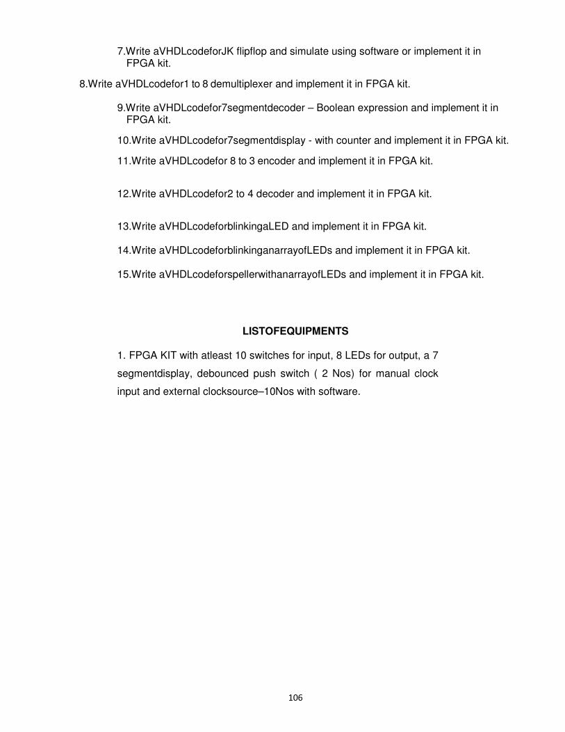
106
7.Write aVHDLcodeforJK flipflop and simulate using software or implement it in FPGA kit.
8.Write aVHDLcodefor1 to 8 demultiplexer and implement it in FPGA kit.
9.Write aVHDLcodefor7segmentdecoder – Boolean expression and implement it in FPGA kit.
10.Write aVHDLcodefor7segmentdisplay - with counter and implement it in FPGA kit.
11.Write aVHDLcodefor 8 to 3 encoder and implement it in FPGA kit.
12.Write aVHDLcodefor2 to 4 decoder and implement it in FPGA kit.
13.Write aVHDLcodeforblinkingaLED and implement it in FPGA kit.
14.Write aVHDLcodeforblinkinganarrayofLEDs and implement it in FPGA kit.
15.Write aVHDLcodeforspellerwithanarrayofLEDs and implement it in FPGA kit.
LISTOFEQUIPMENTS
1. FPGA KIT with atleast 10 switches for input, 8 LEDs for output, a 7
segmentdisplay, debounced push switch ( 2 Nos) for manual clock
input and external clocksource–10Nos with software.
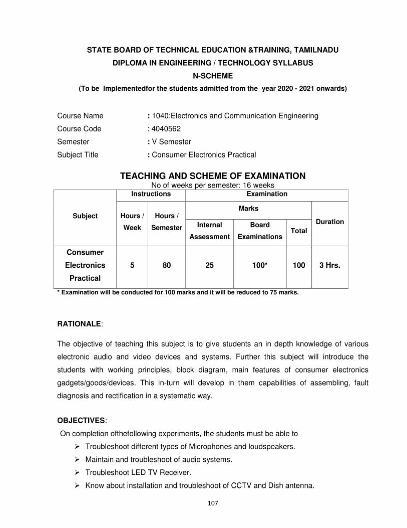
107
STATE BOARD OF TECHNICAL EDUCATION &TRAINING, TAMILNADU
DIPLOMA IN ENGINEERING / TECHNOLOGY SYLLABUS
N-SCHEME
(To be Implementedfor the students admitted from the year 2020 - 2021 onwards)
Course Name : 1040:Electronics and Communication Engineering
Course Code : 4040562
Semester : V Semester
Subject Title : Consumer Electronics Practical
TEACHING AND SCHEME OF EXAMINATION No of weeks per semester: 16 weeks
Subject
Instructions Examination
Hours /
Week
Hours /
Semester
Marks
Duration Internal
Assessment
Board
Examinations Total
Consumer
Electronics
Practical
5 80 25 100* 100 3 Hrs.
* Examination will be conducted for 100 marks and it will be reduced to 75 marks.
RATIONALE:
The objective of teaching this subject is to give students an in depth knowledge of various
electronic audio and video devices and systems. Further this subject will introduce the
students with working principles, block diagram, main features of consumer electronics
gadgets/goods/devices. This in-turn will develop in them capabilities of assembling, fault
diagnosis and rectification in a systematic way.
OBJECTIVES:
On completion ofthefollowing experiments, the students must be able to
� Troubleshoot different types of Microphones and loudspeakers.
� Maintain and troubleshoot of audio systems.
� Troubleshoot LED TV Receiver.
� Know about installation and troubleshoot of CCTV and Dish antenna.
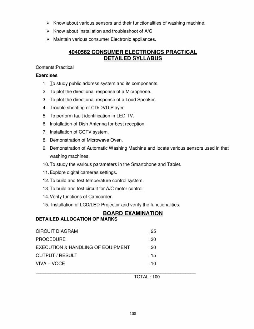
108
� Know about various sensors and their functionalities of washing machine.
� Know about Installation and troubleshoot of A/C
� Maintain various consumer Electronic appliances.
4040562 CONSUMER ELECTRONICS PRACTICAL DETAILED SYLLABUS
Contents:Practical
Exercises
1. To study public address system and its components.
2. To plot the directional response of a Microphone.
3. To plot the directional response of a Loud Speaker.
4. Trouble shooting of CD/DVD Player.
5. To perform fault identification in LED TV.
6. Installation of Dish Antenna for best reception.
7. Installation of CCTV system.
8. Demonstration of Microwave Oven.
9. Demonstration of Automatic Washing Machine and locate various sensors used in that
washing machines.
10. To study the various parameters in the Smartphone and Tablet.
11. Explore digital cameras settings.
12. To build and test temperature control system.
13. To build and test circuit for A/C motor control.
14. Verify functions of Camcorder.
15. Installation of LCD/LED Projector and verify the functionalities.
BOARD EXAMINATION DETAILED ALLOCATION OF MARKS
CIRCUIT DIAGRAM : 25
PROCEDURE : 30
EXECUTION & HANDLING OF EQUIPMENT : 20
OUTPUT / RESULT : 15
VIVA – VOCE : 10
________________________________________________________________ TOTAL : 100
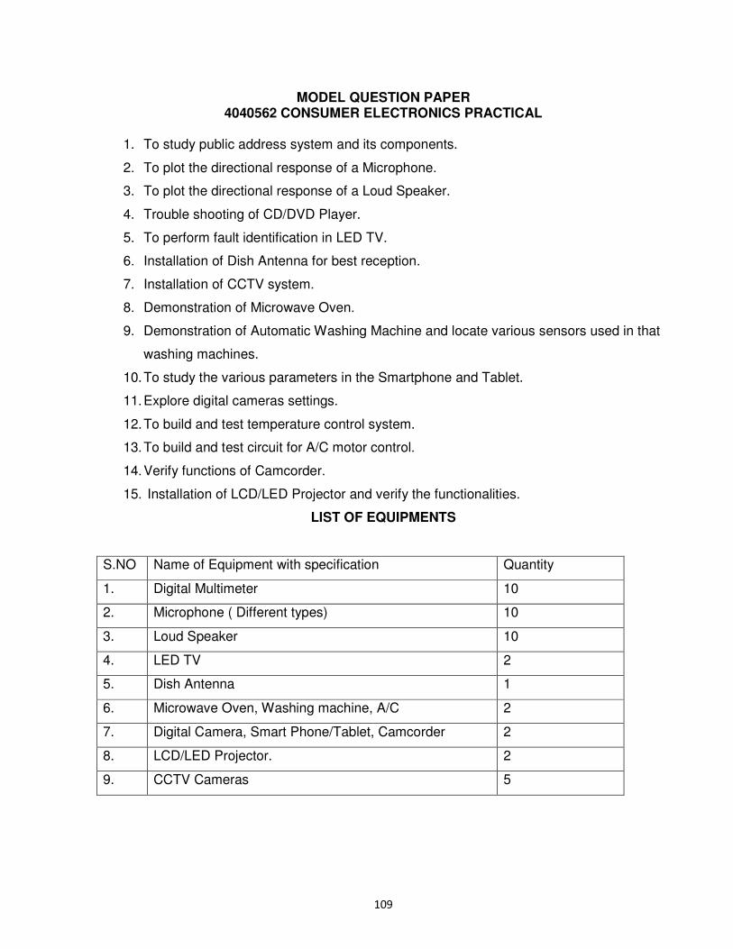
109
MODEL QUESTION PAPER 4040562 CONSUMER ELECTRONICS PRACTICAL
1. To study public address system and its components.
2. To plot the directional response of a Microphone.
3. To plot the directional response of a Loud Speaker.
4. Trouble shooting of CD/DVD Player.
5. To perform fault identification in LED TV.
6. Installation of Dish Antenna for best reception.
7. Installation of CCTV system.
8. Demonstration of Microwave Oven.
9. Demonstration of Automatic Washing Machine and locate various sensors used in that
washing machines.
10. To study the various parameters in the Smartphone and Tablet.
11. Explore digital cameras settings.
12. To build and test temperature control system.
13. To build and test circuit for A/C motor control.
14. Verify functions of Camcorder.
15. Installation of LCD/LED Projector and verify the functionalities.
LIST OF EQUIPMENTS
S.NO Name of Equipment with specification Quantity
1. Digital Multimeter 10
2. Microphone ( Different types) 10
3. Loud Speaker 10
4. LED TV 2
5. Dish Antenna 1
6. Microwave Oven, Washing machine, A/C 2
7. Digital Camera, Smart Phone/Tablet, Camcorder 2
8. LCD/LED Projector. 2
9. CCTV Cameras 5
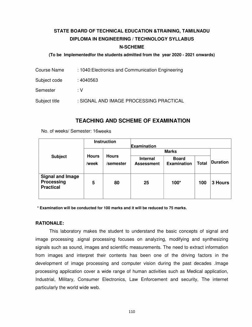
110
STATE BOARD OF TECHNICAL EDUCATION &TRAINING, TAMILNADU
DIPLOMA IN ENGINEERING / TECHNOLOGY SYLLABUS
N-SCHEME
(To be Implementedfor the students admitted from the year 2020 - 2021 onwards)
Course Name : 1040:Electronics and Communication Engineering
Subject code : 4040563 Semester : V Subject title : SIGNAL AND IMAGE PROCESSING PRACTICAL
TEACHING AND SCHEME OF EXAMINATION
No. of weeks/ Semester: 16weeks
Subject
Instruction Examination
Hours
/week
Hours
/semester
Marks Duration
Internal Assessment
Board Examination
Total
Signal and Image Processing Practical
5
80
25
100*
100
3 Hours
* Examination will be conducted for 100 marks and it will be reduced to 75 marks.
RATIONALE:
This laboratory makes the student to understand the basic concepts of signal and
image processing .signal processing focuses on analyzing, modifying and synthesizing
signals such as sound, images and scientific measurements. The need to extract information
from images and interpret their contents has been one of the driving factors in the
development of image processing and computer vision during the past decades .Image
processing application cover a wide range of human activities such as Medical application,
Industrial, Military, Consumer Electronics, Law Enforcement and security, The internet
particularly the world wide web.
111
OBJECTIVES:
On completion ofthefollowing experiments, the students must be able to
� know to generate discrete sequence signal.
� knowabout fourier transform
� know first order low pass filter and first order high pass filter
� know about spatial domain
� know about contrast stretching.
� know graylevel slicing and bitplane slicing
� know about masking
� know frequency domain of ideal lowpass filter and ideal high pass filter
4040563 SIGNAL AND IMAGE PROCESSING PRACTICAL
DETAILED SYLLABUS
Contents: Practical Exercises
1. Write a MATLAB program to generate the discrete sequence unit step and unit
impulse. Plot all sequences
2. Write a MATLAB program to generate the discrete sequence ramp and periodic
sinusoidal signal.plot all sequences.
3. Find the Fourier transform of a square pulse using MATLAB .Plot its amplitude and
phase spectrum.
4. Write a MATLAB program to generate a random sinusoidal signal and plot four
possible realizations of random signals
5. Write a MATLAB program to find the magnitude and phase response of first order low
pass filter. Plot the responses in logarithmic scale.
6. Write a MATLAB program to find the magnitude and phase response of first order high
pass filter. Plot the responses in logarithmic scale.
7. Write a MATLAB program in spatial domain for image negatives and log transformation
8. Obtain the power law transformation in spatial domain using MATLAB.
9. Write a MATLAB program for contrast stretching.
10. Write a MATLAB program in spatial domain for linear filter
11. Write a MATLAB program for graylevel slicing andbitplane slicing.
12. Write a MATLAB program for histogram equalization
112
13. Write a MATLAB program for unsharp masking.
14. Obtain the frequency domain of ideal lowpass filter in MATLAB.
15. Obtain the frequency domain of ideal high pass filter in MATLAB.
BOARD EXAMINATION
DETAILED ALLOCATION OF MARKS
WRITING PROGRAM: 40
EXECUTION OF PROGRAM : 35
OUTPUT / RESULT :
15 VIVA – VOCE :
10
TOTAL : 100
MODEL QUESTION PAPER 4040563SIGNAL AND IMAGE PROCESSINGPRACTICAL
1. Write a MATLAB program to generate the discrete sequence unit step and unit
impulse. Plot all sequences
2. Write a MATLAB program to generate the discrete sequence ramp and periodic
sinusoidal signal.plot all sequences.
3. Find the Fourier transform of a square pulse using MATLAB .Plot its amplitude and
phase spectrum.
4. Write a MATLAB program to generate a random sinusoidal signal and plot four
possible realizations of random signals
5. Write a MATLAB program to find the magnitude and phase response of first order low
pass filter. Plot the responses in logarithmic scale.
6. Write a MATLAB program to find the magnitude and phase response of first order high
pass filter. Plot the responses in logarithmic scale.
7. Write a MATLAB program in spatial domain for image negatives and log transformation
8. Obtain the power law transformation in spatial domain using MATLAB.
9. Write a MATLAB program for contrast stretching.
10. Write a MATLAB program in spatial domain for linear filter
11. Write a MATLAB program for gray level slicing and bit plane slicing
12. Write a MATLAB program for histogram equalization
13. Write a MATLAB program for unsharp masking.
14. Obtain the frequency domain of ideal lowpass filter using MATLAB.
113
15. Obtain the frequency domain of ideal high pass filter using MATLAB.
LIST OF EQUIPMENTS
S.NO Name oftheEquipments Range RequiredNos.
1.
Desk Top Computer
15
2.
Simulation Tool MATLAB 1
114
STATE BOARD OF TECHNICAL EDUCATION & TRAINING, TAMILNADU
DIPLOMA IN ENGINEERING / TECHNOLOGY SYLLABUS
N-SCHEME
(Implemented from the Academic Year 2020-2021 onwards)
Course Name :1020:Mechanical Engineering
Subject Code : 4020570
Semester : V
Subject Title : ENTREPRENEURSHIP AND START-UPS
TEACHING AND SCHEME OF EXAMINATION No. of Weeks per Semester: 16 Weeks
Subject Instruction Examination
Hours/
Week
Hours/
Semester
Marks Duration
Internal
Assessment
Board
Examinations
Total
Entrepreneurship
and Startups 4
hours
64 hours 25 100* 100 3 Hours
* Examination will be conducted for 100 marks and it will be reduced to 75 marks.
Topics and Allocation of Hours
UNIT Topic Hours
1 Entrepreneurship – Introduction and Process 10
2 Business Idea and Banking 10
3 Start ups, E-cell and Success Stories 10
4 Pricing and Cost Analysis 10
5 Business Plan Preparation 10
Revision, Field visit and Preparation of case study report 14
Total 64
115
RATIONALE:
Development of a diploma curriculum is a dynamic process responsive to the society
and reflecting the needs and aspiration of its learners. Fast changing society deserves
changes in educational curriculum particularly to establish relevance to emerging socio-
economic environments; to ensure equity of opportunity and participation and finally
promoting concern for excellence. In this context the course on entrepreneurship and start
ups aims at instilling and stimulating human urge for excellence by realizing individual
potential for generating and putting to use the inputs, relevant to social prosperity and
thereby ensure good means of living for every individual, provides jobs and develop Indian
economy.
OBJECTIVES:
At the end of the study of 5th semester the students will be able to
● To excite the students about entrepreneurship
● Acquiring Entrepreneurial spirit and resourcefulness
● Understanding the concept and process of entrepreneurship
● Acquiring entrepreneurial quality, competency and motivation
● Learning the process and skills of creation and management of
entrepreneurial venture
● Familiarization with various uses of human resource for earning dignified
means of living
● Know its contribution in and role in the growth and development of individual and
the nation
● Understand the formation of E-cell
● Survey and analyze the market to understand customer needs
● Understand the importance of generation of ideas and product selection
● Learn the preparation of project feasibility report
● Understand the importance of sales and turnover
● Familiarization of various financial and non financial schemes
● Aware the concept of incubation and starts ups
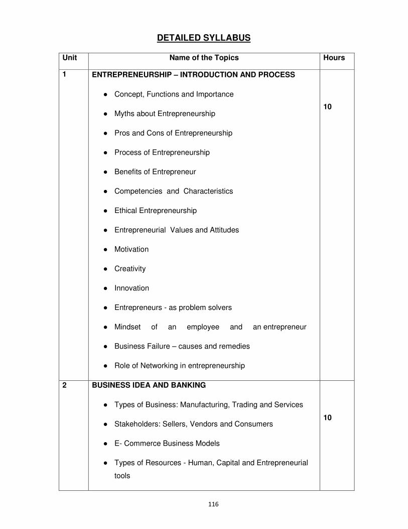
116
DETAILED SYLLABUS
Unit Name of the Topics Hours
1 ENTREPRENEURSHIP – INTRODUCTION AND PROCESS
● Concept, Functions and Importance
● Myths about Entrepreneurship
● Pros and Cons of Entrepreneurship
● Process of Entrepreneurship
● Benefits of Entrepreneur
● Competencies and Characteristics
● Ethical Entrepreneurship
● Entrepreneurial Values and Attitudes
● Motivation
● Creativity
● Innovation
● Entrepreneurs - as problem solvers
● Mindset of an employee and an entrepreneur
● Business Failure – causes and remedies
● Role of Networking in entrepreneurship
10
2 BUSINESS IDEA AND BANKING
● Types of Business: Manufacturing, Trading and Services
● Stakeholders: Sellers, Vendors and Consumers
● E- Commerce Business Models
● Types of Resources - Human, Capital and Entrepreneurial
tools
10
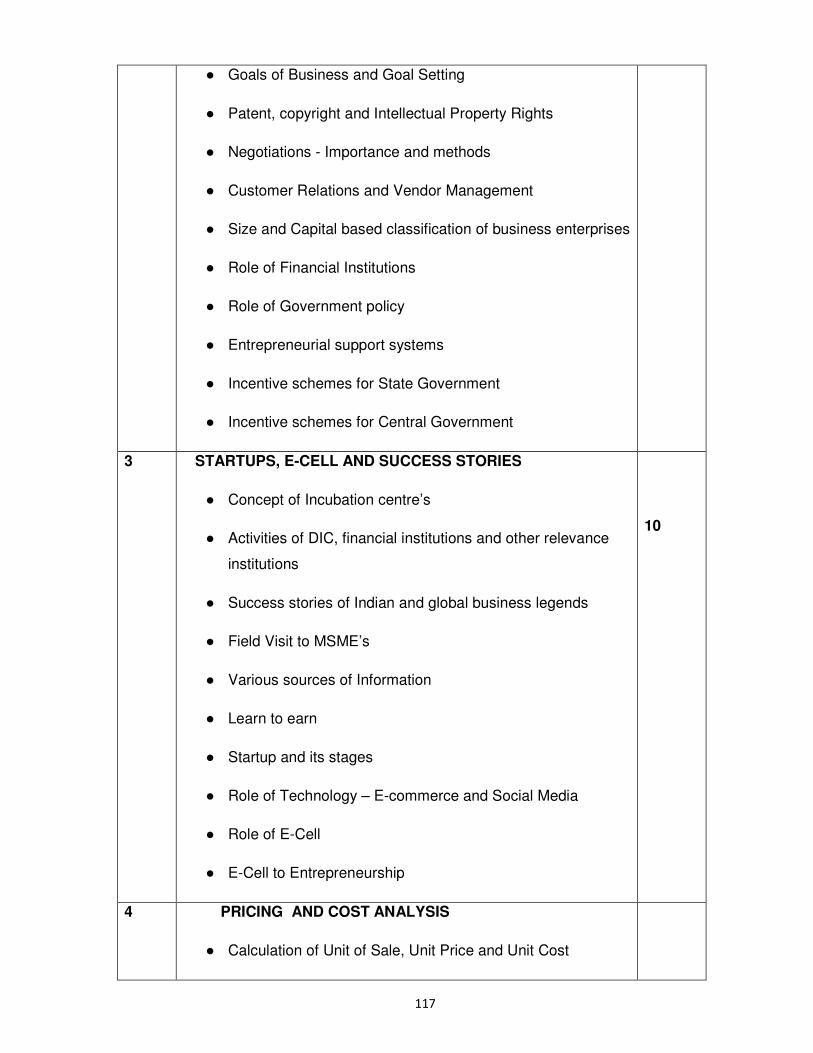
117
● Goals of Business and Goal Setting
● Patent, copyright and Intellectual Property Rights
● Negotiations - Importance and methods
● Customer Relations and Vendor Management
● Size and Capital based classification of business enterprises
● Role of Financial Institutions
● Role of Government policy
● Entrepreneurial support systems
● Incentive schemes for State Government
● Incentive schemes for Central Government
3 STARTUPS, E-CELL AND SUCCESS STORIES
● Concept of Incubation centre’s
● Activities of DIC, financial institutions and other relevance
institutions
● Success stories of Indian and global business legends
● Field Visit to MSME’s
● Various sources of Information
● Learn to earn
● Startup and its stages
● Role of Technology – E-commerce and Social Media
● Role of E-Cell
● E-Cell to Entrepreneurship
10
4 PRICING AND COST ANALYSIS
● Calculation of Unit of Sale, Unit Price and Unit Cost
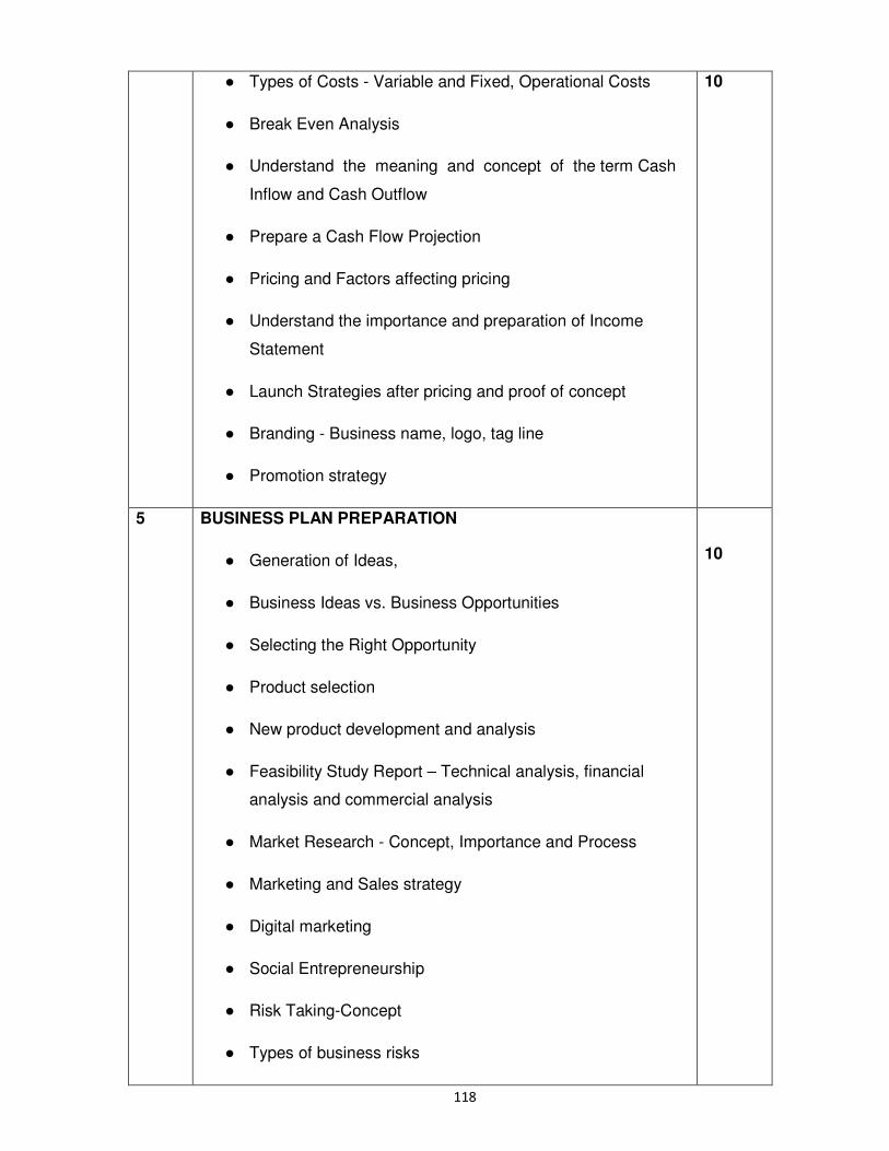
118
● Types of Costs - Variable and Fixed, Operational Costs
● Break Even Analysis
● Understand the meaning and concept of the term Cash
Inflow and Cash Outflow
● Prepare a Cash Flow Projection
● Pricing and Factors affecting pricing
● Understand the importance and preparation of Income
Statement
● Launch Strategies after pricing and proof of concept
● Branding - Business name, logo, tag line
● Promotion strategy
10
5 BUSINESS PLAN PREPARATION
● Generation of Ideas,
● Business Ideas vs. Business Opportunities
● Selecting the Right Opportunity
● Product selection
● New product development and analysis
● Feasibility Study Report – Technical analysis, financial
analysis and commercial analysis
● Market Research - Concept, Importance and Process
● Marketing and Sales strategy
● Digital marketing
● Social Entrepreneurship
● Risk Taking-Concept
● Types of business risks
10
119
REFERNCE BOOKS: 1. Dr. G.K. Varshney, Fundamentals of Entrepreneurship, Sahitya Bhawan Publications,
Agra - 282002
2. Dr. G.K. Varshney, Business Regulatory Framework , Sahitya Bhawan Publications,
Agra - 282002
3. Robert D. Hisrich, Michael P. Peters, Dean A. Shepherd, Entrepreneurship , McGraw
Hill (India) Private Limited, Noida - 201301
4. M.Scarborough, R.Cornwell, Essentials of Entrepreneurship and small business
management, Pearson Education India, Noida - 201301
5. Charantimath Poornima M. Entrepreneurship Development and Small Business
Enterprises, Pearson Education, Noida - 201301
6. Trott, Innovation Management and New Product Development, Pearson Education,
Noida - 201301
7. M N Arora, A Textbook of Cost and Management Accounting, Vikas Publishing House
Pvt. Ltd., New Delhi-110044
8. Prasanna Chandra, Financial Management, Tata McGraw Hill education private
limited, New Delhi
9. I. V. Trivedi, RenuJatana, Indian Banking System, RBSA Publishers, Rajasthan
10. Simon Daniel, HOW TO START A BUSINESS IN INDIA, BUUKS, Chennai - 600018
11. Ramani Sarada, The Business Plan Write-Up Simplified - A practitioners guide to
writing the Business Plan, Notion Press Media Pvt. Ltd., Chennai 600095.
Board Examination – Evaluation Pattern
Internal Mark Allocation
Assignment (Theory portion)* - 10
Seminar Presentation - 10
Attendance - 5
TOTAL - 25
Note: * Two assignments should be submitted. The same must be evaluated and
converted to 10 marks.
Guidelines for assignment:
First assignment – Unit I
Second assignment – Unit II
Guidelines for Seminar Presentation--Unit III
Each assignment should have five three marks questions and two five marks questions.
120
BOARD EXAMINATION
Note 1. The students should be taught all units and proper exposure and field visit also
arranged. All the portions should be completed before examinations.
2. The students should maintain theory assignment and seminar presentation.
The assignment and seminar presentation should be submitted during the
Board Practical Examinations.
3. The question paper consists of theory and practical portions. All students
should write the answers for theory questions (40 Marks) and practical
portions (60 Marks) should be completed for board examinations.
4. All exercises should be given in the question paper and students are allowed
to select by lot. If required the dimensions of the exercises may be varied for
every batch. No fixed time allotted for each portion and students have liberty to
do the examination for 3Hrs.
5. For Written Examination: theory question and answer: 45 Marks
Ten questions will be asked for 3 marks each. Five questions from each unit 1
& 2. (10 X 3 = 30).
Three questions will be asked for 5 marks each. One question from each unit
1, 2 & 3. (3 X 5 = 15)
6. For Practical Examination: The business plan/Feasibility report or Report on
Unit 4 & 5 should be submitted during the board practical examinations. The
same have to be evaluated for the report submission (40 marks).
DETAILED ALLOCATION OF MARKS
Sl.
No
Description Marks
Part A Written Examination - Theory Question and answer
(10 questions x 3 marks:30 marks & (3 questions x 5
marks: 15 marks)
45
Part B Practical Examination – Submission on Business
Plan/Feasibility Report or Report on Unit 4 & 5
40
Part C Viva voce 15
Total 100
121
STATE BOARD OF TECHNICAL EDUCATION & TRAINING, TAMILNADU
DIPLOMA IN ENGINEERING / TECHNOLOGY SYLLABUS
N-SCHEME
(To be Implementedfor the students admitted from the year 2020 - 2021 onwards)
Course Name : 1040:Electronics and Communication Engineering
Subject code : 4040610 Semester : VI Subject title : COMPUTER HARDWARE SERVICING AND NETWORKING
TEACHING AND SCHEME OF EXAMINATION
No. of Weeks per Semester: 16 Weeks
Subject
Instruction Examination
Hours
/week
Hours
/semester
Marks Duration
Internal Assessment
Board Examination
Total
Computer hardware Servicing and Networking
5
80
25
100*
100
3 Hours
* Examination will be conducted for 100 marks and it will be reduced to 75 marks.
Topics and Allocation of Hours
Unit Topics Hours
I MOTHERBOARD COMPONENTS AND MEMORY STORAGE DEVICES
16
II I/O DEVICES AND INTERFACE 14
III TROUBLE SHOOTING OF DESKTOP AND LAPTOPS 15
IV COMPUTER NETWORK DEVICES AND OSI LAYERS 14
V 802.X AND TCP/IP PROTOCOLS 14
Tests and Model 7
Total 80
122
RATIONALE:
Maintaining and servicing the computers, laptops and peripherals are essential
requirements of the computer students. The clear understanding of computer network
devices and protocols are also taught in this subject.
OBJECTIVES:
On completion of the following units of syllabus contents, the students can
� Identify the major components ofCPU.
� Understand the principle of operations of all the interfacing boards, IO/Memory
slots and interfacingdevices.
� Know the use of diagnostic Software.
� Trouble shoot the problems inLaptop.
� Understand the different layers of OSI and their functions. Compare different
LANprotocols.
� Identify the protocols used in TCP /IP and compare with OSI model. Use of IP
addressing and TCP/ IP protocolsbriefly.
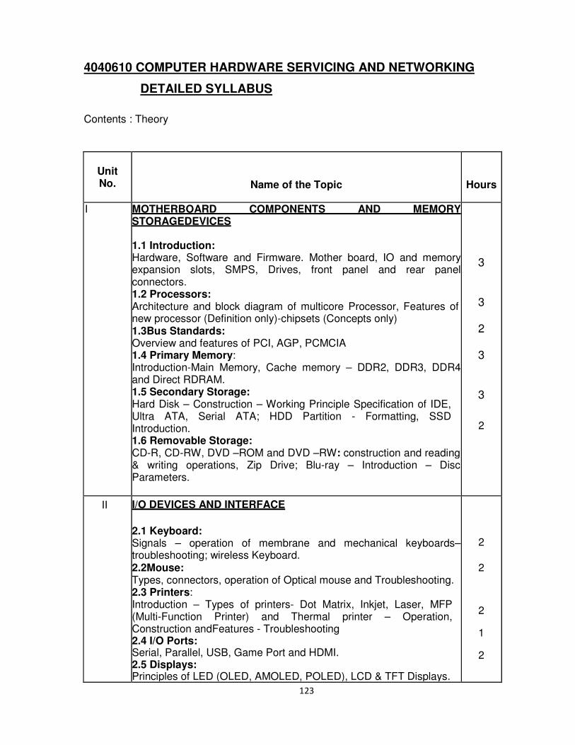
123
4040610 COMPUTER HARDWARE SERVICING AND NETWORKING
DETAILED SYLLABUS
Contents : Theory
Unit No.
Name of the Topic
Hours
I MOTHERBOARD COMPONENTS AND MEMORY STORAGEDEVICES 1.1 Introduction: Hardware, Software and Firmware. Mother board, IO and memory expansion slots, SMPS, Drives, front panel and rear panel connectors. 1.2 Processors: Architecture and block diagram of multicore Processor, Features of new processor (Definition only)-chipsets (Concepts only) 1.3Bus Standards: Overview and features of PCI, AGP, PCMCIA 1.4 Primary Memory: Introduction-Main Memory, Cache memory – DDR2, DDR3, DDR4 and Direct RDRAM. 1.5 Secondary Storage: Hard Disk – Construction – Working Principle Specification of IDE, Ultra ATA, Serial ATA; HDD Partition - Formatting, SSD Introduction. 1.6 Removable Storage: CD-R, CD-RW, DVD –ROM and DVD –RW: construction and reading & writing operations, Zip Drive; Blu-ray – Introduction – Disc Parameters.
3 3 2 3 3
2
II I/O DEVICES AND INTERFACE
2.1 Keyboard: Signals – operation of membrane and mechanical keyboards–troubleshooting; wireless Keyboard. 2.2Mouse: Types, connectors, operation of Optical mouse and Troubleshooting. 2.3 Printers: Introduction – Types of printers- Dot Matrix, Inkjet, Laser, MFP (Multi-Function Printer) and Thermal printer – Operation, Construction andFeatures - Troubleshooting 2.4 I/O Ports: Serial, Parallel, USB, Game Port and HDMI. 2.5 Displays: Principles of LED (OLED, AMOLED, POLED), LCD & TFT Displays.
2
2
2
1
2
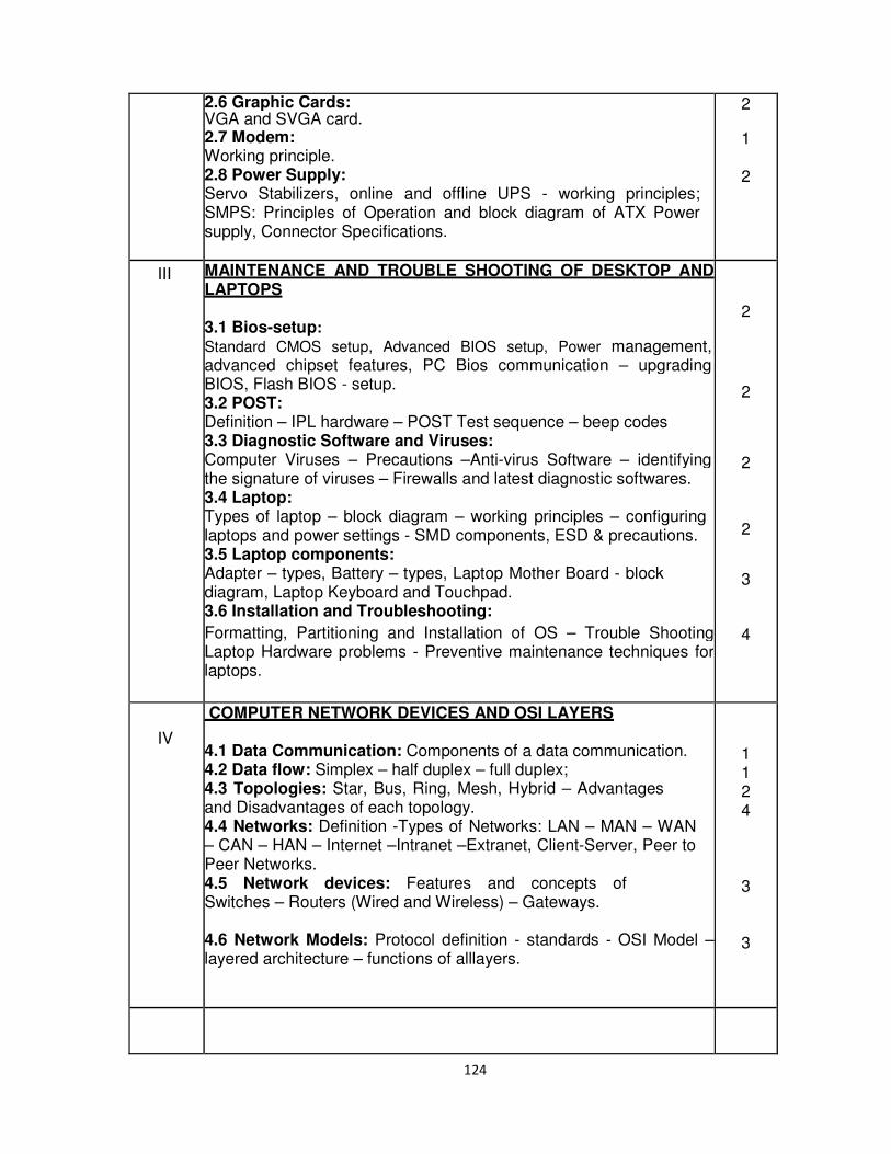
124
2.6 Graphic Cards: VGA and SVGA card. 2.7 Modem: Working principle. 2.8 Power Supply: Servo Stabilizers, online and offline UPS - working principles; SMPS: Principles of Operation and block diagram of ATX Power supply, Connector Specifications.
2
1 2
III MAINTENANCE AND TROUBLE SHOOTING OF DESKTOP AND LAPTOPS 3.1 Bios-setup:
Standard CMOS setup, Advanced BIOS setup, Power management, advanced chipset features, PC Bios communication – upgrading BIOS, Flash BIOS - setup. 3.2 POST: Definition – IPL hardware – POST Test sequence – beep codes 3.3 Diagnostic Software and Viruses: Computer Viruses – Precautions –Anti-virus Software – identifying the signature of viruses – Firewalls and latest diagnostic softwares. 3.4 Laptop: Types of laptop – block diagram – working principles – configuring laptops and power settings - SMD components, ESD & precautions. 3.5 Laptop components: Adapter – types, Battery – types, Laptop Mother Board - block diagram, Laptop Keyboard and Touchpad. 3.6 Installation and Troubleshooting:
Formatting, Partitioning and Installation of OS – Trouble Shooting Laptop Hardware problems - Preventive maintenance techniques for laptops.
2 2
2
2
3
4
IV
COMPUTER NETWORK DEVICES AND OSI LAYERS 4.1 Data Communication: Components of a data communication. 4.2 Data flow: Simplex – half duplex – full duplex; 4.3 Topologies: Star, Bus, Ring, Mesh, Hybrid – Advantages and Disadvantages of each topology. 4.4 Networks: Definition -Types of Networks: LAN – MAN – WAN – CAN – HAN – Internet –Intranet –Extranet, Client-Server, Peer to Peer Networks. 4.5 Network devices: Features and concepts of Switches – Routers (Wired and Wireless) – Gateways. 4.6 Network Models: Protocol definition - standards - OSI Model –layered architecture – functions of alllayers.
1 1 2 4 3 3
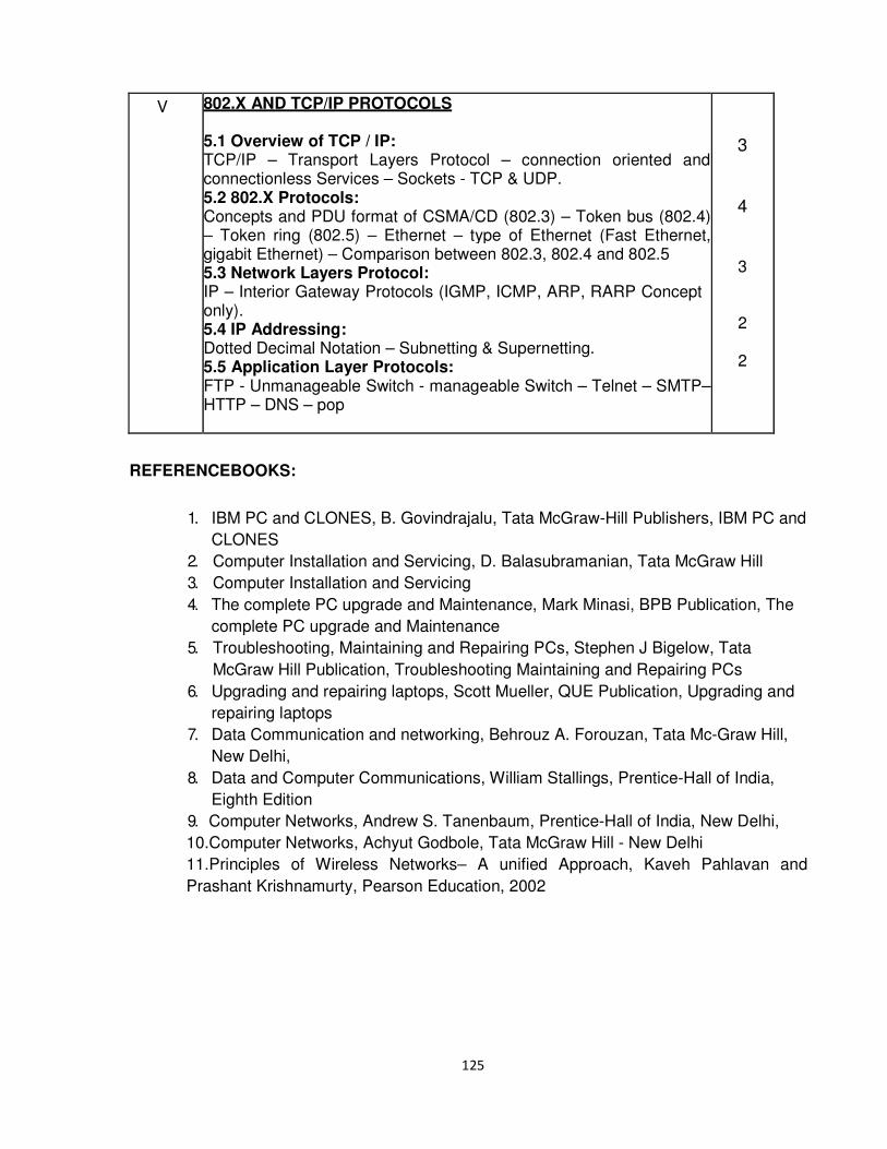
125
REFERENCEBOOKS:
1. IBM PC and CLONES, B. Govindrajalu, Tata McGraw-Hill Publishers, IBM PC and
CLONES
2. Computer Installation and Servicing, D. Balasubramanian, Tata McGraw Hill
3. Computer Installation and Servicing
4. The complete PC upgrade and Maintenance, Mark Minasi, BPB Publication, The
complete PC upgrade and Maintenance
5. Troubleshooting, Maintaining and Repairing PCs, Stephen J Bigelow, Tata
McGraw Hill Publication, Troubleshooting Maintaining and Repairing PCs
6. Upgrading and repairing laptops, Scott Mueller, QUE Publication, Upgrading and
repairing laptops
7. Data Communication and networking, Behrouz A. Forouzan, Tata Mc-Graw Hill,
New Delhi,
8. Data and Computer Communications, William Stallings, Prentice-Hall of India,
Eighth Edition
9. Computer Networks, Andrew S. Tanenbaum, Prentice-Hall of India, New Delhi,
10.Computer Networks, Achyut Godbole, Tata McGraw Hill - New Delhi
11.Principles of Wireless Networks– A unified Approach, Kaveh Pahlavan and
Prashant Krishnamurty, Pearson Education, 2002
V 802.X AND TCP/IP PROTOCOLS 5.1 Overview of TCP / IP: TCP/IP – Transport Layers Protocol – connection oriented and connectionless Services – Sockets - TCP & UDP. 5.2 802.X Protocols: Concepts and PDU format of CSMA/CD (802.3) – Token bus (802.4) – Token ring (802.5) – Ethernet – type of Ethernet (Fast Ethernet, gigabit Ethernet) – Comparison between 802.3, 802.4 and 802.5 5.3 Network Layers Protocol: IP – Interior Gateway Protocols (IGMP, ICMP, ARP, RARP Concept only). 5.4 IP Addressing: Dotted Decimal Notation – Subnetting & Supernetting. 5.5 Application Layer Protocols: FTP - Unmanageable Switch - manageable Switch – Telnet – SMTP–HTTP – DNS – pop
3 4 3 2 2
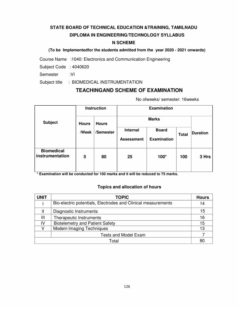
126
STATE BOARD OF TECHNICAL EDUCATION &TRAINING, TAMILNADU
DIPLOMA IN ENGINEERING/TECHNOLOGY SYLLABUS
N SCHEME
(To be Implementedfor the students admitted from the year 2020 - 2021 onwards)
Course Name :1040: Electronics and Communication Engineering
Subject Code : 4040620
Semester :VI
Subject title : BIOMEDICAL INSTRUMENTATION
TEACHINGAND SCHEME OF EXAMINATION
No ofweeks/ semester: 16weeks
Subject
Instruction Examination
Hours
/Week
Hours
/Semester
Marks Duration
Internal
Assessment
Board
Examination
Total
Biomedical instrumentation
5
80
25
100*
100
3 Hrs
* Examination will be conducted for 100 marks and it will be reduced to 75 marks.
Topics and allocation of hours
UNIT TOPIC Hours
I Bio-electric potentials, Electrodes and Clinical measurements 14
II Diagnostic Instruments 15
III Therapeutic Instruments 16
IV Biotelemetry and Patient Safety 15 V Modern Imaging Techniques 13
Tests and Model Exam 7
Total 80
127
RATIONALE:
Every year,thereisatremendousincreaseintheuseof Modern Electronic
medicalequipment inthehospitalandhealthcareindustry. Thereforeitisnecessary forevery
student ttounderstandthe functioning of various medical equipments.
OBJECTIVES:
After learning this subject the studentwill beable to understand the about
� The generation ofBio-potential and its measurement using various
electrodes.
� The measurement ofblood pressure.
� The measurement oflung volume.
� The measurement ofrespiration rate.
� The measurement ofbodytemperature and skin temperature.
� The principleofoperation ofECG recorder and the analysis of ECG waves
� The principle ofoperationofEEG recorder and the analysis of EEG waves
� The principle ofoperation ofEMG recorder.
� Theworking principles of audio meter.
� The principleofoperation ofpacemaker.
� The basic principle ofdialysis.
� The basic principle ofventilators.
� Theworking principles of telemetry.
� The basic principle oftelemedicine.
� To learn about patient safety.
� The various methods ofaccident prevention.
� The basic principle ofvarious types oflasers and their applications
� The basic principle of various types of Medical Imaging Systems.
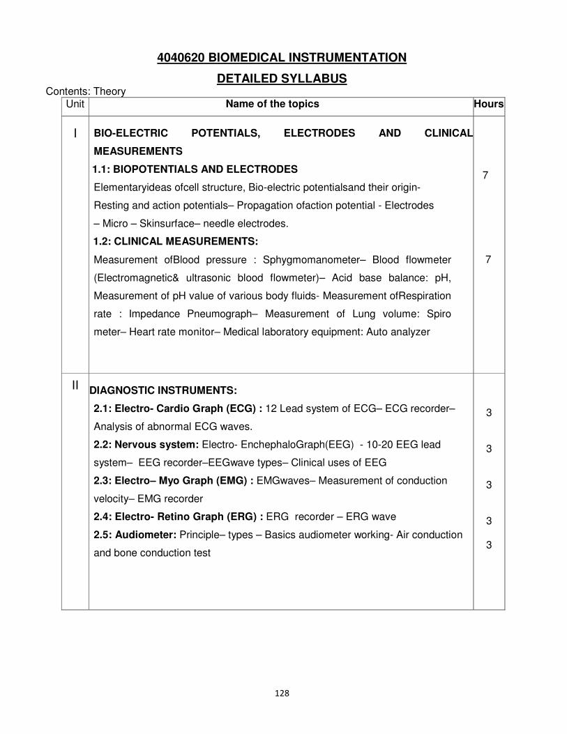
128
4040620 BIOMEDICAL INSTRUMENTATION
DETAILED SYLLABUS Contents: Theory
Unit Name of the topics Hours
I
BIO-ELECTRIC POTENTIALS, ELECTRODES AND CLINICAL
MEASUREMENTS
1.1: BIOPOTENTIALS AND ELECTRODES
Elementaryideas ofcell structure, Bio-electric potentialsand their origin-
Resting and action potentials– Propagation ofaction potential - Electrodes
– Micro – Skinsurface– needle electrodes.
1.2: CLINICAL MEASUREMENTS:
Measurement ofBlood pressure : Sphygmomanometer– Blood flowmeter
(Electromagnetic& ultrasonic blood flowmeter)– Acid base balance: pH,
Measurement of pH value of various body fluids- Measurement ofRespiration
rate : Impedance Pneumograph– Measurement of Lung volume: Spiro
meter– Heart rate monitor– Medical laboratory equipment: Auto analyzer
7 7
II
DIAGNOSTIC INSTRUMENTS:
2.1: Electro- Cardio Graph (ECG) : 12 Lead system of ECG– ECG recorder–
Analysis of abnormal ECG waves.
2.2: Nervous system: Electro- EnchephaloGraph(EEG) - 10-20 EEG lead
system– EEG recorder–EEGwave types– Clinical uses of EEG
2.3: Electro– Myo Graph (EMG) : EMGwaves– Measurement of conduction
velocity– EMG recorder
2.4: Electro- Retino Graph (ERG) : ERG recorder – ERG wave
2.5: Audiometer: Principle– types – Basics audiometer working- Air conduction
and bone conduction test
3 3 3 3 3
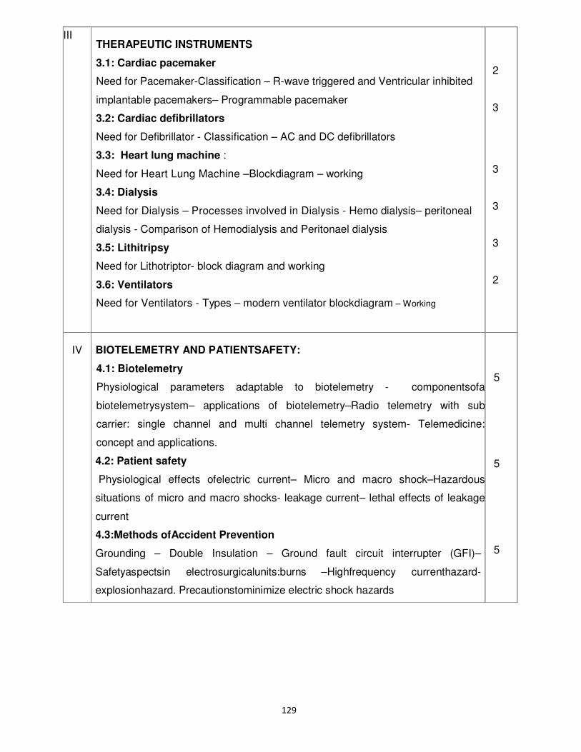
129
III THERAPEUTIC INSTRUMENTS
3.1: Cardiac pacemaker
Need for Pacemaker-Classification – R-wave triggered and Ventricular inhibited
implantable pacemakers– Programmable pacemaker
3.2: Cardiac defibrillators
Need for Defibrillator - Classification – AC and DC defibrillators
3.3: Heart lung machine :
Need for Heart Lung Machine –Blockdiagram – working
3.4: Dialysis
Need for Dialysis – Processes involved in Dialysis - Hemo dialysis– peritoneal
dialysis - Comparison of Hemodialysis and Peritonael dialysis
3.5: Lithitripsy
Need for Lithotriptor- block diagram and working
3.6: Ventilators
Need for Ventilators - Types – modern ventilator blockdiagram – Working
2 3 3 3 3 2
IV
BIOTELEMETRY AND PATIENTSAFETY:
4.1: Biotelemetry
Physiological parameters adaptable to biotelemetry - componentsofa
biotelemetrysystem– applications of biotelemetry–Radio telemetry with sub
carrier: single channel and multi channel telemetry system- Telemedicine:
concept and applications.
4.2: Patient safety
Physiological effects ofelectric current– Micro and macro shock–Hazardous
situations of micro and macro shocks- leakage current– lethal effects of leakage
current
4.3:Methods ofAccident Prevention
Grounding – Double Insulation – Ground fault circuit interrupter (GFI)–
Safetyaspectsin electrosurgicalunits:burns –Highfrequency currenthazard-
explosionhazard. Precautionstominimize electric shock hazards
5 5 5
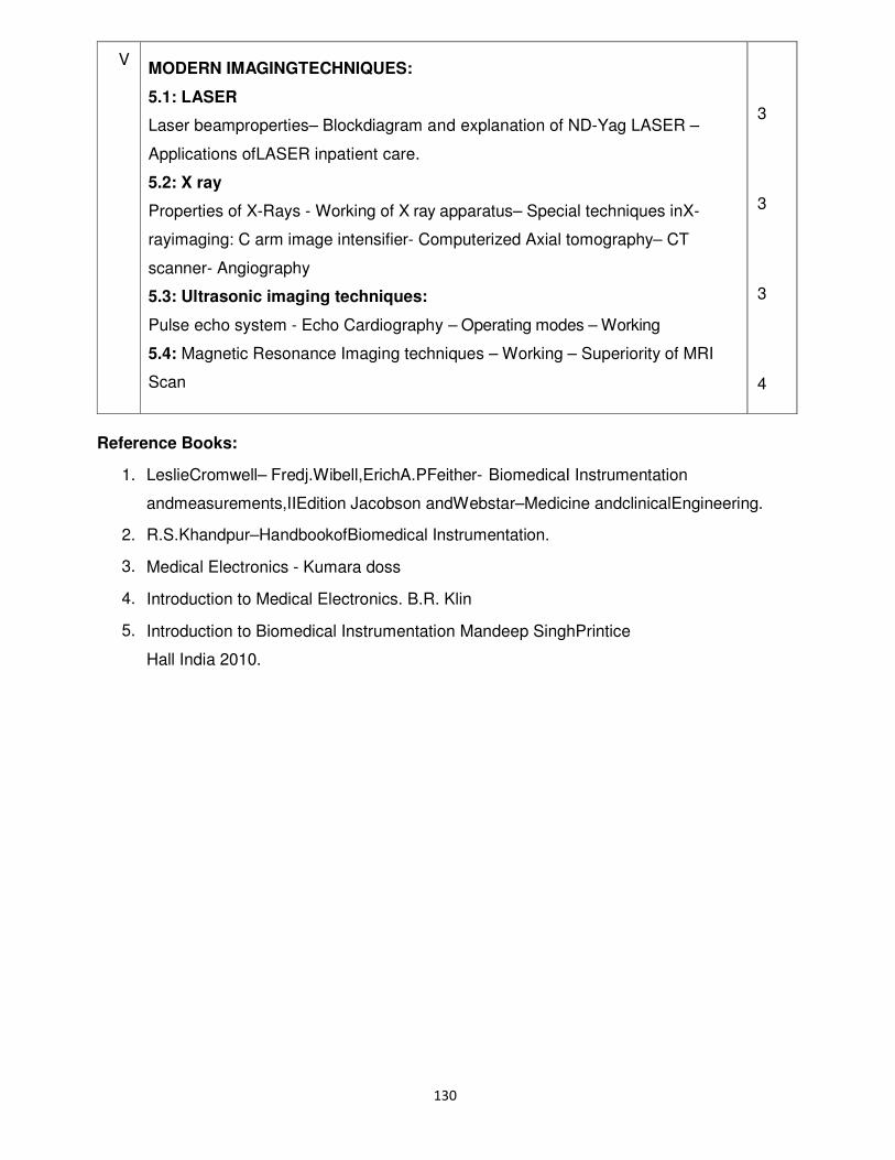
130
V MODERN IMAGINGTECHNIQUES:
5.1: LASER
Laser beamproperties– Blockdiagram and explanation of ND-Yag LASER –
Applications ofLASER inpatient care.
5.2: X ray
Properties of X-Rays - Working of X ray apparatus– Special techniques inX-
rayimaging: C arm image intensifier- Computerized Axial tomography– CT
scanner- Angiography
5.3: Ultrasonic imaging techniques:
Pulse echo system - Echo Cardiography – Operating modes – Working
5.4: Magnetic Resonance Imaging techniques – Working – Superiority of MRI
Scan
3
3
3
4
Reference Books:
1. LeslieCromwell– Fredj.Wibell,ErichA.PFeither- BiomedicaI Instrumentation
andmeasurements,IIEdition Jacobson andWebstar–Medicine andclinicalEngineering.
2. R.S.Khandpur–HandbookofBiomedical Instrumentation.
3. Medical Electronics - Kumara doss
4. Introduction to Medical Electronics. B.R. Klin
5. Introduction to Biomedical Instrumentation Mandeep SinghPrintice
Hall India 2010.
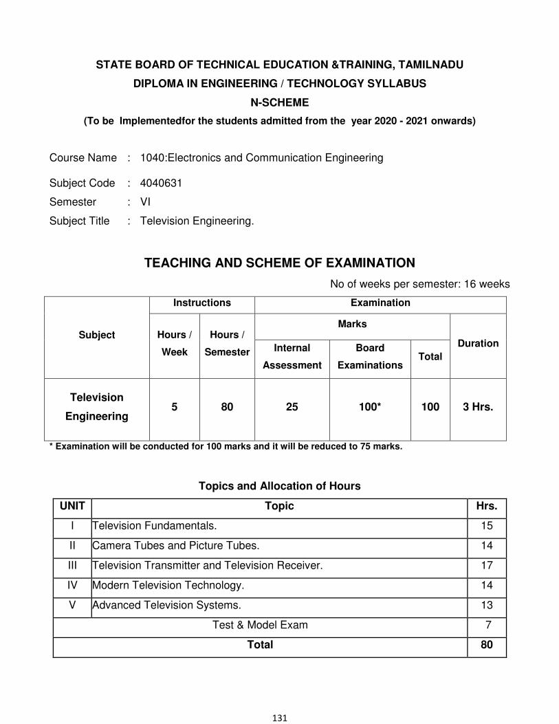
131
STATE BOARD OF TECHNICAL EDUCATION &TRAINING, TAMILNADU
DIPLOMA IN ENGINEERING / TECHNOLOGY SYLLABUS
N-SCHEME
(To be Implementedfor the students admitted from the year 2020 - 2021 onwards)
Course Name : 1040:Electronics and Communication Engineering Subject Code : 4040631
Semester : VI
Subject Title : Television Engineering.
TEACHING AND SCHEME OF EXAMINATION
No of weeks per semester: 16 weeks
Subject
Instructions Examination
Hours /
Week
Hours /
Semester
Marks
Duration Internal
Assessment
Board
Examinations Total
Television
Engineering 5 80 25 100* 100 3 Hrs.
* Examination will be conducted for 100 marks and it will be reduced to 75 marks.
Topics and Allocation of Hours
UNIT Topic Hrs.
I Television Fundamentals. 15
II Camera Tubes and Picture Tubes. 14
III Television Transmitter and Television Receiver. 17
IV Modern Television Technology. 14
V Advanced Television Systems. 13
Test & Model Exam 7
Total 80
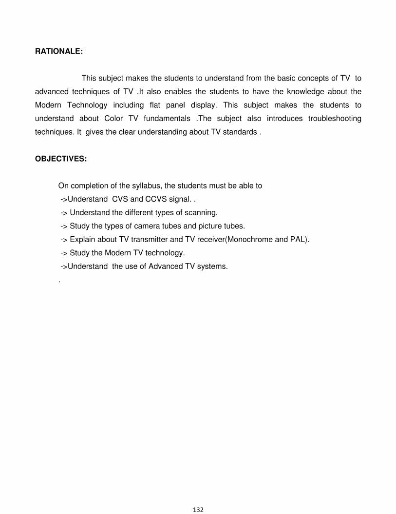
132
RATIONALE:
This subject makes the students to understand from the basic concepts of TV to
advanced techniques of TV .It also enables the students to have the knowledge about the
Modern Technology including flat panel display. This subject makes the students to
understand about Color TV fundamentals .The subject also introduces troubleshooting
techniques. It gives the clear understanding about TV standards .
OBJECTIVES:
On completion of the syllabus, the students must be able to
->Understand CVS and CCVS signal. .
-> Understand the different types of scanning.
-> Study the types of camera tubes and picture tubes.
-> Explain about TV transmitter and TV receiver(Monochrome and PAL).
-> Study the Modern TV technology.
->Understand the use of Advanced TV systems.
.
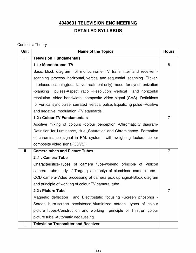
133
4040631 TELEVISION ENGINEERING
DETAILED SYLLABUS
Contents: Theory
Unit Name of the Topics Hours
I Television Fundamentals
1.1 : Monochrome TV
Basic block diagram of monochrome TV transmitter and receiver -
scanning process -horizontal, vertical and sequential scanning -Flicker-
Interlaced scanning(qualitative treatment only) -need for synchronization
-blanking pulses-Aspect ratio -Resolution -vertical and horizontal
resolution -video bandwidth -composite video signal (CVS) -Definitions
for vertical sync pulse, serrated vertical pulse, Equalizing pulse -Positive
and negative modulation -TV standards .
1.2 : Colour TV Fundamentals
Additive mixing of colours -colour perception -Chromaticity diagram-
Definition for Luminance, Hue ,Saturation and Chrominance- Formation
of chrominance signal in PAL system with weighting factors- colour
composite video signal(CCVS).
8
7
II Camera tubes and Picture Tubes
2..1 : Camera Tube
Characteristics-Types of camera tube-working principle of Vidicon
camera tube-study of Target plate (only) of plumbicon camera tube -
CCD camera-Video processing of camera pick up signal-Block diagram
and principle of working of colour TV camera tube.
2.2 : Picture Tube
Magnetic deflection and Electrostatic focusing -Screen phosphor -
Screen burn-screen persistence-Aluminized screen- types of colour
picture tubes-Construction and working principle of Trinitron colour
picture tube -Automatic degaussing.
7
7
III Television Transmitter and Receiver
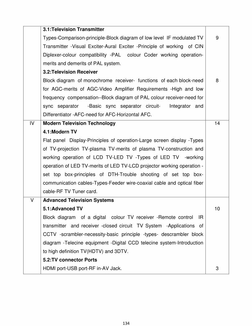
134
3.1:Television Transmitter
Types-Comparison-principle-Block diagram of low level IF modulated TV
Transmitter -Visual Exciter-Aural Exciter -Principle of working of CIN
Diplexer-colour compatibility -PAL colour Coder working operation-
merits and demerits of PAL system.
3.2:Television Receiver
Block diagram of monochrome receiver- functions of each block-need
for AGC-merits of AGC-Video Amplifier Requirements -High and low
frequency compensation--Block diagram of PAL colour receiver-need for
sync separator -Basic sync separator circuit- Integrator and
Differentiator -AFC-need for AFC-Horizontal AFC.
9
8
IV Modern Television Technology
4.1:Modern TV
Flat panel Display-Principles of operation-Large screen display -Types
of TV-projection TV-plasma TV-merits of plasma TV-construction and
working operation of LCD TV-LED TV -Types of LED TV -working
operation of LED TV-merits of LED TV-LCD projector working operation -
set top box-principles of DTH-Trouble shooting of set top box-
communication cables-Types-Feeder wire-coaxial cable and optical fiber
cable-RF TV Tuner card.
14
V Advanced Television Systems
5.1:Advanced TV
Block diagram of a digital colour TV receiver -Remote control IR
transmitter and receiver -closed circuit TV System -Applications of
CCTV -scrambler-necessity-basic principle -types- descrambler block
diagram -Telecine equipment -Digital CCD telecine system-Introduction
to high definition TV(HDTV) and 3DTV.
5.2:TV connector Ports
HDMI port-USB port-RF in-AV Jack.
10
3
135
Reference Books:
1.”R.R. Gulati”,”Modern Television Practice-Transmission,Reception,Applications “,New age
international 5th Edition 2015.
2.”A.M.Dhake” “TV and Video Engineering” ,Second Edition TMH-2003
3.”R.R Gulati” “Monochrome and Color TV “, New Age Publishers-2003
4.”S.P.bali” “color TV, Theory and Practice” TMH-1994.
5.” Manohar Lotia& Pradeep Nair “ “Modern VCD-Video CD player Introduction, servicing and
troubleshooting “,BPB Publications 2002
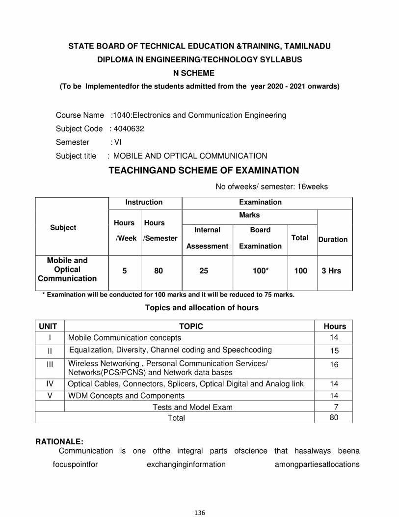
136
STATE BOARD OF TECHNICAL EDUCATION &TRAINING, TAMILNADU
DIPLOMA IN ENGINEERING/TECHNOLOGY SYLLABUS
N SCHEME
(To be Implementedfor the students admitted from the year 2020 - 2021 onwards)
Course Name :1040:Electronics and Communication Engineering
Subject Code : 4040632
Semester : VI
Subject title : MOBILE AND OPTICAL COMMUNICATION
TEACHINGAND SCHEME OF EXAMINATION
No ofweeks/ semester: 16weeks
Subject
Instruction Examination
Hours
/Week
Hours
/Semester
Marks Duration
Internal Assessment
Board
Examination
Total
Mobile and Optical
Communication
5
80
25
100*
100
3 Hrs
* Examination will be conducted for 100 marks and it will be reduced to 75 marks.
Topics and allocation of hours
UNIT TOPIC Hours
I Mobile Communication concepts 14
II Equalization, Diversity, Channel coding and Speechcoding 15
III Wireless Networking , Personal Communication Services/ Networks(PCS/PCNS) and Network data bases
16
IV Optical Cables, Connectors, Splicers, Optical Digital and Analog link 14
V WDM Concepts and Components 14 Tests and Model Exam 7
Total 80
RATIONALE:
Communication is one ofthe integral parts ofscience that hasalways beena
focuspointfor exchanginginformation amongpartiesatlocations
137
physicallyapart.Afteritsdiscovery, telephones havereplacedthetelegrams
andletters.Similarly,theterm‘mobile’hascompletely revolutionizedthe communicationby
openingupinnovativeapplicationsthatarelimitedtoone’s
imagination.Today,mobilecommunicationhas becomethebackboneofthe society.Allthe
mobile systemtechnologieshaveimprovedtheway ofliving.Usually Mobile cellular
networks have both Circuit Switching and Packet Switching for handling calls. For Circuit
Switching ,Optical fiber using WDM is employed. Hence inthis subject, with Mobile
communication , Optical communication is added.
OBJECTIVES:
On completion ofthefollowing units of syllabus contents, the students must be
able to:
� Know the concept of Mobile Communication
� Know the concept of Channel Assignments
� Know aboutthe Handoff processes performed in Mobile Communication
� Know the interferences and system capacity
� Know the methods of improving coverage and capacity to avoid network
congestion
� Know the concept of equalization, diversity , channel coding and speech coding
� Know the concept of LTE and VoLTE (Voice over Long Term Evolution
� Know about wireless networking , Personal Communication Services/
Networks(PCS/PCNS) and network data bases
� Know about Universal Mobile Telecommunication System (UMTS)
� Know about Fiber optic cables
� Know about Power launching and coupling
� Know about Fiber-to-fiber joints
� Know about Fiber splicing techniques
� Know aboutOptical fiber connectors
� Know about Digital transmission systems
� Know about WDMconcepts and components
� Know about Opticalnetworks
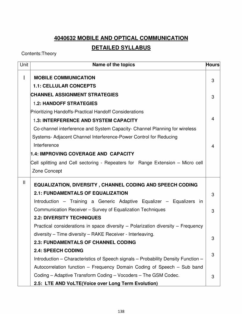
138
4040632 MOBILE AND OPTICAL COMMUNICATION
DETAILED SYLLABUS Contents:Theory
Unit Name of the topics Hours
I
MOBILE COMMUNICATION
1.1: CELLULAR CONCEPTS
CHANNEL ASSIGNMENT STRATEGIES
1.2: HANDOFF STRATEGIES
Prioritizing Handoffs-Practical Handoff Considerations
1.3: INTERFERENCE AND SYSTEM CAPACITY
Co-channel interference and System Capacity- Channel Planning for wireless
Systems- Adjacent Channel Interference-Power Control for Reducing
Interference
1.4: IMPROVING COVERAGE AND CAPACITY
Cell splitting and Cell sectoring - Repeaters for Range Extension – Micro cell
Zone Concept
3
3
4
4
II EQUALIZATION, DIVERSITY , CHANNEL CODING AND SPEECH CODING
2.1: FUNDAMENTALS OF EQUALIZATION
Introduction – Training a Generic Adaptive Equalizer – Equalizers in
Communication Receiver – Survey of Equalization Techniques
2.2: DIVERSITY TECHNIQUES
Practical considerations in space diversity – Polarization diversity – Frequency
diversity – Time diversity – RAKE Receiver - Interleaving.
2.3: FUNDAMENTALS OF CHANNEL CODING
2.4: SPEECH CODING
Introduction – Characteristics of Speech signals – Probability Density Function –
Autocorrelation function – Frequency Domain Coding of Speech – Sub band
Coding – Adaptive Transform Coding – Vocoders – The GSM Codec.
2.5: LTE AND VoLTE(Voice over Long Term Evolution)
3
3
3
3
3

139
III
WIRELESS NETWORKING , PERSONAL COMMUNICATION SERVICES/
NETWORKS(PCS/PCNs) AND NETWORK DATA BASES
3.1: INTRODUCTION TO WIRELESS NETWORKS
3.2: DIFFERENCE BETWEEN WIRELESS NETWORKS AND FIXED
NETWORKS
Limitations in wireless networking – Merging wireless network and PSTN
Development of Wireless Networks
3.3: WIRELESS DATA SERVICES
Cellular Digital Packet Data (CDPD) – Advanced Radio Data Information
Systems (ARDIS) – RAM Mobile Data (RMD)
3.4: PERSONAL COMMUNICATION SERVICES/ NETWORKS(PCS/PCNs)
Packet Vs Circuit Switching for PCN – Cellular Packet Switched Architecture
3.5: NETWORK DATABASES
Distributed Database for Mobility Management
3.6:UNIVERSAL MOBILE TELECOMMUNICATION SYSTEM (UMTS)
3
3
3
3
2
2
IV
OPTICAL COMMUNICATION
4.1: FIBER OPTIC CABLES
4.2: POWER LAUNCHING AND COUPLING
Source to Fiber Power Launching - Source Output Pattern- Schematic diagram of
an optical source coupled to an optical fiber-Lensing scheme for coupling
improvement
4.3: FIBER-TO-FIBER JOINTS
4.3: FIBER SPLICING TECHNIQUES
4.4: OPTICAL FIBER CONNECTORS
4.5: DIGITAL TRANSMISSION SYSTEMS
Simplex point to point transmission link – System consideration
4.6: ANALOG TRANSMISSION SYSTEMS
Over view of Analog links
2
3
2
2
2
3
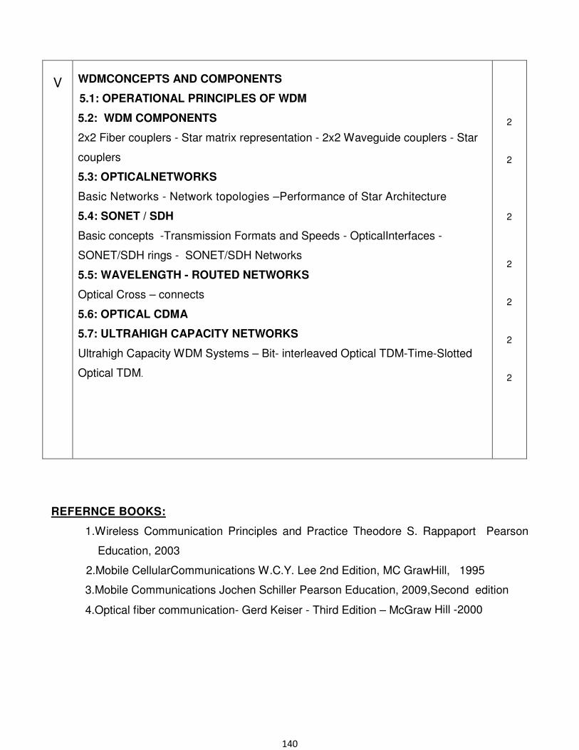
140
V WDMCONCEPTS AND COMPONENTS
5.1: OPERATIONAL PRINCIPLES OF WDM
5.2: WDM COMPONENTS
2x2 Fiber couplers - Star matrix representation - 2x2 Waveguide couplers - Star
couplers
5.3: OPTICALNETWORKS
Basic Networks - Network topologies –Performance of Star Architecture
5.4: SONET / SDH
Basic concepts -Transmission Formats and Speeds - OpticalInterfaces -
SONET/SDH rings - SONET/SDH Networks
5.5: WAVELENGTH - ROUTED NETWORKS
Optical Cross – connects
5.6: OPTICAL CDMA
5.7: ULTRAHIGH CAPACITY NETWORKS
Ultrahigh Capacity WDM Systems – Bit- interleaved Optical TDM-Time-Slotted
Optical TDM.
2
2
2
2
2
2
2
REFERNCE BOOKS:
1.Wireless Communication Principles and Practice Theodore S. Rappaport Pearson
Education, 2003
2.Mobile CellularCommunications W.C.Y. Lee 2nd Edition, MC GrawHill, 1995
3.Mobile Communications Jochen Schiller Pearson Education, 2009,Second edition
4.Optical fiber communication- Gerd Keiser - Third Edition – McGraw Hill -2000
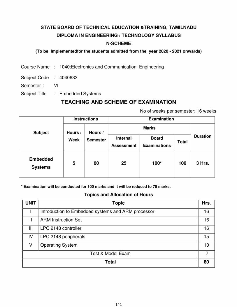
141
STATE BOARD OF TECHNICAL EDUCATION &TRAINING, TAMILNADU
DIPLOMA IN ENGINEERING / TECHNOLOGY SYLLABUS
N-SCHEME
(To be Implementedfor the students admitted from the year 2020 - 2021 onwards)
Course Name : 1040:Electronics and Communication Engineering Subject Code : 4040633
Semester : VI
Subject Title : Embedded Systems
TEACHING AND SCHEME OF EXAMINATION
No of weeks per semester: 16 weeks
Subject
Instructions Examination
Hours /
Week
Hours /
Semester
Marks
Duration Internal
Assessment
Board
Examinations Total
Embedded
Systems 5 80 25 100* 100 3 Hrs.
* Examination will be conducted for 100 marks and it will be reduced to 75 marks.
Topics and Allocation of Hours
UNIT Topic Hrs.
I Introduction to Embedded systems and ARM processor 16
II ARM Instruction Set 16
III LPC 2148 controller 16
IV LPC 2148 peripherals 15
V Operating System 10
Test & Model Exam 7
Total 80
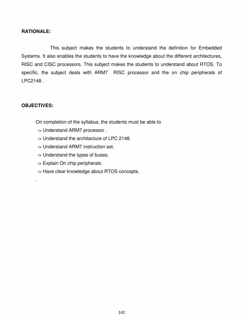
142
RATIONALE:
This subject makes the students to understand the definition for Embedded
Systems. It also enables the students to have the knowledge about the different architectures,
RISC and CISC processors. This subject makes the students to understand about RTOS. To
specific, the subject deals with ARM7 RISC processor and the on chip peripherals of
LPC2148 .
OBJECTIVES:
On completion of the syllabus, the students must be able to
-> Understand ARM7 processor .
-> Understand the architecture of LPC 2148.
-> Understand ARM7 instruction set.
-> Understand the types of buses.
-> Explain On chip peripherals.
-> Have clear knowledge about RTOS concepts.
.
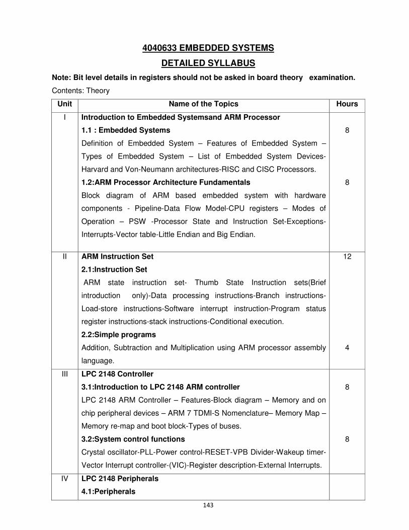
143
4040633 EMBEDDED SYSTEMS
DETAILED SYLLABUS
Note: Bit level details in registers should not be asked in board theory examination.
Contents: Theory
Unit Name of the Topics Hours
I Introduction to Embedded Systemsand ARM Processor
1.1 : Embedded Systems
Definition of Embedded System – Features of Embedded System –
Types of Embedded System – List of Embedded System Devices-
Harvard and Von-Neumann architectures-RISC and CISC Processors.
1.2:ARM Processor Architecture Fundamentals
Block diagram of ARM based embedded system with hardware
components - Pipeline-Data Flow Model-CPU registers – Modes of
Operation – PSW -Processor State and Instruction Set-Exceptions-
Interrupts-Vector table-Little Endian and Big Endian.
8
8
II ARM Instruction Set
2.1:Instruction Set
ARM state instruction set- Thumb State Instruction sets(Brief
introduction only)-Data processing instructions-Branch instructions-
Load-store instructions-Software interrupt instruction-Program status
register instructions-stack instructions-Conditional execution.
2.2:Simple programs
Addition, Subtraction and Multiplication using ARM processor assembly
language.
12
4
III LPC 2148 Controller
3.1:Introduction to LPC 2148 ARM controller
LPC 2148 ARM Controller – Features-Block diagram – Memory and on
chip peripheral devices – ARM 7 TDMI-S Nomenclature– Memory Map –
Memory re-map and boot block-Types of buses.
3.2:System control functions
Crystal oscillator-PLL-Power control-RESET-VPB Divider-Wakeup timer-
Vector Interrupt controller-(VIC)-Register description-External Interrupts.
8
8
IV LPC 2148 Peripherals
4.1:Peripherals
144
Pin connect block-Features-pin connect block register description-GPIO
(Slow)- Features-register description -- Timer/Counter – Block diagram –
Register description --PWM-features-register description-ADC -features-
register description-DAC-features-register description.
4.2:Serial communication in LPC 2148
UART features – UART0 Block diagram—UART0 register description.
10
5
V Operating System
5.1:Embedded OS and RTOS
Introduction to OS- -Functions of OS-Embedded OS-
Foreground/background systems -Real time system concepts-
Resources-shared resources-Critical section- multitasking-Tasks-kernel-
Scheduler-Round Robin-Non Pre-emptive and Pre-emptive scheduling-
Context switch- re-entrancy- task priorities- Event flag-mutual exclusion-
semaphores and types-Message mail box-Message Queues.
10
Reference Books
1.”Andrew N Sloss””ARM System Developer’s Guide Designing and Optimizing” Elsevier
publication,2004.
2.”B.Kanta Rao” “Embedded systems”, PHI publishers.
3.”TammyNoergaard” “Embedded Systems Architecture”,Newness edition.
4.”SteveFurbe “ “ARM System on chip Architecture”, 2ndedition,Pearson Education,2000.
5.”Dr.K.V.K.K Prasad””Embedded Real Time Systems”,Dream tech press,2009.
6.”David Seal” “ARM Architecture Reference Manual”.
7.LPC 2148 User Manual.
145
STATE BOARD OF TECHNICAL EDUCATION &TRAINING, TAMILNADU
DIPLOMA IN ENGINEERING / TECHNOLOGY SYLLABUS
N-SCHEME
(To be Implementedfor the students admitted from the year 2020 - 2021 onwards)
Course Name : 1040:Electronics and Communication Engineering
Subject Code : 4040640
Semester : VI Semester
Subject Title : COMPUTER HARDWARE SERVICING AND
NETWORKING PRACTICAL
TEACHING AND SCHEME OF EXAMINATION
No. of weeks per semester: 16 weeks
Subject
Instructions Examination
Hours /
Week
Hours /
Semester
Marks
Duration Internal
Assessment
Board
Examinations Total
Computer
Hardware
Servicing and
Networking
Practical
6 96 25 100* 100 3 Hrs.
* Examination will be conducted for 100 marks and it will be reduced to 75 marks.
RATIONALE:
The course aims at making the students familiar with various parts of computers
and laptops and how to assemble them and the different types of peripherals desired.
In addition, the course will provide the students with necessary knowledge and skills in
computer and laptop software installation and maintenance and to make him diagnose
the software faults. This subject also gives the knowledge and competency to diagnose
the problems in computer hardware and peripherals and gives the knowledge for
trouble shooting for systematic repair and maintenance of computers and laptops
146
OBJECTIVES:
On completion of the following exercises, the students must be able to
� Know the various indicators, switches, SMPS,motherboard
,connectors and various disk drives used in Computers. .
� Install various secondary storage devices with memory partition andformatting.
� Acquire the practical knowledge about the installation of various devices like
printer, scanner, web camera and bio-metricdevices.
� Assemble PC system and laptop and checking
� Install Dual OS in asystem.
� Enable to perform different cabling in anetwork.
� Configure Internet connection and able to debug network
issues.
147
4040640 COMPUTER HARDWARE SERVICING AND NETWORKING PRACTICAL
DETAILED SYLLABUS
Contents:Practical Exercises
Part A – Computer Hardware servicing
1. IDENTIFICATION OF SYSTEMLAYOUT i) Identify front panel indicators & switches and Front side & rear side
connectors ii) Familiarize the computer system layout by marking
positions of SMPS, Motherboard, FDD, HDD, CD,
DVD and add on cards.
2.HARDDISK
i ) Configure bios setup program and troubleshoot the typical problems using BIOS utility. ii ) Install, Configure, Partition and Format Hard disk.
3.DVD/BLU-RAYWRITER
i) Install and Configure a DVD Writer and record a blank DVD. ii) Install and Configure a Blu-ray Writer and record a blank Blu-ray Disc.
4.Printer Installation i) Install and configure Dot matrix printer ii) Install and configure Laser printer
5. i) Install and configure Scanner
ii) Install and configure Web cam and bio-metric device
6. i) Assemble a system with add on cards and check the working condition of the system
ii) Install OS in the assembled system.
7. Install Dual OS in a system
8. i) Assemble and Disassemble a Laptop to identify the parts. ii) Installation of different device drivers and Installation of different Application
Software.
Part B – Computer networking
9. Do the following Cabling works for establishing a network
i) Crimp the network cable with RJ 45 connector in Standard cabling mode and cross cabling mode.
ii) Test the crimped cable using a cable tester.
10. Use IPCONFIG, PING, TRACERT and NETSTAT utilities to debug the
network issues.
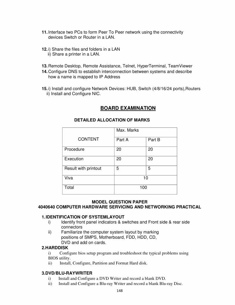
148
11. Interface two PCs to form Peer To Peer network using the connectivity
devices Switch or Router in a LAN.
12. i) Share the files and folders in a LAN ii) Share a printer in a LAN.
13. Remote Desktop, Remote Assistance, Telnet, HyperTerminal, TeamViewer
14. Configure DNS to establish interconnection between systems and describe
how a name is mapped to IP Address
15. i) Install and configure Network Devices: HUB, Switch (4/8/16/24 ports),Routers ii) Install and Configure NIC.
BOARD EXAMINATION
DETAILED ALLOCATION OF MARKS
CONTENT
Max. Marks
Part A Part B
Procedure 20 20
Execution 20 20
Result with printout 5 5
Viva 10
Total 100
MODEL QUESTION PAPER
4040640 COMPUTER HARDWARE SERVICING AND NETWORKING PRACTICAL
1. IDENTIFICATION OF SYSTEMLAYOUT i) Identify front panel indicators & switches and Front side & rear side
connectors ii) Familiarize the computer system layout by marking
positions of SMPS, Motherboard, FDD, HDD, CD,
DVD and add on cards.
2.HARDDISK
i) Configure bios setup program and troubleshoot the typical problems using
BIOS utility.
ii) Install, Configure, Partition and Format Hard disk.
3.DVD/BLU-RAYWRITER
i) Install and Configure a DVD Writer and record a blank DVD.
ii) Install and Configure a Blu-ray Writer and record a blank Blu-ray Disc.
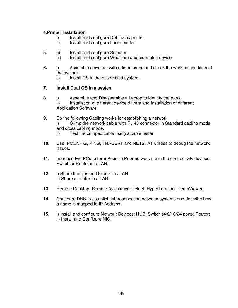
149
4.Printer Installation
i) Install and configure Dot matrix printer ii) Install and configure Laser printer
5. .i) Install and configure Scanner ii) Install and configure Web cam and bio-metric device
6. i) Assemble a system with add on cards and check the working condition of
the system. ii) Install OS in the assembled system.
7. Install Dual OS in a system
8. i) Assemble and Disassemble a Laptop to identify the parts.
ii) Installation of different device drivers and Installation of different Application Software.
9. Do the following Cabling works for establishing a network
i) Crimp the network cable with RJ 45 connector in Standard cabling mode and cross cabling mode. ii) Test the crimped cable using a cable tester.
10. Use IPCONFIG, PING, TRACERT and NETSTAT utilities to debug the network
issues.
11. Interface two PCs to form Peer To Peer network using the connectivity devices Switch or Router in a LAN.
12. i) Share the files and folders in aLAN
ii) Share a printer in a LAN.
13. Remote Desktop, Remote Assistance, Telnet, HyperTerminal, TeamViewer. 14. Configure DNS to establish interconnection between systems and describe how
a name is mapped to IP Address
15. i) Install and configure Network Devices: HUB, Switch (4/8/16/24 ports),Routers ii) Install and Configure NIC.
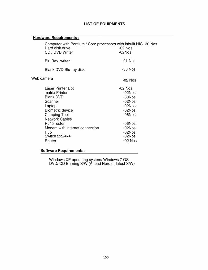
150
LIST OF EQUIPMENTS
Hardware Requirements :
Computer with Pentium / Core processors with inbuilt NIC -30 Nos Hard disk drive -02 Nos CD / DVD Writer Blu Ray writer Blank DVD,Blu-ray disk
-02Nos -01 No -30 Nos
Web camera -02 Nos Laser Printer Dot -02 Nos matrix Printer Blank DVD
-02Nos -30Nos
Scanner -02Nos Laptop -02Nos Biometric device -02Nos Crimping Tool -06Nos Network Cables RJ45Tester -06Nos Modem with internet connection -02Nos Hub -02Nos Switch 2x2/4x4 -02Nos
Router -02 Nos
Software Requirements:
Windows XP operating system/ Windows 7 OS DVD/ CD Burning S/W (Ahead Nero or latest S/W)
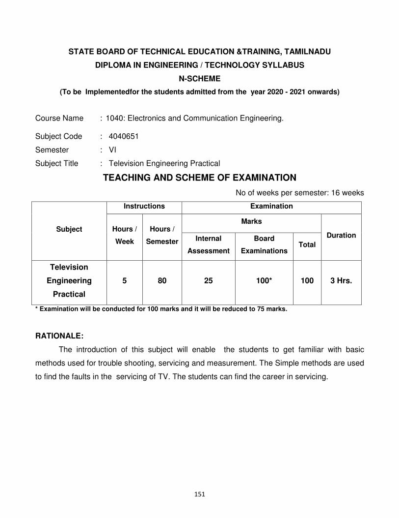
151
STATE BOARD OF TECHNICAL EDUCATION &TRAINING, TAMILNADU
DIPLOMA IN ENGINEERING / TECHNOLOGY SYLLABUS
N-SCHEME
(To be Implementedfor the students admitted from the year 2020 - 2021 onwards)
Course Name : 1040: Electronics and Communication Engineering. Subject Code : 4040651
Semester : VI
Subject Title : Television Engineering Practical
TEACHING AND SCHEME OF EXAMINATION
No of weeks per semester: 16 weeks
Subject
Instructions Examination
Hours /
Week
Hours /
Semester
Marks
Duration Internal
Assessment
Board
Examinations Total
Television
Engineering
Practical
5 80 25 100* 100 3 Hrs.
* Examination will be conducted for 100 marks and it will be reduced to 75 marks.
RATIONALE:
The introduction of this subject will enable the students to get familiar with basic
methods used for trouble shooting, servicing and measurement. The Simple methods are used
to find the faults in the servicing of TV. The students can find the career in servicing.
152
OBJECTIVES:
The students are able to
-> Understand the assembling of Antenna.
-> Construct and test the deflection circuits.
-> Construct and test the sync circuits.
->Service TV remote.
-> Check faults in power supply.
-> Find the faults in video section and audio section
-> Understand about DTH connection
-> Study the use of set of box
-> Service the monitors.
.4040651 TELEVISION ENGINEERING PRACTICAL
DETAILED SYLLABUS
Contents:Practical
Exercises
1.Assembling of yagiuda antenna.
2.Construct and test the sync separator circuit.
3.Construct a horizontal sawtooth generator and measure its frequency .
4.Construct a vertical sawtooth generator and measure its frequency.
5.Trouble shooting of IR TV Remote control unit.
6. Fault finding in SMPS and measure its different voltage levels.
7.Trouble shooting of EHT section in TV.
8.Trouble shooting of sound section in TV.
9.Study of RF Tuner.
10.Trouble shooting of deflection yoke with controls.
11.Servicing of computer monitors (observe the VGA signals using CRO)
12.Servicing of LED /LCD monitors.
13.Measure the dc voltages at various points in TV receiver .
153
BOARD EXAMINATION
Note: All the experiments to be kept for the examination.
DETAILED ALLOCATION OF MARKS
Circuit Diagram : 25 marks
Connection / Procedure : 25 marks
Execution and handling of equipment : 30 marks
Output / Result : 10 marks
Viva : 10 marks
TOTAL : 100 marks
MODEL QUESTION PAPER
4040651 TELEVISION ENGINEERING PRACTICAL
1.Construct a vertical sawtooth generator for the frequency of 50 hz and verify its output.
2.Troubleshoot the sound section in TV receiver and observe the values.
3.Troubleshoot the deflection yoke of TV receiver and draw the observed waveforms.
4.Troubleshoot the EHT section of TV receiver and measure the values.
5. Construct and test the sync separator circuit and observe the waveforms and draw.
6. Assemble the Yagi-uda antenna with the given antenna elements.
7. Service the given computer monitor and observe the VGA signals using CRO.
8 . Service the TV remote and find the fault.
9. Troubleshoot the given LED / LCD monitor and find the faults.
10. Service the given SMPS and measure the voltage levels.
11. Construct the horizontal sawtooth generator for the frequency of 15,625 hz and verify its
output.
12. Measure and write down the Voltage levels of the TV receiver given for troubleshooting .
13. Study the given RF tuner and explain the function of sections of RF tuner.
154
LIST OF EQUIPMENTS
1. Antenna elements ( dipole , reflector, director ) - 2 Sets.
2. Audio oscillator -5 Nos.
3. CRO – 2 Nos.
4. Power Supply ( 0 – 30v) – 5 Nos.
5. Multi meters-5.
6. SMPS-4 Nos.
7. IR TV remote receivers – 2 Nos.
8. B/W Television Receiver Trainer kit.
9. Color TV Receiver Trainer kit.
10. VGA Monitors- 2 Nos.
11. LCD / LED monitors -2 Nos.
155
STATE BOARD OF TECHNICAL EDUCATION &TRAINING, TAMILNADU
DIPLOMA IN ENGINEERING / TECHNOLOGY SYLLABUS
N-SCHEME
(To be Implementedfor the students admitted from the year 2020 - 2021 onwards)
Course Name : 1040:Electronics and Communication Engineering
Subject code : 4040652 Semester : VI
Subject title : MOBILE AND OPTICAL COMMUNICATION PRACTICAL
TEACHINGAND SCHEME OFEXAMINATION
No.ofweeks/ Semester: 16weeks
Subject
Instruction Examination
Hours
/week
Hours
/semester
Marks Duration
Internal Assessment
Board Examination
Total
Mobile and Optical Communication
Practical
5
80
25
100*
100
3 Hours
* Examination will be conducted for 100 marks and it will be reduced to 75 marks.
RATIONALE:
All types of Mobile Communication circuits are merged with Optical fiber links to get
Broad band services to Home and all working environments. Hence in this subject
Mobile Communication and Optical Communication related practical circuits are going
to be tested by the students. By Practicing the following experiments the students can
develop their skill which could be helpful for their self employment in future.
OBJECTIVES:
On completion ofthefollowing experiments, the students must be able to
� Understand the concept of Mobile Communication
� Know the working principle of Mobile Networks
� Know the working of Transmitter and Receiver in GSM
156
� Study the workingofSIMcardinGSMhandset and SIM card detection.
� StudyandobserveTransmitted/ReceivedRFsignal.
� StudyandobserveTransmitted(I&Q)/Received(I&Q)signalsconstellations.
� StudyandanalyzetheBuzzerin4GLTESmartPhoneTechBook.
� StudyandAnalyzetheVibratorin4GLTESmartphoneTechBook
� StudyofswitchfaultsinUserInterface Sectionof4GLTESmart Phone TechBook
� Studyandanalyzethe PowerManagementUnitin4GLTESmart PhoneTechBook
� Generate the Pseudo random binary sequence
� Test the VI characteristics of LED (Light emitter) and Photo diode (Light detector)
� Test the VI Characteristics of anOpto - coupler
� Test the performance of Time Division Multiple Access in Fiber optical
communication link
� Determine the Numerical aperture of the given optical fiber
4040652 MOBILE AND OPTICAL COMMUNICATION PRACTICAL
DETAILED SYLLABUS Contents: Practical
Exercises
MOBILE COMMUNICATION
(TounderstandtheBasiccircuitofMobilephone(Transmitter,
ReceiverandBasebandcontrolSection).
1. Tostudy the workingofSIMcardinGSMhandset and SIM card detection.
2. ToStudyandobserveTransmitted/ReceivedRFsignal.
3. StudyandobserveTransmitted(I&Q)/Received(I&Q)signalsconstellations.
4. StudyandanalyzetheBuzzerin4GLTESmartPhoneTechBook.
5. TostudyandAnalyzetheVibratorin4GLTESmartphoneTechBook
6. StudyofswitchfaultsinUserInterface Sectionof4GLTESmart Phone TechBook
7. Studyandanalyzethe PowerManagementUnitin4GLTESmart PhoneTechBook
8. Generation of Pseudo random binary sequence
OPTICAL COMMUNICATION
9. Construct a circuit to test the VI characteristics of LED (Light emitter) and Photo diode
157
(Light detector)
10. Construct a circuit to test the VI Characteristics of anOpto - coupler
11. Test the performance of Time Division Multiple Access in Fiber optical communication
link
12. Determine the Numerical aperture of the given optical fiber
BOARD EXAMINATION
DETAILED ALLOCATION OF MARKS
CIRCUIT DIAGRAM : 25 CONNECTION :
25
EXECUTION & HANDLING OF EQUIPMENT :
25
OUTPUT / RESULT :
15
VIVA – VOCE :
10
TOTAL : 100
MODEL QUESTION PAPER
4040652 MOBILE AND OPTICAL COMMUNIICATION PRACTICAL
1. Studythe workingofSIMcardinGSMhandset and SIM card detection.
2. StudyandobserveTransmitted/ReceivedRFsignal.
3. StudyandobserveTransmitted(I&Q)/Received(I&Q)signalsconstellations.
4. StudyandanalyzetheBuzzerin4GLTESmartPhoneTechBook.
5. StudyandAnalyzetheVibratorin4GLTESmartphoneTechBook
6. StudyofswitchfaultsinUserInterface Sectionof4GLTESmart Phone TechBook
7. Studyandanalyzethe PowerManagementUnitin4GLTESmart PhoneTechBook
8. Generate Pseudo random binary sequence
9. Construct a circuit to test the VI characteristics of LED (Light emitter) and Photo diode
(Light detector)
158
10. Construct a circuit to test the VI Characteristics of anOpto - coupler
11. Test the performance of Time Division Multiple Access in Fiber optical communication
link
12. Determine the Numerical aperture of the given optical fiber
LIST OF EQUIPMENTS
S.NO Name of the Equipment Range Required No.
1. Regulated Power Supply 0 – 30V 2
2. Dual trace CRO 60 MHz 5
3. Signal Generator - 5
4. Desk Top Computer - 2
5. Smart phone Techbook - 3
6. Digital Trainer Kit -. 2
7. Digital Multimeter - 5
159
STATE BOARD OF TECHNICAL EDUCATION &TRAINING, TAMILNADU
DIPLOMA IN ENGINEERING / TECHNOLOGY SYLLABUS
N-SCHEME
(To be Implementedfor the students admitted from the year 2020 - 2021 onwards)
Course Name : 1040:Electronics and Communication Engineering Subject Code : 4040653
Semester : VI
Subject Title : Embedded Systems Practical
TEACHING AND SCHEME OF EXAMINATION
No of weeks per semester: 16 weeks
Subject
Instructions Examination
Hours /
Week
Hours /
Semester
Marks
Duration Internal
Assessment
Board
Examinations Total
Embedded
Systems Practical 5 80 25 100* 100 3 Hrs.
* Examination will be conducted for 100 marks and it will be reduced to 75 marks.
RATIONALE:
The introduction of this subject will enable the students to have hands on experience in
using ARM Based trainer kit. The students are exposed to use the on chip peripherals using
embedded C language. They can also get familiar with the use of ARM instruction set. They
are learning the different methods for providing time delay and u se of serial communication.
32 bit ARM is a RISC processor which makes the students to expose to the new dimension in
the field of embedded systems.
160
OBJECTIVES:
The students are able to
-> Understand the use of instruction set by writing simple ARM ALP and simulate to see
output.
-> Know the application details of on chip peripherals.
-> familiarize with the register map of on chip Timer / counter.
-> Know the use of serial communication concepts using on chip UART0.
-> understand the use of GPIO and the connection of peripheral devices using these on
chip GPIO programmable port Pins.
-> Use the interrupts with the help of VIC.
-> Get used with pin connect block registers for programming the GPIO port pins.
-> interface stepper motor and its operation.
-> understand the multiplexing of seven segment LED display device.
.
161
4040653 EMBEDDED SYSTEMS PRACTICAL
DETAILED SYLLABUS
Contents:Practical
Exercises
1. Study of ARM Processor kit.(Example LPC 2148 kit)
2. Write assembly language program for addition, subtraction and multiplication and
simulate.
3. Write and execute C program to blink the LEDs using software delay routine.
4. Write and execute C program to blink the LEDs using on chip TIMER//
COUNTER for the delay(Using Polling method).
5. Write and execute C program to blink the LEDs using on chip TIMER//
COUNTER for the delay(Using interrupt method).
6. Write and execute C program to read the switch and display in the LEDs.
7. Write and execute C program to count external interrupt pulses EINTx (using VIC)
and Show the binary count value in LEDs.
8. Write and execute C program to display a number in seven segment LED .
9. Write and execute C program for serial transmission and reception using on chip
UART. Send the received character back to the PC by Polling method.
10. Write and execute C program for serial transmission and reception using on chip
UART. Send the received character back to the PC by Interrupt method.
11.Write and execute C program for accessing an internal ADC and display the
binary output in LEDs.
12. Write and execute C program to generate square wave using on chip DAC.
BOARD EXAMINATION Note:
1.Manual for the ARM instruction sets and manual for the trainer kit (Excluding
sample program) can be allowed for their board exam.
2.Definition for built in function for the board can be given to students for their
board function.
3.manual containing procedure for program down loading through boot loader
or JTAG can be given to students for their board exam.
4.Bit details of Registers of on chip peripheral devices can be given for the
board practical examination.
162
DETAILED ALLOCATION OF MARKS
I. Algorithm or Flow chart : 20 marks
II. Program : 30 marks
III. Execution : 30 marks
IV. Result : 10 marks
V. Viva : 10 marks
TOTAL : 100 marks
MODEL QUESTION PAPER
4040653 EMBEDDED SYSTEMS PRACTICAL
1.Write a C program to blink a LED with the time delay of 1 second .Time delay can
be generated using software delay routine.
2.Write a C program to blink the LEDS with the time delay. Generate the time delay
using internal TIMER in polling method and verify.
3.Write a C program to display the following single digit number ------- at seven
segment LED device.
4.Write a C program using on chip UART for serial transmission and reception
using polling method and check the output .
5.Write an assembly language program to add / subtract 32 bit numbers and
simulate the output result.
6. Write a C program to blink the LEDS with the time delay. Generate the time delay
using internal TIMER in interrupt method and verify.
7. Write a C program using on chip UART for serial transmission and reception
using interrupt method and verify the output.
8.Write a C program to convert analog signal to digital using internal ADC and verify
the binary output at the LEDs.
9.Write a C program to use the internal DAC to generate a square wave output and
observe the output at CRO.
10.Write a C program to get the input from a switch and display at the LEDs.
11.Write a C program to demonstrate the use of external interrupt using on chip VIC
and observe the result at the LEDs.
12.Write an assembly language program to multiply two numbers and simulate the
output result.
163
LIST OF EQUIPMENTS
1.ARM7 TDMI KIT – 15 numbers with interface boards for the above experiments
.The chip set may be TMS4701,LPC2138,LPC2148 or STR7 etc.
2.Desktop computer / Laptop -15 Nos
3.Interfaces :Seven segment display. LEDS ,switches and stepper motor .
4. Manual for the trainer kit and Interfaces.
5.Manual for the built in function for the board.
6.Bit details of registers of on chip peripherals.
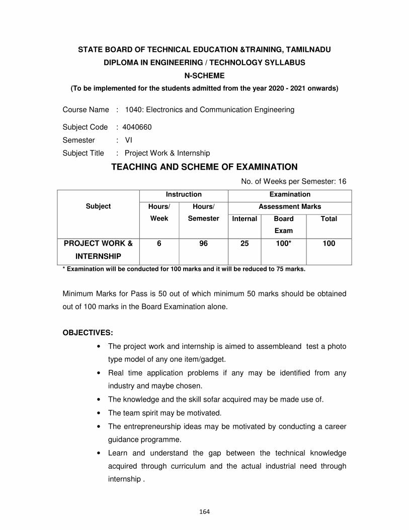
164
STATE BOARD OF TECHNICAL EDUCATION &TRAINING, TAMILNADU
DIPLOMA IN ENGINEERING / TECHNOLOGY SYLLABUS
N-SCHEME
(To be implemented for the students admitted from the year 2020 - 2021 onwards)
Course Name : 1040: Electronics and Communication Engineering Subject Code : 4040660
Semester : VI
Subject Title : Project Work & Internship
TEACHING AND SCHEME OF EXAMINATION
No. of Weeks per Semester: 16
Subject
Instruction Examination
Hours/
Week
Hours/
Semester
Assessment Marks
Internal Board
Exam
Total
PROJECT WORK &
INTERNSHIP
6 96 25 100* 100
* Examination will be conducted for 100 marks and it will be reduced to 75 marks.
Minimum Marks for Pass is 50 out of which minimum 50 marks should be obtained
out of 100 marks in the Board Examination alone.
OBJECTIVES:
• The project work and internship is aimed to assembleand test a photo
type model of any one item/gadget.
• Real time application problems if any may be identified from any
industry and maybe chosen.
• The knowledge and the skill sofar acquired may be made use of.
• The team spirit may be motivated.
• The entrepreneurship ideas may be motivated by conducting a career
guidance programme.
• Learn and understand the gap between the technical knowledge
acquired through curriculum and the actual industrial need through
internship .
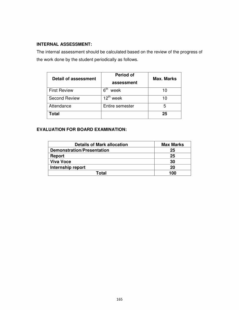
165
INTERNAL ASSESSMENT:
The internal assessment should be calculated based on the review of the progress of
the work done by the student periodically as follows.
Detail of assessment Period of
assessment Max. Marks
First Review 6th week 10
Second Review 12th week 10
Attendance Entire semester 5
Total 25
EVALUATION FOR BOARD EXAMINATION:
Details of Mark allocation Max Marks
Demonstration/Presentation 25
Report 25
Viva Voce 30
Internship report 20
Total 100