Embed Size (px)
Citation preview

ITEM CONTENTS UNIT LCD Type TFT/Transmissive/Normally white /
Size 4.3 Inch
Viewing Direction 12:00 (without image inversion) O’ Clock
Gray Scale Inversion Direction 6:00 O’ Clock
LCM (W × H × D) 106.30 × 68.00 × 8.70 mm3
Active Area (W × H) 95.04 × 53.86 mm2
Dot Pitch (W × H) 0.066 × 0.198 mm2
Number of Dots 480 (RGB) × 272 /
Driver IC SSD1963 + FT5446 /
Backlight Type 10 LEDs /
Surface Luminance 500 cd/m2
Interface Type Parallel 8/16b (i80 by default) /
Color Depth 16.7M /
Pixel Arrangement RGB Vertical Stripe /
Surface Treatment Anti-glare
Input Voltage 3.3 V
With/Without TSP Projected Capacitive Touch Panel /
Weight 91 g
LCD TFT Datasheet
RVT4.3A480272CFWC36
Rev.3.0.0
2018-04-11
LC
D T
FT
Mo
du
le S
pe
cif
ica
tio
n
Note 1: RoHS compliant
Note 2: LCM weight tolerance: ± 5%.
© 2014 Riverdi Page 2 of 21 www.riverdi.com
RVT4.3A480272CFWC36
LCD TFT Datasheet Rev.3.0.0
REVISION RECORD REVNO. REVDATE CONTENTS REMARKS
1.0 2014-11-12 Initial Release
1.1 2014-11-26 Update mechanical drawing
1.2 2014-12-19 Update interface description table
1.3 2015-01-19 Update LED lifetime
1.4 2015-02-24 Update thickness information
1.5 2015-06-15 Update surface treatment
1.6 2015-08-27 Adding Pin numbering in the mechanical drawing
1.7 2016-02-02 Update TP dimensions and total thickness
1.8 2016-08-12 Added inspection standards
1.9 2016-08-18 Updated dimension in drawing
1.10 2016-08-22 Update total thickness
2.0.0 2017-05-30 Glass change, new TFT open dimension, FFC shape, new TFT IC controller
2.1.0 2017-11-21 Updated electrical characteristics
3.0.0 2018-04-11 New CTP controller IC.

© 2014 Riverdi Page 3 of 21 www.riverdi.com
RVT4.3A480272CFWC36
LCD TFT Datasheet Rev.3.0.0
CONTENTS
REVISION RECORD ................................................................................................................................... 2
CONTENTS ............................................................................................................................................... 3
1 MODULE CLASSIFICATION INFORMATION ...................................................................................... 4
2 MODULE DRAWING ........................................................................................................................ 4
3 ABSOLUTE MAXIMUM RATINGS ...................................................................................................... 5
4 ELECTRICAL CHARACTERISTICS ........................................................................................................ 5
5 ELECTRO-OPTICAL CHARACTERISTICS ............................................................................................. 5
6 INTERFACE DESCRIPTION ................................................................................................................ 7
7 INTERFACE TIMING CHARACTERISTICS............................................................................................ 8
7.1 8080 Mode .............................................................................................................................. 8
7.2 Pixel Data Format .................................................................................................................... 8
7.3 Parallel 8080-series Interface Timing ...................................................................................... 9
8 LCD TIMING CHARACTERISTICS ..................................................................................................... 10
8.1 Clock and data input time diagram ....................................................................................... 10
8.2 Parallel RGB input timing table ............................................................................................. 10
9 CAPACITIVE TOUCH SCREEN PANEL SPECIFICATIONS ................................................................... 11
9.1 Mechanical characteristics .................................................................................................... 11
9.2 Electrical characteristics ........................................................................................................ 11
9.3 Interface timing characteristics ............................................................................................. 11
9.4 I2C Read/Write Interface Description ................................................................................... 12
9.5 Communication of the I2C interface with Host ..................................................................... 12
9.6 Touch data read protocol ...................................................................................................... 13
9.7 Data description. ................................................................................................................... 13
9.8 Interrupt Trigger Mode ......................................................................................................... 15
10 INSPECTION ............................................................................................................................... 16
10.1 Inspection condition .............................................................................................................. 16
10.2 Inspection standard ............................................................................................................... 17
11 RELIABILITY TEST ....................................................................................................................... 19
12 LEGAL INFORMATION ................................................................................................................ 20
© 2014 Riverdi Page 4 of 21 www.riverdi.com
RVT4.3A480272CFWC36
LCD TFT Datasheet Rev.3.0.0
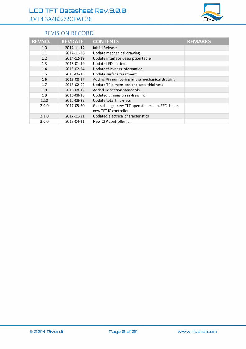
1 MODULE CLASSIFICATION INFORMATION
RV T 4.3 A 480272 C F W C 36
1. 2. 3. 4. 5. 6. 7. 8. 9. 10.
1. BRAND RV – Riverdi
2. PRODUCT TYPE T – TFT Standard
F – TFT Custom
3. DISPLAY SIZE
3.5 – 3.5”
4.3 – 4.3”
5.7 – 5.7”
7.0 – 7.0”
4. MODEL SERIAL NO. A (A-Z)
5. RESOLUTION
320240 – 320x240 px
480272 – 480x272 px
800480 – 800x480 px
6. INTERFACE
T – TFT LCD, RGB
L – TFT LCD, LVDS
C – TFT + Controller
7. FRAME N – No Frame
F – Mounting Frame
8. BACKLIGHT TYPE W – LED White
9. TOUCH PANEL
N – No Touch Panel
R – Resistive Touch Panel
C – Capacitive Touch Panel
10. VERSION 36 (00-99)
LCD TFT Datasheet Rev.3.0.0 RVT4.3A480272CFWC36
© 2014 Riverdi Page 4 of 21 www.riverdi.com
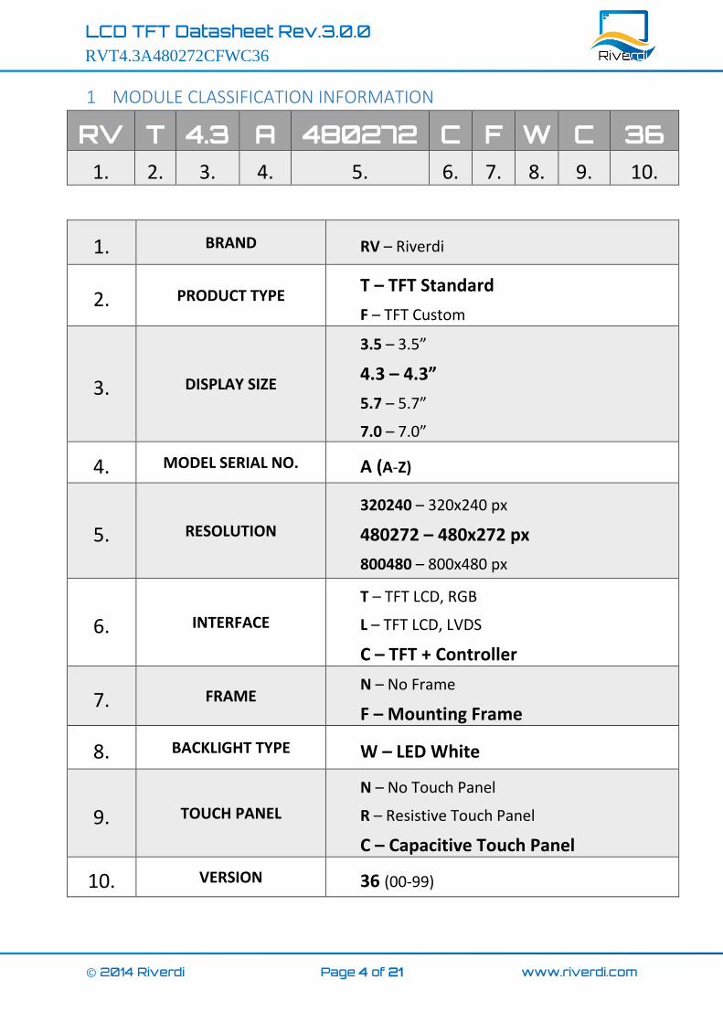
2 MODULE DRAWING

© 2014 Riverdi Page 5 of 21 www.riverdi.com
RVT4.3A480272CFWC36
LCD TFT Datasheet Rev.3.0.0
3 ABSOLUTE MAXIMUM RATINGS PARAMETER SYMBOL MIN MAX UNIT Supply Voltage for Logic VDD -0.3 4.6 V
Input Voltage for Logic VIN -0.3 VDD V
Input Voltage for LED Inverter BLVDD -0.3 7.0 V
Operating Temperature TOP -20 70 °C
Storage Temperature TST -30 80 °C
Humidity RH - 90% (Max 60°C) RH
4 ELECTRICAL CHARACTERISTICS PARAMETER SYMBOL MIN TYP MAX UNIT NOTES Supply Voltage for Module VDD 3.0 3.3 3.6 V
Input Voltage for LED Inverter BLVDD 2.8 3.3 5.5 V
Input Voltage ‘H’ level for BL_E pin BL_EH 1.5 - 5.5 V
Input Voltage ‘L’ level for BL_E pin BL_EL 0 - 0.7
Input Current (Exclude LED Backlight) IDD - 25 32 mA VDD = 3.3V
LED Backlight Current IDDbacklight 265 332 mA BLVDD=3.3V
LED Backlight Current IDDbacklight 156 195 mA BLVDD=5V
Total Input Current (Include LED Backlight 100%)
IDDtotal - 290 363 mA BLVDD=3.3V
Input Voltage ' H ' level VIH 0.7VDD - VDD V
Input Voltage ' L ' level VIL 0 - 0.2VDD V
LED Life Time - 30000 50000 - Hrs Note 1
Note 1: The LED life time is defined as the module brightness decrease to 50% original brightness at
Ta=25°C.
5 ELECTRO-OPTICAL CHARACTERISTICS ITEM SYMBOL CONDITION MIN TYP MAX UNIT REMARK NOTE Response Time Tr+Tf
θ=0° ∅=0°
Ta=25
- 20 30 ms Figure 1 4
Contrast Ratio Cr 320 400 - --- Figure 2 1
Luminance Uniformity
δ WHITE 80 - - % Figure 2 3
Surface Luminance Lv 440 550 - cd/m2 Figure 2 2
Viewing Angle Range
θ
∅ = 90° 35 50 - deg Figure 3
6
∅ = 270° 55 70 - deg Figure 3
∅ = 0° 55 70 - Deg Figure 3
∅ = 180° 55 70 - Deg Figure 3
CIE (x, y) Chromaticity
Red x
θ=0° ∅=0°
Ta=25
0.570 0.620 0.670
Figure 2
5
y 0.294 0.344 0.394
Green x 0.256 0.306 0.356
y 0.513 0.563 0.613
Blue x 0.083 0.133 0.183
y 0.099 0.149 0.199
White x 0.250 0.300 0.350
y 0.280 0.330 0.380

© 2014 Riverdi Page 6 of 21 www.riverdi.com
RVT4.3A480272CFWC36
LCD TFT Datasheet Rev.3.0.0
Note 1. Contrast Ratio(CR) is defined mathematically as below, for more information see Figure 1.
Contrast Ratio = Average Surface Luminance with all white pixels (P1, P2, P3, P4, P5)
Average Surface Luminance with all black pixels (P1, P2, P3, P4, P5)
Note 2. Surface luminance is the LCD surface from the surface with all pixels displaying white. For more
information see Figure 2.
Lv = Average Surface Luminance with all white pixels (P1, P2, P3, P4, P5)
Note 3. The uniformity in surface luminance δ WHITE is determined by measuring luminance at each
test position 1 through 5, and then dividing the maximum luminance of 5 points luminance by
minimum luminance of 5 points luminance. For more information see Figure 2.
δ WHITE = Minimum Surface Luminance with all white pixels (P1, P2, P3, P4, P5)
Maximum Surface Luminance with all white pixels (P1, P2, P3, P4, P5)
Note 4. Response time is the time required for the display to transition from white to black (Rise Time,
Tr) and from black to white (Decay Time, Tf). For additional information see FIG 1. The test equipment
is Autronic-Melchers’s ConoScope series.
Note 5. CIE (x, y) chromaticity, the x, y value is determined by measuring luminance at each test
position 1 through 5, and then make average value.
Note 6. Viewing angle is the angle at which the contrast ratio is greater than 2. For TFT module the
contrast ratio is greater than 10. The angles are determined for the horizontal or x axis and the vertical
or y axis with respect to the z axis which is normal to the LCD surface. For more information see Figure
3.
Note 7. For viewing angle and response time testing, the testing data is based on Autronic-Melchers’s
ConoScope series. Instruments for Contrast Ratio, Surface Luminance, Luminance Uniformity, CIE the
test data is based on TOPCON’s BM-5 photo detector.
Figure 1. The definition of response time

© 2014 Riverdi Page 7 of 21 www.riverdi.com
RVT4.3A480272CFWC36
LCD TFT Datasheet Rev.3.0.0
Figure 2. Measuring method for Contrast ratio, surface luminance, Luminance uniformity, CIE (x, y) chromaticity
Figure 3.The definition of viewing angle
6 INTERFACE DESCRIPTION PIN NO. SYMBOL I/O DESCRIPTION
1 GND P Power Ground
2 VDD P Power Supply: +3.3V
3 BL_E I Backlight Control Signal, H: On/L: Off (internally pulled-up to BLVDD)
4 D/C I Data/Command Select
5 WR I Write Strobe Signal
6 RD I Read Strobe Signal
7-22 D0-D15 I Data Bus. Pins not used should be floating.
23 NC - No Connection
24 TP_INT O Touch Panel INT
25 CS I Chip Select
26 RESET I Hardware reset
27 DISP ON I Display Control H: On/L: Off (internally pulled-up)
28 NC - No Connection
29 TP_SCL I/O Touch Panel I2C SCL Signal
30 TP_SDA I/O Touch Panel I2C SDA Signal
31 TP_RST I Touch Panel RST Signal, Active Low
32 NC - No Connection
33 BLGND P Backlight ground, can be connected to GND
34 BLGND P Backlight ground, can be connected to GND
35 BLVDD P Backlight power supply, can be connected to VDD
36 BLVDD P Backlight power supply, can be connected to VDD
© 2014 Riverdi Page 8 of 21 www.riverdi.com
RVT4.3A480272CFWC36
LCD TFT Datasheet Rev.3.0.0
7 INTERFACE TIMING CHARACTERISTICS
7.1 8080 Mode
The 8080 mode MCU interface consist of CS#, D/C#, RD#, WR#, D[15:0]. This interface uses WR# to define a write cycle and RD# for read cycle. If the WR# goes low when the CS# signal is low, the data or command will be latched into the system at the rising edge of WR#. Similarly, the read cycle will start when RD# goes low and end at the rising edge of RD#.
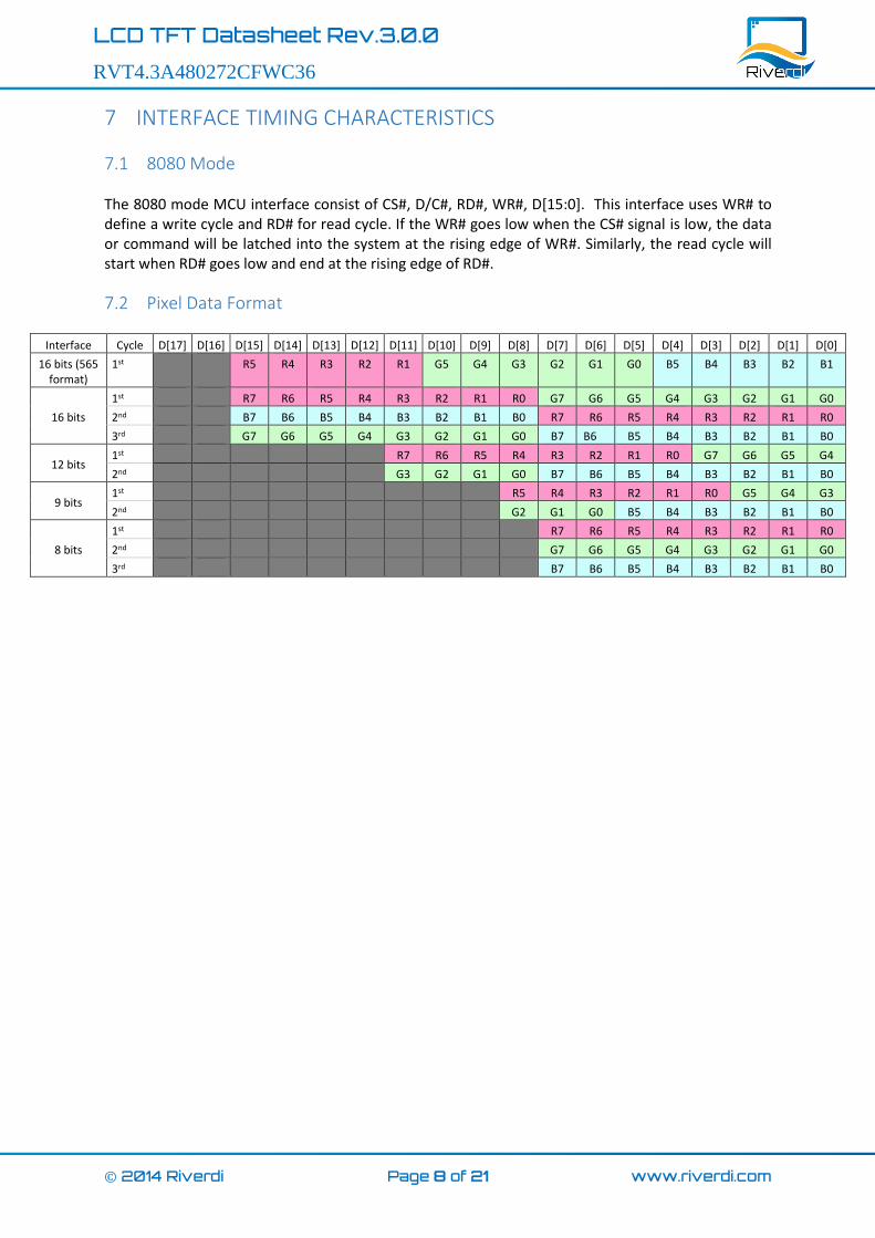
7.2 Pixel Data Format
Interface Cycle D[17] D[16] D[15] D[14] D[13] D[12] D[11] D[10] D[9] D[8] D[7] D[6] D[5] D[4] D[3] D[2] D[1] D[0]
16 bits (565 format)
1st R5 R4 R3 R2 R1 G5 G4 G3 G2 G1 G0 B5 B4 B3 B2 B1
16 bits
1st R7 R6 R5 R4 R3 R2 R1 R0 G7 G6 G5 G4 G3 G2 G1 G0
2nd B7 B6 B5 B4 B3 B2 B1 B0 R7 R6 R5 R4 R3 R2 R1 R0
3rd G7 G6 G5 G4 G3 G2 G1 G0 B7 B6 B5 B4 B3 B2 B1 B0
12 bits 1st
R7 R6 R5 R4 R3 R2 R1 R0 G7 G6 G5 G4
2nd
G3 G2 G1 G0 B7 B6 B5 B4 B3 B2 B1 B0
9 bits 1st
R5 R4 R3 R2 R1 R0 G5 G4 G3
2nd
G2 G1 G0 B5 B4 B3 B2 B1 B0
8 bits
1st
R7 R6 R5 R4 R3 R2 R1 R0
2nd
G7 G6 G5 G4 G3 G2 G1 G0
3rd
B7 B6 B5 B4 B3 B2 B1 B0

© 2014 Riverdi Page 9 of 21 www.riverdi.com
RVT4.3A480272CFWC36
LCD TFT Datasheet Rev.3.0.0
7.3 Parallel 8080-series Interface Timing
Figure 4. Parallel 8080-series Interface Timing Diagram (Write Cycle)
Figure 5.Parallel 8080-series Interface Timing Diagram (Read Cycle)

© 2014 Riverdi Page 10 of 21 www.riverdi.com
RVT4.3A480272CFWC36
LCD TFT Datasheet Rev.3.0.0
8 LCD TIMING CHARACTERISTICS
8.1 Clock and data input time diagram
Figure 6. Clock and data input time diagram
8.2 Parallel RGB input timing table
PARAMETER SYMBOL MIN TYP MAX UNIT DCLK Frequency Fclk 5 9 12 MHz
VSD Period Time Tv 277 288 400 H
VSD Display Area Tvd 272 H
VSD Back Porch Tvb 3 8 31 H
VSD Front Porch Tvfp 2 8 97 H
HSD Period Time Th 520 525 800 DCLK
HSD Display Area Thd 480 DCLK
HSD Back Porch Thbp 36 40 255 DCLK
HSD Front Porch Thfp 4 5 65 DCLK

© 2014 Riverdi Page 11 of 21 www.riverdi.com
RVT4.3A480272CFWC36
LCD TFT Datasheet Rev.3.0.0
9 CAPACITIVE TOUCH SCREEN PANEL SPECIFICATIONS
9.1 Mechanical characteristics
DESCRIPTION INL SPECIFICATION REMARK Touch Panel Size 4.3 inch
Outline Dimension (OD) 104.0mm x 65.4mm Cover Lens Outline
Product Thickness 1.7mm
Glass Thickness 0.7mm
Ink View Area 96.54mm x 55.36mm
Sensor Active Area 98.0mm x 56.5mm
Input Method 5 Finger
Activation Force Touch
Surface Hardness ≥7H
9.2 Electrical characteristics
DESCRIPTION SPECIFICATION Operating Voltage DC 2.8~3.3V
Power Consumption (IDD) Active Mode 10~18mA
Sleep Mode 30~50μA
Interface I2C
Linearity <1.5%
Controller FT5446
I2C address 0x38 (7 bit address)
Resolution 1280*768
9.3 Interface timing characteristics
PARAMETER MIN MAX UNIT SCL Frequency 0 400 kHz
Bus Free Time Between a STOP and START Condition 4.7 / μs
Hold Time (repeated) START Condition 4.0 / μs
Data Setup Time 250 / ns
Setup Time for Repeated START Condition 4.7 / μs
Setup Time for STOP Condition 4.0 / μs

© 2014 Riverdi Page 12 of 21 www.riverdi.com
RVT4.3A480272CFWC36
LCD TFT Datasheet Rev.3.0.0
9.4 I2C Read/Write Interface Description
Figure 7. Write N bytes to I2C slave
Figure 8. Set Data Address
Figure 9. Read X bytes from I2C Slave
9.5 Communication of the I2C interface with Host
Figure 10. Communication of the I2C interface with Host
© 2014 Riverdi Page 13 of 21 www.riverdi.com
RVT4.3A480272CFWC36
LCD TFT Datasheet Rev.3.0.0
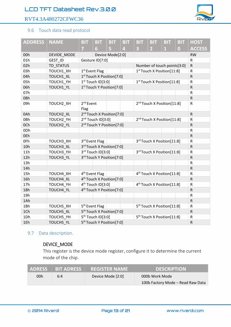
9.6 Touch data read protocol
ADDRESS NAME BIT7
BIT6
BIT5
BIT4
BIT3
BIT2
BIT1
BIT0
HOST ACCESS
00h DEVIDE_MODE Device Mode[2:0] RW
01h GEST_ID Gesture ID[7:0] R
02h TD_STATUS Number of touch points[3:0] R
03h TOUCH1_XH 1st Event Flag 1st Touch X Position[11:8] R
04h TOUCH1_XL 1st Touch X Position[7:0] R
05h TOUCH1_YH 1st Touch ID[3:0] 1st Touch X Position[11:8] R
06h TOUCH1_YL 1st Touch Y Position[7:0] R
07h R
08h R
09h TOUCH2_XH 2nd Event Flag
2nd Touch X Position[11:8] R
0Ah TOUCH2_XL 2nd Touch X Position[7:0] R
0Bh TOUCH2_YH 2nd Touch ID[3:0] 2nd Touch X Position[11:8] R
0Ch TOUCH2_YL 2nd Touch Y Position[7:0] R
0Dh R
0Eh R
0Fh TOUCH3_XH 3rd Event Flag 3rd Touch X Position[11:8] R
10h TOUCH3_XL 3rd Touch X Position[7:0] R
11h TOUCH3_YH 3rd Touch ID[3:0] 3rd Touch X Position[11:8] R
12h TOUCH3_YL 3rd Touch Y Position[7:0] R
13h R
14h R
15h TOUCH4_XH 4th Event Flag 4th Touch X Position[11:8] R
16h TOUCH4_XL 4th Touch X Position[7:0] R
17h TOUCH4_YH 4th Touch ID[3:0] 4th Touch X Position[11:8] R
18h TOUCH4_YL 4th Touch Y Position[7:0] R
19h R
1Ah R
1Bh TOUCH5_XH 5th Event Flag 5th Touch X Position[11:8] R
1Ch TOUCH5_XL 5th Touch X Position[7:0] R
1Dh TOUCH5_YH 5th Touch ID[3:0] 5th Touch X Position[11:8] R
1Eh TOUCH5_YL 5th Touch Y Position[7:0] R
9.7 Data description.
DEVICE_MODE
This register is the device mode register, configure it to determine the current
mode of the chip.
ADRESS BIT ADRESS REGISTER NAME DESCRIPTION
00h 6:4 Device Mode [2:0] 000b Work Mode
100b Factory Mode – Read Raw Data

© 2014 Riverdi Page 14 of 21 www.riverdi.com
RVT4.3A480272CFWC36
LCD TFT Datasheet Rev.3.0.0
GEST_ID
This register describes the gesture of a valid touch.
ADRESS BIT ADRESS REGISTER NAME DESCRIPTION
01h 7:0 Gesture ID [7:0] Gesture ID
0x10 Move Up
0x14 Move Down
0x18 Move Right
0x48 Zoom In
0x49 Zoom Out
0x00 No Gesture
TD_STATUS
This register is the Touch Data status register.
ADRESS BIT ADRESS REGISTER NAME DESCRIPTION
02h 3:0 Number of Touch Points [2:0]
How Many Points Detected
1-5 is Valid
7:4
TOUCHn_XH(n:1-10)
This register describes MSB of the X coordinate of the nth touch point and the
corresponding event flag.
ADRESS BIT ADRESS REGISTER NAME DESCRIPTION
03h
~
39h
7:6 Event Flag 00b: Put Down
01b: Put Up
10b: Contact
11b: Reserved
5:4 Reserved
3:0 Touch X Position [11:8] MSB of Touch X Position in Pixels
TOUCHn_XL(n:1-10)
This register describes LSB of the X coordinate of the nth touch point.
ADRESS BIT ADRESS REGISTER NAME DESCRIPTION
04h
~
3Ah
7:0 Touch X Position [7:0] LSB of the Touch X Position in Pixels

© 2014 Riverdi Page 15 of 21 www.riverdi.com
RVT4.3A480272CFWC36
LCD TFT Datasheet Rev.3.0.0
TOUCHn_YH(n:1-10)
This register describes MSB of the Y coordinate of the nth touch point and
corresponding touch ID.
ADRESS BIT ADRESS REGISTER NAME DESCRIPTION
05h
~
3Bh
7:4 Touch ID[3:0] Touch ID of Touch Point
3:0 Touch X Position [11:8] MSB of Touch Y Position in Pixels
TOUCHn_YL(n:1-10)
This register describes LSB of the Y coordinate of the nth touch point.
ADRESS BIT ADRESS REGISTER NAME DESCRIPTION
05h
~
3Bh
7:0 Touch X Position [7:0] LSB of the Touch Y Position in Pixels
9.8 Interrupt Trigger Mode
Figure 11. Interrupt trigger mode timing
© 2014 Riverdi Page 16 of 21 www.riverdi.com
RVT4.3A480272CFWC36
LCD TFT Datasheet Rev.3.0.0
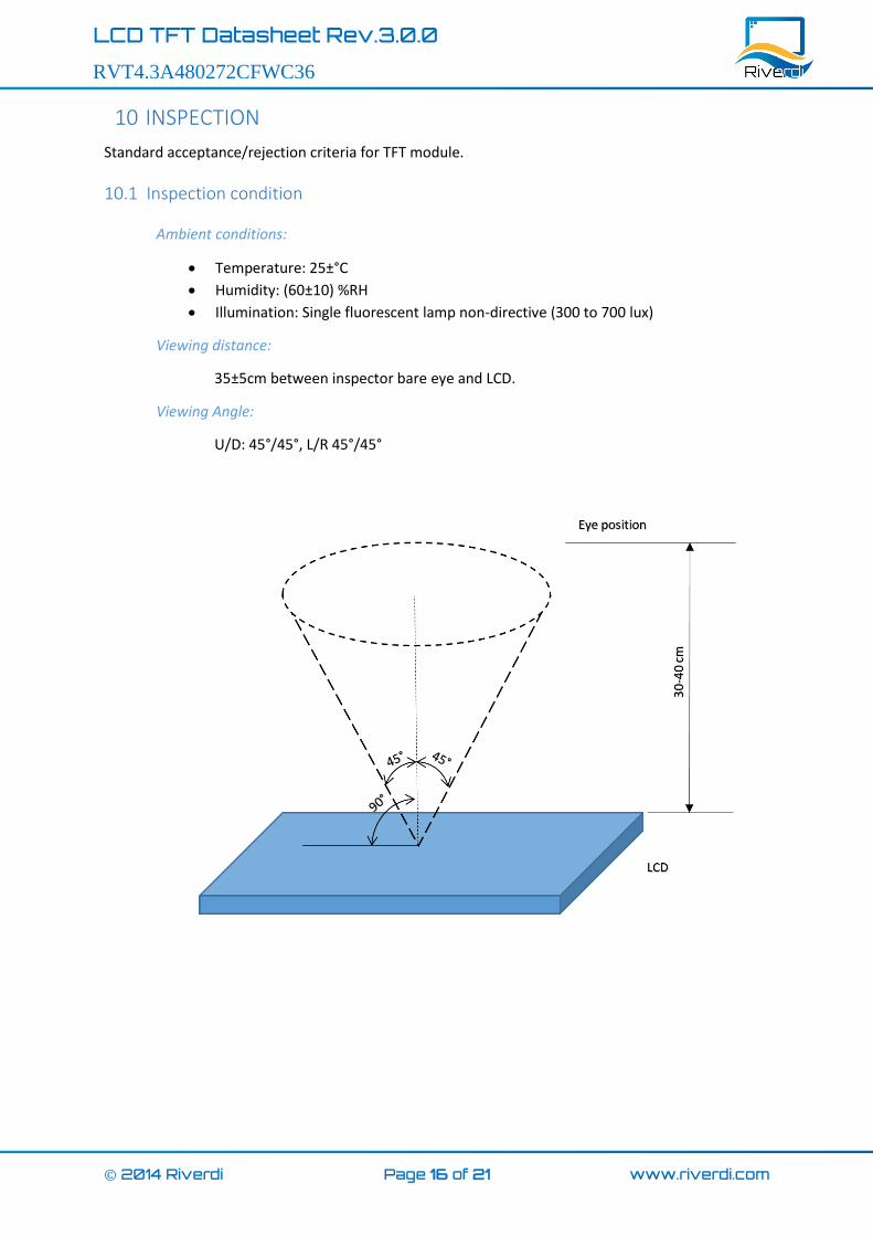
10 INSPECTION
Standard acceptance/rejection criteria for TFT module.
10.1 Inspection condition
Ambient conditions:
• Temperature: 25±°C
• Humidity: (60±10) %RH
• Illumination: Single fluorescent lamp non-directive (300 to 700 lux)
Viewing distance:
35±5cm between inspector bare eye and LCD.
Viewing Angle:
U/D: 45°/45°, L/R 45°/45°

© 2014 Riverdi Page 17 of 21 www.riverdi.com
RVT4.3A480272CFWC36
LCD TFT Datasheet Rev.3.0.0
10.2 Inspection standard
Item Criterion
Black spots, white spots, light leakage, Foreign Particle (round Type)
𝐷 =(𝑥 + 𝑦)
2
*Spots density: 10 mm2
Size < 5”
Average Diameter Qualified Qty
D < 0.2 mm Ignored
0.2 mm < D < 0.3 mm 3
0.3 mm < D < 0.5 mm 2
0.5 mm < D 0
Size >= 5”
Average Diameter Qualified Qty
D<0.2 mm Ignored
0.2 mm < D < 0.3 mm 4
0.3 mm < D < 0.5 mm 2
0.5 mm < D 0
LCD black spots, white spots, light leakage (line Type)
*Spots density: 10 mm2
Size < 5”
Length Width Qualified Qty
- W< 0.02 Ignored
L < 3.0 0.02 < W <0.05 2
L < 2.5 0.05 < W <0.08
- 0.08 < W 0
Size >= 5”
Length Width Qualified Qty
- W< 0.02 Ignored
L < 3.0 0.02 < W <0.05 4
L < 2.5 0.05 < W <0.08
- 0.08 < W 0

© 2014 Riverdi Page 18 of 21 www.riverdi.com
RVT4.3A480272CFWC36
LCD TFT Datasheet Rev.3.0.0
Item Criterion
Clear spots
Size >= 5”
Average Diameter Qualified Qty
D<0.2 mm Ignored
0.2 mm < D < 0.3 mm 4
0.3 mm < D < 0.5 mm 2
0.5 mm < D 0
*Spots density: 10 mm
Size < 5”
Average Diameter Qualified Qty
D < 0.2 mm Ignored
0.2 mm < D < 0.3 mm 3
0.3 mm < D < 0.5 mm 2
0.5 mm < D 0
Polarizer bubbles
Size < 5”
Average Diameter Qualified Qty
D < 0.2 mm Ignored
0.2 mm < D < 0.5 mm 3
0.5 mm < D < 1 mm 2
1 mm < D 0
Total Q’ty 3
Size >= 5”
Average Diameter Qualified Qty
D<0.25 mm Ignored
0.25 mm < D < 0.5 mm 3
0.5 mm < D 0
Electrical Dot Defect
Size < 5”
item Qualified Qty
Black do defect 4
Bright dot defect 2
Total Dot 5
Size >= 5”
item Qualified Qty
Black do defect 5
Bright dot defect 2
Total Dot 5

© 2014 Riverdi Page 19 of 21 www.riverdi.com
RVT4.3A480272CFWC36
LCD TFT Datasheet Rev.3.0.0
Item Criterion
Touch panel spot
Size < 5”
Average Diameter Qualified Qty
D < 0.2 mm Ignored
0.2 mm < D < 0.4 mm 5
0.4 mm < D < 0.5 mm 2
0.5 mm < D 0
Size >= 5”
Average Diameter Qualified Qty
D<0.25 mm Ignored
0.25 mm < D < 0.5 mm 4
0.5 mm < D 0
Touch panel White Line Scratch
Size < 5”
Length Width Qualified Qty
- W< 0.02 Ignored
L < 3.0 0.02 < W <0.05 2
L < 2.5 0.05 < W <0.08
- 0.08 < W 0
Size >= 5”
Length Width Qualified Qty
- W< 0.03 Ignored
L < 5.0 0.03 < W <0.05 2
- 0.05 < W 0
11 RELIABILITY TEST
NO. TEST ITEM TEST CONDITION 1 High Temperature Storage 80±2°C/240hours
2 Low Temperature Storage -30±2°C/240hours
3 High Temperature Operating 70±2°C/240hours
4 Low Temperature Operating -20±2°C/240hours
5 Temperature Cycle -30±2°C~25~80±2°C × 20 cycles (30min.) (5min.) (30min.)
6 Damp Proof Test 60°C ±5°C × 90%RH/240hours
7 Vibration Test Frequency 10Hz~55Hz Amplitude of vibration: 1.5mm Sweep: 10Hz~55Hz~10Hz X, Y, Z 2 hours for each direction.
8 Package Drop Test Height:60 cm 1 corner,3 edges,6 surfaces
9 ESD Test Air: ±4KV 150pF/330Ω 5 times Contact: ±2KV 150pF/330Ω 5 time

© 2014 Riverdi Page 20 of 21 www.riverdi.com
RVT4.3A480272CFWC36
LCD TFT Datasheet Rev.3.0.0
12 LEGAL INFORMATION
Riverdi makes no warranty, either expressed or implied with respect to any product, and specifically
disclaims all other warranties, including, without limitation, warranties for merchantability, non-
infringement and fitness for any particular purpose. Information about device are the property of Riverdi
and may be the subject of patents pending or granted. It is not allowed to copy or disclosed this document
without prior written permission.
Riverdi endeavors to ensure that the all contained information in this document are correct but does not
accept liability for any error or omission. Riverdi products are in developing process and published
information may be not up to date. Riverdi reserves the right to update and makes changes to Specifications
or written material without prior notice at any time. It is important to check the current position with
Riverdi.
Images and graphics used in this document are only for illustrative the purpose. All images and graphics are
possible to be displayed on the range products of Riverdi, however the quality may vary. Riverdi is no liable
to the buyer or to any third part for any indirect, incidental, special, consequential, punitive or exemplary
damages (including without limitation lost profits, lost savings, or loss of business opportunity) relating to
any product, service provided or to be provided by Riverdi, or the use or inability to use the same, even if
Riverdi has been advised of the possibility of such damages.
Riverdi products are not fault tolerant nor designed, manufactured or intended for use or resale as on line
control equipment in hazardous environments requiring fail – safe performance, such as in the operation
of nuclear facilities, aircraft navigation or communication systems, air traffic control, direct life support
machines or weapons systems in which the failure of the product could lead directly to death, personal
injury or severe physical or environmental damage (‘High Risk Activities’). Riverdi and its suppliers
specifically disclaim any expressed or implied warranty of fitness for High Risk Activities. Using Riverdi
products and devices in 'High Risk Activities' and in any other application is entirely at the buyer’s risk, and
the buyer agrees to defend, indemnify and hold harmless Riverdi from any and all damages, claims or
expenses resulting from such use. No licenses are conveyed, implicitly or otherwise, under any Riverdi
intellectual property rights.


![Zilla Panchayath Dharwad 4(1)a.pdf · +-lg: 7016-17 2016-17 22: 2016-17 2016-17 1:åeffi-25: 2016-17 2016-17 2016-17 2016-17 2016-17 2016 2016d 2016 08-08-2016 dad] 09 08-2016 09-08-2016](https://img.pdfslide.net/doc/110x75/5f4442908a716769256afc45/zilla-panchayath-41apdf-lg-7016-17-2016-17-22-2016-17-2016-17-1effi-25.jpg)