Embed Size (px)
Citation preview
1
ECOM 4311—Digital System Design with
VHDL
Course information
2
Course Description:
• This course Introduces the design of complex digital
systems using hardware description languages.
• Teaches design methodologies which partition a
system into a datapath and controller.
• Focuses on synthesizable RTL VHDL code for digital
circuit design using dataflow, structural, and
behavioral coding styles.
• Introduces VHDL simulation and verification, and
FPGA synthesis, placement, routing, timing analysis
and performance optimization.
3
Outcomes:
• Understand how to describe a digital system using a
Hardware Description Language (VHDL).
• Understand and use combinational logic circuits.
• Understand how Finite State Machines work, and
design them using VHDL
• Understand the HDL design flow.
• Understand how analog effects limit the performance
of digital systems.
• Simulate digital systems and prototype them on an
FPGA (upon availability).
4
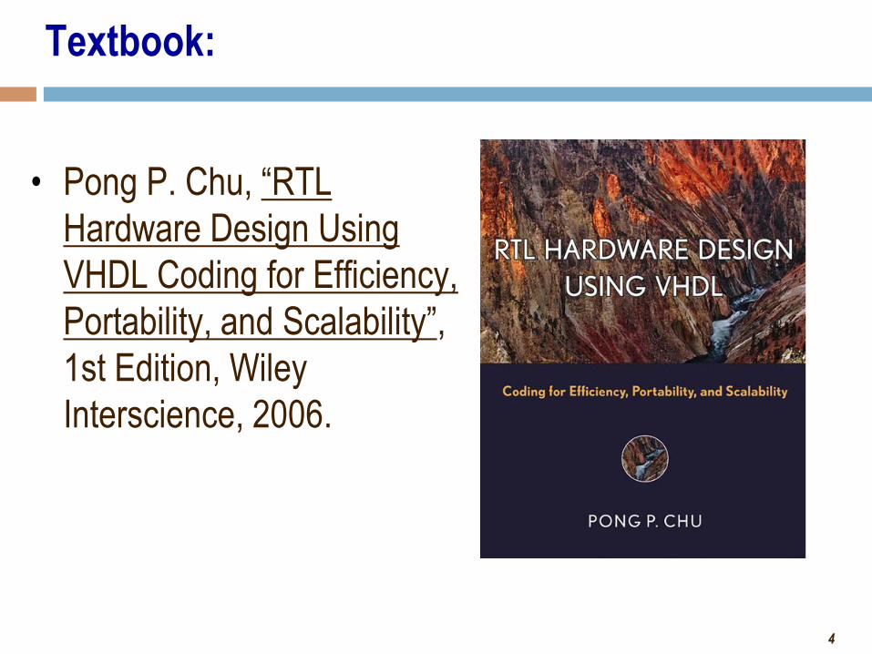
Textbook:
• Pong P. Chu, “RTL
Hardware Design Using
VHDL Coding for Efficiency,
Portability, and Scalability”,
1st Edition, Wiley
Interscience, 2006.
5
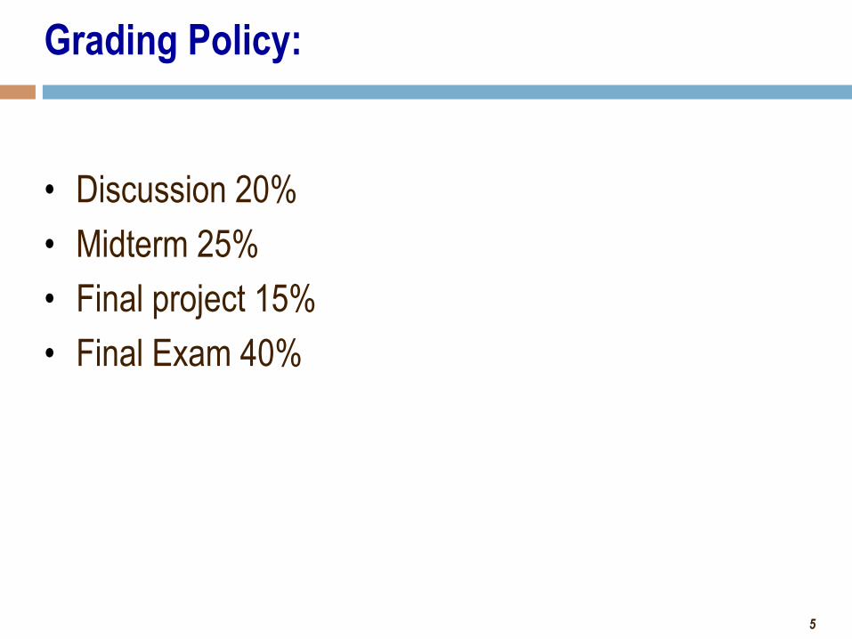
Grading Policy:
• Discussion 20%
• Midterm 25%
• Final project 15%
• Final Exam 40%

6
Introduction to
Digital System Design
ECOM 4311—Digital System Design with VHDL
7
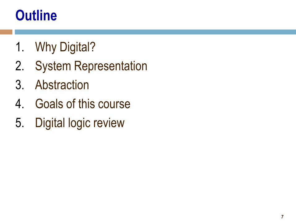
Outline
1. Why Digital?
2. System Representation
3. Abstraction
4. Goals of this course
5. Digital logic review
8
1. Why Digital
9
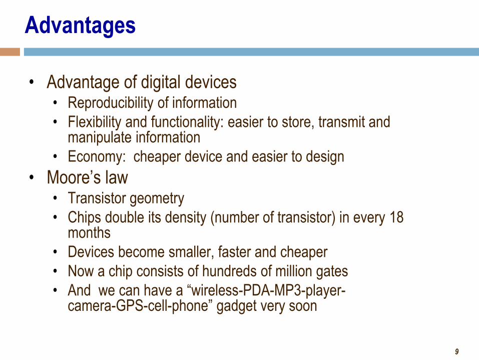
Advantages
• Advantage of digital devices • Reproducibility of information
• Flexibility and functionality: easier to store, transmit and manipulate information
• Economy: cheaper device and easier to design
• Moore’s law • Transistor geometry
• Chips double its density (number of transistor) in every 18 months
• Devices become smaller, faster and cheaper
• Now a chip consists of hundreds of million gates
• And we can have a “wireless-PDA-MP3-player- camera-GPS-cell-phone” gadget very soon
10
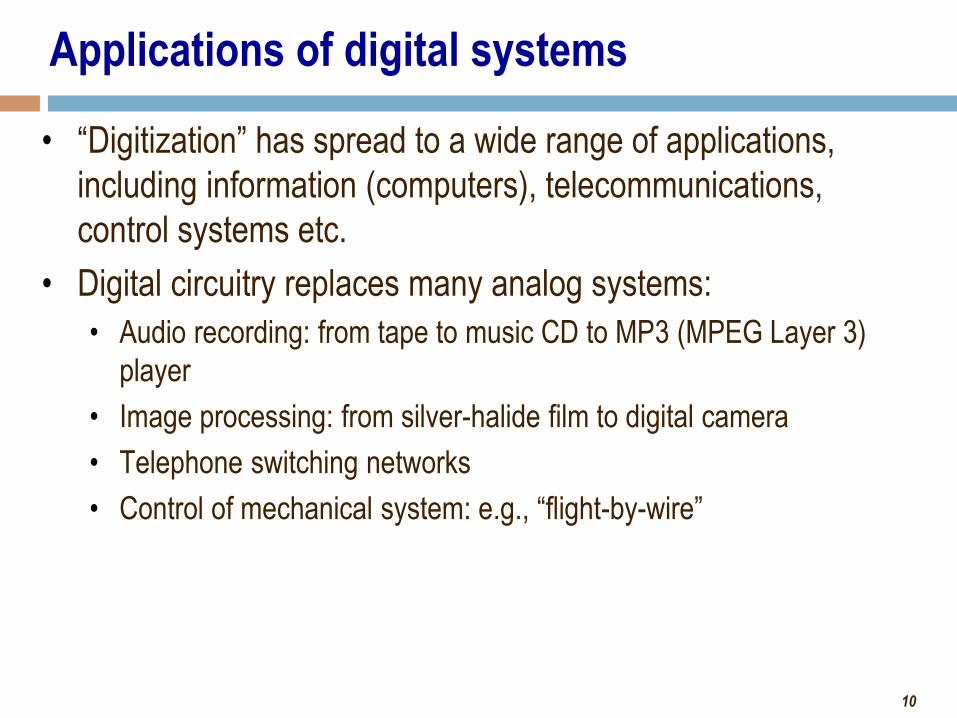
Applications of digital systems
• “Digitization” has spread to a wide range of applications,
including information (computers), telecommunications,
control systems etc.
• Digital circuitry replaces many analog systems:
• Audio recording: from tape to music CD to MP3 (MPEG Layer 3)
player
• Image processing: from silver-halide film to digital camera
• Telephone switching networks
• Control of mechanical system: e.g., “flight-by-wire”

11
2. System Representation
(View)
12
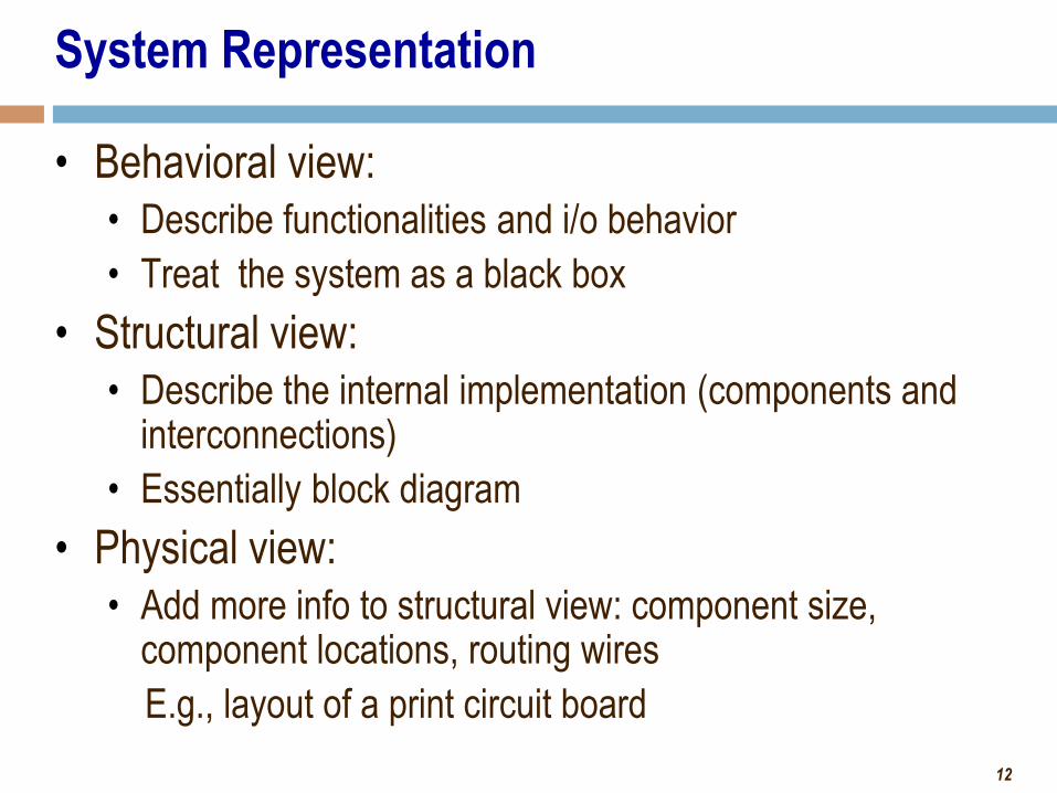
System Representation
• Behavioral view:
• Describe functionalities and i/o behavior
• Treat the system as a black box
• Structural view:
• Describe the internal implementation (components and interconnections)
• Essentially block diagram
• Physical view:
• Add more info to structural view: component size, component locations, routing wires
E.g., layout of a print circuit board

13
e.g., structural and physical view
14
3. Abstraction
15
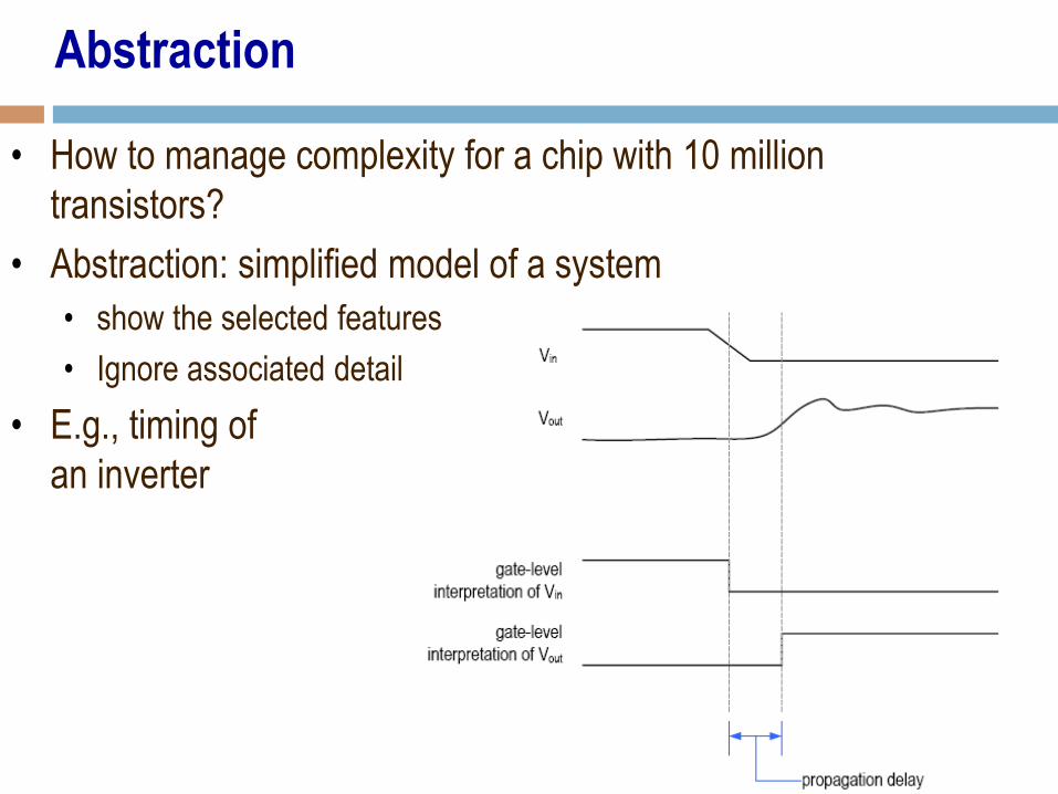
Abstraction
• How to manage complexity for a chip with 10 million
transistors?
• Abstraction: simplified model of a system
• show the selected features
• Ignore associated detail
• E.g., timing of
an inverter
16
• An abstraction is a simplified model of the system,
showing only the selected features and ignoring the
associated details.
• A high-level abstraction is focused and contains
only the most vital data.
• a low-level abstraction is more detailed and takes account of previously ignored information.
17
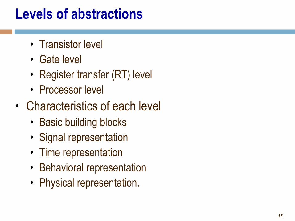
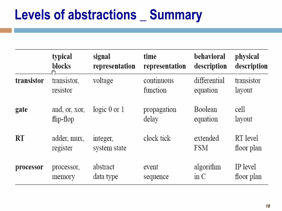
Levels of abstractions
• Transistor level
• Gate level
• Register transfer (RT) level
• Processor level
• Characteristics of each level
• Basic building blocks
• Signal representation
• Time representation
• Behavioral representation
• Physical representation.
18
Levels of abstractions _ Summary
19
Goal of this course
• Goal: • T learn how to systematically develop an efficient, portable RT-
level designs that can easily be integrated into a larger system.
• Design for efficiency
• Design for “large” Large module, large system, overall development process
• Design for portability Portability means that the same design description can be used
in different applications.
20
Digital Logic Review
21
Review – Combinational Logic
• Basic Logic Review • Basic Gates
• DeMorgan’s Law
• Combinational Logic Blocks • Multiplexers
• Decoders, Demultiplexers
• Encoders, Priority Encoders
• Half Adders, Full Adders
• Multi-Bit Combinational Logic Blocks • Multi-bit multiplexers
• Multi-bit adders
• Comparators
22
• Sequential Logic Building Blocks
• Latches, Flip-Flops
• Sequential Logic Circuits
• Registers, Shift Registers, Counters
• Memory (RAM, ROM)
Review – Sequential Logic

23
Basic Concepts
• Simple logic gates
• AND 0 if one or more inputs is 0
• OR 1 if one or more inputs is 1
• NOT
• NAND = AND + NOT
• 1 if one or more inputs is 0
• NOR = OR + NOT
• 0 if one or more input is 1
• XOR implements exclusive-OR function
• NAND and NOR gates require fewer transistors than AND and OR
in standard CMOS
• Functionality can be expressed by a truth table
• A truth table lists output for each possible input combination
24
Basic Logic Gates
25
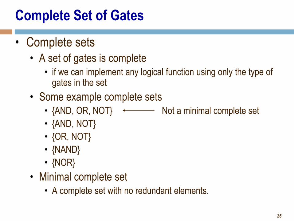
Complete Set of Gates
• Complete sets • A set of gates is complete
• if we can implement any logical function using only the type of gates in the set
• Some example complete sets • {AND, OR, NOT} Not a minimal complete set
• {AND, NOT}
• {OR, NOT}
• {NAND}
• {NOR}
• Minimal complete set • A complete set with no redundant elements.
26
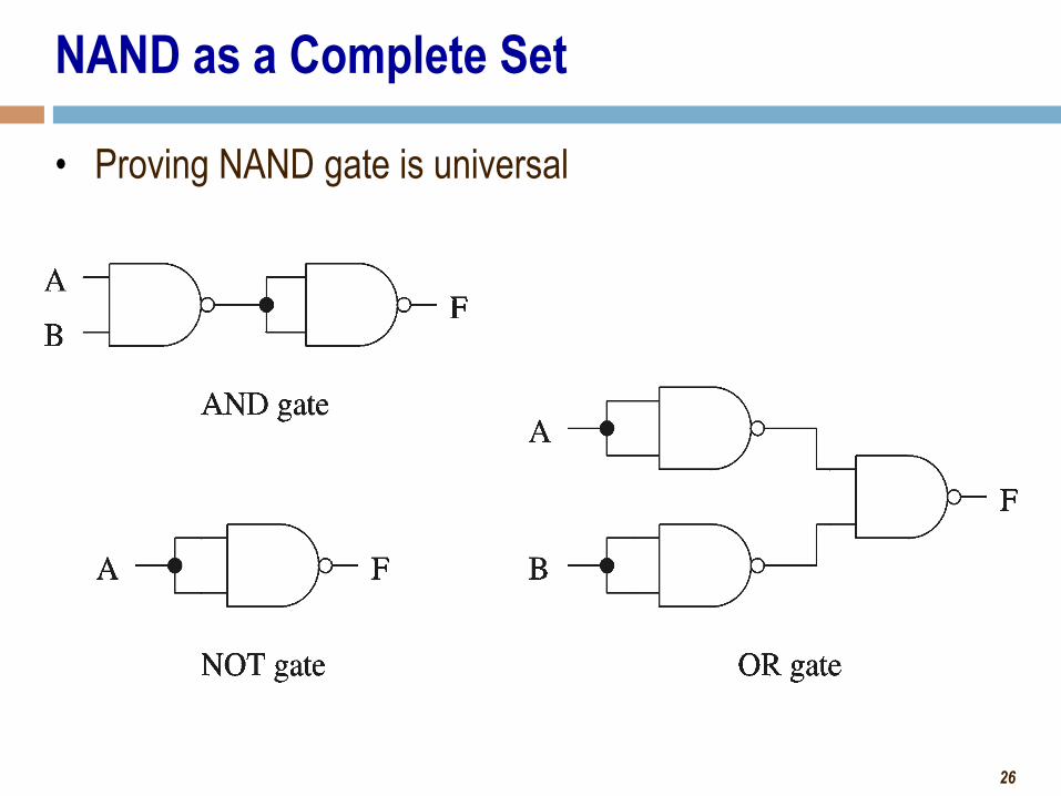
NAND as a Complete Set
• Proving NAND gate is universal
27
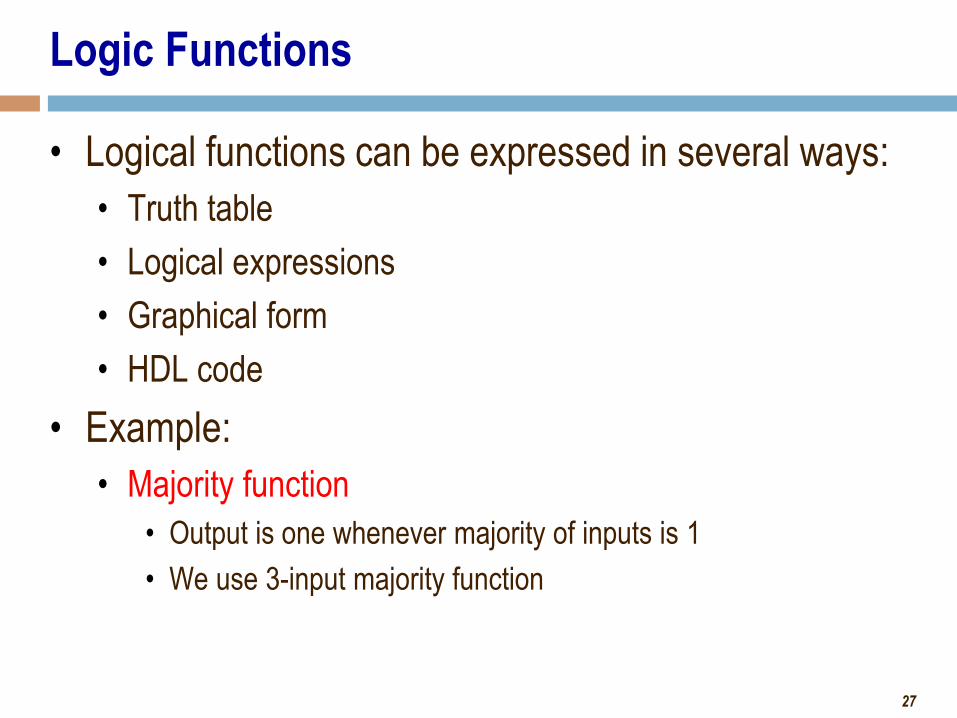
Logic Functions
• Logical functions can be expressed in several ways:
• Truth table
• Logical expressions
• Graphical form
• HDL code
• Example:
• Majority function
• Output is one whenever majority of inputs is 1
• We use 3-input majority function

28
Logic Functions (cont’d)
Truth table A B C F
0 0 0 0
0 0 1 0
0 1 0 0
0 1 1 1
1 0 0 0
1 0 1 1
1 1 0 1
1 1 1 1
Logical expression form
F = A B + B C + A C
Graphical schematic form
29
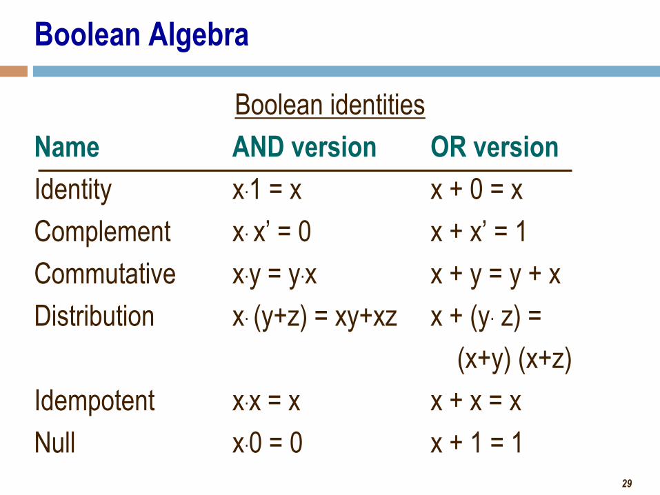
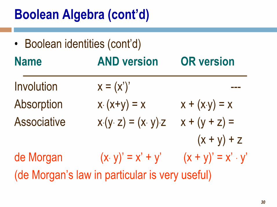
Boolean Algebra
Boolean identities
Name AND version OR version
Identity x.1 = x x + 0 = x
Complement x. x’ = 0 x + x’ = 1
Commutative x.y = y.x x + y = y + x
Distribution x. (y+z) = xy+xz x + (y. z) =
(x+y) (x+z)
Idempotent x.x = x x + x = x
Null x.0 = 0 x + 1 = 1
30
Boolean Algebra (cont’d)
• Boolean identities (cont’d)
Name AND version OR version
Involution x = (x’)’ ---
Absorption x. (x+y) = x x + (x.y) = x
Associative x.(y. z) = (x. y).z x + (y + z) =
(x + y) + z
de Morgan (x. y)’ = x’ + y’ (x + y)’ = x’ . y’
(de Morgan’s law in particular is very useful)
31
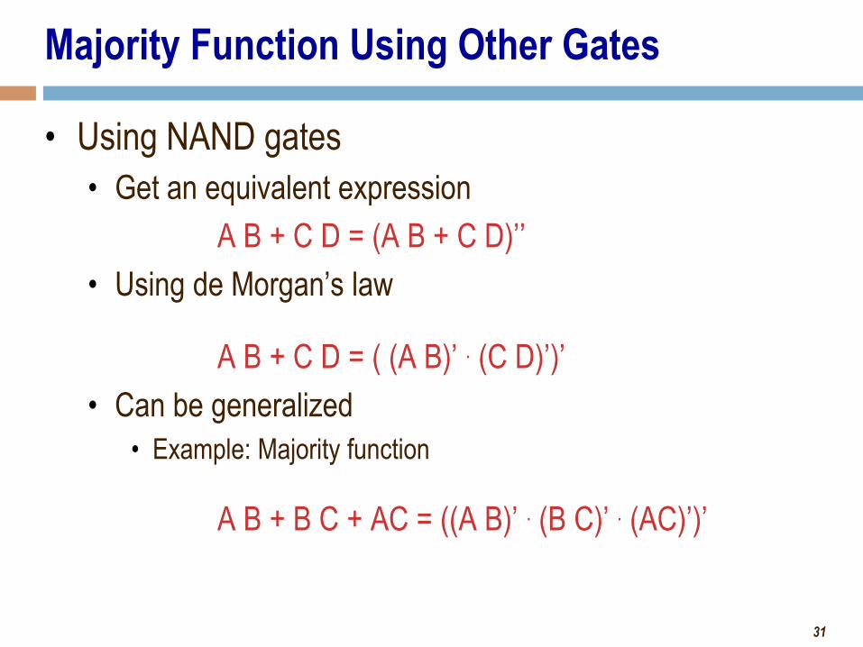
Majority Function Using Other Gates
• Using NAND gates
• Get an equivalent expression
A B + C D = (A B + C D)’’
• Using de Morgan’s law
A B + C D = ( (A B)’ . (C D)’)’
• Can be generalized
• Example: Majority function
A B + B C + AC = ((A B)’ . (B C)’ . (AC)’)’
32
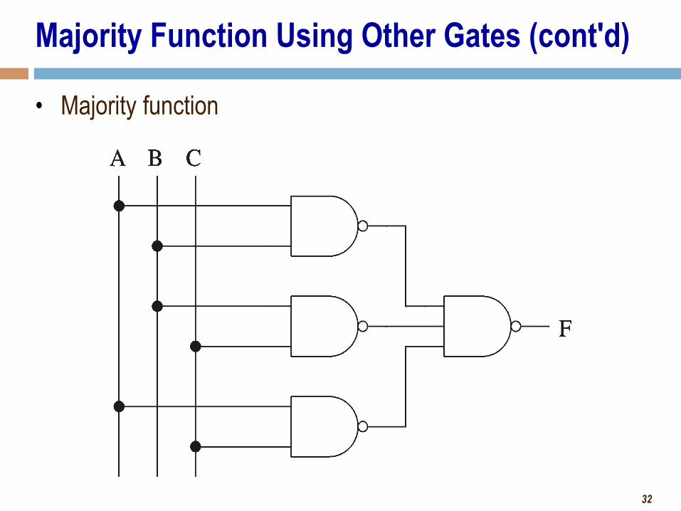
Majority Function Using Other Gates (cont'd)
• Majority function
33
Combinational Logic Building Blocks
34
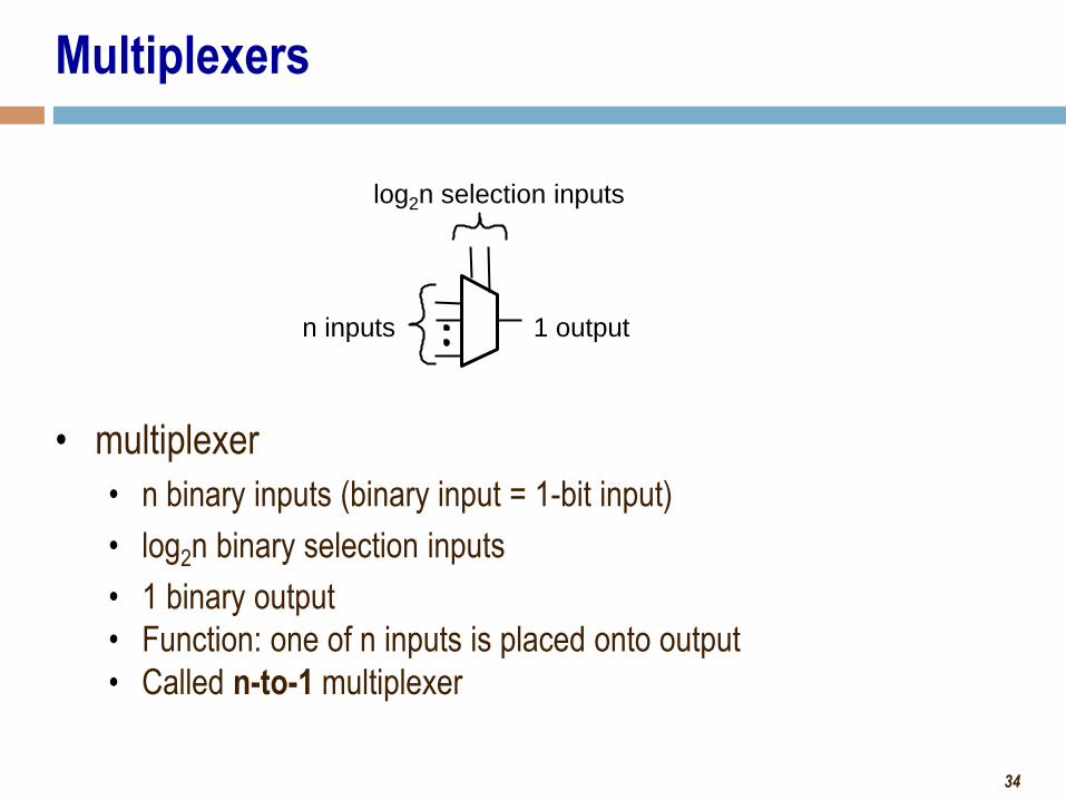
Multiplexers
• multiplexer
• n binary inputs (binary input = 1-bit input)
• log2n binary selection inputs
• 1 binary output
• Function: one of n inputs is placed onto output
• Called n-to-1 multiplexer
n inputs 1 output
log2n selection inputs
35
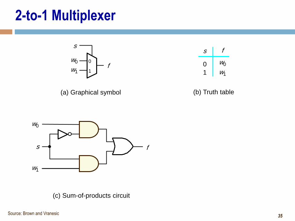
2-to-1 Multiplexer
(a) Graphical symbol
f
s
w 0
w 1
0
1
(b) Truth table
0
1
f
f s
w 0
w 1
(c) Sum-of-products circuit
s
w 0
w 1
Source: Brown and Vranesic
36
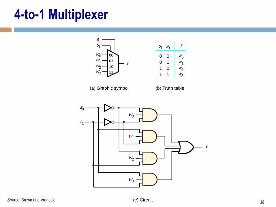
4-to-1 Multiplexer
f
s 1
w 0 w 1
00
01
(b) Truth table
w 0
w 1
s 0
w 2 w 3
10
11
0
0
1
1
1
0
1
f s 1
0
s 0
w 2
w 3
f
(c) Circuit
s 1
w 0
w 1
s 0
w 2
w 3
(a) Graphic symbol
Source: Brown and Vranesic
37
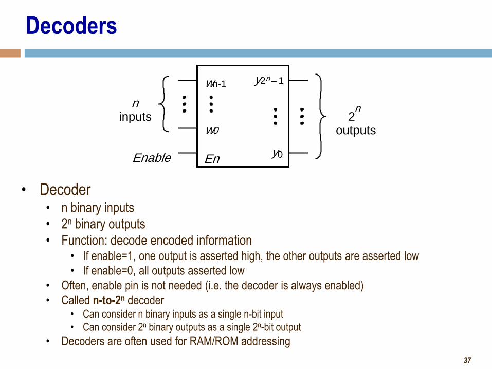
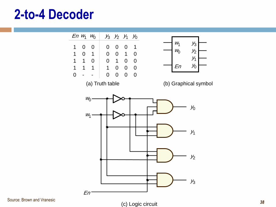
Decoders
• Decoder • n binary inputs
• 2n binary outputs
• Function: decode encoded information • If enable=1, one output is asserted high, the other outputs are asserted low
• If enable=0, all outputs asserted low
• Often, enable pin is not needed (i.e. the decoder is always enabled)
• Called n-to-2n decoder • Can consider n binary inputs as a single n-bit input
• Can consider 2n binary outputs as a single 2n-bit output
• Decoders are often used for RAM/ROM addressing
n-1
w 0
n inputs
En Enable
2 n
outputs
y 0
w y 2 n 1 –
38
2-to-4 Decoder
0
0
1
1
1
0
1
y 3 w 1
0
w 0
(c) Logic circuit
w 1
w 0
- -
1
1
0
1
1
En
0
0
1
0
0
y 2
0
1
0
0
0
y 1
1
0
0
0
0
y 0
0
0
0
1
0
y 0
y 1
y 2
y 3
En
w 1
En
y 3
w 0 y 2
y 1
y 0
(a) Truth table (b) Graphical symbol
Source: Brown and Vranesic
39
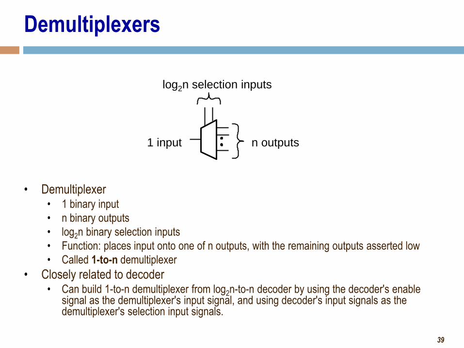
Demultiplexers
• Demultiplexer • 1 binary input
• n binary outputs
• log2n binary selection inputs
• Function: places input onto one of n outputs, with the remaining outputs asserted low
• Called 1-to-n demultiplexer
• Closely related to decoder • Can build 1-to-n demultiplexer from log2n-to-n decoder by using the decoder's enable
signal as the demultiplexer's input signal, and using decoder's input signals as the demultiplexer's selection input signals.
n outputs 1 input
log2n selection inputs
40
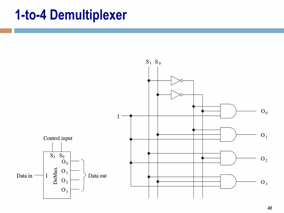
1-to-4 Demultiplexer
41
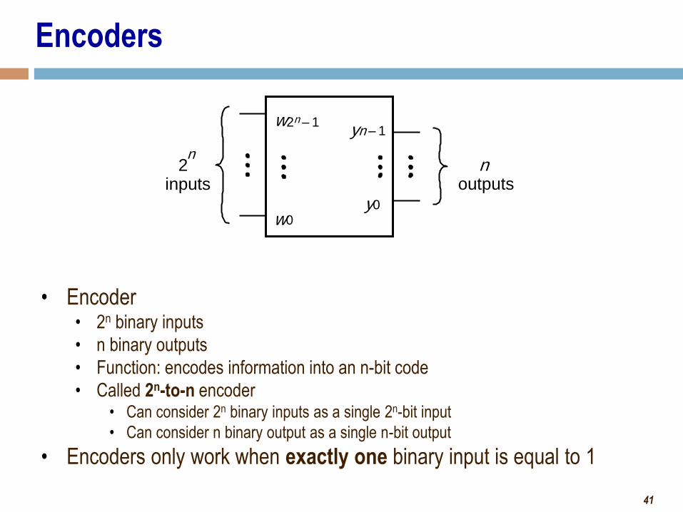
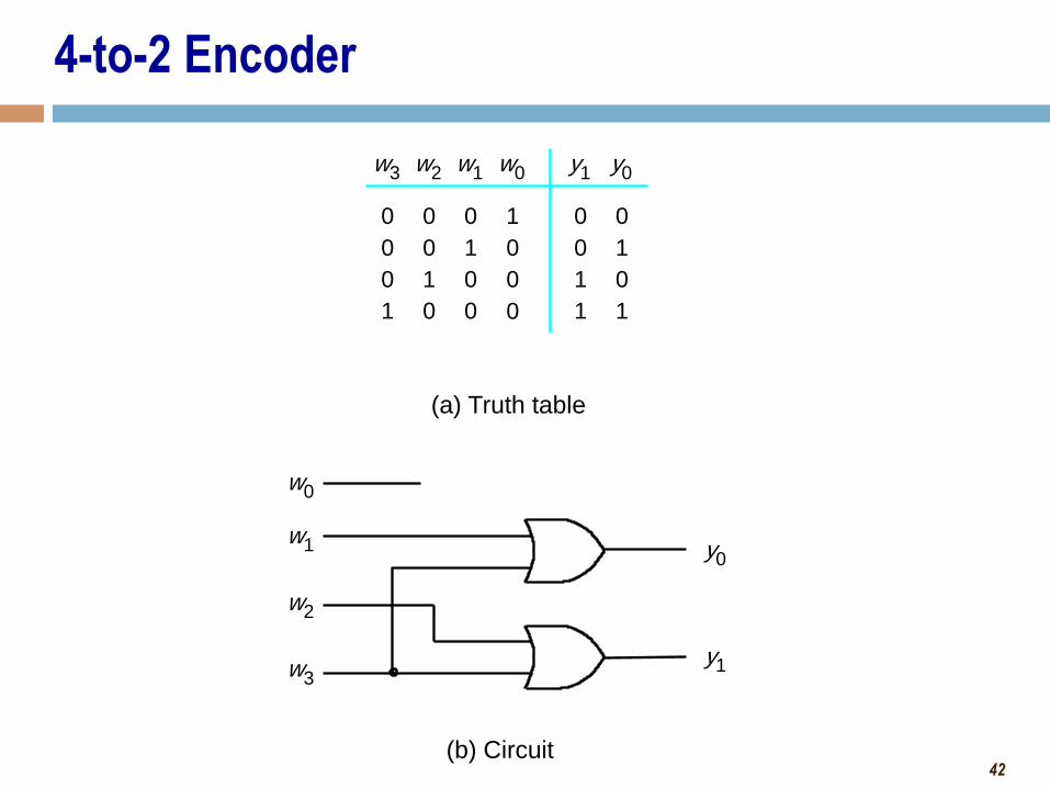
Encoders
2 n
inputs
w 0 y 0
y n 1 –
n outputs
• Encoder • 2n binary inputs
• n binary outputs
• Function: encodes information into an n-bit code
• Called 2n-to-n encoder • Can consider 2n binary inputs as a single 2n-bit input
• Can consider n binary output as a single n-bit output
• Encoders only work when exactly one binary input is equal to 1
w 2 n 1 –
42
4-to-2 Encoder
0
0
1
1
1
0
1
w 3 y 1
0
y 0
(b) Circuit
w 1
w 0
0
0
1
0
w 2
0
1
0
0
w 1
1
0
0
0
w 0
0
0
0
1
y 0
w 2
w 3 y 1
(a) Truth table

43
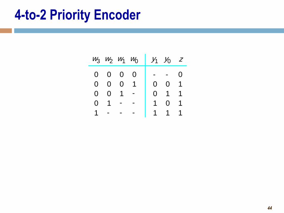
Priority Encoders
2 n
inputs
w 0
w 2 n 1 –
y 0
y n 1 –
n outputs
• Priority Encoder • 2n binary inputs
• n binary outputs
• 1 binary "valid" output
• Function: encodes information into an n-bit code based on priority of inputs
• Called 2n-to-n priority encoder
• Priority encoder allows for multiple inputs to have a value of '1', as it encodes the input with the highest priority (MSB = highest priority, LSB = lowest priority)
• "valid" output indicates when priority encoder output is valid
• Priority encoder is more common than an encoder
z "valid" output
44
4-to-2 Priority Encoder
-
0
0
1
0
1
0
w 0 y 1
-
y 0
1 1
0
1
1
1
1
z
1
-
-
0
-
w 1
0
1
-
0
-
w 2
0
0
1
0
-
w 3
0
0
0
0
1
45
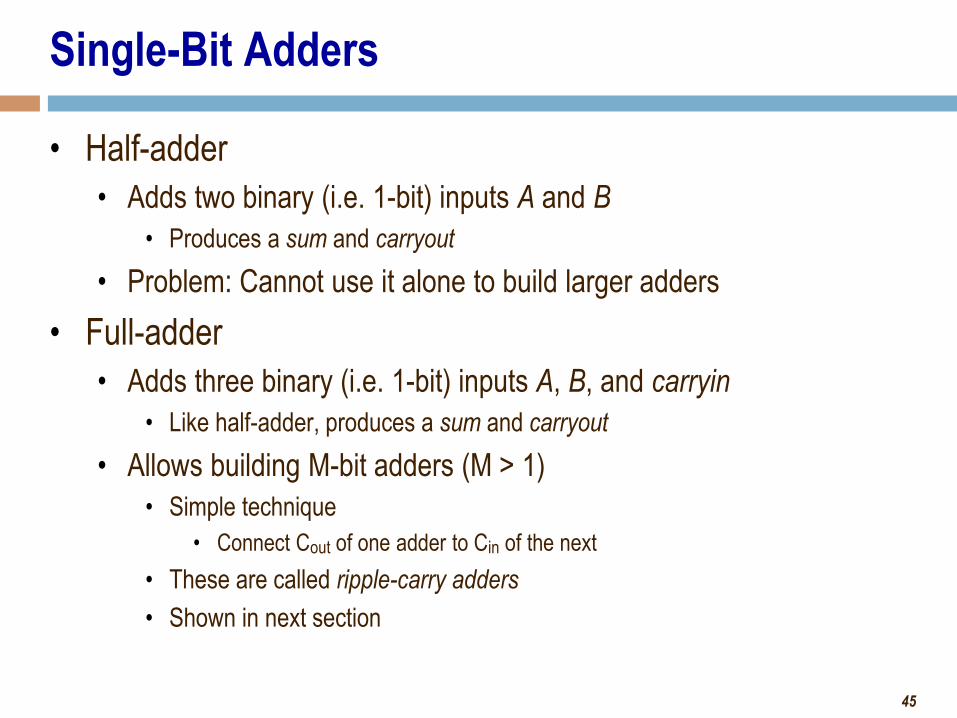
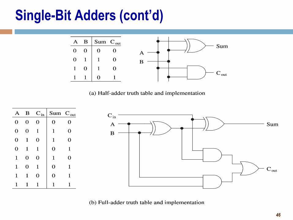
Single-Bit Adders
• Half-adder
• Adds two binary (i.e. 1-bit) inputs A and B
• Produces a sum and carryout
• Problem: Cannot use it alone to build larger adders
• Full-adder
• Adds three binary (i.e. 1-bit) inputs A, B, and carryin
• Like half-adder, produces a sum and carryout
• Allows building M-bit adders (M > 1)
• Simple technique
• Connect Cout of one adder to Cin of the next
• These are called ripple-carry adders
• Shown in next section
46
Single-Bit Adders (cont’d)
47
Multi-Bit Combinational Logic Building
Blocks
48
Multi-bit 4-to-1 Multiplexer
• When drawing schematics, can draw multi-bit multiplexers
• Example: 4-to-1 (8 bit) multiplexer
• 4 inputs (each 8 bits)
• 1 output (8 bits)
• 2 selection bits
• Can also have multi-bit 2-to-1 muxes, 16-to-1 muxes, etc.
f
s 1
w 0 w 1
00
01
(b) Truth table
w 0
w 1
s 0
w 2 w 3
10
11
0
0
1
1
1
0
1
f s 1
0
s 0
w 2
w 3
(a) Graphic symbol
8
8

49
4-to-1 (8-bit) Multiplexer
f(7)
s 1
00
01
s 0
10
11
f(6)
s 1
00
01
s 0
10
11
f(0)
s 1
00
01
s 0
10
11
w0(7)
w1(7)
w2(7)
w3(7)
w0(6)
w1(6)
w2(6)
w3(6)
w0(0)
w1(0)
w2(0)
w3(0)
A 4-to-1 (8-bit) multiplexer is composed
of eight 4-to-1 (1-bit) multiplexers
f
s 1
w 0 w 1
00
01
s 0
w 2 w 3
10
11
8
8
=
50
16-bit Unsigned Adder
16 16
X Y
16
Cin Cout
S
51
Multi-Bit Ripple-Carry Adder
A 16-bit ripple-carry adder is composed of 16 (1-bit) full adders
Inputs: 16-bit A, 16-bit B, 1-bit carryin (set to zero in the figure below)
Outputs: 16-bit sum R, 1-bit overflow
Other multi-bit adder structures can be studied in ECE 645—Computer Arithmetic
Called a ripple-carry adder because carry ripples from one full-adder to the next.
Critical path is 16 full-adders.
52
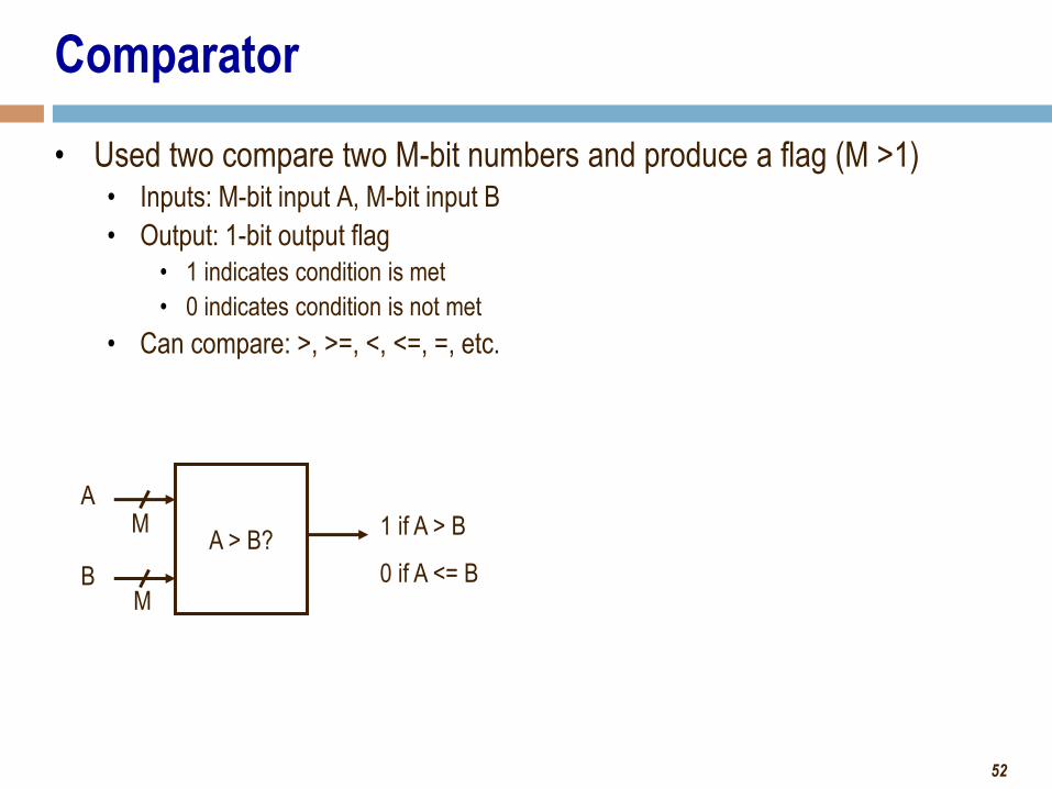
Comparator
• Used two compare two M-bit numbers and produce a flag (M >1) • Inputs: M-bit input A, M-bit input B
• Output: 1-bit output flag
• 1 indicates condition is met
• 0 indicates condition is not met
• Can compare: >, >=, <, <=, =, etc.
A > B?
A
B
1 if A > B
0 if A <= B
M
M
53
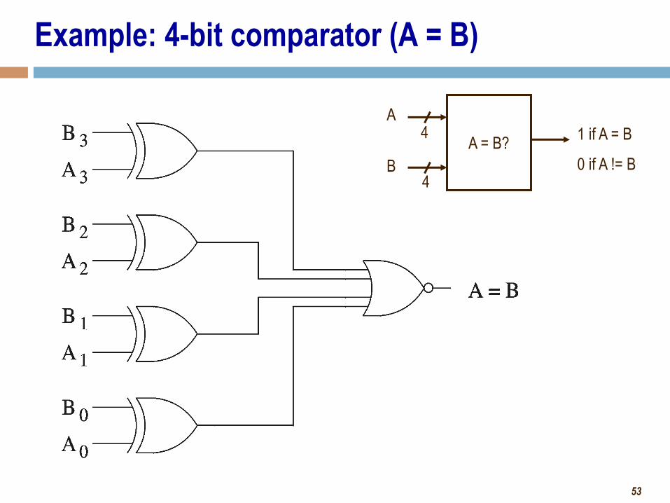
Example: 4-bit comparator (A = B)
A = B?
A
B
1 if A = B
0 if A != B
4
4
54
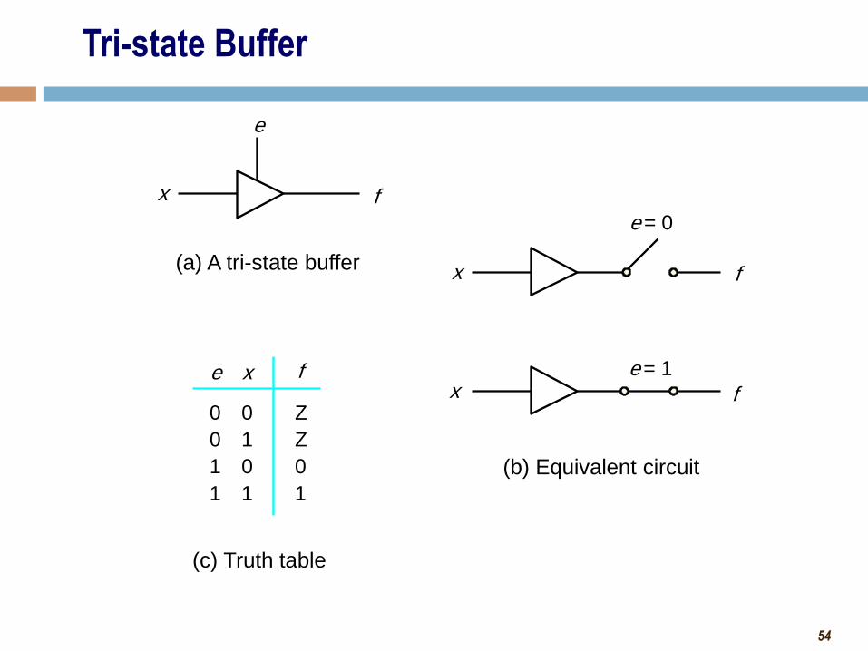
(b) Equivalent circuit
(c) Truth table
x f
e
(a) A tri-state buffer
0
0
1
1
0
1
0
1
Z
Z
0
1
f e x
x f
e = 0
e = 1 x f
Tri-state Buffer
55
x f
e
(b)
x f
e
(a)
x f
e
(c)
x f
e
(d)
Four types of Tri-state Buffers
56
Sequential Logic Building Blocks
some slides modified from:
Brown and Vranesic, ―Fundamentals of Digital Logic with VHDL Design, 2nd Edition‖
S. Dandamudi, ―Fundamentals of Computer Organization and Design‖
57
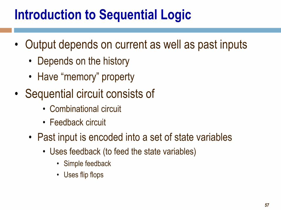
Introduction to Sequential Logic
• Output depends on current as well as past inputs
• Depends on the history
• Have “memory” property
• Sequential circuit consists of • Combinational circuit
• Feedback circuit
• Past input is encoded into a set of state variables
• Uses feedback (to feed the state variables)
• Simple feedback
• Uses flip flops
58
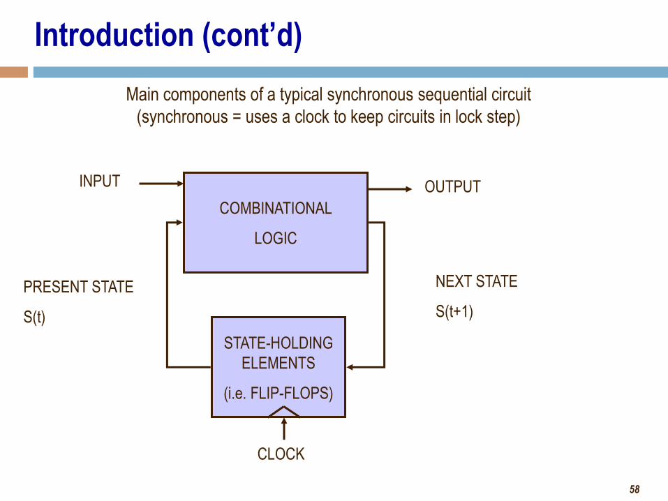
Introduction (cont’d)
Main components of a typical synchronous sequential circuit
(synchronous = uses a clock to keep circuits in lock step)
COMBINATIONAL
LOGIC
STATE-HOLDING
ELEMENTS
(i.e. FLIP-FLOPS)
CLOCK
INPUT OUTPUT
NEXT STATE
S(t+1)
PRESENT STATE
S(t)
59
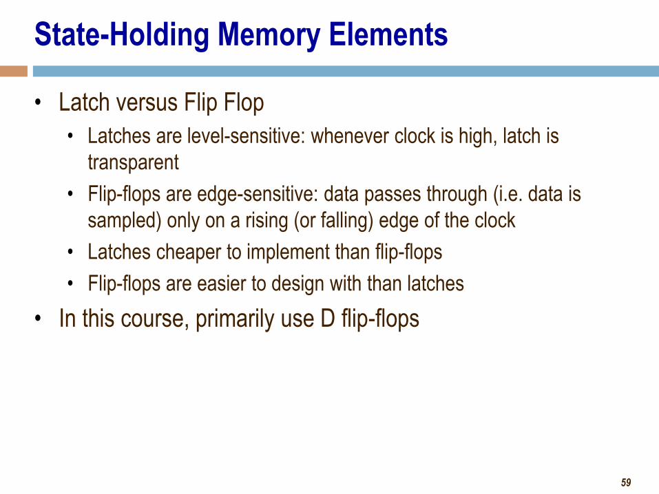
State-Holding Memory Elements
• Latch versus Flip Flop
• Latches are level-sensitive: whenever clock is high, latch is
transparent
• Flip-flops are edge-sensitive: data passes through (i.e. data is
sampled) only on a rising (or falling) edge of the clock
• Latches cheaper to implement than flip-flops
• Flip-flops are easier to design with than latches
• In this course, primarily use D flip-flops

60
D Latch vs. D Flip-Flop
Latch transparent when clock is high
“Samples” D on rising edge of clock
D Q
CLK
D Q
CLK
D
CLK
Q
D
CLK
Q
61
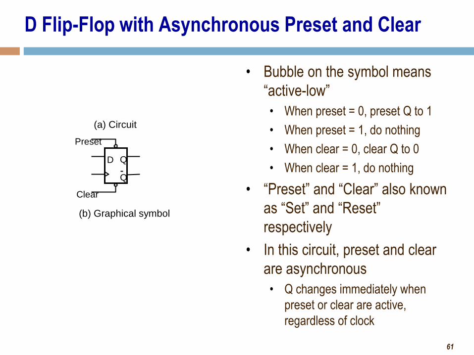
D Flip-Flop with Asynchronous Preset and Clear
• Bubble on the symbol means
“active-low”
• When preset = 0, preset Q to 1
• When preset = 1, do nothing
• When clear = 0, clear Q to 0
• When clear = 1, do nothing
• “Preset” and “Clear” also known
as “Set” and “Reset”
respectively
• In this circuit, preset and clear
are asynchronous
• Q changes immediately when
preset or clear are active,
regardless of clock
Preset
Clear
(a) Circuit
(b) Graphical symbol
D Q
Q
62
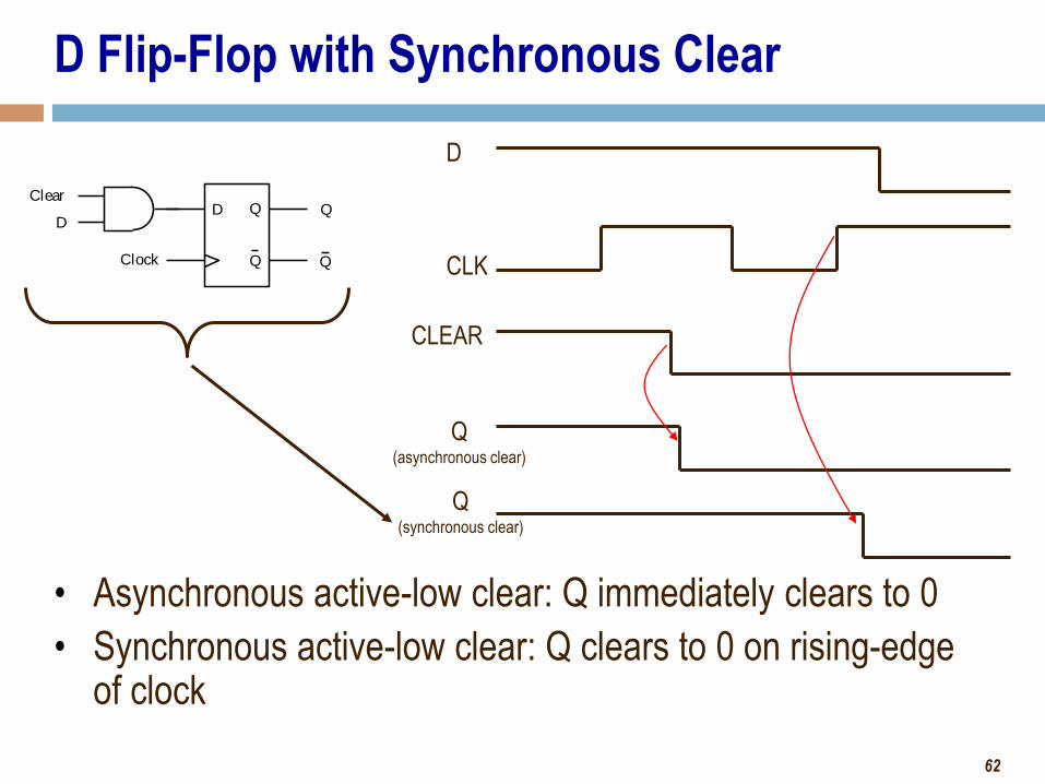
D Flip-Flop with Synchronous Clear
• Asynchronous active-low clear: Q immediately clears to 0
• Synchronous active-low clear: Q clears to 0 on rising-edge of clock
D
Clock Q
QClear
D Q
Q
D
CLK
CLEAR
Q (asynchronous clear)
Q (synchronous clear)
63
Sequential Logic Circuits
some slides modified from:
Brown and Vranesic, ―Fundamentals of Digital Logic with VHDL Design, 2nd Edition‖
S. Dandamudi, ―Fundamentals of Computer Organization and Design‖
64
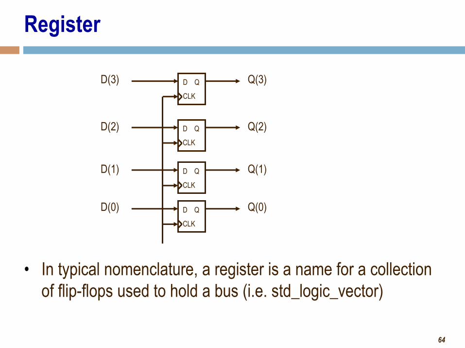
Register
• In typical nomenclature, a register is a name for a collection
of flip-flops used to hold a bus (i.e. std_logic_vector)
D Q
CLK
D Q
CLK
D Q
CLK
D Q
CLK
D(3)
D(2)
D(1)
D(0)
Q(3)
Q(2)
Q(1)
Q(0)

65
Shift Register
D Q
Q Clk
D Q
Q
D Q
Q
D Q
Q
Sin Q
t 0
t 1
t 2
t 3
t 4
t 5
t 6
t 7
1
0
1
1
1
0
0
0
0
1
0
1
1
1
0
0
0
0
1
0
1
1
1
0
0
0
0
1
0
1
1
1
0
0
0
0
1
0
1
1
Q 1 Q 2 Q 3 Q 4 Q = Sin
(b) A sample sequence
(a) Circuit
Q 1 Q 2 Q 3 Q 4
SHIFT
REGISTER Sin
Clk
Q
66
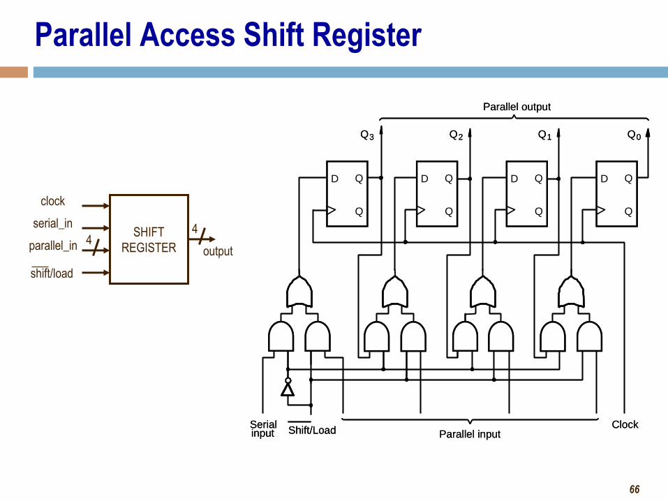
Parallel Access Shift Register
Q3 Q2 Q1 Q0
ClockParallel input
Parallel output
Shift/LoadSerialinput
D Q
Q
D Q
Q
D Q
Q
D Q
Q
Q3 Q2 Q1 Q0
ClockParallel input
Parallel output
Shift/LoadSerialinput
D Q
Q
D Q
Q
D Q
Q
D Q
Q
SHIFT
REGISTER
serial_in
clock
parallel_in 4
shift/load
output
4
67
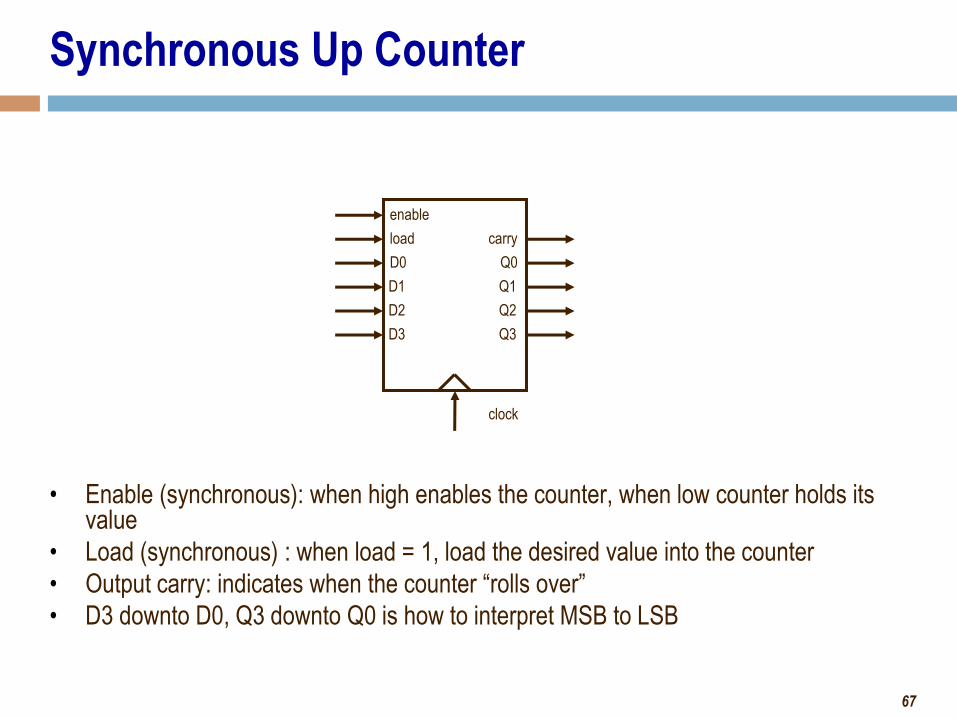
Synchronous Up Counter
• Enable (synchronous): when high enables the counter, when low counter holds its value
• Load (synchronous) : when load = 1, load the desired value into the counter
• Output carry: indicates when the counter “rolls over”
• D3 downto D0, Q3 downto Q0 is how to interpret MSB to LSB
enable
load
D0
D1
D2
D3
Q0
Q1
Q2
Q3
clock
carry
68
Memories
some slides modified from:
Brown and Vranesic, ―Fundamentals of Digital Logic with VHDL Design, 2nd Edition‖
S. Dandamudi, ―Fundamentals of Computer Organization and Design‖
69
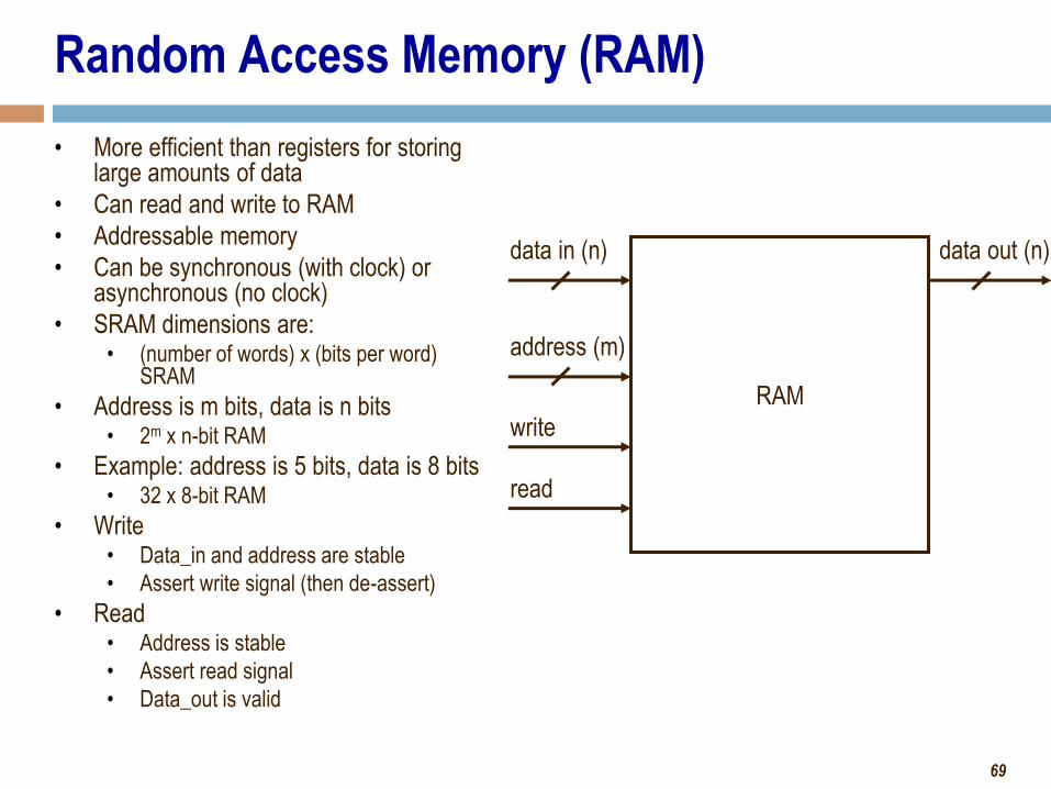
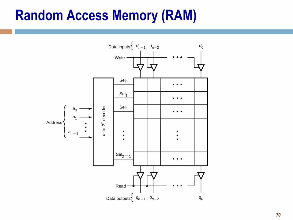
Random Access Memory (RAM)
• More efficient than registers for storing large amounts of data
• Can read and write to RAM
• Addressable memory
• Can be synchronous (with clock) or asynchronous (no clock)
• SRAM dimensions are: • (number of words) x (bits per word)
SRAM
• Address is m bits, data is n bits • 2m x n-bit RAM
• Example: address is 5 bits, data is 8 bits • 32 x 8-bit RAM
• Write • Data_in and address are stable
• Assert write signal (then de-assert)
• Read • Address is stable
• Assert read signal
• Data_out is valid
RAM
data in (n)
address (m)
data out (n)
write
read
70
Random Access Memory (RAM)
Sel 2
Sel 1
Sel 0
Sel 2 m 1 ”
Read
Write
d 0 d n 1 – d n 2 –
q 0 q n 1 – q n 2 –
m -to
-2 m
de
code
r
Address
a 0
a 1
a m 1 –
Data outputs
Data inputs

71
Read Only Memory (ROM)
• Similar to RAM except
read only
• Addressable memory
• Can be synchronous
(with clock) or
asynchronous (no
clock)
ROM
address (m) data out (n)
read
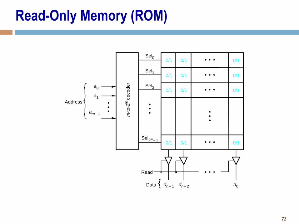
72
Read-Only Memory (ROM)
Sel 2
Sel 1
Sel 0
Sel 2 m 1 –
Address
Read
d 0 d n 1 – d n 2 –
m -to-2
m d
eco
der
0/1 0/1 0/1
0/1 0/1 0/1
0/1 0/1 0/1
0/1 0/1 0/1
Data
a 0
a 1
a m 1 –