Embed Size (px)
Citation preview
Wafer-Edge Challenges
SEMI STEP Wafer Edge Profile
SEMICON/West 2006
Tetsuo Fukuda SEMI Japan (Fujitsu)
Japan Advanced Wafer Geometry Task Force
SEMI Japan
Abstract Issues on edge profile are discussed and the standardization is strongly emphasized from the
point of requirements in wafer production and device fabrication process. Since the current SEMI M1 standard specifies a very broad range of edge profiles, many
types have been allowed to be used in the market. In device fabrication process, the most serious issue related to wafer edge is particle generation, which results from residual film coming off at the edge. To remove remaining film, edge polishing and/or edge etching have been effectively employed.
In the next generation (45nm), edge polishing will be more essential than before because a new material, hafnium oxide (HfO), will be applied as a gate dielectric film, replaced with silicon dioxide (SiO2) film. It is quite difficult to remove HfO film completely by etching technique on the wafer surface except transistor gate electrodes. This severely requires edge polishing rather than etching technique in removing residual HfO film at wafer edge.
However, a suitable condition of edge polishing depends on edge profile. The polishing condition oriented to round edge does not bring high performance for blunt edge.
First, this requires the unification of edge profile at least in one fabrication line of the next generation. Second, suitable metric should be standardized for the edge profile. Single, two, or at most three types of edge profile is to be discussed for standardization.
Biography Tetsuo Fukuda Manager of Electronic Devices Group FUJITSU Akiruno Technology Center
Tetsuo Fukuda was born in Japan in 1955. He received his M. S. degree from Keio University in Tokyo. He joined FUJITSU Ltd. in 1981 and has engaged in the R & D of wafer process technologies. He earned his Ph. D. in Applied Physics from Keio University in 1997.
He was awarded the International Collaboration Award from SEMI in 2001. He has been a chairman of the Next Generation Wafer Technologies Subcommittee in Japan Electronics and Information Technology Industries Association (JEITA), and also a co-chair of Japan Advanced Wafer Geometry Task Force in SEMI. Contact information Tetsuo Fukuda Manager of Electronic Devices Group FUJITSU Akiruno Techonology Center 50 Fuchigami, Akiruno, Tokyo 197-0833, Japan Email: [email protected]

Notes
__________________________________________________________________
__________________________________________________________________
__________________________________________________________________
__________________________________________________________________
__________________________________________________________________
__________________________________________________________________
__________________________________________________________________
__________________________________________________________________
__________________________________________________________________
__________________________________________________________________
__________________________________________________________________
__________________________________________________________________
__________________________________________________________________
__________________________________________________________________
__________________________________________________________________
__________________________________________________________________
__________________________________________________________________
__________________________________________________________________
The Wafer Edge:New Challenges
Andre AndrukhivAndre AndrukhivKomatsu Silicon AmericaKomatsu Silicon America
SEMI STEP Wafer Edge Profile MeetingSEMI STEP Wafer Edge Profile Meeting
SEMICON WEST 2006SEMICON WEST 2006
July 12, 2006July 12, 2006
Abstract ITRS continues relentless pursuit of perfection in wafer geometry driven by lithograhy requirements. Roadmap is also squeezing more usable area from the wafer. Edge exclusion is going from 2mm to 1.5mm in 2007. To produce wafers for the next technology generations, metrology must be capable. Modern optical metrology is fundamentally up to the challenge. Short overview of edge related issues: Edge Roll Off, Edge Profile, edge defects. Are new metrics needed for the edge? Traditional metrics work well in central region of wafer but not designed for edge. New edge metrics proposed - need to be qualified. Many choices - need simplicity and clarity. With new lithography, new metrics are needed? Edge specific CMP metric - curvature. Challenges for wafer manufactures—“universal” wafer edge that works for all customers.
Biography Andre Andrukhiv, Ph. D. Komatsu Silicon America
Andre Andrukhiv is a Senior Applications Engineer at Komatsu Silicon America (KSA) since 1999, responsible for technical support of major US customers. In this role, he also managed and coordinated numerous projects resulted in development advanced metrology for Silicon wafers manufacturing. Prior to that worked as Senior Process Engineer in crystal growth operation during KSA’s wafer fab start-up in Hillsboro, OR. As one of the company’s liaisons to the semiconductor industry he has been participated in various technical organizations including SEMI, ASTM, SiWEDS (currently co-chairman of IAB-Industrial Advisory Board). Before joining KSA, Andrukhiv worked as assistant professor of physics and electronics, and principal researcher in Drohobych State University (Ukraine). Conducted research projects on electronic structure and photoelectric properties of narrow-gap semiconductors authored various scientific publications in international refereed journals and conferences. He earned his MS in Physics and Semiconductor Electronics from the Lviv State University, Ukraine, and Ph.D. in Physics of Semiconductors from the Ioffe Institute, Russian Academy of Sciences. Andrukhiv is a member of the American Physical Society, IEEE, and The Electrochemical Society

Notes
__________________________________________________________________
__________________________________________________________________
__________________________________________________________________
__________________________________________________________________
__________________________________________________________________
__________________________________________________________________
__________________________________________________________________
__________________________________________________________________
__________________________________________________________________
__________________________________________________________________
__________________________________________________________________
__________________________________________________________________
__________________________________________________________________
__________________________________________________________________
__________________________________________________________________
__________________________________________________________________
__________________________________________________________________
__________________________________________________________________
Edge Profile CreationSubsurface Damage Issues
SEMI STEP Wafer Edge Profile
SEMICON/West 2006
Vladimir RivaAccretech USA
July 12, 2006
Abstract
Accretech continues research and development in a critical aspect of maintaining the edge profile geometry and sub-surface damage minimization.
This paper will present the following aspects:
- sub-surface damage creation and removal during wafer fabrication;
- correlation between sub-surface damage and surface roughness;
- method of maintaining the edge profile geometry during sub-surface damage removal.

Biography Vladimir Riva, Engineering Manager, WMS Accretech USA
Vladimir Riva is currently an engineering manager of a Wafer Mfg. Systems division of Accretech USA in Lincoln Park, NJ. He has been in machinery design engineering for over 25-years. He develops wafer edge profiling systems for semiconductor industry for over 10 years. He is a member of SEMI Edge Profile Working Group.

Notes
__________________________________________________________________
__________________________________________________________________
__________________________________________________________________
__________________________________________________________________
__________________________________________________________________
__________________________________________________________________
__________________________________________________________________
__________________________________________________________________
__________________________________________________________________
__________________________________________________________________
__________________________________________________________________
__________________________________________________________________
__________________________________________________________________
__________________________________________________________________
__________________________________________________________________
__________________________________________________________________
__________________________________________________________________
__________________________________________________________________
Edge Profile Parametersof Silicon Wafers
Thomas Becker
KoCoS Optical Measurement GmbH
Germany
www.kocos-optics.com
Abstract Rounding the edges of silicon wafers serves primarily to reduce their susceptibility to chipping during subsequent processing. It also helps to keep epitaxial edge crown and photoresist edge bead to a minimum. It is important that edge profiles are as homogenous as possible both on the circumference of the wafer and in the notch area. The geometrical characterisation of edge profiles requires high-precision measuring equipment using various different measurement methods, including techniques based on profile projection and light-sectioning technology. While both measurement methods are non-destructive, they each feature different advantages and disadvantages. The combination of both methods allows an optimum characterisation of wafer edge geometry. This presentation gives an introduction to characteristic edge geometry parameters and an overview of the principles and capabilities of the two methods mentioned above.
Biography Thomas Becker KoCoS Optical Measurement GmbH, Germany While studying electrical engineering, Thomas Becker’s main interest lay in the area of measuring and testing. A wealth of excellent ideas and the ability to develop ideal solutions for their technical implementation led him to found KoCoS Messtechnik AG in 1988. The company quickly gained a foothold in the market with the high quality of its measurement and test technology for the power engineering sector. Today the company is a leader in its field. Thomas Becker’s focus always lies on what is technically possible and his approach to complex physical problems is to view them as a challenge. KoCoS Optical Measurement GmbH, founded by Thomas Becker in 2000, provides advanced technology for the precise determination of geometrical quantities in the industrial manufacturing sector. Thomas Becker is in charge of all new product development projects, including systems specializing in the measurement of wafer edge profiles.

Notes
__________________________________________________________________
__________________________________________________________________
__________________________________________________________________
__________________________________________________________________
__________________________________________________________________
__________________________________________________________________
__________________________________________________________________
__________________________________________________________________
__________________________________________________________________
__________________________________________________________________
__________________________________________________________________
__________________________________________________________________
__________________________________________________________________
__________________________________________________________________
__________________________________________________________________
__________________________________________________________________
__________________________________________________________________
__________________________________________________________________
Wafer-Edge Descriptions in Defect Detection
Milton GodwinInternational SEMATECH Manufacturing Initiative
(ISMI)
Abstract ISMI Defect Metrology has sponsored a working group for vendors of wafer-edge defect detection tools. In seeking common nomenclature and data formats within the defect detection community, terms for edge and bevel regions have been generated which may not correspond to SEMI's Edge Profile Standards initiative. This paper will present the terminology of edge regions currently employed by the defect detection community and compare them to the SEMI initiative in the hopes to achieve consensus and a common naming system.
Biography Milton Godwin, Consulting Engineer SEMATECH
Milton Godwin is currently a consulting engineer for the International SEMATECH Manufacturing Initiative (ISMI) in Austin, Texas. He has been in yield engineering and yield management throughout his 28-year career in the semiconductor industry. He has been Yield Manager for Fairchild Center, National Semiconductor and managed SEMATECH sponsorship and testing in the development of the KLA-Tencor AIT. He led applications introduction of the AMAT PDC defect detection/review tool set. He is currently supervising the construction of intentional defect standards for ISMI.

Notes
__________________________________________________________________
__________________________________________________________________
__________________________________________________________________
__________________________________________________________________
__________________________________________________________________
__________________________________________________________________
__________________________________________________________________
__________________________________________________________________
__________________________________________________________________
__________________________________________________________________
__________________________________________________________________
__________________________________________________________________
__________________________________________________________________
__________________________________________________________________
__________________________________________________________________
__________________________________________________________________
__________________________________________________________________
__________________________________________________________________
SEMI Wafer Edge Profile SurveySEMI Wafer Edge Profile Survey
Dr. Paul H. LangerDr. Paul H. LangerKomatsuKomatsu Silicon AmericaSilicon America
andandMasanori YoshiseMasanori Yoshise
ADEADE--JapanJapan
SEMI InternationalSEMI InternationalAdvanced Wafer Geometry TFAdvanced Wafer Geometry TF
SEMI Edge Profile WGSEMI Edge Profile WG
Abstract A survey was designed and distributed to device manufacturers in Japan and the US in order to solicit their views on the need for a more precise characterization of the silicon wafer edge profile. It is believed that the current edge profile template described in SEMI M1 is inadequate to fully describe the edge region of the wafer so that many different edge profiles pass the SEMI template test leading to a variety of process issues related this variety of different edge shapes. SEMI formed the Edge Profile Working Group in order to investigate if a better and more precise definition of the wafer edge was now required as the edge exclusion continues to shrink. The goal of this group was to determine whether a single edge profile would be adequate or whether the industry would be best served with an advanced “template” that would allow the production of reproducible edge profile. The 9 question survey will be discussed, and preliminary results, mainly from Japan, will be summarized. It appears from the preliminary returns that there is a significant desire to more precisely define the edge profile.
Biography Dr. Paul H. Langer Komatsu Silicon America, LLC Paul joined Komatsu Silicon America in 1995 in Applications Engineering and is currently the KSA Senior Technologist. He is responsible for technology transfer between Komatsu Electronic Metals and Komatsu Silicon America along with technical support activities for major US customers. Prior to his present position he was Director of Technology responsible for the Applications Engineering and Quality groups. Before joining Komatsu he was with AT&T Bell Laboratories for in the Silicon Research and Development group for 31 years and was responsible for Epitaxial Silicon Development and related metrologies throughout the Bell System. His standards activities started with ASTM in 1965 and he went on to chair the ASTM Committee on Electronics for 6 years and served on the ASTM Board of Directors. He has been an active member of SEMI Standards since the 1970s, and is currently the mentor to the North American Silicon Wafer Committee and chairs the Advanced Wafer Geometry and Epitaxial Silicon Wafer International Task Forces in North America.

Notes
__________________________________________________________________
__________________________________________________________________
__________________________________________________________________
__________________________________________________________________
__________________________________________________________________
__________________________________________________________________
__________________________________________________________________
__________________________________________________________________
__________________________________________________________________
__________________________________________________________________
__________________________________________________________________
__________________________________________________________________
__________________________________________________________________
__________________________________________________________________
__________________________________________________________________
__________________________________________________________________
__________________________________________________________________
__________________________________________________________________
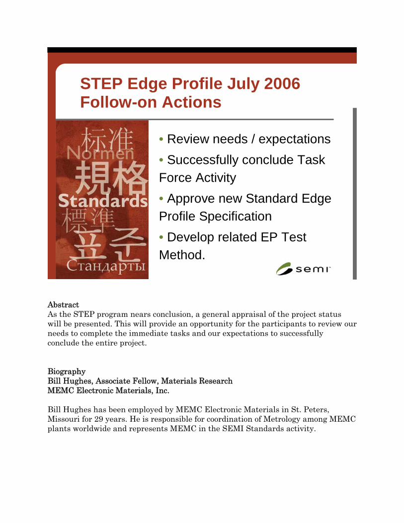
STEP Edge Profile July 2006Follow-on Actions
• Review needs / expectations• Successfully conclude Task Force Activity• Approve new Standard Edge Profile Specification• Develop related EP Test Method.
Abstract As the STEP program nears conclusion, a general appraisal of the project status will be presented. This will provide an opportunity for the participants to review our needs to complete the immediate tasks and our expectations to successfully conclude the entire project. Biography Bill Hughes, Associate Fellow, Materials Research MEMC Electronic Materials, Inc. Bill Hughes has been employed by MEMC Electronic Materials in St. Peters, Missouri for 29 years. He is responsible for coordination of Metrology among MEMC plants worldwide and represents MEMC in the SEMI Standards activity.

Notes
__________________________________________________________________
__________________________________________________________________
__________________________________________________________________
__________________________________________________________________
__________________________________________________________________
__________________________________________________________________
__________________________________________________________________
__________________________________________________________________
__________________________________________________________________
__________________________________________________________________
__________________________________________________________________
__________________________________________________________________
__________________________________________________________________
__________________________________________________________________
__________________________________________________________________
__________________________________________________________________
__________________________________________________________________
__________________________________________________________________