Embed Size (px)
Citation preview
Ruggedized Camera Encoder P14571 Hornyak, Jason, Moreno, O’Connor, StreatMay 8, 2023
CoaXPress HSMC Board Detailed Design Rev.A
Author: Lennard Streat, Computer Engineering, RIT
Multi-Disciplinary Senior Design I
RIT Ruggedized Camera Encoder (P14571)
1 | P a g e [email protected]
Ruggedized Camera Encoder P14571 Hornyak, Jason, Moreno, O’Connor, StreatMay 8, 2023
Table of Contents
1. Module 1: Custom CoaXPress HSMC Overview & Requirements Project Summary Design Overview
2. Module 2: Component Functional Descriptions Overview HSMC Interface CXP Equalizer CXP PoCXP Subsystem
3. Module 3: Specifications Maximum Ratings
4. Module 4: Application Information CXP HSMC Schematic Bill of Materials PCB Layout HSMC Pinout Test Plan
5. Module 5: Conclusion Feasibility References
2 | P a g e [email protected]

Ruggedized Camera Encoder P14571 Hornyak, Jason, Moreno, O’Connor, StreatMay 8, 2023
I. Custom CoaXPress HSMC
Overview & Requirements
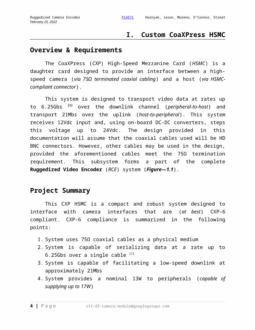
The CoaXPress (CXP) High-Speed Mezzanine Card (HSMC) is a daughter card designed to provide an interface between a high-speed camera (via 75Ω terminated coaxial cabling) and a host (via HSMC-compliant connector).
This system is designed to transport video data at rates up to 6.25Gbs [1] over the downlink channel (peripheral-to-host) and transport 21Mbs over the uplink (host-to-peripheral). This system receives 12Vdc input and, using on-board DC-DC converters, steps this voltage up to 24Vdc. The design provided in this documentation will assume that the coaxial cables used will be HD BNC connectors. However, other cables may be used in the design, provided the aforementioned cables meet the 75Ω termination requirement. This subsystem forms a part of the complete Ruggedized Video Encoder (RCE) system (Figure—1.1).
Project Summary
This CXP HSMC is a compact and robust system designed to interface with camera interfaces that are (at best) CXP-6 compliant. CXP-6 compliance is summarized in the following points:
1. System uses 75Ω coaxial cables as a physical medium2. System is capable of serializing data at a rate up to 6.25Gbs over a single cable [1]
3. System is capable of facilitating a low-speed downlink at approximately 21Mbs4. System provides a nominal 13W to peripherals (capable of supplying up to 17W)
Figure—1.1: Ruggedized Camera Encoder System. Note: the CXP HSMC subsystem is depicted to the far-left of the image.
[1] Limited by 4.5GHz due to the physical imitations of the selected waterproof coaxial connector (Amphenol C34-1030).
3 | P a g e [email protected]
Ruggedized Camera Encoder P14571 Hornyak, Jason, Moreno, O’Connor, StreatMay 8, 2023
This device was designed to operate as a part of the Ruggedized Camera Encoder (RCE) System. The RCE is a compact and robust system that analyzes a stream of video data in real-time (at a rate of 1080p at 30fps). The purpose of this solution is to enable real-time video analytics in rugged environments. CXP HSMC is a subsystem to the larger RCE system—enabling it to meet the following customer requirements:
1. CR3.2—1080p30 video stream2. CR5.1—Uses the CXP-6 standard [1]
3. CR8.1—Extensible to interact with 4 high-speed cameras
Design Overview
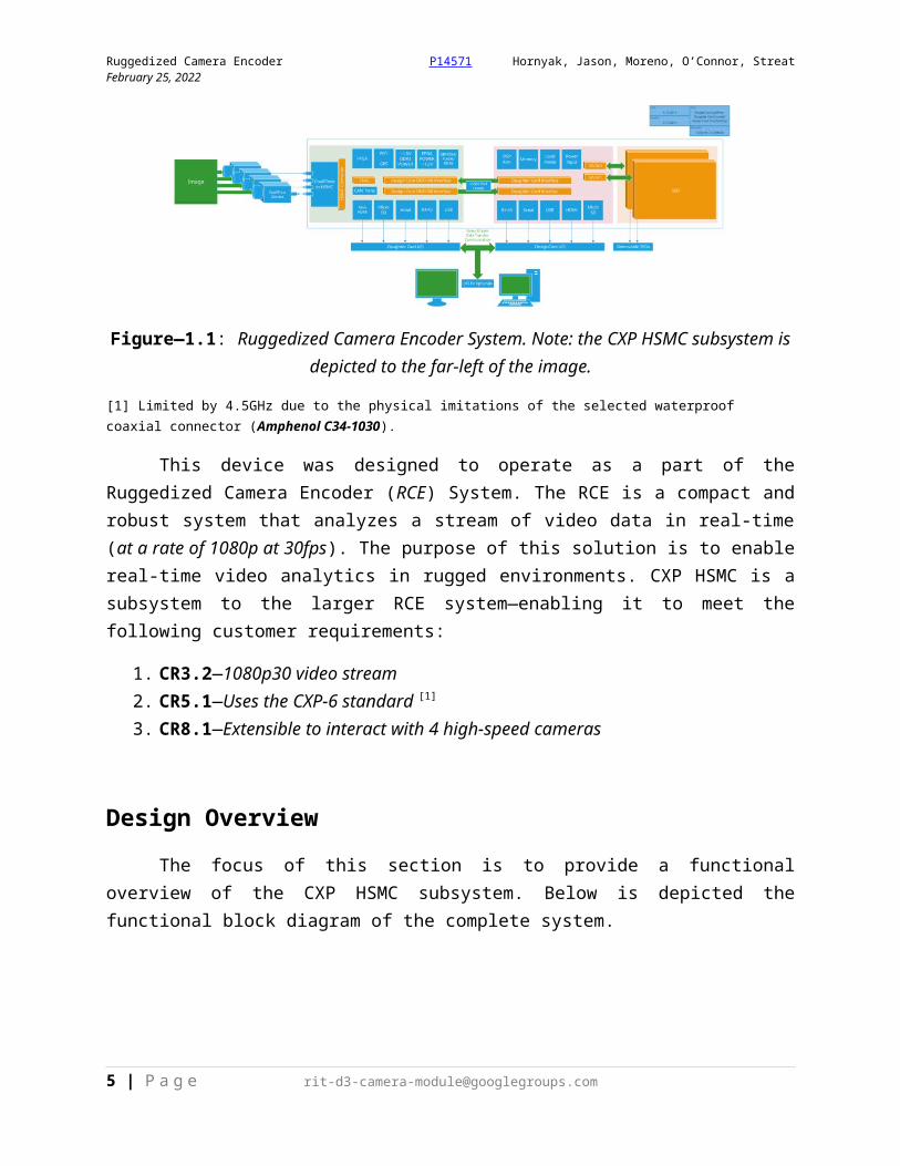
The focus of this section is to provide a functional overview of the CXP HSMC subsystem. Below is depicted the functional block diagram of the complete system.
Figure—1.2: Functional Overview of the CXP HSMC system.
4 | P a g e [email protected]
Ruggedized Camera Encoder P14571 Hornyak, Jason, Moreno, O’Connor, StreatMay 8, 2023
The CXP HSMC system functions as depicted in Figure—1.2:
1. Input is passed into the system via 1-4 cameras.2. Cameras are connected using HD BNC RA BHD connectors (Amphenol 034-1030).
Each camera may use one or more input ports. Multiple ports are used with the aim of increasing data transfer rates (Figure—1.3).
3. The input is received as a serial Current-Mode Logic Signal (CML) and is then converted to a Low Voltage Differential Signal (LVDS) by the EQCO62R20.3 integrated chip—an analog process.
4. The LVDS signal is transported to the host processor via a High Speed Mezzanine Card connector (Samtec ASP-122952-01). Note: Each equalizer will provide a separate LVDS signal—the host processor must implement a driver that properly utilizes the CXP HSMC card’s output. This output must be connected to the transceiver-capable receiver ports.
5. The mezzanine card (hereafter referred to as the CXP HSMC) receives power from the HSMC 12V and 3.3V rails, a DC-DC boost power converter that converts 12V from the host system to 24V (TPS55430) and a buck converter that converts 3.3V to 1.2V (LM3671-1.2). This system meets the power requirements for the CXP HSMC system.
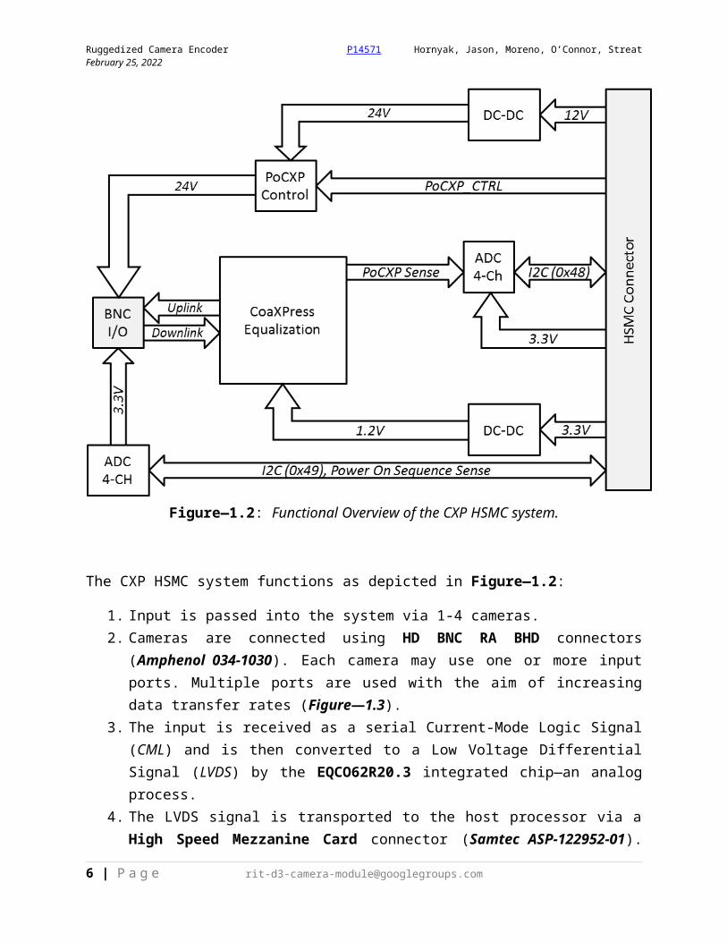
Figure—1.3: Mechanical footprint for the HD BNC RA BHD connectors.
5 | P a g e [email protected]
Ruggedized Camera Encoder P14571 Hornyak, Jason, Moreno, O’Connor, StreatMay 8, 2023
II. Component Functional Descriptions
Overview
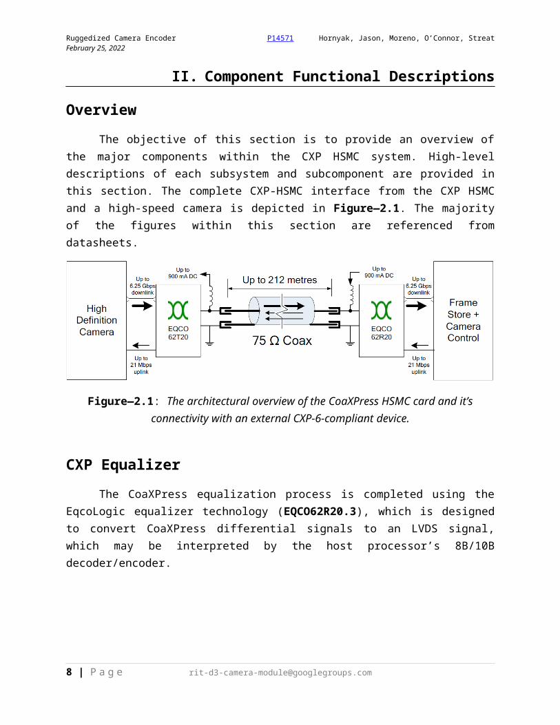
The objective of this section is to provide an overview of the major components within the CXP HSMC system. High-level descriptions of each subsystem and subcomponent are provided in this section. The complete CXP-HSMC interface from the CXP HSMC and a high-speed camera is depicted in Figure—2.1. The majority of the figures within this section are referenced from datasheets.
Figure—2.1: The architectural overview of the CoaXPress HSMC card and it’s connectivity with an external CXP-6-compliant device.
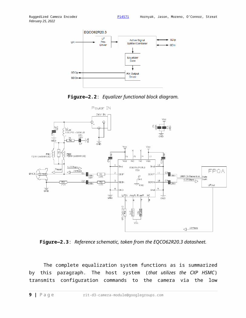
CXP Equalizer
The CoaXPress equalization process is completed using the EqcoLogic equalizer technology (EQCO62R20.3), which is designed to convert CoaXPress differential signals to an LVDS signal, which may be interpreted by the host processor’s 8B/10B decoder/encoder.
Figure—2.2: Equalizer functional block diagram.
6 | P a g e [email protected]
Ruggedized Camera Encoder P14571 Hornyak, Jason, Moreno, O’Connor, StreatMay 8, 2023
Figure—2.3: Reference schematic, taken from the EQCO62R20.3 datasheet.
The complete equalization system functions as is summarized by this paragraph. The host system (that utilizes the CXP HSMC) transmits configuration commands to the camera via the low frequency uplink (LFI—a 1.2V LVTTL signal, which is then stepped up to 2.5V using a series resistor) at a rate of approximately 21Mbs. Through the aid of filtering capacitors and inductors, data and power are transmitted in a bidirectional fashion simultaneously to and from the camera peripheral. The received camera data is acquired on the SDIp
and SDIn input lines. The equalizer core handles the conversion from the low-voltage differential input and then transmits that data back out through the SDOp and SDOn
pins.
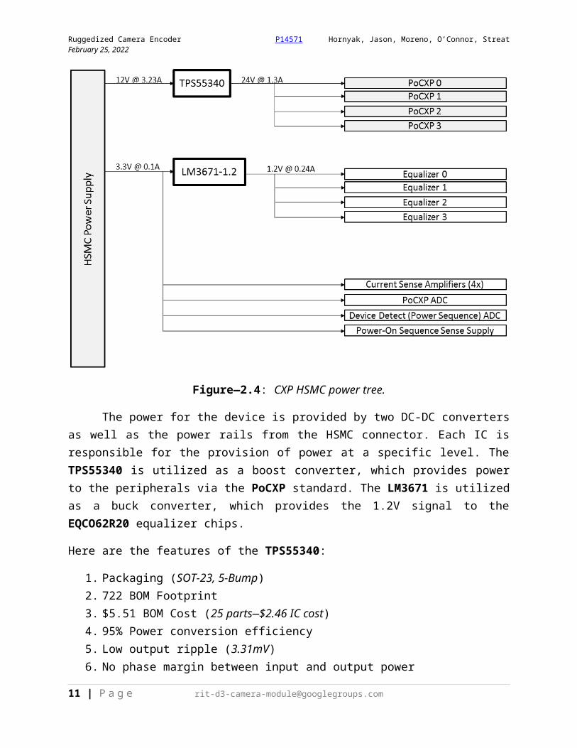
CXP PoCXP Subsystem
This section will depict block diagrams associated with the integrated chips utilized to handle the DC-DC power conversion. For further detail on the power system design, the CXP HSMC Power Design document should be referenced.
7 | P a g e [email protected]
Ruggedized Camera Encoder P14571 Hornyak, Jason, Moreno, O’Connor, StreatMay 8, 2023
Power System: TPS55340, LM371-1.2 & HSMC connector
Figure—2.4: CXP HSMC power tree.
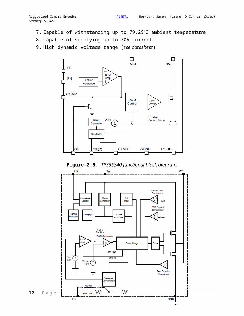
The power for the device is provided by two DC-DC converters as well as the power rails from the HSMC connector. Each IC is responsible for the provision of power at a specific level. The TPS55340 is utilized as a boost converter, which provides power to the peripherals via the PoCXP standard. The LM3671 is utilized as a buck converter, which provides the 1.2V signal to the EQCO62R20 equalizer chips.
Here are the features of the TPS55340:
1. Packaging (SOT-23, 5-Bump)2. 722 BOM Footprint3. $5.51 BOM Cost (25 parts—$2.46 IC cost)4. 95% Power conversion efficiency5. Low output ripple (3.31mV)6. No phase margin between input and output power7. Capable of withstanding up to 79.29oC ambient temperature8. Capable of supplying up to 20A current9. High dynamic voltage range (see datasheet)
8 | P a g e [email protected]
Ruggedized Camera Encoder P14571 Hornyak, Jason, Moreno, O’Connor, StreatMay 8, 2023
Figure—2.5: TPS55340 functional block diagram.
9 | P a g e [email protected]
Ruggedized Camera Encoder P14571 Hornyak, Jason, Moreno, O’Connor, StreatMay 8, 2023
Figure—2.6: LM3671-1.2 functional block diagram.
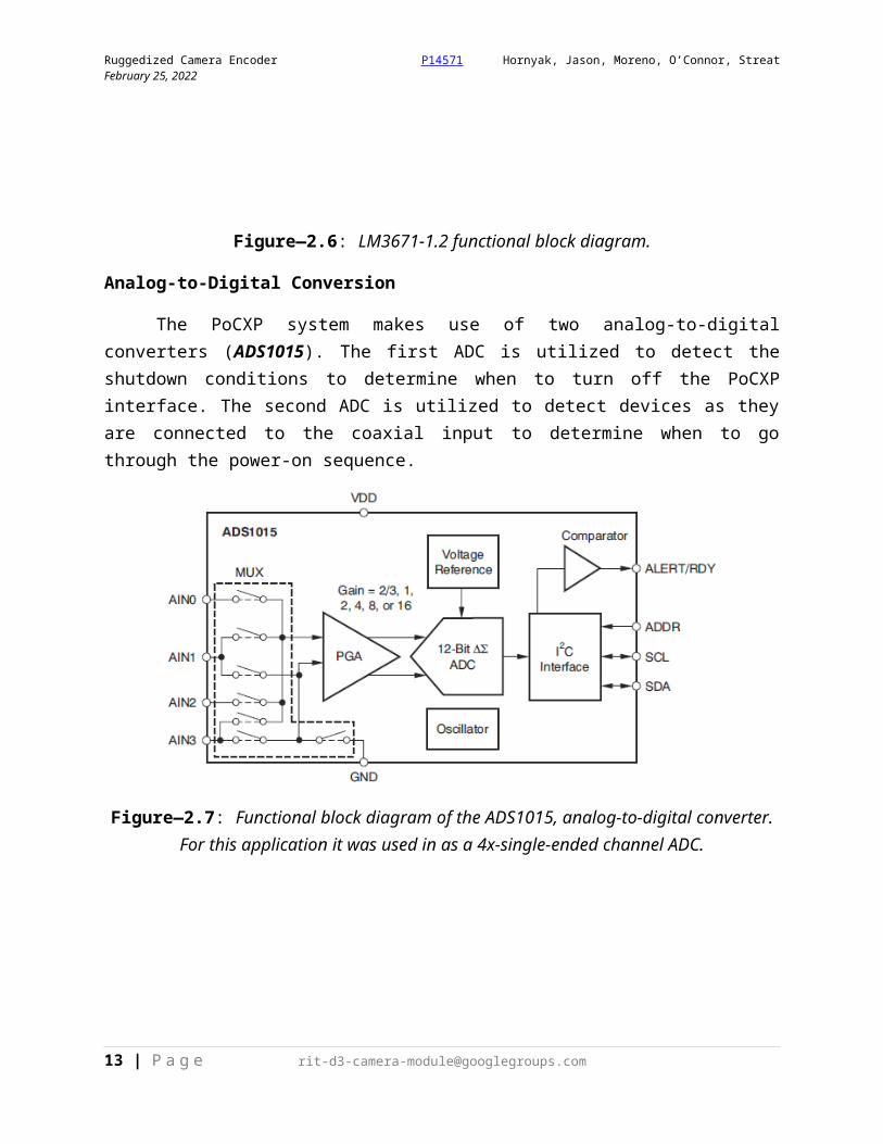
Analog-to-Digital Conversion
The PoCXP system makes use of two analog-to-digital converters (ADS1015). The first ADC is utilized to detect the shutdown conditions to determine when to turn off the PoCXP interface. The second ADC is utilized to detect devices as they are connected to the coaxial input to determine when to go through the power-on sequence.
Figure—2.7: Functional block diagram of the ADS1015, analog-to-digital converter. For this application it was used in as a 4x-single-ended channel ADC.
10 | P a g e [email protected]
Ruggedized Camera Encoder P14571 Hornyak, Jason, Moreno, O’Connor, StreatMay 8, 2023
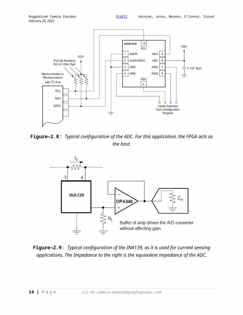
Figure—2.8: Typical configuration of the ADC. For this application, the FPGA acts as the host.
Figure—2.9: Typical configuration of the INA139, as it is used for current sensing applications. The Impedance to the right is the equivalent impedance of the ADC.
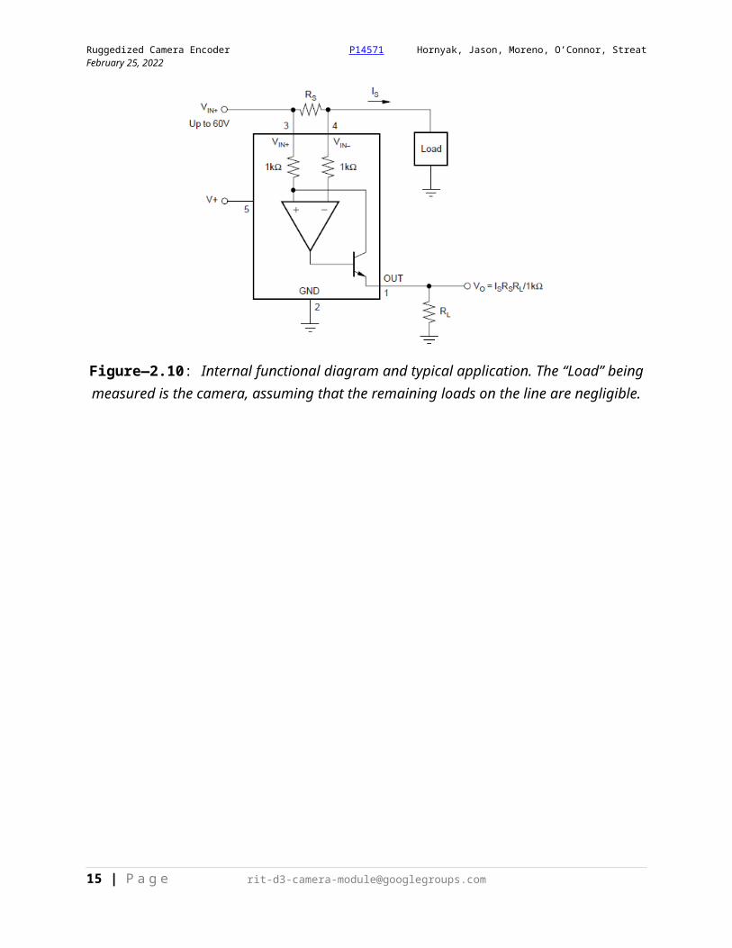
Figure—2.10: Internal functional diagram and typical application. The “Load” being measured is the camera, assuming that the remaining loads on the line are negligible.
11 | P a g e [email protected]
Ruggedized Camera Encoder P14571 Hornyak, Jason, Moreno, O’Connor, StreatMay 8, 2023
III. Specifications
ADC Performance
The conclusions reached in this documentation are based upon information acquired from application notes (cited).
The performance an Analog-to-Digital Converter (ADC) is evaluated based upon various parameters, which are categorized into two groups: static performance parameters and dynamic performance parameters. Static performance parameters are those that are not related to the ADC’s input signal; dynamic performance parameters are associated with the ADC’s input signal—these effects are frequency dependent.
Primary static parameters:
1. Gain error2. Offset error3. Full scale error4. Linearity error
Primary dynamic parameters:
1. Signal-to-noise ratio (SNR)2. Total harmonic distortion (THD)3. Signal-to-noise and distortion (SINAD)4. Effective number of bits (ENOB)
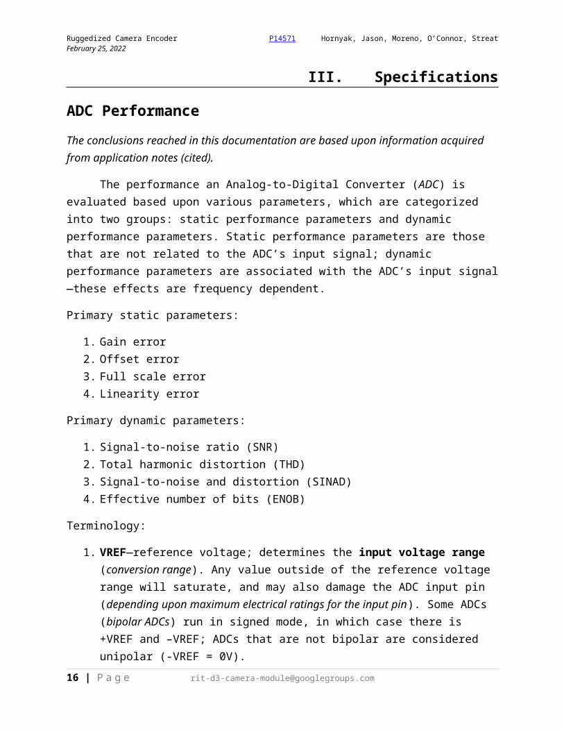
Terminology:
1. VREF—reference voltage; determines the input voltage range (conversion range). Any value outside of the reference voltage range will saturate, and may also damage the ADC input pin (depending upon maximum electrical ratings for the input pin). Some ADCs (bipolar ADCs) run in signed mode, in which case there is +VREF and –VREF; ADCs that are not bipolar are considered unipolar (-VREF = 0V).
2. Resolution—the total number of sub ranges. A sub range represents one LSB, which is the value of VREF divided by the number of bits in the output. This notion of a resolution exists because the ADC quantizes an effectively infinite precision analog value to a finite approximation of that number (represented by some number of bits). Expressed in number of sub ranges or number of bits in output.
3. Conversion mode—describes the manner in which the ADC is configured within the application. Typical modes are: single-ended conversion mode and differential conversion mode.
12 | P a g e [email protected]
Ruggedized Camera Encoder P14571 Hornyak, Jason, Moreno, O’Connor, StreatMay 8, 2023
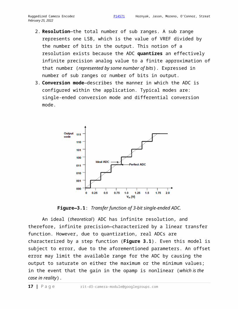
Figure—3.1: Transfer function of 3-bit single-ended ADC.
An ideal (theoretical) ADC has infinite resolution, and therefore, infinite precision—characterized by a linear transfer function. However, due to quantization, real ADCs are characterized by a step function (Figure 3.1). Even this model is subject to error, due to the aforementioned parameters. An offset error may limit the available range for the ADC by causing the output to saturate on either the maximum or the minimum values; in the event that the gain in the opamp is nonlinear (which is the case in reality).
Maximum Ratings
This section contains all of the calculations identifying how the system meets the complete requirements. The conclusions reached in this documentation are based upon information acquired from application notes (cited).
13 | P a g e [email protected]
Ruggedized Camera Encoder P14571 Hornyak, Jason, Moreno, O’Connor, StreatMay 8, 2023
IV. Application Information
CXP HSMC Schematic
Note: For brevity, the schematic has not been included here. However, the reference is provided in a complete datasheet, which also contains a copy of the block diagram and notes explaining the schematic.
Bill of Materials
Note: For brevity, this section has not been included here. Reference the full CXP HSMC Bill of Materials document.
PCB Layout
Note: This section is still in process of being completed.
HSMC Interface
The HSMC specification (owned by Altera) defines the electrical and mechanical properties of high-speed mezzanine card adapters for FPGA-based host processors. The purpose of this standard is to enable interprocessor communication and high speed data transfer. This design is based on the Samtec 0.5 mm pitch, surface-mount QTH/QSH connector family. The connector is separated into three banks—each having a separate clocking mechanism (CLKINx/CLKOUTx), data pins and special functionality. This section is a summary of the requirements found in the published documentation.
HSMC may come in various sizes, but must adhere to the standardized dimensional envelopes. The host processor must also provide 12 V DC and 3.3 V DC to the mezzanine card. The mezzanine card must feature a Samtec ASP-122952-01 connector, which pairs with the Samtec ASP-122953-01 host board connector. The socket is comprised of 160 total pins, and 12 ground plane connection pins in the center. Bank 1 has 40 pins; banks 2 and 3 have 60 pins. Note: the host board
14 | P a g e [email protected]
Ruggedized Camera Encoder P14571 Hornyak, Jason, Moreno, O’Connor, StreatMay 8, 2023
provides transceivers to bank 1 and single-ended signals to banks 2 and 3—the single-ended signals are capable of differential signaling (such as LVDS).
Pins of prime importance on the HSMC port include: pin 1 (XCVR_TXp0), pin 3 (XCVR_TXn0), pin 2 (XCVR_RXp0), and pin 4 (XCVR_RX_n0). The receive signals must also be terminated by 100-Ohms differential; termination should be handled on-die, but board-level termination is acceptable. Trace widths must be 5 mm or greater to reduce skin-effect losses and should reference the ground layer with no split plane crossings. Signal traces should not run more than 8 in on the host or the mezzanine card. The purposes of these specifications are to promote signal integrity. Traces should be simulated if they are designed to run faster than 1Gbs.
Ideally, the FPGA should be capable of providing 50-Ohm output impedances for its driving signal. Bi-directional capabilities must be available on all CMOS class pins. When connected to the HSMC port, the mezzanine card’s load should cause the host processor to light indicate a proper mechanical connection via a PSTn LED. Voltage and current specifications must be met. Traces containing the LVDS or CMOS signals should be closer to their reference plane than they are to each other and should meet specific length requirements.
Figure—4.1: Cut out underneath Surface Mount Device (SMD) pads
Limited cross-talk is allowed (10% of the signal swing). For example, a 3.3V source should not result in a swing greater than 330mV in any other data line. To ensure this, parallelism rules must be followed during the design phase. The documentation also specifies the recommended wire relative distances for parallel traces that minimizes cross talk to a safe threshold. The host processor must provide the mezzanine card with 1 Amp for 12 V lines and 2 Amps for 3.3 V lines. The complete HSMC is allotted 18.6 W at a minimum. Cabling within specification is available.
Impedance fluctuation should be closely considered—one technique that is used to adjust the impedance at the connector pads is executed by making cut outs on the plane of the layer just below the SMT pad. Sample pad structure is provided in Fig. 2.1b.
15 | P a g e [email protected]
Ruggedized Camera Encoder P14571 Hornyak, Jason, Moreno, O’Connor, StreatMay 8, 2023
Summary of used HSMC pin usage:
1. Eqcologic Chip #0a. XCVR_RXp0 (pin 30)b. XCVR_RXn0 (pin 32)c. EQCO0_ULINK (pin 41)d. EQCO0_PoCXP_CTRL (pin 47)
2. Eqcologic Chip #1a. XCVR_RXp1 (pin 26)b. XCVR_RXn1 (pin 28)c. EQCO1_ULINK (pin 42)d. EQCO0_PoCXP_CTRL (pin 48)
3. Eqcologic Chip #2a. XCVR_RXp2 (pin 22)b. XCVR_RXn2 (pin 24)c. EQCO2_ULINK (pin 43)d. EQCO0_PoCXP_CTRL (pin 49)
4. Eqcologic Chip #3a. XCVR_RXp3 (pin 18)b. XCVR_RXn3 (pin 20)c. EQCO3_ULINK (pin 44)d. EQCO0_PoCXP_CTRL (pin 50)
5. 12V Supply Rail (pins 46, 52, 58, 64, 70, 76, 82, 88, 94, 100, 106, 112, 118, 124, 130, 136, 142, 148, and 154)
6. I2C Interfacea. SDA (pin 53)b. SCL (pin 55)
Test Plan
Note: For brevity, this section has not been included here. Reference the full CoaXPress HSMC Test Plan document.
16 | P a g e [email protected]
Ruggedized Camera Encoder P14571 Hornyak, Jason, Moreno, O’Connor, StreatMay 8, 2023
V. Conclusion
Feasibility
The CXP interface is completely a feasible design. However, the primary risks concerning this design are significant. There are many different factors that needed to be considered with regards to the actual design. These are brought into light in the Test Plan document.
References
Note: Section not completed, yet non-essential.
Notes:
17 | P a g e [email protected]


![Features...1,R 2, 3 = internal resistors [Ω] Rup Trim +Sense-Sense Trim Rdown Positve Logic DC-DC ON DC-DC OFF Open or 3.0VDC < V CTRL < 12VDC Short or 0VDC < V CTRL < 1…](https://img.pdfslide.net/doc/110x75/60c1f64ea1b3125bce622c56/features-1r-2-3-internal-resistors-rup-trim-sense-sense-trim-rdown.jpg)