Embed Size (px)
Citation preview

1/27/2010
1
EE‐110 – Basic Electronics
Lecture #2
Diodes
Subtopics1.0 Semiconductor diodes (3 hours)
1.1 Introduction to semiconductors materials
1.2 Introduction to diode1.2 Introduction to diode
1.3 Introduction to Zener diode and LED
2.0 Diode applications ( 6 hours)2.1 Load line analysis and diode approximation
2.2 Series‐Parallel Configuration
2.3 Half‐wave and Full‐wave rectification
2.4 Clippers and Clampers
2.5 Zener diode application

1/27/2010
2
Early Diodes• Thermionic diodes are thermionic valve devices (also known as vacuum tubes)
• Electrodes surrounded by a vacuum within a glass envelope, similar in appearance to incandescent light bulbs.
Semiconductor Diodes• Most modern diodes are based on semiconductor p‐n junctionssemiconductor p n junctions
• In a p‐n diode, conventional current can flow from the p‐type side (the anode) to the n‐type side (the cathode), but cannot flow in the opposite direction.
Diode symbol

1/27/2010
3
Semiconductor Diodes• Comparison of Ge, Si and GaAs diodes
Zener region
Zener Diode• A special type of diode that is supposed to be reversed biased
• Zener diode works in zener region where theZener diode works in zener region where the diode start to breakdown at breakdown avalanche voltage (VZ), and the current is avalanche current (IZ)
• It limits a voltage to a certain point to pass through the zener diode

1/27/2010
4
Zener Diode
LED (Light‐Emitting Diode)
• In a forward‐biased p‐n junction, recombination of the holes and electrons requires energy
d b h b d f lpossessed by the unbound free electrons
• In Si and Ge, most of the energy is dissipated in the form of heat and photons
• But in other material such as GaAs, the energy generate light but it is invisible for the eye togenerate light but it is invisible for the eye to see (infrared)
• Other materials that emit light during forward‐bias operation

1/27/2010
5
LED (Light‐Emitting Diode)Color Construction Forward
VoltageAmberBlueGreenOrange
AlInGaPGaNGaP
GaAsP
2.15.02.22.0
Red WhiteYellow
GaAsPGaN
AlInGaP
1.84.12.1
LED (Light‐Emitting Diode)
• How an LED works
1/27/2010
6
Diode Approximation
• Diode equivalent circuits:– Ideal Equivalent Circuit
– Simplified Equivalent Circuit
– Piecewise‐Linear Equivalent Circuit
• Purpose: to represent diode
Piecewise‐Linear Equivalent Circuit• Approximation representation of the actual diode
• Diode have VD and rav for the slope regionDiode have VD and rav for the slope region
1/27/2010
7
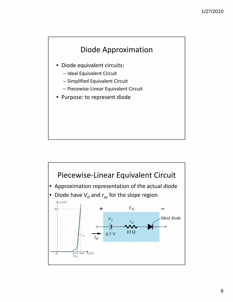
Simplified Equivalent Circuit
• Assume straight vertical line of ID at VD
• No rav
Ideal Equivalent Circuit
• Diode as an ideal switch
• No VD or rav

1/27/2010
8
Load‐Line Analysis• A simple analysis which used the diode characteristic to obtain the Q‐point (operation
i )point)
• A series diode circuit and characteristic:
Load‐Line Analysis
• IVVVE +=+=•• For
• For
• Connect a line between E / R and E
• The overlap of the lines becomes the Q
RDRD IVVVE +=+=
REIRIRIEV DDDD =∴=+== ,0 ,0
EVVRVEI DDDD =∴=+== ,)0( ,0
• The overlap of the lines becomes the Q‐point of the diode and IDQ and VDQ will be obtained

1/27/2010
9
Load‐Line Analysis
Problem 2.1a
• Determine ID, VD & VR
• The circuit:

1/27/2010
10
Problem 2.1a• The diode characteristic:
Problem 2.1a
• Solution:– The circuit representation:
– For
– For
RIVVVE DDRD +=+=
mA 24.2433.080 ,0
===∴
+==
kREI
RIEV
D
DD
For
V 8)0( ,0
==∴+==
EVRVEI
D
DD
1/27/2010
11
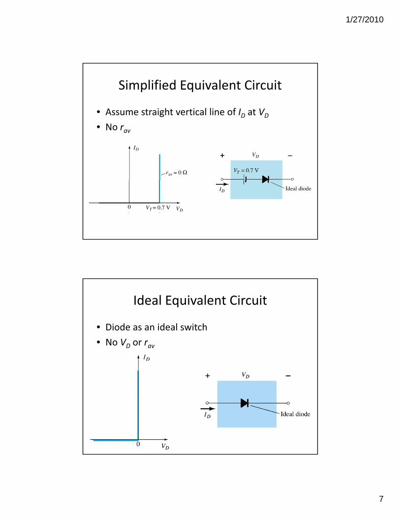
Problem 2.1a• The load‐line analysis becomes:
RE
Q-point
DQI
E
DQV
Problem 2.1a
• From the analysis:– VDQ = VD ≈ 0.9 V
– IDQ = ID ≈ 21.5 mA
– For VR
)33.0)(5.21(==
kmRIV DR
V 095.7)33.0)(5.21(
=km

1/27/2010
12
Problem 2.1b• Re‐do Problem 2.1a using approximate (simplified) model for diode and compare the result
• The diode characteristic becomes:
Problem 2.1b
• The solution:

1/27/2010
13
Problem 2.1b• VD is always 0.7 V, so VD = VDQ = 0.7 V
• From the graph, IDQ = ID ≈ 22 mAg p ,
• So, we get VR = (22m)(0.33k) = 7.26 V ≈ 7.3 V
• Using Kirchoff’s voltage law, E = VD + VR
V377.08=∴+= R
VV
• The answer are the sameV3.7=∴ RV
Problem 2.1c• Re‐do Problem 2.1a using ideal model for diode and compare the result
• The diode characteristic becomes:

1/27/2010
14
Problem 2.1c• The solution
Problem 2.1c
• VD is always 0 V, so VD = VDQ = 0 V
• It acts like an ideal switch
• From the graph, IDQ = ID ≈ 24.24 mA
• So, we get VR = (24.24m)(0.33k) = 7.9992 V ≈ 8 V
• Using Kirchoff’s voltage law, E = VR
• The answer are the same
V 8=∴ RV

1/27/2010
15
Series‐Parallel Configuration
• Diode can be applied to any circuits
U ll di d i d• Usually diode is represented as an approximated (simplified) model diode
• To keep the calculation simple, just use the Kirchoff’s voltage & current law
• Hint: it is easier to use nodal analysis• Hint: it is easier to use nodal analysis technique for circuit representation
• Important: strong knowledge in CIRCUIT THEORY!!!!!
Problem 2.5a
• Find I
• The circuit:

1/27/2010
16
Problem 2.5a
• For Si, VD = 0.7 V
• Notice that the diode is in reverse‐bias configuration
• So, no current will flow, I = 0 A
Problem 2.5b
• Find I
• The circuit:

1/27/2010
17
Problem 2.5bSolution:
• Using nodal analysis, node V is equal to the g y , qvoltage supplied, so V = 20
V
Problem 2.5b
• Using the simple Ohm’s law:
A 965.020
7.020=
−==
RVI

1/27/2010
18
Problem 2.5c
• Find I
• The circuit:
Problem 2.5cSolution:
• One of the diode is in reverse‐bias resulting in gopen circuit for that part

1/27/2010
19
Problem 2.5c
So, by using the simple Ohm’s law:
A110===
VI A110R
I
Problem 2.7a
• Find Vo• The circuit:

1/27/2010
20
Problem 2.7a• Both the diode are in forward‐bias, so both are short‐circuited
• For Si, VD = 0.7 V
• For Ge, VD = 0.3 V
• The circuit becomes:
0.7 V 0.3 V
SIMPLIFIED
19 V
Problem 2.7a
Solution:
• Using nodal analysis, voltage at Vo:
2219 00 =
−k
VkV
V 5.922
0 =∴Vkk

1/27/2010
21
Problem 2.7b
• Find Vo• The circuit:
Problem 2.7b
• The circuit becomes:
0.7 V

1/27/2010
22
Problem 2.7b
Solution:
• The nodal analysis of node Vo:
74)2(
217.010 00 −−
=−−
kV
kV
V 77.42.1
0 =∴Vkk
Problem 2.11a
• Find Vo & I:
• The circuit:

1/27/2010
23
Problem 2.11a• For Si, VD = 0.7 V
• For Ge, VD = 0.3 VFor Ge, VD 0.3 V
• Because of this, current will flow in the Ge’sdiode route
• Naturally, current will
0.3 V
select the easiest/fastest route
• So, the circuit becomes:
Problem 2.11a
Solution:
• Using Kirchoff’s voltage law:
• For I, by using basic Ohm’s law:
V 7.93.0100 =−=V
mA 7.91
7.90 ===kR
VI

1/27/2010
24
Problem 2.11b
• Find Vo & I:
• The circuit:
Problem 2.11b
• For the same type of di d th i it illdiode, the circuit will becomes:
• Because there is no resistor exist in the parallel route of the
0.7 V0.7 V
0.7 V
pdiode, current will flow in only one of the diode’s route

1/27/2010
25
Problem 2.11b
Solution:
• Using Kirchoff’s voltage law:
• For I, by using Ohm’s law:
V 6.147.07.0160 =−−=V
mA 553.07.4
126.14=
−=
kI
Problem 2.13
• Find Vo & ID• The circuit:

1/27/2010
26
Problem 2.13
• The circuit becomes:
0.7 V
0.7 V
9.3 V
SIMPLIFIED 9.3 V
SIMPLIFIED
Problem 2.13
Solution:
• The nodal analysis for node Vo:
V 2.621
3.9
0
00
=∴
=−
Vk
Vk
V
• For ID: mA 55.12
2.63.9=
−=
kID

1/27/2010
27
Rectification
• Rectify means improvement, cure healing ( b ik b hb ik )(pembaikan, penambahbaikan)
• For a sinusoidal waveform or any supply that has a variation of input value, diode can be used for rectification
• Rectification are used to modified the inputRectification are used to modified the input value to become only the signal that we want
Half‐Wave Rectification
• For a full cycle of a sinusoidal or continuous waveform only half of the waveform is takenwaveform, only half of the waveform is taken to be rectified

1/27/2010
28
Half‐Wave Rectification• For the period 0 T/2, the sinusoidal input will give a forward bias supply to the circuit
• The diode will “on” and current will pass through
• Assume that the diode is ideal
Half‐Wave Rectification• For the period T/2 T, the sinusoidal input will give a reverse bias supply to the circuit
• The diode will “off” and no current can pass through
• Assume that the diode is ideal

1/27/2010
29
Half‐Wave Rectification
• For a continuous i di fperiodic waveform,
the rectified waveform will become:
• Where as:
mdc VV 318.0=
Problem 2.25
• Sketch Vo and determine Vdc:

1/27/2010
30
Problem 2.25
Solution:
• To obtain Vm from Vrms:
• The output Vo will be:V 56.155)110(2
2
==
= rmsm VV
• Vdc will be:V 47.49)56.155(318.0
318.0==
= mdc VV
Problem 2.26
• Sketch Vo

1/27/2010
31
Problem 2.26
• Solution:
F th iti i t• For the positive input supply:
• The circuit becomes:
• For Vi < 0.7V:For Vi ≥ 0 7V:For Vi ≥ 0.7V:
0.7 V
Problem 2.26
• The output for the positive input supply bbecomes:
• For the negative input supply:

1/27/2010
32
Problem 2.26
• The circuit becomes:
• For maximum Vo: The output becomes:
VVk
Vk
V
o 091.9101
10 00
−=∴
=−−
+
-
Problem 2.26
• Combine both the output becomes:

1/27/2010
33
PIV or PRV
• Peak Inverse Voltage (PIV) or Peak Reverse V lt (PRV)Voltage (PRV)
• It is a rating to make sure for the reverse‐bias operation, the diode didn’t enter the Zenerregion
• PIV is set according to the circuit and the inputPIV is set according to the circuit and the input voltage
mV rating PIV ≥for half-wave rectifier
Full‐Wave Rectification
• The whole cycle of input signal is used and tifi drectified
• Two commonly types of full‐wave rectifier:– Bridge Network
– Center‐Tapped (CT) Transformer
• The dc level from a sinusoidal input can be• The dc level from a sinusoidal input can be improved 100%. So the Vdc becomes:
mdc VV 636.0=

1/27/2010
34
Full‐Wave Rectifier: Bridge Network
• The most commonly bridge network fi ti b ild ith 4 di dconfiguration are build with 4 diodes
Full‐Wave Rectifier: Bridge Network
• For the positive input supply, the current will t k th t h b l d thtake the route as shown below, and the output will becomes:
1/27/2010
35
Full‐Wave Rectifier: Bridge Network
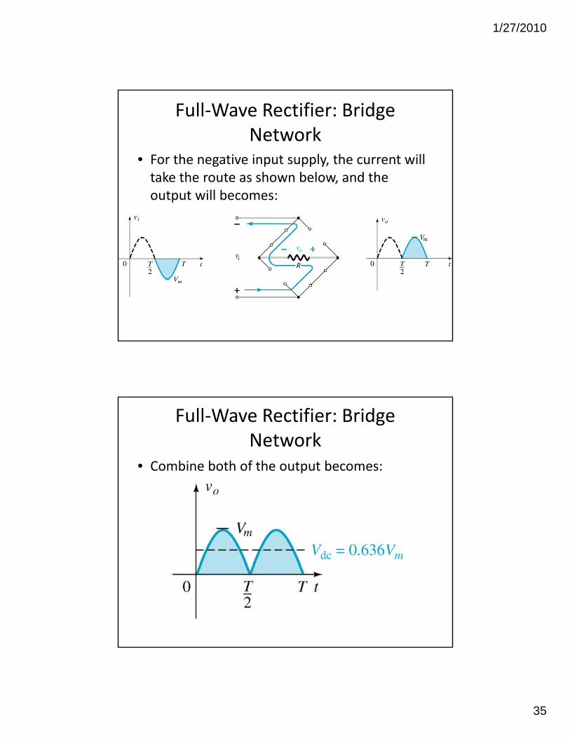
• For the negative input supply, the current will t k th t h b l d thtake the route as shown below, and the output will becomes:
Full‐Wave Rectifier: Bridge Network
• Combine both of the output becomes:

1/27/2010
36
Full‐Wave Rectifier: Bridge Network
• Due to the maximum voltage from the input l i V t k th di d f thsupply is Vm, to keep the diode away from the
Zener region, the PIV rating is:
mV rating PIV ≥ mfor full-wave rectifier: bridge network
Full‐Wave Rectifier: Center‐Tapped (CT) Transformer
• It is constructed with 2 diodes and a center‐tapped transformertapped transformer
• The transformer ratio is 1:2

1/27/2010
37
Full‐Wave Rectifier: Center‐Tapped (CT) Transformer
• For the positive input supply:
Full‐Wave Rectifier: Center‐Tapped (CT) Transformer
• For the negative input supply:

1/27/2010
38
Problem 2.28
• The circuit:All diodes are silicon
120 Vrms
All diodes are silicon
1 kΩ