Embed Size (px)
Citation preview

EE 330
Lecture 41
Digital Circuits
• Propagation Delay With Multiple Levels of Logic
• Optimally driving large capacitive loads
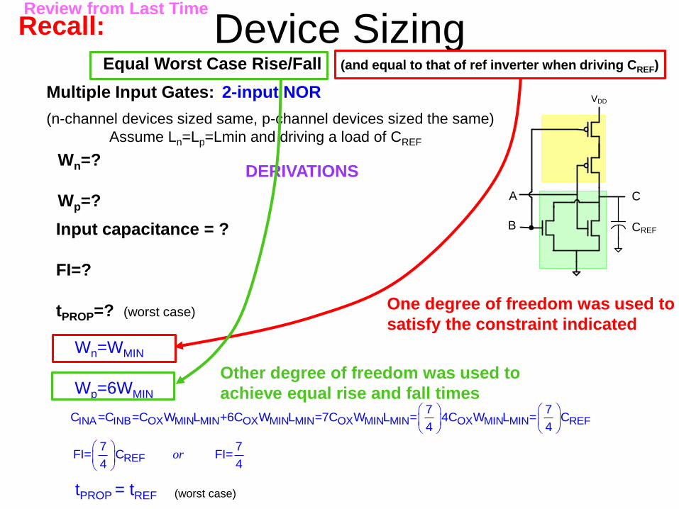
Device Sizing
Multiple Input Gates: 2-input NOR
DERIVATIONSWn=?
Wp=?
Equal Worst Case Rise/Fall (and equal to that of ref inverter when driving CREF)
Input capacitance = ?
FI=?
tPROP=? (worst case)
(n-channel devices sized same, p-channel devices sized the same)
Assume Ln=Lp=Lmin and driving a load of CREF
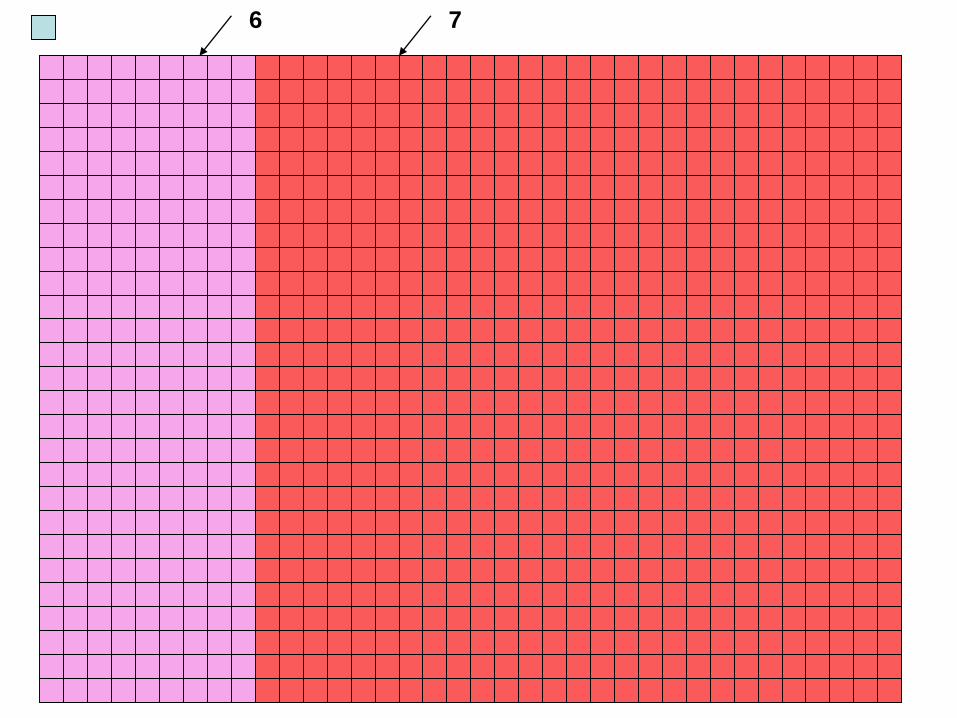
A
B
C
VDD
CREF
Wn=WMIN
Wp=6WMIN
INA INB OX MIN MIN OX MIN MIN OX MIN MIN OX MIN MIN REF7 7
C =C =C W L +6C W L =7C W L = 4C W L = C4 4
REF7 7
FI= C FI=4 4
or
tPROP = tREF (worst case)
Recall:
One degree of freedom was used to
satisfy the constraint indicated
Other degree of freedom was used to
achieve equal rise and fall times
Review from Last Time
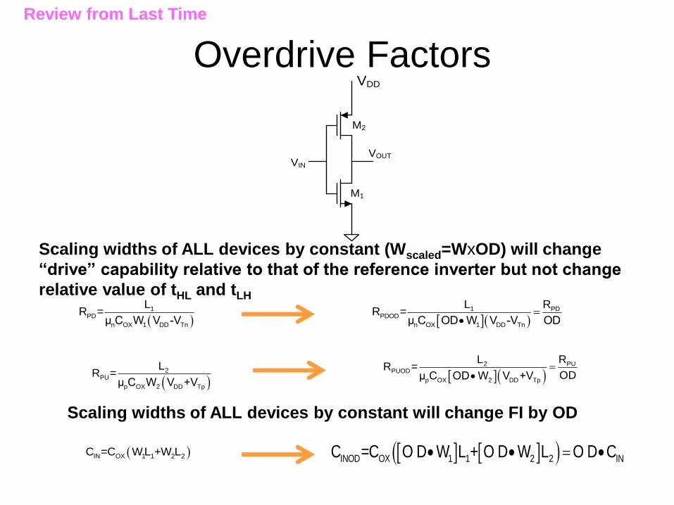
Overdrive Factors
VIN
VOUT
M1
M2
VDD
Scaling widths of ALL devices by constant (Wscaled=WxOD) will change
“drive” capability relative to that of the reference inverter but not change
relative value of tHL and tLH
1
PD
n OX 1 DD Tn
LR =
μ C W V -V 1 PD
PDOD
n OX 1 DD Tn
L RR =
μ C OD W V -V OD
IN OX 1 1 2 2C =C WL +W L
PU2
PUOD
p OX 2 DD Tp
RLR =
ODμ C OD W V +V
Scaling widths of ALL devices by constant will change FI by OD
2
PU
p OX 2 DD Tp
LR =
μ C W V +V
INOD OX 1 1 2 2 INC =C O D W L + O D W L O D C
Review from Last Time
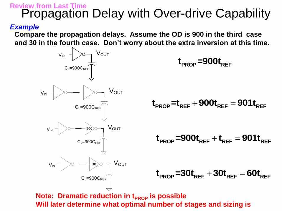
Propagation Delay with Over-drive Capability
CL=900CREF
VINVOUT
Example
CL=900CREF
VINVOUT900
CL=900CREF
VINVOUT30
Compare the propagation delays. Assume the OD is 900 in the third case
and 30 in the fourth case. Don’t worry about the extra inversion at this time.
PROP REF REF REFt =t 900t 901t
PROP REF REF REFt =900t t 901t
PROP REF REF REFt =30t 30t 60t
Note: Dramatic reduction in tPROP is possible
Will later determine what optimal number of stages and sizing is
CL=900CREF
VINVOUT
PROP REFt =900t
Review from Last Time
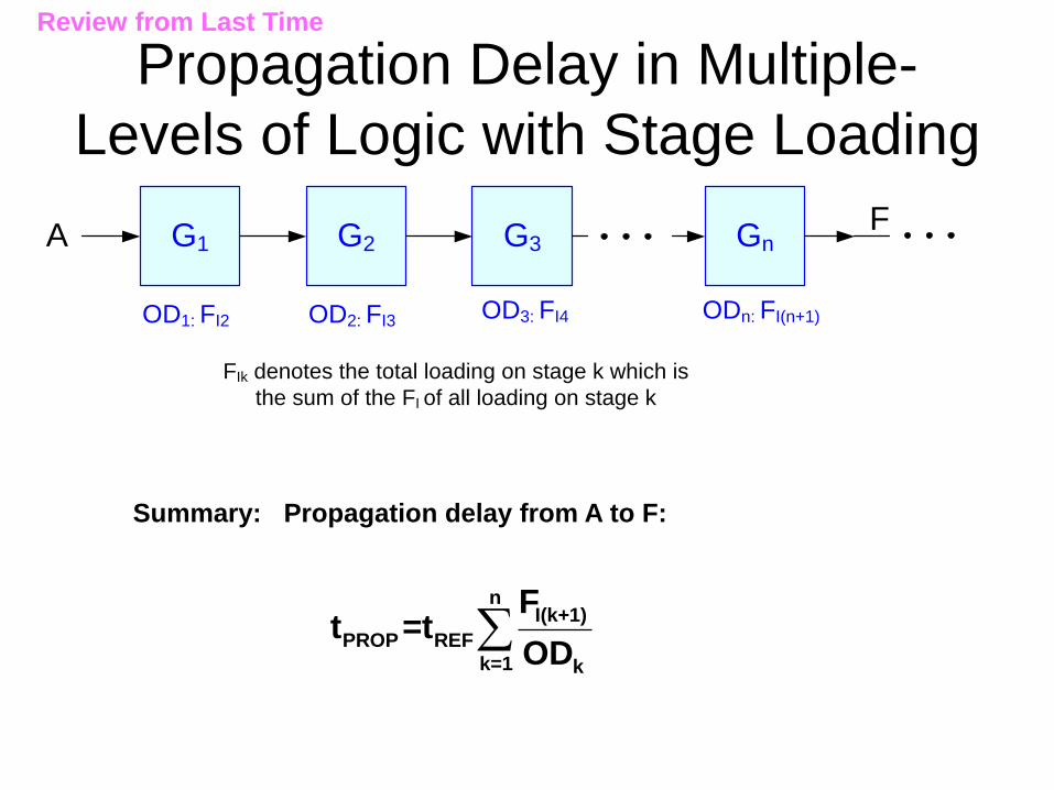
Propagation Delay in Multiple-
Levels of Logic with Stage Loading
G1 G2 G3 GnAF
OD1: FI2 OD2: FI3 OD3: FI4 ODn: FI(n+1)
FIk denotes the total loading on stage k which is
the sum of the FI of all loading on stage k
Summary: Propagation delay from A to F:
nI(k+1)
PROP REF
k=1 k
Ft =t
OD
Review from Last Time
Propagation Delay in Multiple-
Levels of Logic with Stage Loading
• Equal rise/fall (no overdrive)
• Equal rise/fall with overdrive
• Minimum Sized
• Asymmetric Overdrive
• Combination of equal rise/fall,
minimum size and overdrive
Will consider an example with the five cases
Will develop the analysis methods as needed
Review from Last Time
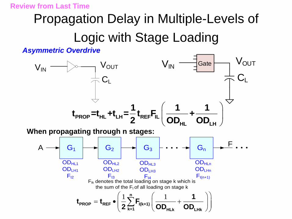
Propagation Delay in Multiple-Levels of
Logic with Stage Loading
CL
VINVOUT
PROP HL LH REF IL
HL LH
1 1 1t =t +t = t F +
2 OD OD
Asymmetric Overdrive
G1 G2 G3 GnAF
ODHL1
ODLH1
FI2
FIk denotes the total loading on stage k which is
the sum of the FI of all loading on stage k
ODHL2
ODLH2
FI3
ODHL3
ODLH3
FI4
ODHLn
ODLHn
FI(n+1)
When propagating through n stages:
1 1
n
PROP REF I(k+1)
k=1 HLk LHk
1t t F
2 OD OD
CL
VINVOUTGate
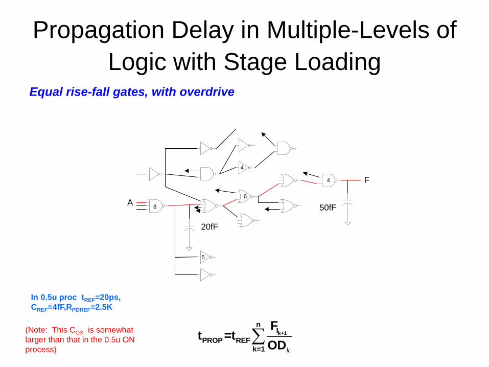
Review from Last Time
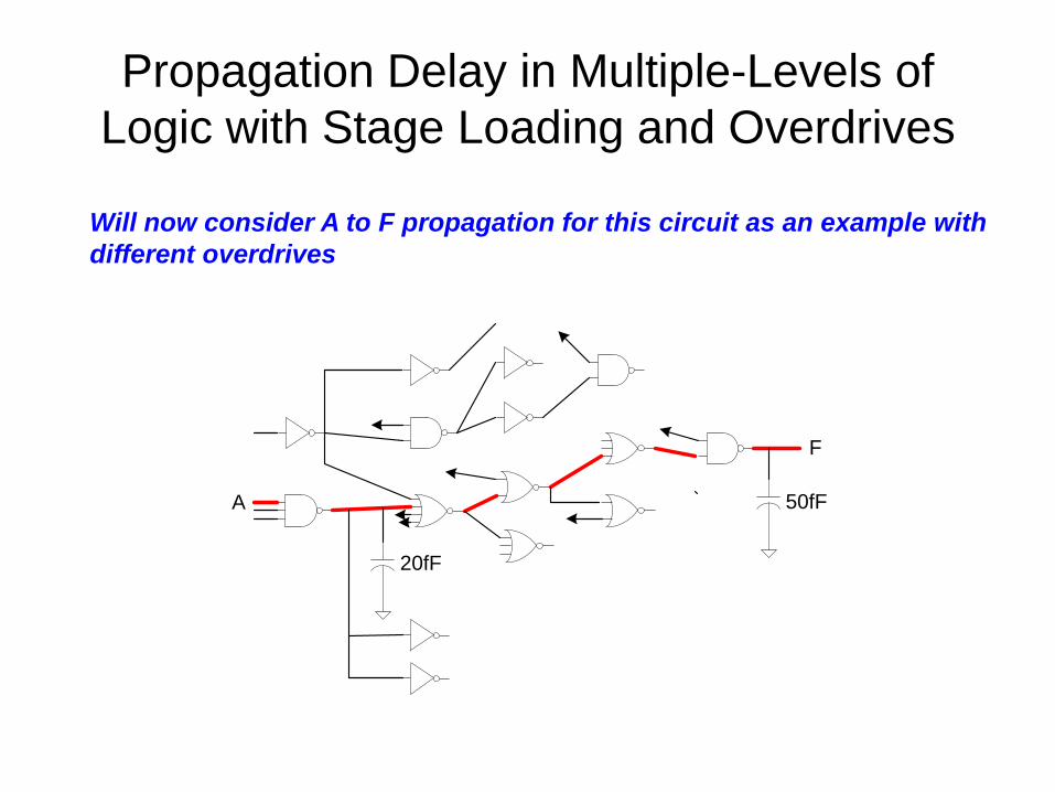
Propagation Delay in Multiple-Levels of
Logic with Stage Loading and Overdrives
A
F
50fF
20fF
Will now consider A to F propagation for this circuit as an example with
different overdrives
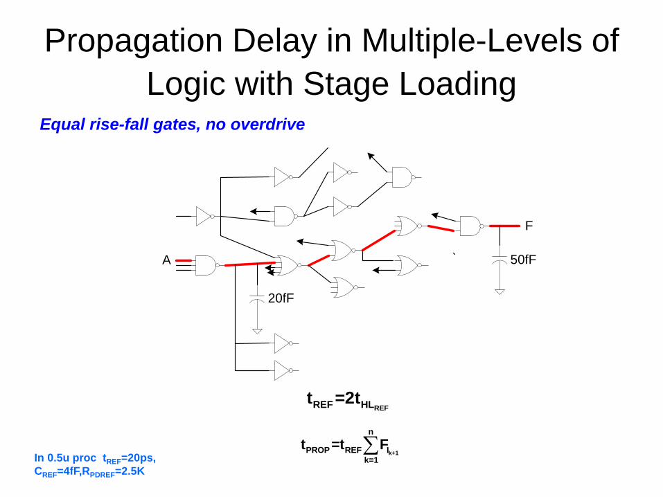
Propagation Delay in Multiple-Levels of
Logic with Stage Loading
A
F
50fF
20fF
REFREF HLt =2t
k+1
n
PROP REF I
k=1
t =t F
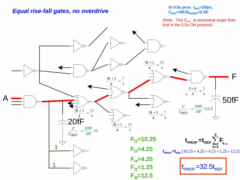
Equal rise-fall gates, no overdrive
In 0.5u proc tREF=20ps,
CREF=4fF,RPDREF=2.5K
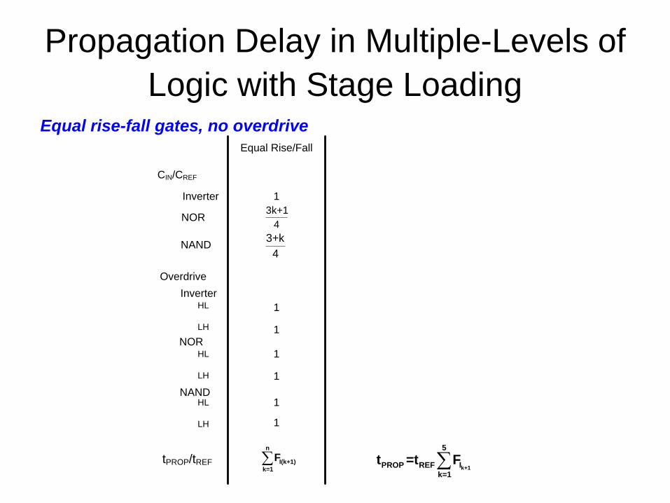
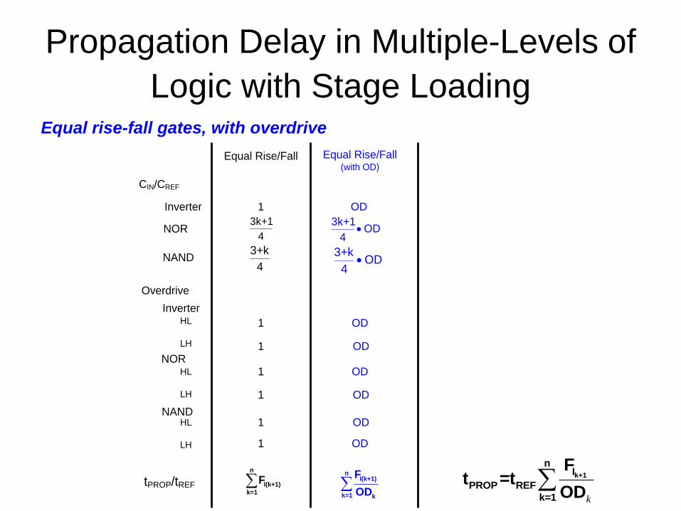
Propagation Delay in Multiple-Levels of
Logic with Stage LoadingEqual rise-fall gates, no overdrive
CIN/CREF
Equal Rise/Fall
Inverter
NAND
NOR
1
3k+1
4
3+k
4
Overdrive
HL
LH
1
1NOR
NAND
Inverter
HL
LH
HL
LH
1
1
1
1
n
I(k+1)
k=1
FtPROP/tREF k+1
5
PROP REF I
k=1
t =t F
A
F
50fF
20fF
k+1
5
PROP REF I
k=1
t =t F
Equal rise-fall gates, no overdrive
3 1
4
13
4
k
3 1
4
10
4
k
3 7
4
1
4
k
3 1
4
10
4
k
3 7
4
1
4
k
3 5
44
k
In 0.5u proc tREF=20ps,
CREF=4fF,RPDREF=2.5K
20fF=5
4fFREF
C
C
50fF=12.5
4fFREF
C
C
1
1
FI2=10.25
FI3=4.25
FI4=4.25
FI5=1.25
FI6=12.5
10.25 4.25 4.25 1.25 12.5 PROP REFt =t
PROP REFt =32.5t
(Note: This COX is somewhat larger than
that in the 0.5u ON process)
Propagation Delay in Multiple-Levels of
Logic with Stage Loading
A
F4
4
6
8
20fF
50fF
5
Equal rise-fall gates, with overdrive
k+1
nI
PROP REF
k=1
Ft =t
ODk
In 0.5u proc tREF=20ps,
CREF=4fF,RPDREF=2.5K
(Note: This COX is somewhat
larger than that in the 0.5u ON
process)
Propagation Delay in Multiple-Levels of
Logic with Stage LoadingEqual rise-fall gates, with overdrive
k+1
nI
PROP REF
k=1
Ft =t
ODk
CIN/CREF
Equal Rise/Fall
Inverter
NAND
NOR
1
3k+1
4
3+k
4
Overdrive
HL
LH
1
1NOR
NAND
Inverter
HL
LH
HL
LH
1
1
1
1
Equal Rise/Fall(with OD)
OD
3k+1OD
4
3+kOD
4
OD
OD
OD
OD
OD
OD
n
I(k+1)
k=1 k
F
OD
n
I(k+1)
k=1
FtPROP/tREF
A
F4
4
6
8
20fF
50fF
5
Equal rise-fall gates, with overdrive
k+1
nI
PROP REF
k=1
Ft =t
ODk
3 3
4
1
4
1OD
k
20fF=5
4fFREF
C
C
OD 5
1
3 0
4
1
4
1OD
k
3 1
2
1
4
2OD
k
3 1
4
7
4OD
k
3 0
4
1
4
1OD
k
3 0
44
2OD
k
50fF=12.5
4fFREF
C
C
In 0.5u proc tREF=20ps,
CREF=4fF,RPDREF=2.5K
FI2=14.25
FI3=13
FI4=4.25
FI5=5
FI6=12.5
PROP REF
14.25 13 4.25 5 12.5t =t + + + +
8 1 6 1 4
PROP REFt =23.6 t
(Note: This COX is somewhat larger
than that in the 0.5u ON process)
Propagation Delay in Multiple-Levels of
Logic with Stage Loading
A
F
20fF
50fF
?PROP REFt = t
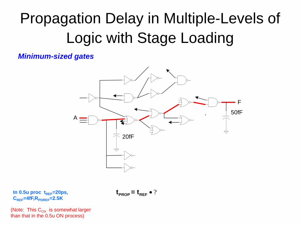
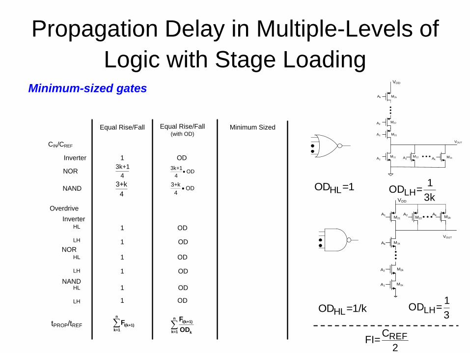
Minimum-sized gates
In 0.5u proc tREF=20ps,
CREF=4fF,RPDREF=2.5K
(Note: This COX is somewhat larger
than that in the 0.5u ON process)
Propagation Delay in Multiple-Levels of
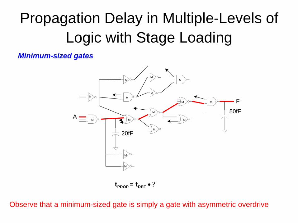
Logic with Stage Loading
A
F
M
M
M
M
M M
M
M
M
M
M
M
M
M
M
20fF
50fF
?PROP REFt = t
Minimum-sized gates
Observe that a minimum-sized gate is simply a gate with asymmetric overdrive
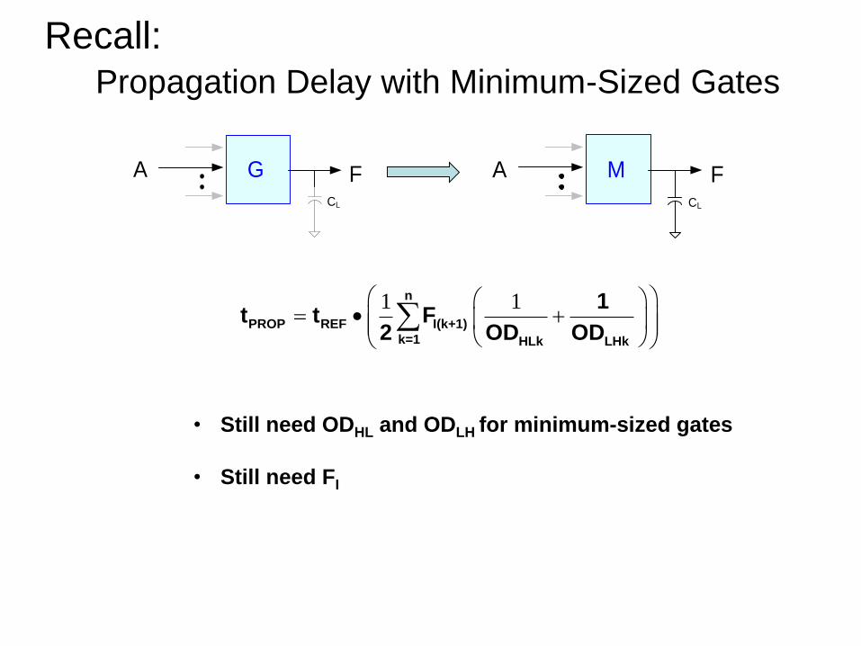
Propagation Delay with Minimum-Sized Gates
GA FCL
1 1
n
PROP REF I(k+1)
k=1 HLk LHk
1t t F
2 OD OD
• Still need ODHL and ODLH for minimum-sized gates
• Still need FI
Recall:
MA FCL
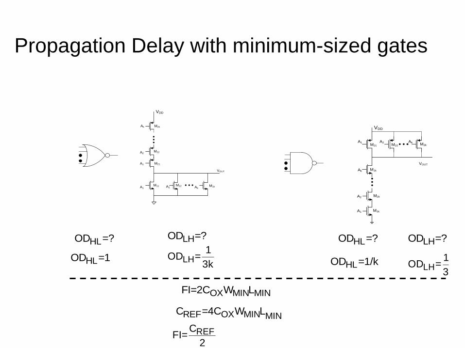
Propagation Delay with minimum-sized gates
VOUT
VDD
A1 A2 Ak
A1
A2
Ak
M11 M12 M1k
M21
M22
M2k
VOUT
M1k
M21
VDD
A1 A2 AkM22 M2k
A1
A2
Ak
M2k
M1k
HLOD =1 LH1
OD =3k HLOD =1/k
LH1
OD =3
HLOD =? HLOD =?LHOD =?LHOD =?
OX MIN MINFI=2C W L
REF OX MIN MINC =4C W L
REFCFI=
2
Propagation Delay in Multiple-Levels of
Logic with Stage LoadingMinimum-sized gates
CIN/CREF
Equal Rise/Fall
Inverter
NAND
NOR
1
3k+1
4
3+k
4
Minimum Sized
Overdrive
HL
LH
1
1
1/2
1/2
1/2
1
1/3NOR
NAND
Inverter
HL
LH
HL
LH
1
1
1
1
1
1/(3k)
1/k
1/3
Equal Rise/Fall(with OD)
OD
3k+1OD
4
3+kOD
4
OD
OD
OD
OD
OD
OD
n
I(k+1)
k=1 k
F
OD
n
I(k+1)
k=1
FtPROP/tREF1
n
I(k+1)
k=1 HLk LHk
1 1F
2 OD OD
VOUT
VDD
A1 A2 Ak
A1
A2
Ak
M11 M12 M1k
M21
M22
M2k
VOUT
M1k
M21
VDD
A1 A2 AkM22 M2k
A1
A2
Ak
M2k
M1k
HLOD =1LH
1OD =
3k
HLOD =1/k LH1
OD =3
REFCFI=
2
A
F
M
M
M
M
M M
M
M
M
M
M
M
M
M
M
20fF
50fF
Minimum-sized gates
HLOD =1
HLOD =1
HLOD =1
LHOD =1/3
LHOD =1/3
HL1
OD = =k
1/3
HL1
OD = =k
1/2
LH1
OD = =3k
1/12
LH1
OD = =3k
1/6
LH1
OD = =3k
1/9
20fF=5
4fFREF
C
C
50fF=12.5
4fFREF
C
C
1/2
1/2
1/2
1/2
1/2 1/2
1/21/2
1
5
PROP REF I(k+1)
k=1 HLk LHk
1 1t =t F
2 OD OD
FI2=13/2
FI3=1
FI4=1
FI5=1/2
FI6=12.5
13 1
3 3 1 12 1 1 6 10 9 1 12.5 2 32 2
PROP REF
1t =t
2
PROP REFt =63.25 t
ODHL
ODLH
Propagation Delay in Multiple-Levels of
Logic with Stage Loading
A
F4
2
4
2
4
2
1
1
1
1
1
1
1/2
1/4
1
1
4
1/4
1
2
2
1
1
2
1
2
1
2
20fF
50fF1
2
?PROP REFt = t
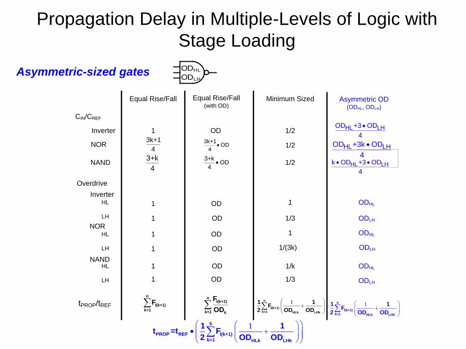
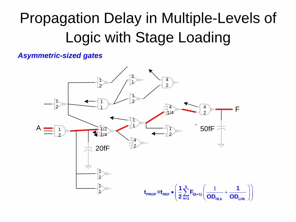
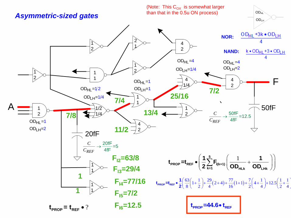
Asymmetric-sized gates
Propagation Delay in Multiple-Levels of Logic with
Stage Loading
Asymmetric-sized gates
CIN/CREF
Equal Rise/Fall
Inverter
NAND
NOR
1
3k+1
4
3+k
4
Minimum Sized
Overdrive
HL
LH
1
1
1/2
1/2
1/2
1
1/3NOR
NAND
Inverter
HL
LH
HL
LH
1
1
1
1
1
1/(3k)
1/k
1/3
Equal Rise/Fall(with OD)
OD
3k+1OD
4
3+kOD
4
Asymmetric OD (ODHL, ODLH)
HL LHOD +3 OD
4
OD
OD
OD
OD
OD
OD
HL LHOD +3k OD
4
HL LHk OD +3 OD
4
ODHL
ODLH
ODHL
ODLH
ODHL
ODLH
n
I(k+1)
k=1 k
F
OD
n
I(k+1)
k=1
F 1
n
I(k+1)
k=1 HLk LHk
1 1F
2 OD OD
tPROP/tREF1
n
I(k+1)
k=1 HLk LHk
1 1F
2 OD OD
ODHL
ODLH
1
5
PROP REF I(k+1)
k=1 HLk LHk
1 1t =t F
2 OD OD
Propagation Delay in Multiple-Levels of
Logic with Stage Loading
A
F4
2
4
2
4
2
1
1
1
1
1
1
1/2
1/4
1
1
4
1/4
1
2
2
1
1
2
1
2
1
2
20fF
50fF1
2
Asymmetric-sized gates
1
5
PROP REF I(k+1)
k=1 HLk LHk
1 1t =t F
2 OD OD
A
F4
2
4
2
4
2
1
1
1
1
1
1
1/2
1/4
1
1
4
1/4
1
2
2
1
1
2
1
2
1
2
20fF
50fF1
2
?PROP REFt = t
Asymmetric-sized gates
LHOD =2
HLOD =17/8
1
1
20fF=5
4fFREF
C
C
HLOD =1 2
LHOD =1/4
FI2=63/8
7/4
11/2
FI3=29/4
HLOD =1
LHOD =1
FI4=77/16
HLOD =4
LHOD =1/4
25/16
LHOD =2HLOD =4
50fF=12.5
4fFREF
C
C
FI5=7/2
FI6=12.5
1
5
PROP REF I(k+1)
k=1 HLk LHk
1 1t =t F
2 OD OD
63 1 29 77 7 1 1 1
1 2 4 1 1 4 12.58 2 4 16 2 4 2 4
PROP REF
1t =t
2
PROP REFt =44.6 t
ODHL
ODLH
NOR:
NAND:
7/2
13/4
(Note: This COX is somewhat larger
than that in the 0.5u ON process)
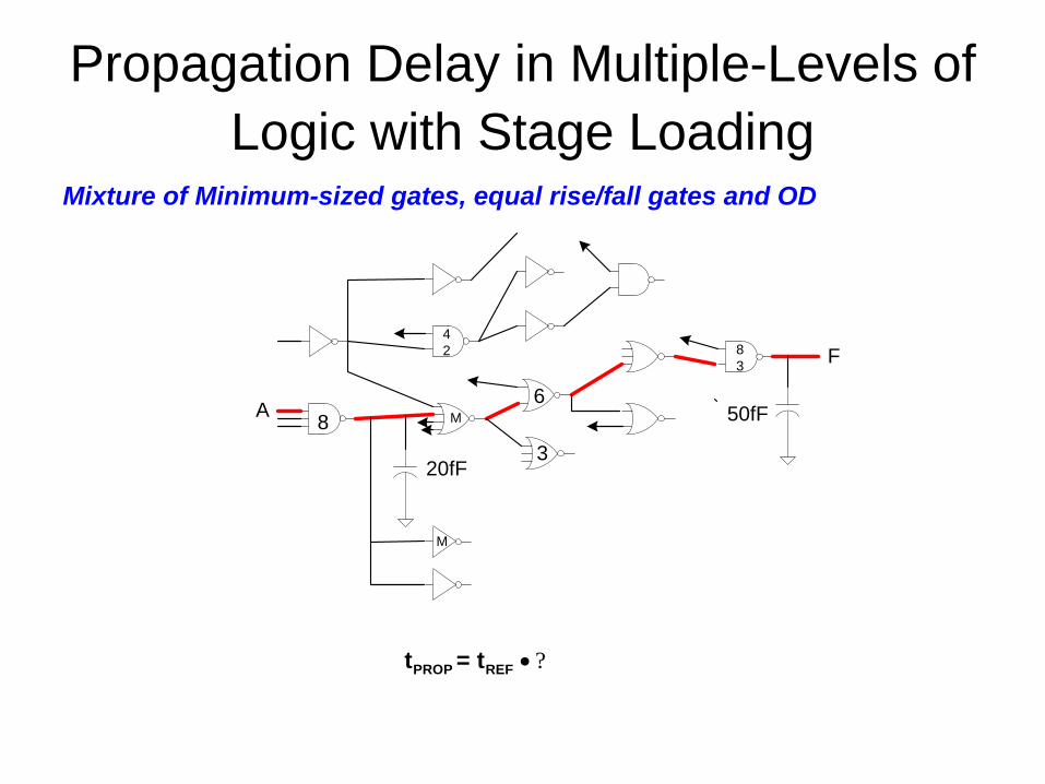
Propagation Delay in Multiple-Levels of
Logic with Stage Loading
A
F
8
6M
M
320fF
50fF
8
3
4
2
Mixture of Minimum-sized gates, equal rise/fall gates and OD
?PROP REFt = t
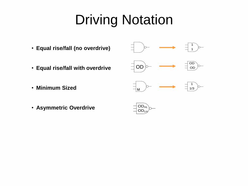
Driving Notation
• Equal rise/fall (no overdrive)
• Equal rise/fall with overdrive
• Minimum Sized
• Asymmetric Overdrive
OD
ODHL
ODLH
M
1
1
OD
OD
1
1/3
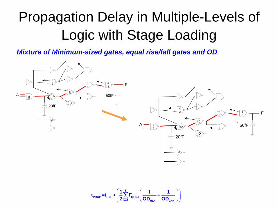
Propagation Delay in Multiple-Levels of
Logic with Stage Loading
A
F
8
6M
M
320fF
50fF
8
3
4
2
Mixture of Minimum-sized gates, equal rise/fall gates and OD
1
5
PROP REF I(k+1)
k=1 HLk LHk
1 1t =t F
2 OD OD
A
F
8
6
M
320fF
50fF
8
3
4
2
811/3
6
11
Propagation Delay in Multiple-Levels of
Logic with Stage LoadingMixture of Minimum-sized gates, equal rise/fall gates and OD
1
5
PROP REF I(k+1)
k=1 HLk LHk
1 1t =t F
2 OD OD
A
F
8
6
M
3
20fF
50fF
8
3
4
2
811/3
6
11
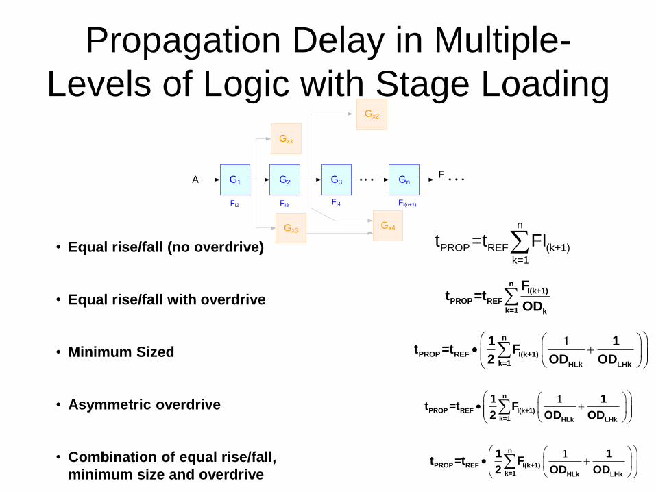
Propagation Delay in Multiple-
Levels of Logic with Stage Loading
nI(k+1)
PROP REF
k=1 k
Ft =t
OD
• Equal rise/fall (no overdrive)
• Equal rise/fall with overdrive
• Minimum Sized
• Asymmetric overdrive
• Combination of equal rise/fall,
minimum size and overdrive
n
PROP REF (k+1)
k=1
t =t FI
G1 G2 G3 GnAF
FI2 FI3 FI4 FI(n+1)
Gxx
Gx2
Gx3Gx4
1
n
PROP REF I(k+1)
k=1 HLk LHk
1 1t =t F
2 OD OD
1
n
PROP REF I(k+1)
k=1 HLk LHk
1 1t =t F
2 OD OD
1
n
PROP REF I(k+1)
k=1 HLk LHk
1 1t =t F
2 OD OD
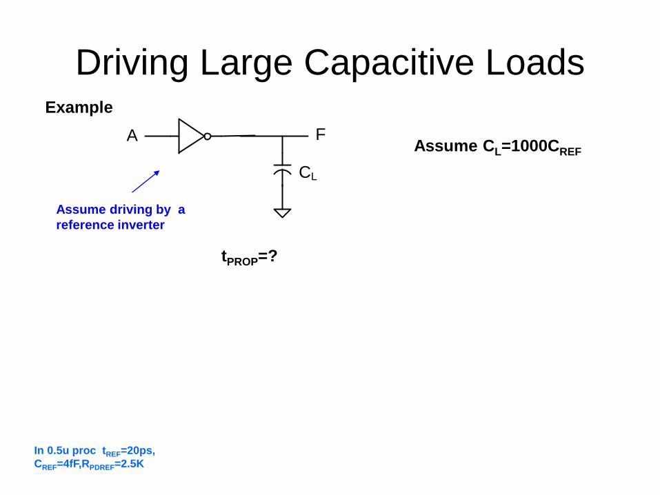
Driving Large Capacitive Loads
A F
CL
Assume driving by a
reference inverter
Assume CL=1000CREF
In 0.5u proc tREF=20ps,
CREF=4fF,RPDREF=2.5K
Example
tPROP=?
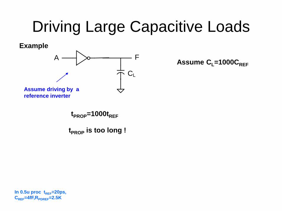
Driving Large Capacitive Loads
A F
CL
Assume driving by a
reference inverter
Assume CL=1000CREF
In 0.5u proc tREF=20ps,
CREF=4fF,RPDREF=2.5K
Example
tPROP=1000tREF
tPROP is too long !
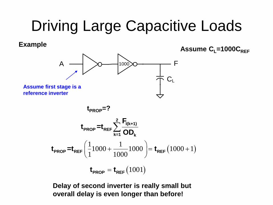
Driving Large Capacitive Loads
A F
CL
1000
Assume first stage is a
reference inverter
ExampleAssume CL=1000CREF
tPROP=?
2
I(k+1)
PROP REF
k=1 k
Ft =t
OD
1 1
1000 1000 1000 11 1000
PROP REF REFt =t t
1001PROP REFt t
Delay of second inverter is really small but
overall delay is even longer than before!
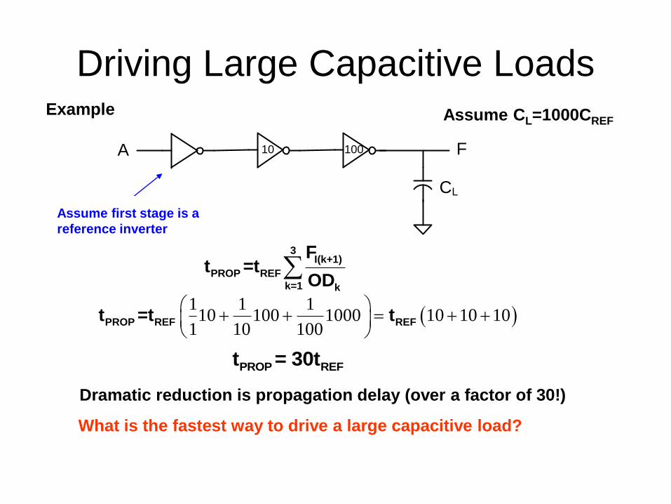
Driving Large Capacitive Loads
A F
CL
10 100
Assume first stage is a
reference inverter
Example Assume CL=1000CREF
3
I(k+1)
PROP REF
k=1 k
Ft =t
OD
1 1 1
10 100 1000 10 10 101 10 100
PROP REF REFt =t t
PROP REFt = 30t
Dramatic reduction is propagation delay (over a factor of 30!)
What is the fastest way to drive a large capacitive load?
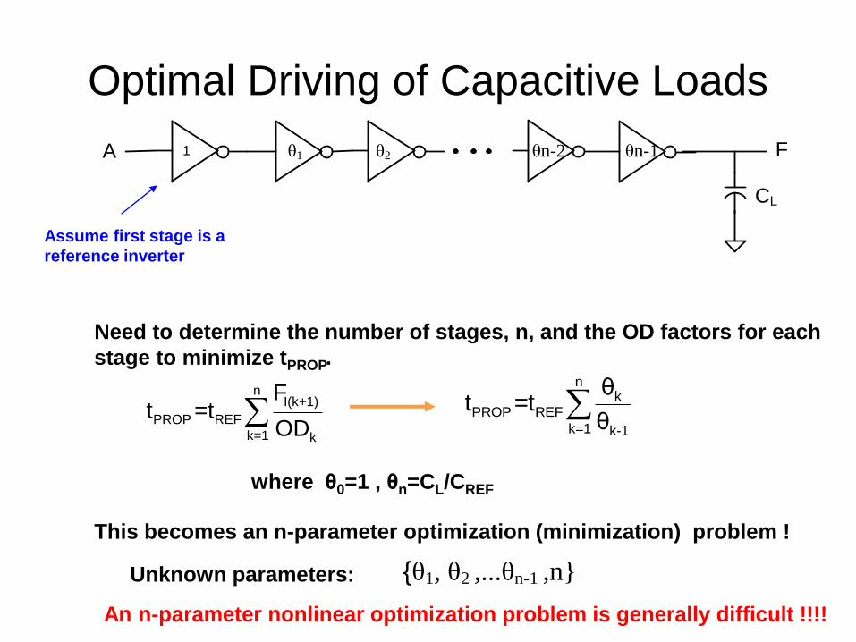
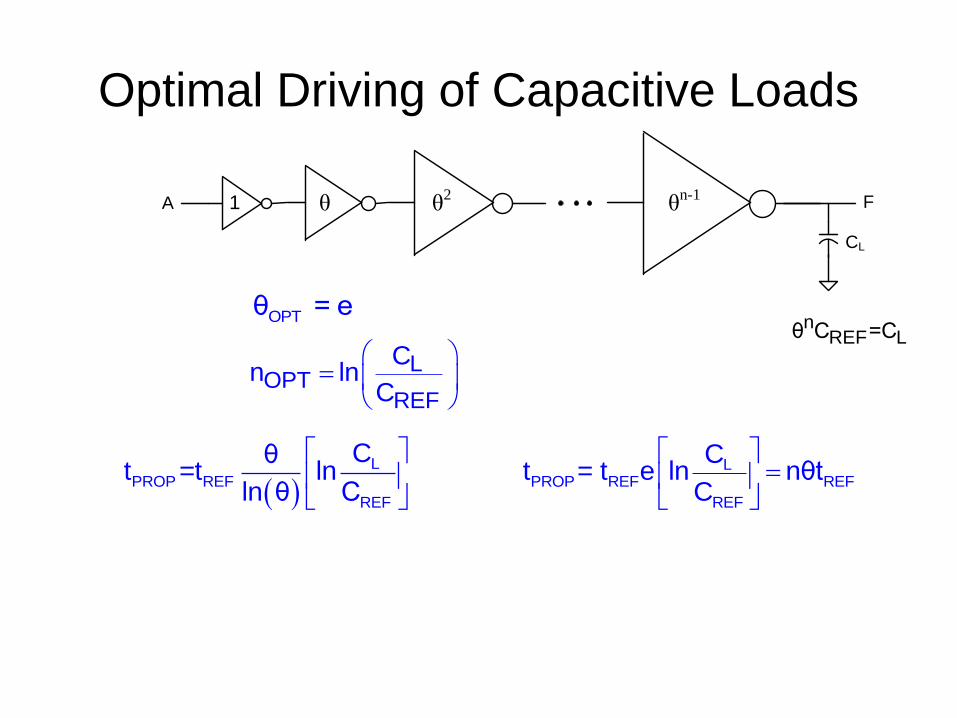
Optimal Driving of Capacitive Loads
Assume first stage is a
reference inverter
A F
CL
1 θ1 θn-1θn-2θ2
Need to determine the number of stages, n, and the OD factors for each
stage to minimize tPROP.
{θ1, θ2 ,...θn-1 ,n}
nk
PROP REF
k=1 k-1
θt =t
θ
nI(k+1)
PROP REF
k=1 k
Ft =t
OD
where θ0=1 , θn=CL/CREF
This becomes an n-parameter optimization (minimization) problem !
Unknown parameters:
An n-parameter nonlinear optimization problem is generally difficult !!!!
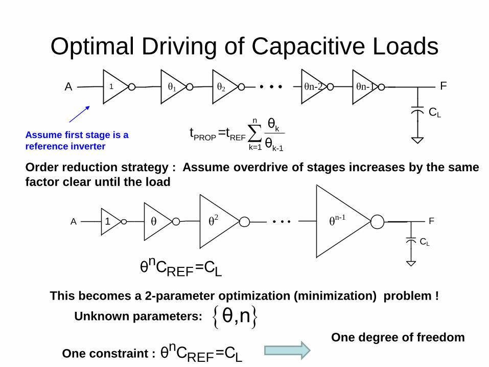
Optimal Driving of Capacitive Loads
Assume first stage is a
reference inverter
A F
CL
1 θ1 θn-1θn-2θ2
nk
PROP REF
k=1 k-1
θt =t
θ
This becomes a 2-parameter optimization (minimization) problem !
Unknown parameters:
Order reduction strategy : Assume overdrive of stages increases by the same
factor clear until the load
A F
CL
1 θ θ2 θn-1
nREF Lθ C =C
θ,n
One constraint :n
REF Lθ C =COne degree of freedom
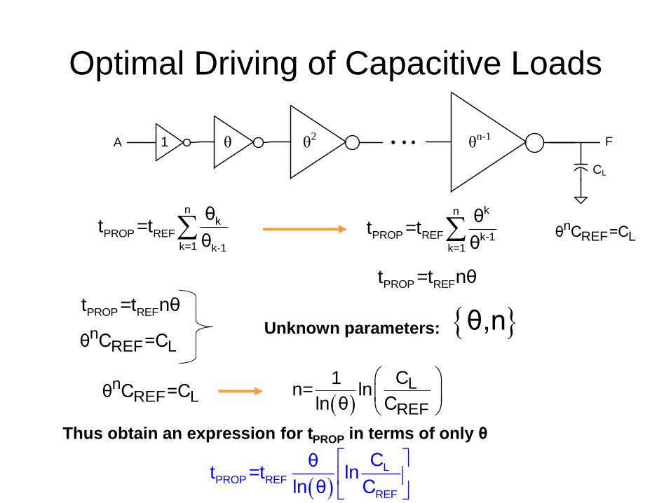
Optimal Driving of Capacitive Loads
kn
PROP REF k-1k=1
θt =t
θ
Unknown parameters:
A F
CL
1 θ θ2 θn-1
θ,n
nk
PROP REF
k=1 k-1
θt =t
θ n
REF Lθ C =C
PROP REFt =t nθ
PROP REFt =t nθ
nREF Lθ C =C
nREF Lθ C =C
L
REF
C1n= ln
ln θ C
L
PROP REF
REF
Cθt =t ln
ln θ C
Thus obtain an expression for tPROP in terms of only θ
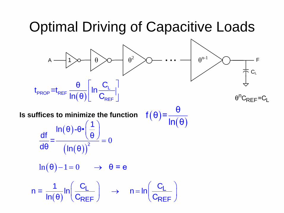
Optimal Driving of Capacitive Loads
A F
CL
1 θ θ2 θn-1
nREF Lθ C =C
LPROP REF
REF
Cθt =t ln
ln θ C
Is suffices to minimize the function θ
f θ =ln θ
0
2
1ln θ -θ•
df θ=
dθ ln θ
ln 1 0θ θ = e
L L
REF REF
C C1n = ln n ln
ln θ C C
Optimal Driving of Capacitive Loads
A F
CL
1 θ θ2 θn-1
nREF Lθ C =C
L
PROP REF
REF
Cθt =t ln
ln θ C
OPTθ = e
LOPT
REF
Cn ln
C
LPROP REF REF
REF
Ct = t e ln nθt
C
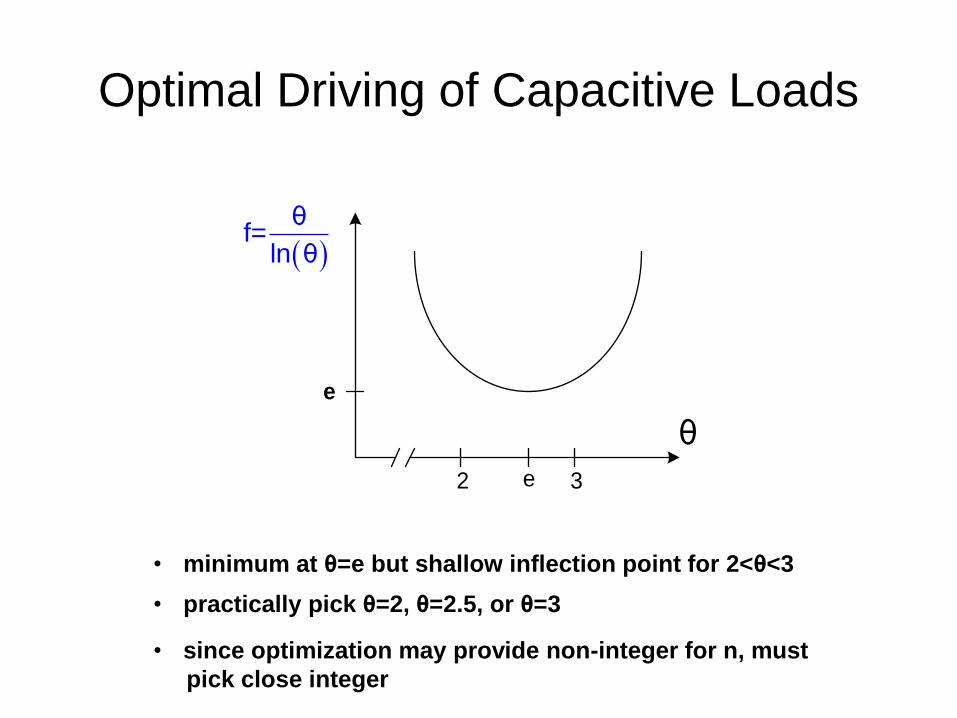
Optimal Driving of Capacitive Loads
θ
2 3e
e
• minimum at θ=e but shallow inflection point for 2<θ<3
θ
f=ln θ
• practically pick θ=2, θ=2.5, or θ=3
• since optimization may provide non-integer for n, must
pick close integer
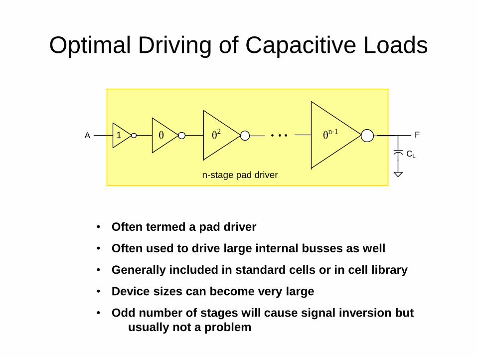
Optimal Driving of Capacitive Loads
A F
CL
1 θ θ2 θn-1
n-stage pad driver
• Often termed a pad driver
• Often used to drive large internal busses as well
• Generally included in standard cells or in cell library
• Device sizes can become very large
• Odd number of stages will cause signal inversion but
usually not a problem
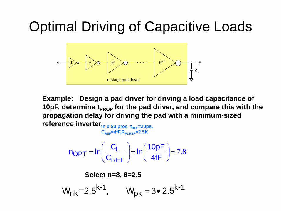
Optimal Driving of Capacitive Loads
A F
CL
1 θ θ2 θn-1
n-stage pad driver
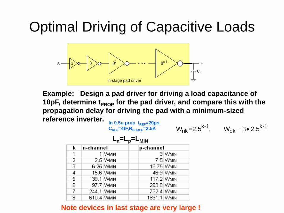
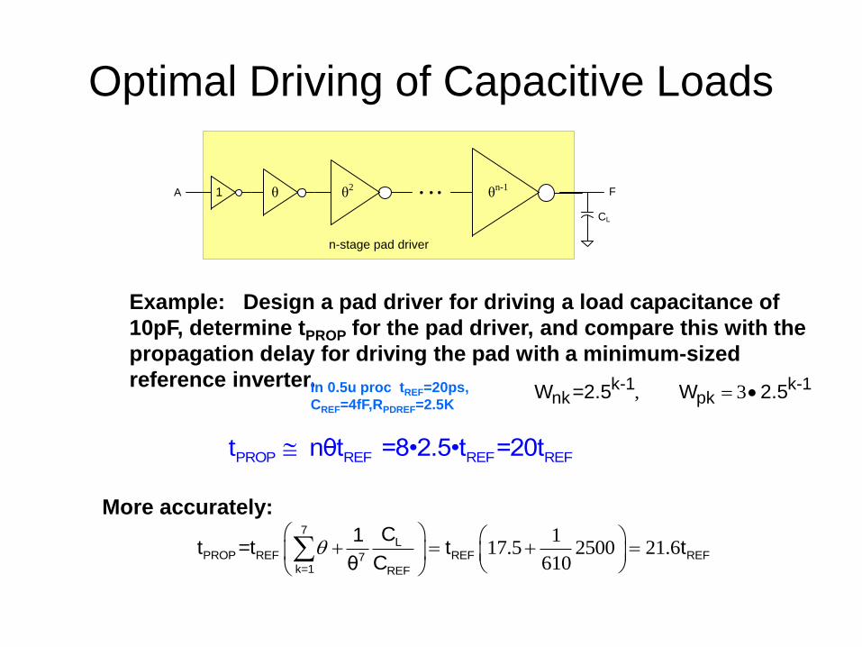
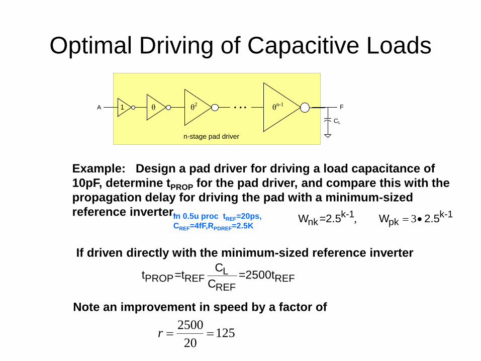
Example: Design a pad driver for driving a load capacitance of
10pF, determine tPROP for the pad driver, and compare this with the
propagation delay for driving the pad with a minimum-sized
reference inverter.In 0.5u proc tREF=20ps,
CREF=4fF,RPDREF=2.5K
7.8LOPT
REF
C 10pFn ln ln
C 4fF
Select n=8, θ=2.5
, 3k-1 k-1nk pkW =2.5 W 2.5
Optimal Driving of Capacitive Loads
A F
CL
1 θ θ2 θn-1
n-stage pad driver
Example: Design a pad driver for driving a load capacitance of
10pF, determine tPROP for the pad driver, and compare this with the
propagation delay for driving the pad with a minimum-sized
reference inverter.In 0.5u proc tREF=20ps,
CREF=4fF,RPDREF=2.5K , 3k-1 k-1nk pkW =2.5 W 2.5
Ln=Lp=LMIN
Note devices in last stage are very large !
Optimal Driving of Capacitive Loads
A F
CL
1 θ θ2 θn-1
n-stage pad driver
Example: Design a pad driver for driving a load capacitance of
10pF, determine tPROP for the pad driver, and compare this with the
propagation delay for driving the pad with a minimum-sized
reference inverter.In 0.5u proc tREF=20ps,
CREF=4fF,RPDREF=2.5K, 3k-1 k-1
nk pkW =2.5 W 2.5
PROP REF REF REFt nθt =8•2.5•t =20t
117.5 2500 21.6
610
7L
PROP REF REF REF7k=1 REF
C1t =t t t
Cθ
More accurately:
Optimal Driving of Capacitive Loads
A F
CL
1 θ θ2 θn-1
n-stage pad driver
Example: Design a pad driver for driving a load capacitance of
10pF, determine tPROP for the pad driver, and compare this with the
propagation delay for driving the pad with a minimum-sized
reference inverter.In 0.5u proc tREF=20ps,
CREF=4fF,RPDREF=2.5K, 3k-1 k-1
nk pkW =2.5 W 2.5
If driven directly with the minimum-sized reference inverter
LPROP REF REF
REF
Ct =t =2500t
C
Note an improvement in speed by a factor of
2500125
20r

Optimal Driving of Capacitive Loads
A F
CL
1 θ θ2 θn-1
n-stage pad driver
Example: Design a pad driver for driving a load capacitance of
10pF, determine tPROP for the pad driver, and compare this with the
propagation delay for driving the pad with a minimum-sized
reference inverter.In 0.5u proc tREF=20ps,
CREF=4fF,RPDREF=2.5K , 3k-1 k-1nk pkW =2.5 W 2.5
Ln=Lp=LMIN
Note devices in last stage are very large !
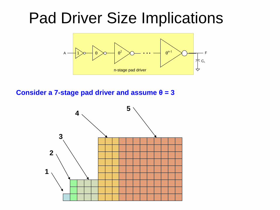
Pad Driver Size Implications
A F
CL
1 θ θ2 θn-1
n-stage pad driver
1
2
3
45
Consider a 7-stage pad driver and assume θ = 3
6 7
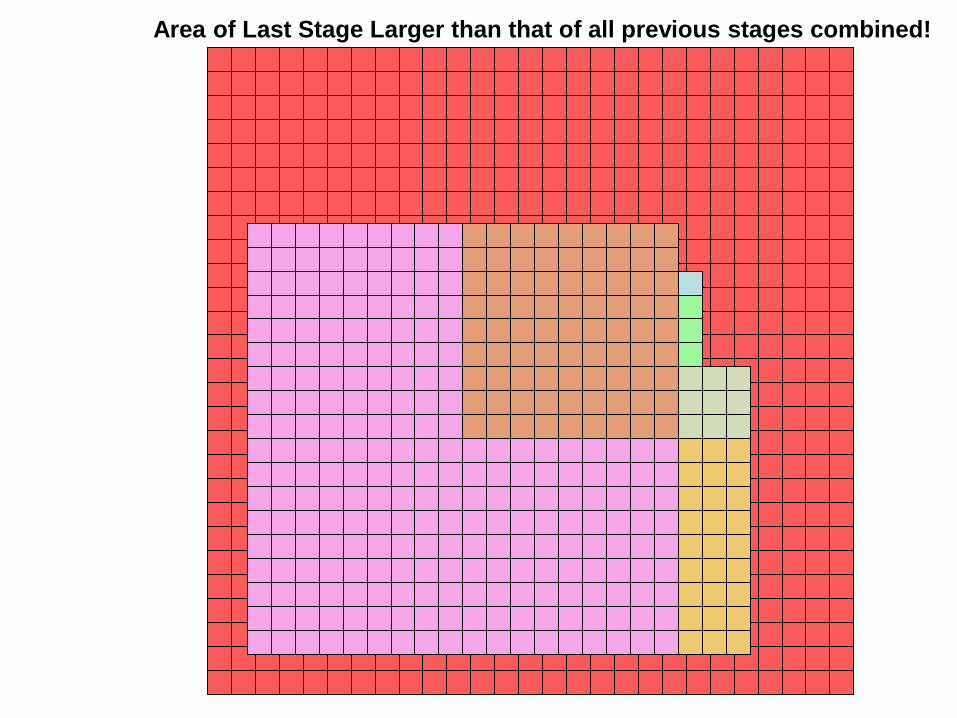
Area of Last Stage Larger than that of all previous stages combined!

End of Lecture 41

![t Z v v Á } l vbhiksha/courses/deeplearning/Spring.2018/... · 2018. 1. 22. · d l Z u } ] o Ç EE U l o v ] v P î Z W EE v Z ] v](https://img.pdfslide.net/doc/110x75/60c5177c8d3ae846c1659058/t-z-v-v-l-v-bhikshacoursesdeeplearningspring2018-2018-1-22-d.jpg)


![DRAGON'S LAIR G e n e v i e v e D i d i o n K - 8 M a y 2 ... · upcoming events ee]a ee]a a ee]a a ee]a ee]a a a ee]a ee]a ee]a ee]a ee]a ee]a ee]a ee]a ee]a dragon's lair g e n](https://img.pdfslide.net/doc/110x75/5edb079c09ac2c67fa68b1f0/dragons-lair-g-e-n-e-v-i-e-v-e-d-i-d-i-o-n-k-8-m-a-y-2-upcoming-events-eea.jpg)