Embed Size (px)
Citation preview
Page 1 of 15
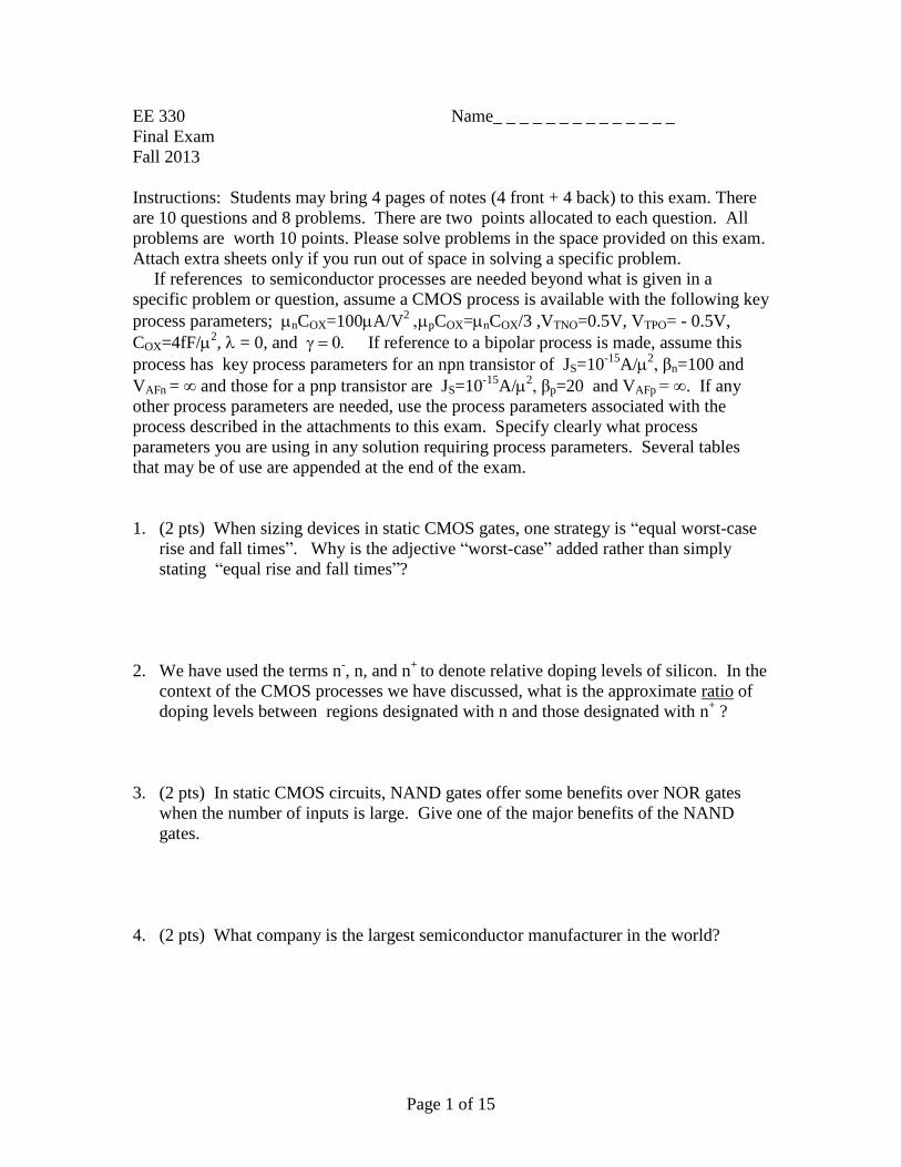
EE 330 Name_ _ _ _ _ _ _ _ _ _ _ _ _ _
Final Exam
Fall 2013
Instructions: Students may bring 4 pages of notes (4 front + 4 back) to this exam. There
are 10 questions and 8 problems. There are two points allocated to each question. All
problems are worth 10 points. Please solve problems in the space provided on this exam.
Attach extra sheets only if you run out of space in solving a specific problem.
If references to semiconductor processes are needed beyond what is given in a
specific problem or question, assume a CMOS process is available with the following key
process parameters; nCOX=100A/V2 pCOX=nCOX/3 ,VTNO=0.5V, VTPO= - 0.5V,
COX=4fF/2, = 0, and If reference to a bipolar process is made, assume this
process has key process parameters for an npn transistor of JS=10-15
A/2, βn=100 and
VAFn = ∞ and those for a pnp transistor are JS=10-15
A/2, βp=20 and VAFp = ∞. If any
other process parameters are needed, use the process parameters associated with the
process described in the attachments to this exam. Specify clearly what process
parameters you are using in any solution requiring process parameters. Several tables
that may be of use are appended at the end of the exam.
1. (2 pts) When sizing devices in static CMOS gates, one strategy is “equal worst-case
rise and fall times”. Why is the adjective “worst-case” added rather than simply
stating “equal rise and fall times”?
2. We have used the terms n-, n, and n
+ to denote relative doping levels of silicon. In the
context of the CMOS processes we have discussed, what is the approximate ratio of
doping levels between regions designated with n and those designated with n+ ?
3. (2 pts) In static CMOS circuits, NAND gates offer some benefits over NOR gates
when the number of inputs is large. Give one of the major benefits of the NAND
gates.
4. (2 pts) What company is the largest semiconductor manufacturer in the world?
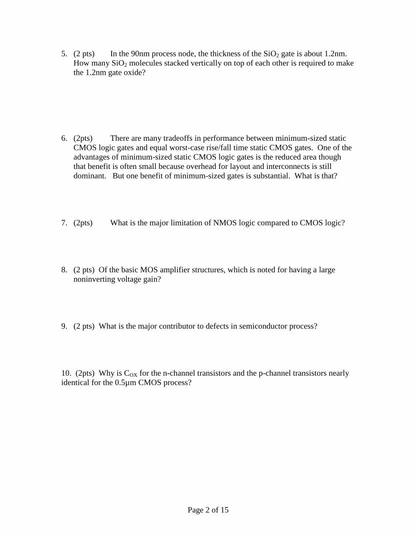
Page 2 of 15
5. (2 pts) In the 90nm process node, the thickness of the SiO2 gate is about 1.2nm.
How many SiO2 molecules stacked vertically on top of each other is required to make
the 1.2nm gate oxide?
6. (2pts) There are many tradeoffs in performance between minimum-sized static
CMOS logic gates and equal worst-case rise/fall time static CMOS gates. One of the
advantages of minimum-sized static CMOS logic gates is the reduced area though
that benefit is often small because overhead for layout and interconnects is still
dominant. But one benefit of minimum-sized gates is substantial. What is that?
7. (2pts) What is the major limitation of NMOS logic compared to CMOS logic?
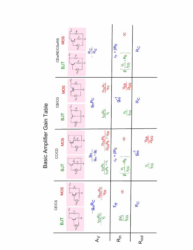
8. (2 pts) Of the basic MOS amplifier structures, which is noted for having a large
noninverting voltage gain?
9. (2 pts) What is the major contributor to defects in semiconductor process?
10. (2pts) Why is COX for the n-channel transistors and the p-channel transistors nearly
identical for the 0.5µm CMOS process?
Page 3 of 15
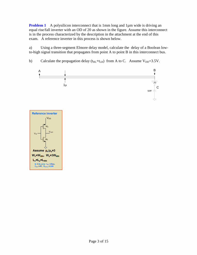
Problem 1 A polysilicon interconnect that is 1mm long and 1µm wide is driving an
equal rise/fall inverter with an OD of 20 as shown in the figure. Assume this interconnect
is in the process characterized by the description in the attachment at the end of this
exam. A reference inverter in this process is shown below.
a) Using a three-segment Elmore delay model, calculate the delay of a Boolean low-
to-high signal transition that propagates from point A to point B in this interconnect bus.
b) Calculate the propagation delay (tHL+tLH) from A to C. Assume VDD=3.5V.
1μ
50fF
A B
20
C
Page 4 of 15
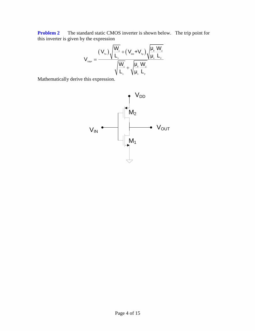
Problem 2 The standard static CMOS inverter is shown below. The trip point for
this inverter is given by the expression
Mathematically derive this expression.
M1
M2
VDD
VINVOUT
p1 2
Tn DD Tp
1 n 2
TRIP
p1 2
1 n 2
μW WV V +V
L μ LV
μW W
L μ L
Page 5 of 15
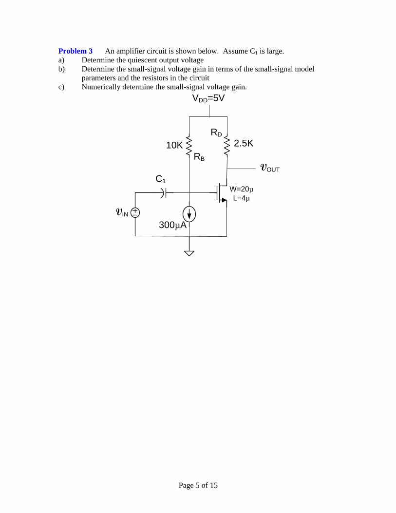
Problem 3 An amplifier circuit is shown below. Assume C1 is large.
a) Determine the quiescent output voltage
b) Determine the small-signal voltage gain in terms of the small-signal model
parameters and the resistors in the circuit
c) Numerically determine the small-signal voltage gain.
VIN
VOUT
VDD=5V
C1
W=20µ
L=4µ
10K
300µA
2.5K
RB
RD
Page 6 of 15
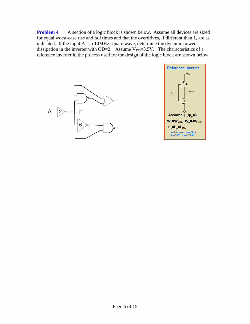
Problem 4 A section of a logic block is shown below. Assume all devices are sized
for equal worst-case rise and fall times and that the overdrives, if different than 1, are as
indicated. If the input A is a 10MHz square wave, determine the dynamic power
dissipation in the inverter with OD=2. Assume VDD=3.5V. The characteristics of a
reference inverter in the process used for the design of the logic block are shown below.
A F
6
2
Page 7 of 15
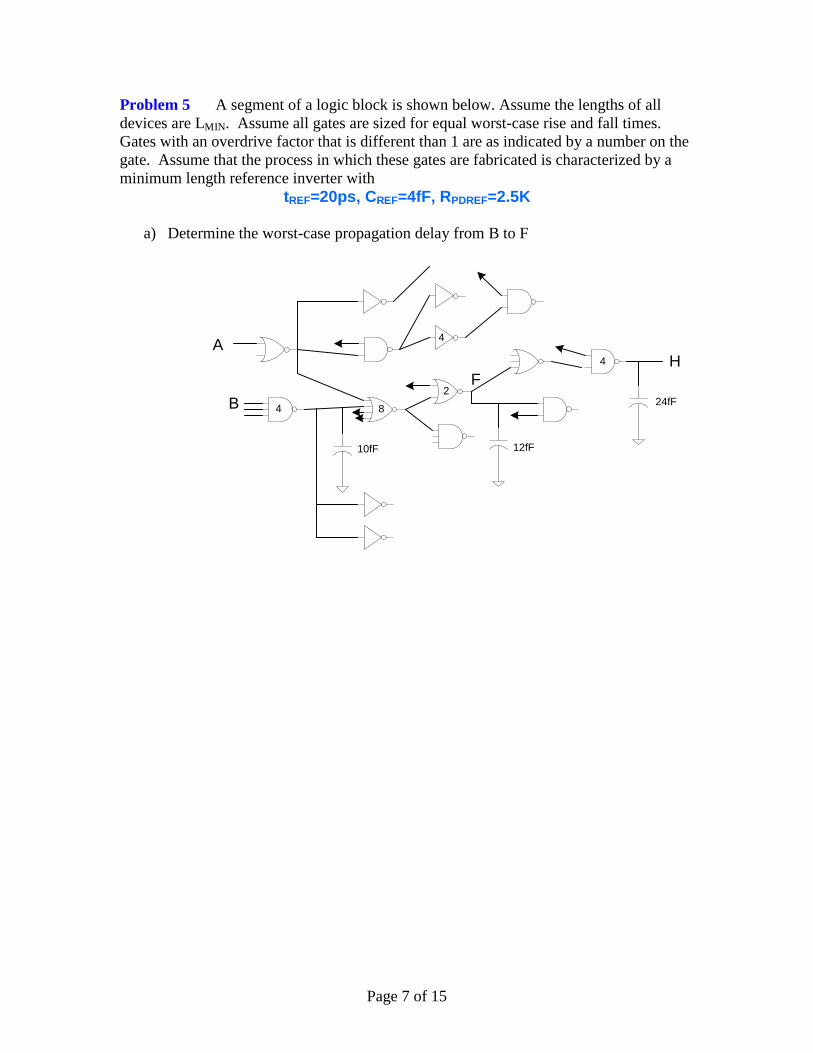
Problem 5 A segment of a logic block is shown below. Assume the lengths of all
devices are LMIN. Assume all gates are sized for equal worst-case rise and fall times.
Gates with an overdrive factor that is different than 1 are as indicated by a number on the
gate. Assume that the process in which these gates are fabricated is characterized by a
minimum length reference inverter with
tREF=20ps, CREF=4fF, RPDREF=2.5K
a) Determine the worst-case propagation delay from B to F
4
4
8
A
B
F
4
2
10fF 12fF
24fF
H
Page 8 of 15
b) Repeat part a) if all gates are minimum sized.
Page 9 of 15
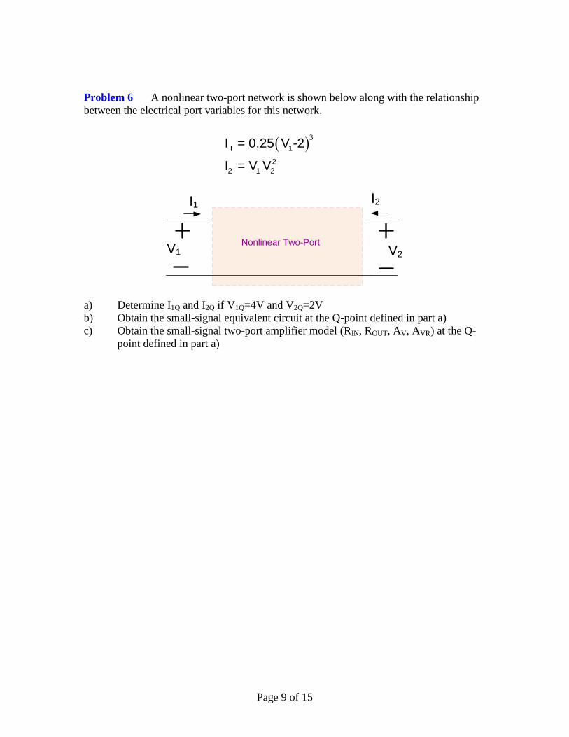
Problem 6 A nonlinear two-port network is shown below along with the relationship
between the electrical port variables for this network.
V2V1
I1 I2
Nonlinear Two-Port
3
I 1
2
2 1 2
I = 0.25 V -2
I = V V
a) Determine I1Q and I2Q if V1Q=4V and V2Q=2V
b) Obtain the small-signal equivalent circuit at the Q-point defined in part a)
c) Obtain the small-signal two-port amplifier model (RIN, ROUT, AV, AVR) at the Q-
point defined in part a)
Page 10 of 15
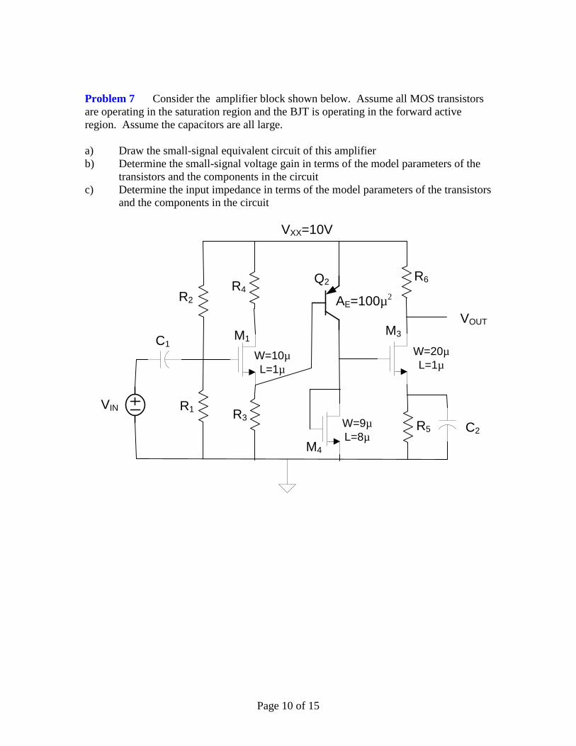
Problem 7 Consider the amplifier block shown below. Assume all MOS transistors
are operating in the saturation region and the BJT is operating in the forward active
region. Assume the capacitors are all large.
a) Draw the small-signal equivalent circuit of this amplifier
b) Determine the small-signal voltage gain in terms of the model parameters of the
transistors and the components in the circuit
c) Determine the input impedance in terms of the model parameters of the transistors
and the components in the circuit
Q2
M4
M3M1
R1R3
R2
R5
R4
VOUT
VIN
VXX=10V
W=10µ
L=1µ
W=20µ
L=1µ
W=9µ
L=8µ
AE=100µ2
R6
C1
C2
Page 11 of 15
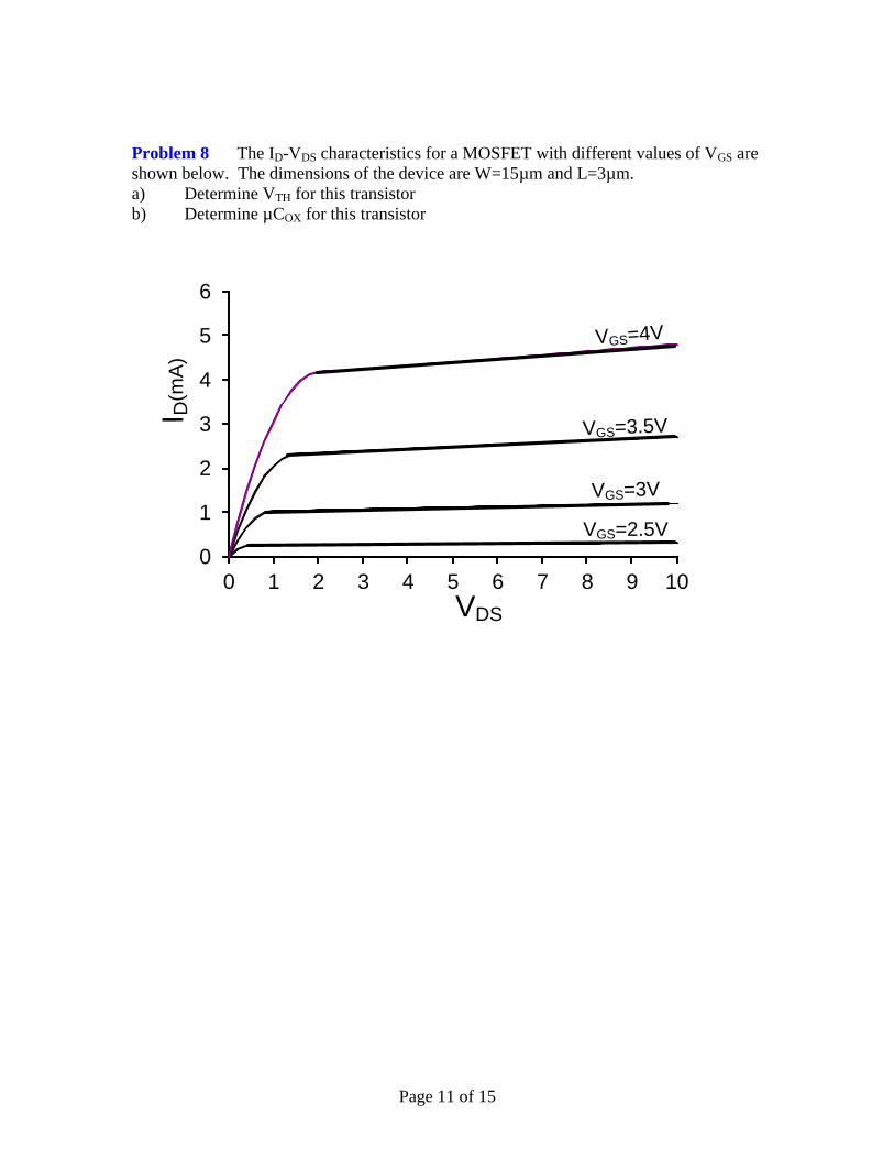
Problem 8 The ID-VDS characteristics for a MOSFET with different values of VGS are
shown below. The dimensions of the device are W=15µm and L=3µm.
a) Determine VTH for this transistor
b) Determine µCOX for this transistor
0
1
2
3
4
5
6
0 1 2 3 4 5 6 7 8 9 10
ID(m
A)
VDS
VGS=2.5V
VGS=3V
VGS=3.5V
VGS=4V
VDS
I D(m
A)
Page 12 of 15
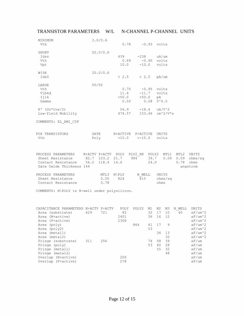
TRANSISTOR PARAMETERS W/L N-CHANNEL P-CHANNEL UNITS
MINIMUM 3.0/0.6
Vth 0.78 -0.93 volts
SHORT 20.0/0.6
Idss 439 -238 uA/um
Vth 0.69 -0.90 volts
Vpt 10.0 -10.0 volts
WIDE 20.0/0.6
Ids0 < 2.5 < 2.5 pA/um
LARGE 50/50
Vth 0.70 -0.95 volts
Vjbkd 11.4 -11.7 volts
Ijlk <50.0 <50.0 pA
Gamma 0.50 0.58 V^0.5
K' (Uo*Cox/2) 56.9 -18.4 uA/V^2
Low-field Mobility 474.57 153.46 cm^2/V*s
COMMENTS: XL_AMI_C5F
FOX TRANSISTORS GATE N+ACTIVE P+ACTIVE UNITS
Vth Poly >15.0 <-15.0 volts
PROCESS PARAMETERS N+ACTV P+ACTV POLY PLY2_HR POLY2 MTL1 MTL2 UNITS
Sheet Resistance 82.7 103.2 21.7 984 39.7 0.09 0.09 ohms/sq
Contact Resistance 56.2 118.4 14.6 24.0 0.78 ohms
Gate Oxide Thickness 144 angstrom
PROCESS PARAMETERS MTL3 N\PLY N_WELL UNITS
Sheet Resistance 0.05 824 815 ohms/sq
Contact Resistance 0.78 ohms
COMMENTS: N\POLY is N-well under polysilicon.
CAPACITANCE PARAMETERS N+ACTV P+ACTV POLY POLY2 M1 M2 M3 N_WELL UNITS
Area (substrate) 429 721 82 32 17 10 40 aF/um^2
Area (N+active) 2401 36 16 12 aF/um^2
Area (P+active) 2308 aF/um^2
Area (poly) 864 61 17 9 aF/um^2
Area (poly2) 53 aF/um^2
Area (metal1) 34 13 aF/um^2
Area (metal2) 32 aF/um^2
Fringe (substrate) 311 256 74 58 39 aF/um
Fringe (poly) 53 40 28 aF/um
Fringe (metal1) 55 32 aF/um
Fringe (metal2) 48 aF/um
Overlap (N+active) 206 aF/um
Overlap (P+active) 278 aF/um
Page 13 of 15
Page 14 of 15
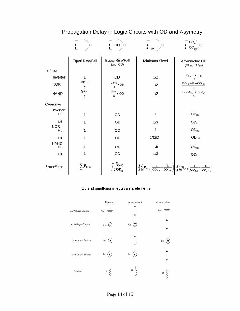
CIN/CREF
Equal Rise/Fall
Inverter
NAND
NOR
1
3k+1
4
3+k
4
Minimum Sized
Overdrive
HL
LH
1
1
1/2
1/2
1/2
1
1/3NOR
NAND
Inverter
HL
LH
HL
LH
1
1
1
1
1
1/(3k)
1/k
1/3
Equal Rise/Fall(with OD)
OD
3k+1OD
4
3+kOD
4
Asymmetric OD (ODHL, ODLH)
HL LHOD +3 OD
4
OD
OD
OD
OD
OD
OD
HL LHOD +3k OD
4
HL LHk OD +3 OD
4
ODHL
ODLH
ODHL
ODLH
ODHL
ODLH
n
I(k+1)
k=1 k
F
OD
n
I(k+1)
k=1
F 1
n
I(k+1)
k=1 HLk LHk
1 1F
2 OD ODtPROP/tREF
1
n
I(k+1)
k=1 HLk LHk
1 1F
2 OD OD
MOD
HL
LH
OD
OD
Propagation Delay in Logic Circuits with OD and Asymetry
Page 15 of 15


![EE 330 Lecture 42 - Iowa State Universityclass.ece.iastate.edu/ee330/lectures/EE 330 Lect 42 Fall 2016.pdf · EE 330 Lecture 42 Digital Circuits • Elmore Delay ... Elmore delay[1]](https://img.pdfslide.net/doc/110x75/5b57fe847f8b9a4e1b8b664d/ee-330-lecture-42-iowa-state-330-lect-42-fall-2016pdf-ee-330-lecture-42-digital.jpg)