Embed Size (px)
Citation preview
EE1411
MemorySTMicroIntelUCSDTHNU
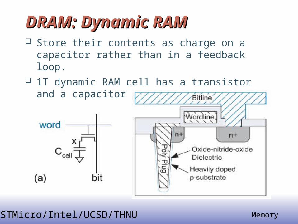
DRAM Dynamic RAMDRAM Dynamic RAM Store their contents as charge on a capacitor rather
than in a feedback loop 1T dynamic RAM cell has a transistor and a capacitor
EE1412
MemorySTMicroIntelUCSDTHNU
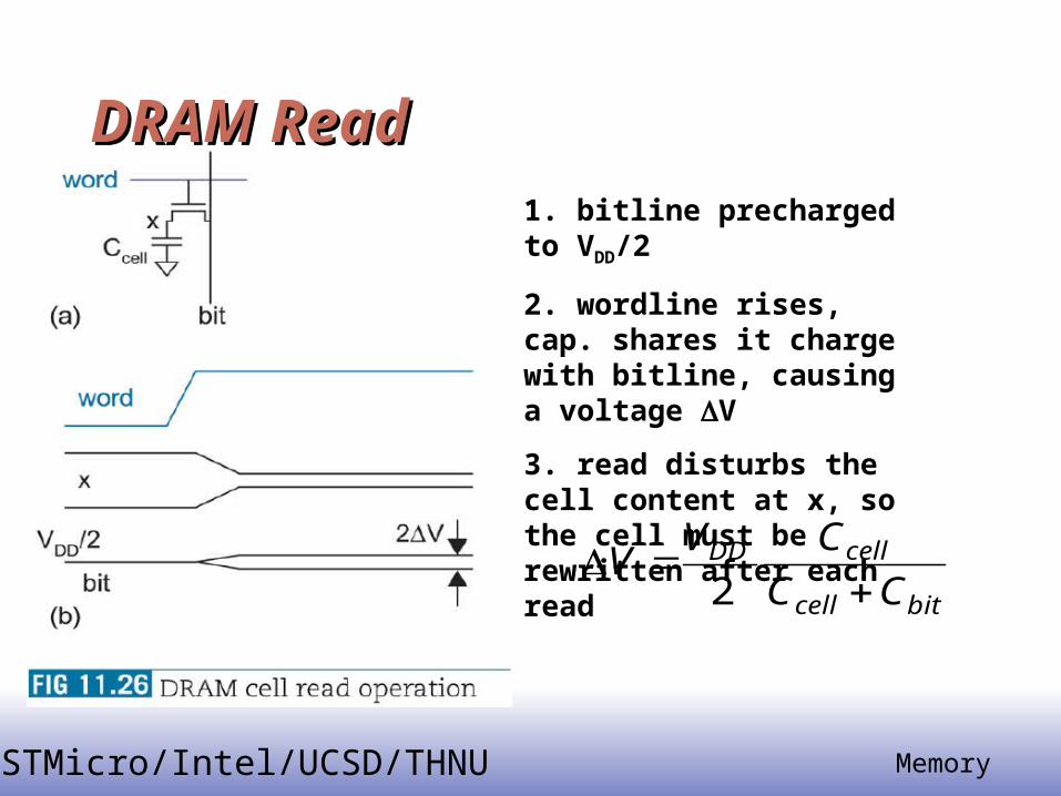
DRAM ReadDRAM Read1 bitline precharged to VDD2
2 wordline rises cap shares it charge with bitline causing a voltage V
3 read disturbs the cell content at x so the cell must be rewritten after each read
bitcell
cellDD
CC
CVV
2
EE1413
MemorySTMicroIntelUCSDTHNU
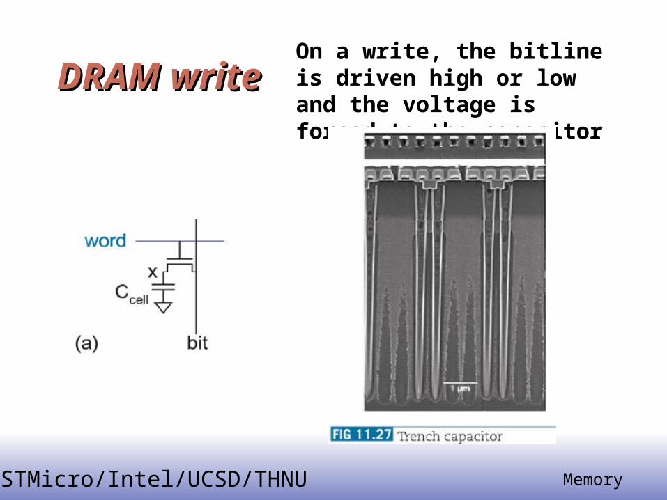
DRAM writeDRAM writeOn a write the bitline is driven high or low and the voltage is forced to the capacitor
EE1414
MemorySTMicroIntelUCSDTHNU
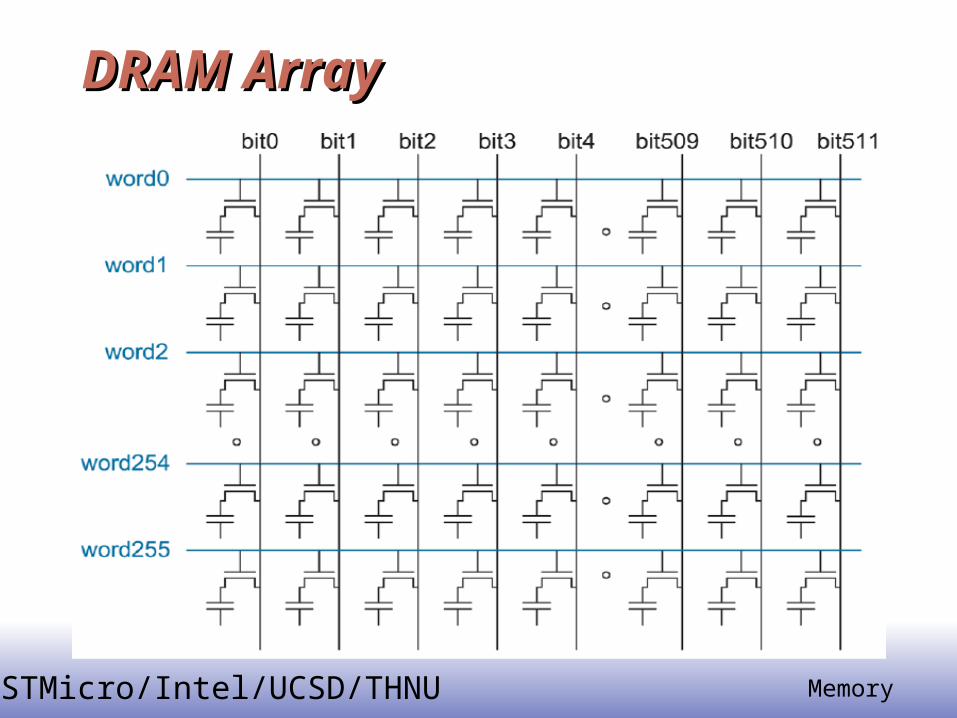
DRAM ArrayDRAM Array
EE1415
MemorySTMicroIntelUCSDTHNU
DRAMDRAM
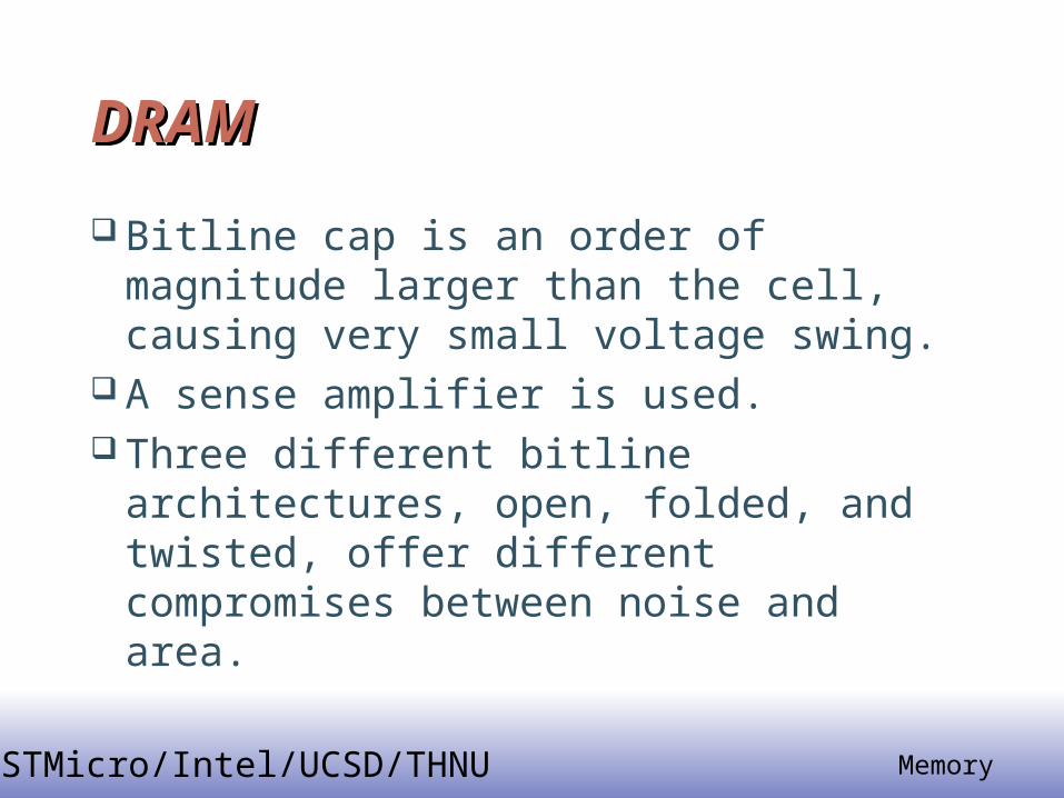
Bitline cap is an order of magnitude larger than the cell causing very small voltage swing
A sense amplifier is used Three different bitline architectures
open folded and twisted offer different compromises between noise and area
EE1416
MemorySTMicroIntelUCSDTHNU
DRAM in a nutshellDRAM in a nutshell
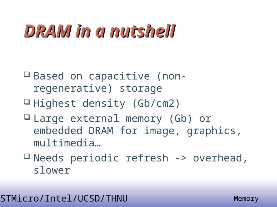
Based on capacitive (non-regenerative) storage
Highest density (Gbcm2) Large external memory (Gb) or embedded
DRAM for image graphics multimediahellip Needs periodic refresh -gt overhead slower
EE1417
MemorySTMicroIntelUCSDTHNU
EE1418
MemorySTMicroIntelUCSDTHNU
Classical DRAM Organization Classical DRAM Organization (square)(square)
row
decoder
rowaddress
Column Selector amp IO Circuits Column
Address
data
RAM Cell Array
word (row) select
bit (data) lines
Each intersection representsa 1-T DRAM Cell
EE1419
MemorySTMicroIntelUCSDTHNU
DRAM logical organization (4 DRAM logical organization (4 Mbit)Mbit)
EE14110
MemorySTMicroIntelUCSDTHNU
DRAM physical organization (4 Mbitx16)DRAM physical organization (4 Mbitx16)
EE14111
MemorySTMicroIntelUCSDTHNU
AD
OE_L
256K x 8DRAM9 8
WE_L
Control Signals (RAS_L CAS_L WE_L OE_L) are all active lowDin and Dout are combined (D)
WE_L is asserted (Low) OE_L is disasserted (High)ndash D serves as the data input pin
WE_L is disasserted (High) OE_L is asserted (Low)ndash D is the data output pin
Row and column addresses share the same pins (A) RAS_L goes low Pins A are latched in as row address
CAS_L goes low Pins A are latched in as column address
RASCAS edge-sensitive
CAS_LRAS_L
Logic Diagram of a Typical DRAMLogic Diagram of a Typical DRAM
EE14112
MemorySTMicroIntelUCSDTHNU
DRAM OperationsDRAM Operations Write
Charge bitline HIGH or LOW and set wordline HIGH
Read Bit line is precharged to a voltage halfway
between HIGH and LOW and then the word line is set HIGH
Depending on the charge in the cap the precharged bitline is pulled slightly higheror lower
Sense Amp Detects change
Explains why Cap canrsquot shrink Need to sufficiently drive bitline Increase density =gt increase parasitic
capacitance
Word Line
Bit Line
C
Sense Amp
EE14113
MemorySTMicroIntelUCSDTHNU
AD
OE_L
256K x 8DRAM9 8
WE_LCAS_LRAS_L
OE_L
A Row Address
WE_L
Junk
Read AccessTime
Output EnableDelay
CAS_L
RAS_L
Col Address Row Address JunkCol Address
D High Z Data Out
DRAM Read Cycle Time
Early Read Cycle OE_L asserted before CAS_L Late Read Cycle OE_L asserted after CAS_L
Every DRAM access begins at The assertion of the RAS_L
2 ways to read
early or late v CAS
Junk Data Out High Z
DRAM Read TimingDRAM Read Timing
EE14114
MemorySTMicroIntelUCSDTHNU
AD
OE_L
256K x 8DRAM9 8
WE_LCAS_LRAS_L
WE_L
A Row Address
OE_L
Junk
WR Access Time WR Access Time
CAS_L
RAS_L
Col Address Row Address JunkCol Address
D Junk JunkData In Data In Junk
DRAM WR Cycle Time
Early Wr Cycle WE_L asserted before CAS_L Late Wr Cycle WE_L asserted after CAS_L
Every DRAM access begins at The assertion of the RAS_L
2 ways to write early or late v CAS
DRAM Write TimingDRAM Write Timing
EE14115
MemorySTMicroIntelUCSDTHNU
A 60 ns (tRAC) DRAM can perform a row access only every 110 ns (tRC) perform column access (tCAC) in 15 ns but time
between column accesses is at least 35 ns (tPC) ndash In practice external address delays and turning around
buses make it 40 to 50 ns
These times do not include the time to drive the addresses off the microprocessor nor the memory controller overhead
Drive parallel DRAMs external memory controller bus to turn around SIMM module pinshellip
180 ns to 250 ns latency from processor to memory is good for a ldquo60 nsrdquo (tRAC) DRAM
DRAM PerformanceDRAM Performance
EE14116
MemorySTMicroIntelUCSDTHNU
1-Transistor Memory Cell (DRAM)1-Transistor Memory Cell (DRAM)Write
1 Drive bit line 2 Select row
Read 1 Precharge bit line 2 Select row 3 Cell and bit line share charges
ndash Very small voltage changes on the bit line 4 Sense (fancy sense amp)
ndash Can detect changes of ~1 million electrons 5 Write restore the value
Refresh 1 Just do a dummy read to every cell
row select
bit
EE14117
MemorySTMicroIntelUCSDTHNU
DRAM architectureDRAM architecture
EE14118
MemorySTMicroIntelUCSDTHNU
Cell read correct refresh is goalCell read correct refresh is goal
bs
sBLSNBLBL CC
CVVVVV
)(
EE14119
MemorySTMicroIntelUCSDTHNU
Sense AmplifierSense Amplifier
EE14120
MemorySTMicroIntelUCSDTHNU
EE14121
MemorySTMicroIntelUCSDTHNU
DRAM technological requirementsDRAM technological requirements Unlike SRAM large Cb must be charged by small sense FF
This is slow Make Cb small backbias junction cap limit blocksize Backbias generator required Triple well
Prevent threshold loss in wl pass VG gt Vccs+VTn Requires another voltage generator on chip
Requires VTnwlgt Vtnlogic and thus thicker oxide than logic Better dynamic data retention as there is less subthreshold
loss DRAM Process unlike Logic process
Must create ldquolargerdquo Cs (1030fF) in smallest possible area (-gt 2 poly-gt trench cap -gt stacked cap)
EE14122
MemorySTMicroIntelUCSDTHNU
Refreshing OverheadRefreshing Overhead Leakage
junction leakage exponential with temp 2hellip5 msec 800 C Decreases noise margin destroys info
All columns in a selected row are refreshed when read Count through all row addresses once per 3 msec (no
write possible then) Overhead 10nsec read time for 81928192=64Mb
81921e-83e-3= 27 Requires additional refresh counter and IO control
EE14123
MemorySTMicroIntelUCSDTHNU
DRAM2^n x 1chip
DRAMController
address
MemoryTimingController Bus Drivers
n
n2
w
Tc = Tcycle + Tcontroller + Tdriver
DRAM Memory SystemsDRAM Memory Systems
EE14124
MemorySTMicroIntelUCSDTHNU
DRAM PerformanceDRAM Performance
bull DRAM (ReadWrite) Cycle Time gtgt DRAM (ReadWrite) Access Time
ndash 21 whybull DRAM (ReadWrite) Cycle
Time ndash How frequent can you
initiate an accessbull DRAM (ReadWrite) Access
Timendash How quickly will you get
what you want once you initiate an access
bull DRAM Bandwidth Limitationndash Limited by Cycle Time
TimeAccess Time
Cycle Time
EE14125
MemorySTMicroIntelUCSDTHNU
Fast Page Mode Fast Page Mode OperationOperation
Fast Page Mode DRAM N x M ldquoSRAMrdquo to save a row
After a row is read into the register Only CAS is needed to access
other M-bit blocks on that row RAS_L remains asserted while
CAS_L is toggled
A Row Address
CAS_L
RAS_L
Col Address Col Address
1st M-bit Access
N r
ows
N cols
DRAM
ColumnAddress
M-bit OutputM bits
N x M ldquoSRAMrdquo
RowAddress
Col Address Col Address
2nd M-bit 3rd M-bit 4th M-bit
EE14126
MemorySTMicroIntelUCSDTHNU
Page Mode DRAM Bandwidth ExamplePage Mode DRAM Bandwidth Example Page Mode DRAM Example
16 bits x 1M DRAM chips (4 nos) in 64-bit module (8 MB module)
60 ns RAS+CAS access time 25 ns CAS access time Latency to first access=60 ns Latency to subsequent
accesses=25 ns 110 ns readwrite cycle time 40 ns page mode access time
256 words (64 bits each) per page Bandwidth takes into account 110 ns first cycle 40 ns for CAS
cycles Bandwidth for one word = 8 bytes 110 ns = 6935 MBsec Bandwidth for two words = 16 bytes (110+40 ns) = 10173 MBsec Peak bandwidth = 8 bytes 40 ns = 19073 MBsec Maximum sustained bandwidth = (256 words 8 bytes) ( 110ns +
25640ns) = 18871 MBsec
EE14127
MemorySTMicroIntelUCSDTHNU
4 Transistor Dynamic Memory4 Transistor Dynamic Memory
bullRemove the PMOSresistors from the SRAM memory cell
Value stored on the drain of M1 and M2
bullBut it is held there only by the capacitance on those nodes
bullLeakage and soft-errors may destroy value
EE14128
MemorySTMicroIntelUCSDTHNU
EE14129
MemorySTMicroIntelUCSDTHNU
First 1T DRAM (4K Density) First 1T DRAM (4K Density)
bull Texas Instruments TMS4030 introduced 1973
bull NMOS 1M1P TTL IO
bull 1T Cell Open Bit Line Differential Sense Amp
bull Vdd=12v Vcc=5v Vbb=-3-5v (Vss=0v)
EE14130
MemorySTMicroIntelUCSDTHNU
16k DRAM (Double Poly Cell)16k DRAM (Double Poly Cell)
bull MostekMK4116 introduced 1977
bull Address multiplexbull Page modebull NMOS 2P1Mbull Vdd=12v Vcc=5v
Vbb=-5v (Vss=0v)bull Vdd-Vt precharge
dynamic sensing
EE14131
MemorySTMicroIntelUCSDTHNU
64K DRAM 64K DRAM
bull Internal Vbbgenerator
bull Boosted Wordline and Active Restore1048708ndash eliminate Vtloss for
lsquo1rsquo
bull x4 pinout
EE14132
MemorySTMicroIntelUCSDTHNU
256K DRAM256K DRAM
bull Folded bitline architecturendash Common mode noise to
coupling to BLsndash Easy Y-access
bull NMOS 2P1M ndash poly 1 platendash poly 2 (polycide) -gate
WLndash metal -BL
bull redundancy
EE14133
MemorySTMicroIntelUCSDTHNU
1M DRAM1M DRAM
bull Triple poly Planar cell 3P1Mndash poly1 -gate WL
ndash poly2 ndashplate
ndash poly3 (polycide) -BL
ndash metal -WL strap
bull Vdd2 bitline reference Vdd2 cell plate
EE14134
MemorySTMicroIntelUCSDTHNU
On-chip Voltage GeneratorsOn-chip Voltage Generatorsbull Power supplies
ndash for logic and memory
bull precharge voltagendash eg VDD2 for
DRAM Bitline
bull backgate biasndash reduce leakage
bull WL select overdrive (DRAM)
EE14135
MemorySTMicroIntelUCSDTHNU
Charge Pump Operating PrincipleCharge Pump Operating Principle
+Vin
Vin
~ +Vin
+Vin
Vin dV
dVVo
Vin = dV ndash Vin + dV +Vo
Vo = 2Vin + 2dV ~ 2Vin
Charge Phase
Discharge Phase
EE14136
MemorySTMicroIntelUCSDTHNU
Voltage Booster for WLVoltage Booster for WL
Cf
CL
Vhi dVVGG=Vhi
CLCf
Vcf ~ Vhi
Vhi Vcf(0) ~ Vhi+
VGG ~ Vhi + Vhi
d
EE14137
MemorySTMicroIntelUCSDTHNU
Backgate bias generationBackgate bias generation
Use charge pump
Backgate bias
Increases Vt -gt reduces leakage
bull reduces Cj of nMOST when applied to p-well (triple well process)
smaller Cj -gt smaller Cb rarr larger readout ΔV
EE14138
MemorySTMicroIntelUCSDTHNU
Vdd 2 GenerationVdd 2 Generation2v
1v
1v
05v
05v
15v
~1v
05v
1v
Vtn = |Vtp|~05v
uN = 2 uP
EE14139
MemorySTMicroIntelUCSDTHNU
4M DRAM4M DRAM
bull 3D stacked or trench cell
bull CMOS 4P1Mbull x16 introducedbull Self Refreshbull Build cell in vertical
dimension -shrink area while maintaining 30fF cell capacitance
EE14140
MemorySTMicroIntelUCSDTHNU
EE14141
MemorySTMicroIntelUCSDTHNU
Stacked-Capacitor CellsStacked-Capacitor Cells
Poly plate
Hitachi 64Mbit DRAM Cross Section
Samsung 64Mbit DRAM Cross Section
EE14142
MemorySTMicroIntelUCSDTHNU
Evolution of DRAM cell structuresEvolution of DRAM cell structures
EE14143
MemorySTMicroIntelUCSDTHNU
Buried Strap Trench CellBuried Strap Trench Cell
EE14144
MemorySTMicroIntelUCSDTHNU
BEST cell DimensionsBEST cell Dimensions
Deep Trench etch with
very high aspect ratio
EE14145
MemorySTMicroIntelUCSDTHNU
256K DRAM256K DRAM
bull Folded bitline architecturendash Common mode noise to
coupling to BLsndash Easy Y-access
bull NMOS 2P1M ndash poly 1 platendash poly 2 (polycide) -gate
WLndash metal -BL
bull redundancy
EE14146
MemorySTMicroIntelUCSDTHNU
EE14147
MemorySTMicroIntelUCSDTHNU
EE14148
MemorySTMicroIntelUCSDTHNU
Standard DRAM Array Design Standard DRAM Array Design ExampleExample
EE14149
MemorySTMicroIntelUCSDTHNUBL direction (col)
WL direction
(row)
64K cells
(256x256)
1M cells =
64Kx16
Global WL decode + drivers
Local WL
Decode
Co
lum
n p
red
eco
de
SA+col mux
EE14150
MemorySTMicroIntelUCSDTHNU
DRAM Array Example (contrsquod)DRAM Array Example (contrsquod)
512K Array Nmat=16 ( 256 WL x 2048 SA)
Interleaved S A amp Hierarchical Row DecoderDriver
(shared bit lines are not shown)
2048
256
256x256
64
EE14151
MemorySTMicroIntelUCSDTHNU
EE14152
MemorySTMicroIntelUCSDTHNU
EE14153
MemorySTMicroIntelUCSDTHNU
EE14154
MemorySTMicroIntelUCSDTHNU
Standard DRAM Design FeatureStandard DRAM Design Feature
Heavy dependence on technology The row circuits are fully different
from SRAM Almost always analogue circuit
design CAD
Spice-like circuits simulator Fully handcrafted layout
EE1412
MemorySTMicroIntelUCSDTHNU
DRAM ReadDRAM Read1 bitline precharged to VDD2
2 wordline rises cap shares it charge with bitline causing a voltage V
3 read disturbs the cell content at x so the cell must be rewritten after each read
bitcell
cellDD
CC
CVV
2
EE1413
MemorySTMicroIntelUCSDTHNU
DRAM writeDRAM writeOn a write the bitline is driven high or low and the voltage is forced to the capacitor
EE1414
MemorySTMicroIntelUCSDTHNU
DRAM ArrayDRAM Array
EE1415
MemorySTMicroIntelUCSDTHNU
DRAMDRAM
Bitline cap is an order of magnitude larger than the cell causing very small voltage swing
A sense amplifier is used Three different bitline architectures
open folded and twisted offer different compromises between noise and area
EE1416
MemorySTMicroIntelUCSDTHNU
DRAM in a nutshellDRAM in a nutshell
Based on capacitive (non-regenerative) storage
Highest density (Gbcm2) Large external memory (Gb) or embedded
DRAM for image graphics multimediahellip Needs periodic refresh -gt overhead slower
EE1417
MemorySTMicroIntelUCSDTHNU
EE1418
MemorySTMicroIntelUCSDTHNU
Classical DRAM Organization Classical DRAM Organization (square)(square)
row
decoder
rowaddress
Column Selector amp IO Circuits Column
Address
data
RAM Cell Array
word (row) select
bit (data) lines
Each intersection representsa 1-T DRAM Cell
EE1419
MemorySTMicroIntelUCSDTHNU
DRAM logical organization (4 DRAM logical organization (4 Mbit)Mbit)
EE14110
MemorySTMicroIntelUCSDTHNU
DRAM physical organization (4 Mbitx16)DRAM physical organization (4 Mbitx16)
EE14111
MemorySTMicroIntelUCSDTHNU
AD
OE_L
256K x 8DRAM9 8
WE_L
Control Signals (RAS_L CAS_L WE_L OE_L) are all active lowDin and Dout are combined (D)
WE_L is asserted (Low) OE_L is disasserted (High)ndash D serves as the data input pin
WE_L is disasserted (High) OE_L is asserted (Low)ndash D is the data output pin
Row and column addresses share the same pins (A) RAS_L goes low Pins A are latched in as row address
CAS_L goes low Pins A are latched in as column address
RASCAS edge-sensitive
CAS_LRAS_L
Logic Diagram of a Typical DRAMLogic Diagram of a Typical DRAM
EE14112
MemorySTMicroIntelUCSDTHNU
DRAM OperationsDRAM Operations Write
Charge bitline HIGH or LOW and set wordline HIGH
Read Bit line is precharged to a voltage halfway
between HIGH and LOW and then the word line is set HIGH
Depending on the charge in the cap the precharged bitline is pulled slightly higheror lower
Sense Amp Detects change
Explains why Cap canrsquot shrink Need to sufficiently drive bitline Increase density =gt increase parasitic
capacitance
Word Line
Bit Line
C
Sense Amp
EE14113
MemorySTMicroIntelUCSDTHNU
AD
OE_L
256K x 8DRAM9 8
WE_LCAS_LRAS_L
OE_L
A Row Address
WE_L
Junk
Read AccessTime
Output EnableDelay
CAS_L
RAS_L
Col Address Row Address JunkCol Address
D High Z Data Out
DRAM Read Cycle Time
Early Read Cycle OE_L asserted before CAS_L Late Read Cycle OE_L asserted after CAS_L
Every DRAM access begins at The assertion of the RAS_L
2 ways to read
early or late v CAS
Junk Data Out High Z
DRAM Read TimingDRAM Read Timing
EE14114
MemorySTMicroIntelUCSDTHNU
AD
OE_L
256K x 8DRAM9 8
WE_LCAS_LRAS_L
WE_L
A Row Address
OE_L
Junk
WR Access Time WR Access Time
CAS_L
RAS_L
Col Address Row Address JunkCol Address
D Junk JunkData In Data In Junk
DRAM WR Cycle Time
Early Wr Cycle WE_L asserted before CAS_L Late Wr Cycle WE_L asserted after CAS_L
Every DRAM access begins at The assertion of the RAS_L
2 ways to write early or late v CAS
DRAM Write TimingDRAM Write Timing
EE14115
MemorySTMicroIntelUCSDTHNU
A 60 ns (tRAC) DRAM can perform a row access only every 110 ns (tRC) perform column access (tCAC) in 15 ns but time
between column accesses is at least 35 ns (tPC) ndash In practice external address delays and turning around
buses make it 40 to 50 ns
These times do not include the time to drive the addresses off the microprocessor nor the memory controller overhead
Drive parallel DRAMs external memory controller bus to turn around SIMM module pinshellip
180 ns to 250 ns latency from processor to memory is good for a ldquo60 nsrdquo (tRAC) DRAM
DRAM PerformanceDRAM Performance
EE14116
MemorySTMicroIntelUCSDTHNU
1-Transistor Memory Cell (DRAM)1-Transistor Memory Cell (DRAM)Write
1 Drive bit line 2 Select row
Read 1 Precharge bit line 2 Select row 3 Cell and bit line share charges
ndash Very small voltage changes on the bit line 4 Sense (fancy sense amp)
ndash Can detect changes of ~1 million electrons 5 Write restore the value
Refresh 1 Just do a dummy read to every cell
row select
bit
EE14117
MemorySTMicroIntelUCSDTHNU
DRAM architectureDRAM architecture
EE14118
MemorySTMicroIntelUCSDTHNU
Cell read correct refresh is goalCell read correct refresh is goal
bs
sBLSNBLBL CC
CVVVVV
)(
EE14119
MemorySTMicroIntelUCSDTHNU
Sense AmplifierSense Amplifier
EE14120
MemorySTMicroIntelUCSDTHNU
EE14121
MemorySTMicroIntelUCSDTHNU
DRAM technological requirementsDRAM technological requirements Unlike SRAM large Cb must be charged by small sense FF
This is slow Make Cb small backbias junction cap limit blocksize Backbias generator required Triple well
Prevent threshold loss in wl pass VG gt Vccs+VTn Requires another voltage generator on chip
Requires VTnwlgt Vtnlogic and thus thicker oxide than logic Better dynamic data retention as there is less subthreshold
loss DRAM Process unlike Logic process
Must create ldquolargerdquo Cs (1030fF) in smallest possible area (-gt 2 poly-gt trench cap -gt stacked cap)
EE14122
MemorySTMicroIntelUCSDTHNU
Refreshing OverheadRefreshing Overhead Leakage
junction leakage exponential with temp 2hellip5 msec 800 C Decreases noise margin destroys info
All columns in a selected row are refreshed when read Count through all row addresses once per 3 msec (no
write possible then) Overhead 10nsec read time for 81928192=64Mb
81921e-83e-3= 27 Requires additional refresh counter and IO control
EE14123
MemorySTMicroIntelUCSDTHNU
DRAM2^n x 1chip
DRAMController
address
MemoryTimingController Bus Drivers
n
n2
w
Tc = Tcycle + Tcontroller + Tdriver
DRAM Memory SystemsDRAM Memory Systems
EE14124
MemorySTMicroIntelUCSDTHNU
DRAM PerformanceDRAM Performance
bull DRAM (ReadWrite) Cycle Time gtgt DRAM (ReadWrite) Access Time
ndash 21 whybull DRAM (ReadWrite) Cycle
Time ndash How frequent can you
initiate an accessbull DRAM (ReadWrite) Access
Timendash How quickly will you get
what you want once you initiate an access
bull DRAM Bandwidth Limitationndash Limited by Cycle Time
TimeAccess Time
Cycle Time
EE14125
MemorySTMicroIntelUCSDTHNU
Fast Page Mode Fast Page Mode OperationOperation
Fast Page Mode DRAM N x M ldquoSRAMrdquo to save a row
After a row is read into the register Only CAS is needed to access
other M-bit blocks on that row RAS_L remains asserted while
CAS_L is toggled
A Row Address
CAS_L
RAS_L
Col Address Col Address
1st M-bit Access
N r
ows
N cols
DRAM
ColumnAddress
M-bit OutputM bits
N x M ldquoSRAMrdquo
RowAddress
Col Address Col Address
2nd M-bit 3rd M-bit 4th M-bit
EE14126
MemorySTMicroIntelUCSDTHNU
Page Mode DRAM Bandwidth ExamplePage Mode DRAM Bandwidth Example Page Mode DRAM Example
16 bits x 1M DRAM chips (4 nos) in 64-bit module (8 MB module)
60 ns RAS+CAS access time 25 ns CAS access time Latency to first access=60 ns Latency to subsequent
accesses=25 ns 110 ns readwrite cycle time 40 ns page mode access time
256 words (64 bits each) per page Bandwidth takes into account 110 ns first cycle 40 ns for CAS
cycles Bandwidth for one word = 8 bytes 110 ns = 6935 MBsec Bandwidth for two words = 16 bytes (110+40 ns) = 10173 MBsec Peak bandwidth = 8 bytes 40 ns = 19073 MBsec Maximum sustained bandwidth = (256 words 8 bytes) ( 110ns +
25640ns) = 18871 MBsec
EE14127
MemorySTMicroIntelUCSDTHNU
4 Transistor Dynamic Memory4 Transistor Dynamic Memory
bullRemove the PMOSresistors from the SRAM memory cell
Value stored on the drain of M1 and M2
bullBut it is held there only by the capacitance on those nodes
bullLeakage and soft-errors may destroy value
EE14128
MemorySTMicroIntelUCSDTHNU
EE14129
MemorySTMicroIntelUCSDTHNU
First 1T DRAM (4K Density) First 1T DRAM (4K Density)
bull Texas Instruments TMS4030 introduced 1973
bull NMOS 1M1P TTL IO
bull 1T Cell Open Bit Line Differential Sense Amp
bull Vdd=12v Vcc=5v Vbb=-3-5v (Vss=0v)
EE14130
MemorySTMicroIntelUCSDTHNU
16k DRAM (Double Poly Cell)16k DRAM (Double Poly Cell)
bull MostekMK4116 introduced 1977
bull Address multiplexbull Page modebull NMOS 2P1Mbull Vdd=12v Vcc=5v
Vbb=-5v (Vss=0v)bull Vdd-Vt precharge
dynamic sensing
EE14131
MemorySTMicroIntelUCSDTHNU
64K DRAM 64K DRAM
bull Internal Vbbgenerator
bull Boosted Wordline and Active Restore1048708ndash eliminate Vtloss for
lsquo1rsquo
bull x4 pinout
EE14132
MemorySTMicroIntelUCSDTHNU
256K DRAM256K DRAM
bull Folded bitline architecturendash Common mode noise to
coupling to BLsndash Easy Y-access
bull NMOS 2P1M ndash poly 1 platendash poly 2 (polycide) -gate
WLndash metal -BL
bull redundancy
EE14133
MemorySTMicroIntelUCSDTHNU
1M DRAM1M DRAM
bull Triple poly Planar cell 3P1Mndash poly1 -gate WL
ndash poly2 ndashplate
ndash poly3 (polycide) -BL
ndash metal -WL strap
bull Vdd2 bitline reference Vdd2 cell plate
EE14134
MemorySTMicroIntelUCSDTHNU
On-chip Voltage GeneratorsOn-chip Voltage Generatorsbull Power supplies
ndash for logic and memory
bull precharge voltagendash eg VDD2 for
DRAM Bitline
bull backgate biasndash reduce leakage
bull WL select overdrive (DRAM)
EE14135
MemorySTMicroIntelUCSDTHNU
Charge Pump Operating PrincipleCharge Pump Operating Principle
+Vin
Vin
~ +Vin
+Vin
Vin dV
dVVo
Vin = dV ndash Vin + dV +Vo
Vo = 2Vin + 2dV ~ 2Vin
Charge Phase
Discharge Phase
EE14136
MemorySTMicroIntelUCSDTHNU
Voltage Booster for WLVoltage Booster for WL
Cf
CL
Vhi dVVGG=Vhi
CLCf
Vcf ~ Vhi
Vhi Vcf(0) ~ Vhi+
VGG ~ Vhi + Vhi
d
EE14137
MemorySTMicroIntelUCSDTHNU
Backgate bias generationBackgate bias generation
Use charge pump
Backgate bias
Increases Vt -gt reduces leakage
bull reduces Cj of nMOST when applied to p-well (triple well process)
smaller Cj -gt smaller Cb rarr larger readout ΔV
EE14138
MemorySTMicroIntelUCSDTHNU
Vdd 2 GenerationVdd 2 Generation2v
1v
1v
05v
05v
15v
~1v
05v
1v
Vtn = |Vtp|~05v
uN = 2 uP
EE14139
MemorySTMicroIntelUCSDTHNU
4M DRAM4M DRAM
bull 3D stacked or trench cell
bull CMOS 4P1Mbull x16 introducedbull Self Refreshbull Build cell in vertical
dimension -shrink area while maintaining 30fF cell capacitance
EE14140
MemorySTMicroIntelUCSDTHNU
EE14141
MemorySTMicroIntelUCSDTHNU
Stacked-Capacitor CellsStacked-Capacitor Cells
Poly plate
Hitachi 64Mbit DRAM Cross Section
Samsung 64Mbit DRAM Cross Section
EE14142
MemorySTMicroIntelUCSDTHNU
Evolution of DRAM cell structuresEvolution of DRAM cell structures
EE14143
MemorySTMicroIntelUCSDTHNU
Buried Strap Trench CellBuried Strap Trench Cell
EE14144
MemorySTMicroIntelUCSDTHNU
BEST cell DimensionsBEST cell Dimensions
Deep Trench etch with
very high aspect ratio
EE14145
MemorySTMicroIntelUCSDTHNU
256K DRAM256K DRAM
bull Folded bitline architecturendash Common mode noise to
coupling to BLsndash Easy Y-access
bull NMOS 2P1M ndash poly 1 platendash poly 2 (polycide) -gate
WLndash metal -BL
bull redundancy
EE14146
MemorySTMicroIntelUCSDTHNU
EE14147
MemorySTMicroIntelUCSDTHNU
EE14148
MemorySTMicroIntelUCSDTHNU
Standard DRAM Array Design Standard DRAM Array Design ExampleExample
EE14149
MemorySTMicroIntelUCSDTHNUBL direction (col)
WL direction
(row)
64K cells
(256x256)
1M cells =
64Kx16
Global WL decode + drivers
Local WL
Decode
Co
lum
n p
red
eco
de
SA+col mux
EE14150
MemorySTMicroIntelUCSDTHNU
DRAM Array Example (contrsquod)DRAM Array Example (contrsquod)
512K Array Nmat=16 ( 256 WL x 2048 SA)
Interleaved S A amp Hierarchical Row DecoderDriver
(shared bit lines are not shown)
2048
256
256x256
64
EE14151
MemorySTMicroIntelUCSDTHNU
EE14152
MemorySTMicroIntelUCSDTHNU
EE14153
MemorySTMicroIntelUCSDTHNU
EE14154
MemorySTMicroIntelUCSDTHNU
Standard DRAM Design FeatureStandard DRAM Design Feature
Heavy dependence on technology The row circuits are fully different
from SRAM Almost always analogue circuit
design CAD
Spice-like circuits simulator Fully handcrafted layout
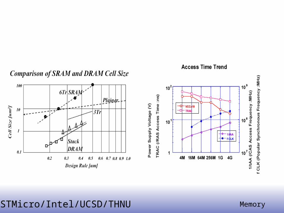
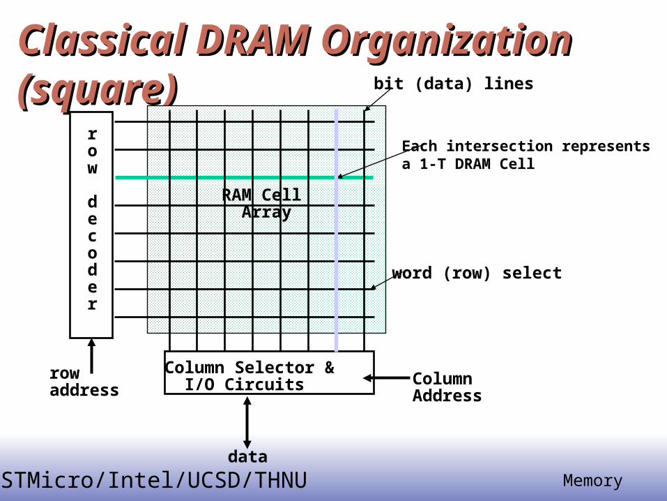
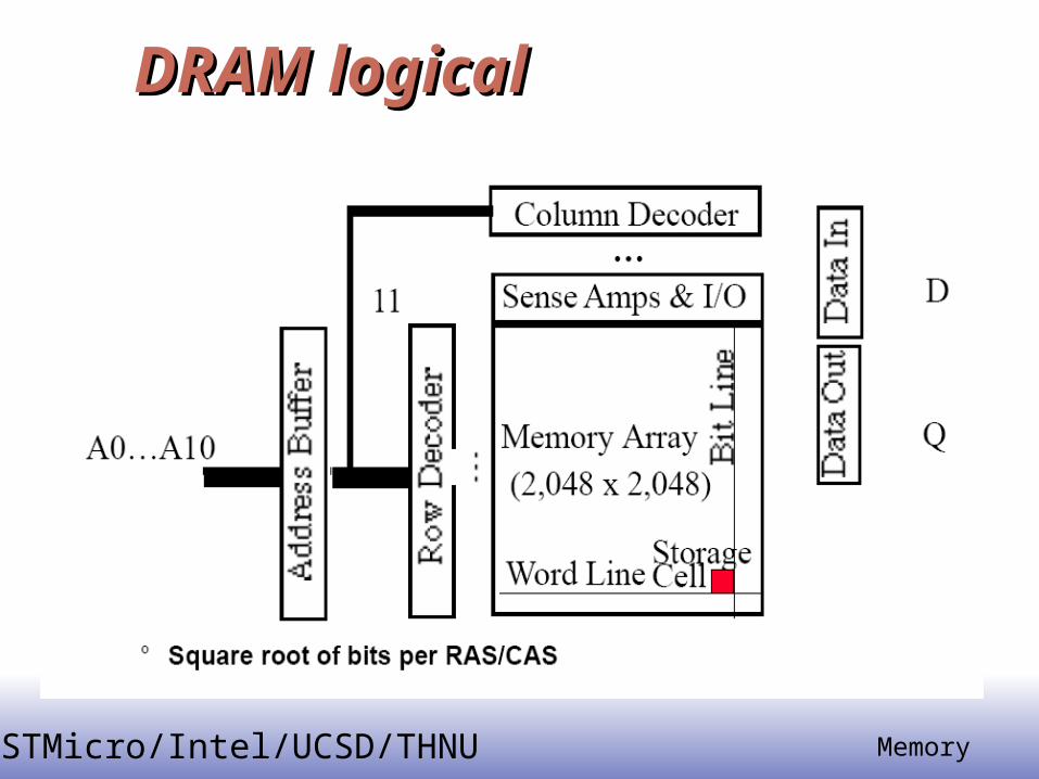
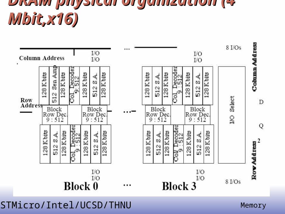
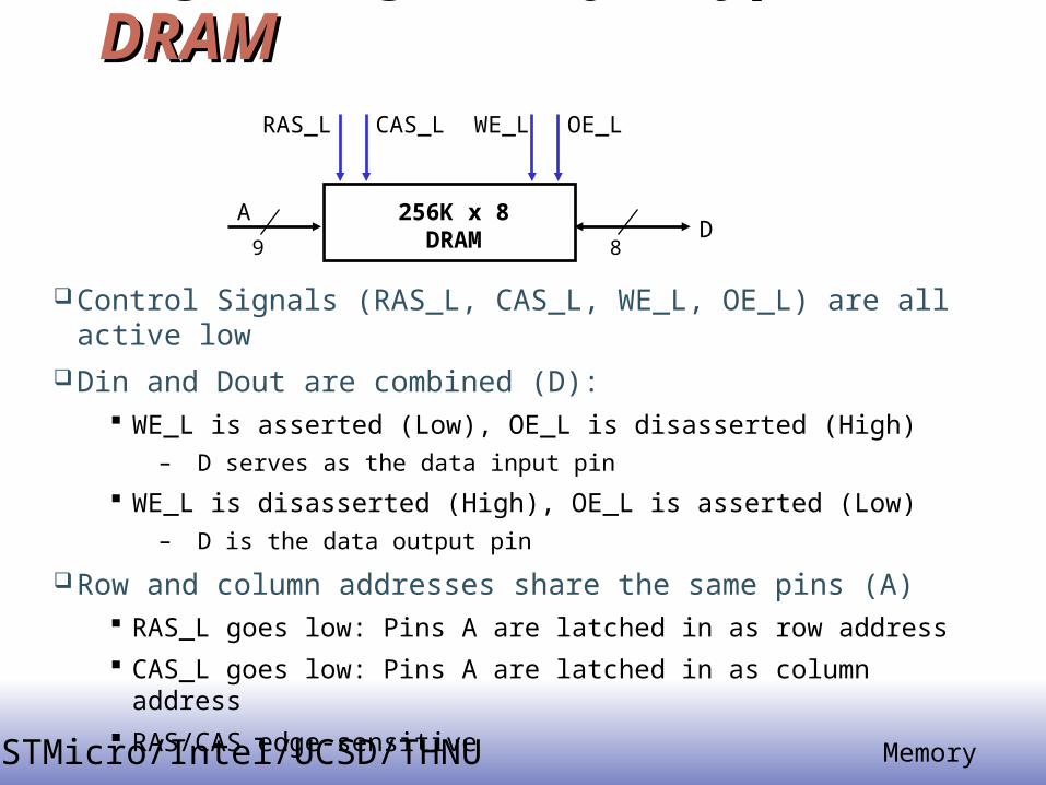
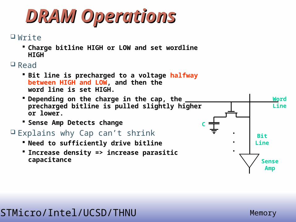
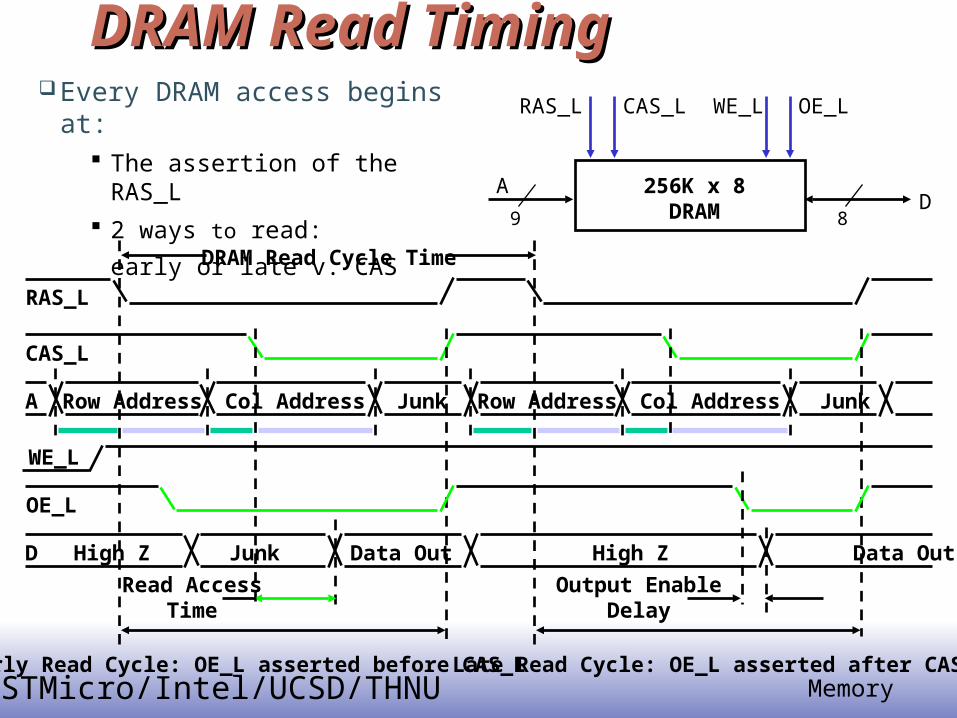
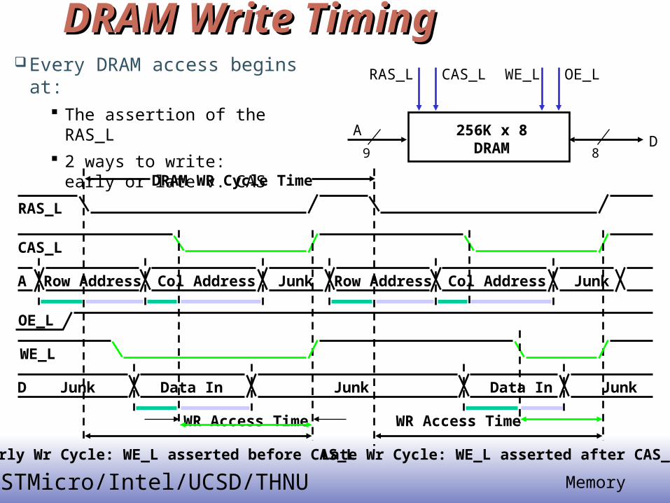
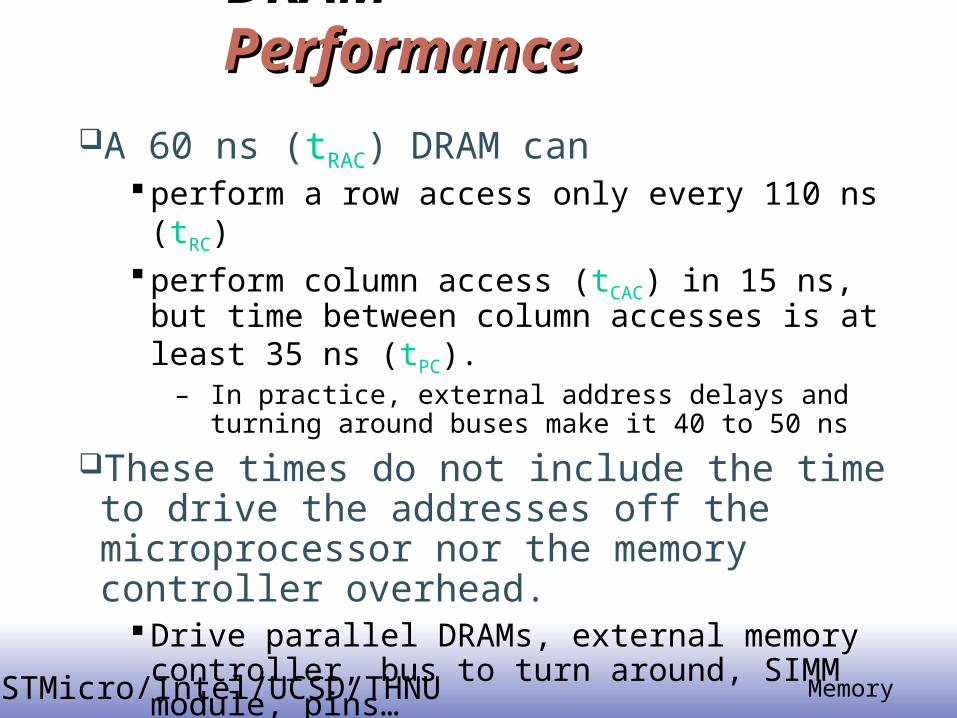
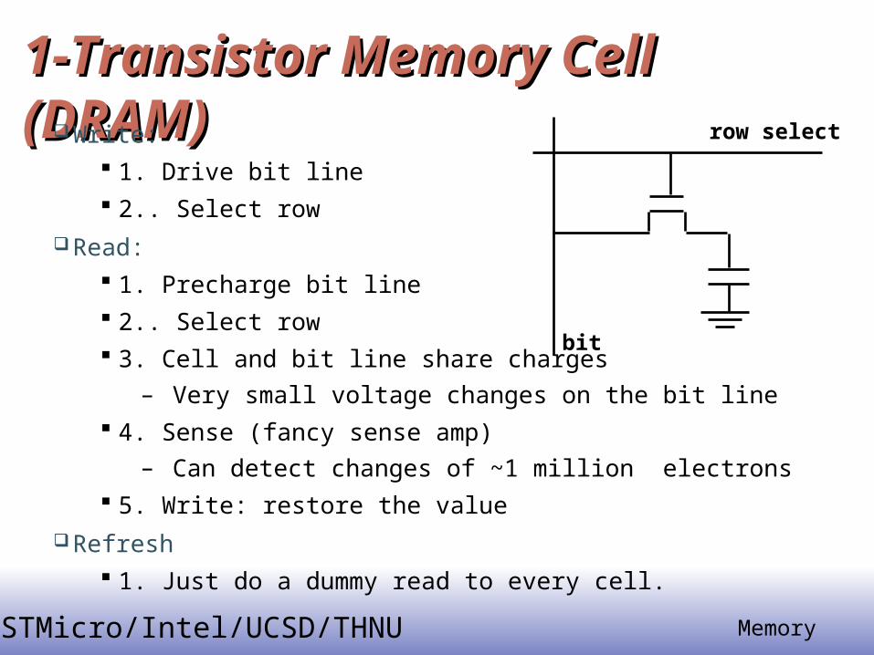
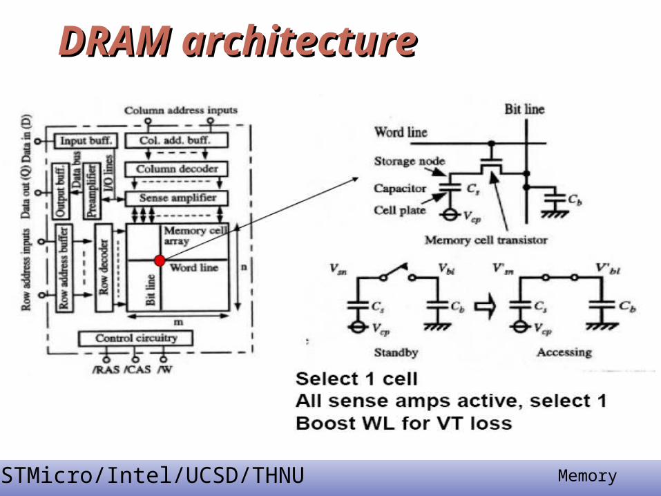
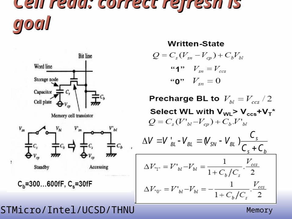
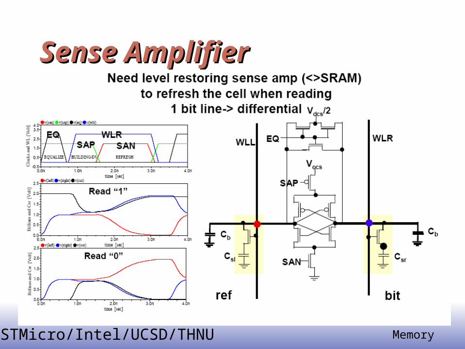
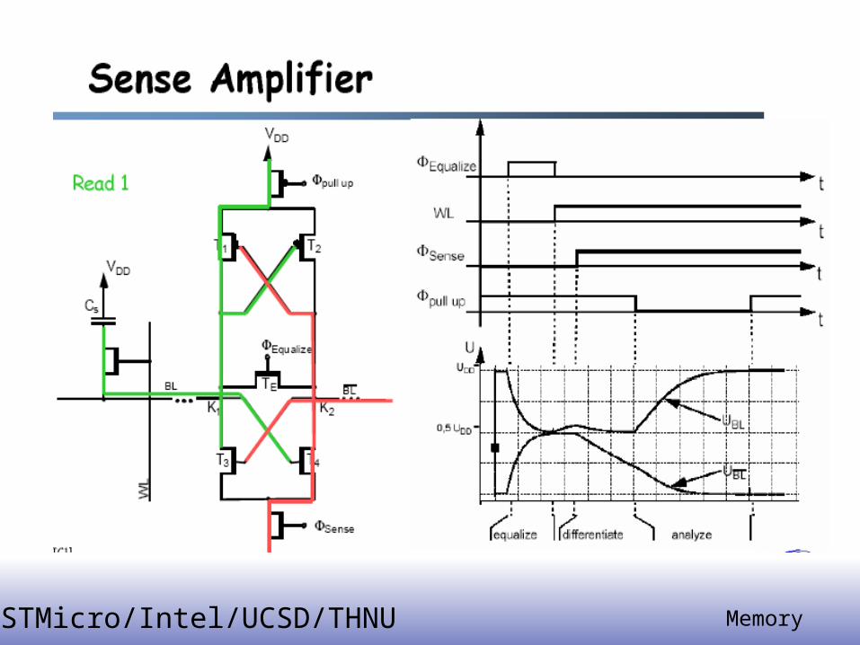
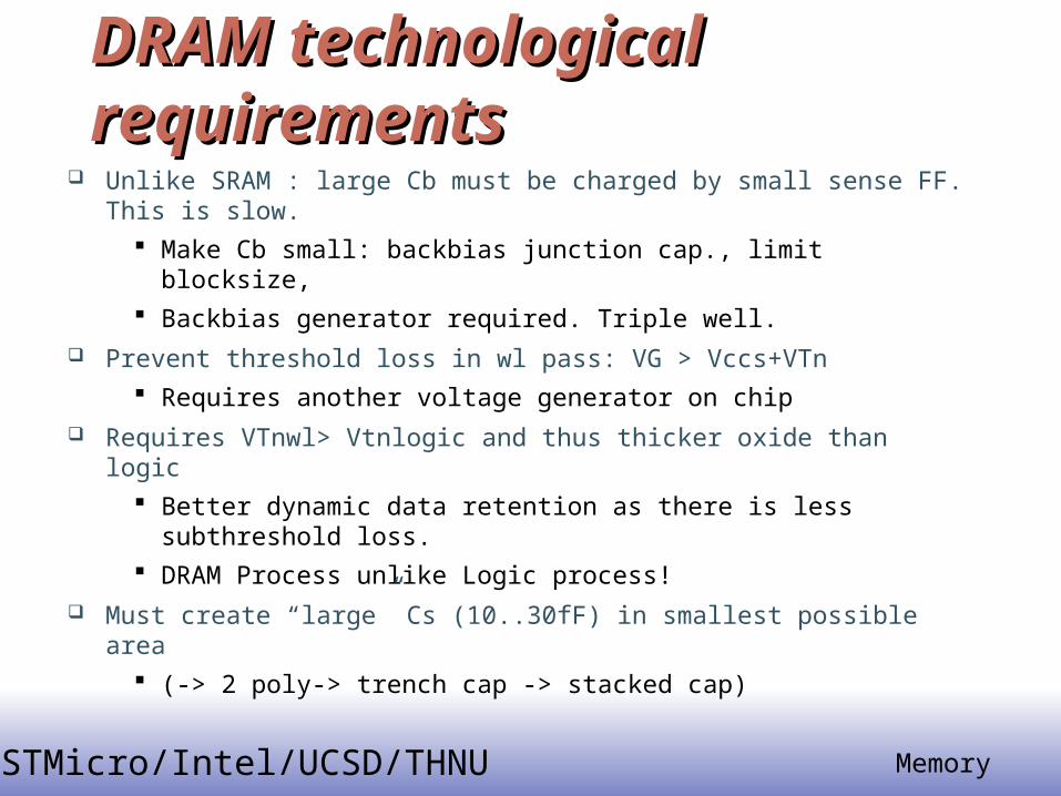
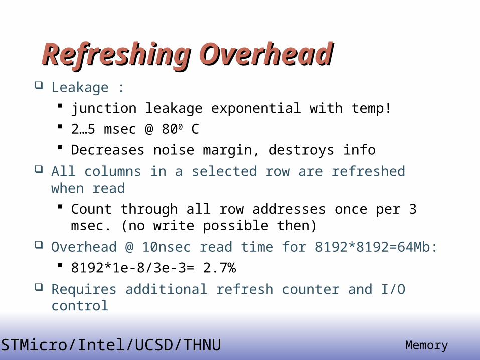
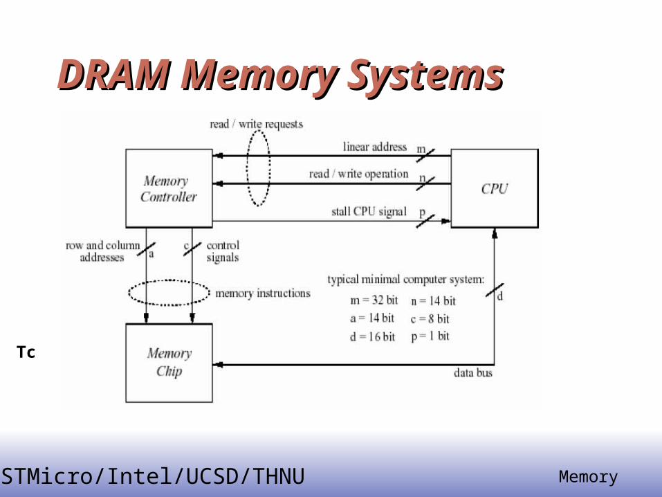
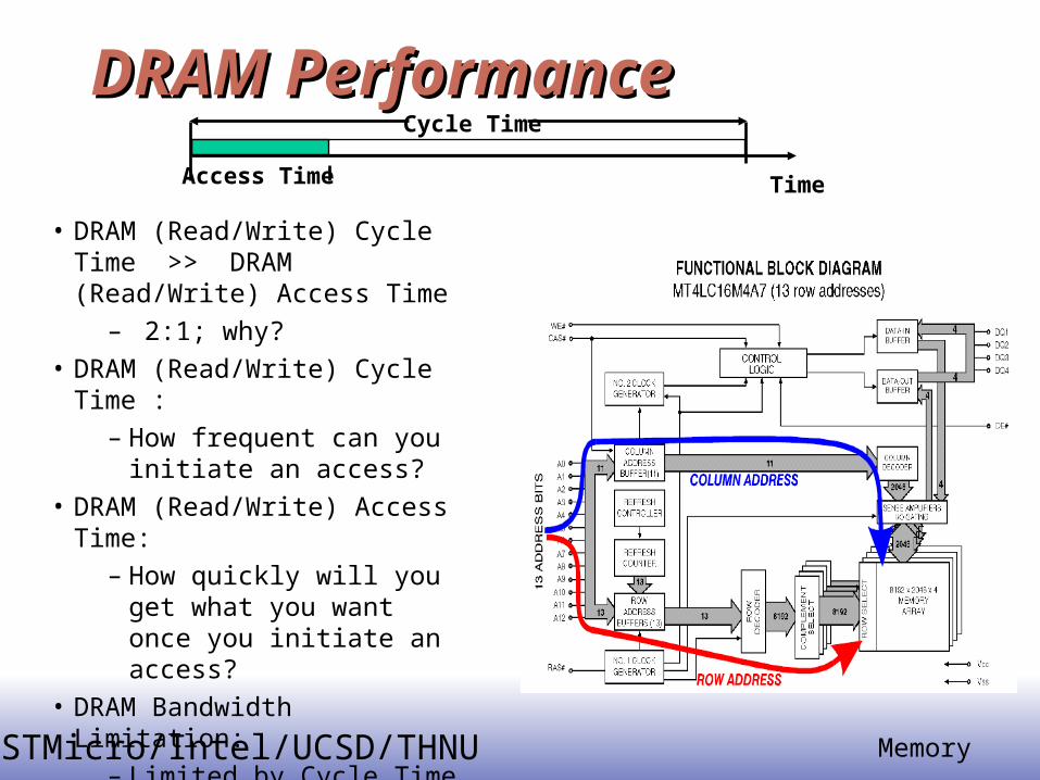
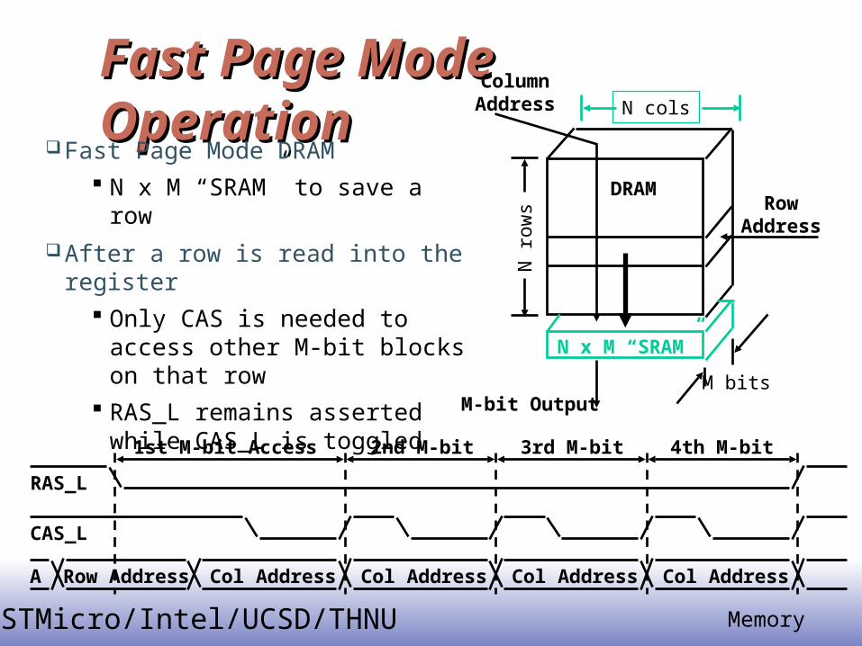
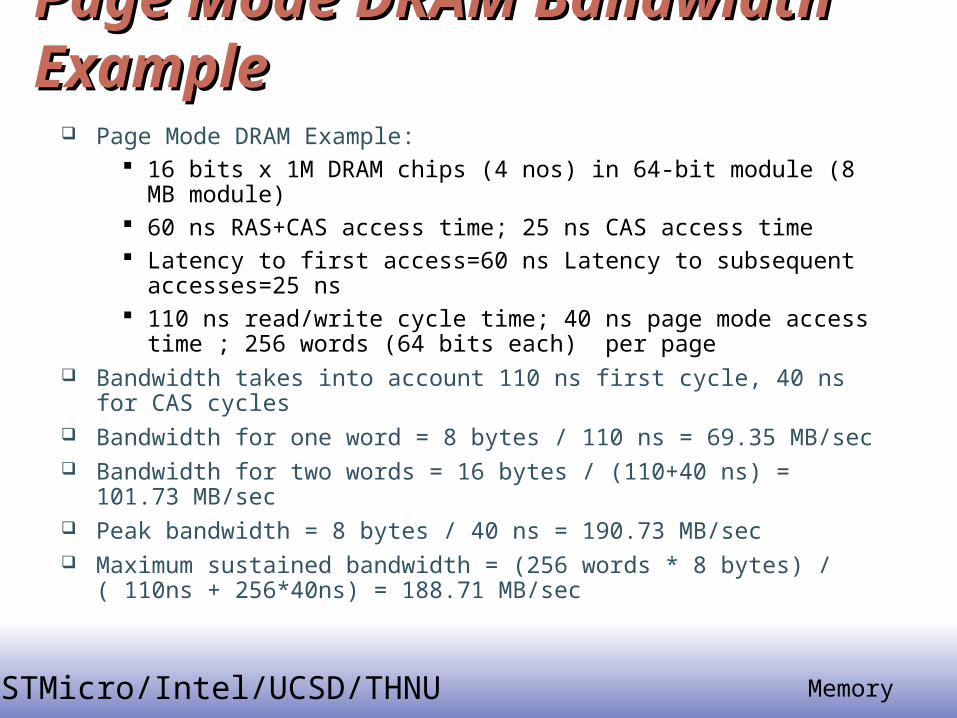
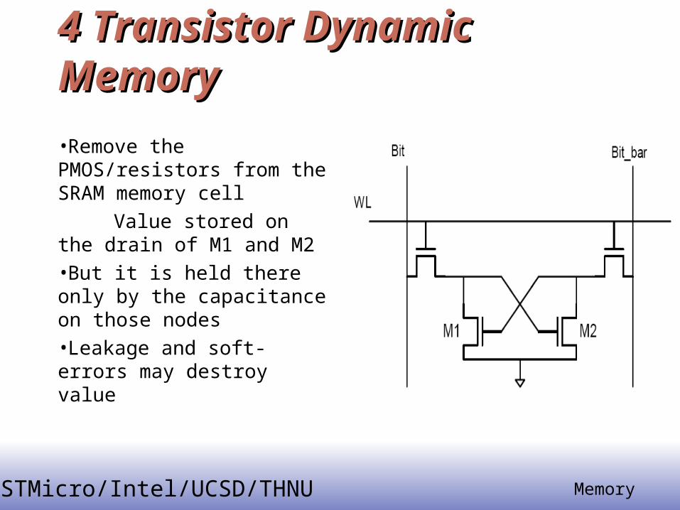
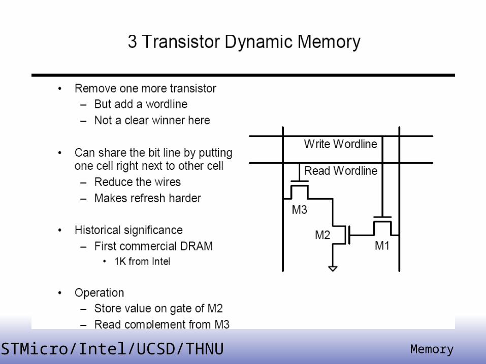
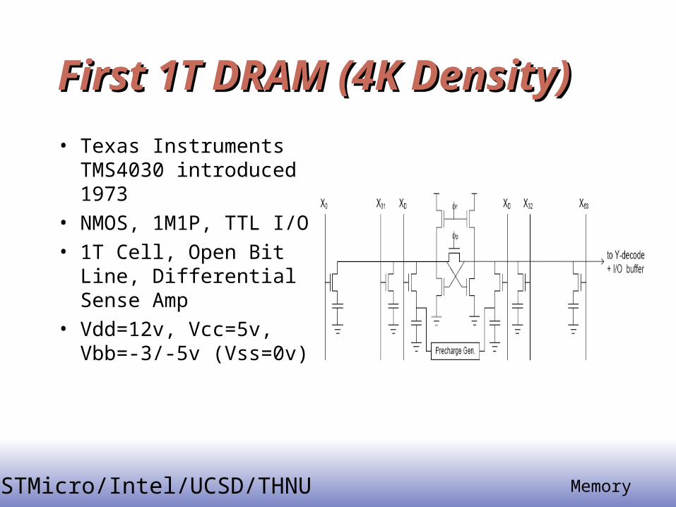
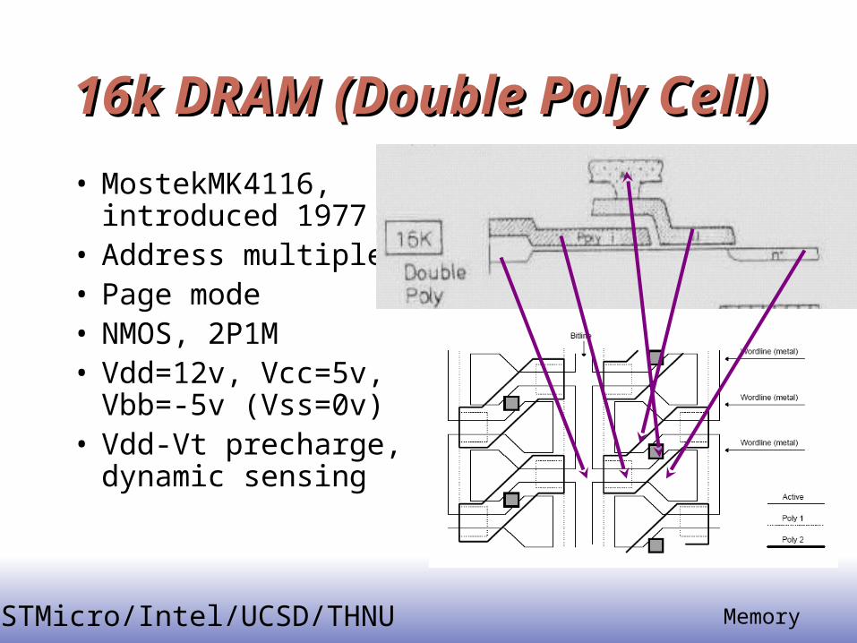
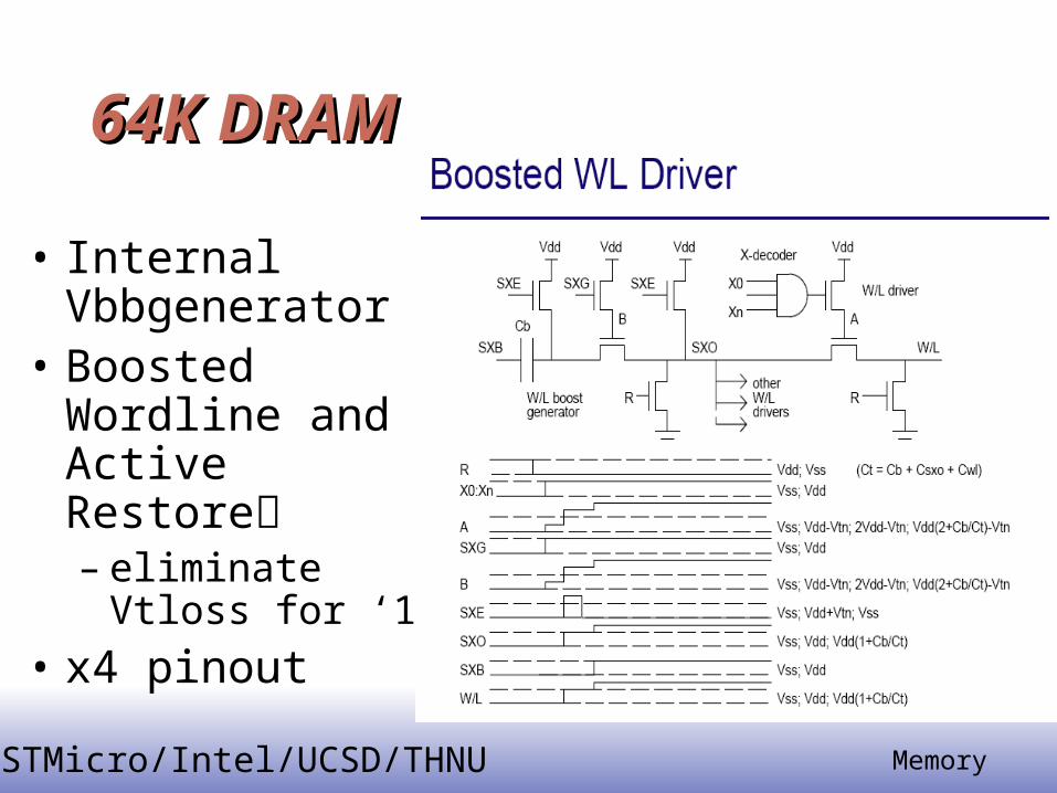
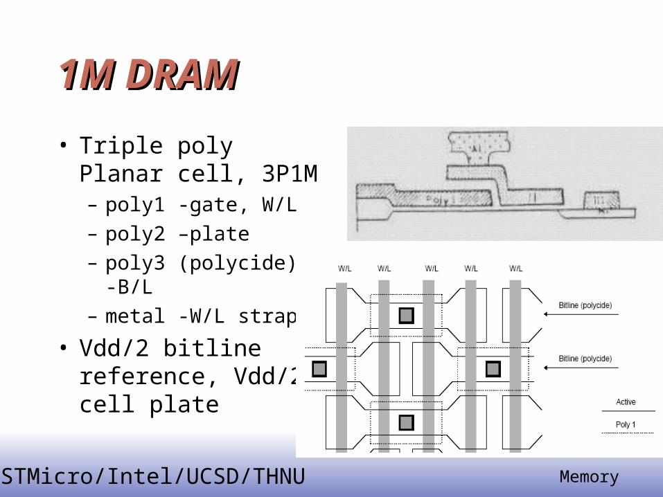
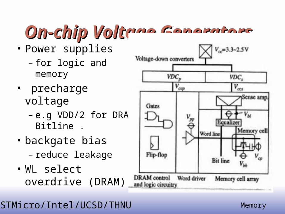
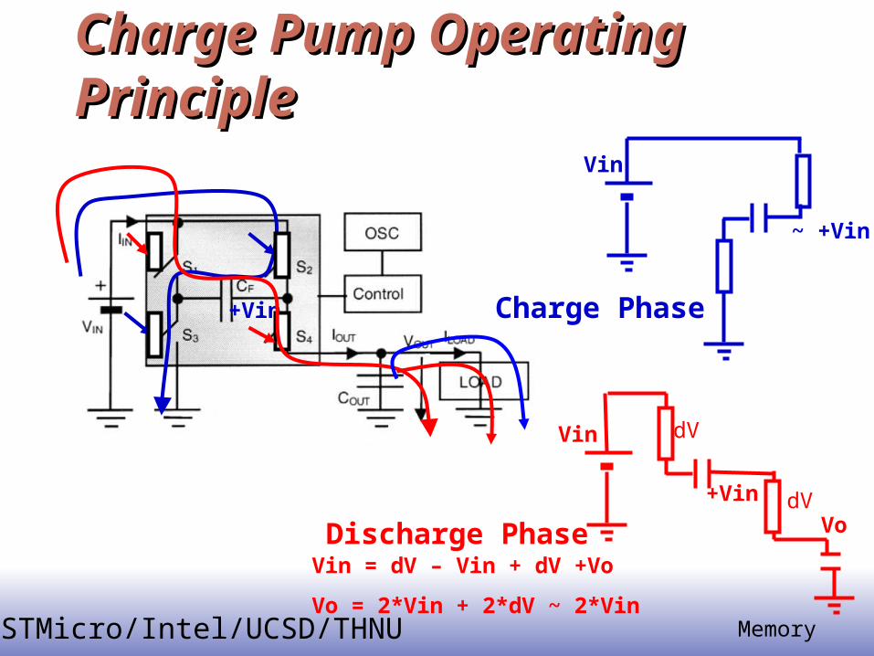
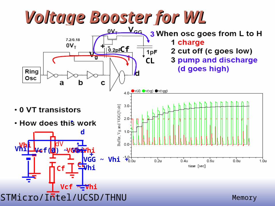
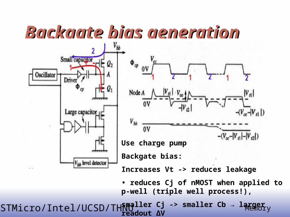
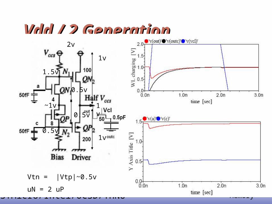
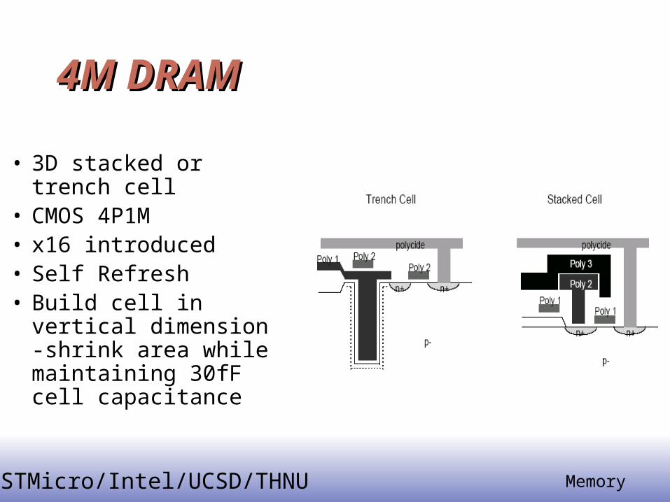
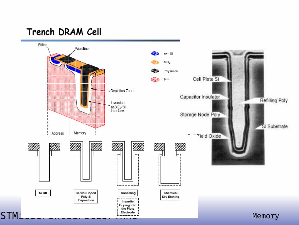
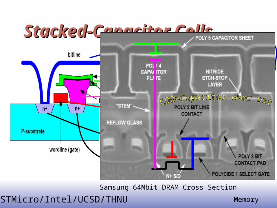
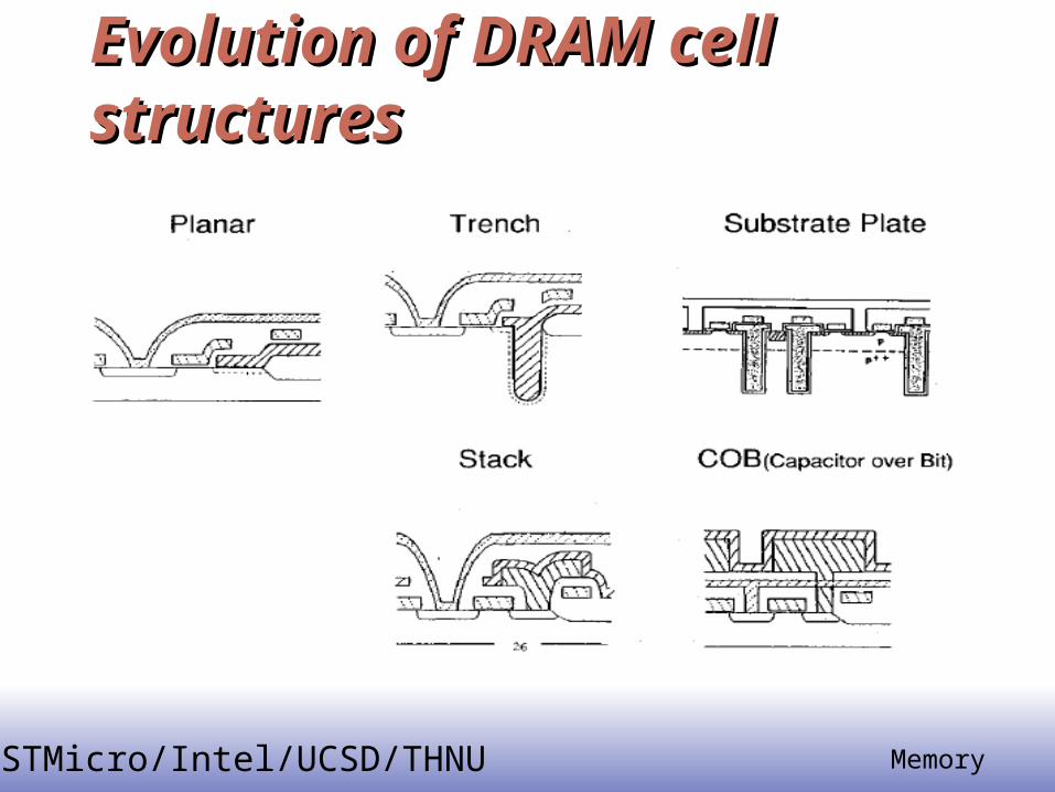
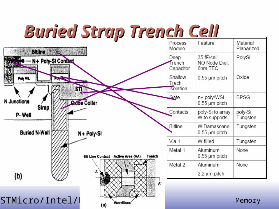
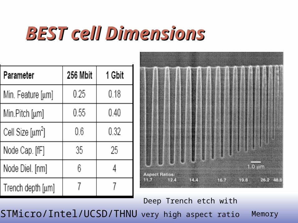
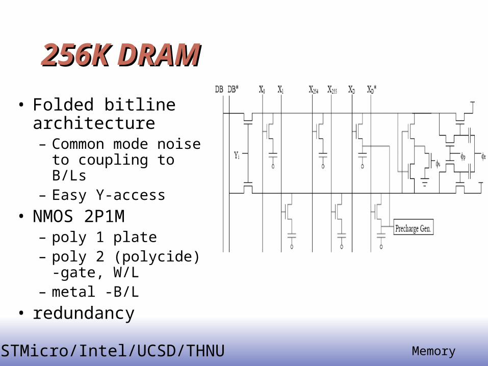
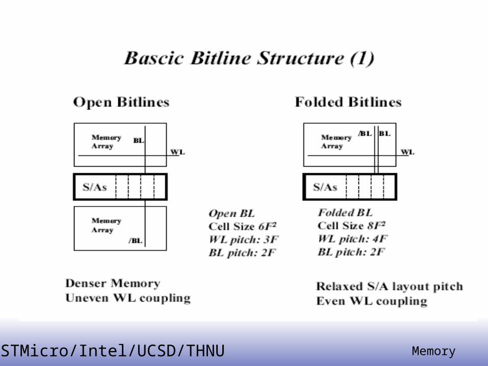
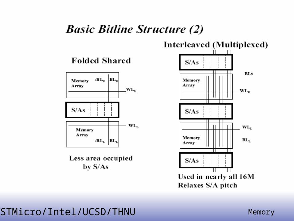
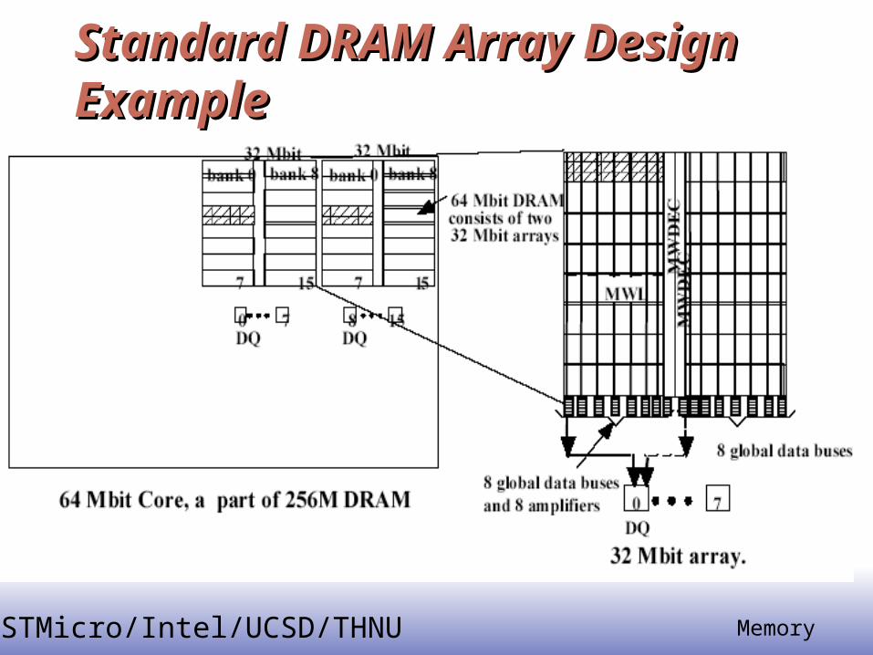
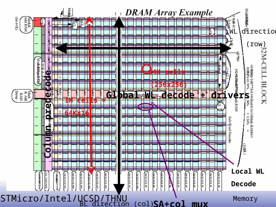
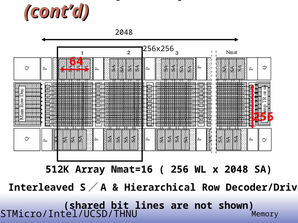
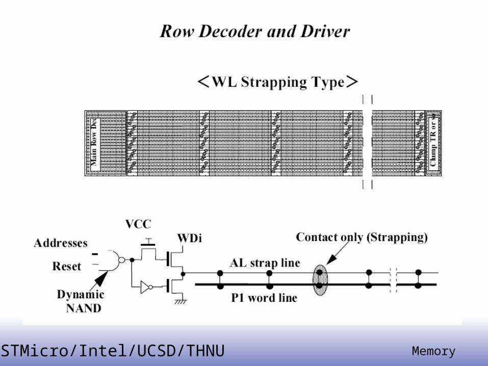
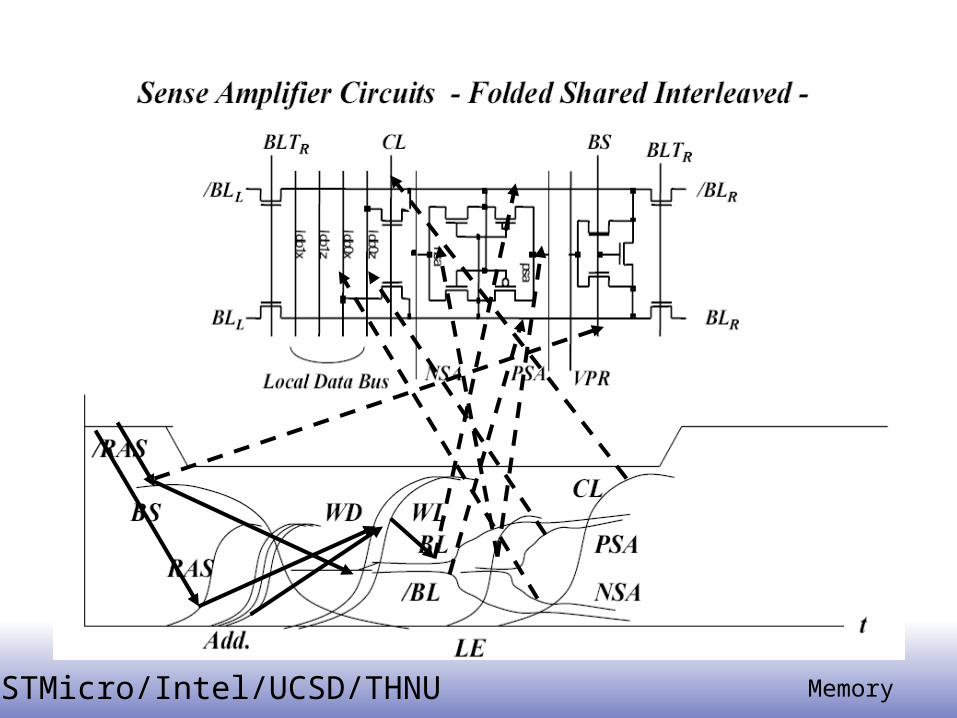
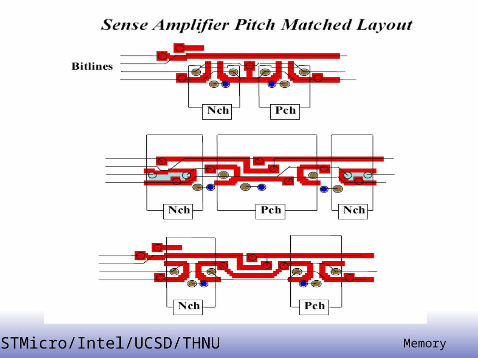
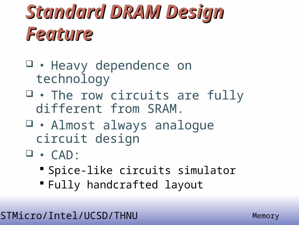
EE14154
MemorySTMicroIntelUCSDTHNU
Standard DRAM Design FeatureStandard DRAM Design Feature
Heavy dependence on technology The row circuits are fully different
from SRAM Almost always analogue circuit
design CAD
Spice-like circuits simulator Fully handcrafted layout