Embed Size (px)
Citation preview
EE141
1
EE141EECS141 1Lecture #18
EE141-Fall 2012Digital Integrated Circuits
Lecture 18Ratioed and Pass Transistor Logic
EE141EECS141 2Lecture #18
Announcements
Project #1 due Thursday
EE141EECS141 3Lecture #18
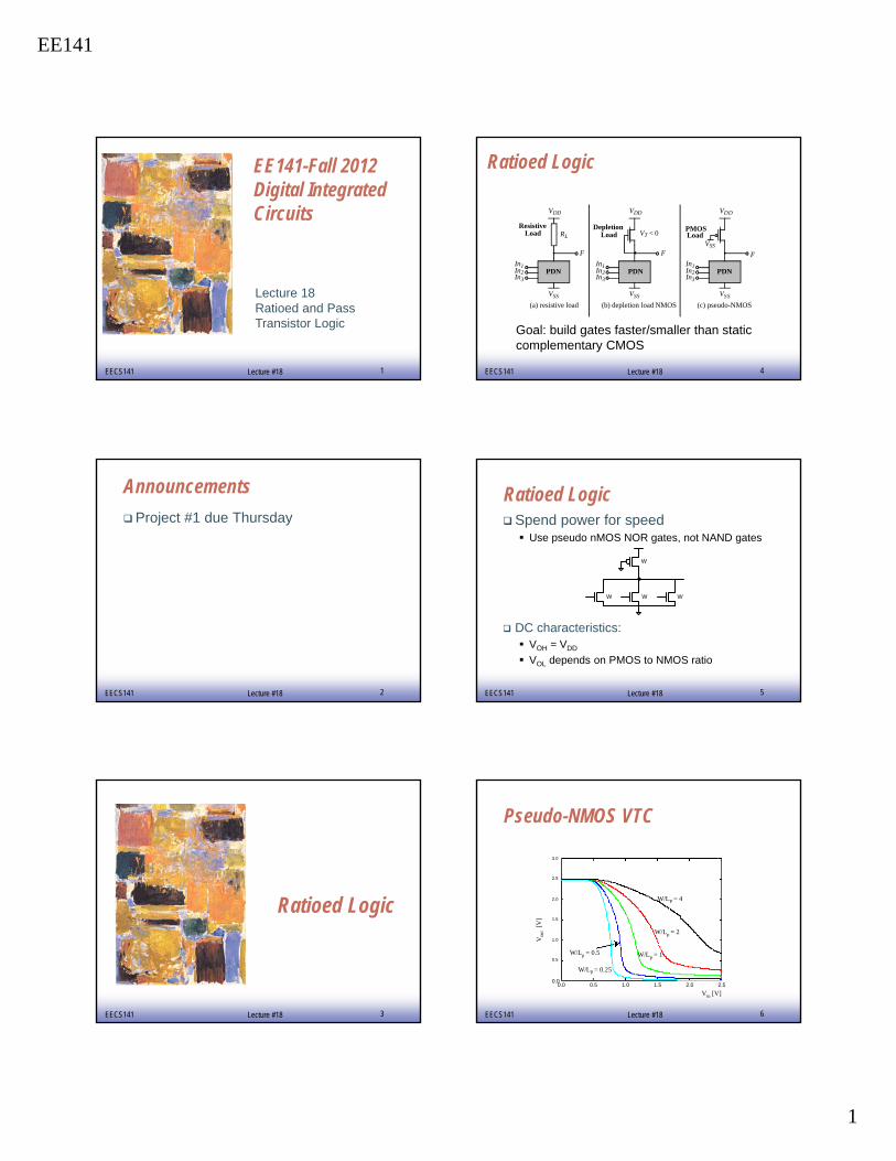
Ratioed Logic
EE141EECS141 4Lecture #18
Ratioed Logic
VDD
VSS
PDNIn1In2In3
F
RLLoad
VDD
VSS
In1In2In3
F
VDD
VSS
PDNIn1In2In3
F
VSS
PDN
Resistive DepletionLoad
PMOSLoad
(a) resistive load (b) depletion load NMOS (c) pseudo-NMOS
VT < 0
Goal: build gates faster/smaller than staticcomplementary CMOS
EE141EECS141 5Lecture #18
Ratioed LogicSpend power for speed Use pseudo nMOS NOR gates, not NAND gates
DC characteristics: VOH = VDD
VOL depends on PMOS to NMOS ratio
W
WW W
EE141EECS141 6Lecture #18
Pseudo-NMOS VTC
0.0 0.5 1.0 1.5 2.0 2.50.0
0.5
1.0
1.5
2.0
2.5
3.0
Vin [V]
Vou
t[V
]
W/Lp = 4
W/Lp = 2
W/Lp = 1
W/Lp = 0.25
W/Lp = 0.5

EE141
2
EE141EECS141 7Lecture #18
Ratioed Logic LE Rising and falling delays aren’t the same
Calculate LE for the two edges separately
For tpLH: Cgate = WCG Cinv = (3/2)WCG LELH =
EE141EECS141 8Lecture #18
Ratioed Logic LE (pull-down edge)
What is LE for tpHL?
Switch model would predict Reff = Rn||Rp
Would that give the right answer for LE?
EE141EECS141 9Lecture #18
Response on Falling Edge
Time constant is smaller, but it takes more time to complete 50% VDD transient. Rp actually takes some current away from
discharging C
Rp
Rn C
vo(t)
0 1 2 3 40
0.5
1
vo(t)/VDD
t
Rp=Rn
Rp=2Rn
Rp=4Rn
Rp=
CRpRn
RpRn
/1)( t
DD
o eRpRn
Rn
RpRn
Rn
V
tv
EE141EECS141 10Lecture #18
Ratioed Logic Pull-down Delay Think in terms of the current driving Cload
When you have a conflict between currents Available current is the difference between the two
In pseudo-nMOS case:
(Works because Rp >> Rn for good noise margin)
1drive drive
1 RnR = R =
1 1- Rn-Rn Rp Rp
EE141EECS141 11Lecture #18
Ratioed Logic LE (pull-down edge)
For tpHL (assuming Rsqp = 2Rsqn): Rgate = Rn/(1-Rn/Rp) = 2Rn Rinv = Rn
Cgate = WCG Cinv = 3WCG
LEHL =
LE is lower than an inverter! But have static power dissipation…
W
WW W
2W
W
EE141EECS141 12Lecture #18
Improved Loads (2)
VDD
VSS
F
Out
VDD
VSS
F_b
Out
AABB
M1 M2
Differential Cascode Voltage Switch Logic (DCVSL)
EE141
3
EE141EECS141 13Lecture #18
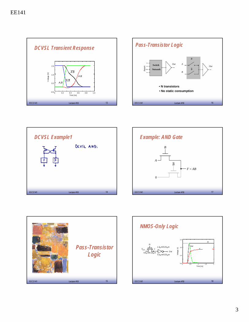
DCVSL Transient Response
0 0.2 0.4 0.6 0.8 1.0-0.5
0.5
1.5
2.5
Time [ns]
Vol
tage
[V] A B
A B
A,BA,B
EE141EECS141 14Lecture #18
DCVSL Example1
EE141EECS141 15Lecture #18
Pass-TransistorLogic
EE141EECS141 16Lecture #18
Pass-Transistor Logic
Inpu
ts
Switch
Network
OutOut
A
B
B
B
• N transistors
• No static consumption
EE141EECS141 17Lecture #18
Example: AND Gate
B
B
A
F = AB
0
EE141EECS141 18Lecture #18
NMOS-Only Logic
VDD
In
Outx
0.5m/0.25m0.5m/0.25m
1.5m/0.25m
0 0.5 1 1.5 20.0
1.0
2.0
3.0
Time [ns]
Vo
ltage
[V]
xOut
In
EE141
4
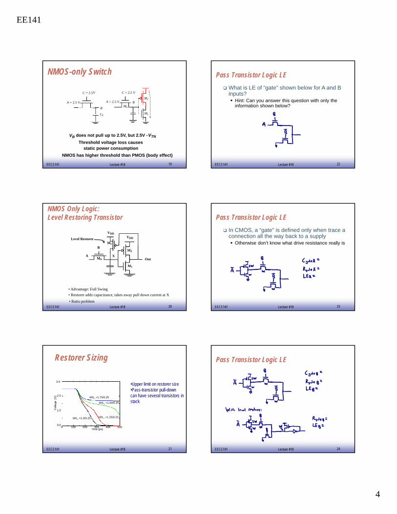
EE141EECS141 19Lecture #18
NMOS-only Switch
A = 2.5 V
B
C = 2.5V
CL
A = 2.5 V
C = 2.5 V
BM2
M1
Mn
Threshold voltage loss causesstatic power consumption
VB does not pull up to 2.5V, but 2.5V -VTN
NMOS has higher threshold than PMOS (body effect)
EE141EECS141 20Lecture #18
NMOS Only Logic: Level Restoring Transistor
M2
M1
Mn
Mr
OutA
B
VDDVDDLevel Restorer
X
• Advantage: Full Swing
• Restorer adds capacitance, takes away pull down current at X
• Ratio problem
EE141EECS141 21Lecture #18
Restorer Sizing
0 100 200 300 400 5000.0
1.0
2.0
W/Lr =1.0/0.25 W/Lr =1.25/0.25
W/Lr =1.50/0.25
W/Lr =1.75/0.25
Vol
tage
[V]
Time [ps]
3.0•Upper limit on restorer size•Pass-transistor pull-downcan have several transistors in stack
EE141EECS141 22Lecture #18
Pass Transistor Logic LE
What is LE of “gate” shown below for A and B inputs? Hint: Can you answer this question with only the
information shown below?
EE141EECS141 23Lecture #18
Pass Transistor Logic LE
In CMOS, a “gate” is defined only when trace a connection all the way back to a supply Otherwise don’t know what drive resistance really is
EE141EECS141 24Lecture #18
Pass Transistor Logic LE
EE141
5
EE141EECS141 25Lecture #18
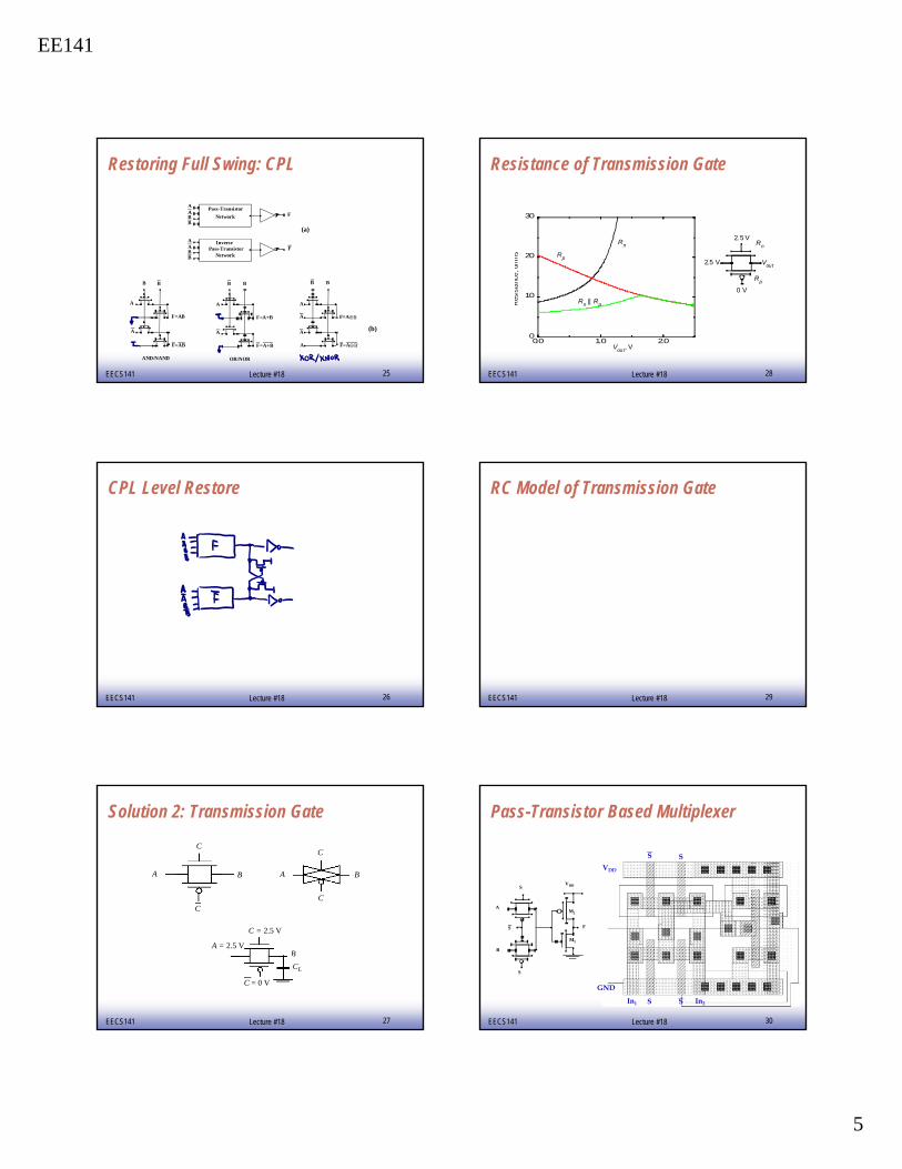
Restoring Full Swing: CPL
A
B
A
B
B B B B
A
B
A
B
F=AB
F=AB
F=A+B
F=A+B
B B
A
A
A
A
F=AÝ
F=AÝ
OR/NOR EXOR/NEXORAND/NAND
F
F
Pass-Transistor
Network
Pass-TransistorNetwork
AABB
AABB
Inverse
(a)
(b)
EE141EECS141 26Lecture #18
CPL Level Restore
EE141EECS141 27Lecture #18
Solution 2: Transmission Gate
A B
C
C
A B
C
C
B
CL
C = 0 V
A = 2.5 V
C = 2.5 V
EE141EECS141 28Lecture #18
Resistance of Transmission Gate
Vout
0 V
2.5 V
2.5 VRn
Rp
0.0 1.0 2.00
10
20
30
Vout, V
Res
ista
nce
, oh
ms
Rn
Rp
Rn || Rp
EE141EECS141 29Lecture #18
RC Model of Transmission Gate
EE141EECS141 30Lecture #18
Pass-Transistor Based Multiplexer
AM2
M1
B
S
S
S F
VDD
GND
VDD
In1 In2S S
S S
EE141
6
EE141EECS141 31Lecture #18
Next Lecture
Dynamic Logic