Embed Size (px)
Citation preview

EE213 L01 From Architecture to Layout.1 Pingqiang, ShanghaiTech, 2017
EE213Digital Integrated Circuits II
Lecture 01: From Architecture to Layout
Prof. Pingqiang Zhou
Chapte
r 1
Chapte
r 4

EE213 L01 From Architecture to Layout.2 Pingqiang, ShanghaiTech, 2017
Coping with Complexity
How to design System-on-Chip or Microprocessor?
Many millions (even billions!) of transistors
Tens to hundreds of engineers
https://en.wikipedia.org/wiki/Atom_(system_on_chip)
The Core i7 die and major components.
http://techreport.com/review/15818/intel-core-i7-processors
Microcontroller-based system on a chip

EE213 L01 From Architecture to Layout.3 Pingqiang, ShanghaiTech, 2017
Structured Design
Hierarchy: Divide and Conquer
Recursively system into modules
Regularity
Reuse modules wherever possible
Ex: Standard cell library
Modularity: well-formed interfaces
Allows modules to be treated as black boxes
Locality
Physical and temporal

EE213 L01 From Architecture to Layout.4 Pingqiang, ShanghaiTech, 2017
Design Abstraction Levels
SYSTEM
GATE
CIRCUIT
VoutVin
CIRCUIT
VoutVin
MODULE
+
DEVICE
n+
S D
n+
G

EE213 L01 From Architecture to Layout.5 Pingqiang, ShanghaiTech, 2017
Design Abstractions
Architecture: User’s perspective, what does it do?
Instruction set, registers
MIPS, x86, Alpha, PIC, ARM, …
Microarchitecture
Single cycle/multicycle, pipelined, superscalar?
Ex: 80386, 80486, Pentium, Atom, AMD, Phenom, …
Logic: how are functional blocks constructed
Ripple carry, carry lookahead, carry select adders
Circuit: how are transistors used
Complementary CMOS, pass transistors, domino
Physical: chip layout
Objects: datapaths, memories, random logic

EE213 L01 From Architecture to Layout.6 Pingqiang, ShanghaiTech, 2017
Gajski Y-Chart

EE213 L01 From Architecture to Layout.7 Pingqiang, ShanghaiTech, 2017
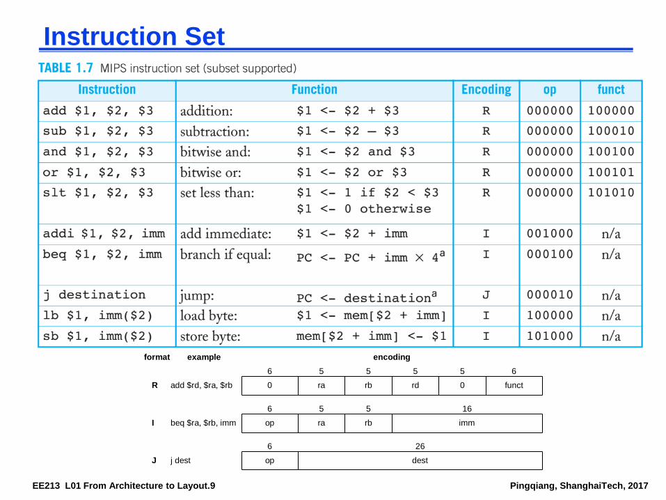
MIPS Processor - An Example

EE213 L01 From Architecture to Layout.8 Pingqiang, ShanghaiTech, 2017
1 - (MIPS) Architecture (Simple 32-bit RISC)
Example: subset of MIPS processor architecture
Drawn from Patterson & Hennessy, chapter 4
Consider 8-bit subset using 8-bit datapath
Only implement 8 registers ($0 - $7)
$0 hardwired to 00000000
8-bit program counter
Interested in RISC? See
http://baike.baidu.com/view/736344.htm
EE213 L01 From Architecture to Layout.9 Pingqiang, ShanghaiTech, 2017
Instruction Set
format example encoding
R
I
J
0 ra rb rd 0 funct
op
op
ra rb imm
6
6
6
65 5 5 5
5 5 16
26
add $rd, $ra, $rb
beq $ra, $rb, imm
j dest dest

EE213 L01 From Architecture to Layout.10 Pingqiang, ShanghaiTech, 2017
Fibonacci (in C Language)
f0 = 1; f-1 = -1
fn = fn-1 + fn-2
f = 1, 1, 2, 3, 5, 8, 13, …

EE213 L01 From Architecture to Layout.11 Pingqiang, ShanghaiTech, 2017
Fibonacci (in Assembly Language)

EE213 L01 From Architecture to Layout.12 Pingqiang, ShanghaiTech, 2017
Fibonacci (in Binary Code)
1st statement: addi $3, $0, 8. How do we translate this to machine language?
format example encoding
R
I
J
0 ra rb rd 0 funct
op
op
ra rb imm
6
6
6
65 5 5 5
5 5 16
26
add $rd, $ra, $rb
beq $ra, $rb, imm
j dest dest

EE213 L01 From Architecture to Layout.13 Pingqiang, ShanghaiTech, 2017
Fibonacci (in Binary Code)
Machine language program

EE213 L01 From Architecture to Layout.14 Pingqiang, ShanghaiTech, 2017
2 - (MIPS) Microarchitecture
Multicycle marchitecture

EE213 L01 From Architecture to Layout.15 Pingqiang, ShanghaiTech, 2017
Multicycle Controller

EE213 L01 From Architecture to Layout.16 Pingqiang, ShanghaiTech, 2017
ALU Decoder Unit

EE213 L01 From Architecture to Layout.17 Pingqiang, ShanghaiTech, 2017
3 - (MIPS) Logic Design
Start at top level
Hierarchically decompose MIPS into units
Top-level interface
reset
ph1
ph2
crystal
oscillator
2-phase
clock
generator MIPS
processor adr
writedata
memdata
external
memory
memreadmemwrite
8
8
8
EE213 L01 From Architecture to Layout.18 Pingqiang, ShanghaiTech, 2017
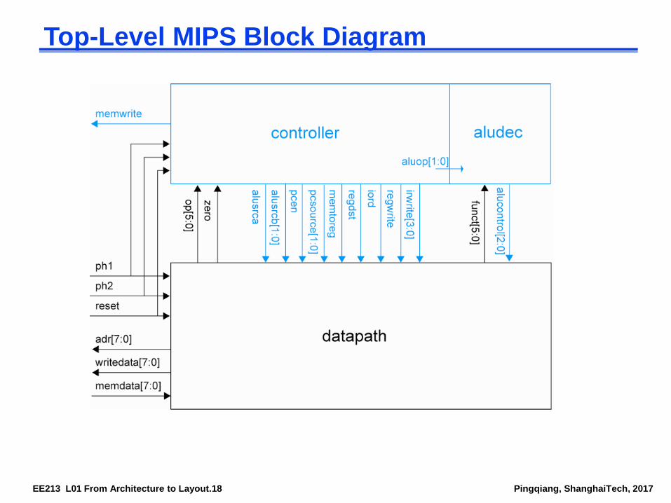
Top-Level MIPS Block Diagram

EE213 L01 From Architecture to Layout.19 Pingqiang, ShanghaiTech, 2017
Hierarchical Design
mips
controller alucontrol datapath
standard
cell librarybitslice zipper
alu
and2
flopinv4x
mux2
mux4
ramslice
fulladder
nand2nor2
or2
inv
tri

EE213 L01 From Architecture to Layout.20 Pingqiang, ShanghaiTech, 2017
HDLs
Hardware Description Languages
Widely used in logic design
Verilog and VHDL
Describe hardware using code
Document logic functions
Simulate logic before building
Synthesize code into gates and layout
- Requires a library of standard cells

EE213 L01 From Architecture to Layout.21 Pingqiang, ShanghaiTech, 2017
Verilog Example – Full Addermips
controller alucontrol datapath
standard
cell librarybitslice zipper
alu
and2
flopinv4x
mux2
mux4
ramslice
fulladder
nand2nor2
or2
inv
tri
8-Bit Adder in ALU

EE213 L01 From Architecture to Layout.22 Pingqiang, ShanghaiTech, 2017
Verilog Example – Full Adder
module fulladder(input a, b, c,
output s, cout);
sum s1(a, b, c, s);
carry c1(a, b, c, cout);
endmodule
module carry(input a, b, c,
output cout)
assign cout = (a&b) | (a&c) | (b&c);
endmodule

EE213 L01 From Architecture to Layout.23 Pingqiang, ShanghaiTech, 2017
4 – (MIPS) Circuit Design
Circuit design is concerned with arranging transistors to perform a particular logic function.
How should logic be implemented?
NANDs and NORs vs. ANDs and ORs?
Fan-in and fan-out?
How wide should transistors be?
These choices affect speed, area, power
Logic synthesis makes these choices for you
Good enough for many applications
Hand-crafted circuits are still better

EE213 L01 From Architecture to Layout.24 Pingqiang, ShanghaiTech, 2017
Transistors as Switches
Can view MOS transistors as electrically-controlled switches
g
s
d
g = 0
s
d
g = 1
s
d
g
s
d
s
d
s
d
nMOS
pMOS
OFFON
ONOFF
n+
p
GateSource Drain
bulk Si
SiO2
Polysilicon
n+D
1
S
SiO2
n
GateSource Drain
bulk Si
Polysilicon
p+ p+

EE213 L01 From Architecture to Layout.25 Pingqiang, ShanghaiTech, 2017
0
VDD
A Y
GND
CMOS Inverter
A Y
0 1
1 0
A Y
OFF
ON 1
ON
OFF

EE213 L01 From Architecture to Layout.26 Pingqiang, ShanghaiTech, 2017
CMOS NAND Gate
A B Y
0 0 1
0 1 1
1 0 1
1 1 0
OFFOFF
ON
ON
1
1
OFFON
OFF
ON
0
1
ON OFF
ON
OFF
1
0
ON ON
OFF
OFF
0
0
A
B
Y

EE213 L01 From Architecture to Layout.27 Pingqiang, ShanghaiTech, 2017
Complementary CMOS
Complementary CMOS logic gates
nMOS pull-down network
pMOS pull-up network
a.k.a. static CMOS
pMOS
pull-up
network
output
inputs
nMOS
pull-down
network
Pull-up OFF Pull-up ON
Pull-down OFF Z (float) 1
Pull-down ON 0 X (crowbar)

EE213 L01 From Architecture to Layout.28 Pingqiang, ShanghaiTech, 2017
Series and Parallel
nMOS: 1 = ON
pMOS: 0 = ON
Series: both must be ON
Parallel: either can be ON
(a)
a
b
a
b
g1
g2
0
0
a
b
0
1
a
b
1
0
a
b
1
1
OFF OFF OFF ON
(b)
a
b
a
b
g1
g2
0
0
a
b
0
1
a
b
1
0
a
b
1
1
ON OFF OFF OFF
(c)
a
b
a
b
g1 g2 0 0
OFF ON ON ON
(d) ON ON ON OFF
a
b
0
a
b
1
a
b
11 0 1
a
b
0 0
a
b
0
a
b
1
a
b
11 0 1
a
b
g1 g2
EE213 L01 From Architecture to Layout.29 Pingqiang, ShanghaiTech, 2017
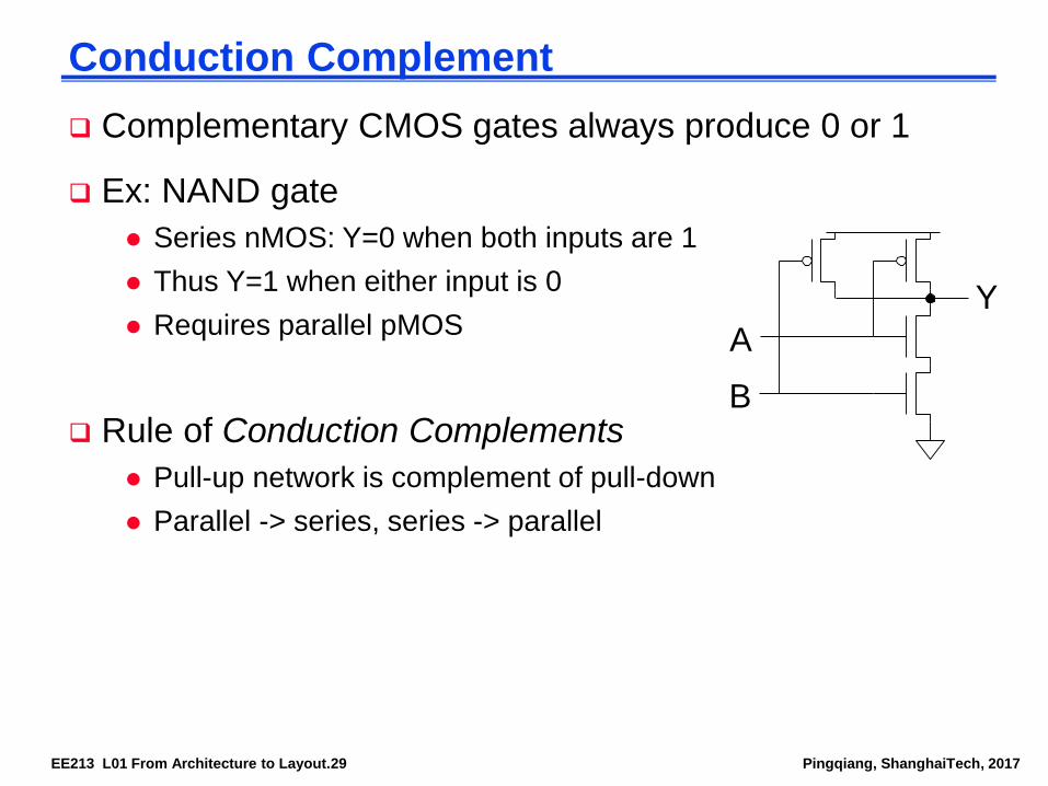
Conduction Complement
Complementary CMOS gates always produce 0 or 1
Ex: NAND gate
Series nMOS: Y=0 when both inputs are 1
Thus Y=1 when either input is 0
Requires parallel pMOS
Rule of Conduction Complements
Pull-up network is complement of pull-down
Parallel -> series, series -> parallel
A
B
Y

EE213 L01 From Architecture to Layout.30 Pingqiang, ShanghaiTech, 2017
CMOS NOR Gate
A B Y
0 0 1
0 1 0
1 0 0
1 1 0
A
BY

EE213 L01 From Architecture to Layout.31 Pingqiang, ShanghaiTech, 2017
Exercises - Compound Gates

EE213 L01 From Architecture to Layout.32 Pingqiang, ShanghaiTech, 2017
Example: Carry Logic
assign cout = (a&b) | (a&c) | (b&c);
ab
ac
bc
cout
x
y
z
g1
g2
g3
g4
Transistors? Gate Delays?
a b
c
c
a b
b
a
a
b
coutcn
n1 n2
n3
n4
n5 n6
p6p5
p4
p3
p2p1
i1
i3
i2
i4

EE213 L01 From Architecture to Layout.33 Pingqiang, ShanghaiTech, 2017
Gate-level Netlist
module carry(input a, b, c,
output cout)
wire x, y, z;
and g1(x, a, b);
and g2(y, a, c);
and g3(z, b, c);
or g4(cout, x, y, z);
endmodule
ab
ac
bc
cout
x
y
z
g1
g2
g3
g4
This is a technology-independent structural description,
because generic gates have been used and the actual
gate implementations have not been specified.

EE213 L01 From Architecture to Layout.34 Pingqiang, ShanghaiTech, 2017
Transistor-Level Netlist
a b
c
c
a b
b
a
a
b
coutcn
n1 n2
n3
n4
n5 n6
p6p5
p4
p3
p2p1
i1
i3
i2
i4
module carry(input a, b, c,
output cout)
wire i1, i2, i3, i4, cn;
tranif1 n1(i1, 0, a);
tranif1 n2(i1, 0, b);
tranif1 n3(cn, i1, c);
tranif1 n4(i2, 0, b);
tranif1 n5(cn, i2, a);
tranif0 p1(i3, 1, a);
tranif0 p2(i3, 1, b);
tranif0 p3(cn, i3, c);
tranif0 p4(i4, 1, b);
tranif0 p5(cn, i4, a);
tranif1 n6(cout, 0, cn);
tranif0 p6(cout, 1, cn);
endmodule
tranif1 corresponds to nMOS transistors that turn ON when the
gate is 1 while tranif0 corresponds to pMOS transistors that turn
ON when the gate is 0.

EE213 L01 From Architecture to Layout.35 Pingqiang, ShanghaiTech, 2017
SPICE Netlist.SUBCKT CARRY A B C COUT VDD GND
MN1 I1 A GND GND NMOS W=1U L=0.18U AD=0.3P AS=0.5P
MN2 I1 B GND GND NMOS W=1U L=0.18U AD=0.3P AS=0.5P
MN3 CN C I1 GND NMOS W=1U L=0.18U AD=0.5P AS=0.5P
MN4 I2 B GND GND NMOS W=1U L=0.18U AD=0.15P AS=0.5P
MN5 CN A I2 GND NMOS W=1U L=0.18U AD=0.5P AS=0.15P
MP1 I3 A VDD VDD PMOS W=2U L=0.18U AD=0.6P AS=1 P
MP2 I3 B VDD VDD PMOS W=2U L=0.18U AD=0.6P AS=1P
MP3 CN C I3 VDD PMOS W=2U L=0.18U AD=1P AS=1P
MP4 I4 B VDD VDD PMOS W=2U L=0.18U AD=0.3P AS=1P
MP5 CN A I4 VDD PMOS W=2U L=0.18U AD=1P AS=0.3P
MN6 COUT CN GND GND NMOS W=2U L=0.18U AD=1P AS=1P
MP6 COUT CN VDD VDD PMOS W=4U L=0.18U AD=2P AS=2P
CI1 I1 GND 2FF
CI3 I3 GND 3FF
CA A GND 4FF
CB B GND 4FF
CC C GND 2FF
CCN CN GND 4FF
CCOUT COUT GND 2FF
.ENDS
Transistors are specified by lines beginning with an M as follows:
Capacitors are specified by lines beginning with C as follows:
a b
c
c
a b
b
a
a
b
coutcn
n1 n2
n3
n4
n5 n6
p6p5
p4
p3
p2p1
i1
i3
i2
i4
EE213 L01 From Architecture to Layout.36 Pingqiang, ShanghaiTech, 2017
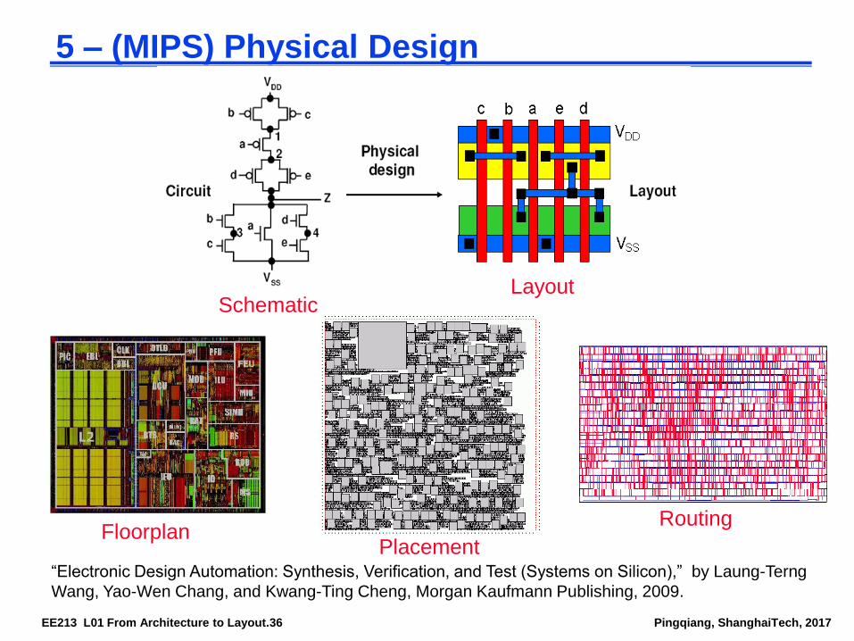
5 – (MIPS) Physical Design
FloorplanPlacement
Routing
SchematicLayout
“Electronic Design Automation: Synthesis, Verification, and Test (Systems on Silicon),” by Laung-Terng
Wang, Yao-Wen Chang, and Kwang-Ting Cheng, Morgan Kaufmann Publishing, 2009.

EE213 L01 From Architecture to Layout.37 Pingqiang, ShanghaiTech, 2017
MIPS Floorplan

EE213 L01 From Architecture to Layout.38 Pingqiang, ShanghaiTech, 2017
Standard Cells
Uniform cell height
Uniform well height
M1 VDD and GND rails
M2 Access to I/Os
Well/substrate taps
Exploits regularity

EE213 L01 From Architecture to Layout.39 Pingqiang, ShanghaiTech, 2017
Custom vs. Synthesis
8-bit Implementations

EE213 L01 From Architecture to Layout.40 Pingqiang, ShanghaiTech, 2017
Design Verification
Fabrication is slow & expensive
65 nm: $3M, a few months
Debugging chips is very hard
Limited visibility into operation
Prove design is right before building!
Logic simulation
Ckt. simulation/formal verification
Layout vs. schematic comparison
Design & electrical rule checks
Verification is > 50% of effort on most chips!
EE213 L01 From Architecture to Layout.41 Pingqiang, ShanghaiTech, 2017
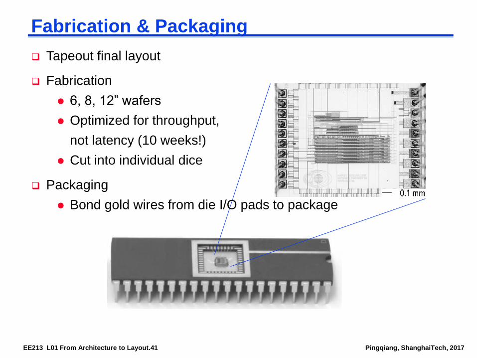
Fabrication & Packaging
Tapeout final layout
Fabrication
6, 8, 12” wafers
Optimized for throughput,
not latency (10 weeks!)
Cut into individual dice
Packaging
Bond gold wires from die I/O pads to package

EE213 L01 From Architecture to Layout.42 Pingqiang, ShanghaiTech, 2017
Testing
Test that chip operates
Design errors
Manufacturing errors
A single dust particle or wafer defect kills a die
Yields from 90% to < 10%
Depends on die size, maturity of process
Test each part before shipping to customer

EE213 L01 From Architecture to Layout.43 Pingqiang, ShanghaiTech, 2017
MIPS R3000 Processor
32-bit 2nd generation commercial processor (1988)
Led by John Hennessy (Stanford, MIPS Founder)
32-64 KB Caches
1.2 mm process
111K Transistors
Up to 12-40 MHz
66 mm2 die
145 I/O Pins
VDD = 5 V
4 Watts

EE213 L01 From Architecture to Layout.44 Pingqiang, ShanghaiTech, 2017
Readings (check course page)
“ASIC-design-flow-prime” from IBM.


![1.[8%] Find the Thevenin equivalent to the left of the ...sist.shanghaitech.edu.cn/.../Teaching/Fall17/Assignments/hw8_sol.pdf · Electric Circuits, Fall 2017 HW8 Solution 1 / 19](https://img.pdfslide.net/doc/110x75/5af4db1d7f8b9a92718e1cfd/18-find-the-thevenin-equivalent-to-the-left-of-the-sist-circuits-fall-2017.jpg)